JP3631551B2 - Optical encoder - Google Patents
Optical encoder Download PDFInfo
- Publication number
- JP3631551B2 JP3631551B2 JP02859696A JP2859696A JP3631551B2 JP 3631551 B2 JP3631551 B2 JP 3631551B2 JP 02859696 A JP02859696 A JP 02859696A JP 2859696 A JP2859696 A JP 2859696A JP 3631551 B2 JP3631551 B2 JP 3631551B2
- Authority
- JP
- Japan
- Prior art keywords
- light receiving
- light
- light source
- scale
- element array
- Prior art date
- Legal status (The legal status is an assumption and is not a legal conclusion. Google has not performed a legal analysis and makes no representation as to the accuracy of the status listed.)
- Expired - Fee Related
Links
- 230000003287 optical effect Effects 0.000 title claims description 38
- 239000000758 substrate Substances 0.000 claims description 57
- 238000006073 displacement reaction Methods 0.000 claims description 48
- 230000005540 biological transmission Effects 0.000 claims description 21
- 230000001678 irradiating effect Effects 0.000 claims description 16
- 239000004065 semiconductor Substances 0.000 claims description 13
- 230000000737 periodic effect Effects 0.000 claims description 4
- 239000011295 pitch Substances 0.000 description 36
- 238000000034 method Methods 0.000 description 18
- 230000000694 effects Effects 0.000 description 7
- XUIMIQQOPSSXEZ-UHFFFAOYSA-N Silicon Chemical compound [Si] XUIMIQQOPSSXEZ-UHFFFAOYSA-N 0.000 description 6
- 229910052710 silicon Inorganic materials 0.000 description 6
- 239000010703 silicon Substances 0.000 description 6
- 238000009826 distribution Methods 0.000 description 4
- 238000005304 joining Methods 0.000 description 3
- 238000005286 illumination Methods 0.000 description 2
- 239000002184 metal Substances 0.000 description 2
- 238000000059 patterning Methods 0.000 description 2
- 238000007740 vapor deposition Methods 0.000 description 2
- 240000007124 Brassica oleracea Species 0.000 description 1
- 235000003899 Brassica oleracea var acephala Nutrition 0.000 description 1
- 235000012905 Brassica oleracea var viridis Nutrition 0.000 description 1
- 230000002411 adverse Effects 0.000 description 1
- 229910021417 amorphous silicon Inorganic materials 0.000 description 1
- 238000003491 array Methods 0.000 description 1
- 238000009792 diffusion process Methods 0.000 description 1
- 238000005516 engineering process Methods 0.000 description 1
- 230000010354 integration Effects 0.000 description 1
- 238000004519 manufacturing process Methods 0.000 description 1
- 230000007261 regionalization Effects 0.000 description 1
Images


Classifications
-
- H—ELECTRICITY
- H03—ELECTRONIC CIRCUITRY
- H03M—CODING; DECODING; CODE CONVERSION IN GENERAL
- H03M1/00—Analogue/digital conversion; Digital/analogue conversion
- H03M1/12—Analogue/digital converters
- H03M1/22—Analogue/digital converters pattern-reading type
- H03M1/24—Analogue/digital converters pattern-reading type using relatively movable reader and disc or strip
- H03M1/28—Analogue/digital converters pattern-reading type using relatively movable reader and disc or strip with non-weighted coding
- H03M1/30—Analogue/digital converters pattern-reading type using relatively movable reader and disc or strip with non-weighted coding incremental
- H03M1/301—Constructional details of parts relevant to the encoding mechanism, e.g. pattern carriers, pattern sensors
-
- G—PHYSICS
- G01—MEASURING; TESTING
- G01D—MEASURING NOT SPECIALLY ADAPTED FOR A SPECIFIC VARIABLE; ARRANGEMENTS FOR MEASURING TWO OR MORE VARIABLES NOT COVERED IN A SINGLE OTHER SUBCLASS; TARIFF METERING APPARATUS; MEASURING OR TESTING NOT OTHERWISE PROVIDED FOR
- G01D5/00—Mechanical means for transferring the output of a sensing member; Means for converting the output of a sensing member to another variable where the form or nature of the sensing member does not constrain the means for converting; Transducers not specially adapted for a specific variable
- G01D5/26—Mechanical means for transferring the output of a sensing member; Means for converting the output of a sensing member to another variable where the form or nature of the sensing member does not constrain the means for converting; Transducers not specially adapted for a specific variable characterised by optical transfer means, i.e. using infrared, visible, or ultraviolet light
- G01D5/32—Mechanical means for transferring the output of a sensing member; Means for converting the output of a sensing member to another variable where the form or nature of the sensing member does not constrain the means for converting; Transducers not specially adapted for a specific variable characterised by optical transfer means, i.e. using infrared, visible, or ultraviolet light with attenuation or whole or partial obturation of beams of light
- G01D5/34—Mechanical means for transferring the output of a sensing member; Means for converting the output of a sensing member to another variable where the form or nature of the sensing member does not constrain the means for converting; Transducers not specially adapted for a specific variable characterised by optical transfer means, i.e. using infrared, visible, or ultraviolet light with attenuation or whole or partial obturation of beams of light the beams of light being detected by photocells
- G01D5/36—Forming the light into pulses
- G01D5/38—Forming the light into pulses by diffraction gratings
Landscapes
- Physics & Mathematics (AREA)
- General Physics & Mathematics (AREA)
- Engineering & Computer Science (AREA)
- Theoretical Computer Science (AREA)
- Optical Transform (AREA)
- Length Measuring Devices By Optical Means (AREA)
Description
【0001】
【発明の属する技術分野】
この発明は、所定ギャップをおいて相対移動可能に配置された第1,第2の部材の相対変位を光学的に測定する光学式エンコーダに関する。
【0002】
【従来の技術】
二つの部材間の相対変位を光学的に測定する光学式エンコーダは、基本的に2種の格子の重なりの変化による明暗パターンの変化を検出するもので、それぞれ所定ピッチの格子が形成されたメインスケールとインデックススケールを用いて構成される。メインスケールによる明暗像を得るための照射光としてコリメート光を用いると、スケールピッチを微細化したときに回折の影響が大きくなり、明瞭なメインスケールによる明暗像が得られにくくなる。
【0003】
これに対して、積極的に回折像パターンを利用する方式の光学式エンコーダもある。例えば、光源波長に近いピッチのメインスケールを用い、コリメート光をメインスケールに照射して、±1次回折光と0次光(非回折光)が重なるギャップ位置でピーク値を示すスケールパターンに対応する明暗像パターンを得ることができる。但しこの方式は、所定のギャップ位置から外れると明瞭な明暗パターンが得らず、メインスケールの格子ピッチをP、光源波長をλとして、メインスケールから距離P2/λ(またはその整数倍)の位置に正確にインデックススケールを配置することが必要になる。例えば、スケール格子ピッチP=8μm 、光源波長λ=700nmとすると、P2/λ=91.4μm となる。この様な小さいギャップを正確に調整することは難しく、また位置決めができたとしても僅かなギャップ変動がS/Nを大きく劣化させる。
【0004】
この様な難点を解消する方式として、拡散光源を用い、インデックススケールを光源側と受光側に配置して、3個の格子の重なりの変化を利用するようにしたいわゆる3格子システムが知られている。即ち図18に示すように、メインスケール1に対して受光側インデックススケール3と光源側インデックススケール2の3格子を用いる。光源4としてはLED等の拡散光源を用い、インデックススケール2により所定ピッチP2の二次光源アレイを得る。この二次光源アレイからの照明によるメインスケール1の明暗パターンを受光側インデックススケール3で変調することにより、受光素子5でスケール変位に対応して変化する出力信号を得る。
【0005】
この様な3格子システムを、図19に示すような反射型として構成して、光源側インデックススケール2と受光側インデックススケール3を共有させる方式は、例えば特公昭60−23282号公報に示されている。この公報において、メインスケールとインデックススケールの格子ピッチの関係を設定することより、幾何光学像パターンを検出する方式(以下、幾何光学方式)とすることができ、また回折像パターンを得る方式(以下、回折効果方式)とすることもできることが示されている。
【0006】
図20(a)(b)はそれぞれ幾何光学方式と回折効果方式のスケール格子と像パターンの例を示している。反射型の場合、各ケール間距離は、u=vである。図20(a)の幾何光学方式の場合、メインスケールピッチP1に対して、光源側及び受光側のインデックススケールピッチをP2=P3=2P1として、メインスケールを直進する光成分の重ね合わせによる明暗パターンが得られる。図20(b)の回折効果方式の場合は、P2=P3=P1として、メインスケールでの±1次回折光と0次光の重なりによる明暗パターンを得ることができる。
【0007】
特公昭60−23282号公報の技術は、図20の例に示すように、P2=P3として、光源側インデックススケールと受光側インデックススケールを共用させるものであるが、これに対して、同様の3格子システムの反射型の光学エンコーダであって、光源用インデックススケールと受光用インデックススケールを共通基板を用いて別々の格子ピッチで形成することにより、格子ピッチの設計の自由度を増す技術が、例えば実公平7−888号公報に示されている。
【0008】
【発明が解決しようとする課題】
従来提案されている3格子システムの反射型の光学式エンコーダにおいては、受光側のインデックススケールで90°位相のずれた二つの変位出力信号を得るためには、空間的位相を異ならせた二つの格子部を別々の部位に設けることが必要であり、更にこれらと位相が180°ずれた変位出力信号を得るためには、更に二つの格子部を別の部位に設けることが必要になる。このため、変位出力信号が光量分布やスケールのムラの影響を受け易い。従って、スケール部材のアラインメント調整が難しく、ヨウ、ピッチ、ロール等の僅かな機械的回転が特性を大きく劣化させるという問題がある。
【0009】
一方、受光側インデックススケールを兼ねて受光素子アレイを用いる方式が考えられるが、この場合光源側インデックススケールと受光素子アレイの取り付けの際のアラインメント調整が必要であり、僅かの調整ズレが特性を劣化させる。更にスケールピッチを微細化した場合、スケールピッチの微細化に対応させた受光素子アレイの微細化が製造技術上難しいという問題がある。
【0010】
この発明は、上記事情を考慮してなされたもので、難しいギャップ調整やアラインメント調整を要せず、高分解能特性を得ることを可能とした光学式エンコーダを提供することを目的としている。
【0011】
【課題を解決するための手段】
この発明は、所定ギャップをおいて相対移動可能に配置された第1,第2の部材の相対変位を光学的に測定するエンコーダにおいて、前記第1の部材は、反射部と非反射部が所定ピッチで配列されて反射型格子を構成するメインスケールを有し、前記第2の部材は、前記メインスケールを照射して所定の反射像パターンを生じさせる光照射手段と、前記メインスケールから得られる反射像パターンを検出する受光手段とを有し、前記光照射手段は、拡散光を出す光源と、光透過部と不透過部が所定ピッチで配列されて透過型格子を構成して前記メインスケールを照射する二次光源アレイとなる光源用インデックススケールとから構成され、前記受光手段は、半導体基板に複数の受光素子が配列形成されて前記反射像パターンを前記相対変位に応じて変調した変位出力信号を得ると共に隣接する前記受光素子間で異なる位相の前記変位出力信号を得る受光素子アレイにより構成され、且つ、前記受光素子アレイと前記光源用インデックススケールは、前記受光素子アレイの受光面と前記光源用インデックススケールの透過型格子面を揃えて一体に構成されており、前記受光素子アレイと前記光源用インデックススケールは、前記受光素子アレイの受光面と前記光源用インデックススケールの透過型格子面とが前記メインスケールに対向する側で同一面となるように一体に接合されており、前記光源用インデックススケールは、透明基板を用いてこの透明基板の前記光源側の面と反対側の面に前記透過型格子が形成されたものであることを特徴とする。
この発明は、また、所定ギャップをおいて相対移動可能に配置された第1,第2の部材の相対変位を光学的に測定するエンコーダにおいて、前記第1の部材は、反射部と非反射部が所定ピッチで配列されて反射型格子を構成するメインスケールを有し、前記第2の部材は、前記メインスケールを照射して所定の反射像パターンを生じさせる光照射手段と、前記メインスケールから得られる反射像パターンを検出する受光手段とを有し、前記光照射手段は、拡散光を出す光源と、光透過部と不透過部が所定ピッチで配列されて透過型格子を構成して前記メインスケールを照射する二次光源アレイとなる光源用インデックススケールとから構成され、前記受光手段は、半導体基板に複数の受光素子が配列形成されて前記反射像パターンを前記相対変位に応じて変調した変位出力信号を得ると共に隣接する前記受光素子間で異なる位相の前記変位出力信号を得る受光素子アレイにより構成され、且つ、前記受光素子アレイと前記光源用インデックススケールは、前記受光素子アレイの受光面と前記光源用インデックススケールの透過型格子面を揃えて一体に構成されており、前記光源用インデックススケールは、透明基板を用いてこの透明基板の前記光源側の面に透過型格子が形成されたものであり、前記受光素子アレイは、前記透明基板の前記透過型格子が形成された領域に隣接する位置に前記受光面を前記透過型格子が形成された面と対向させて搭載されており、前記光源用インデックススケールと前記受光素子アレイとは、前記透明基板を共通基板として一体化されており、前記透過型格子、前記透明基板、前記メインスケールの順番で配置されていることを特徴とする。
【0012】
この発明は、また、所定ギャップをおいて相対移動可能に配置された第1,第2の部材の相対変位を光学的に測定するエンコーダにおいて、前記第1の部材は、反射部と非反射部が所定ピッチで配列されて反射型格子を構成するメインスケールを有し、前記第2の部材は、前記メインスケールを照射して所定の反射像パターンを生じさせる光照射手段と、前記メインスケールから得られる反射像パターンを検出する受光手段とを有し、前記光照射手段は、拡散光を出す光源と、光透過部と不透過部が所定ピッチで配列されて透過型格子を構成して前記メインスケールを照射する二次光源アレイとなる光源用インデックススケールとから構成され、前記受光手段は、半導体基板に複数の受光素子が配列形成されて前記反射像パターンを前記相対変位に応じて変調した変位出力信号を得ると共に隣接する前記受光素子間で異なる位相の前記変位出力信号を得る受光素子アレイにより構成され、且つ、前記受光素子アレイと前記光源用インデックススケールは、前記受光素子アレイの受光面と前記光源用インデックススケールの透過型格子面を揃えて一体に構成されており、前記受光素子アレイは、前記光源用インデックススケールの前記相対変位方向の中央部に搭載され、前記光源用インデックススケールは前記受光素子アレイが搭載された領域の周囲に前記透過型格子が形成されていることを特徴とする。
この発明はまた、複数個の光源用インデックススケールを備えて、これら複数個の光源用インデックススケールが、前記受光素子アレイの周囲に配置されて前記受光素子アレイの受光面と前記複数の光源用インデックススケールの透過型格子面とを揃えて前記受光素子アレイと一体に構成されていることを特徴としている。
【0013】
更にこの発明において好ましくは、前記受光素子アレイの前面に、前記メインスケールの格子とは所定角度傾斜した光透過部と不透過部が配列形成されてメインスケールとの間でモアレ縞を生じさせる透過型格子を構成する受光用インデックススケールが更に配置され、前記受光素子アレイは、半導体基板に前記モアレ縞を検出するための複数の受光素子が前記モアレ縞の周期方向に配列形成されたものとする。
更にまたこの発明において好ましくは、前記メインスケールの格子と前記光源用インデックススケールの格子とは、モアレ縞を生じさせるべく互いに所定角度傾斜させて配列され、前記受光素子アレイは、半導体基板に前記モアレ縞を検出するための複数の受光素子が前記モアレ縞の周期方向に配列形成されたものとする。
【0014】
この発明に係る光学式エンコーダは、3格子システムの反射型エンコーダであって、受光側のインデックススケールを兼ねた受光素子アレイが光源用インデックススケールと一体に構成されているため、これらの取り付けの際のアラインメント調整が要らず、高性能特性を得ることができる。また、受光用インデックススケールを用いた場合と異なり、狭い受光面範囲で2相あるいは4相の変位出力信号を得ることができる。従って、スケール取付のアラインメント誤差の影響が小さく、4相間のバランスがよい出力信号を得ることができ、電気的調整が不要となる。
またこの発明において、モアレ縞を生じさせる受光用インデックススケールを配置し、あるいは光源用インデックススケールとメインスケールの間でモアレ縞を生じさせて、モアレ縞を検出する方式とすることにより、受光素子アレイの配列ピッチをそれ程微細化する事なく、高分解能特性を得ることができる。
【0015】
【発明の実施の形態】
以下、図面を参照して、この発明の実施例を説明する。
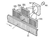
図1は、この発明の一実施例に係る光学式エンコーダの構成を示す斜視図であり、図2はその主要部の平面図である。第1の部材10と第2の部材20が所定ギャップをもって、矢印xで示すように相対移動可能に配置される。第1の部材10の第2の部材20に対向する面にはメインスケールG1が取り付けられている。メインスケールG1は、基板31にAl膜等による光反射部32と非反射部33(光透過部または光吸収部)とが所定ピッチPsで配列形成された反射型のスケールである。
【0016】
第2の部材20の第1の部材10に対向する面には、メインスケールG1を照射する手段として、拡散光源であるLED40とその拡散光を受けて二次光源アレイを構成する光源用インデックススケールG2、及びメインスケールG1からの反射像パターンを受光するフォトダイオードアレイPDAが配置されている。光源用インデックススケールG2は、透明基板51のメインスケールG1に対向する側の面にCr膜等による不透過部52と光透過部53とを所定ピッチPaで配列形成した透過型格子である。フォトダイオードアレイPDAは、例えばn型シリコン基板61にp型層を拡散形成したフォトダイオード62を所定ピッチPbで配列形成したものである。
【0017】
この実施例においては、フォトダイオードアレイPDAのシリコン基板61と光源用インデックススケールG2の透明基板51とは、同じ厚みを有し、それらの側面が接合されて一体化された状態で第2の部材20に取り付けられている。
【0018】
メインスケールG1のピッチPsと光源用インデックススケールG2のピッチPaとは、フォトダイオードアレイPDAの面上の幾何光学像パターンを検出する場合には、Pa=2n・Ps(nは正の整数)を満たすように設定される。また、回折像パターンを検出する場合には、Pa=n・Psを満たすように設定される。
メインスケールG1のピッチPsとフォトダイオードアレイPDAのピッチPbとの関係は例えば、図3に具体例を示したように、各フォトダイオード62の幅がPs/2、間隔がPs/4、従って、Pb=3Ps/4を満たすように設定される。これによりフォトダイオードアレイPDAからは、スケール変位xに応じて図4に示すように、A,B,AB,BBの4相の出力電流が得られる。
【0019】
これらの4相出力電流は、それぞれ電流電圧変換器63a〜63dにより電圧値に変換された後、差動増幅器64a,64bにより互いに180°位相がずれたA,AB相間、及びB,BB相間の差動がとられて、互いに90°位相がずれたA,B相の二つの変位信号が得られる。これらの変位信号を公知の方法で処理することにより、スケール変位が求められる。
【0020】
この実施例によると、受光部にはインデックススケールを用いることなく、実質的に3格子システムを応用した反射型の光学式エンコーダが得られる。また、フォトダイオードアレイPDAと光源用インデックススケールG2とは基板を同じ厚みとしてこれらを接合して一体化しているため、これらを別々に取り付けた場合に生じる相対的な傾き等のアラインメント誤差が生じない。
【0021】
また、受光用インデックススケールを用いる方式では、2相の変位出力信号のために空間的に離れた位置に二つの格子部を必要とし、4相の変位出力信号を得るためには空間的に離れた4個の格子部を必要とするのに対し、隣接フォトダイオードが異なる位相の変位出力を出すようにフォトダイオードを配列したフォトダイオードアレイPDAを用いるこの実施例の方式では狭い受光面範囲で4相の変位出力信号を得ることができる。従って、光量分布のアンバランスの影響やスケール取付のアラインメント誤差の影響が小さい。
【0022】
また、実公平7−888号公報に示されているように、光源用と受光用のインデックススケールを共通基板に形成すると、光源と受光素子はこのインデックススケールの同じ側に配置されるため、インデックススケールで直接反射されて受光素子に入る拡散光成分が無視できず、これが出力信号に重畳されて悪影響を与える。この実施例によると、光源用インデックススケールG2からの拡散光成分がメインスケールG1に入らずに直接フォトダイオードアレイPDAに漏れ込むということがなく、出力信号のS/Nが高いものとなる。
【0023】
図5は、別の実施例の光学式エンコーダの要部構成を図2に対応させて示す。先の実施例と異なる点を説明すれば、この実施例では、光源用インデックススケールG2は、透明基板51の光源40側の面に光透過部53と不透過部52を配列してスケール格子を形成している。そして同じ透明基板51のスケール格子部に隣接する位置に、フォトダイオードアレイPDAが受光面を下にして搭載されている。つまり、透明基板51を共通基板として用いて光源用インデックススケールG2とフォトダイオードアレイPDAが一体化されている。
この実施例によると、光源用インデックススケールG2とフォトダイオードアレイPDAの一体化が、側面を接合する先の実施例より容易になる。
【0024】
図6は、更に別の実施例の光学式エンコーダである。この実施例は図1の実施例を基本として、フォトダイオードアレイPDAの両サイドに光源用インデックススケールG2a,G2bを配置し、更にフォトダイオードアレイPDAの上部にも光源用インデックススケールG2cを配置して、光源40からの拡散光をレンズ70により更に拡大してこれらのインデックススケールG2a〜G2cに照射するようにしたものである。この場合も、インデックススケールG2a〜G2cとフォトダイオードアレイPDAは、基板厚みを揃えて側面を接合して一体化される。
この実施例によると、フォトダイオードアレイPDAの受光面に3方からの照明によるメインスケールG1の反射像パターンが投影されるから、フォトダイオードアレイPDA上の光量分布が均一になる。
【0025】
図7は、図5の構成法を利用して、実質的に図6と同様の構成を実現した実施例である。フォトダイオードアレイPDAは、光源用インデックススケールG2の透明基板51の透過型格子が形成された光源側の面の相対変位方向の中央部に受光面を下向きにして搭載されている。光源用インデックススケールG2の透過型格子は、フォトダイオードアレイPDAの周囲に、即ちフォトダイオードアレイPDAを挟む左右領域およびフォトダイオードアレイPDAの上部に形成されている。
この実施例によると、1枚の光源用インデックススケール基板を用いて、実質的に図6と同様の構成が得られるから、アラインメントが容易である。
【0026】
図8は、モアレ縞パターンを得る方式の光学式エンコーダの実施例の要部構成を示す斜視図であり、図9はその平面図である。メインスケールG1と光源用インデックススケールG2及び拡散光源40の部分は、図5の実施例と同様である。光源用インデックススケールG2を形成した透明基板51上にこの実施では、メインスケール格子に対して僅かに傾斜した光透過部82と不透過部81の配列によるモアレ縞生成用の受光用インデックススケールG3が形成されている。この受光用インデックススケールG3の不透過部81と光透過部82は、光源用インデックススケールG2の不透過部52と透過部52と同時に透明基板51上にパターン形成される。
【0027】
フォトダイオードアレイPDAは、受光用インデックススケールG3の格子面にその受光面を下にして搭載されている。フォトダイオードアレイPDAは、n型シリコン基板91にp型層によるフォトダイオード92を形成したものであるが、フォトダイオード92の配列方向は先の実施例と異なり、形成されるモアレ縞の周期方向に配列される。
【0028】
図10は、メインスケールG1と受光用インデックススケールG3により形成されるモアレ縞とフォトダイオードアレイPDAの関係を示す。図示のように各格子のピッチdと格子の傾斜角θにより決まるモアレ縞が得られ、そのモアレ縞の1周期Pmに対して、3Pm/4のピッチでフォトダイオード92を配列することにより、スケール変位に伴うモアレ縞の変位によって、A,BB,AB,Bの4相の変位信号を得ることができる。
【0029】
この実施例によると、スケールピッチを微細化した場合にも、モアレにより実質的にスケールピッチを拡大することができ、フォトダイオードアレイPDAの製造が容易になる。具体的に、例えばメインスケールG1の格子ピッチPs、光源用インデックススケールG2の格子ピッチPa、受光用インデックススケールG3の格子ピッチPbを、Ps=Pa=Pb=8μm (=d)とし、θ≒23.074°として、フォトダイオードアレイPDAは、ダイオード幅10μm 、ピッチ15μm で配列することができる。
【0030】
図11及び図12は、上記実施例を変形した実施例のそれぞれ図8及び図9に対応する構成である。この実施例では、モアレ用の受光用インデックススケールG3は光源用インデックススケールG2とは別に、フォトダイオードアレイPDAの受光面上に、金属膜の蒸着とパターニングによって不透過部81と光透過部82を形成して作られる。図13はその様子を拡大して示した斜視図である。フォトダイオードアレイPDAの受光面は例えばSiO2のような絶縁膜93で覆われ、この上に受光用インデックススケールパターンが形成される。
【0031】
そして、光源用インデックススケールG2の透明基板51とフォトダイオードアレイPDAのシリコン基板91を、図1の実施例と同様に同じ厚みとしてそれらの側面を接合して一体化している。
なおこの実施例のように受光用インデックススケールG3を一体形成したフォトダイオードアレイPDAを、図8の実施例と同様に光源用インデックススケールG2の基板上に搭載して光源用インデックススケールG2と一体化することもできる。
【0032】
図14及び図15は、モアレ方式の反射型エンコーダの他の実施例を示す要部斜視図と平面図である。この実施例では、モアレ用の透過型インデックススケールG23を光源側に配置して、これを二次光源アレイを得るための透過型格子としても用いるようにしたものである。このフォトダイオードアレイPDAの基板とインデックススケールG23の基板は同じ厚みを有し、図1の実施例と同様に側面を接合して一体化されている。言い換えれば、図11におけるモアレ用インデックススケールG3と光源側インデックススケールG2を共有として光源側に配置したものである。この方式は、光源用インデックススケールG23とメインスケールG1との格子間でモアレ縞を生じさせるもので、フォトダイオードアレイPDAの受光面積を大きく確保できる点で有利である。
【0033】
図16及び図17は、更に別の実施例のモアレ方式の反射型エンコーダを示す要部斜視図と平面図である。モアレ用を兼ねた光源側のインデックススケールG23が、透明基板51の光源側の面に光透過部53と不透過部52を配列形成して構成されている。そして同じ透明基板51の格子部に隣接する位置にフォトダイオードアレイPDAがその受光面を下にして搭載されている。
この実施例によっても先の実施例と同様の効果が得られる。
【0034】
なお図14〜図17の実施例は、光源側インデックススケールの格子をメインスケールの格子に対して傾斜させたが、この傾斜は相対的なものであるから、光源側インデックススケールは通常通りスケール変位方向に対しては直交する方向とし、メインスケールの格子をスケール変位方向に直交する方向から僅かに傾斜させたパターンとすることによっても、同様のモアレ縞を得ることができる。
【0035】
この発明は上記実施例に限られない。例えば上記実施例では、光源用インデックススケールとフォトダイオードアレイはそれぞれ別個に形成した後に接合して一体化したが、インデックススケール基板上にアモルファスシリコン等の半導体膜を堆積して、この半導体膜を利用してフォトダイオードアレイを配列形成することもできる。フォトダイオードに代わってフォトトランジスタを用いることもできる。
また、光源用インデックススケールと拡散光源としてのLEDを一体的に形成することも可能である。例えば、大きな発光面を持つLEDの発光面上に直接インデックススケール格子を金属膜の蒸着、パターニングによって形成することができる。
【0036】
【発明の効果】
以上述べたようにこの発明によれば、3格子システムの反射型エンコーダであって、受光側のインデックススケールを兼ねた受光素子アレイを光源用インデックススケールと一体に構成することにより、受光素子アレイと光源用インデックススケールとの間のアラインメント調整が要らず、高性能特性を得ることができる。また、受光用インデックススケールを用いた場合と異なり、狭い受光面範囲で2相あるいは4相の変位出力信号を得ることができ、光量分布のばらつきやアラインメント誤差の影響が小さく、4相間のバランスがよい出力信号を得ることができて電気的調整が不要となる。
またこの発明によると、モアレ縞を生じさせる受光用インデックススケールを配置し、あるいは光源用インデックススケールとメインスケールの間でモアレ縞を生じさせて、モアレ縞を検出する方式とすることにより、受光素子アレイの配列ピッチをそれ程微細化する事なく、高分解能特性を得ることができる。
【図面の簡単な説明】
【図1】この発明の一実施例に係る光学式エンコーダの構成を示す斜視図である。
【図2】同実施例の要部構成を示す平面図である。
【図3】同実施例のメインスケールとフォトダイオードアレイの配列関係を示す。
【図4】同実施例の出力電流特性を示す。
【図5】他の実施例の光学式エンコーダの要部構成を示す平面図である。
【図6】他の実施例の光学式エンコーダの要部構成を示す斜視図である。
【図7】他の実施例の光学式エンコーダの要部構成を示す斜視図である。
【図8】他の実施例の光学式エンコーダの要部構成を示す斜視図である。
【図9】同実施例の光学式エンコーダの要部構成を示す平面図である。
【図10】同実施例のモアレ縞とフォトダイオードアレイの関係を示す。
【図11】他の実施例の光学式エンコーダの要部構成を示す斜視図である。
【図12】同実施例の光学式エンコーダの要部構成を示す平面図である。
【図13】同実施例のフォトダイオードアレイの構成を示す斜視図である。
【図14】他の実施例の光学式エンコーダの要部構成を示す斜視図である。
【図15】同実施例の光学式エンコーダの要部構成を示す平面図である。
【図16】他の実施例の光学式エンコーダの要部構成を示す斜視図である。
【図17】同実施例の光学式エンコーダの要部構成を示す平面図である。
【図18】3格子システムの透過型光学式エンコーダの構成を示す。
【図19】3格子システムの反射型光学式エンコーダの構成を示す。
【図20】3格子システムの明暗像パターン形成原理を示す。
【符号の説明】
10…第1の部材、20…第2の部材、G1…メインスケール、31…基板、32…光反射部、33…非反射部、G2…光源用インデックススケール、51…透明基板、52…不透過部、53…光透過部、40…拡散光源、PDA…フォトダイオードアレイ、61…シリコン基板、62…フォトダイオード、G3…受光用インデックススケール(モアレ用)、81…不透過部、82…光透過部、91…シリコン基板、92…フォトダイオード。[0001]
BACKGROUND OF THE INVENTION
The present invention relates to an optical encoder that optically measures the relative displacement of first and second members arranged to be relatively movable with a predetermined gap.
[0002]
[Prior art]
An optical encoder that optically measures the relative displacement between two members basically detects changes in the light-dark pattern due to changes in the overlap of two types of gratings. Consists of a scale and an index scale. When collimated light is used as irradiation light for obtaining a bright and dark image on the main scale, the influence of diffraction increases when the scale pitch is reduced, and it becomes difficult to obtain a clear and dark image on the main scale.
[0003]
On the other hand, there is an optical encoder of a type that positively uses a diffraction pattern. For example, a main scale having a pitch close to the light source wavelength is used, collimated light is applied to the main scale, and a scale pattern that shows a peak value at a gap position where ± first-order diffracted light and zero-order light (non-diffracted light) overlap is supported. A bright and dark image pattern can be obtained. However, in this method, a clear light / dark pattern cannot be obtained when it is out of a predetermined gap position, the distance P from the main scale is P, where P is the grating pitch of the main scale, and λ is the light source wavelength.2It is necessary to accurately place the index scale at the position of / λ (or an integer multiple thereof). For example, when the scale grating pitch P = 8 μm and the light source wavelength λ = 700 nm, P2/Λ=91.4 μm. It is difficult to accurately adjust such a small gap, and even if positioning can be performed, slight gap fluctuation greatly deteriorates the S / N.
[0004]
As a method for solving such difficulties, a so-called three-grid system is known in which a diffused light source is used and index scales are arranged on the light source side and the light-receiving side so as to use a change in the overlap of three lattices. Yes. That is, as shown in FIG. 18, three grids of the light receiving
[0005]
A system in which such a three-grating system is configured as a reflection type as shown in FIG. 19 and the light source
[0006]
FIGS. 20A and 20B show examples of the scale grating and the image pattern of the geometric optical method and the diffraction effect method, respectively. In the reflection type, the distance between each kale is u = v. In the case of the geometric optical system of FIG. 20A, the light and dark pattern by superimposing the light components traveling straight through the main scale, with the index scale pitch of the light source side and the light receiving side set to P2 = P3 = 2P1 with respect to the main scale pitch P1. Is obtained. In the case of the diffraction effect method of FIG. 20B, P2 = P3 = P1, and a light / dark pattern due to the overlap of ± 1st order diffracted light and 0th order light on the main scale can be obtained.
[0007]
In the technique of Japanese Patent Publication No. 60-23282, as shown in the example of FIG. 20, P2 = P3 and the light source side index scale and the light receiving side index scale are shared. A reflection type optical encoder for a grating system, in which a light source index scale and a light receiving index scale are formed at different grating pitches using a common substrate, thereby increasing the degree of freedom in designing the grating pitch. This is shown in Japanese Utility Model Publication No. 7-888.
[0008]
[Problems to be solved by the invention]
In the conventional reflection type optical encoder of the three-grating system, in order to obtain two displacement output signals that are 90 ° out of phase on the index scale on the light receiving side, two spatially phased two different output signals are obtained. It is necessary to provide the grating portions in different parts, and in order to obtain a displacement output signal whose phase is shifted by 180 ° from these, it is necessary to further provide two grating parts in different parts. For this reason, the displacement output signal is easily affected by the light amount distribution and the unevenness of the scale. Therefore, it is difficult to adjust the alignment of the scale member, and there is a problem that slight mechanical rotation of the yaw, pitch, roll, etc. greatly deteriorates the characteristics.
[0009]
On the other hand, a method of using a light receiving element array that also serves as a light receiving side index scale is conceivable. In this case, alignment adjustment is required when attaching the light source side index scale and the light receiving element array, and a slight adjustment deviation deteriorates the characteristics. Let Further, when the scale pitch is miniaturized, there is a problem that the miniaturization of the light receiving element array corresponding to the miniaturization of the scale pitch is difficult in terms of manufacturing technology.
[0010]
The present invention has been made in consideration of the above circumstances, and an object thereof is to provide an optical encoder that can obtain high resolution characteristics without requiring difficult gap adjustment or alignment adjustment.
[0011]
[Means for Solving the Problems]
The present invention provides an encoder for optically measuring the relative displacement of first and second members arranged to be relatively movable with a predetermined gap, wherein the first member has a predetermined reflecting portion and a non-reflecting portion. The second member is obtained from the main scale, the light irradiating means for irradiating the main scale to generate a predetermined reflected image pattern, and having a main scale arranged at a pitch to constitute a reflective grating. A light receiving means for detecting a reflected image pattern, the light irradiating means comprising a light source that emits diffused light, a light transmitting portion and a non-transmitting portion arranged at a predetermined pitch to form a transmission type grating, and the main scale A light source index scale serving as a secondary light source array that irradiates the light source, and the light receiving means includes a plurality of light receiving elements arrayed on a semiconductor substrate to change the reflected image pattern to the relative displacement. And a light receiving element array that obtains a displacement output signal having a phase different between adjacent light receiving elements, and the light receiving element array and the light source index scale include the light receiving element. The light-receiving surface of the array and the transmission type grating surface of the index scale for light source are aligned and integrated, and the light-receiving element array and the index scale for light source are the light-receiving surface of the light-receiving element array and the index scale for light source. And the transmission type grating surface are integrally joined so as to be on the same surface on the side facing the main scale, and the light source index scale is made of a transparent substrate and the surface on the light source side of the transparent substrate. The transmission type grating is formed on the opposite surface.
The present invention also provides an encoder for optically measuring the relative displacement of the first and second members arranged so as to be relatively movable with a predetermined gap, wherein the first member includes a reflecting portion and a non-reflecting portion. Are arranged at a predetermined pitch to form a reflective grating, and the second member irradiates the main scale to generate a predetermined reflected image pattern; and A light receiving means for detecting the obtained reflected image pattern, the light irradiating means comprising a light source that emits diffused light, a light transmitting portion and a non-transmitting portion arranged at a predetermined pitch to form a transmissive grating, and A light source index scale serving as a secondary light source array for irradiating a main scale, and the light receiving means includes a plurality of light receiving elements arrayed on a semiconductor substrate, and the reflected image pattern is transferred to the relative scale. A light receiving element array that obtains a displacement output signal modulated according to the position and obtains the displacement output signal having a phase different between adjacent light receiving elements, and the light receiving element array and the light source index scale are The light receiving surface of the light receiving element array and the transmission type grating surface of the light source index scale are aligned and integrated, and the light source index scale is transmitted to the light source side surface of the transparent substrate using a transparent substrate. In the light receiving element array, the light receiving surface is opposed to the surface on which the transmissive grating is formed at a position adjacent to a region where the transmissive grating is formed on the transparent substrate. The light source index scale and the light receiving element array are integrated with the transparent substrate as a common substrate. Type grating, the transparent substrate, characterized in that it is arranged in the order of the main scale.
[0012]
The present invention also provides an encoder for optically measuring the relative displacement of the first and second members arranged so as to be relatively movable with a predetermined gap, wherein the first member includes a reflecting portion and a non-reflecting portion. Are arranged at a predetermined pitch to form a reflective grating, and the second member irradiates the main scale to generate a predetermined reflected image pattern; and A light receiving means for detecting the obtained reflected image pattern, the light irradiating means comprising a light source that emits diffused light, a light transmitting portion and a non-transmitting portion arranged at a predetermined pitch to form a transmissive grating, and A light source index scale serving as a secondary light source array for irradiating a main scale, and the light receiving means includes a plurality of light receiving elements arrayed on a semiconductor substrate, and the reflected image pattern is transferred to the relative scale. A light receiving element array that obtains a displacement output signal modulated according to the position and obtains the displacement output signal having a phase different between adjacent light receiving elements, and the light receiving element array and the light source index scale are The light receiving surface of the light receiving element array and the transmission type grating surface of the index scale for the light source are configured to be integrated, and the light receiving element array is mounted at the center of the relative displacement direction of the index scale for the light source, The light source index scale is characterized in that the transmission type grating is formed around a region where the light receiving element array is mounted.
The present invention also includes a plurality of light source index scales, and the plurality of light source index scales are arranged around the light receiving element array, and the light receiving surface of the light receiving element array and the plurality of light source indexes. It is characterized in that it is configured integrally with the light receiving element array with the scale transmissive lattice plane aligned.
[0013]
Further preferably, in the present invention, a light transmitting portion and a non-transmitting portion, which are inclined at a predetermined angle with respect to the grating of the main scale, are arranged on the front surface of the light receiving element array so as to generate moire fringes between the main scale. A light receiving index scale constituting a mold grating is further arranged, and the light receiving element array includes a plurality of light receiving elements for detecting the moire fringes arranged on a semiconductor substrate in a periodic direction of the moire fringes. .
Still preferably, in the present invention, the main scale grating and the light source index scale grating are arranged to be inclined at a predetermined angle to generate moire fringes, and the light receiving element array is arranged on a semiconductor substrate. It is assumed that a plurality of light receiving elements for detecting fringes are arranged in the periodic direction of the moire fringes.
[0014]
The optical encoder according to the present invention is a reflective encoder of a three-grating system, and the light receiving element array that also serves as the index scale on the light receiving side is configured integrally with the index scale for the light source. Therefore, high-performance characteristics can be obtained. Further, unlike the case of using the light receiving index scale, a two-phase or four-phase displacement output signal can be obtained in a narrow light receiving surface range. Therefore, the influence of the alignment error of the scale mounting is small, and an output signal having a good balance between the four phases can be obtained, and electrical adjustment is not required.
In the present invention, a light receiving element array is provided by arranging a light receiving index scale for generating moire fringes, or generating moire fringes between a light source index scale and a main scale to detect moire fringes. High resolution characteristics can be obtained without making the arrangement pitch of the electrodes so fine.
[0015]
DETAILED DESCRIPTION OF THE INVENTION
Embodiments of the present invention will be described below with reference to the drawings.
FIG. 1 is a perspective view showing a configuration of an optical encoder according to an embodiment of the present invention, and FIG. 2 is a plan view of a main part thereof. The
[0016]
On the surface of the
[0017]
In this embodiment, the
[0018]
The pitch Ps of the main scale G1 and the pitch Pa of the light source index scale G2 are Pa = 2n · Ps (n is a positive integer) when detecting a geometric optical image pattern on the surface of the photodiode array PDA. Set to meet. Further, when detecting a diffraction pattern, it is set so as to satisfy Pa = n · Ps.
The relationship between the pitch Ps of the main scale G1 and the pitch Pb of the photodiode array PDA is, for example, as shown in a specific example in FIG. 3, the width of each
[0019]
These four-phase output currents are converted into voltage values by the current-voltage converters 63a to 63d, respectively, and thereafter, between the A and AB phases and between the B and BB phases that are 180 ° out of phase with each other by the
[0020]
According to this embodiment, it is possible to obtain a reflective optical encoder that substantially applies a three-grating system without using an index scale in the light receiving portion. Further, since the photodiode array PDA and the light source index scale G2 are integrated by joining the substrates with the same thickness, there is no alignment error such as relative inclination that occurs when they are separately attached. .
[0021]
Further, in the method using the light receiving index scale, two grid portions are required at spatially separated positions for a two-phase displacement output signal, and spatially separated to obtain a four-phase displacement output signal. However, in the method of this embodiment using a photodiode array PDA in which photodiodes are arranged so that adjacent photodiodes output displacement outputs having different phases, four grating portions are required. A phase displacement output signal can be obtained. Therefore, the influence of the unbalance of the light quantity distribution and the influence of the alignment error of the scale mounting are small.
[0022]
Further, as shown in Japanese Utility Model Publication No. 7-888, when the light source and light receiving index scales are formed on the common substrate, the light source and the light receiving element are arranged on the same side of the index scale. The diffused light component that is directly reflected by the scale and enters the light receiving element cannot be ignored, and this is superimposed on the output signal and has an adverse effect. According to this embodiment, the diffused light component from the light source index scale G2 does not directly enter the photodiode array PDA without entering the main scale G1, and the S / N of the output signal is high.
[0023]
FIG. 5 shows the configuration of the main part of an optical encoder according to another embodiment, corresponding to FIG. Explaining the difference from the previous embodiment, in this embodiment, the light source index scale G2 is formed by arranging a
According to this embodiment, the integration of the light source index scale G2 and the photodiode array PDA is easier than in the previous embodiment in which the side surfaces are joined.
[0024]
FIG. 6 shows an optical encoder according to still another embodiment. In this embodiment, the light source index scales G2a and G2b are disposed on both sides of the photodiode array PDA, and the light source index scale G2c is disposed on the photodiode array PDA. The diffused light from the
According to this embodiment, since the reflected image pattern of the main scale G1 by illumination from three directions is projected on the light receiving surface of the photodiode array PDA, the light amount distribution on the photodiode array PDA becomes uniform.
[0025]
FIG. 7 shows an embodiment in which the configuration similar to that of FIG. 6 is realized by using the configuration method of FIG. The photodiode array PDA is mounted with the light receiving surface facing downward in the center of the light source side surface on which the transmission type grating of the
According to this embodiment, since the same configuration as that of FIG. 6 can be obtained by using one index scale substrate for light source, alignment is easy.
[0026]
FIG. 8 is a perspective view showing a configuration of a main part of an embodiment of an optical encoder of a method for obtaining a moire fringe pattern, and FIG. 9 is a plan view thereof. The main scale G1, the light source index scale G2, and the diffused
[0027]
The photodiode array PDA is mounted on the grating surface of the light receiving index scale G3 with the light receiving surface facing downward. The photodiode array PDA is obtained by forming a
[0028]
FIG. 10 shows the relationship between the moire fringes formed by the main scale G1 and the light receiving index scale G3 and the photodiode array PDA. As shown in the figure, moire fringes determined by the pitch d of each grating and the inclination angle θ of the grating are obtained, and by arranging
[0029]
According to this embodiment, even when the scale pitch is miniaturized, the scale pitch can be substantially enlarged by moire, and the photodiode array PDA can be easily manufactured. Specifically, for example, the grating pitch Ps of the main scale G1, the grating pitch Pa of the light source index scale G2, and the grating pitch Pb of the light receiving index scale G3 are Ps = Pa = Pb = 8 μm (= d), and θ≈23. 0.074 °, the photodiode array PDA can be arranged with a diode width of 10 μm and a pitch of 15 μm.
[0030]
FIGS. 11 and 12 show configurations corresponding to FIGS. 8 and 9, respectively, of a modified example of the above embodiment. In this embodiment, the light receiving index scale G3 for moire is provided with an
[0031]
The
The photodiode array PDA in which the light receiving index scale G3 is integrally formed as in this embodiment is mounted on the substrate of the light source index scale G2 and integrated with the light source index scale G2 as in the embodiment of FIG. You can also
[0032]
FIGS. 14 and 15 are a perspective view and a plan view of a main part showing another embodiment of a moire type reflective encoder. In this embodiment, a transmissive index scale G23 for moire is arranged on the light source side, and this is used as a transmissive grating for obtaining a secondary light source array. The substrate of the photodiode array PDA and the substrate of the index scale G23 have the same thickness, and are integrated by joining the side surfaces as in the embodiment of FIG. In other words, the moire index scale G3 and the light source side index scale G2 in FIG. 11 are shared and arranged on the light source side. This method is advantageous in that moire fringes are generated between the gratings of the light source index scale G23 and the main scale G1, and a large light receiving area of the photodiode array PDA can be secured.
[0033]
FIGS. 16 and 17 are a perspective view and a plan view of a main part showing a moire type reflective encoder of still another embodiment. The index scale G23 on the light source side that also serves as a moire is configured by arranging a
According to this embodiment, the same effect as the previous embodiment can be obtained.
[0034]
14 to 17, the light source side index scale lattice is inclined with respect to the main scale lattice. However, since this inclination is relative, the light source side index scale is scale displacement as usual. Similar moire fringes can also be obtained by making the pattern perpendicular to the direction and slightly tilting the main scale grating from the direction perpendicular to the scale displacement direction.
[0035]
The present invention is not limited to the above embodiment. For example, in the above embodiment, the light source index scale and the photodiode array are separately formed and then joined and integrated. However, a semiconductor film such as amorphous silicon is deposited on the index scale substrate, and this semiconductor film is used. Thus, an array of photodiodes can be formed. A phototransistor can be used in place of the photodiode.
It is also possible to integrally form the light source index scale and the LED as the diffusion light source. For example, an index scale grating can be formed directly on the light emitting surface of an LED having a large light emitting surface by vapor deposition and patterning of a metal film.
[0036]
【The invention's effect】
As described above, according to the present invention, the reflection type encoder of the three-grating system, in which the light receiving element array that also serves as the index scale on the light receiving side is configured integrally with the light source index scale, No alignment adjustment with the light source index scale is required, and high performance characteristics can be obtained. Unlike the case of using the index scale for light reception, 2-phase or 4-phase displacement output signals can be obtained in a narrow light-receiving surface range, and the effect of variations in light intensity distribution and alignment errors is small, and the balance between the four phases is A good output signal can be obtained and electrical adjustment becomes unnecessary.
Further, according to the present invention, the light receiving element is configured to detect the moire fringes by arranging the light receiving index scale for generating moire fringes or generating the moire fringes between the light source index scale and the main scale. High resolution characteristics can be obtained without reducing the array pitch so much.
[Brief description of the drawings]
FIG. 1 is a perspective view showing a configuration of an optical encoder according to an embodiment of the present invention.
FIG. 2 is a plan view showing the main configuration of the embodiment.
FIG. 3 shows an arrangement relationship between a main scale and a photodiode array in the same example.
FIG. 4 shows output current characteristics of the same example.
FIG. 5 is a plan view showing a main configuration of an optical encoder according to another embodiment.
FIG. 6 is a perspective view showing a main configuration of an optical encoder according to another embodiment.
FIG. 7 is a perspective view showing a main configuration of an optical encoder according to another embodiment.
FIG. 8 is a perspective view showing a main configuration of an optical encoder according to another embodiment.
FIG. 9 is a plan view showing the main configuration of the optical encoder of the embodiment.
FIG. 10 shows the relationship between moire fringes and photodiode arrays in the same example.
FIG. 11 is a perspective view showing a main configuration of an optical encoder according to another embodiment.
FIG. 12 is a plan view showing a main configuration of the optical encoder according to the embodiment.
FIG. 13 is a perspective view showing the configuration of the photodiode array of the same example.
FIG. 14 is a perspective view showing a main configuration of an optical encoder according to another embodiment.
FIG. 15 is a plan view showing the main configuration of the optical encoder of the embodiment.
FIG. 16 is a perspective view showing a main configuration of an optical encoder according to another embodiment.
FIG. 17 is a plan view showing the main configuration of the optical encoder according to the embodiment.
FIG. 18 shows a configuration of a transmission optical encoder of a three-grating system.
FIG. 19 shows a configuration of a reflective optical encoder of a three-grating system.
FIG. 20 shows the principle of light / dark image pattern formation in a three-grating system.
[Explanation of symbols]
DESCRIPTION OF
Claims (6)
前記第1の部材は、反射部と非反射部が所定ピッチで配列されて反射型格子を構成するメインスケールを有し、
前記第2の部材は、前記メインスケールを照射して所定の反射像パターンを生じさせる光照射手段と、前記メインスケールから得られる反射像パターンを検出する受光手段とを有し、
前記光照射手段は、拡散光を出す光源と、光透過部と不透過部が所定ピッチで配列されて透過型格子を構成して前記メインスケールを照射する二次光源アレイとなる光源用インデックススケールとから構成され、
前記受光手段は、半導体基板に複数の受光素子が配列形成されて前記反射像パターンを前記相対変位に応じて変調した変位出力信号を得ると共に隣接する前記受光素子間で異なる位相の前記変位出力信号を得る受光素子アレイにより構成され、且つ、
前記受光素子アレイと前記光源用インデックススケールは、前記受光素子アレイの受光面と前記光源用インデックススケールの透過型格子面を揃えて一体に構成されており、
前記受光素子アレイと前記光源用インデックススケールは、前記受光素子アレイの受光面と前記光源用インデックススケールの透過型格子面とが前記メインスケールに対向する側で同一面となるように一体に接合されており、
前記光源用インデックススケールは、透明基板を用いてこの透明基板の前記光源側の面と反対側の面に前記透過型格子が形成されたものである
ことを特徴とする光学式エンコーダ。In the encoder for optically measuring the relative displacement of the first and second members arranged to be relatively movable with a predetermined gap,
The first member has a main scale in which a reflective part and a non-reflective part are arranged at a predetermined pitch to constitute a reflective grating,
The second member has light irradiation means for irradiating the main scale to generate a predetermined reflected image pattern, and light receiving means for detecting a reflected image pattern obtained from the main scale,
The light irradiating means includes a light source that emits diffused light, and a light source index scale that serves as a secondary light source array that irradiates the main scale by forming a transmissive grating in which light transmitting portions and non-transmitting portions are arranged at a predetermined pitch. And consists of
The light receiving means obtains a displacement output signal in which a plurality of light receiving elements are arranged on a semiconductor substrate to modulate the reflected image pattern in accordance with the relative displacement, and the displacement output signals having different phases between adjacent light receiving elements. A light receiving element array, and
The light receiving element array and the light source index scale are integrally formed by aligning the light receiving surface of the light receiving element array and the transmission type grating surface of the light source index scale,
The light receiving element array and the light source index scale are integrally joined so that the light receiving surface of the light receiving element array and the transmission type grating surface of the light source index scale are flush with each other on the side facing the main scale. And
The optical encoder, wherein the light source index scale is formed by using a transparent substrate, and the transparent grating is formed on a surface opposite to the light source side surface of the transparent substrate. .
前記第1の部材は、反射部と非反射部が所定ピッチで配列されて反射型格子を構成するメインスケールを有し、
前記第2の部材は、前記メインスケールを照射して所定の反射像パターンを生じさせる光照射手段と、前記メインスケールから得られる反射像パターンを検出する受光手段とを有し、
前記光照射手段は、拡散光を出す光源と、光透過部と不透過部が所定ピッチで配列されて透過型格子を構成して前記メインスケールを照射する二次光源アレイとなる光源用インデックススケールとから構成され、
前記受光手段は、半導体基板に複数の受光素子が配列形成されて前記反射像パターンを前記相対変位に応じて変調した変位出力信号を得ると共に隣接する前記受光素子間で異なる位相の前記変位出力信号を得る受光素子アレイにより構成され、且つ、
前記受光素子アレイと前記光源用インデックススケールは、前記受光素子アレイの受光面と前記光源用インデックススケールの透過型格子面を揃えて一体に構成されており、
前記光源用インデックススケールは、透明基板を用いてこの透明基板の前記光源側の面に透過型格子が形成されたものであり、
前記受光素子アレイは、前記透明基板の前記透過型格子が形成された領域に隣接する位置に前記受光面を前記透過型格子が形成された面と対向させて搭載されており、
前記光源用インデックススケールと前記受光素子アレイとは、前記透明基板を共通基板として一体化されており、
前記透過型格子、前記透明基板、前記メインスケールの順番で配置されている
ことを特徴とする光学式エンコーダ。 In the encoder for optically measuring the relative displacement of the first and second members arranged to be relatively movable with a predetermined gap,
The first member has a main scale in which a reflective part and a non-reflective part are arranged at a predetermined pitch to constitute a reflective grating,
The second member has light irradiation means for irradiating the main scale to generate a predetermined reflected image pattern, and light receiving means for detecting a reflected image pattern obtained from the main scale,
The light irradiating means includes a light source that emits diffused light, and a light source index scale that serves as a secondary light source array that irradiates the main scale by forming a transmissive grating by arranging light transmitting portions and non-transmitting portions at a predetermined pitch. And consists of
The light receiving means obtains a displacement output signal in which a plurality of light receiving elements are arranged on a semiconductor substrate to modulate the reflected image pattern in accordance with the relative displacement, and the displacement output signals having different phases between adjacent light receiving elements. A light receiving element array, and
The light receiving element array and the light source index scale are integrally formed by aligning the light receiving surface of the light receiving element array and the transmission type grating surface of the light source index scale,
The index scale for light source is a transparent substrate on which a transmission type grating is formed on the surface of the transparent substrate on the light source side,
The light receiving element array is mounted on the transparent substrate at a position adjacent to the region where the transmission type grating is formed, with the light receiving surface facing the surface where the transmission type grating is formed,
The light source index scale and the light receiving element array are integrated with the transparent substrate as a common substrate,
The optical encoder , wherein the transmission type grating, the transparent substrate, and the main scale are arranged in this order .
前記第1の部材は、反射部と非反射部が所定ピッチで配列されて反射型格子を構成するメインスケールを有し、
前記第2の部材は、前記メインスケールを照射して所定の反射像パターンを生じさせる 光照射手段と、前記メインスケールから得られる反射像パターンを検出する受光手段とを有し、
前記光照射手段は、拡散光を出す光源と、光透過部と不透過部が所定ピッチで配列されて透過型格子を構成して前記メインスケールを照射する二次光源アレイとなる光源用インデックススケールとから構成され、
前記受光手段は、半導体基板に複数の受光素子が配列形成されて前記反射像パターンを前記相対変位に応じて変調した変位出力信号を得ると共に隣接する前記受光素子間で異なる位相の前記変位出力信号を得る受光素子アレイにより構成され、且つ、
前記受光素子アレイと前記光源用インデックススケールは、前記受光素子アレイの受光面と前記光源用インデックススケールの透過型格子面を揃えて一体に構成されており、
前記受光素子アレイは、前記光源用インデックススケールの前記相対変位方向の中央部に搭載され、前記光源用インデックススケールは前記受光素子アレイが搭載された領域の周囲に前記透過型格子が形成されている
ことを特徴とする光学式エンコーダ。 In the encoder for optically measuring the relative displacement of the first and second members arranged to be relatively movable with a predetermined gap,
The first member has a main scale in which a reflective part and a non-reflective part are arranged at a predetermined pitch to constitute a reflective grating,
The second member has light irradiation means for irradiating the main scale to generate a predetermined reflected image pattern, and light receiving means for detecting a reflected image pattern obtained from the main scale,
The light irradiating means includes a light source that emits diffused light, and a light source index scale that serves as a secondary light source array that irradiates the main scale by forming a transmissive grating by arranging light transmitting portions and non-transmitting portions at a predetermined pitch. And consists of
The light receiving means obtains a displacement output signal in which a plurality of light receiving elements are arranged on a semiconductor substrate to modulate the reflected image pattern in accordance with the relative displacement, and the displacement output signals having different phases between adjacent light receiving elements. A light receiving element array, and
The light receiving element array and the light source index scale are integrally formed by aligning the light receiving surface of the light receiving element array and the transmission type grating surface of the light source index scale,
The light receiving element array is mounted at a central portion of the light source index scale in the relative displacement direction, and the light source index scale has the transmission type grating formed around a region where the light receiving element array is mounted. An optical encoder characterized by the above.
前記第1の部材は、反射部と非反射部が所定ピッチで配列されて反射型格子を構成するメインスケールを有し、
前記第2の部材は、前記メインスケールを照射して所定の反射像パターンを生じさせる光照射手段と、前記メインスケールから得られる反射像パターンを検出する受光手段とを有し、
前記光照射手段は、拡散光を出す光源と、光透過部と不透過部が所定ピッチで配列されて透過型格子を構成して前記メインスケールを照射する二次光源アレイとなる複数個の光源用インデックススケールとから構成され、
前記受光手段は、半導体基板に複数の受光素子が配列形成されて前記反射像パターンを前記相対変位に応じて変調した変位出力信号を得ると共に隣接する前記受光素子間で異なる位相の前記変位出力信号を得る受光素子アレイにより構成され、且つ、
前記複数個の光源用インデックススケールは、前記受光素子アレイの周囲に配置されて前記受光素子アレイの受光面と前記複数の光源用インデックススケールの透過型格子面とを揃えて前記受光素子アレイと一体に構成されている
ことを特徴とする光学式エンコーダ。In the encoder for optically measuring the relative displacement of the first and second members arranged to be relatively movable with a predetermined gap,
The first member has a main scale in which a reflective part and a non-reflective part are arranged at a predetermined pitch to constitute a reflective grating,
The second member has light irradiation means for irradiating the main scale to generate a predetermined reflected image pattern, and light receiving means for detecting a reflected image pattern obtained from the main scale,
The light irradiating means includes a light source that emits diffused light, and a plurality of light sources that constitute a secondary light source array that irradiates the main scale by forming a transmissive grating by arranging light transmitting portions and non-transmitting portions at a predetermined pitch. For the index scale,
The light receiving means obtains a displacement output signal in which a plurality of light receiving elements are arranged on a semiconductor substrate to modulate the reflected image pattern in accordance with the relative displacement, and the displacement output signals having different phases between adjacent light receiving elements. A light receiving element array, and
The plurality of light source index scales are arranged around the light receiving element array, and the light receiving surface of the light receiving element array is aligned with the transmission type grating surface of the plurality of light source index scales so as to be integrated with the light receiving element array. An optical encoder characterized in that it is configured as follows.
前記受光素子アレイは、半導体基板に前記モアレ縞を検出するための複数の受光素子が前記モアレ縞の周期方向に配列形成されている
ことを特徴とする請求項1又は2記載の光学式エンコーダ。On the front surface of the light receiving element array, a light transmitting portion that forms a moiré fringe between the main scale by arranging a light transmitting portion and a non-transmitting portion inclined at a predetermined angle with respect to the main scale lattice. An index scale is further arranged,
3. The optical encoder according to claim 1, wherein the light receiving element array includes a plurality of light receiving elements for detecting the moire fringes arranged on a semiconductor substrate in a periodic direction of the moire fringes.
前記受光素子アレイは、半導体基板に前記モアレ縞を検出するための複数の受光素子が前記モアレ縞の周期方向に配列形成されている
ことを特徴とする請求項1又は2記載の光学式エンコーダ。The grid of the main scale and the grid of the light source index scale are arranged at a predetermined angle with respect to each other to generate moire fringes,
3. The optical encoder according to claim 1, wherein the light receiving element array includes a plurality of light receiving elements for detecting the moire fringes arranged on a semiconductor substrate in a periodic direction of the moire fringes.
Priority Applications (4)
| Application Number | Priority Date | Filing Date | Title |
|---|---|---|---|
| JP02859696A JP3631551B2 (en) | 1996-01-23 | 1996-01-23 | Optical encoder |
| GB9700740A GB2309515B (en) | 1996-01-23 | 1997-01-15 | Optical encoder |
| DE19701941.2A DE19701941B4 (en) | 1996-01-23 | 1997-01-21 | Optical encoder |
| US08/786,668 US5774219A (en) | 1996-01-23 | 1997-01-21 | Reflection-type optical encoder with light receiving array |
Applications Claiming Priority (1)
| Application Number | Priority Date | Filing Date | Title |
|---|---|---|---|
| JP02859696A JP3631551B2 (en) | 1996-01-23 | 1996-01-23 | Optical encoder |
Publications (2)
| Publication Number | Publication Date |
|---|---|
| JPH09196706A JPH09196706A (en) | 1997-07-31 |
| JP3631551B2 true JP3631551B2 (en) | 2005-03-23 |
Family
ID=12252981
Family Applications (1)
| Application Number | Title | Priority Date | Filing Date |
|---|---|---|---|
| JP02859696A Expired - Fee Related JP3631551B2 (en) | 1996-01-23 | 1996-01-23 | Optical encoder |
Country Status (4)
| Country | Link |
|---|---|
| US (1) | US5774219A (en) |
| JP (1) | JP3631551B2 (en) |
| DE (1) | DE19701941B4 (en) |
| GB (1) | GB2309515B (en) |
Families Citing this family (61)
| Publication number | Priority date | Publication date | Assignee | Title |
|---|---|---|---|---|
| US5586502A (en) * | 1995-03-14 | 1996-12-24 | Nordco Inc. | Apparatus for installing and removing rail clips |
| JPH09196705A (en) * | 1996-01-23 | 1997-07-31 | Mitsutoyo Corp | Displacement measuring apparatus |
| WO1999054678A1 (en) * | 1998-04-17 | 1999-10-28 | Mitsubishi Denki Kabushiki Kaisha | Position sensor |
| DE59912617D1 (en) * | 1998-08-01 | 2006-02-16 | Heidenhain Gmbh Dr Johannes | Rotary position measuring device |
| DE19859669A1 (en) * | 1998-12-23 | 2000-06-29 | Heidenhain Gmbh Dr Johannes | Integrated optoelectronic sensor and method for its production |
| DE19859670A1 (en) * | 1998-12-23 | 2000-06-29 | Heidenhain Gmbh Dr Johannes | Readhead and method of making same |
| WO2000043734A1 (en) * | 1999-01-22 | 2000-07-27 | Citizen Watch Co., Ltd. | Optical instrument for measuring displacement |
| DE19917950A1 (en) | 1999-04-21 | 2000-10-26 | Heidenhain Gmbh Dr Johannes | Integrated optoelectronic thin film sensor, useful for scale scanning in a length, angle or two-dimensional measuring system, has a semiconductor layer of thickness corresponding to that of the detecting region of photodetectors |
| DE19918101A1 (en) | 1999-04-22 | 2000-10-26 | Heidenhain Gmbh Dr Johannes | Optical position measurement device, has scanning unit with detector arrangement with blocks of detector elements in measurement direction with period derived from Vernier period |
| US6122062A (en) * | 1999-05-03 | 2000-09-19 | Fanuc Robotics North America, Inc. | 3-D camera |
| US6279248B1 (en) | 1999-09-22 | 2001-08-28 | Central Purchasing, Inc. | Digital measuring system having a multi-row encoder disk |
| DE10022619A1 (en) * | 2000-04-28 | 2001-12-06 | Heidenhain Gmbh Dr Johannes | Scanning unit for an optical position measuring device |
| US6664538B1 (en) * | 2000-05-11 | 2003-12-16 | Infineon Technologies North America Corp | Mismatching of gratings to achieve phase shift in an optical position detector |
| JP4444469B2 (en) * | 2000-08-07 | 2010-03-31 | 株式会社ミツトヨ | Optical displacement measuring device |
| JP4667629B2 (en) * | 2000-12-07 | 2011-04-13 | 株式会社ハーモニック・ドライブ・システムズ | Optical encoder |
| JP2002236034A (en) * | 2000-12-07 | 2002-08-23 | Harmonic Drive Syst Ind Co Ltd | Optical encoder |
| US20020163573A1 (en) * | 2001-04-11 | 2002-11-07 | Bieman Leonard H. | Imaging system |
| US6660997B2 (en) | 2001-04-26 | 2003-12-09 | Creo Srl | Absolute position Moiré type encoder for use in a control system |
| JP4880132B2 (en) * | 2001-05-11 | 2012-02-22 | 株式会社ミツトヨ | Photoelectric encoder |
| JP3622960B2 (en) * | 2002-02-20 | 2005-02-23 | 株式会社ハーモニック・ドライブ・システムズ | Projection type encoder |
| DE10217726A1 (en) * | 2002-04-17 | 2003-11-27 | Heidenhain Gmbh Dr Johannes | Optical position measuring device |
| EP1396704B1 (en) * | 2002-08-07 | 2015-10-07 | Dr. Johannes Heidenhain GmbH | Interferential position measuring device |
| DE10246268B4 (en) | 2002-10-02 | 2004-11-18 | Pwb-Ruhlatec Industrieprodukte Gmbh | encoder arrangement |
| US7470892B2 (en) * | 2004-03-03 | 2008-12-30 | Mitsubishi Denki Kabushiki Kaisha | Optical encoder |
| JP4416544B2 (en) * | 2004-03-12 | 2010-02-17 | 株式会社ミツトヨ | Optical displacement measuring device |
| JP4535794B2 (en) * | 2004-07-09 | 2010-09-01 | オリンパス株式会社 | Reflective optical encoder sensor head |
| JP5051973B2 (en) * | 2004-12-20 | 2012-10-17 | オリンパス株式会社 | Reflective optical encoder |
| JP5068542B2 (en) * | 2005-10-13 | 2012-11-07 | 浜松ホトニクス株式会社 | Encoder |
| JP4843342B2 (en) * | 2006-03-16 | 2011-12-21 | 株式会社ミツトヨ | Photoelectric incremental encoder |
| GB0613902D0 (en) * | 2006-07-13 | 2006-08-23 | Renishaw Plc | Scale and readhead |
| JP4912801B2 (en) * | 2006-09-11 | 2012-04-11 | オリンパス株式会社 | Optical encoder |
| JP2008096205A (en) * | 2006-10-10 | 2008-04-24 | Hamamatsu Photonics Kk | Encoder and light receiver for encoder |
| JP4890190B2 (en) | 2006-10-10 | 2012-03-07 | 浜松ホトニクス株式会社 | Encoder |
| US8035079B2 (en) * | 2007-04-10 | 2011-10-11 | Olympus Corporation | Optical encoder |
| DE102008007681A1 (en) * | 2008-02-06 | 2009-09-10 | Delight Union Limited | Dual slit photodetector e.g. phototransistor, for use in e.g. position determination device for determining position in encoder sensor, has outer and inner photo-active surfaces provided with different length-to-width ratios |
| JP2010181181A (en) * | 2009-02-03 | 2010-08-19 | Canon Inc | Scale, displacement detection apparatus provided with the same, and imaging apparatus provided with the same |
| US9740019B2 (en) | 2010-02-02 | 2017-08-22 | Apple Inc. | Integrated structured-light projector |
| JPWO2011114938A1 (en) | 2010-03-15 | 2013-06-27 | オリンパス株式会社 | Optical encoder |
| JP5069364B2 (en) * | 2011-06-17 | 2012-11-07 | 株式会社ミツトヨ | Photoelectric incremental encoder |
| US10054430B2 (en) | 2011-08-09 | 2018-08-21 | Apple Inc. | Overlapping pattern projector |
| US8749796B2 (en) * | 2011-08-09 | 2014-06-10 | Primesense Ltd. | Projectors of structured light |
| WO2013033902A1 (en) * | 2011-09-08 | 2013-03-14 | Wu Mengliang | Soft collision grating scale and measuring method thereof |
| JP5420715B2 (en) * | 2012-05-28 | 2014-02-19 | オリンパス株式会社 | Reflective optical encoder |
| EP2693166B1 (en) * | 2012-07-31 | 2015-09-09 | SICK STEGMANN GmbH | Transmission and receiver unit and rotary encoder with such |
| US9296111B2 (en) * | 2013-07-22 | 2016-03-29 | LuxVue Technology Corporation | Micro pick up array alignment encoder |
| WO2015049174A1 (en) | 2013-10-01 | 2015-04-09 | Renishaw Plc | Measurement encoder |
| JP2015162706A (en) * | 2014-02-26 | 2015-09-07 | ソニー株式会社 | Image processing apparatus and method, and program |
| US9726524B2 (en) | 2014-10-09 | 2017-08-08 | Raytheon Company | Optical position encoder |
| US10126560B2 (en) * | 2016-02-18 | 2018-11-13 | National Engineering Research Center for Optical Instrumentation | Spectrum-generation system based on multiple-diffraction optical phasometry |
| US10243668B2 (en) * | 2016-04-27 | 2019-03-26 | Industrial Technology Research Institute | Positioning measurement device and the method thereof |
| US10168189B1 (en) | 2017-06-29 | 2019-01-01 | Mitutoyo Corporation | Contamination and defect resistant optical encoder configuration for providing displacement signal having a plurality of spatial phase detectors arranged in a spatial phase sequence along a direction transverse to the measuring axis |
| US10295648B2 (en) | 2017-06-29 | 2019-05-21 | Mitutoyo Corporation | Contamination and defect resistant optical encoder configuration including a normal of readhead plane at a non-zero pitch angle relative to measuring axis for providing displacement signals |
| US10648838B2 (en) | 2017-06-29 | 2020-05-12 | Mitutoyo Corporation | Contamination and defect resistant rotary optical encoder configuration including a rotary scale with yawed scale grating bars and structured illumination generating arrangement with a beam deflector configuration |
| US10295378B2 (en) | 2017-06-29 | 2019-05-21 | Mitutoyo Corporation | Contamination and defect resistant optical encoder configuration outputting structured illumination to a scale plane for providing displacement signals |
| US10302466B2 (en) | 2017-06-29 | 2019-05-28 | Mitutoyo Corporation | Contamination and defect resistant optical encoder configuration including first and second illumination source diffraction gratings arranged in first and second parallel planes for providing displacement signals |
| US10153614B1 (en) | 2017-08-31 | 2018-12-11 | Apple Inc. | Creating arbitrary patterns on a 2-D uniform grid VCSEL array |
| US10436640B2 (en) * | 2017-10-17 | 2019-10-08 | Raytheon Company | Alignment assembly and method for multi-spectral optical systems |
| DE102018251727A1 (en) * | 2017-12-29 | 2019-07-04 | Mitutoyo Corporation | Contaminant and defect resistant optical rotary position encoder configuration for providing displacement signals |
| DE102018109615A1 (en) * | 2018-04-20 | 2019-10-24 | Carmar Accuracy Co., Ltd. | Sensor chip of a reading head of an optical ruler |
| CN110487219A (en) * | 2019-08-15 | 2019-11-22 | 卢振武 | A kind of detection system and its detection method of movement mechanism straightness |
| CN113124760B (en) * | 2019-12-30 | 2022-08-02 | 广东万濠精密仪器股份有限公司 | Reflective grating ruler |
Family Cites Families (12)
| Publication number | Priority date | Publication date | Assignee | Title |
|---|---|---|---|---|
| GB1231029A (en) * | 1968-12-13 | 1971-05-05 | ||
| GB1504691A (en) * | 1974-03-15 | 1978-03-22 | Nat Res Dev | Measurement apparatus |
| DE7508197U (en) * | 1974-03-15 | 1976-02-05 | National Research Development Corp. London | DEVICE FOR MEASURING THE DISPLACEMENT OF A FIRST ELEMENT WITH RESPECT TO A SECOND |
| US4499374A (en) * | 1981-06-01 | 1985-02-12 | Mitutoyo Mfg. Co., Ltd. | Photoelectrical encoder employing an optical grating |
| JPH07888Y2 (en) * | 1988-02-22 | 1995-01-11 | 株式会社ミツトヨ | Optical displacement detector |
| GB2247313B (en) * | 1988-02-22 | 1992-08-19 | Mitutoyo Corp | Optical encoder. |
| EP0843159A3 (en) * | 1991-11-06 | 1999-06-02 | Renishaw Transducer Systems Limited | Opto-electronic scale-reading apparatus |
| EP0575641B1 (en) * | 1992-06-17 | 1996-08-28 | Dr. Johannes Heidenhain GmbH | Measuring device |
| DE69320716T3 (en) * | 1992-06-30 | 2011-05-19 | Canon K.K. | Device for detecting displacement information |
| DE4303162A1 (en) * | 1993-02-04 | 1994-08-11 | Zeiss Carl Fa | Photoelectric length and angle-measuring system |
| DE4323712C2 (en) * | 1993-07-15 | 1997-12-11 | Heidenhain Gmbh Dr Johannes | Photoelectric length or angle measuring device |
| JP3513251B2 (en) * | 1994-03-14 | 2004-03-31 | キヤノン株式会社 | Optical displacement sensor |
-
1996
- 1996-01-23 JP JP02859696A patent/JP3631551B2/en not_active Expired - Fee Related
-
1997
- 1997-01-15 GB GB9700740A patent/GB2309515B/en not_active Expired - Lifetime
- 1997-01-21 US US08/786,668 patent/US5774219A/en not_active Expired - Lifetime
- 1997-01-21 DE DE19701941.2A patent/DE19701941B4/en not_active Expired - Lifetime
Also Published As
| Publication number | Publication date |
|---|---|
| GB2309515B (en) | 1999-09-29 |
| JPH09196706A (en) | 1997-07-31 |
| GB9700740D0 (en) | 1997-03-05 |
| US5774219A (en) | 1998-06-30 |
| GB2309515A (en) | 1997-07-30 |
| DE19701941A1 (en) | 1997-07-24 |
| DE19701941B4 (en) | 2016-01-14 |
Similar Documents
| Publication | Publication Date | Title |
|---|---|---|
| JP3631551B2 (en) | Optical encoder | |
| US5889280A (en) | Apparatus for measuring displacement | |
| US7154609B2 (en) | Interferential position measuring arrangement | |
| JP3028716B2 (en) | Optical displacement sensor | |
| JP4416544B2 (en) | Optical displacement measuring device | |
| EP0577088B1 (en) | Displacement information detection apparatus | |
| JP2862417B2 (en) | Displacement measuring device and method | |
| JP3170902B2 (en) | Signal processing method and encoder using the same | |
| US5671052A (en) | Optical encoder | |
| KR20060116859A (en) | Optical encoder | |
| JP2752035B2 (en) | Photoelectric position measuring device | |
| JP2002022493A (en) | Photoelectric encoder and its sensor head manufacturing method | |
| JPH0377961B2 (en) | ||
| JP7148337B2 (en) | Position sensing apparatus, lithographic apparatus, force sensor and apparatus with force sensor | |
| US5113071A (en) | Encoder in which single light source projects dual beams onto grating | |
| JP4437340B2 (en) | Photoelectric encoder | |
| JPH102761A (en) | Photoelectric encoder | |
| JP2000275065A (en) | Optical encoder | |
| JPH10253395A (en) | Photoelectric encoder | |
| JP2557967B2 (en) | Grating interference displacement meter | |
| JP7532176B2 (en) | Optical Encoder and Control Device | |
| JP4798911B2 (en) | Diffraction interference type linear scale | |
| JP3256628B2 (en) | Encoder device | |
| JPH09126818A (en) | Device for photoelectric length measurement or angle measurement | |
| JP3514381B2 (en) | Optical encoder |
Legal Events
| Date | Code | Title | Description |
|---|---|---|---|
| A977 | Report on retrieval |
Free format text: JAPANESE INTERMEDIATE CODE: A971007 Effective date: 20040802 |
|
| A131 | Notification of reasons for refusal |
Free format text: JAPANESE INTERMEDIATE CODE: A131 Effective date: 20040824 |
|
| A521 | Written amendment |
Free format text: JAPANESE INTERMEDIATE CODE: A523 Effective date: 20041025 |
|
| TRDD | Decision of grant or rejection written | ||
| A01 | Written decision to grant a patent or to grant a registration (utility model) |
Free format text: JAPANESE INTERMEDIATE CODE: A01 Effective date: 20041124 |
|
| A61 | First payment of annual fees (during grant procedure) |
Free format text: JAPANESE INTERMEDIATE CODE: A61 Effective date: 20041217 |
|
| R150 | Certificate of patent or registration of utility model |
Free format text: JAPANESE INTERMEDIATE CODE: R150 |
|
| FPAY | Renewal fee payment (event date is renewal date of database) |
Free format text: PAYMENT UNTIL: 20101224 Year of fee payment: 6 |
|
| FPAY | Renewal fee payment (event date is renewal date of database) |
Free format text: PAYMENT UNTIL: 20131224 Year of fee payment: 9 |
|
| LAPS | Cancellation because of no payment of annual fees |