JP3620548B2 - Color image forming apparatus - Google Patents
Color image forming apparatus Download PDFInfo
- Publication number
- JP3620548B2 JP3620548B2 JP16055295A JP16055295A JP3620548B2 JP 3620548 B2 JP3620548 B2 JP 3620548B2 JP 16055295 A JP16055295 A JP 16055295A JP 16055295 A JP16055295 A JP 16055295A JP 3620548 B2 JP3620548 B2 JP 3620548B2
- Authority
- JP
- Japan
- Prior art keywords
- transfer
- power source
- voltage
- transfer power
- primary transfer
- Prior art date
- Legal status (The legal status is an assumption and is not a legal conclusion. Google has not performed a legal analysis and makes no representation as to the accuracy of the status listed.)
- Expired - Fee Related
Links
Images


Landscapes
- Electrostatic Charge, Transfer And Separation In Electrography (AREA)
- Control Or Security For Electrophotography (AREA)
- Color Electrophotography (AREA)
Description
【0001】
【産業上の利用分野】
本発明は電子写真プロセスを用いて画像を形成する装置に関しさらに詳しくは静電転写を用いてカラー電子写真プロセスを構成するのに好適な画像形成装置に関する。
【0002】
【従来の技術】
カラー電子写真プロセスを用いた画像形成装置、なかでも転写プロセスに関わるバイアス制御方法および装置は多数提案されている。代表的な画像形成装置として以下の3つがあげられる。
【0003】
▲1▼特開平2−287380号公報等では、非画像領域で定電流制御しその時の電圧をホールドし画像領域で定電圧制御することにより転写部材例えば転写ローラの抵抗変動によらず良好な転写性が確保できるとしていた。
【0004】
▲2▼特開平6−295132号公報では、中間転写体上で色重ねし転写材に一括転写する装置において、感光体から中間転写体にトナーを転移させる1次転写部のバイアス制御方法を定電流制御とすることにより色重ね時の転写不良を防止できるとしていた。
【0005】
▲3▼特公昭63−7386号公報では、誘電ドラムに紙を巻き付けカラートナー像を順次転写するプロセスにおいて、転写電圧を転写順に高くする方法により高品質な転写画像が得られるとされていた。
【0006】
【発明が解決しようとする課題】
しかし、従来技術においては以下に示す課題があった。
【0007】
まず、▲1▼の技術は、非画像領域(トナーが感光体上に存在しない領域)を定電流制御したときに出力される電圧をもとに画像領域(トナーが感光体上に存在する可能性がある領域)の定電圧値を決定する方法であるため最適電圧に対する誤差が大きく精度が要求されるカラーの画像形成装置では十分でなかった。
【0008】
次に、▲2▼の技術であるが、中間転写体を用いたシステムでは複数の箇所で同時にバイアス印加されるときがある。この時に1次転写部が定電流制御であると中間転写体の電位が1次転写部のインピーダンスに応じて変動する。その結果、中間転写体から転写材にトナーを転移する2次転写における電界強度が不安定になり転写性が損なわれ、最終画像である転写材上の品質が低下するという課題があった。また、2次転写部では、環境により抵抗が数桁は変動するとともに幅方向に様々な大きさを持つ転写材に対して高効率転写が要求されるが2次転写部が固定電圧の定電圧電源、もしくは固定電流の定電流電源では十分な転写性が確保できなかった。
【0009】
また、▲3▼の技術では、各色毎に定電圧値が固定であるためOHPシートや低湿環境下の紙のような高抵抗紙では転写電流が不足し転写不良を起こすことがあった。この問題を回避するため転写部を定電流制御とすることも提案されている。しかし、転写材担持体として高抵抗な誘電体ドラムを用いるため残留電荷を除去するために交流電圧を重畳した除電手段を必要とし、除電と転写が同時におきるタイミングで転写電流が除電電流に干渉されトナーの移動に関与する電流が確保されず良好な画像が得られない場合があった。
【0010】
そこで、本発明の目的とするところは、中間転写体を用いたシステムにおいて、
▲1▼1次転写部で中間転写体の抵抗値やトナー帯電量が環境で変動しても画像の品質を安定化させる、▲2▼2次転写部で中間転写体や転写材の抵抗値等が変動しても画像の品質を安定化させる、▲3▼1次転写、2次転写バイアスが同時に印加されるタイミングで発生する転写不良を解決する、ことである。また、転写材担持体に転写材を担持し色重ねを行うシステムにおいて、▲4▼転写材の抵抗値等が変動しても画像の品質を安定化させる、▲5▼転写、除電バイアスが同時に印加されるタイミングで発生する転写不良を解決する、ことである。
【0011】
【課題を解決するための手段】
本発明のカラー画像形成装置は、感光体上に顕像化されたカラートナー像を順次中間転写体上に転写するための1次転写用電源、中間転写体上に色重ねされたカラートナー像を転写材に一括転写するための2次転写用電源を備えたカラー画像形成装置において、前記1次転写用電源は画像領域の一部で定電流制御してその時の当該1次転写用電源の出力電圧を検知し、他の画像領域では前記検知した1次転写用電源の出力電圧にもとづき定電圧制御することを特徴とする。
【0012】
【作用】
請求項1記載の発明によれば、1次転写で画像領域の一部で定電流制御することによりトナーも含めた負荷抵抗がわかり、その値をもとに最適転写電圧を印加するため中間転写体やトナーの抵抗値等が変動しても安定した品質の画像を得ることができる。
【0013】
請求項2記載の発明によれば、1次転写の定電流制御と定電圧制御の切り換えを非画像領域で行うため制御切り換え時の電気的ノイズが画像に影響を及ぼすことはない。
【0014】
請求項3記載の発明によれば、1次転写と2次転写が時間軸で重なるタイミングで1次転写用電源を定電圧制御するため中間転写体が一定電位となる。よって2次転写時の電界強度が変動することなく画像の品質が安定化する。
【0015】
請求項4、5記載の発明によれば、1次転写で画像領域の一部で定電流制御する時の1次転写用電源の出力電圧を検知し、その検知された1次転写用電源の出力電圧をもとに2次転写における電圧を決定するため転写材抵抗や転写材幅によらず良好な転写性が確保される。
【0016】
請求項6記載の発明によれば、1次転写用電源で非画像領域において定電流制御しその時に検知される1次転写用電源の出力電圧にもとづき画像領域の一部を最適な電流値で定電流制御するためさらに精度の高い制御が可能となる。
【0017】
請求項7記載の発明によれば、転写部の画像領域の一部で定電流制御する時の転写用電源の出力電圧を検知し、その検知された転写用電源の出力電圧をもとに定電圧値を決定するため転写材抵抗や転写材幅によらず良好な転写性が確保される。
【0018】
請求項8記載の発明によれば、転写部の定電流制御と定電圧制御の切り換えを非画像領域で行うことにより切り換え時の電気的ノイズが画像に影響を及ぼすことはない。
【0019】
請求項9記載の発明によれば、転写と除電が時間軸で重なるタイミングで転写用電源を定電圧制御するため転写位置の電位が一定電位となる。よって転写部の電界強度が除電電流で変動することなく画像の品質が安定化する。
【0020】
【実施例】
以下、請求項1〜4については(実施例1)で、請求項5は(実施例2)で、請求項6は(実施例3)で、そして請求項7〜9は(実施例4)を用いて説明する。
【0021】
(実施例1)
図1は本発明のカラー画像形成装置の断面概観図である。
【0022】
まず、装置の動作を説明する。帯電ローラ102は感光体101を均一にある電位(例えば−700V)に帯電する。レーザー走査光学系である露光手段103によって形成された600dpi(dot per inch)の解像度のレーザービームは折り返しミラー104により感光体101上に導かれ静電潜像(例えば−100V)が形成される。次に図中矢印方向に接離可能な一成分接触方式の現像器105の内、イエロー現像器105Yを接触させ他の現像器は離間させるとともに不図示の電源の電界の作用によって負帯電性イエロートナーが反転現像され感光体上101において顕像化される。顕像化されたイエロートナーは、ETFE(エチレンテトラフルオロエチレン共重合体)にカーボンを分散し適当な抵抗に調整された中間転写体106上に1次転写ローラ107に定電流制御および定電圧制御可能な1次転写用電源108によりトナーと逆極性のバイアスが印加されその電界の作用で転写される。感光体101上の転写残りトナーは、ブレードを接触させてクリーニングする感光体クリーナー109で回収され、続いて感光体電位は除電ランプ110によりリセットされる。同様の動作を中間転写体106の位置と露光手段103の発光タイミングの同期を取りマゼンタ現像器105M、シアン現像器105C、ブラック現像器105Kについても繰り返すことにより、中間転写体106上に各色のトナーが重ねられフルカラー画像が形成される。この間、2次転写ローラ116、および中間転写体クリーナ119は離間状態とする。一方、転写材113は給紙カセット112から給紙手段111によりレジストローラ対114まで搬送されたのち、中間転写体106上のフルカラー画像と同期をとって駆動ローラ115と図中矢印方向に接離可能な2次転写ローラ116にて形成される2次転写部に搬送される。2次転写部では転写材113と同期して2次転写ローラ116が中間転写体106に接触してニップ部を形成するとともに1次転写用電源108から得た電圧を演算する演算手段121にて決定された電圧が2次転写用電源117により定電圧制御されその電界の作用で転写材113上にフルカラートナー像が形成される。また、この時中間転写体クリーナー119は中間転写体106に接触する。その後、転写材113は定着手段120によって定着され装置外へ排出される。2次転写後の転写残りトナーは図中矢印方向に動くテンションローラ118を通過後、中間転写体クリーナー119にて回収される。
【0023】
次に1次転写および2次転写のバイアス制御方法について詳述する。
【0024】
図2は1次転写部における低温、低湿(以後LL環境と呼ぶ)及び高温、高湿環境(HH環境と呼ぶ)下におけるベタ画像の電圧−電流特性(以後、V−I特性と呼ぶ)を示したもので斜線部内が転写が良好にされる実用範囲(転写効率で80%以上)である。LL環境とHH環境でこのようにV−I特性が大きく異なるのは中間転写体106およびトナーの抵抗値およびトナーの帯電量が環境で変化するためである。図中の○印は1次転写部で放電が開始する直前の点を示し、この点で最大転写効率(転写効率で90〜97%)をとる。したがってこの○印となるように1次転写用電源が制御されれば最高品質画像が得られる。1次転写用電源を定電流制御しその値をi1とすればLL、HH環境で転写電圧は図に示すようにL1、L2..、H1、H2..となり実用範囲内にははいるが最大転写効率を得るという観点からはLL環境の3、4色目で最適電圧(L1max、L2max..、H1max、H2max..)からずれる。具体例としてプロセス速度130mm/s、中間転写体106の表面抵抗がLLで1010Ω、HHで109Ω、トナーの帯電量がLLで20μC/g、HHで12μC/gの時、i1=10.0μAとし定電流時に出力される電圧および最大転写効率を得る最適電圧を調べ表1に示す。
【0025】
【表1】

表1からLL環境の3色目、4色目で最適転写電圧との差が大きいことがわかる。そこで、1色目は定電流制御しその時に出力される電圧値にもとづいて2、3、4色目を定電圧制御した。具体的には演算手段121において、1色目の定電流制御時に出力される電圧をV1、2色目以降の定電圧制御時に出力する電圧をV2、V3、V4とすると、V2=V1+2/9×V1、V3=V2+2/9×V1、V4=V3+2/9×V1とする。この方法にもとづいてバイアス制御を行った結果を表2に示す。
【0027】
【表2】
このように画像領域の一部(本実施例では第1色目)を定電流制御しその時に出力される電圧(V1)をもとに他の画像領域(本実施例では第2、3、4色目)における電圧(V2、V3、V4)を定めることにより最適転写電圧に制御可能となった。
【0029】
図3は2次転写部でLL及びHH環境下で幅が約300mmと約100mmの転写材113を印字したときのV−I特性および図2における1色目のV−I特性を示したもので図2と同様に実用範囲内を斜線部で、最大転写効率をとる点を○印で示す。環境によりV−I特性が大きく異なるのは1次転写部における理由の他に転写材および2次転写ローラ116の抵抗が変化するためである。また、転写材113の幅によりV−I特性が異なるのは2次転写ローラ116と中間転写体106が直接接触する部分が存在するためである。図3から単純な定電流もしくは定電圧制御では実用可能範囲にバイアス制御できず、まして最大転写効率を得るための電圧に制御することは困難であることがわかる。しかし、本発明により先に示した1次転写で定電流制御する時に出力される電圧(V1)にもとずき、2次転写用電源117の定電圧値を制御することにより2次転写における最大転写効率を得る電圧にバイアス制御可能となった。具体例として1次転写バイアス制御時の条件に加え、2次転写ローラ116の体積抵抗率がLLで1010Ωcm、HHで109Ωcm、転写材113として表面抵抗がLLで1010Ω、HHで107Ωの紙を用い、1次転写時で定電流制御するときの電流値i1=10.0μAとし定電流時に出力される電圧および2次転写における最大転写効率を得る最適電圧を調べ表3に示す。
【0030】
【表3】
この結果から1次転写で定電流時の出力をV1(V)、2次転写で最大転写効率をとる電圧をV0(V)とすると、V0=32/9×V1−800なる関係があることがわかる。したがってこの演算を演算手段121で行い、2次転写の定電圧制御をV0で行うことにより良好な画像が得られる。なお、この式ではV0が0以下となるときがあるがその時は0Vを出力する。
【0032】
図4は1次転写用電源108、2次転写用電源117、演算手段121を示したものである。1次転写用電源108は出力切り換え手段401、定電流制御部402、定電圧制御部403からなる。不図示の転写電圧出力要求信号が入ると定電流制御部402は電流i1(例えば10.0μA)の定電流バイアスを出力する。そのときの電圧をホールドし演算手段で扱える適当な電圧に変換し1次転写演算部404および2次転写演算部405におくる。1次転写演算部404では、先に示した演算式にもとづき演算し定電圧制御部403におくる。定電圧制御部403では1次転写演算部404から得た電圧をもとに出力電圧に増幅し出力切り換え手段401を切り換えて1次転写出力をする。2次転写演算部405でも先に示した演算式にもとづき演算し2次転写用電源117の定電圧制御部406におくる。定電圧制御部406では2次転写演算部405から得た電圧をもとに出力電圧に増幅し2次転写出力する。以上の構成の電気回路はアナログ回路で設計できるが演算手段121での演算が複雑もしくはデータをROM化し読み出す構成ではA/D変換器、D/A変換器、マイクロプロセッサ等が必要となる。
【0033】
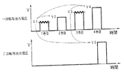
図5は以上述べてきた1次転写と2次転写のタイミングと出力電圧を示した図で矢印は定電流時に出力される電圧V1をもとに制御されることを示す。図6は実施例1の変形例であって1、3色目に定電流制御しそれらの値をもとに2、4色目および2次転写電圧を制御する。この場合も良好な転写性が環境や転写材サイズによらず確保できた。また、図7に示すように1色印字中に定電流制御から定電圧制御に切り換えることも可能であるが切り換え時にノイズがはいる場合があり図5、6に示すように非画像領域で定電流および定電圧制御の切り換えを行うのが望ましい。なお、図5から図7までは1次転写と2次転写が時間軸で重なる場合を示したので1次転写の最終色は定電圧制御であることが望ましい。1次転写の最終色が定電流制御で2次転写と同時にバイアスされると表面抵抗が、 105〜108Ωといった比較的低抵抗な中間転写体106を用いた場合、2次転写部における中間転写体106の電位が変動し転写ムラとなる場合があり好ましくない。
【0034】
画像領域の一部を定電流制御しその時の電圧にもとづき他の画像領域を定電圧制御する実施例としてはこれら図5〜7に限定されることはない。例えば、1、2色目は予め定められた電圧で定電圧制御、3色目は定電流制御としこの時に検知される電圧をもとに4色目を定電圧制御したり、逆に1色目を定電流制御としこの時に検知される電圧をもとに2色目を定電圧制御し、3、4色目は予め定められた電圧で定電圧制御してもよい。これらの場合も従来の色ごとに定められた電圧値を定電圧制御する方法に比べ良好な転写性が得られた。
【0035】
また、1次転写出力の1色目が定電流制御の時、連続印字時に2次転写出力と2枚目以降の1次転写出力の1色目が時間軸で重なる場合があり、先に述べた理由で転写不良をおこすことがある。そこで、1枚目の印字において本発明の制御(例えば図6に示す)を行い、2枚目以降の1、2色目は1枚目に決定される電圧V1、V2で定電圧制御し3色目は1枚目と同じく定電流制御し、4色目は定電圧制御することにより1次転写と2次転写が時間軸で重なるタイミングで定電圧制御が可能となり転写不良が防止される。この時、2枚目以降の1色目の電圧を前の印字の3色目の定電流制御時に検出される電圧にもとづいて定電圧制御してもよい。また、連続印字の場合に1枚目の印字において本発明の制御(例えば図5に示す)を行い、2枚目以降は1枚目に決定される電圧(V1、V2、V3、V4)で定電圧制御することが可能である。この方法は装置内の温湿度が大きく変化しない場合に有効である。
【0036】
尚、本発明に用いる中間転写体106としては、実施例中に述べたETFE以外にも、ポリフッカビニリデン、ポリカーボネイト、ポリエチレンテレフタレート等の基材にカーボン等の導電材を分散もしくは塗布することにより表面抵抗を中抵抗化(105〜1011Ω)したフィルム材を用いることができる。中間転写体106の周長は、装置が対応する最大転写材長さより長いことは勿論であり、感光体101の周長の整数倍であることが好ましい。
【0037】
(実施例2)
図8は本発明の画像形成装置における他の実施例の断面概観図である。実施例1と異なるのは、1次転写部と2次転写部の距離が最大画像長さより長く1次転写、2次転写が同時にバイアスされることがない点と1次転写用電源108、演算手段121の内部構成が簡略化されている点である。装置の動作および構成の説明は実施例1と同じであるため省略する。
【0038】
図9は1次転写と2次転写のタイミングと出力電圧を示した図で矢印は定電流時に出力される電圧V1をもとに制御されることを示す。1次転写と2次転写のバイアス印加タイミングが重ならない。よって2次転写時に中間転写体106の電位は一定に保たれるため1次転写のバイアス制御は定電流制御であっても画像に影響を及ぼすことはない。
【0039】
図10は実施例2に用いる1次転写用電源108、2次転写用電源117、演算手段121を示したものである。1次転写用電源108は定電流制御部402のみからなる。不図示の転写電圧出力要求信号が入ると定電流制御部402は電流i1(例えば10.0μA)の定電流バイアスを出力する。そのときの電圧をホールドし演算手段で扱える適当な電圧に変換し2次転写演算部405におくる。2次転写演算部405では実施例1に示した演算式にもとづき演算し2次転写用電源117の定電圧制御部406におくる。定電圧制御部406では2次転写演算部405から得た電圧をもとに出力電圧に増幅し2次転写出力する。以上の構成の電気回路はアナログ回路で設計できるが演算手段121での演算が複雑もしくはデータをROM化し読み出す構成ではA/D変換器、D/A変換器、マイクロプロセッサ等が必要となる。1次転写部が定電流制御でも図2に示したように実用可能範囲にあるため画像品質をさほど落とす事なく実施例1の構成に比べ1次転写電源108および演算手段121の低コスト化が可能となった。
【0040】
(実施例3)
装置構成は図1と同一であるため省略する。実施例1と異なる点は非画像領域で定電流制御し、その時の電圧を検知しその値をもとに画像領域を定電流制御する時の電流値を決定する点で1次転写用電源108の内部構成が異なる。
【0041】
図11は図2に加え非画像領域のV−I特性を示した図である。非画像領域にはトナーが存在しないため、画像領域に比べ見かけ上の抵抗は低く図に示すようにLL環境ではその差が大きく、HH環境ではその差が小さい。従来例で述べたように非画像領域で定電流制御し図中のL0、H0をもとに画像領域のバイアスを決定する従来の方法は最適バイアスとの誤差が大きく好ましくない。しかし、非画像領域で検知した電圧からおおよその環境を把握することはできる。そこで、1次転写用電源108は電流i0(例えば10.0μA)で定電流制御し、その時に検知した電圧をもとに画像部における定電流制御時の電流i1を決定する。例えば、検知した電圧が500V以下の時はHH環境と考えられるためi1=12μAとし、800V以上の時はLL環境と考えられるためi1=10μAとする。また、500〜800Vのときは常温常湿環境と考えられるのでi1=11μAとする。この方法で実施例1と同様に画像領域の一部を定電流制御し、他の画像領域をその時に検知した電圧にもとづき定電圧制御した結果を表4に示す。なお、演算手段121における式は実施例1と同じとした。
【0042】
【表4】
表2にくらべHH環境における最適電圧との差が減少した。実施例1に比べてより理想的なバイアス制御が可能となった。
【0044】
図12は実施例3における1次転写用電源108、2次転写用電源117、演算手段121を示したものである。1次転写用電源108は出力切り換え手段401、数水準の電流出力可能な定電流制御部407、定電圧制御部403、比較手段408からなる。不図示の転写電圧出力要求信号が入ると非画像領域において定電流制御部407は電流i0(例えば10.0μA)の定電流バイアスを出力する。その時の電圧を予め定めた値(例えば500V)と比較手段408にて比較する。比較手段408ではその結果にもとづいて定電流制御部407で出力すべき電流値の情報を与える(例えば500V以下では12μA)。定電流制御部407ではその情報にもとづき定電流バイアスi1(例えば12μA)を画像部に出力する。そのときの電圧をホールドし演算手段121で扱える適当な電圧に変換し1次転写演算部404および2次転写演算部405におくる。1次転写演算部404では、実施例1で示した演算式にもとづき演算し定電圧制御部403におくる。定電圧制御部403では1次転写演算部404から得た電圧をもとに出力電圧に増幅し出力切り換え手段401を切り換えて1次転写出力をする。2次転写演算部405でも実施例1で示した演算式にもとづき演算し2次転写用電源117の定電圧制御部406におくる。定電圧制御部406では2次転写演算部405から得た電圧をもとに出力電圧に増幅し2次転写出力する。以上の構成の電気回路はアナログ回路で設計できるが演算手段121での演算が複雑もしくはデータをROM化し読み出す構成ではA/D変換器、D/A変換器、マイクロプロセッサ等が必要となる。
【0045】
図13は以上述べてきた1次転写と2次転写のタイミングと出力電圧を示した図でVnは非画像領域を電流i0で定電流制御した時の電圧で、矢印はVnの値により決められた電流i1で画像領域を定電流制御した時に出力される電圧V1をもとに制御されることを示す。
【0046】
(実施例4)
図14は本発明の画像形成装置における他の実施例の断面概観図である。実施例1〜3との違いは転写材113を誘電体ドラム501に巻き付け転写材上で色重ねをする点である。
【0047】
まず、装置の動作を説明する。転写材113は、給紙カセット112から給紙手段111によりレジストローラ対114まで搬送されたのち、転写材担持体である誘電体ドラム501に転写材吸着用電源503がコロナ帯電器502に交流電圧を重畳した電圧を出力しその静電力により吸着される。帯電ローラ102は感光体101を均一にある電位(例えば−700V)に帯電する。レーザー走査光学系である露光手段103によって形成された600dpi(dot perinch)の解像度のレーザービームは折り返しミラー104により感光体101上に導かれ静電潜像(例えば−100V)が形成される。次に図中矢印方向に接離可能な一成分接触方式の現像器105の内、イエロー現像器105Yを接触させ他の現像器は離間させるとともに不図示の電源の電界の作用によって負帯電性イエロートナーが反転現像され感光体上101において顕像化される。顕像化されたイエロートナーは、PET(ポリエチレンテレフタレート)等の誘電体ドラム501上に吸着された転写材113上に導電性ブレード504にトナーと逆極性のバイアスが転写用電源505より印加されその電界の作用により転写される。感光体101上の転写残りトナーは、ブレードを接触させてクリーニングする感光体クリーナー109で回収され、続いて感光体電位は除電ランプ110によりリセットされる。同様の動作を誘電体ドラム501の位置と露光手段103の発光タイミングの同期を取りマゼンタ現像器105M、シアン現像器105C、ブラック現像器105Kについても繰り返すことにより、誘電ドラム501に吸着された転写材113上に各色のトナーが重ねられフルカラー画像が形成される。フルカラー画像が形成された転写材113は、除電用電源507からコロナ帯電器506に印加される交流重畳した電界の作用により誘電体ドラム501から除電、剥離された後、転写材搬送ベルト508により搬送され定着手段120にて定着後装置外に排出される。
【0048】
次に転写用電源505のバイアス制御方法について詳述する。
【0049】
図15は転写部における低温、低湿(以後LL環境と呼ぶ)及び高温、高湿環境(HH環境と呼ぶ)下におけるベタ画像のV−I特性を示したもので斜線部内が転写が良好にされる実用範囲(転写効率で80%以上)である。LL環境とHH環境でこのようにV−I特性が異なるのは誘電体ドラム501、トナー、転写材113の抵抗値およびトナーの帯電量が環境で変化するためである。図中の○印は転写部で放電が開始する直前の点を示し、この点で最大転写効率(転写効率で90〜97%)をとる。したがってこの○印となるように転写用電源505が制御されれば最高品質画像が得られる。転写用電源505を定電流制御しその値をi1とすればLL、HH環境で転写電圧は図に示すようにL1、L2..、H1、H2..となり実用範囲内にははいるが最大転写効率を得るという観点からはLL環境の3、4色目で最適電圧(L1max、L2max..、H1max、H2max..)からずれる。具体例としてプロセス速度130mm/s、誘電体ドラム501の表面抵抗がLLで1015Ω、HHで1014Ω、転写材113として表面抵抗がLLで1010Ω、HHで107Ωの紙を用い、トナーの帯電量がLLで20μC/g、HHで12μC/gの時、i1=10.0μAとし定電流時に出力される電圧および最大転写効率を得る最適電圧を調べ表5に示す。
【0050】
【表5】
表5からLL環境の3色目、4色目で最適転写電圧との差が大きいことがわかる。そこで、1色目は定電流制御しその時に出力される電圧値にもとづいて2、3、4色目を定電圧制御した。具体的には演算手段509において、1色目の定電流制御時に出力される電圧をV1、2色目以降の定電圧制御時に出力する電圧をV2、V3、V4とすると、V2=V1+1/4×V1−300、V3=V2+1/4×V1−300、V4=V3+1/4×V1−300とする。
【0052】
この方法にもとづいてバイアス制御を行った結果を表6に示す。
【0053】
【表6】
このように画像領域の一部(本実施例では第1色目)を定電流制御しその時に出力される電圧(V1)をもとに他の画像領域(本実施例では第2、3、4色目)における電圧(V2、V3、V4)を定めることにより最適転写電圧に制御可能となった。
【0055】
図16は以上述べてきた転写用電源505と除電用電源507の出力タイミングと出力電圧を示した図で矢印は定電流時に出力される電圧V1をもとに制御されることを示す。図17は実施例4の変形例であって1、3色目に定電流制御しそれらの値をもとに2、4色目の転写電圧を制御する。この場合も良好な転写性が環境や転写材サイズによらず確保できた。また、図18に示すように1色印字中に定電流制御から定電圧制御に切り換えることも可能であるが切り換え時にノイズがはいる場合があり図13、14に示すように非画像領域で定電流および定電圧制御の切り換えを行うのが望ましい。なお、図16から図18までは転写用電源505と除電用電源507の出力が時間軸で重なる場合を示したので転写部の最終色は定電圧制御であることが望ましい。転写用電源505の最終色が定電流制御で除電用電源507と同時にバイアスされると誘電体ドラム501の表面抵抗によっては転写部における誘電体ドラム501の電位が変動し転写ムラとなる場合があり好ましくない。
【0056】
以上、4つの実施例を用いて本発明を説明したが発明の主旨は画像領域の一部を定電流制御しその時に出力される電圧にもとづいて他の画像領域に印加する電圧を決定するものであり、実施形態はこれら実施例に限られるものではない。
【0057】
【発明の効果】
以上述べてきた本発明は以下の効果を有する。
【0058】
請求項1記載の発明によれば、1次転写で画像領域の一部で定電流制御することによりトナーも含めた負荷抵抗がわかり、その値をもとに最適転写電圧を印加するため中間転写体やトナーの抵抗値等が変動しても高品質なカラー画像形成装置を提供できる。
【0059】
請求項2記載の発明によれば、1次転写の定電流制御と定電圧制御の切り換えを非画像領域で行うため制御切り換え時の電気的ノイズが画像に影響を及ぼすことがなく高品質なカラー画像形成装置を提供できる。
【0060】
請求項3記載の発明によれば、1次転写と2次転写が時間軸で重なるタイミングで1次転写用電源を定電圧制御するため中間転写体が一定電位となる。よって2次転写時の電界強度が変動することがないため高品質なカラー画像形成装置を提供できる。
【0061】
請求項4、5記載の発明によれば、1次転写で画像領域の一部で定電流制御する時の1次転写用電源の出力電圧を検知し、その検知された1次転写用電源の出力電圧をもとに2次転写における電圧を決定するため転写材抵抗や転写材幅によらず高品質なカラー画像形成装置を提供できる。
【0062】
請求項6記載の発明によれば、1次転写用電源で非画像領域において定電流制御しその時に検知される1次転写用電源の出力電圧にもとづき画像領域の一部を最適な電流値で定電流制御するためさらに精度の高い制御が可能となり高品質なカラー画像形成装置を提供できる。
【0063】
請求項7記載の発明によれば、転写部の画像領域の一部で定電流制御する時の転写用電源の出力電圧を検知し、その検知された転写用電源の出力電圧をもとに定電圧値を決定するため転写材抵抗や転写材幅によらず高品質なカラー画像形成装置を提供できる。
【0064】
請求項8記載の発明によれば、転写部の定電流制御と定電圧制御の切り換えを非画像領域で行うことにより切り換え時の電気的ノイズが画像に影響を及ぼすことはなく高品質なカラー画像形成装置を提供できる。
【0065】
請求項9記載の発明によれば、転写と除電が時間軸で重なるタイミングで転写用電源を定電圧制御するため転写位置の電位が一定電位となる。よって転写部の電界強度が除電電流で変動することなく高品質なカラー画像形成装置を提供できる。
【図面の簡単な説明】
【図1】第1の実施例におけるカラー画像形成装置の断面概観図。
【図2】第1の実施例における1次転写部の電圧−電流特性を示す図。
【図3】第1の実施例における2次転写部の電圧−電流特性を示す図。
【図4】第1の実施例における1次転写用電源、2次転写用電源、および演算手段の説明をする図。
【図5】第1の実施例における1次転写及び2次転写の出力タイミングおよび電圧を示す図。
【図6】第1の実施例の変形例における1次転写及び2次転写の出力タイミングおよび電圧を示す図。
【図7】第1の実施例の変形例における1次転写及び2次転写の出力タイミングおよび電圧を示す図。
【図8】第2の実施例におけるカラー画像形成装置の断面概観図。
【図9】第2の実施例における1次転写及び2次転写の出力タイミングおよび電圧を示す図。
【図10】第2の実施例における1次転写用電源、2次転写用電源、および演算手段の説明をする図。
【図11】第3の実施例における1次転写部の画像部および非画像部における電圧−電流特性を示す図。
【図12】第3の実施例における1次転写用電源、2次転写用電源、および演算手段の説明をする図。
【図13】第3の実施例における1次転写及び2次転写の出力タイミングおよび電圧を示す図。
【図14】第4の実施例における画像形成装置断面概観図。
【図15】第4の実施例における転写時の電圧−電流特性を示す図。
【図16】第4の実施例における転写部及び除電部の出力タイミングおよび電圧を示す図。
【図17】第4の実施例の変形例における転写部及び除電部の出力タイミングおよび電圧を示す図。
【図18】第4の実施例の変形例における転写部及び除電部の出力タイミングおよび電圧を示す図。
【符号の説明】
101 感光体
102 帯電ローラ
103 露光手段
104 折り返しミラー
105Y イエロー現像器
105M マゼンタ現像器
105C シアン現像器
105K ブラック現像器
106 中間転写体
107 1次転写ローラ
108 1次転写用電源
109 感光体クリーナー
110 除電ランプ
111 給紙手段
112 給紙カセット
113 転写材
114 レジストローラ対
115 駆動ローラ
116 2次転写ローラ
117 2次転写用電源
118 テンションローラ
119 中間転写体クリーナー
120 定着手段
121 演算手段
501 誘電体ドラム
502 コロナ帯電器
503 転写材吸着用電源
504 導電性ブレード
505 転写用電源
506 コロナ帯電器
507 除電用電源
508 転写材搬送ベルト
509 演算手段[0001]
[Industrial application fields]
The present invention relates to an apparatus for forming an image using an electrophotographic process, and more particularly to an image forming apparatus suitable for constituting a color electrophotographic process using electrostatic transfer.
[0002]
[Prior art]
Many image forming apparatuses using a color electrophotographic process, and in particular, a bias control method and apparatus related to a transfer process have been proposed. The following three are typical image forming apparatuses.
[0003]
(1) In Japanese Patent Application Laid-Open No. 2-287380, etc., a constant current control is performed in a non-image area, a voltage at that time is held, and a constant voltage control is performed in an image area. It was said that sex could be secured.
[0004]
(2) In Japanese Patent Laid-Open No. 6-295132, a bias control method for a primary transfer unit for transferring toner from a photosensitive member to an intermediate transfer member is defined in an apparatus for superimposing colors on an intermediate transfer member and transferring them to a transfer material. According to the current control, a transfer failure at the time of color superposition can be prevented.
[0005]
(3) In Japanese Patent Publication No. 63-7386, in a process of winding a paper around a dielectric drum and sequentially transferring a color toner image, it is said that a high-quality transfer image can be obtained by increasing the transfer voltage in the transfer order.
[0006]
[Problems to be solved by the invention]
However, the prior art has the following problems.
[0007]
First, in the technique (1), a non-image area (an area where no toner is present on the photoconductor) is subjected to constant current control, and an image area (toner can be present on the photoconductor). Therefore, a color image forming apparatus that has a large error with respect to the optimum voltage and requires accuracy is not sufficient.
[0008]
Next, as for the technique (2), in a system using an intermediate transfer member, bias may be applied simultaneously at a plurality of locations. At this time, if the primary transfer portion is under constant current control, the potential of the intermediate transfer member varies according to the impedance of the primary transfer portion. As a result, there is a problem in that the electric field strength in the secondary transfer in which the toner is transferred from the intermediate transfer member to the transfer material becomes unstable, transferability is impaired, and the quality on the transfer material as the final image is deteriorated. In the secondary transfer portion, resistance varies by several orders of magnitude depending on the environment, and high-efficiency transfer is required for transfer materials having various sizes in the width direction. Sufficient transferability could not be secured with a power supply or a constant current power supply with a fixed current.
[0009]
In the technique (3), since a constant voltage value is fixed for each color, a transfer current is insufficient in a high resistance paper such as an OHP sheet or a paper in a low humidity environment, which may cause a transfer failure. In order to avoid this problem, it has also been proposed to use a constant current control for the transfer portion. However, since a high-resistance dielectric drum is used as the transfer material carrier, it is necessary to have static elimination means that superimposes AC voltage in order to remove residual charges, and the transfer current is interfered with the static elimination current at the timing when static elimination and transfer occur simultaneously. In some cases, the current involved in the toner movement is not secured and a good image cannot be obtained.
[0010]
Therefore, an object of the present invention is to provide a system using an intermediate transfer member,
(1) The image quality is stabilized even if the resistance value of the intermediate transfer member and the toner charge amount fluctuate in the environment at the primary transfer portion. (2) The resistance value of the intermediate transfer member and transfer material at the secondary transfer portion. (3) primary transfer, secondary transfer bias, and transfer defects that occur at the same time when the secondary transfer bias is applied simultaneously are resolved. In addition, in a system in which a transfer material is carried on a transfer material carrier and color superposition is performed, (4) the image quality is stabilized even if the resistance value of the transfer material fluctuates, and (5) transfer and static elimination bias are simultaneously performed. This is to solve a transfer failure that occurs at the timing of application.
[0011]
[Means for Solving the Problems]
The color image forming apparatus of the present invention includes a primary transfer power source for sequentially transferring a color toner image visualized on a photosensitive member onto an intermediate transfer member, and a color toner image superimposed on the intermediate transfer member. In a color image forming apparatus provided with a secondary transfer power source for collectively transferring images onto a transfer material, the primary transfer power source is controlled at a constant current in a part of the image area. Output of the primary transfer power supply Detect voltage and in other image areas Said Detected Output of power supply for primary transfer It is characterized by constant voltage control based on the voltage.
[0012]
[Action]
According to the first aspect of the present invention, the load resistance including the toner can be determined by controlling the constant current in a part of the image area in the primary transfer, and the intermediate transfer is performed to apply the optimum transfer voltage based on the value. A stable quality image can be obtained even if the resistance value of the body or toner fluctuates.
[0013]
According to the second aspect of the present invention, the switching between the primary transfer constant current control and the constant voltage control is performed in the non-image region, so that electrical noise at the time of switching the control does not affect the image.
[0014]
According to the third aspect of the present invention, since the primary transfer power source is controlled at a constant voltage at the timing at which the primary transfer and the secondary transfer overlap on the time axis, the intermediate transfer member becomes a constant potential. Therefore, the image quality is stabilized without fluctuation of the electric field intensity at the time of secondary transfer.
[0015]
According to the fourth and fifth aspects of the present invention, the constant current control is performed in a part of the image area in the primary transfer. Output of power supply for primary transfer Detected voltage and detected Output of power supply for primary transfer Since the voltage in the secondary transfer is determined based on the voltage, good transferability is ensured regardless of the transfer material resistance and the transfer material width.
[0016]
According to the sixth aspect of the present invention, constant current control is performed in the non-image area by the primary transfer power source, and detection is performed at that time. Output of power supply for primary transfer Since a part of the image area is controlled at a constant current with an optimum current value based on the voltage, control with higher accuracy is possible.
[0017]
According to the seventh aspect of the present invention, the constant current control is performed in a part of the image area of the transfer portion. Output of power supply for transfer Detected voltage and detected Output of power supply for transfer Since the constant voltage value is determined based on the voltage, good transferability is ensured regardless of the transfer material resistance and the transfer material width.
[0018]
According to the eighth aspect of the present invention, the switching between the constant current control and the constant voltage control of the transfer portion is performed in the non-image region, so that the electric noise at the time of switching does not affect the image.
[0019]
According to the ninth aspect of the invention, since the transfer power source is controlled at a constant voltage at the timing at which transfer and charge removal overlap on the time axis, the potential at the transfer position becomes a constant potential. Therefore, the image quality is stabilized without the electric field strength of the transfer portion being changed by the static elimination current.
[0020]
【Example】
Hereinafter, Claims 1 to 4 are (Example 1), Claim 5 is (Example 2), Claim 6 is (Example 3), and Claims 7 to 9 are (Example 4). Will be described.
[0021]
(Example 1)
FIG. 1 is a schematic cross-sectional view of a color image forming apparatus of the present invention.
[0022]
First, the operation of the apparatus will be described. The charging
[0023]
Next, a bias control method for primary transfer and secondary transfer will be described in detail.
[0024]
FIG. 2 shows voltage-current characteristics (hereinafter referred to as VI characteristics) of a solid image in a primary transfer portion under low temperature, low humidity (hereinafter referred to as LL environment) and high temperature and high humidity environment (referred to as HH environment). In the figure, the shaded area is a practical range where transfer is good (transfer efficiency is 80% or more). The reason why the VI characteristics are greatly different between the LL environment and the HH environment is that the resistance value of the
[0025]
[Table 1]
It can be seen from Table 1 that the difference from the optimum transfer voltage is large for the third and fourth colors in the LL environment. Therefore, constant current control was performed for the first color, and constant voltage control was performed for the second, third, and fourth colors based on the voltage value output at that time. Specifically, in the calculation means 121, assuming that the voltage output during the constant current control for the first color is V1, and the voltages output during the constant voltage control for the second and subsequent colors are V2, V3, and V4, V2 = V1 + 2/9 × V1. V3 = V2 + 2/9 × V1, and V4 = V3 + 2/9 × V1. Table 2 shows the result of bias control based on this method.
[0027]
[Table 2]
In this way, a part of the image area (first color in the present embodiment) is subjected to constant current control, and another image area (second, third, fourth, in this embodiment) is based on the voltage (V1) output at that time. By determining the voltage (V2, V3, V4) in the color), it becomes possible to control the optimum transfer voltage.
[0029]
FIG. 3 shows the VI characteristics when the
[0030]
[Table 3]
From this result, assuming that the output at the constant current in the primary transfer is V1 (V), and the voltage that takes the maximum transfer efficiency in the secondary transfer is V0 (V), there is a relationship of V0 = 32/9 × V1-800. I understand. Therefore, a good image can be obtained by performing this calculation by the calculation means 121 and performing constant voltage control of the secondary transfer at V0. In this equation, V0 may be 0 or less, but 0V is output at that time.
[0032]
FIG. 4 shows the primary
[0033]
FIG. 5 is a diagram showing the timing and output voltage of the primary transfer and the secondary transfer described above, and the arrows indicate that the control is based on the voltage V1 output at a constant current. FIG. 6 shows a modification of the first embodiment, in which constant current control is performed for the first and third colors, and the second, fourth color, and secondary transfer voltage are controlled based on these values. Also in this case, good transferability could be ensured regardless of the environment and the transfer material size. In addition, it is possible to switch from constant current control to constant voltage control during single color printing as shown in FIG. 7, but there may be noise at the time of switching, as shown in FIGS. It is desirable to switch between current and constant voltage control. 5 to 7 show the case where the primary transfer and the secondary transfer overlap on the time axis, it is desirable that the final color of the primary transfer is constant voltage control. When the final color of the primary transfer is biased simultaneously with the secondary transfer by constant current control, the surface resistance is 10 5 -10 8 When the
[0034]
Embodiments in which a part of the image area is controlled with constant current and the other image areas are controlled with constant voltage based on the voltage at that time are not limited to those shown in FIGS. For example, the first and second colors are controlled at a constant voltage with a predetermined voltage, the third color is controlled at a constant current, and the fourth color is controlled at a constant voltage based on the voltage detected at this time, or the first color is controlled at a constant current. For control, the second color may be controlled at a constant voltage based on the voltage detected at this time, and the third and fourth colors may be controlled at a predetermined voltage. Also in these cases, better transferability was obtained as compared with the conventional method in which the voltage value determined for each color was controlled at a constant voltage.
[0035]
In addition, when the first color of the primary transfer output is constant current control, the secondary transfer output and the first color of the first and subsequent primary transfer outputs may overlap on the time axis during continuous printing. May cause transfer failure. Therefore, the control of the present invention (for example, shown in FIG. 6) is performed on the first sheet, and the first and second colors after the second sheet are controlled at a constant voltage with the voltages V1 and V2 determined on the first sheet. As in the first sheet, constant current control is performed, and in the fourth color, constant voltage control is performed, so that constant voltage control can be performed at the timing at which primary transfer and secondary transfer overlap on the time axis, thereby preventing transfer failure. At this time, the voltage of the first color after the second sheet may be controlled at a constant voltage based on the voltage detected during the constant current control of the third color of the previous printing. In the case of continuous printing, the control of the present invention (for example, shown in FIG. 5) is performed for the first printing, and the voltages determined for the first and subsequent sheets (V1, V2, V3, V4) are used for the second and subsequent sheets. Constant voltage control is possible. This method is effective when the temperature and humidity in the apparatus do not change greatly.
[0036]
In addition to the ETFE described in the examples, the
[0037]
(Example 2)
FIG. 8 is a schematic cross-sectional view of another embodiment of the image forming apparatus of the present invention. The difference from the first embodiment is that the distance between the primary transfer portion and the secondary transfer portion is longer than the maximum image length, and the primary transfer and the secondary transfer are not biased at the same time. The internal configuration of the
[0038]
FIG. 9 is a diagram showing the timing of the primary transfer and the secondary transfer and the output voltage, and the arrows indicate that the control is based on the voltage V1 output at a constant current. The bias application timings of primary transfer and secondary transfer do not overlap. Therefore, since the potential of the
[0039]
FIG. 10 shows the primary
[0040]
(Example 3)
The apparatus configuration is the same as that shown in FIG. A difference from the first embodiment is that the constant current control is performed in the non-image area, the voltage at that time is detected, and the current value when the constant current control is performed on the image area is determined based on the detected voltage. The internal configuration is different.
[0041]
FIG. 11 is a diagram showing the VI characteristics of the non-image area in addition to FIG. Since there is no toner in the non-image area, the apparent resistance is lower than that in the image area, and the difference is large in the LL environment and small in the HH environment as shown in the figure. As described in the conventional example, the conventional method of controlling the constant current in the non-image region and determining the bias of the image region based on L0 and H0 in the figure is not preferable because of an error with the optimum bias. However, the approximate environment can be grasped from the voltage detected in the non-image area. Therefore, the primary
[0042]
[Table 4]
Compared to Table 2, the difference from the optimum voltage in the HH environment was reduced. Compared to the first embodiment, more ideal bias control is possible.
[0044]
FIG. 12 shows the primary
[0045]
FIG. 13 is a diagram showing the timing and output voltage of the primary transfer and the secondary transfer described above. Vn is a voltage when the non-image area is controlled with constant current i0, and the arrow is determined by the value of Vn. It shows that the image area is controlled based on the voltage V1 output when the constant current control is performed on the image area with the current i1.
[0046]
(Example 4)
FIG. 14 is a schematic cross-sectional view of another embodiment of the image forming apparatus of the present invention. The difference from the first to third embodiments is that the
[0047]
First, the operation of the apparatus will be described. After the
[0048]
Next, a bias control method for the
[0049]
FIG. 15 shows the VI characteristics of a solid image under low temperature, low humidity (hereinafter referred to as LL environment) and high temperature, high humidity environment (referred to as HH environment) in the transfer portion. Practical range (80% or more in transfer efficiency). The reason why the VI characteristics are different between the LL environment and the HH environment is that the resistance values of the
[0050]
[Table 5]
From Table 5, it can be seen that there is a large difference from the optimum transfer voltage in the third and fourth colors of the LL environment. Therefore, constant current control was performed for the first color, and constant voltage control was performed for the second, third, and fourth colors based on the voltage value output at that time. Specifically, in the calculation means 509, assuming that the voltage output during the constant current control for the first color is V1, and the voltages output during the constant voltage control for the second and subsequent colors are V2, V3, and V4, V2 = V1 + 1/4 × V1. −300, V3 = V2 + 1/4 × V1-300, and V4 = V3 + 1/4 × V1-300.
[0052]
Table 6 shows the result of bias control based on this method.
[0053]
[Table 6]
In this way, a part of the image area (first color in the present embodiment) is subjected to constant current control, and another image area (second, third, fourth, in this embodiment) is based on the voltage (V1) output at that time. By determining the voltage (V2, V3, V4) in the color), it becomes possible to control the optimum transfer voltage.
[0055]
FIG. 16 is a diagram showing the output timing and output voltage of the
[0056]
Although the present invention has been described with reference to the four embodiments, the gist of the invention is that constant current control is performed on a part of the image area, and the voltage applied to the other image area is determined based on the voltage output at that time. The embodiments are not limited to these examples.
[0057]
【The invention's effect】
The present invention described above has the following effects.
[0058]
According to the first aspect of the present invention, the load resistance including the toner can be determined by controlling the constant current in a part of the image area in the primary transfer, and the intermediate transfer is performed to apply the optimum transfer voltage based on the value. A high-quality color image forming apparatus can be provided even when the resistance value of the body and toner fluctuates.
[0059]
According to the second aspect of the present invention, since the switching between the constant current control and the constant voltage control of the primary transfer is performed in the non-image area, the electrical noise at the time of switching the control does not affect the image and the color is high quality. An image forming apparatus can be provided.
[0060]
According to the third aspect of the present invention, since the primary transfer power source is controlled at a constant voltage at the timing at which the primary transfer and the secondary transfer overlap on the time axis, the intermediate transfer member becomes a constant potential. Therefore, since the electric field strength at the time of secondary transfer does not fluctuate, a high-quality color image forming apparatus can be provided.
[0061]
According to the fourth and fifth aspects of the present invention, the constant current control is performed in a part of the image area in the primary transfer. Output of power supply for primary transfer Detected voltage and detected Output of power supply for primary transfer Since the voltage in the secondary transfer is determined based on the voltage, a high-quality color image forming apparatus can be provided regardless of the transfer material resistance and the transfer material width.
[0062]
According to the sixth aspect of the present invention, constant current control is performed in the non-image area by the primary transfer power source, and detection is performed at that time. Output of power supply for primary transfer Since a part of the image area is controlled at a constant current with an optimum current value based on the voltage, more accurate control is possible, and a high-quality color image forming apparatus can be provided.
[0063]
According to the seventh aspect of the present invention, the constant current control is performed in a part of the image area of the transfer portion. Output of power supply for transfer Detected voltage and detected Output of power supply for transfer Since the constant voltage value is determined based on the voltage, a high-quality color image forming apparatus can be provided regardless of the transfer material resistance and the transfer material width.
[0064]
According to the eighth aspect of the present invention, the switching between the constant current control and the constant voltage control of the transfer portion is performed in the non-image region, so that the electrical noise at the time of switching does not affect the image and the high quality color image. A forming apparatus can be provided.
[0065]
According to the ninth aspect of the invention, since the transfer power source is controlled at a constant voltage at the timing at which transfer and charge removal overlap on the time axis, the potential at the transfer position becomes a constant potential. Therefore, a high-quality color image forming apparatus can be provided without the electric field strength of the transfer portion being changed by the static elimination current.
[Brief description of the drawings]
FIG. 1 is a schematic cross-sectional view of a color image forming apparatus according to a first embodiment.
FIG. 2 is a graph showing voltage-current characteristics of a primary transfer portion in the first embodiment.
FIG. 3 is a diagram illustrating voltage-current characteristics of a secondary transfer portion in the first embodiment.
FIG. 4 is a diagram illustrating a primary transfer power source, a secondary transfer power source, and a calculation unit in the first embodiment.
FIG. 5 is a diagram illustrating output timing and voltage of primary transfer and secondary transfer in the first embodiment.
FIG. 6 is a diagram illustrating output timings and voltages of primary transfer and secondary transfer in a modification of the first embodiment.
FIG. 7 is a diagram showing output timing and voltage of primary transfer and secondary transfer in a modification of the first embodiment.
FIG. 8 is a schematic cross-sectional view of a color image forming apparatus according to a second embodiment.
FIG. 9 is a diagram illustrating the output timing and voltage of primary transfer and secondary transfer in the second embodiment.
FIG. 10 is a diagram illustrating a primary transfer power source, a secondary transfer power source, and a calculation unit according to a second embodiment.
FIG. 11 is a diagram illustrating voltage-current characteristics in an image portion and a non-image portion of a primary transfer portion in a third embodiment.
FIG. 12 is a diagram illustrating a primary transfer power source, a secondary transfer power source, and a calculation unit according to a third embodiment.
FIG. 13 is a diagram showing the output timing and voltage of primary transfer and secondary transfer in the third embodiment.
FIG. 14 is a schematic cross-sectional view of an image forming apparatus according to a fourth embodiment.
FIG. 15 is a diagram showing voltage-current characteristics during transfer in a fourth embodiment.
FIG. 16 is a diagram illustrating output timings and voltages of a transfer unit and a charge removal unit in a fourth embodiment.
FIG. 17 is a diagram illustrating output timings and voltages of a transfer unit and a charge removal unit in a modification of the fourth embodiment.
FIG. 18 is a diagram illustrating output timings and voltages of a transfer unit and a charge removal unit in a modification of the fourth embodiment.
[Explanation of symbols]
101 photoconductor
102 Charging roller
103 Exposure means
104 Folding mirror
105Y Yellow developer
105M Magenta developer
105C cyan developer
105K black developer
106 Intermediate transfer member
107 Primary transfer roller
108 Power supply for primary transfer
109 Photoconductor cleaner
110 Static elimination lamp
111 Paper feeding means
112 Paper cassette
113 Transfer material
114 Registration roller pair
115 Drive roller
116 Secondary transfer roller
117 Power supply for secondary transfer
118 Tension roller
119 Intermediate transfer cleaner
120 fixing means
121 Calculation means
501 Dielectric drum
502 Corona charger
503 Power supply for transfer material adsorption
504 conductive blade
505 Power supply for transfer
506 Corona charger
507 Power supply for static elimination
508 Transfer material conveying belt
509 Calculation means
Claims (9)
Priority Applications (1)
| Application Number | Priority Date | Filing Date | Title |
|---|---|---|---|
| JP16055295A JP3620548B2 (en) | 1995-06-27 | 1995-06-27 | Color image forming apparatus |
Applications Claiming Priority (1)
| Application Number | Priority Date | Filing Date | Title |
|---|---|---|---|
| JP16055295A JP3620548B2 (en) | 1995-06-27 | 1995-06-27 | Color image forming apparatus |
Publications (2)
| Publication Number | Publication Date |
|---|---|
| JPH0915999A JPH0915999A (en) | 1997-01-17 |
| JP3620548B2 true JP3620548B2 (en) | 2005-02-16 |
Family
ID=15717465
Family Applications (1)
| Application Number | Title | Priority Date | Filing Date |
|---|---|---|---|
| JP16055295A Expired - Fee Related JP3620548B2 (en) | 1995-06-27 | 1995-06-27 | Color image forming apparatus |
Country Status (1)
| Country | Link |
|---|---|
| JP (1) | JP3620548B2 (en) |
Families Citing this family (4)
| Publication number | Priority date | Publication date | Assignee | Title |
|---|---|---|---|---|
| US6408158B1 (en) | 1997-01-31 | 2002-06-18 | Seiko Epson Corporation | Intermediate transfer unit |
| US6856782B2 (en) | 1997-01-31 | 2005-02-15 | Seiko Epson Corporation | Intermediate transfer unit having a primary and a secondary transfer member |
| EP0856783B1 (en) * | 1997-01-31 | 2002-04-17 | Seiko Epson Corporation | Recording Medium Carrier System |
| JP6504111B2 (en) * | 2016-05-26 | 2019-04-24 | 京セラドキュメントソリューションズ株式会社 | Image forming device |
-
1995
- 1995-06-27 JP JP16055295A patent/JP3620548B2/en not_active Expired - Fee Related
Also Published As
| Publication number | Publication date |
|---|---|
| JPH0915999A (en) | 1997-01-17 |
Similar Documents
| Publication | Publication Date | Title |
|---|---|---|
| EP1014218B1 (en) | Method and apparatus for image forming performing cleaning and discharging operations on image forming members | |
| US5983060A (en) | Image forming apparatus which removes a surface potential of an intermediate transfer member | |
| JP3718045B2 (en) | Image forming apparatus | |
| US5287144A (en) | Image forming apparatus having transfer charger which is controlled according to ambient conditions | |
| JPH10274892A (en) | Image forming device | |
| US5187536A (en) | Image forming apparatus | |
| KR100305164B1 (en) | Image forming apparatus with intermediate transfer member | |
| JP2004086166A (en) | Image forming apparatus | |
| JP3620548B2 (en) | Color image forming apparatus | |
| JP2002072609A (en) | Image forming device | |
| US5049934A (en) | Image forming apparatus having image transfer means | |
| JP4255709B2 (en) | Image forming apparatus and transfer material jam detection method thereof | |
| JP3781070B2 (en) | Color image forming apparatus | |
| JP2002333779A (en) | Image forming apparatus | |
| JP3358326B2 (en) | High voltage power supply and image forming apparatus | |
| JPH0786727B2 (en) | Recording sheet transport device | |
| JP2795048B2 (en) | Electrophotographic recording device | |
| JPH0425885A (en) | Transfer device | |
| JPH06295132A (en) | Image forming device | |
| JP3613293B2 (en) | Image forming apparatus | |
| JP2711903B2 (en) | Image forming device | |
| JP3130700B2 (en) | Electrophotographic recording device | |
| JP3611270B2 (en) | Image forming apparatus | |
| JP3317224B2 (en) | Electrophotographic recording device | |
| JP2002372834A (en) | Color image forming equipment |
Legal Events
| Date | Code | Title | Description |
|---|---|---|---|
| A131 | Notification of reasons for refusal |
Free format text: JAPANESE INTERMEDIATE CODE: A131 Effective date: 20040810 |
|
| RD02 | Notification of acceptance of power of attorney |
Free format text: JAPANESE INTERMEDIATE CODE: A7422 Effective date: 20040901 |
|
| A521 | Request for written amendment filed |
Free format text: JAPANESE INTERMEDIATE CODE: A523 Effective date: 20040929 |
|
| TRDD | Decision of grant or rejection written | ||
| A01 | Written decision to grant a patent or to grant a registration (utility model) |
Free format text: JAPANESE INTERMEDIATE CODE: A01 Effective date: 20041027 |
|
| A61 | First payment of annual fees (during grant procedure) |
Free format text: JAPANESE INTERMEDIATE CODE: A61 Effective date: 20041109 |
|
| R150 | Certificate of patent or registration of utility model |
Free format text: JAPANESE INTERMEDIATE CODE: R150 |
|
| FPAY | Renewal fee payment (event date is renewal date of database) |
Free format text: PAYMENT UNTIL: 20081126 Year of fee payment: 4 |
|
| FPAY | Renewal fee payment (event date is renewal date of database) |
Free format text: PAYMENT UNTIL: 20091126 Year of fee payment: 5 |
|
| FPAY | Renewal fee payment (event date is renewal date of database) |
Free format text: PAYMENT UNTIL: 20091126 Year of fee payment: 5 |
|
| FPAY | Renewal fee payment (event date is renewal date of database) |
Free format text: PAYMENT UNTIL: 20101126 Year of fee payment: 6 |
|
| FPAY | Renewal fee payment (event date is renewal date of database) |
Free format text: PAYMENT UNTIL: 20101126 Year of fee payment: 6 |
|
| FPAY | Renewal fee payment (event date is renewal date of database) |
Free format text: PAYMENT UNTIL: 20111126 Year of fee payment: 7 |
|
| LAPS | Cancellation because of no payment of annual fees |