JP3576859B2 - Light emitting device and system using the same - Google Patents
Light emitting device and system using the same Download PDFInfo
- Publication number
- JP3576859B2 JP3576859B2 JP7507099A JP7507099A JP3576859B2 JP 3576859 B2 JP3576859 B2 JP 3576859B2 JP 7507099 A JP7507099 A JP 7507099A JP 7507099 A JP7507099 A JP 7507099A JP 3576859 B2 JP3576859 B2 JP 3576859B2
- Authority
- JP
- Japan
- Prior art keywords
- light
- light emitting
- photonic crystal
- crystal structure
- emitting device
- Prior art date
- Legal status (The legal status is an assumption and is not a legal conclusion. Google has not performed a legal analysis and makes no representation as to the accuracy of the status listed.)
- Expired - Fee Related
Links
Images


Classifications
-
- G—PHYSICS
- G02—OPTICS
- G02B—OPTICAL ELEMENTS, SYSTEMS OR APPARATUS
- G02B6/00—Light guides; Structural details of arrangements comprising light guides and other optical elements, e.g. couplings
- G02B6/10—Light guides; Structural details of arrangements comprising light guides and other optical elements, e.g. couplings of the optical waveguide type
- G02B6/12—Light guides; Structural details of arrangements comprising light guides and other optical elements, e.g. couplings of the optical waveguide type of the integrated circuit kind
- G02B6/122—Basic optical elements, e.g. light-guiding paths
- G02B6/1225—Basic optical elements, e.g. light-guiding paths comprising photonic band-gap structures or photonic lattices
-
- B—PERFORMING OPERATIONS; TRANSPORTING
- B82—NANOTECHNOLOGY
- B82Y—SPECIFIC USES OR APPLICATIONS OF NANOSTRUCTURES; MEASUREMENT OR ANALYSIS OF NANOSTRUCTURES; MANUFACTURE OR TREATMENT OF NANOSTRUCTURES
- B82Y20/00—Nanooptics, e.g. quantum optics or photonic crystals
-
- H—ELECTRICITY
- H01—ELECTRIC ELEMENTS
- H01J—ELECTRIC DISCHARGE TUBES OR DISCHARGE LAMPS
- H01J63/00—Cathode-ray or electron-stream lamps
- H01J63/02—Details, e.g. electrode, gas filling, shape of vessel
- H01J63/04—Vessels provided with luminescent coatings; Selection of materials for the coatings
-
- H—ELECTRICITY
- H01—ELECTRIC ELEMENTS
- H01K—ELECTRIC INCANDESCENT LAMPS
- H01K1/00—Details
- H01K1/02—Incandescent bodies
- H01K1/04—Incandescent bodies characterised by the material thereof
- H01K1/08—Metallic bodies
-
- H—ELECTRICITY
- H01—ELECTRIC ELEMENTS
- H01K—ELECTRIC INCANDESCENT LAMPS
- H01K1/00—Details
- H01K1/02—Incandescent bodies
- H01K1/04—Incandescent bodies characterised by the material thereof
- H01K1/10—Bodies of metal or carbon combined with other substance
-
- H—ELECTRICITY
- H01—ELECTRIC ELEMENTS
- H01K—ELECTRIC INCANDESCENT LAMPS
- H01K1/00—Details
- H01K1/02—Incandescent bodies
- H01K1/14—Incandescent bodies characterised by the shape
-
- H—ELECTRICITY
- H01—ELECTRIC ELEMENTS
- H01K—ELECTRIC INCANDESCENT LAMPS
- H01K1/00—Details
- H01K1/28—Envelopes; Vessels
Landscapes
- Physics & Mathematics (AREA)
- Engineering & Computer Science (AREA)
- Chemical & Material Sciences (AREA)
- Nanotechnology (AREA)
- Optics & Photonics (AREA)
- General Physics & Mathematics (AREA)
- Biophysics (AREA)
- Life Sciences & Earth Sciences (AREA)
- Crystallography & Structural Chemistry (AREA)
- Microelectronics & Electronic Packaging (AREA)
- Electroluminescent Light Sources (AREA)
- Cathode-Ray Tubes And Fluorescent Screens For Display (AREA)
- Photo Coupler, Interrupter, Optical-To-Optical Conversion Devices (AREA)
- Devices For Indicating Variable Information By Combining Individual Elements (AREA)
- Led Devices (AREA)
Description
【0001】
【発明の属する技術分野】
本発明は、照明やディスプレイ或いは通信などに用いる発光装置と、それを用いた照明装置、ディスプレイ装置等のシステム、更にはシリコンICと光素子を集積化した光電子集積回路装置に関する。
【0002】
【従来の技術】
従来から各種の発光装置が知られているが、いずれもその発光効率は低いものであり、これが解決すべき大きな問題となっていた。最近では、環境問題の点からも低消費電力の光源が求められており、発光効率向上のための技術開発がなされてきた。例えば、白熱電球では熱放射される光の殆どが赤外線であり、可視光はごく僅かであることが効率の低い主原因であるが、これを改善するために図18のように、ヒートミラーと呼ばれる赤外線反射膜を電球のガラス球につける工夫が行われている(Jack Brett et al., ’Radiation−conserving incandescent lamps’, J. of IES, p.197,1980)。なお、図中の1801はヒートミラー付きガラス球、1802はタングステンフィラメントを示している。
【0003】
しかしながら、反射した赤外光がフィラメントに再び吸収される率、帰還率を増すにはフィラメント位置の微調整等が必要であるが、これには限度があり十分な効果を得ることはできない。
【0004】
また、より直接的にフィラメントからの赤外線の放射そのものを抑止するために、図19(a)(b)に示したように、発光体の表面に空洞導波管のアレイを設ける方法が提案されている(米国特許USP5079473)。なお、図中の1901はタングステン、1902は空洞を示している。この方法では、空洞導波管のカットオフ周波数を予め設定した値にすることで、カットオフ周波数以下の光が放射されにくくなる。
【0005】
しかし、この場合でも空洞導波管と空洞導波管との間の領域からは、自由に赤外光が放射される。この領域の面積を低減し赤外光放射を防ぐために、空洞導波管と空洞導波管との間を狭くすることが考えられるが、この場合には隣り合った光学モード同士が結合するため、カットオフ周波数が存在しなくなってしまう。即ち、かえって赤外光が自由に放射されるようになるという問題があった。
【0006】
一方、熱放射を利用したディスプレイも報告されている(Frederick Hochberg et al.,“A thin−film integrated incandescent display”, IEEE Trans.on Electron.Devices, Vol.ED−20, No.11, p.1002, 1973)。この文献には、タングステンからの熱放射を利用したディスプレイの報告があるが、上述したように熱放射された光の中で可視光の占める割合は非常に少ないため、発光部の発光効率は非常に悪くディスプレイ全体としても効率の点で大きな問題があった。
【0007】
また、光通信においては通常、レーザやLEDが光源として用いられるが、より簡便で低コストの光源が望まれていた。また、シリコンICやLSIの分野においては光電子集積回路の実現が望まれているにも拘わらず、効率良く発光するシリコン素子がないため、LSIと発光素子とは別々に作成しなければならず応用範囲も限られていた。さらに、LSIの集積度の増加と共に複雑な電気配線の多層化は、今後の高集積化を阻む最大の障害の一つであった。
【0008】
【発明が解決しようとする課題】
このように従来、発光装置の効率は一般に低くこれを改善するための様々な工夫がなされてきたが、いずれも特性を大幅に向上するには至っていない。また、LSIでは電気配線が複雑になり高集積化を妨げていた。
【0009】
本発明は、上記事情を考慮して成されたもので、その目的とするところは、今までにない発光効率の優れた発光装置と、それを用いた各種のシステムを提供することにある。また、本発明の他の目的は、LSIの複雑な電気配線に代わる光配線を実現し得る光電子集積回路装置を提供することにある。
【0010】
【課題を解決するための手段】
(構成)
上記課題を解決するために本発明は次のような構成を採用している。
【0011】
即ち本発明は、熱放射による発光により光を放射するフィラメントと、このフィラメントとは非接触で該フィラメントに近接配置されたフォトニック結晶構造とを具備してなる発光装置であって、前記フォトニック結晶構造により前記フィラメントにおける赤外光領域の光の放射を抑制し、且つ可視光領域の光の放射を増強させることを特徴とする。
【0013】
また本発明は、上記構成の発光装置をアレイ状に並べて照明装置やディスプレイ装置を構成することを特徴とする。
【0014】
また本発明は、上記構成の発光装置をシリコンICと集積して光電子集積回路装置を構成することを特徴とする。
【0015】
ここで、本発明の望ましい実施態様としては次のものがあげられる。
【0016】
(1) フォトニック結晶構造として、誘電体膜の中に金属の球状体を規則的に配置したこと。また、誘電体膜中の一部に、金属の球状体を欠落させた欠陥領域を設けたこと。
【0017】
(2) フォトニック結晶構造として、第1の誘電体膜の中にこれとは屈折率が異なる第2の誘電体の球状体又は空洞を規則的に配置したこと。また、第1の誘電体膜中の一部に、第2の誘電体の球状体又は空洞の一部を欠落させた欠陥領域を設けたこと。
【0018】
(3) フォトニック結晶構造として、誘電体膜と金属膜との積層構造を形成したこと。また、誘電体膜と金属膜との積層構造に、1次元的又は2次元的な周期構造を持たせたこと。
【0019】
(作用)
本発明においては、光を放射する発光部に近接した少なくとも一部にフォトニック結晶構造を設けることにより、所望の波長帯以外の光の放射の少なくとも一部を抑制するか、所望の波長帯の光の少なくとも一部を増強させたことを特徴としている。例えば、所望の波長帯として可視光を設定し、赤外光の放射を抑制することができる。
【0020】
従来の熱放射の発光スペクトルは、プランクの式により決まる黒体放射スペクトルに放射体材料固有の放射率をかけたもので表わされる。発光部の温度が2000℃程度では、スペクトルに占める可視光の割合はごく僅かである。ここで言うフォトニック結晶構造は、2種類以上の媒質を周期的或いは周期をずらして1ペア以上並べることにより、光学的バンドを形成し光の異方性や分散性を持たせたり、バンドギャップを生成して、ある特定の波長域の光が伝播できないようにした人工結晶である。結晶構造は一次元的なものから3次元的なものまで可能である。
【0021】
フォトニックバンドギャップの概念は文献(E.Yablonovitch, Phys.Rev.Lett.,58, p2059, 1987)で提案された。このフォトニック結晶を前述の発光部に近接して配置することにより、ある特定の波長域の光が発光部から放射できないようにすることができる。例えば、光学的バンドギャップを赤外域に設定しておけば、赤外光の放射を抑止することができ、可視光の割合を増すことができる。
【0022】
また本発明は、光を放出する発光部に近接した少なくとも一部にフォトニック結晶構造を設けることにより、所望の波長帯の光の偏光状態を制御するか、所望の波長帯の光の放射パターンを制御したことを特徴とする。この場合には、所望の波長帯の放射光のうち実際に利用できる光を増加して、実質的な発光効率を増大できる。
【0023】
以上は可視光に適用した場合であるが、同様にして光通信で用いる近赤外光、特に1300nmや1550nm付近の光を効率良く発光できるように設定することも可能である。
【0024】
また、本発明はフォトニックバンド構造が少なくとも金属を含むことを特徴とする。この場合には、特に光学的バンドギャップを大きくすることができ、可視光から遠赤外までの広い波長域に渡って発光スペクトルを制御することができる。このため、より高効率の光源が可能となる。さらに本発明では、これらの高効率な発光装置をアレイ状に並べることにより、高効率のみならず高輝度の照明装置やディスプレイ装置を実現することができるようになる。特に、偏光を制御した光源を液晶ディスプレイ装置のバックライトとして使用した場合、従来は無駄になっていた偏光成分がもともとないため、効率の大幅な向上が達成できる。
【0025】
また本発明では、熱放射を起こす発光体領域を例えばシリコンやタングステンで形成することにより、シリコンLSIと光素子とを容易に集積することができるようになる。さらに本発明では、LSI上に形成した熱放射を利用した発光素子とフォトニック結晶構造を利用した光導波路などとを組み合わせて従来の電気配線の少なくとも一部を光配線に置き換えることにより配線を単純化でき、LSIの集積度を上げることが容易になる。
【0026】
【発明の実施の形態】
以下、本発明の詳細を図示の実施形態によって説明する。
【0027】
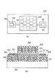
(第1の実施形態)
図1は、本発明の第1の実施形態に係わる発光装置の構造を説明するためのもので、(a)は平面図、(b)は断面図である。
【0028】
図中101はタングステンフィラメントであり、このフィラメント101の両端はそれぞれ金電極102につながっている。金電極102は後述するように、絶縁スペーサ106を介して基板上に固定されている。また、ガラス基板103上に球状のAg(銀)104とTiO2 105からなる3次元フォトニック結晶構造を設けてある。そして、タングステンフィラメント101はSiO2 スペーサ106により空中に保持されている。
【0029】
具体的には、ガラス基板103上に、TiO2 膜105中に球状(直径が数nm〜数十nm)のAg104を規則的に配置してなる3次元の第1のフォトニック結晶構造110が形成され、その上にSiO2 スペーサ106を介して2つの金電極102が所定距離離して取着されている。これらの金電極102間に、タングステンフィラメント101が接続されている。
【0030】
また、第1のフォトニック結晶構造110上の一部には、フィラメント101の両端部を除く領域を覆うように、第1のフォトニック結晶構造110と同様な構成の第2のフォトニック結晶構造120が形成されている。なお、この第2のフォトニック結晶構造120には、フィラメント101と直接接しないようにフィラメント方向に沿って空洞(溝)が設けられている。これによりフィラメント101は、フォトニック結晶構造110,120と直接接することなく、その端部を除いてフォトニック結晶構造110,120で囲まれるものとなっている。
【0031】
このような構成において、フォトニック結晶構造部分の反射率は、図16のように波長1μm以上ではほぼ100%であり、波長0.1μm付近ではほぼ0%であった。そして、タングステンフィラメント101に電流を流して発光スペクトルを測定したところ、フォトニック結晶構造のないものでは、図17の点線で示したように赤外光の放射が主であった。これに対し、本実施形態のようにフォトニック結晶構造を付加したものでは、赤外光の放射が抑えられ、可視光の強度が上がっていた。これは、フォトニック結晶構造によりフィラメント101からの赤外光の放射が抑制されたためであると考えられる。
【0032】
発光効率としては、従来の赤外リフレクター付きのもので50 lm/wであったが、本実施形態では100 lm/wが得られた。
(第2の実施形態)
図2は、本発明の第2の実施形態に係わる発光装置の構造を説明するためのもので、(a)は平面図、(b)は断面図である。なお、図1と同一部分には同一符号を付して、その詳しい説明は省略する。
【0033】
本実施形態が先に説明した第1の実施形態と異なる点は、フォトニック結晶構造の構成にある。即ち、第1の実施形態では球状の金属を誘電体で取り囲んでいたが、本実施形態では2次元的に周期構造を持たせた薄い層を積層してフォトニック結晶構造を構成している。図中201は厚さ約20nmのAg膜、202は厚さ約20nmのTiO2 膜、210は第1のフォトニック結晶構造、220は第2のフォトニック結晶構造である。
【0034】
本実施形態のフォトニック結晶構造を作成するには、例えばガラス基板103上にTiO2 膜202を比較的厚く(20nmよりも厚く)形成した後、このTiO2 膜202の表面に例えば6角形のレジストパターンを配列し、これをマスクにTiO2 膜202をその途中までテーパ状にエッチングする。その後は、下地の形状が反映するような堆積法を用いてAg膜201とTiO2 膜202を順次積層することにより、210のようなフォトニック結晶構造が得られる。
【0035】
本実施形態の構造においても、フォトニック結晶構造により赤外光の放射が抑制されるため、第1の実施形態と同様の効果が得られる。
【0036】
(第3の実施形態)
図3は、本発明の第3の実施形態に係わる発光装置の要部構成を示す鳥瞰図である。
【0037】
図中の301はタングステンフィラメントであり、このフィラメント301と同軸的に筒状のフォトニック結晶構造が配設されている。フォトニック結晶構造は、厚さ約20nmのTiO2 膜302、厚さ約20nmのAg膜303、厚さ約20nmのTiO2 膜302を積層した三層構造となっている。そして、フォトニック結晶構造は支持棒304で支持されている。
【0038】
このような構成でも、フォトニック結晶構造により赤外光の放射が抑制されるため、第1の実施形態とほぼ同様な効果を得ることができる。
【0039】
(第4の実施形態)
図4は、本発明の第4の実施形態に係わる発光装置の構造を説明するためのもので、(a)は平面図、(b)は断面図である。なお、図2と同一部分には同一符号を付して、その詳しい説明は省略する。
【0040】
本実施形態が先に説明した第2の実施形態と異なる点は、フォトニック結晶構造の構成にある。即ち、第2の実施形態ではフォトニック結晶構造を2次元的に形成したが、本実施形態ではフォトニック結晶構造を1次元的に周期構造を持たせて形成している。
【0041】
この場合には、第2の実施形態と同様の効果が得られるのは勿論のこと、熱放射であるにも拘わらず、偏光方向の揃った光を効率良く発生させることが可能である。
【0042】
(第5の実施形態)
図5は、本発明の第5の実施形態に係わる発光装置の構造を説明するためのもので、(a)は平面図、(b)は断面図である。なお、図1と同一部分には同一符号を付して、その詳しい説明は省略する。
【0043】
本実施形態が先に説明した第1の実施形態と異なる点は、フォトニック結晶構造の構成にある。即ち本実施形態では、上側のフォトニック結晶構造120の一部で、球状の金属であるAgを欠落させた、いわゆる欠陥領域501を形成している。
【0044】
この場合には、第1の実施形態と同様の効果が得られるのは勿論のこと、欠陥領域501に光が集中するため、この欠陥領域501から光を効率良く取り出すことができる。即ち、素子の上方に指向性の良い光ビームが得られた。
【0045】
(第6の実施形態)
図6は、本発明の第6の実施形態に係わる発光装置の構造を示す斜視図である。
【0046】
図中の606はSiO2 膜であり、このSiO2 膜606上にSiからなるフィラメント601が橋のように配設されている。即ち、SiO2 膜606の上に所定距離離して2つの電極602が形成され、これらの電極602間にフィラメント601が接続されている。フィラメント601の中央部分が発光領域611であり、この部分を除いてフィラメント601には周期的な孔612が貫通するように設けられている。
【0047】
この場合、フィラメント601に設けた周期的な孔612が1次元のフォトニック結晶構造として機能することになり、フィラメント601からの遠赤外光の光放射は抑制され、効率の良い可視光発光が得られる。
【0048】
(第7の実施形態)
図7は、本発明の第7の実施形態に係わる発光装置の構造を示す断面図である。なお、図6と同一部分には同一符号を付して、その詳しい説明は省略する。
【0049】
本実施形態が先に説明した第6の実施形態と異なる点は、フィラメント601に直交する方向にも、Siフィラメント701及び孔712からなるフォトニック結晶構造を設けた点にある。なお、フィラメント701側に設ける孔712の配列は、光学的欠陥を生じるように発光領域を挟んで位相をずらしてある。
【0050】
本実施形態の構成では、フィラメント701を設けることにより出射ビームの形状が同心円状に近くなり、第6の実施形態よりも更に効率の良い可視光発光が得られた。
【0051】
(第8の実施形態)
図8は、本発明の第8の実施形態に係わる発光装置の構造を示す断面図である。
【0052】
本実施形態はMIS型の発光装置であり、SiC結晶802上に絶縁層804を介して金属電極805が形成され、SiC結晶802の裏面側には所定距離離間して金属電極801がそれぞれ形成されている。そして、2つの金属電極801間のSiC結晶802内には空洞803が規則的に配置され、これによりフォトニック結晶構造が構成されている。
【0053】
本実施形態の構成では、効率の良い青色発光が得られた。
【0054】
(第9の実施形態)
図9は、本発明の第9の実施形態に係わる有機EL発光装置の構造を示す断面図である。
【0055】
図中915は発光層であり、この発光層915は電子輸送層914と正孔輸送層916で挟まれている。上側の電子輸送層914上には透明電極912が形成され、この透明電極912は一部延在して設けられ電極支持台913に固定されている。下側の正孔輸送層916の下面には透明電極911が形成されており、この透明電極911は後述する基板上に形成されている。
【0056】
ガラス基板903上にはSiO2 膜905中に球状のTiO2 904を規則的に配置してなる第1のフォトニック結晶構造が形成され、この上に前記電極911及び電極支持台913が設置されている。また、第1のフォトニック構造上には、EL発光部を覆うように、第1のフォトニック結晶構造と同様の構成の第2のフォトニック構造が形成されている。第2のフォトニック構造において、第5の実施形態と同様に、光学的欠陥を設けるためにTiO2 904の球体を形成していない欠陥領域501が設けられている。
【0057】
本実施形態の構成においては、フォトニック構造の付加により、効率の良い、かつ指向性の強い青色発光が得られた。
【0058】
(第10の実施形態)
図10は、本発明の第10の実施形態に係わる電界放出による蛍光体発光装置の構造を示す断面図である。
【0059】
図中1001は基板であり、この基板1001上にカソード電極1002が形成され、その上にエミッタ1005がアレイ状に配列されている。エミッタ1005間のカソード電極1002上には絶縁層1003が形成され、この絶縁層1003上にゲート電極1004が形成されている。
【0060】
一方、上記のアレイ基板と対向する位置に配置される対向基板は、ガラス基板1009の表面に、蛍光体1007中に球状の空洞1008を規則的に配置してなるフォトニック結晶構造を形成し、その上にアルミ薄膜1006を形成して構成されている。そして、アルミ薄膜1006側がアレイ基板側に対向するようになっている。
【0061】
本実施形態の構成の場合は、空洞によるフォトニックバンド効果で効率の良い蛍光体発光が得られた。
【0062】
(第11の実施形態)
図11は、本発明の第11の実施形態に係わる照明装置の構造を示す平面図である。
【0063】
図中1101は第1の実施形態で示した発光装置であり、基板1100上にアレイ状に並べてある。それぞれの発光装置1101は電気配線1102により並列に接続されている。発光装置1101としては、第2,第4,第5の実施形態のようなものを用いることも勿論可能である。
【0064】
このような構成では、個々の発光装置1101の効率向上により照明装置としても高効率の発光が得られた。
【0065】
(第12の実施形態)
図12は、本発明の第12の実施形態に係わるディスプレイ装置の構成を示す等価回路図である。
【0066】
先の第11の実施形態で示したアレイ状の発光装置の回路構成をこのように変えることで、個々の発光装置の選択的な駆動が可能となり、これにより高効率のディスプレイを実現することができる。なお、1201は発光装置、1202はダイオード、1203は電気配線である。
【0067】
(第13の実施形態)
図13は、本発明の第13の実施形態に係わるディスプレイ装置の動作を説明する模式図である。
【0068】
バックライト付きの液晶ディスプレイでは、発光素子1301からの光は偏光板1302を通って一定の偏光の光のみが液晶パネル1303に到達する。そして、液晶パネル1303で偏光が変化した場合のみ、2つめの偏光板1304を透過し発光点となる。
【0069】
このように、発光素子1301からの光は最初の偏光板1302で半分がカットされるため、通常は複雑な光学系を用いて偏光を揃えることが必要である。これに対し、発光素子1301に第4の実施形態のような発光装置を用いることにより、発光素子1301自体から偏光の揃った光が最初から得られる。従って、偏光を揃えるための複雑な光学系を用いる必要はなく、極めて低コストで高効率のディスプレイ装置が実現可能となる。
【0070】
(第14の実施形態)
図14は、本発明の第14の実施形態に係わるディスプレイ装置の構造を示す平面図である。1401はSi基板であり、このSi基板上にデータ処理用のIC1402、選択駆動が可能な発光素子1404、発光素子1404を駆動するためのIC1403が集積配置されている。
【0071】
この場合の発光素子1404としては、先に説明した各実施形態の発光装置を用いることができる。特に、Siやタングステンをフィラメントとして熱放射を利用する場合には、シリコンLSIとの集積化が容易になり低コストでディスプレイ装置が得られる。
【0072】
(第15の実施形態)
図15は、本発明の第15の実施形態に係わる光電子集積回路の構造を示す平面図である。
【0073】
図中の1501はSi基板、1504は受光素子、1505は発光素子、1506及び1507はシリコンICである。また、1502はフォトニック結晶構造を実現するための空洞、1503は光学的欠陥を形成した領域であり、光の導波路として作用する。
【0074】
このような構成において、IC1506の入力部へ入力があるとその出力部に電圧が発生し、ここに接続された発光素子1505が発光する。発光素子1505からの光は、光導波路1503を通って受け側のIC1507に入力される。このとき、フォトニック結晶構造を利用した導波構造を採用しているので、光導波路1503を急角度に曲げても損失なく導波させることができる。受け側のIC1507では光導波路を通ってきた光を受光素子1504で受光し、これにより出力信号が発生する。
【0075】
本実施形態の構成では、電子素子と光素子を微細に集積化することが容易で、光による配線が可能となる。また、3次元的に集積回路を構成することも可能であり、より複雑な機能を持たせることもできる。
【0076】
なお、本発明は上述した各実施形態に限定されるものではない。熱放射による発光を行うためのフィラメントの材質は、WやSiに限るものではなく、仕様に応じて適宜変更可能である。例えば、SiC,GaN,AlN,炭素,ダイヤモンドを使うこともできる。また、フォトニック結晶構造を実現するための材料も、仕様に応じて適宜変更可能である。
【0077】
その他、本発明の要旨を逸脱しない範囲で、種々変形して実施することができる。
【0078】
【発明の効果】
以上詳述したように本発明によれば、熱放射により光を放射する発光装置において、該熱放射をしている物体に近接した一部にフォトニックバンド構造を有することにより効率良い光の放射を起こすことができる。このため、従来得られなかった高効率の発光装置を実現することができる。その結果、照明装置やディスプレイ装置、或いは光情報処理システムで用いる発光装置やシステムを低コストで得られる。また、シリコンLSIと光素子とを容易に集積することができ、LSIの集積度を上げることも可能である。その信頼性も高く、本発明の有用性は大である。
【図面の簡単な説明】
【図1】第1の実施形態に係わる発光装置の構造を示す平面図及び断面図。
【図2】第2の実施形態に係わる発光装置の構造を示す平面図と断面図。
【図3】第3の実施形態に係わる発光装置の要部を示す鳥瞰図。
【図4】第4の実施形態に係わる発光装置の構造を示す平面図と断面図。
【図5】第5の実施形態に係わる発光装置の構造を示す平面図と断面図。
【図6】第6の実施形態に係わる発光装置の構造を示す鳥瞰図。
【図7】第7の実施形態に係わる発光装置の構造を示す鳥瞰図。
【図8】第8の実施形態に係わる発光装置の構造を示す断面図。
【図9】第9の実施形態に係わる発光装置の構造を示す断面図。
【図10】第10の実施形態に係わる発光装置の構造を示す断面図。
【図11】第11の実施形態に係わる照明装置の構造を示す平面図。
【図12】第12の実施形態に係わるディスプレイ装置の回路を示す図。
【図13】第13の実施形態に係わるディスプレイ装置の動作を説明する図。
【図14】第14の実施形態に係わるディスプレイ装置の構造を示す正面図。
【図15】第15の実施形態に係わる光電子集積回路の模式構造を示す平面図。
【図16】本発明の効果を示すための反射特性を示す図。
【図17】本発明の効果を示すための図。
【図18】従来の照明用電球を説明するための図。
【図19】従来の照明用電球のフィラメント構造を示す平面図と断面図。
【符号の説明】
101,301…タングステンフィラメント
102,602,801,805…電極
103,903,1009…ガラス基板
104…Ag(球状体)
105,202,302…TiO2 膜
106…SiO2 スペーサ
107…空洞(溝)
110,120,210,220…フォトニック結晶構造
201,303…Ag膜
304…支持棒
501…光学的欠陥領域
606,905…SiO2 膜
601,701…Siフィラメント
611…発光領域
612,712…孔
802…SiC結晶
803,1008…球状の空洞
804…絶縁層
904…TiO2 球体
911…透明電極
912…透明電極
913…電極支持台
914…電子輸送層
915…発光層
916…正孔輸送層
1001…アレイ側基板
1002…カソード電極
1003…絶縁層
1004…ゲート
1005…エミッタ
1006…アルミ薄膜
1007…蛍光体[0001]
TECHNICAL FIELD OF THE INVENTION
The present invention relates to a light emitting device used for lighting, display, communication, or the like, a lighting device, a display device, or the like using the same, and an optoelectronic integrated circuit device in which a silicon IC and an optical element are integrated.
[0002]
[Prior art]
Conventionally, various light-emitting devices have been known, but all have low luminous efficiencies, which has been a major problem to be solved. Recently, light sources with low power consumption have been demanded also from the viewpoint of environmental problems, and technical development for improving luminous efficiency has been made. For example, in the case of an incandescent light bulb, most of the heat radiated is infrared light, and very little visible light is the main cause of low efficiency. To improve this, as shown in FIG. A method of attaching an infrared reflective film to a glass bulb of a light bulb has been proposed (Jack Brett et al., 'Radiation-conserving incandescent lamps', J. of IES, p. 197, 1980). In the figure,
[0003]
However, in order to increase the rate at which the reflected infrared light is absorbed by the filament again and to increase the feedback rate, fine adjustment of the filament position or the like is necessary. However, this is limited, and a sufficient effect cannot be obtained.
[0004]
Further, in order to more directly suppress the emission of infrared light from the filament, a method has been proposed in which an array of hollow waveguides is provided on the surface of the light emitter as shown in FIGS. 19 (a) and 19 (b). (US Pat. No. 5,079,473). In the figure,
[0005]
However, even in this case, infrared light is freely radiated from the region between the hollow waveguides. In order to reduce the area of this region and prevent infrared light emission, it is conceivable to make the space between the hollow waveguides narrow, but in this case, the adjacent optical modes are coupled with each other. , The cutoff frequency no longer exists. That is, there has been a problem that infrared light is radiated freely.
[0006]
On the other hand, displays utilizing thermal radiation have also been reported (Frederick Hochberg et al., “A thin-film integrated incandescent display”, IEEE Trans. On Electron Devices, Vol. ED-20, No. ED. 1002, 1973). Although this document reports a display using heat radiation from tungsten, as described above, the ratio of visible light to heat-radiated light is very small, so the luminous efficiency of the light-emitting portion is very low. Unfortunately, the display as a whole has a major problem in terms of efficiency.
[0007]
Further, in optical communication, a laser or an LED is usually used as a light source, but a simpler and lower-cost light source has been desired. Also, in the field of silicon ICs and LSIs, there is no silicon element that emits light efficiently, despite the demand for the realization of optoelectronic integrated circuits. The range was also limited. Further, the increase in the degree of integration of LSIs and the increase in the complexity of multilayered electrical wiring have been one of the biggest obstacles to high integration in the future.
[0008]
[Problems to be solved by the invention]
As described above, conventionally, the efficiency of the light emitting device is generally low, and various measures have been taken to improve the efficiency, but none of the characteristics has been significantly improved. Further, in the LSI, the electric wiring becomes complicated, which hinders high integration.
[0009]
The present invention has been made in view of the above circumstances, and an object of the present invention is to provide a light emitting device having excellent luminous efficiency, and various systems using the same. Another object of the present invention is to provide an optoelectronic integrated circuit device capable of realizing an optical wiring instead of a complicated electric wiring of an LSI.
[0010]
[Means for Solving the Problems]
(Constitution)
In order to solve the above problems, the present invention employs the following configuration.
[0011]
That is, the present invention includes a filament that emits light by light emission by thermal radiation, a light-emitting device comprising; and a photonic crystal structure in a non-contact disposed proximate to the filament and the filament, the photonic The crystal structure suppresses the emission of light in the infrared light region from the filament and enhances the emission of light in the visible light region .
[0013]
Further, the invention is characterized in that the light-emitting devices having the above-described configuration are arranged in an array to constitute a lighting device or a display device.
[0014]
Further, the present invention is characterized in that the light emitting device having the above structure is integrated with a silicon IC to constitute an optoelectronic integrated circuit device.
[0015]
Here, preferred embodiments of the present invention include the following.
[0016]
(1) A photonic crystal structure in which metal spherical bodies are regularly arranged in a dielectric film. In addition, a defect region in which a metal spherical body is missing is provided in a part of the dielectric film.
[0017]
(2) As a photonic crystal structure, spherical bodies or cavities of a second dielectric material having a different refractive index from the first dielectric film are regularly arranged. Further, a defect region in which a part of a spherical body or a cavity of the second dielectric is missing is provided in a part of the first dielectric film.
[0018]
(3) A laminated structure of a dielectric film and a metal film is formed as a photonic crystal structure. Further, the laminated structure of the dielectric film and the metal film has a one-dimensional or two-dimensional periodic structure.
[0019]
(Action)
In the present invention, by providing a photonic crystal structure in at least a part close to the light emitting portion that emits light, at least a part of the emission of light other than the desired wavelength band is suppressed, or the desired wavelength band is suppressed. It is characterized in that at least a part of light is enhanced. For example, visible light can be set as a desired wavelength band, and emission of infrared light can be suppressed.
[0020]
The emission spectrum of conventional thermal radiation is expressed as the blackbody radiation spectrum determined by Planck's equation multiplied by the emissivity specific to the radiator material. When the temperature of the light emitting section is about 2000 ° C., the ratio of visible light in the spectrum is very small. The photonic crystal structure referred to here means that an optical band is formed by arranging one or more pairs of two or more kinds of media periodically or with a shift in the period to give light anisotropy or dispersibility. Is an artificial crystal in which light of a specific wavelength range cannot be propagated. The crystal structure can be one-dimensional to three-dimensional.
[0021]
The concept of a photonic bandgap has been proposed in the literature (E. Yablonovitch, Phys. Rev. Lett., 58, p2059, 1987). By arranging this photonic crystal close to the light emitting unit, light in a specific wavelength range cannot be emitted from the light emitting unit. For example, if the optical band gap is set in the infrared region, the emission of infrared light can be suppressed, and the ratio of visible light can be increased.
[0022]
Further, according to the present invention, a photonic crystal structure is provided in at least a part close to a light emitting portion that emits light to control the polarization state of light in a desired wavelength band or to adjust the radiation pattern of light in a desired wavelength band. Is controlled. In this case, it is possible to increase the light that can be actually used among the radiated light in the desired wavelength band, and to substantially increase the luminous efficiency.
[0023]
The above is the case where the present invention is applied to visible light, but it is similarly possible to set so that near-infrared light used in optical communication, particularly light near 1300 nm or 1550 nm can be efficiently emitted.
[0024]
Further, the present invention is characterized in that the photonic band structure contains at least a metal. In this case, the optical band gap can be particularly increased, and the emission spectrum can be controlled over a wide wavelength range from visible light to far infrared. For this reason, a light source with higher efficiency becomes possible. Further, in the present invention, by arranging these high-efficiency light-emitting devices in an array, it is possible to realize a lighting device and a display device having high luminance as well as high efficiency. In particular, when a light source whose polarization is controlled is used as a backlight of a liquid crystal display device, a significant improvement in efficiency can be achieved because a polarization component which has been wasted in the past is not originally present.
[0025]
Further, in the present invention, by forming the luminous body region that emits heat radiation from, for example, silicon or tungsten, the silicon LSI and the optical element can be easily integrated. Further, in the present invention, a light emitting element utilizing heat radiation formed on an LSI and an optical waveguide utilizing a photonic crystal structure are combined to replace at least a part of the conventional electric wiring with an optical wiring, thereby simplifying the wiring. And it is easy to increase the degree of integration of the LSI.
[0026]
BEST MODE FOR CARRYING OUT THE INVENTION
Hereinafter, the present invention will be described in detail with reference to the illustrated embodiments.
[0027]
(1st Embodiment)
1A and 1B are views for explaining the structure of a light emitting device according to a first embodiment of the present invention, wherein FIG. 1A is a plan view and FIG. 1B is a cross-sectional view.
[0028]
In the figure,
[0029]
Specifically, on a
[0030]
In addition, a second photonic crystal structure having the same configuration as the first
[0031]
In such a configuration, the reflectivity of the photonic crystal structure portion was almost 100% at a wavelength of 1 μm or more and almost 0% near a wavelength of 0.1 μm as shown in FIG. Then, when a current was applied to the
[0032]
The luminous efficiency was 50 lm / w with the conventional infrared reflector, but in the present embodiment, 100 lm / w was obtained.
(Second embodiment)
2A and 2B are views for explaining the structure of a light emitting device according to a second embodiment of the present invention, wherein FIG. 2A is a plan view and FIG. 2B is a cross-sectional view. The same parts as those in FIG. 1 are denoted by the same reference numerals, and detailed description thereof will be omitted.
[0033]
This embodiment differs from the first embodiment described above in the configuration of the photonic crystal structure. That is, in the first embodiment, the spherical metal is surrounded by the dielectric, but in the present embodiment, a thin layer having a two-dimensional periodic structure is stacked to form a photonic crystal structure. In the figure, 201 is an Ag film having a thickness of about 20 nm, 202 is a TiO 2 film having a thickness of about 20 nm, 210 is a first photonic crystal structure, and 220 is a second photonic crystal structure.
[0034]
In order to form the photonic crystal structure of the present embodiment, for example, after forming the TiO 2 film 202 on the
[0035]
Also in the structure of the present embodiment, the radiation of infrared light is suppressed by the photonic crystal structure, so that the same effect as in the first embodiment can be obtained.
[0036]
(Third embodiment)
FIG. 3 is a bird's-eye view showing a configuration of a main part of a light emitting device according to a third embodiment of the present invention.
[0037]
In the figure, reference numeral 301 denotes a tungsten filament, and a cylindrical photonic crystal structure is arranged coaxially with the filament 301. The photonic crystal structure has a three-layer structure in which a TiO 2 film 302 having a thickness of about 20 nm, an Ag film 303 having a thickness of about 20 nm, and a TiO 2 film 302 having a thickness of about 20 nm are stacked. The photonic crystal structure is supported by the support rod 304.
[0038]
Even in such a configuration, since the emission of infrared light is suppressed by the photonic crystal structure, substantially the same effect as in the first embodiment can be obtained.
[0039]
(Fourth embodiment)
4A and 4B are diagrams for explaining the structure of a light emitting device according to a fourth embodiment of the present invention, wherein FIG. 4A is a plan view and FIG. 4B is a cross-sectional view. The same parts as those in FIG. 2 are denoted by the same reference numerals, and detailed description thereof will be omitted.
[0040]
This embodiment differs from the second embodiment described above in the configuration of the photonic crystal structure. That is, in the second embodiment, the photonic crystal structure is formed two-dimensionally, but in the present embodiment, the photonic crystal structure is formed to have a one-dimensional periodic structure.
[0041]
In this case, not only the same effects as in the second embodiment can be obtained, but also light having a uniform polarization direction can be efficiently generated in spite of heat radiation.
[0042]
(Fifth embodiment)
5A and 5B are views for explaining the structure of a light emitting device according to a fifth embodiment of the present invention, wherein FIG. 5A is a plan view and FIG. 5B is a cross-sectional view. The same parts as those in FIG. 1 are denoted by the same reference numerals, and detailed description thereof will be omitted.
[0043]
This embodiment differs from the first embodiment described above in the configuration of the photonic crystal structure. That is, in the present embodiment, a so-called
[0044]
In this case, the same effects as those of the first embodiment can be obtained, and the light can be efficiently extracted from the
[0045]
(Sixth embodiment)
FIG. 6 is a perspective view illustrating a structure of a light emitting device according to a sixth embodiment of the present invention.
[0046]
606 in the figure is a SiO 2 film,
[0047]
In this case, the
[0048]
(Seventh embodiment)
FIG. 7 is a cross-sectional view illustrating a structure of a light emitting device according to a seventh embodiment of the present invention. The same parts as those in FIG. 6 are denoted by the same reference numerals, and detailed description thereof will be omitted.
[0049]
This embodiment is different from the above-described sixth embodiment in that a photonic crystal structure including a
[0050]
In the configuration of the present embodiment, the provision of the
[0051]
(Eighth embodiment)
FIG. 8 is a sectional view showing a structure of a light emitting device according to the eighth embodiment of the present invention.
[0052]
This embodiment is a MIS type light emitting device, in which a
[0053]
In the configuration of the present embodiment, efficient blue light emission was obtained.
[0054]
(Ninth embodiment)
FIG. 9 is a sectional view showing a structure of an organic EL light emitting device according to a ninth embodiment of the present invention.
[0055]
In the figure,
[0056]
A first photonic crystal structure in which
[0057]
In the configuration of this embodiment, efficient and strong directivity blue light emission was obtained by the addition of the photonic structure.
[0058]
(Tenth embodiment)
FIG. 10 is a sectional view showing a structure of a phosphor light emitting device using field emission according to a tenth embodiment of the present invention.
[0059]
In the figure,
[0060]
On the other hand, an opposing substrate arranged at a position opposing the above-mentioned array substrate forms a photonic crystal structure in which
[0061]
In the case of the configuration of the present embodiment, efficient phosphor emission was obtained by the photonic band effect due to the cavity.
[0062]
(Eleventh embodiment)
FIG. 11 is a plan view showing a structure of a lighting device according to an eleventh embodiment of the present invention.
[0063]
In the figure,
[0064]
In such a configuration, high efficiency light emission was obtained also as a lighting device by improving the efficiency of each light emitting
[0065]
(Twelfth embodiment)
FIG. 12 is an equivalent circuit diagram showing a configuration of a display device according to the twelfth embodiment of the present invention.
[0066]
By changing the circuit configuration of the array-like light-emitting device described in the eleventh embodiment in this way, it is possible to selectively drive individual light-emitting devices, thereby realizing a highly efficient display. it can. Note that 1201 is a light emitting device, 1202 is a diode, and 1203 is an electric wiring.
[0067]
(Thirteenth embodiment)
FIG. 13 is a schematic diagram illustrating the operation of the display device according to the thirteenth embodiment of the present invention.
[0068]
In a liquid crystal display with a backlight, light from the
[0069]
As described above, since half of the light from the
[0070]
(14th embodiment)
FIG. 14 is a plan view illustrating a structure of a display device according to a fourteenth embodiment of the present invention. Reference numeral 1401 denotes a Si substrate on which an
[0071]
In this case, as the
[0072]
(Fifteenth embodiment)
FIG. 15 is a plan view showing the structure of the optoelectronic integrated circuit according to the fifteenth embodiment of the present invention.
[0073]
In the figure, 1501 is a Si substrate, 1504 is a light receiving element, 1505 is a light emitting element, and 1506 and 1507 are silicon ICs.
[0074]
In such a configuration, when an input is made to the input portion of the
[0075]
In the configuration of the present embodiment, it is easy to finely integrate the electronic element and the optical element, and wiring by light is possible. Further, an integrated circuit can be formed three-dimensionally, and more complicated functions can be provided.
[0076]
Note that the present invention is not limited to the above embodiments. The material of the filament for emitting light by thermal radiation is not limited to W or Si, and can be appropriately changed according to specifications. For example, SiC, GaN, AlN, carbon, and diamond can be used. Further, the material for realizing the photonic crystal structure can be appropriately changed according to the specifications.
[0077]
In addition, various modifications can be made without departing from the scope of the present invention.
[0078]
【The invention's effect】
As described above in detail, according to the present invention, in a light emitting device that emits light by heat radiation, efficient light emission is achieved by having a photonic band structure in a part close to the object that is emitting the heat. Can be caused. Therefore, a highly efficient light emitting device that has not been obtained conventionally can be realized. As a result, a lighting device, a display device, or a light emitting device or system used in an optical information processing system can be obtained at low cost. Further, the silicon LSI and the optical element can be easily integrated, and the integration degree of the LSI can be increased. The reliability is high, and the usefulness of the present invention is great.
[Brief description of the drawings]
FIG. 1 is a plan view and a cross-sectional view illustrating a structure of a light emitting device according to a first embodiment.
FIGS. 2A and 2B are a plan view and a cross-sectional view illustrating a structure of a light emitting device according to a second embodiment.
FIG. 3 is a bird's-eye view showing a main part of a light emitting device according to a third embodiment.
FIG. 4 is a plan view and a cross-sectional view illustrating a structure of a light emitting device according to a fourth embodiment.
FIGS. 5A and 5B are a plan view and a cross-sectional view illustrating a structure of a light emitting device according to a fifth embodiment.
FIG. 6 is a bird's-eye view showing a structure of a light emitting device according to a sixth embodiment.
FIG. 7 is a bird's-eye view showing a structure of a light emitting device according to a seventh embodiment.
FIG. 8 is a sectional view showing the structure of a light emitting device according to an eighth embodiment.
FIG. 9 is a sectional view showing the structure of a light emitting device according to a ninth embodiment.
FIG. 10 is a sectional view showing a structure of a light emitting device according to a tenth embodiment.
FIG. 11 is a plan view showing the structure of a lighting device according to an eleventh embodiment.
FIG. 12 is a diagram showing a circuit of a display device according to a twelfth embodiment.
FIG. 13 is a view for explaining the operation of the display device according to the thirteenth embodiment.
FIG. 14 is an exemplary front view showing the structure of a display device according to a fourteenth embodiment;
FIG. 15 is a plan view showing a schematic structure of an optoelectronic integrated circuit according to a fifteenth embodiment.
FIG. 16 is a diagram showing reflection characteristics for showing the effect of the present invention.
FIG. 17 is a diagram showing the effect of the present invention.
FIG. 18 is a view for explaining a conventional lighting bulb.
FIG. 19 is a plan view and a cross-sectional view showing a filament structure of a conventional lighting bulb.
[Explanation of symbols]
101, 301:
105, 202, 302: TiO 2 film 106: SiO 2 spacer 107: cavity (groove)
110, 120, 210 ... photonic crystal structure 201,303 ... Ag film 304 ... supporting
Claims (5)
前記フォトニック結晶構造により前記フィラメントにおける赤外光領域の光の放射を抑制し、且つ可視光領域の光の放射を増強させることを特徴とする発光装置。A filament that emits light by emission of heat radiation , and the filament includes a photonic crystal structure disposed in close contact with the filament in a non-contact manner,
A light-emitting device, wherein the photonic crystal structure suppresses emission of light in an infrared light region from the filament and enhances emission of light in a visible light region .
Priority Applications (2)
| Application Number | Priority Date | Filing Date | Title |
|---|---|---|---|
| JP7507099A JP3576859B2 (en) | 1999-03-19 | 1999-03-19 | Light emitting device and system using the same |
| US09/531,490 US6586775B2 (en) | 1999-03-19 | 2000-03-20 | Light-emitting device and a display apparatus having a light-emitting device |
Applications Claiming Priority (1)
| Application Number | Priority Date | Filing Date | Title |
|---|---|---|---|
| JP7507099A JP3576859B2 (en) | 1999-03-19 | 1999-03-19 | Light emitting device and system using the same |
Publications (2)
| Publication Number | Publication Date |
|---|---|
| JP2000267585A JP2000267585A (en) | 2000-09-29 |
| JP3576859B2 true JP3576859B2 (en) | 2004-10-13 |
Family
ID=13565579
Family Applications (1)
| Application Number | Title | Priority Date | Filing Date |
|---|---|---|---|
| JP7507099A Expired - Fee Related JP3576859B2 (en) | 1999-03-19 | 1999-03-19 | Light emitting device and system using the same |
Country Status (2)
| Country | Link |
|---|---|
| US (1) | US6586775B2 (en) |
| JP (1) | JP3576859B2 (en) |
Families Citing this family (45)
| Publication number | Priority date | Publication date | Assignee | Title |
|---|---|---|---|---|
| US7075610B2 (en) * | 1997-09-16 | 2006-07-11 | Michael Scalora | Liquid crystal display device and light emitting structure with photonic band gap transparent electrode structures |
| US5876621A (en) * | 1997-09-30 | 1999-03-02 | Sapienza; Richard | Environmentally benign anti-icing or deicing fluids |
| JP2001196162A (en) * | 1999-10-25 | 2001-07-19 | Seiko Epson Corp | Light emitting device |
| NO20014399L (en) * | 2000-11-29 | 2002-05-30 | Hewlett Packard Co | A data structure and storage and retrieval method that supports ordinal number based data retrieval and retrieval |
| ITTO20010341A1 (en) * | 2001-04-10 | 2002-10-10 | Fiat Ricerche | MICROFILAMENT MATRIX LIGHT SOURCE. |
| US6936854B2 (en) | 2001-05-10 | 2005-08-30 | Canon Kabushiki Kaisha | Optoelectronic substrate |
| US6768256B1 (en) | 2001-08-27 | 2004-07-27 | Sandia Corporation | Photonic crystal light source |
| US6611085B1 (en) | 2001-08-27 | 2003-08-26 | Sandia Corporation | Photonically engineered incandescent emitter |
| ITTO20020031A1 (en) * | 2002-01-11 | 2003-07-11 | Fiat Ricerche | THREE-DIMENSIONAL TUNGSTEN STRUCTURE FOR AN INCANDESCENT LAMP AND LIGHT SOURCE INCLUDING SUCH STRUCTURE. |
| US6979105B2 (en) * | 2002-01-18 | 2005-12-27 | Leysath Joseph A | Light device with photonic band pass filter |
| GB0216931D0 (en) * | 2002-07-20 | 2002-08-28 | Bae Systems Plc | Incandescent lighting |
| ITTO20030167A1 (en) | 2003-03-06 | 2004-09-07 | Fiat Ricerche | PROCEDURE FOR THE CREATION OF NANO-STRUCTURED EMITTERS FOR INCANDESCENT LIGHT SOURCES. |
| DE10318480A1 (en) * | 2003-04-23 | 2004-11-18 | Itn Nanovation Gmbh | Photonic crystal |
| US6940174B2 (en) * | 2003-12-23 | 2005-09-06 | National Taiwan University | Metallic photonic box and its fabrication techniques |
| KR100639683B1 (en) * | 2004-01-07 | 2006-10-27 | 학교법인 조선대학교 | LED using Photonic crystal structure and method of fabricating the same |
| JP4231418B2 (en) * | 2004-01-07 | 2009-02-25 | 株式会社小糸製作所 | Light emitting module and vehicle lamp |
| ITTO20040018A1 (en) * | 2004-01-16 | 2004-04-16 | Fiat Ricerche | LIGHT-EMITTING DEVICE |
| US7368870B2 (en) * | 2004-10-06 | 2008-05-06 | Hewlett-Packard Development Company, L.P. | Radiation emitting structures including photonic crystals |
| US20060124952A1 (en) * | 2004-12-10 | 2006-06-15 | Milligan Donald J | Light emitter |
| WO2006086117A2 (en) * | 2005-01-13 | 2006-08-17 | Massachusetts Institute Of Technology | Vertical-cavity enhanced resonant thermal emitter |
| US7394587B2 (en) * | 2005-01-28 | 2008-07-01 | Hewlett-Packard Development Company, L.P. | Apparatus having a photonic crystal |
| DE102005008077B4 (en) * | 2005-02-22 | 2007-01-18 | Fraunhofer-Gesellschaft zur Förderung der angewandten Forschung e.V. | Radiator, and device and method for analyzing the qualitative and / or quantitative composition of fluids with such a radiator |
| US7722421B2 (en) * | 2006-03-31 | 2010-05-25 | General Electric Company | High temperature ceramic composite for selective emission |
| US8044567B2 (en) | 2006-03-31 | 2011-10-25 | General Electric Company | Light source incorporating a high temperature ceramic composite and gas phase for selective emission |
| US7851985B2 (en) | 2006-03-31 | 2010-12-14 | General Electric Company | Article incorporating a high temperature ceramic composite for selective emission |
| US20070228986A1 (en) * | 2006-03-31 | 2007-10-04 | General Electric Company | Light source incorporating a high temperature ceramic composite for selective emission |
| WO2007139022A1 (en) * | 2006-05-26 | 2007-12-06 | Nalux Co., Ltd. | Infrared light source and its fabrication method |
| WO2007141826A1 (en) | 2006-05-26 | 2007-12-13 | Nalux Co., Ltd. | Infrared light source |
| US20080231184A1 (en) * | 2006-06-19 | 2008-09-25 | Iowa State University Research Foundation, Inc. | Higher efficiency incandescent lighting using photon recycling |
| US7625515B2 (en) * | 2006-06-19 | 2009-12-01 | Iowa State University Research Foundation, Inc. | Fabrication of layer-by-layer photonic crystals using two polymer microtransfer molding |
| US7808005B1 (en) * | 2007-04-26 | 2010-10-05 | Hewlett-Packard Development Company, L.P. | Light-emitting device with photonic grating configured for extracting light from light-emitting structure |
| US20090085463A1 (en) * | 2007-09-28 | 2009-04-02 | General Electric Company | Thermo-optically functional compositions, systems and methods of making |
| DE102007060839A1 (en) * | 2007-12-18 | 2009-06-25 | Osram Gesellschaft mit beschränkter Haftung | Illuminant and lamp with a one-dimensional photonic crystal |
| US20090160314A1 (en) * | 2007-12-20 | 2009-06-25 | General Electric Company | Emissive structures and systems |
| KR101478339B1 (en) * | 2008-06-19 | 2015-01-08 | 서울바이오시스 주식회사 | Light emitting device and method of manufacturing |
| US8138675B2 (en) * | 2009-02-27 | 2012-03-20 | General Electric Company | Stabilized emissive structures and methods of making |
| US9400219B2 (en) * | 2009-05-19 | 2016-07-26 | Iowa State University Research Foundation, Inc. | Metallic layer-by-layer photonic crystals for linearly-polarized thermal emission and thermophotovoltaic device including same |
| US20120286643A1 (en) * | 2009-11-12 | 2012-11-15 | Opalux Incorporated | Photonic Crystal Incandescent Light Source |
| US8742406B1 (en) | 2011-02-16 | 2014-06-03 | Iowa State University Research Foundation, Inc. | Soft lithography microlens fabrication and array for enhanced light extraction from organic light emitting diodes (OLEDs) |
| WO2014080478A1 (en) * | 2012-11-21 | 2014-05-30 | パイオニア株式会社 | Light emitting device and method for producing light emitting device |
| WO2014080477A1 (en) * | 2012-11-21 | 2014-05-30 | パイオニア株式会社 | Light emitting device |
| GB2554236A (en) * | 2015-06-04 | 2018-03-28 | Halliburton Energy Services Inc | Methods and systems using photonic crystal-based integrated computational elements |
| JP6762533B2 (en) * | 2016-09-09 | 2020-09-30 | 大阪瓦斯株式会社 | Thermal radiation light source and light source device |
| US11061499B2 (en) * | 2018-12-12 | 2021-07-13 | Wuhan China Star Optoelectronics Semiconductor Display Technology Co., Ltd. | Display panel |
| KR102892171B1 (en) * | 2019-02-18 | 2025-11-28 | 삼성디스플레이 주식회사 | Display device |
Family Cites Families (16)
| Publication number | Priority date | Publication date | Assignee | Title |
|---|---|---|---|---|
| US4689519A (en) * | 1985-10-23 | 1987-08-25 | U.S. Philips Corporation | Electric lamp having an outwardly extending protrusion |
| US5079473A (en) | 1989-09-08 | 1992-01-07 | John F. Waymouth Intellectual Property And Education Trust | Optical light source device |
| US5385114A (en) * | 1992-12-04 | 1995-01-31 | Milstein; Joseph B. | Photonic band gap materials and method of preparation thereof |
| DE69407312T2 (en) * | 1993-01-07 | 1998-07-23 | Nippon Electric Co | Integrated semiconductor optical device and manufacturing method |
| US5440421A (en) * | 1994-05-10 | 1995-08-08 | Massachusetts Institute Of Technology | Three-dimensional periodic dielectric structures having photonic bandgaps |
| US6011580A (en) * | 1994-06-07 | 2000-01-04 | Terumo Kabushiki Kaisha | Image display apparatus |
| US5784400A (en) | 1995-02-28 | 1998-07-21 | Massachusetts Institute Of Technology | Resonant cavities employing two dimensionally periodic dielectric materials |
| WO1996029621A1 (en) * | 1995-03-17 | 1996-09-26 | Massachusetts Institute Of Technology | Metallodielectric photonic crystal |
| DE19526734A1 (en) * | 1995-07-21 | 1997-01-23 | Siemens Ag | Optical structure and process for its manufacture |
| GB9607862D0 (en) * | 1996-04-16 | 1996-06-19 | Smiths Industries Plc | Light-emitting assemblies |
| WO1998026316A1 (en) * | 1996-12-13 | 1998-06-18 | Massachusetts Institute Of Technology | Tunable microcavity using nonlinear materials in a photonic crystal |
| FR2765712B1 (en) * | 1997-07-04 | 1999-09-17 | Soc D Expl Du Mobilier A Usage | LIGHT DISPLAY PANEL |
| JP3542504B2 (en) * | 1997-08-28 | 2004-07-14 | キヤノン株式会社 | Color display |
| US6262830B1 (en) * | 1997-09-16 | 2001-07-17 | Michael Scalora | Transparent metallo-dielectric photonic band gap structure |
| US5999308A (en) * | 1998-04-01 | 1999-12-07 | Massachusetts Institute Of Technology | Methods and systems for introducing electromagnetic radiation into photonic crystals |
| US5998298A (en) * | 1998-04-28 | 1999-12-07 | Sandia Corporation | Use of chemical-mechanical polishing for fabricating photonic bandgap structures |
-
1999
- 1999-03-19 JP JP7507099A patent/JP3576859B2/en not_active Expired - Fee Related
-
2000
- 2000-03-20 US US09/531,490 patent/US6586775B2/en not_active Expired - Fee Related
Also Published As
| Publication number | Publication date |
|---|---|
| US20030071564A1 (en) | 2003-04-17 |
| US6586775B2 (en) | 2003-07-01 |
| JP2000267585A (en) | 2000-09-29 |
Similar Documents
| Publication | Publication Date | Title |
|---|---|---|
| JP3576859B2 (en) | Light emitting device and system using the same | |
| KR102139291B1 (en) | Illumination device | |
| JP6063394B2 (en) | Lighting device | |
| CN103456869B (en) | Light-emitting device, light-emitting diode chip and sapphire substrate for forming multi-directional light output | |
| US7335921B2 (en) | Lighting devices using feedback enhanced light emitting diode | |
| TWI681554B (en) | Pixel array substrate and driving method thereof | |
| JP2002319705A (en) | LED device | |
| WO2017186024A1 (en) | Led display module, display device and manufacturing method of display module | |
| US8885122B2 (en) | Light emitting diode, method of fabricating the same, and liquid crystal display including the same | |
| US20120068214A1 (en) | Optoelectronic device and method for manufacturing the same | |
| US20130334555A1 (en) | Optoelectronic device and method for manufacturing the same | |
| JP2016012707A (en) | Photoelectric component and manufacturing method of the same | |
| JP2005340625A5 (en) | ||
| TWI766900B (en) | Light emitting device | |
| KR102052040B1 (en) | Optoelectronic device and method for manufacturing the same | |
| US20140264390A1 (en) | Optoelectronic device and method for manufacturing the same | |
| TWI787987B (en) | Optoelectronic device | |
| KR102907491B1 (en) | Light source and image projection device | |
| CN100399567C (en) | flat display panel | |
| CN108269902A (en) | A kind of LED encapsulation structure and its packaging method | |
| US20140167097A1 (en) | Optoelectronic device and method for manufacturing the same | |
| TWI603498B (en) | Side view light-emitting laser element | |
| US9236947B2 (en) | Fast thin-film light emitting diode | |
| KR20190137038A (en) | Optoelectronic device | |
| TW202431665A (en) | Optoelectronic device |
Legal Events
| Date | Code | Title | Description |
|---|---|---|---|
| A131 | Notification of reasons for refusal |
Free format text: JAPANESE INTERMEDIATE CODE: A131 Effective date: 20040224 |
|
| A521 | Request for written amendment filed |
Free format text: JAPANESE INTERMEDIATE CODE: A523 Effective date: 20040426 |
|
| TRDD | Decision of grant or rejection written | ||
| A01 | Written decision to grant a patent or to grant a registration (utility model) |
Free format text: JAPANESE INTERMEDIATE CODE: A01 Effective date: 20040706 |
|
| A61 | First payment of annual fees (during grant procedure) |
Free format text: JAPANESE INTERMEDIATE CODE: A61 Effective date: 20040708 |
|
| FPAY | Renewal fee payment (event date is renewal date of database) |
Free format text: PAYMENT UNTIL: 20080716 Year of fee payment: 4 |
|
| FPAY | Renewal fee payment (event date is renewal date of database) |
Free format text: PAYMENT UNTIL: 20090716 Year of fee payment: 5 |
|
| FPAY | Renewal fee payment (event date is renewal date of database) |
Free format text: PAYMENT UNTIL: 20090716 Year of fee payment: 5 |
|
| FPAY | Renewal fee payment (event date is renewal date of database) |
Free format text: PAYMENT UNTIL: 20100716 Year of fee payment: 6 |
|
| FPAY | Renewal fee payment (event date is renewal date of database) |
Free format text: PAYMENT UNTIL: 20110716 Year of fee payment: 7 |
|
| FPAY | Renewal fee payment (event date is renewal date of database) |
Free format text: PAYMENT UNTIL: 20120716 Year of fee payment: 8 |
|
| FPAY | Renewal fee payment (event date is renewal date of database) |
Free format text: PAYMENT UNTIL: 20130716 Year of fee payment: 9 |
|
| LAPS | Cancellation because of no payment of annual fees |