JP3564104B2 - Exposure apparatus, control method therefor, and device manufacturing method using the same - Google Patents
Exposure apparatus, control method therefor, and device manufacturing method using the same Download PDFInfo
- Publication number
- JP3564104B2 JP3564104B2 JP2002020213A JP2002020213A JP3564104B2 JP 3564104 B2 JP3564104 B2 JP 3564104B2 JP 2002020213 A JP2002020213 A JP 2002020213A JP 2002020213 A JP2002020213 A JP 2002020213A JP 3564104 B2 JP3564104 B2 JP 3564104B2
- Authority
- JP
- Japan
- Prior art keywords
- light
- exposure
- reticle
- reflection
- exposure apparatus
- Prior art date
- Legal status (The legal status is an assumption and is not a legal conclusion. Google has not performed a legal analysis and makes no representation as to the accuracy of the status listed.)
- Expired - Fee Related
Links
Images


Classifications
-
- G—PHYSICS
- G03—PHOTOGRAPHY; CINEMATOGRAPHY; ANALOGOUS TECHNIQUES USING WAVES OTHER THAN OPTICAL WAVES; ELECTROGRAPHY; HOLOGRAPHY
- G03F—PHOTOMECHANICAL PRODUCTION OF TEXTURED OR PATTERNED SURFACES, e.g. FOR PRINTING, FOR PROCESSING OF SEMICONDUCTOR DEVICES; MATERIALS THEREFOR; ORIGINALS THEREFOR; APPARATUS SPECIALLY ADAPTED THEREFOR
- G03F7/00—Photomechanical, e.g. photolithographic, production of textured or patterned surfaces, e.g. printing surfaces; Materials therefor, e.g. comprising photoresists; Apparatus specially adapted therefor
- G03F7/70—Microphotolithographic exposure; Apparatus therefor
- G03F7/70483—Information management; Active and passive control; Testing; Wafer monitoring, e.g. pattern monitoring
- G03F7/7055—Exposure light control in all parts of the microlithographic apparatus, e.g. pulse length control or light interruption
- G03F7/70558—Dose control, i.e. achievement of a desired dose
-
- G—PHYSICS
- G03—PHOTOGRAPHY; CINEMATOGRAPHY; ANALOGOUS TECHNIQUES USING WAVES OTHER THAN OPTICAL WAVES; ELECTROGRAPHY; HOLOGRAPHY
- G03F—PHOTOMECHANICAL PRODUCTION OF TEXTURED OR PATTERNED SURFACES, e.g. FOR PRINTING, FOR PROCESSING OF SEMICONDUCTOR DEVICES; MATERIALS THEREFOR; ORIGINALS THEREFOR; APPARATUS SPECIALLY ADAPTED THEREFOR
- G03F7/00—Photomechanical, e.g. photolithographic, production of textured or patterned surfaces, e.g. printing surfaces; Materials therefor, e.g. comprising photoresists; Apparatus specially adapted therefor
- G03F7/70—Microphotolithographic exposure; Apparatus therefor
- G03F7/70058—Mask illumination systems
- G03F7/70075—Homogenization of illumination intensity in the mask plane by using an integrator, e.g. fly's eye lens, facet mirror or glass rod, by using a diffusing optical element or by beam deflection
-
- G—PHYSICS
- G03—PHOTOGRAPHY; CINEMATOGRAPHY; ANALOGOUS TECHNIQUES USING WAVES OTHER THAN OPTICAL WAVES; ELECTROGRAPHY; HOLOGRAPHY
- G03F—PHOTOMECHANICAL PRODUCTION OF TEXTURED OR PATTERNED SURFACES, e.g. FOR PRINTING, FOR PROCESSING OF SEMICONDUCTOR DEVICES; MATERIALS THEREFOR; ORIGINALS THEREFOR; APPARATUS SPECIALLY ADAPTED THEREFOR
- G03F7/00—Photomechanical, e.g. photolithographic, production of textured or patterned surfaces, e.g. printing surfaces; Materials therefor, e.g. comprising photoresists; Apparatus specially adapted therefor
- G03F7/70—Microphotolithographic exposure; Apparatus therefor
- G03F7/70058—Mask illumination systems
- G03F7/702—Reflective illumination, i.e. reflective optical elements other than folding mirrors, e.g. extreme ultraviolet [EUV] illumination systems
-
- G—PHYSICS
- G03—PHOTOGRAPHY; CINEMATOGRAPHY; ANALOGOUS TECHNIQUES USING WAVES OTHER THAN OPTICAL WAVES; ELECTROGRAPHY; HOLOGRAPHY
- G03F—PHOTOMECHANICAL PRODUCTION OF TEXTURED OR PATTERNED SURFACES, e.g. FOR PRINTING, FOR PROCESSING OF SEMICONDUCTOR DEVICES; MATERIALS THEREFOR; ORIGINALS THEREFOR; APPARATUS SPECIALLY ADAPTED THEREFOR
- G03F7/00—Photomechanical, e.g. photolithographic, production of textured or patterned surfaces, e.g. printing surfaces; Materials therefor, e.g. comprising photoresists; Apparatus specially adapted therefor
- G03F7/70—Microphotolithographic exposure; Apparatus therefor
- G03F7/70216—Mask projection systems
- G03F7/70233—Optical aspects of catoptric systems, i.e. comprising only reflective elements, e.g. extreme ultraviolet [EUV] projection systems
Landscapes
- Physics & Mathematics (AREA)
- General Physics & Mathematics (AREA)
- Exposure Of Semiconductors, Excluding Electron Or Ion Beam Exposure (AREA)
- Exposure And Positioning Against Photoresist Photosensitive Materials (AREA)
Description
【0001】
【発明の属する技術分野】
本発明は微細な回路パターンを転写可能な露光装置およびその制御方法に関する。
【0002】
【従来の技術】
従来、半導体メモリや論理回路などの微細な半導体素子を製造するための焼き付け(リソグラフィー)方法として、紫外線を用いた縮小投影露光が行われてきた。
【0003】
縮小投影露光で転写できる最小の寸法は転写に用いる光の波長に比例し、投影光学系の開口数に反比例する。このため、微細な回路パターンを転写するためには、用いる光の短波長化を進めることが必要となる。このため、水銀ランプi線(波長365nm)、KrFエキシマレーザ(波長248nm)、ArFエキシマレーザ(波長193nm)というように用いられる紫外光の波長は短くなってきている。
【0004】
しかし半導体素子は急速に微細化しており、紫外光を用いたリソグラフィーでは限界がある。そこで0.1μmを下回るような非常に微細な回路パターンを効率よく焼き付けるために、紫外線よりも更に短い波長(10〜15nm程度)の極端紫外光(EUV光)を用いた縮小投影露光装置が開発されている。
【0005】
このようなEUV光領域では物質による吸収が非常に大きくなるので、可視光や紫外光で用いられるような光の屈折を利用したレンズ光学系は実用的ではなく、EUV光を用いた露光装置では反射光学系が用いられる。この場合、レチクルもミラーの上に吸収体によって転写すべきパターンを形成した反射型レチクルが用いられる。
【0006】
EUV光を用いた露光装置を構成する反射型光学素子としては、多層膜ミラーと斜入射全反射ミラーとがある。EUV領域では屈折率の実部は1より僅かに小さいので、面にすれすれにEUV光を入射する斜入射で用いれば全反射が起きる。通常、面から測って数度以内の斜入射では数十%以上の高い反射率が得られる。しかし光学設計上の自由度が小さく、全反射ミラーを投影光学系に用いることは難しい。
【0007】
直入射に近い入射角で用いるEUV光用のミラーとしては、光学定数の異なる2種類の物質を交互に積層した多層膜ミラーが用いられる。多層膜ミラーでは、精密な面形状に研磨されたガラス基板の表面にモリブデンとシリコンを交互に積層する。その層の厚さは、たとえばモリブデン層の厚さは0.2nm、シリコン層の厚さは0.5nm程度、積層数は20層対程度である。2種類の物質の層の厚さを加えたものを膜周期とよぶ。上記例では膜周期は0.2nm+0.5nm=0.7nmである。
【0008】
このような多層膜ミラーにEUV光を入射すると、特定の波長のEUV光が反射される。入射角をθ、EUV光の波長をλ、膜周期をdとすると近似的にはブラッグの式
2×d×cosθ=λ
の関係を満足するようなλを中心とした狭いバンド幅のEUV光だけが効率よく反射される。このときのバンド幅は0.6〜1nm程度である。
【0009】
反射されるEUV光の反射率は最大でも0.7程度であり、反射されなかったEUV光は多層膜中あるいは基板中で吸収され、そのエネルギーの大部分が熱になる。
【0010】
EUV領域で用いられる多層膜ミラーは可視光のミラーに比べて光の損失が大きいので、ミラーの枚数は最小限に抑えることが必要である。少ない枚数のミラーで広い露光領域を実現するには、光軸から一定の距離だけ離れた細い円弧状の領域(リングフィールド)だけを用いて、レチクルとウエハを同時に走査して広い面積を転写する方法(スキャン露光)が考えられる。
【0011】
【発明が解決しようとする課題】
上述のようなEUV光を露光光として用いる場合、レーザプラズマ光源或いは放電プラズマ光源が用いられる。しかしながら、このようなEUV露光装置には以下のような問題点があった。
【0012】
EUV光源として用いられるレーザプラズマ光源は、ターゲット材に高強度のパルスレーザ光を照射し、高温のプラズマを発生させ、これから放射される例えば波長13nm程度のEUV光を利用するものである。ここで、レーザプラズマ光源から放射されるEUV光の強度はターゲットの温度等によって変化する。特にガスの断熱膨張によってガスの密度を高めたり、ガス中をクラスタ化して高い密度のターゲットを得る方式においては、放出されるガスやノズルの温度が僅かに変化しただけでも励起レーザを照射する時点のターゲット密度が大きく変化し、それに伴い放射されるEUV光の強度も大きく変化してしまう。
【0013】
光源から放射されるEUV光の強度が変動した場合には、ウエハに照射されるEUV光の量が変動し、転写される微細なパターンの寸法が変化したり、微細なパターンが転写できなくなるという問題が生じる。
【0014】
同様に放電プラズマ光源から放射されるEUV光の強度は電極やガスの温度によって変化する。放電プラズマ光源は、ガス中の電極にパルス電圧を印加して高温のプラズマを発生させ、これから放射される例えば波長13nm程度のEUV光を利用するものである。放電プラズマ光源においても、プラズマから放射される電磁波や粒子によってガスター供給装置のノズルや電極が加熱されたり、電極内のジュール熱によって電極が加熱されたりする。このため、光源から放射されるEUV光の強度が変動し、それに伴い、ウエハに照射されるEUV光の量が変動し、転写される微細なパターンの寸法が変化したり、微細なパターンが転写できなくなるという問題が生じる。
【0015】
また、レーザプラズマ光源において発生される高温のプラズマからは、高速のガス分子や荷電粒子が放出される。またターゲット材料供給装置の一部がプラズマの高速粒子に叩かれて(スパッタ現象)表面の原子が飛散する場合もある。これらはデブリと呼ばれる。このデブリが照明系の初段ミラーに照射された場合、ミラー上の多層膜は損傷を受ける。そのメカニズムとしては、
・イオンのエネルギーによって多層構造が破壊される
・多層膜上にターゲット材料やターゲット供給装置の材料が堆積してEUV光の吸収層となる
・多層膜の加熱によって膜を構成する物質の再結晶化や相互拡散により膜構造が変化する
などが上げられる。
【0016】
同様に、放電プラズマ光源で発生するプラズマからも高速のガス分子や荷電粒子が放出される。また電極材料やそれを保持する絶縁体材料の一部がプラズマの高速粒子に叩かれて(スパッタ現象)表面の原子が飛散する場合もある。これらのデブリが照明系の初段ミラーに照射された場合、ミラー上の多層膜は損傷を受ける。
【0017】
このような現象によって、EUV光源の運転に伴い多層膜ミラーの反射率は次第に低下するので、レチクルを照明するEUV光の強度も次第に低下する。それに伴い、ウエハに照射されるEUV光の量が変動し、転写される微細なパターンの寸法が変化したり、微細なパターンが転写できなくなるという問題が生じることになる。
【0018】
このような照度変動の問題を解決する手段として、たとえば、特開2000−100685号公報には、X線を発生させるX線光源と、該X線光源からのX線をマスクに導く照明系とを有し、前記マスクのパターンを感光性基板へ転写する露光装置において、前記照明系は、複数の反射ミラーを有し、前記複数の反射ミラーのうちの少なくとも1つ反射ミラーの反射面に関して、前記X線の照射による光電効果に伴う電気的な特性を検出する検出装置を配置した構成が開示されている。この検出装置の検出結果に従って、露光量を調整し、露光光の照度変動を補償する。
【0019】
この従来例では、反射ミラーの反射面に光電効果を利用した検出器が配置される。このため、光電面は表面の状態に非常に敏感となり、表面にごく僅かな汚れが付着しただけで測定感度が大きく変動してしまい、測定精度が低くなってしまうという課題があった。
【0020】
また、この従来の方法では、ミラーで反射された光子は光電効果を起こさず、吸収された光子のみが光電効果を起こすため、この方法ではミラーで反射されるEUV光ではなく、ミラーに吸収される光の強度が計測されることになる。EUV光源からは露光に用いられる波長の光以外にさまざまな波長の光が放射されており、多層膜反射鏡でもそれらの波長の光はある割合で反射され、照明光学系の内部を通過する。したがって、反射ミラーの反射面に光電効果を利用した検出器を配置する方法では、EUV光源から放射された露光に寄与しない波長の光の強度の影響を受け、測定精度が低くなってしまうという課題があった。
【0021】
本発明は、以上のような課題に鑑みてなされたものであり、露光光の強度の測定精度を向上し、露光量の補償制御を適切に行えるようにすることを目的とする。
また、本発明の他の目的は、露光光の強度の測定精度を向上し、光源における発光強度の変動等に伴う微細なパターンの寸法変化や解像度低下などを防止し、微細なパターン転写を安定的に実行可能とする露光制御を実現することを目的とする。
【0022】
【課題を解決するための手段】
上記の目的を達成するための本発明による露光装置は以下の構成を備える。すなわち、
露光光をレチクルへ導く第1反射光学系と、該レチクルからの反射光を基板に導く第2反射光学系を有し、該レチクル上のパターンを該基板に転写する露光装置であって、
前記第1反射光学系が、
前記レチクルを均一に所定の開口数で照明するためのオプティカルインテグレータと、
前記オプティカルインテグレータに設けられ、前記露光光の一部を通過させる手段と、
前記通過させる手段を通過した露光光の光強度を検出する検出手段とを備える。
また、上記の目的を達成するための本発明の他の態様による露光装置は以下の構成を備える。すなわち、
露光光をレチクルへ導く第1反射光学系と、該レチクルからの反射光を基板に導く第2反射光学系を有し、該レチクル上のパターンを該基板に転写する露光装置であって、
前記第1反射光学系が、
前記レチクルを均一に所定の開口数で照明するためのオプティカルインテグレータと、
露光光の光強度を検出する検出手段と、
前記オプティカルインテグレータの位置の近傍で前記露光光の一部を前記検出手段に向けて反射する反射手段とを備える。
【0023】
また、上記の目的を達成するための本発明による露光装置の制御方法は、
露光光によりレチクルを均一に所定の開口数で照明するためのオプティカルインテグレータを有し、該露光光を該レチクルへ導く第1反射光学系と、該レチクルからの反射光を基板に導く第2反射光学系を有し、該レチクル上のパターンを該基板に転写する露光装置の制御方法であって、
前記オプティカルインテグレータに設けられ、前記露光光の一部を通過させる手段を通過した露光光の光強度を検出する検出工程と、
前記検出工程手段で検出された光強度に基づいて露光量を制御する制御工程とを備える。
また、上記の目的を達成するための本発明の他の態様による露光装置の制御方法は、
露光光によりレチクルを均一に所定の開口数で照明するためのオプティカルインテグレータを有し、該露光光を該レチクルへ導く第1反射光学系と、該レチクルからの反射光を基板に導く第2反射光学系を有し、該レチクル上のパターンを該基板に転写する露光装置の制御方法であって、
前記オプティカルインテグレータの位置の近傍に設けられ、前記露光光の一部を露光光強度を検出する検出器に向けて反射する反射手段によって反射された露光光の光強度を該検出器により検出する検出工程と、
前記検出工程手段で検出された光強度に基づいて露光量を制御する制御工程とを備えることを特徴とする露光装置の制御方法。
また、本発明によれば、上記露光装置を用いて露光された基板を現像し、該基板上に回路を形成することを特徴とするデバイスの製造方法が提供される。
【0024】
【発明の実施の形態】
以下、添付の図面を参照して本発明の好適な実施形態を説明する。
【0025】
<第1の実施形態>
本実施形態のEUV露光装置では、露光量制御やミラー損傷判定を行うために、EUV光の強度を計測する。この計測は、後述するように、照明光学系の反射型インテグレータの位置で照明光を一部分岐し、これをEUV光強度検出器で検出することにより行う。
【0026】
図1は、第1の実施形態によるEUV光露光装置の概略構成を示す図である。図示のように、本実施形態のEUV露光装置は、EUV光源、照明光学系、反射型レチクル、投影光学系、レチクルステージ、ウエハステージ、アライメント光学系、真空系などで構成される。
【0027】
本実施形態のEUV光源にはレーザプラズマ光源が用いられる。これは真空容器101中に供給されたターゲット材に、高強度のパルスレーザ光を照射し、高温のプラズマ105を発生させ、これから放射される例えば波長13nm程度のEUV光を利用するものである。ターゲット材としては、金属薄膜、不活性ガス、液滴などが用いられ、ガスジェット等の手段を具備したターゲット供給装置102によって真空容器101内に供給される。また、パルスレーザ光は励起用パルスレーザ103より出力され、集光レンズ104を介してターゲット材に照射される。放射されるEUV光の平均強度を高くするためにはパルスレーザの繰り返し周波数は高い方が良く、励起用パルスレーザ103は通常数kHzの繰り返し周波数で運転される。
【0028】
なお、EUV光源として放電プラズマ光源を用いることも可能であることはいうまでもない。なお、放電プラズマ光源は、真空容器中に置かれた電極周辺にガスを放出し、電極にパルス電圧を印加し放電を起こし高温のプラズマを発生させ、これから放射される例えば波長13nm程度のEUV光を利用するものである。放射されるEUV光の平均強度を高くするためには放電の繰り返し周波数は高い方が良く、通常数kHzの繰り返し周波数で運転される。
【0029】
照明光学系は、複数の多層膜または斜入射ミラーとオプティカルインテグレータ等から構成される。照明光学系は、照明系第1ミラー106、オプティカルインテグレータ107、照明系第2ミラー108、照明系第3ミラー109によってプラズマ105から放射されたEUV光をレチクル111に導く。
【0030】
初段の集光ミラー(照明系第1ミラー)106はレーザプラズマ105からほぼ等方的に放射されるEUV光を集める役割を果たす。オプティカルインテグレータ107はレチクルを均一に所定の開口数で照明する役割を持っている。また照明光学系のレチクルと共役な位置にはレチクル面で照明される領域を円弧状に限定するための画角制限アパーチャ110が設けられる。
【0031】
この円弧状露光領域によりレチクルが照射され、その反射光が投影光学系を経てウエハに照射される。多層膜ミラーは可視光のミラーに比べて光の損失が大きいので、ミラーの枚数は最小限に抑えることが必要であるが、少ない枚数のミラーで広い露光領域を実現するには、光軸から一定の距離だけ離れた細い円弧状の領域(リングフィールド)だけを用いて、レチクルとウエハを同時に走査して広い面積を転写する方法(スキャン露光)が用いられる(図8参照)。
【0032】
投影光学系にも複数のミラーが用いられる。図1では、投影系第1〜第4ミラー(121〜124)によって、レチクル111からの反射光がウエハチャック133に装着されたウエハ131上に導かれる。ミラー枚数は少ない方がEUV光の利用効率が高いが、収差補正が難しくなる。収差補正に必要なミラー枚数は4枚から6枚程度である。ミラーの反射面の形状は凸面または凹面の球面または非球面である。開口数NAは0.1〜0.2程度である。なお、125は開口制限アパーチャであり、投影光学系の開口数を規定するよう光束を制限する。
【0033】
各ミラーは低膨張率ガラスやシリコンカーバイド等の剛性が高く硬度が高く、熱膨張率が小さい材料からなる基板を、研削・研磨して所定の反射面形状を創生した後、反射面にモリブデン/シリコンなどの多層膜を成膜したものである。ミラー面内の場所によって入射角が一定でない場合、前述のブラッグの式から明らかなように、膜周期一定の多層膜では場所によって反射率が高くなるEUV光の波長がずれてしまう。そこでミラー面内で同一の波長のEUV光が効率よく反射されるように膜周期分布を持たせることが必要である。
【0034】
レチクルステージ112とウエハステージ132は縮小倍率に比例した速度比で同期して走査する機構をもつ。ここでレチクル又はウエハ面内で走査方向をX、それに垂直な方向をY、レチクル又はウエハ面に垂直な方向をZとする。
【0035】
レチクル111は、レチクルステージ112上のレチクルチャック113に保持される。レチクルステージ112はX方向に高速移動する機構をもつ。また、X方向、Y方向、Z方向、および各軸の回りの回転方向に微動機構をもち、レチクル111の位置決めができるようになっている。レチクルステージの位置と姿勢はレーザ干渉計によって計測され、その結果に基いて、位置と姿勢が制御される。
【0036】
ウエハ131はウエハチャック133によってウエハステージ132に保持される。ウエハステージはレチクルステージと同様にX方向に高速移動する機構をもつ。また、X方向、Y方向、Z方向、および各軸の回りの回転方向に微動機構をもち、ウエハ位置決めができるようになっている。ウエハステージ132の位置と姿勢はレーザ干渉計によって計測され、その結果に基いて、位置と姿勢が制御される。
【0037】
アライメント検出機構114、134によってレチクル111の位置と投影光学系の光軸との位置関係、およびウエハ131の位置と投影光学系の光軸との位置関係が計測され、レチクル111の投影像がウエハ131の所定の位置に一致するようにレチクルステージ112およびウエハステージ132の位置と角度が設定される。
【0038】
また、フォーカス位置検出機構135によってウエハ面でZ方向のフォーカス位置が計測され、ウエハステージ132の位置及び角度を制御することによって、露光中は常時ウエハ面を投影光学系による結像位置に保つ。
【0039】
ウエハ131上で1回のスキャン露光が終わると、ウエハステージ132はX,Y方向にステップ移動して次の走査露光開始位置に移動し、再びレチクルステージ112及びウエハステージ132が投影光学系の縮小倍率に比例した速度比でX方向に同期走査する。
【0040】
このようにして、レチクルの縮小投影像がとウエハ上に結像した状態でそれらを同期走査するという動作が繰り返され(ステップ・アンド・スキャン)、ウエハ全面にレチクルの転写パターンが転写される。
【0041】
EUV光はガスによって強く吸収される。たとえば、空気が10Pa満たされた空間を波長13nmのEUV光が1m伝播すると、その約50%が吸収されてしまう。ガスによる吸収を避けるためには、EUV光が伝播する空間は少なくとも10−1Pa以下、望ましくは10−3Pa以下の圧力に保たれている必要がある。
【0042】
またEUV光が照射される光学素子が置かれた空間に炭化水素などの炭素を含む分子が残留していた場合、光照射によって光学素子表面に炭素が次第に付着し、これがEUV光を吸収するために反射率が低下してしまうという問題がある。この炭素付着を防止するためにはEUV光が照射される光学素子が置かれた空間は少なくとも10−4Pa以下、望ましくは10−6Pa以下の圧力に保たれている必要がある。このため光源、照明系や投影系光学系の光学素子、レチクル、ウエハなどは真空容器101に入れられ、上記真空度を満たすように排気される。
【0043】
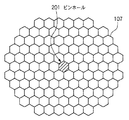
151は制御装置であり、EUV光強度検出器202による検出結果に基づき当該EUV露光装置における露光量を制御する。
図2は、上記構成における、反射型のオプティカルインテグレータ107及びその周辺の構成を説明する図である。オプティカルインテグレータ107は所定の形状を持った微小な反射面を平面または曲面上に多数配列したものである。EUV光が反射型のオプティカルインテグレータ107に入射すると、反射型のオプティカルインテグレータ107のすぐ近傍に多数の2次光源を形成する。反射型のオプティカルインテグレータが凹面ミラーを配列した形式のものであれば、2次光源は反射型のオプティカルインテグレータ反射面の外部に、反射型のオプティカルインテグレータが凸面ミラーを配列した形式のものであれば、2次光源は反射型のオプティカルインテグレータ反射面の内部に位置する。
【0044】
各2次光源から放射されたEUV光を上記照明光学系のミラーで集光してレチクル111を照明する。この2次光源がレチクル111を照明する光束の入射瞳になるように凹面ミラーを配置することによってケーラー照明を実現している。したがって反射型のオプティカルインテグレータがほぼレチクルを照明する光束の入射瞳位置になっている。
【0045】
本実施形態では、反射型のオプティカルインテグレータ107に微小なピンホール201を設ける。また、オプティカルインテグレータ107のEUV光が入射する側とは反対側にEUV光強度検出器202を設けて、ピンホール201を通過したEUV光の強度を検出する。
【0046】
EUV光強度検出器202としては、シリコンなどのフォトダイオード、蛍光体付き光電子増倍管、イオンチャンバ、光電面を設けた電子増倍管などが用いられる。EUV光強度検出器202で検出される可視光を除去するために金属の薄膜からなるフィルタ203を用いることが望ましい。
【0047】
また、半導体ダイオードは高い強度のEUV光を受光すると感度低下などの損傷が起きることが知られており、これを防止するには、受光面のEUV光強度を一定値以下に下げることが必要である。このためにも、EUV光強度検出器202の前面にフィルタ203を設けることは望ましいことである。更に、迷光などによる精度低下を防ぐためには、フィルタの材質としては、多層膜の反射率が、高い波長のEUV光は比較的良く透過し、それ以外の波長の光は吸収する材料であることが望ましい。そのようなフィルタは、ミラーの多層膜を形成する軽元素層を構成する元素を含む材料を選択することによって実現する。例えば、ミラーにモリブデンとシリコンの多層膜を用いる場合、シリコンを含んだ材料、例えばシリコン単結晶やシリコンカーバイド、窒化シリコンなどが用いられる。あるいは、ミラーにモリブデンとベリリウムの多層膜を用いる場合、ベリリウムが用いられる。
【0048】
シリコン単結晶やシリコンカーバイド、窒化シリコンなどのフィルタを用いる場合、前述したように可視光を除去するために金属の薄膜からなるフィルタ、例えばベリリウムなどと積層して用いることが望ましい。
【0049】
また、オプティカルインテグレータの1点に入射するEUV光は一定の角度広がりをもっており、ピンホール201を通過したEUV光は同じ角度で広がる。EUV光強度検出器202をピンホール201から一定距離離す構成をとれば、検出器の受光面の単位当たりのEUV光強度が低減し、感度低下などの損傷が起きることを防止できる。このときの検出器のEUV光が照射される範囲の大きさは、検出器の受光面サイズ以内でできるだけ大きくなるように検出器とピンホールとの距離を設定すればよい。
【0050】
このような構成にすることによってほぼレチクルを照明する光束の入射瞳位置でのEUV光強度を計測することができる。
【0051】
オプティカルインテグレータ107の位置はほぼレチクル111を照明する光束の入射瞳位置になっているので、ピンホール201を設けることによってレチクル111を照射する光束の入射瞳面内の分布が一様でなくなり、解像性能に影響を及ぼす。この観点からは、ピンホールの直径はできるだけ小さいことが望ましく、具体的にはインテグレータの光が照射される領域のサイズの1%以内程度が望ましい。
【0052】
反射型インテグレータ107の反射面は、微小な球面などの単位形状が多数配列した構造をしている。各単位形状から反射されたEUV光はレチクルの照明領域全面を照射する。この単位形状を例えば半分取り除く形でピンホールを設けたならば、レチクル上の照明領域の半分で照度の低下が起こり、照度分布が不均一になってしまう。したがって、単位形状が欠けない形でピンホールを設けることが望ましい。
【0053】
単位形状が欠けない形でピンホールを設ける方法としては、図3に示すように、この単位形状を1個丸ごと取り除く形でピンホールを設ければよい。あるいは、図4に示すように、単位形状の配列をずらして、隙間を開けてその隙間にピンホールを設けてもよい。以上のような方法を用いれば、ピンホールを設けてもレチクル上のEUV光照度分布に影響を与えることがない。
【0054】
また、ピンホールの断面形状は、インテグレータに入射するEUV光の角度に合わせて斜めにしたり、図2に示すように反射面の開口が小さく裏面の開口が大きい「逆テーパ状」として、EUV光がピンホール内面で遮られることがないようにするのが望ましい。
【0055】
以上のような構成を備えた本実施形態のEUV露光装置では、レチクルを照明する光束の入射瞳位置でのEUV光強度を計測し、それに基づき、レジストに照射されるEUV光の量が一定になるように制御装置151が露光量制御を行う。例えば、計測されたEUV強度が変動した場合には、光源の発光強度を変更する、あるいは光源の発光タイミングを変更する事で平均の光強度を変化させる、あるいはウエハ上の1点が露光される時間を変更する、などの方法を用いることができる。
【0056】
また、制御装置151は、計測されたEUV強度の値をもとに、プラズマ光源を構成する部品の消耗や、照明系ミラーの損傷などを検出し、それらの交換時期を判定する。これは例えば以下のようにして行われる。プラズマ光源の発光はパルス状に行われ、パルス毎の発光強度はある程度ばらつくので、多数のパルスを平均した強度を求め、この時間変化を記録する。そして、この平均強度の値が初期の値に比べて一定量、たとえば初期値の10%低下した場合には、プラズマ光源を構成する部品の消耗、あるいは照明系ミラーの損傷が起きたと判定し、これらの部品を交換するべく報知する。
【0057】
以上説明したように、本実施形態のEUV露光装置によれば、レチクルを照明する光束の入射瞳位置でのEUV光強度を計測し、それに基づき、レジストに照射されるEUV光の量が一定になるように露光量制御を行うので、EUV発光強度の変動とそれに伴う微細なパターンの寸法変化や解像度低下などが起こらず、安定して微細なパターンを転写することができる。また、プラズマ光源を構成する部品の消耗や、照明系ミラーの損傷などを検出し、それらの交換時期を的確に判定することができる。
【0058】
また、EUV光強度検出器202の前面に、金属の薄膜からなるフィルタ203および/または、ミラーの多層膜を形成する軽元素層を構成する元素を含む材料からなるフィルタを配置することにより、可視光や迷光などによる精度低下を防ぎながら、さらに検出器に感度低下などの損傷が起きることを防止できる。例えば、前述の単結晶シリコン、窒化シリコン、シリコンカーバイドなどの材料からなるフィルタは、可視光を透過する。そこで金属のフィルタを重ねて可視光をカットする。これらのフィルタは独立した別体のフィルタでもよいし、シリコン含有フィルタの上に金属薄膜を成膜した一体構成でもよい。金属フィルタの厚さが薄い場合には、一体構成のほうが製造や取り扱いの容易さの点で有利である。また、EUV光強度検出器202をピンホール201から一定距離離す構成を用いれば、検出器202の受光面の単位当たりのEUV光強度が低減し、検出器202に感度低下などの損傷が起きることを防止できる。
【0059】
<第2の実施形態>
第1の実施形態では、オプティカルインテグレータにピンホールを設けて、 レチクルを照明する光束の入射瞳位置でのEUV光強度を計測している。第2の実施形態では、オプティカルインテグレータの前面に反射ミラーを設けてレチクルを照明する光束の入射瞳位置でのEUV光強度を計測する。なお、以下の第1の実施形態では、第1の実施形態と同様にレーザプラズマ光源を用いたEUV露光装置を説明するが、放電プラズマ光源を用いたEUV露光装置に適用することも可能であることはいうまでもない。
【0060】
図5は第2の実施形態によるEUV光露光装置の概観を示す図である。第1の実施形態(図1)と同様の構成には同一の参照番号を付してある。第1の実施形態と異なる点は、オプティカルインテグレータ503にはピンホールは存在せず、その前面に微小ミラー501が設けられた点である。微小ミラー501で反射されたEUV光はEUV光強度検出器502によってその光強度が検出されることになる。なお、EUV光強度検出器502はEUV光強度検出器202と同一の機能を有するものである。また第1の実施形態と同様なフィルタ構成を用いてもよい。
【0061】
以上の構成において、プラズマ光源105から放射されたEUV光は照明系初段ミラー106で集光され、反射型のオプティカルインテグレータ503に導かれる。第2の実施形態では、図6にその詳細を示すように、反射型のオプティカルインテグレータ503の前面に微小ミラー501を設ける。そして、オプティカルインテグレータ503に入射するEUV光あるいはそこから出射するEUV光を遮らない位置に微小ミラー501からの反射光を導き、ここにEUV光強度検出器502を設けて、微小ミラーからの反射光の強度を検出する。
【0062】
微小ミラー501は、照明系や投影系のほかのミラーと同様に、研磨したガラスや金属、セラミクスからなる基板の表面に多層膜を成膜して反射率を高めてある。入射角60度程度以上の斜入射で用いられ場合には、全反射を利用しても良く、研磨したシリコンカーバイドや、研磨したガラス基板の上に白金や金の単層膜を成膜したミラーでもよい。
【0063】
また、微小ミラー501は反射型のオプティカルインテグレータに接着して固定してもよいし、反射型のオプティカルインテグレータに穴を開け、反射型のオプティカルインテグレータに裏面から支持機構を介して支持しても構わない。
【0064】
また、オプティカルインテグレータの1点に入射するEUV光は一定の角度広がりをもっている。微小ミラー501が平面であった場合、この微小ミラー501で反射されたEUV光は同じ角度で広がる。検出器502はオプティカルインテグレータ503に入射あるいは出射するEUV光を遮らない位置に置く必要があるので、微小ミラー501からの距離は一定の距離が必要である。このため、反射光のスポットの大きさは、検出器502の受光面サイズを越えてしまう場合がある。このような場合には、微小ミラー501を球面や円筒面や回転楕円面やトロイダル面などの凹面とし、反射されたEUV光の角度広がりをある程度小さくすることが好ましい。特に、検出器502のEUV光が照射される範囲の大きさを検出器502の受光面サイズ以内でできるだけ大きくなるようにすることで、検出器502の受光面における単位当たりのEUV光強度を低減し、感度低下などの損傷が起きることを防止できる。
【0065】
以上のような構成にすることによって、第1の実施形態と同様に、レチクルを照明する光束のほぼ入射瞳位置でのEUV光強度を計測することができる。
【0066】
なお、反射型インテグレータ503の反射面は、微小な球面などの単位形状が多数配列した構造をしている。各単位形状から反射されたEUV光はレチクルの照明領域全面を照射する。この単位形状を例えば半分取り除く形で微小ミラーを設けたならば、レチクル上の照明領域の半分で照度の低下が起こり、照度分布が不均一になってしまう。したがって、単位形状が欠けない形で微小ミラーを設けることが望ましい。
【0067】
単位形状が欠けない形で微小ミラーを設ける方法としては、1つの単位形状を丸ごと覆う、同形状のミラーを用いることが挙げられる。例えば、図7に示すように、単位形状が矩形であった場合、この単位形状を1個丸ごと覆う矩形の微小ミラーを設ければよい。このような方法を用いれば、微小ミラーを設けてもレチクル上のEUV光照度分布に影響を与えることがない。
【0068】
構成、第2の実施形態においても、第1の実施形態と同様に、レチクルを照明する光束の入射瞳位置でのEUV光強度を計測し、それに基づき、レジストに照射されるEUV光の量が一定になるように露光量制御を行う。また、計測されたEUV強度の値をもとに、プラズマ光源を構成する部品の消耗や、照明系ミラーの損傷などを検出し、それらの交換時期を判定する。
【0069】
第2の実施形態のEUV露光装置によれば、レチクルを照明する光束の入射瞳位置でのEUV光強度を計測し、それに基づき、レジストに照射されるEUV光の量が一定になるように露光量制御を行うので、EUV発光強度の変動とそれに伴う微細なパターンの寸法変化や解像度低下などが起こらず、安定して微細なパターンが転写転写ができるEUV光を用いた露光装置および露光方法が実現される。
【0070】
また、プラズマ光源を構成する部品の消耗や、照明系ミラーの損傷などを検出し、それらの交換時期を的確に判定することができる
更に、微小ミラー501を凹面とすることで、微小ミラーで反射されたEUV光の角度広がりをある程度小さくし、検出器502のEUV光が照射される範囲の大きさを検出器の受光面サイズ以内でできるだけ大きくなるようにし、かつ検出器の受光面の単位当たりのEUV光強度を低減したので、感度低下などの損傷が起きることを防止することができる。
【0071】
<実施形態3>
次に上記説明した露光装置を利用したデバイスの製造方法の実施例を説明する。図9は微小デバイス(ICやLSI等の半導体チップ、液晶パネル、CCD、薄膜磁気ヘッド、マイクロマシン等)の製造フローを示す。
【0072】
ステップS11(回路設計)では半導体デバイスの回路設計を行う。ステップS12(マスク製作)では設計した回路パターンを形成したマスクを制作する。一方、ステップS13(ウエハ製造)ではシリコン等の材料を用いてウエハを製造する。ステップS14(ウエハプロセス)では前工程 と呼ばれ、上記用意したマスクとウエハを用いて、リソグラフィー技術によってウエハ上に実際の回路を形成する。次にステップS15(組み立て)は後工程と呼ばれ、ステップS14によって作製されたウエハを用いて半導体チップ化する工程であり、アッセンブリ工程(ダイシング、ボンディング)、パッケージング工程(チップ封入)等の工程を含む。ステップS16(検査)ではステップS15で作製された半導体デバイスの動作確認テスト、耐久性テスト等の検査を行う。こうした工程を経て半導体デバイスが完成し、これが出荷(ステップS17)される。
【0073】
図10は上記ウエハプロセスの詳細なフローを示す。ステップS21(酸化)ではウエハの表面を酸化させる。ステップS22(CVD)ではウエハ表面に絶縁膜を形成する。ステップS23(電極形成)ではウエハ上に電極を蒸着によって形成する。ステップS24(イオン打込み)ではウエハにイオンを打ち込む。ステップS25(レジスト処理)ではウエハに感光剤を塗布する。ステップS26(露光)では上記説明した露光装置によってマスクの回路パターンをウエハに焼付露光する。ステップS27(現像)では露光したウエハを現像する。ステップS28(エッチング)では現像したレジスト像以外の部分を削り取る。ステップS29(レジスト剥離)ではエッチングが済んで不要となったレジストを取り除く。これらのステップを繰り返し行うことによって、ウエハ上に多重に回路パターンが形成される。
【0074】
本実施例の製造方法を用いれば、従来は製造が難しかった高集積度の半導体デバイスを製造することができる。
【0075】
【発明の効果】
以上説明したように、本発明によれば、露光光の強度の測定精度が向上する。又、測定された露光光強度の値を露光量制御に用いれば、露光量の補償制御が適切に行える。このため、光源における発光強度の変動等に伴う微細なパターンの寸法変化や解像度低下などを防止し、微細なパターン転写を安定的に実行するべく露光制御を行うことができる。
【図面の簡単な説明】
【図1】第1の実施形態によるEUV光露光装置の概略構成を示す図である。
【図2】第1の実施形態による反射型のオプティカルインテグレータ及びその周辺の構成を説明する図である。
【図3】第1の実施形態による反射形オプティカルインテグレータにおけるピンホールの形成を説明する図である。
【図4】第1の実施形態による反射形オプティカルインテグレータにおけるピンホールの形成を説明する図である。
【図5】第2の実施形態によるEUV光露光装置の概略構成を示す図である。
【図6】第2の実施形態による反射型のオプティカルインテグレータ及びその周辺の構成を説明する図である。
【図7】第2の実施形態による反射形オプティカルインテグレータにおける微小ミラーの形状及び配置を説明する図である。
【図8】円弧状露光領域を説明する図である。
【図9】半導体デバイスの製造フローを示す図である。
【図10】ウエハプロセスの詳細なフローを示す図である。[0001]
TECHNICAL FIELD OF THE INVENTION
The present invention relates to an exposure apparatus capable of transferring a fine circuit pattern and a control method thereof.
[0002]
[Prior art]
2. Description of the Related Art Conventionally, as a printing (lithography) method for manufacturing fine semiconductor elements such as semiconductor memories and logic circuits, reduced projection exposure using ultraviolet rays has been performed.
[0003]
The minimum dimension that can be transferred by the reduced projection exposure is proportional to the wavelength of light used for transfer, and inversely proportional to the numerical aperture of the projection optical system. Therefore, in order to transfer a fine circuit pattern, it is necessary to shorten the wavelength of light used. For this reason, the wavelength of the ultraviolet light used for the mercury lamp i-line (wavelength 365 nm), KrF excimer laser (wavelength 248 nm), and ArF excimer laser (wavelength 193 nm) is becoming shorter.
[0004]
However, semiconductor elements are rapidly miniaturized, and there is a limit in lithography using ultraviolet light. Therefore, in order to efficiently print extremely fine circuit patterns of less than 0.1 μm, a reduction projection exposure apparatus using extreme ultraviolet light (EUV light) having a shorter wavelength (about 10 to 15 nm) than ultraviolet light has been developed. Have been.
[0005]
In such an EUV light region, absorption by a substance becomes extremely large, so that a lens optical system using light refraction such as used in visible light or ultraviolet light is not practical, and in an exposure apparatus using EUV light, A reflective optical system is used. In this case, a reflective reticle having a pattern to be transferred by an absorber on a mirror is used as the reticle.
[0006]
As a reflection type optical element constituting an exposure apparatus using EUV light, there are a multilayer mirror and an oblique incidence total reflection mirror. Since the real part of the refractive index is slightly smaller than 1 in the EUV region, total reflection occurs when used at oblique incidence where EUV light is incident on the surface. Usually, a high reflectance of several tens% or more is obtained at an oblique incidence within several degrees as measured from the surface. However, the degree of freedom in optical design is small, and it is difficult to use a total reflection mirror for the projection optical system.
[0007]
As a mirror for EUV light used at an incident angle close to normal incidence, a multilayer mirror in which two kinds of substances having different optical constants are alternately stacked is used. In a multilayer mirror, molybdenum and silicon are alternately stacked on the surface of a glass substrate polished to a precise surface shape. For example, the thickness of the molybdenum layer is about 0.2 nm, the thickness of the silicon layer is about 0.5 nm, and the number of layers is about 20 layers. The sum of the thicknesses of the two types of substances is called a film cycle. In the above example, the film cycle is 0.2 nm + 0.5 nm = 0.7 nm.
[0008]
When EUV light enters such a multilayer mirror, EUV light of a specific wavelength is reflected. When the incident angle is θ, the wavelength of EUV light is λ, and the film period is d, the Bragg equation is approximately
2 × d × cos θ = λ
Only the EUV light having a narrow bandwidth centered at λ that satisfies the relationship is efficiently reflected. The bandwidth at this time is about 0.6 to 1 nm.
[0009]
The reflectance of the reflected EUV light is at most about 0.7, and the EUV light that is not reflected is absorbed in the multilayer film or the substrate, and most of the energy becomes heat.
[0010]
Multilayer mirrors used in the EUV region have a greater light loss than visible light mirrors, so it is necessary to minimize the number of mirrors. In order to realize a wide exposure area with a small number of mirrors, a reticle and a wafer are simultaneously scanned and a large area is transferred by using only a thin arc-shaped area (ring field) separated by a certain distance from the optical axis. A method (scan exposure) is conceivable.
[0011]
[Problems to be solved by the invention]
When EUV light as described above is used as exposure light, a laser plasma light source or a discharge plasma light source is used. However, such an EUV exposure apparatus has the following problems.
[0012]
A laser plasma light source used as an EUV light source irradiates a target material with high-intensity pulsed laser light to generate high-temperature plasma, and uses EUV light emitted from the plasma at a wavelength of, for example, about 13 nm. Here, the intensity of EUV light emitted from the laser plasma light source changes depending on the temperature of the target and the like. Especially in the method of increasing the gas density by adiabatic expansion of the gas or clustering the gas to obtain a high-density target, even when the emitted gas or the temperature of the nozzle is slightly changed, the excitation laser is irradiated. , The target density greatly changes, and the intensity of the emitted EUV light also changes greatly.
[0013]
When the intensity of the EUV light emitted from the light source fluctuates, the amount of the EUV light irradiated on the wafer fluctuates, and the size of the transferred fine pattern changes or the fine pattern cannot be transferred. Problems arise.
[0014]
Similarly, the intensity of EUV light emitted from the discharge plasma light source changes depending on the temperature of the electrodes and gas. The discharge plasma light source generates high-temperature plasma by applying a pulse voltage to an electrode in a gas, and uses EUV light emitted from the plasma at a wavelength of, for example, about 13 nm. Also in the discharge plasma light source, the nozzles and electrodes of the gas supply device are heated by electromagnetic waves and particles radiated from the plasma, and the electrodes are heated by Joule heat in the electrodes. For this reason, the intensity of EUV light emitted from the light source fluctuates, and accordingly, the amount of EUV light irradiated on the wafer fluctuates, so that the size of a fine pattern to be transferred changes or the fine pattern is transferred. There is a problem that it becomes impossible.
[0015]
High-temperature plasma generated by the laser plasma light source emits high-speed gas molecules and charged particles. Further, a part of the target material supply device may be hit by high-speed particles of plasma (sputtering phenomenon) and atoms on the surface may be scattered. These are called debris. When this debris is irradiated on the first stage mirror of the illumination system, the multilayer film on the mirror is damaged. The mechanism is
・ Multilayer structure is destroyed by ion energy
-The target material and the material of the target supply device are deposited on the multilayer film to form an EUV light absorbing layer
・ The film structure changes due to recrystallization and mutual diffusion of the materials constituting the film by heating the multilayer film
And so on.
[0016]
Similarly, high-speed gas molecules and charged particles are emitted from the plasma generated by the discharge plasma light source. In some cases, the electrode material or a part of the insulator material holding the electrode material is hit by high-speed particles of plasma (sputtering phenomenon) and atoms on the surface are scattered. When these debris irradiates the first stage mirror of the illumination system, the multilayer film on the mirror is damaged.
[0017]
Due to such a phenomenon, the reflectance of the multilayer mirror gradually decreases with the operation of the EUV light source, so that the intensity of the EUV light illuminating the reticle also gradually decreases. As a result, the amount of EUV light applied to the wafer fluctuates, causing a problem that the size of a fine pattern to be transferred changes and that a fine pattern cannot be transferred.
[0018]
As means for solving such a problem of illuminance fluctuation, for example, Japanese Patent Application Laid-Open No. 2000-100685 discloses an X-ray light source for generating X-rays and an illumination system for guiding X-rays from the X-ray light source to a mask. In the exposure apparatus that transfers the pattern of the mask to a photosensitive substrate, the illumination system has a plurality of reflection mirrors, with respect to the reflection surface of at least one of the plurality of reflection mirrors, There is disclosed a configuration in which a detection device for detecting electrical characteristics associated with a photoelectric effect due to the X-ray irradiation is arranged. The exposure amount is adjusted according to the detection result of the detection device, and the illuminance fluctuation of the exposure light is compensated.
[0019]
In this conventional example, a detector utilizing the photoelectric effect is arranged on the reflection surface of a reflection mirror. For this reason, the photocathode becomes very sensitive to the state of the surface, and there is a problem that the measurement sensitivity fluctuates greatly even when a very small amount of dirt adheres to the surface, and the measurement accuracy decreases.
[0020]
Also, in this conventional method, photons reflected by the mirror do not cause a photoelectric effect, and only the absorbed photons cause a photoelectric effect. Therefore, in this method, not the EUV light reflected by the mirror but the EUV light reflected by the mirror is absorbed by the mirror. Light intensity is measured. Light of various wavelengths is radiated from the EUV light source in addition to the light of the wavelength used for exposure, and the light of these wavelengths is reflected at a certain ratio even in the multilayer mirror, and passes through the inside of the illumination optical system. Therefore, in the method of arranging the detector utilizing the photoelectric effect on the reflecting surface of the reflecting mirror, the measurement accuracy is reduced due to the influence of the intensity of the light emitted from the EUV light source and not contributing to the exposure. was there.
[0021]
The present invention has been made in view of the above-described problem, and has as its object to improve the accuracy of measuring the intensity of exposure light and appropriately perform exposure amount compensation control.
Another object of the present invention is to improve the measurement accuracy of the intensity of exposure light, prevent dimensional change of a fine pattern due to fluctuation of the light emission intensity of a light source and the like, and decrease resolution, and stably transfer a fine pattern. It is an object of the present invention to realize exposure control that can be executed in a practical manner.
[0022]
[Means for Solving the Problems]
An exposure apparatus according to the present invention for achieving the above object has the following configuration. That is,
An exposure apparatus having a first reflection optical system for guiding exposure light to a reticle, and a second reflection optical system for guiding reflected light from the reticle to a substrate, and transferring a pattern on the reticle to the substrate,
The first reflection optical systemBut,
An optical integrator for uniformly illuminating the reticle with a predetermined numerical aperture,
The optical integratorProvided inPart of the exposure lightMeans to passWhen,
Passed through the passing meansDetecting means for detecting the light intensity of the exposure light.
An exposure apparatus according to another aspect of the present invention for achieving the above object has the following configuration. That is,
An exposure apparatus having a first reflection optical system for guiding exposure light to a reticle, and a second reflection optical system for guiding reflected light from the reticle to a substrate, and transferring a pattern on the reticle to the substrate,
The first reflecting optical system is:
An optical integrator for uniformly illuminating the reticle with a predetermined numerical aperture,
Detecting means for detecting the light intensity of the exposure light,
A reflection unit that reflects a part of the exposure light toward the detection unit in the vicinity of the position of the optical integrator.
[0023]
Further, a control method of the exposure apparatus according to the present invention for achieving the above object,
An optical integrator for uniformly illuminating the reticle with a predetermined numerical aperture with exposure light;Exposure lightTheA control method for an exposure apparatus, comprising: a first reflection optical system that guides a reticle to a reticle; and a second reflection optical system that guides light reflected from the reticle to a substrate, and transfers a pattern on the reticle to the substrate.
Provided in the optical integrator,Part of the exposure lightThrough the means of passingDetecting the light intensity of the exposure light,
A control step of controlling an exposure amount based on the light intensity detected by the detection step means.
Further, a control method of an exposure apparatus according to another aspect of the present invention for achieving the above object,
An optical integrator for uniformly illuminating the reticle with the exposure light at a predetermined numerical aperture, a first reflection optical system for guiding the exposure light to the reticle, and a second reflection optical system for guiding the reflection light from the reticle to the substrate An exposure apparatus having an optical system and transferring a pattern on the reticle to the substrate, comprising:
A detector provided near the position of the optical integrator and detecting the light intensity of the exposure light reflected by a reflection unit that reflects a part of the exposure light toward a detector that detects the intensity of the exposure light. Process and
A control step of controlling an exposure amount based on the light intensity detected by the detection step means.
Further, according to the present invention, there is provided a method of manufacturing a device, comprising developing a substrate exposed using the above-described exposure apparatus and forming a circuit on the substrate.
[0024]
BEST MODE FOR CARRYING OUT THE INVENTION
Hereinafter, preferred embodiments of the present invention will be described with reference to the accompanying drawings.
[0025]
<First embodiment>
In the EUV exposure apparatus of the present embodiment, the intensity of EUV light is measured in order to control the amount of exposure and to determine mirror damage. This measurement is performed by partially illuminating the illumination light at the position of the reflection-type integrator of the illumination optical system and detecting this with an EUV light intensity detector, as described later.
[0026]
FIG. 1 is a diagram showing a schematic configuration of an EUV light exposure apparatus according to the first embodiment. As shown, the EUV exposure apparatus of the present embodiment includes an EUV light source, an illumination optical system, a reflective reticle, a projection optical system, a reticle stage, a wafer stage, an alignment optical system, a vacuum system, and the like.
[0027]
A laser plasma light source is used as the EUV light source of the present embodiment. In this method, a high-intensity pulsed laser beam is irradiated to a target material supplied into a
[0028]
It goes without saying that a discharge plasma light source can be used as the EUV light source. The discharge plasma light source emits a gas around the electrode placed in a vacuum vessel, applies a pulse voltage to the electrode to cause a discharge to generate high-temperature plasma, and emits EUV light having a wavelength of, for example, about 13 nm. Is used. In order to increase the average intensity of the emitted EUV light, the higher the repetition frequency of the discharge, the better, and it is usually operated at a repetition frequency of several kHz.
[0029]
The illumination optical system includes a plurality of multilayer films or oblique incidence mirrors and an optical integrator. The illumination optical system guides the EUV light emitted from the plasma 105 by the illumination system first mirror 106, the
[0030]
The first-stage condensing mirror (illumination system first mirror) 106 plays a role of collecting EUV light emitted almost isotropically from the laser plasma 105. The
[0031]
The reticle is irradiated by the arc-shaped exposure area, and the reflected light is irradiated on the wafer via the projection optical system. Multilayer mirrors have a large loss of light compared to visible light mirrors, so it is necessary to minimize the number of mirrors. A method in which a reticle and a wafer are simultaneously scanned and a large area is transferred (scan exposure) using only a thin arc-shaped region (ring field) separated by a predetermined distance is used (see FIG. 8).
[0032]
A plurality of mirrors are also used for the projection optical system. In FIG. 1, reflected light from the reticle 111 is guided onto the
[0033]
Each mirror is ground and polished on a substrate made of a material such as low-expansion glass or silicon carbide, which has high rigidity, high hardness, and low thermal expansion coefficient, to create a predetermined reflection surface shape. / A multilayer film such as silicon is formed. If the angle of incidence is not constant depending on the location in the mirror surface, as is clear from the Bragg equation, the wavelength of EUV light whose reflectance increases with location in a multilayer film having a constant film cycle shifts. Therefore, it is necessary to have a film period distribution so that EUV light of the same wavelength is efficiently reflected within the mirror surface.
[0034]
The reticle stage 112 and the wafer stage 132 have a mechanism for synchronously scanning at a speed ratio proportional to the reduction magnification. Here, the scanning direction within the reticle or wafer surface is X, the direction perpendicular thereto is Y, and the direction perpendicular to the reticle or wafer surface is Z.
[0035]
Reticle 111 is held by reticle chuck 113 on reticle stage 112. The reticle stage 112 has a mechanism for moving at high speed in the X direction. Further, the reticle 111 has a fine movement mechanism in the X direction, the Y direction, the Z direction, and the rotation direction around each axis so that the reticle 111 can be positioned. The position and orientation of the reticle stage are measured by a laser interferometer, and the position and orientation are controlled based on the results.
[0036]
The
[0037]
The alignment detection mechanisms 114 and 134 measure the positional relationship between the position of the reticle 111 and the optical axis of the projection optical system, and the positional relationship between the position of the
[0038]
In addition, the focus position in the Z direction is measured on the wafer surface by the focus position detection mechanism 135, and the position and angle of the wafer stage 132 are controlled so that the wafer surface is always kept at the image forming position by the projection optical system during exposure.
[0039]
After one scan exposure on the
[0040]
In this manner, the operation of synchronously scanning the reduced projection image of the reticle and the image formed on the wafer is repeated (step and scan), and the transfer pattern of the reticle is transferred to the entire surface of the wafer.
[0041]
EUV light is strongly absorbed by the gas. For example, when EUV light having a wavelength of 13 nm propagates 1 m in a space filled with 10 Pa of air, about 50% of the EUV light is absorbed. To avoid gas absorption, the space in which EUV light propagates should be at least 10-1Pa or less, preferably 10-3It is necessary to keep the pressure at Pa or lower.
[0042]
Also, if carbon-containing molecules such as hydrocarbons remain in the space where the optical element to be irradiated with EUV light is placed, carbon gradually adheres to the surface of the optical element by light irradiation, and this absorbs EUV light. However, there is a problem that the reflectance is lowered. In order to prevent this carbon deposition, the space in which the optical element to be irradiated with EUV light is placed must be at least 10-4Pa or less, preferably 10-6It is necessary to keep the pressure at Pa or lower. For this reason, the light source, the optical elements of the illumination system and the projection system optical system, the reticle, the wafer, and the like are placed in the
[0043]
FIG. 2 is a diagram illustrating the configuration of the reflection type
[0044]
The EUV light emitted from each secondary light source is condensed by the mirror of the illumination optical system and illuminates the reticle 111. Koehler illumination is realized by arranging a concave mirror so that the secondary light source becomes an entrance pupil of a light beam illuminating the reticle 111. Therefore, the reflection type optical integrator is almost at the entrance pupil position of the light beam illuminating the reticle.
[0045]
In this embodiment, a
[0046]
As the EUV
[0047]
In addition, it is known that a semiconductor diode receives high-intensity EUV light to cause damage such as a reduction in sensitivity. To prevent this, it is necessary to lower the EUV light intensity on the light receiving surface to a certain value or less. is there. For this reason, it is desirable to provide a
[0048]
When a filter made of silicon single crystal, silicon carbide, silicon nitride, or the like is used, it is preferable to use a filter made of a metal thin film, such as beryllium, for removing visible light, as described above.
[0049]
The EUV light incident on one point of the optical integrator has a certain angular spread, and the EUV light that has passed through the
[0050]
With this configuration, it is possible to measure the EUV light intensity at the entrance pupil position of the light beam that illuminates the reticle.
[0051]
Since the position of the
[0052]
The reflective surface of the
[0053]
As shown in FIG. 3, a pinhole may be provided in such a manner that the unit shape is not missing, as shown in FIG. Alternatively, as shown in FIG. 4, the arrangement of the unit shapes may be shifted to form a gap, and a pinhole may be provided in the gap. By using the above-described method, even if the pinhole is provided, it does not affect the EUV light illuminance distribution on the reticle.
[0054]
Further, the cross-sectional shape of the pinhole may be made oblique according to the angle of the EUV light incident on the integrator, or as “an inversely tapered shape” as shown in FIG. However, it is desirable not to be blocked by the inner surface of the pinhole.
[0055]
In the EUV exposure apparatus of the present embodiment having the above-described configuration, the EUV light intensity at the entrance pupil position of the light beam illuminating the reticle is measured, and based on the measured intensity, the amount of EUV light irradiated on the resist is kept constant. The
[0056]
Further, based on the measured EUV intensity value, the
[0057]
As described above, according to the EUV exposure apparatus of the present embodiment, the EUV light intensity at the entrance pupil position of the light beam that illuminates the reticle is measured, and based on the measured intensity, the amount of EUV light applied to the resist is kept constant. Since the exposure amount control is performed as described above, it is possible to stably transfer a fine pattern without causing a change in EUV emission intensity and a dimensional change of the fine pattern and a reduction in resolution accompanying the fluctuation. In addition, it is possible to detect wear of components constituting the plasma light source, damage to the illumination system mirror, and the like, and accurately determine when to replace them.
[0058]
In addition, by disposing a
[0059]
<Second embodiment>
In the first embodiment, a pinhole is provided in the optical integrator, and the EUV light intensity at the entrance pupil position of the light beam illuminating the reticle is measured. In the second embodiment, a reflection mirror is provided in front of an optical integrator to measure the EUV light intensity at the entrance pupil position of a light beam illuminating the reticle. In the following first embodiment, an EUV exposure apparatus using a laser plasma light source will be described as in the first embodiment, but the present invention can also be applied to an EUV exposure apparatus using a discharge plasma light source. Needless to say.
[0060]
FIG. 5 is a diagram showing an overview of an EUV light exposure apparatus according to the second embodiment. The same components as those in the first embodiment (FIG. 1) are denoted by the same reference numerals. The difference from the first embodiment is that the
[0061]
In the above configuration, the EUV light emitted from the plasma light source 105 is collected by the illumination system first-stage mirror 106 and guided to the reflection type
[0062]
The
[0063]
Further, the
[0064]
EUV light incident on one point of the optical integrator has a certain angular spread. When the
[0065]
With the above configuration, similarly to the first embodiment, the EUV light intensity of the light beam illuminating the reticle at the almost entrance pupil position can be measured.
[0066]
The reflective surface of the
[0067]
As a method of providing a micromirror in such a manner that a unit shape is not missing, there is a method of using a mirror having the same shape that covers one whole unit shape. For example, as shown in FIG. 7, when the unit shape is a rectangle, a rectangular micromirror that covers the entire unit shape may be provided. By using such a method, even if the micro mirror is provided, the EUV light illuminance distribution on the reticle is not affected.
[0068]
In the configuration and the second embodiment, similarly to the first embodiment, the EUV light intensity at the entrance pupil position of the light beam for illuminating the reticle is measured, and the amount of the EUV light irradiated on the resist is determined based on the measured intensity. Exposure amount control is performed so as to be constant. Further, based on the measured value of the EUV intensity, wear of components constituting the plasma light source, damage to the illumination system mirror, and the like are detected, and the time to replace them is determined.
[0069]
According to the EUV exposure apparatus of the second embodiment, the EUV light intensity at the entrance pupil position of the light beam illuminating the reticle is measured, and the exposure is performed based on the measured intensity so that the amount of EUV light applied to the resist becomes constant. Since the amount control is performed, the exposure apparatus and the exposure method using EUV light, which can stably transfer a fine pattern without fluctuation of the EUV emission intensity and the dimensional change of the fine pattern and the decrease in resolution due to the fluctuation, are not provided. Is achieved.
[0070]
In addition, it is possible to detect wear of components constituting the plasma light source, damage to the illumination system mirror, and the like, and accurately determine when to replace them.
Further, by making the
[0071]
<Embodiment 3>
Next, an embodiment of a device manufacturing method using the above-described exposure apparatus will be described. FIG. 9 shows a manufacturing flow of a microdevice (a semiconductor chip such as an IC or LSI, a liquid crystal panel, a CCD, a thin-film magnetic head, a micromachine, etc.).
[0072]
In step S11 (circuit design), the circuit of the semiconductor device is designed. In step S12 (mask production), a mask on which the designed circuit pattern is formed is produced. On the other hand, in step S13 (wafer manufacturing), a wafer is manufactured using a material such as silicon. In step S14 (wafer process), which is called a pre-process, an actual circuit is formed on the wafer by lithography using the prepared mask and wafer. Next, step S15 (assembly) is called a post-process, and is a process of forming a semiconductor chip using the wafer prepared in step S14, and includes processes such as an assembly process (dicing and bonding) and a packaging process (chip encapsulation). including. In step S16 (inspection), inspections such as an operation check test and a durability test of the semiconductor device manufactured in step S15 are performed. Through these steps, a semiconductor device is completed and shipped (step S17).
[0073]
FIG. 10 shows a detailed flow of the wafer process. In step S21 (oxidation), the surface of the wafer is oxidized. In step S22 (CVD), an insulating film is formed on the wafer surface. In step S23 (electrode formation), electrodes are formed on the wafer by vapor deposition. In step S24 (ion implantation), ions are implanted into the wafer. In step S25 (resist processing), a photosensitive agent is applied to the wafer. In step S26 (exposure), the circuit pattern of the mask is printed and exposed on the wafer by the exposure apparatus described above. In step S27 (developing), the exposed wafer is developed. In step S28 (etching), portions other than the developed resist image are removed. In step S29 (resist stripping), unnecessary resist after etching is removed. By repeating these steps, multiple circuit patterns are formed on the wafer.
[0074]
By using the manufacturing method of this embodiment, it is possible to manufacture a highly integrated semiconductor device which has been conventionally difficult to manufacture.
[0075]
【The invention's effect】
As described above, according to the present invention, the accuracy of measuring the intensity of exposure light is improved. If the measured value of the exposure light intensity is used for the exposure control, the compensation control of the exposure can be appropriately performed. Therefore, it is possible to prevent a fine pattern dimensional change and a decrease in resolution due to a change in light emission intensity of the light source and the like, and to perform exposure control to stably execute a fine pattern transfer.
[Brief description of the drawings]
FIG. 1 is a diagram showing a schematic configuration of an EUV light exposure apparatus according to a first embodiment.
FIG. 2 is a diagram illustrating a configuration of a reflection-type optical integrator according to the first embodiment and a configuration around the reflection-type optical integrator;
FIG. 3 is a diagram illustrating the formation of a pinhole in the reflection type optical integrator according to the first embodiment.
FIG. 4 is a diagram illustrating the formation of a pinhole in the reflection type optical integrator according to the first embodiment.
FIG. 5 is a diagram illustrating a schematic configuration of an EUV light exposure apparatus according to a second embodiment.
FIG. 6 is a diagram illustrating a configuration of a reflection-type optical integrator according to a second embodiment and a peripheral configuration thereof;
FIG. 7 is a diagram illustrating the shape and arrangement of micromirrors in a reflective optical integrator according to a second embodiment.
FIG. 8 is a diagram illustrating an arc-shaped exposure region.
FIG. 9 is a diagram showing a manufacturing flow of the semiconductor device.
FIG. 10 is a diagram showing a detailed flow of a wafer process.
Claims (17)
前記第1反射光学系が、
前記レチクルを均一に所定の開口数で照明するためのオプティカルインテグレータと、
前記オプティカルインテグレータに設けられ、前記露光光の一部を通過させる手段と、
前記通過させる手段を通過した露光光の光強度を検出する検出手段とを備えることを特徴とする露光装置。An exposure apparatus having a first reflection optical system for guiding exposure light to a reticle, and a second reflection optical system for guiding reflected light from the reticle to a substrate, and transferring a pattern on the reticle to the substrate,
The first reflecting optical system is:
An optical integrator for uniformly illuminating the reticle with a predetermined numerical aperture,
Means provided in the optical integrator and passing a part of the exposure light,
An exposure apparatus comprising: a detection unit configured to detect a light intensity of the exposure light passing through the passing unit.
前記第1反射光学系が、
前記レチクルを均一に所定の開口数で照明するためのオプティカルインテグレータと、
露光光の光強度を検出する検出手段と、
前記オプティカルインテグレータの位置の近傍で前記露光光の一部を前記検出手段に向けて反射する反射手段とを備えることを特徴とする露光装置。An exposure apparatus having a first reflection optical system for guiding exposure light to a reticle, and a second reflection optical system for guiding reflected light from the reticle to a substrate, and transferring a pattern on the reticle to the substrate,
The first reflecting optical system is:
An optical integrator for uniformly illuminating the reticle with a predetermined numerical aperture,
Detecting means for detecting the light intensity of the exposure light,
An exposure apparatus, comprising: a reflection unit that reflects a part of the exposure light toward the detection unit near a position of the optical integrator.
前記オプティカルインテグレータに設けられ、前記露光光の一部を通過させる手段を通過した露光光の光強度を検出する検出工程と、
前記検出工程手段で検出された光強度に基づいて露光量を制御する制御工程とを備えることを特徴とする露光装置の制御方法。 It has an optical integrator for illuminating a reticle uniformly with a predetermined aperture by exposure light, a first reflection optical system for guiding the exposure light to the reticle, a second reflection that leads to substrate reflected light from said reticle An exposure apparatus having an optical system and transferring a pattern on the reticle to the substrate, comprising:
Provided in the optical integrator, a detection step of detecting the light intensity of the exposure light passed through the means for passing a portion of the exposure light
A control step of controlling an exposure amount based on the light intensity detected by the detection step means.
前記オプティカルインテグレータの位置の近傍に設けられ、前記露光光の一部を露光光強度を検出する検出器に向けて反射する反射手段によって反射された露光光の光強度を該検出器により検出する検出工程と、
前記検出工程手段で検出された光強度に基づいて露光量を制御する制御工程とを備えることを特徴とする露光装置の制御方法。 It has an optical integrator for illuminating a reticle uniformly with a predetermined aperture by exposure light, a first reflection optical system for guiding the exposure light to the reticle, a second reflection that leads to substrate reflected light from said reticle An exposure apparatus having an optical system and transferring a pattern on the reticle to the substrate, comprising:
Provided in the vicinity of the position of the optical integrator, detection detected by the detector the light intensity of the exposure light reflected by the reflecting means for reflecting a portion of the exposure light to a detector for detecting the exposure light intensity Process and
A control step of controlling an exposure amount based on the light intensity detected by the detection step means.
Priority Applications (3)
| Application Number | Priority Date | Filing Date | Title |
|---|---|---|---|
| JP2002020213A JP3564104B2 (en) | 2002-01-29 | 2002-01-29 | Exposure apparatus, control method therefor, and device manufacturing method using the same |
| US10/351,416 US6825481B2 (en) | 2002-01-29 | 2003-01-27 | Exposure apparatus, control method thereof, and device manufacturing method using the same |
| EP03250552A EP1331519A3 (en) | 2002-01-29 | 2003-01-29 | Exposure control |
Applications Claiming Priority (1)
| Application Number | Priority Date | Filing Date | Title |
|---|---|---|---|
| JP2002020213A JP3564104B2 (en) | 2002-01-29 | 2002-01-29 | Exposure apparatus, control method therefor, and device manufacturing method using the same |
Publications (2)
| Publication Number | Publication Date |
|---|---|
| JP2003224053A JP2003224053A (en) | 2003-08-08 |
| JP3564104B2 true JP3564104B2 (en) | 2004-09-08 |
Family
ID=19192156
Family Applications (1)
| Application Number | Title | Priority Date | Filing Date |
|---|---|---|---|
| JP2002020213A Expired - Fee Related JP3564104B2 (en) | 2002-01-29 | 2002-01-29 | Exposure apparatus, control method therefor, and device manufacturing method using the same |
Country Status (3)
| Country | Link |
|---|---|
| US (1) | US6825481B2 (en) |
| EP (1) | EP1331519A3 (en) |
| JP (1) | JP3564104B2 (en) |
Families Citing this family (34)
| Publication number | Priority date | Publication date | Assignee | Title |
|---|---|---|---|---|
| AU2002239826A1 (en) * | 2001-01-09 | 2002-07-24 | Whitehead Institute For Biomedical Research | Methods and reagents for the isolation of nucleic acids |
| JP2004061177A (en) * | 2002-07-25 | 2004-02-26 | Canon Inc | Optical device and measuring method, and manufacturing method of semiconductor device |
| WO2004031854A2 (en) * | 2002-09-30 | 2004-04-15 | Carl Zeiss Smt Ag | Illumination system for a wavelength = 193 nm, comprising sensors for determining the illumination |
| EP1426824A1 (en) | 2002-12-04 | 2004-06-09 | ASML Netherlands B.V. | Lithographic apparatus, device manufacturing method, and device manufactured thereby |
| EP1426827A1 (en) * | 2002-12-04 | 2004-06-09 | ASML Netherlands B.V. | Lithographic apparatus, device manufacturing method, and device manufactured thereby |
| JP4262032B2 (en) * | 2003-08-25 | 2009-05-13 | キヤノン株式会社 | EUV light source spectrum measurement device |
| JP2005141158A (en) * | 2003-11-10 | 2005-06-02 | Canon Inc | Illumination optical system and aligner |
| JP2005317611A (en) * | 2004-04-27 | 2005-11-10 | Canon Inc | Exposure method and aligner |
| JP4645358B2 (en) * | 2004-08-20 | 2011-03-09 | ソニー株式会社 | Imaging apparatus and imaging method |
| JP2006134974A (en) | 2004-11-04 | 2006-05-25 | Canon Inc | Exposure device, judgment method and device manufacturing method |
| US7329884B2 (en) * | 2004-11-08 | 2008-02-12 | Nikon Corporation | Exposure apparatus and exposure method |
| US7372623B2 (en) | 2005-03-29 | 2008-05-13 | Asml Netherlands B.V. | Multi-layer spectral purity filter, lithographic apparatus including such a spectral purity filter, device manufacturing method, and device manufactured thereby |
| DE102005016591B4 (en) * | 2005-04-11 | 2009-11-26 | Fraunhofer-Gesellschaft zur Förderung der angewandten Forschung e.V. | Transmission filter for the EUV spectral range |
| KR101267144B1 (en) * | 2005-05-23 | 2013-05-23 | 가부시키가이샤 니콘 | Sensor calibration method, exposure method, exposure device, device fabrication method, and reflection type mask |
| US7365349B2 (en) * | 2005-06-27 | 2008-04-29 | Cymer, Inc. | EUV light source collector lifetime improvements |
| US7812928B2 (en) * | 2005-07-06 | 2010-10-12 | Nikon Corporation | Exposure apparatus |
| KR101370203B1 (en) * | 2005-11-10 | 2014-03-05 | 칼 짜이스 에스엠테 게엠베하 | Euv illumination system with a system for measuring fluctuations of the light source |
| US7862961B2 (en) * | 2006-02-16 | 2011-01-04 | Nikon Corporation | Mask and exposure apparatus |
| WO2007094197A1 (en) * | 2006-02-16 | 2007-08-23 | Nikon Corporation | Protection device, mask, and exposure device |
| US7936445B2 (en) * | 2006-06-19 | 2011-05-03 | Asml Netherlands B.V. | Altering pattern data based on measured optical element characteristics |
| US7541603B2 (en) | 2006-09-27 | 2009-06-02 | Asml Netherlands B.V. | Radiation system and lithographic apparatus comprising the same |
| US7916274B2 (en) | 2006-10-27 | 2011-03-29 | Nikon Corporation | Measurement of EUV intensity |
| US20090040493A1 (en) * | 2007-08-09 | 2009-02-12 | Hideki Komatsuda | Illumination optical system, illumination optical apparatus, exposure apparatus, and device manufacturing method |
| US7960701B2 (en) * | 2007-12-20 | 2011-06-14 | Cymer, Inc. | EUV light source components and methods for producing, using and refurbishing same |
| DE102008017645A1 (en) | 2008-04-04 | 2009-10-08 | Carl Zeiss Smt Ag | Apparatus for microlithographic projection exposure and apparatus for inspecting a surface of a substrate |
| JP2010123714A (en) * | 2008-11-19 | 2010-06-03 | Ushio Inc | Extreme ultraviolet light source device |
| DE102009030230A1 (en) * | 2009-06-23 | 2010-12-30 | Carl Zeiss Smt Ag | Reflective optical element with a measuring device |
| DE102010006326A1 (en) * | 2010-01-29 | 2011-08-04 | Asml Netherlands B.V. | Arrangement for use in a projection exposure apparatus for microlithography with a reflective optical element |
| JP2012129345A (en) * | 2010-12-15 | 2012-07-05 | Renesas Electronics Corp | Method of manufacturing semiconductor device, exposure method and exposure device |
| JP2014514736A (en) * | 2011-03-16 | 2014-06-19 | ケーエルエー−テンカー コーポレイション | EUV Actinic Reticle Inspection System Using Image Sensor with Thin Film Spectral Purity Filter Coating |
| DE102014223411A1 (en) * | 2014-11-17 | 2016-05-19 | Carl Zeiss Smt Gmbh | Arrangement and method for measuring the intensity of electromagnetic radiation in an optical system |
| DE102016201485B3 (en) * | 2016-02-01 | 2017-04-13 | Fraunhofer-Gesellschaft zur Förderung der angewandten Forschung e.V. | Arrangement and method for wavefront analysis |
| JP2020177105A (en) * | 2019-04-17 | 2020-10-29 | 株式会社ブイ・テクノロジー | Exposure mirror, method for manufacturing exposure mirror, and exposure apparatus including exposure mirror |
| WO2024188550A1 (en) * | 2023-03-14 | 2024-09-19 | Asml Netherlands B.V. | Methods and systems for determining a property of euv radiation |
Family Cites Families (15)
| Publication number | Priority date | Publication date | Assignee | Title |
|---|---|---|---|---|
| JPS6372116A (en) | 1986-09-16 | 1988-04-01 | Hitachi Ltd | X-ray exposure device |
| JPH0820518B2 (en) | 1987-02-26 | 1996-03-04 | キヤノン株式会社 | Exposure equipment |
| US5222112A (en) | 1990-12-27 | 1993-06-22 | Hitachi, Ltd. | X-ray pattern masking by a reflective reduction projection optical system |
| US5394451A (en) | 1991-10-08 | 1995-02-28 | Canon Kabushiki Kaisha | Optical arrangement for exposure apparatus |
| US6400444B2 (en) * | 1992-07-09 | 2002-06-04 | Canon Kabushiki Kaisha | Exposure apparatus and device producing method using the same |
| DE69322345T2 (en) | 1992-09-14 | 1999-05-20 | Canon K.K., Tokio/Tokyo | Synchrotron X-ray exposure process |
| US6038279A (en) | 1995-10-16 | 2000-03-14 | Canon Kabushiki Kaisha | X-ray generating device, and exposure apparatus and semiconductor device production method using the X-ray generating device |
| JP3284045B2 (en) | 1996-04-30 | 2002-05-20 | キヤノン株式会社 | X-ray optical apparatus and device manufacturing method |
| JP3706691B2 (en) | 1996-08-26 | 2005-10-12 | キヤノン株式会社 | X-ray reduction projection exposure apparatus and semiconductor device manufacturing method using the same |
| JP3689516B2 (en) | 1997-01-29 | 2005-08-31 | キヤノン株式会社 | Electron beam exposure system |
| JP3005203B2 (en) | 1997-03-24 | 2000-01-31 | キヤノン株式会社 | Illumination apparatus, exposure apparatus, and device manufacturing method |
| DE19724903A1 (en) | 1997-06-12 | 1998-12-17 | Zeiss Carl Fa | Light intensity measuring arrangement |
| JP2000100685A (en) | 1998-09-17 | 2000-04-07 | Nikon Corp | Aligner and exposure method using the same |
| JP2000349009A (en) * | 1999-06-04 | 2000-12-15 | Nikon Corp | Exposure method and aligner |
| JP2001110710A (en) * | 1999-10-08 | 2001-04-20 | Nikon Corp | Aligner, exposing method and manufacturing method of semiconductor device |
-
2002
- 2002-01-29 JP JP2002020213A patent/JP3564104B2/en not_active Expired - Fee Related
-
2003
- 2003-01-27 US US10/351,416 patent/US6825481B2/en not_active Expired - Fee Related
- 2003-01-29 EP EP03250552A patent/EP1331519A3/en not_active Withdrawn
Also Published As
| Publication number | Publication date |
|---|---|
| EP1331519A2 (en) | 2003-07-30 |
| JP2003224053A (en) | 2003-08-08 |
| US20030142410A1 (en) | 2003-07-31 |
| EP1331519A3 (en) | 2004-01-21 |
| US6825481B2 (en) | 2004-11-30 |
Similar Documents
| Publication | Publication Date | Title |
|---|---|---|
| JP3564104B2 (en) | Exposure apparatus, control method therefor, and device manufacturing method using the same | |
| JP4373987B2 (en) | Sensors used in lithographic apparatus | |
| US7091507B2 (en) | Light generator and exposure apparatus | |
| KR101572930B1 (en) | Radiation system, radiation collector, radiation beam conditioning system, spectral purity filter for a radiation system and method of forming a spectral purity filter | |
| US7362416B2 (en) | Exposure apparatus, evaluation method and device fabrication method | |
| US20090072167A1 (en) | Exposure apparatus, light source apparatus and device fabrication | |
| KR100911223B1 (en) | Measuring apparatus, exposure apparatus and method, and device manufacturing method | |
| JP2002353099A (en) | Apparatus and method for detecting position aligner and method for manufacturing device | |
| US8431916B2 (en) | Radiation source and lithographic apparatus | |
| KR100696736B1 (en) | Lithographic projection apparatus having a collector including concave and convex mirrors | |
| KR20020016543A (en) | Lithographic apparatus, device manufacturing method, and device manufactured thereby | |
| EP1589792B1 (en) | Light source apparatus and exposure apparatus having the same | |
| EP1387220A2 (en) | Adjustment method and apparatus of optical system, and exposure apparatus | |
| JP2010258447A (en) | Lithographic radiation source, collector, apparatus and method | |
| JP5223921B2 (en) | Illumination optical system, exposure apparatus, and exposure method | |
| US20110199600A1 (en) | Collector assembly, radiation source, lithographic apparatus and device manufacturing method | |
| US20110188018A1 (en) | Alignment of Collector Device in Lithographic Apparatus | |
| EP1617292B1 (en) | Light source unit and exposure apparatus having the same | |
| JP3782736B2 (en) | Exposure apparatus and control method thereof | |
| WO2005096680A1 (en) | Light source unit, illumination optical device and exposing method | |
| JP3874755B2 (en) | Method for determining stray radiation, lithographic projection apparatus | |
| US7102734B2 (en) | Exposure apparatus | |
| JP2004273926A (en) | Aligner | |
| JP2005011914A (en) | Reflector type mask and aligner | |
| US6833905B2 (en) | Illumination apparatus, projection exposure apparatus, and device fabricating method |
Legal Events
| Date | Code | Title | Description |
|---|---|---|---|
| A131 | Notification of reasons for refusal |
Free format text: JAPANESE INTERMEDIATE CODE: A131 Effective date: 20040206 |
|
| A521 | Written amendment |
Free format text: JAPANESE INTERMEDIATE CODE: A523 Effective date: 20040406 |
|
| TRDD | Decision of grant or rejection written | ||
| A01 | Written decision to grant a patent or to grant a registration (utility model) |
Free format text: JAPANESE INTERMEDIATE CODE: A01 Effective date: 20040521 |
|
| A61 | First payment of annual fees (during grant procedure) |
Free format text: JAPANESE INTERMEDIATE CODE: A61 Effective date: 20040604 |
|
| R150 | Certificate of patent or registration of utility model |
Free format text: JAPANESE INTERMEDIATE CODE: R150 |
|
| FPAY | Renewal fee payment (event date is renewal date of database) |
Free format text: PAYMENT UNTIL: 20080611 Year of fee payment: 4 |
|
| FPAY | Renewal fee payment (event date is renewal date of database) |
Free format text: PAYMENT UNTIL: 20090611 Year of fee payment: 5 |
|
| FPAY | Renewal fee payment (event date is renewal date of database) |
Free format text: PAYMENT UNTIL: 20090611 Year of fee payment: 5 |
|
| FPAY | Renewal fee payment (event date is renewal date of database) |
Free format text: PAYMENT UNTIL: 20100611 Year of fee payment: 6 |
|
| FPAY | Renewal fee payment (event date is renewal date of database) |
Free format text: PAYMENT UNTIL: 20110611 Year of fee payment: 7 |
|
| FPAY | Renewal fee payment (event date is renewal date of database) |
Free format text: PAYMENT UNTIL: 20120611 Year of fee payment: 8 |
|
| FPAY | Renewal fee payment (event date is renewal date of database) |
Free format text: PAYMENT UNTIL: 20120611 Year of fee payment: 8 |
|
| FPAY | Renewal fee payment (event date is renewal date of database) |
Free format text: PAYMENT UNTIL: 20130611 Year of fee payment: 9 |
|
| LAPS | Cancellation because of no payment of annual fees |