JP3556315B2 - Display device and semiconductor element - Google Patents
Display device and semiconductor element Download PDFInfo
- Publication number
- JP3556315B2 JP3556315B2 JP05960595A JP5960595A JP3556315B2 JP 3556315 B2 JP3556315 B2 JP 3556315B2 JP 05960595 A JP05960595 A JP 05960595A JP 5960595 A JP5960595 A JP 5960595A JP 3556315 B2 JP3556315 B2 JP 3556315B2
- Authority
- JP
- Japan
- Prior art keywords
- driving semiconductor
- semiconductor element
- wiring
- input
- display device
- Prior art date
- Legal status (The legal status is an assumption and is not a legal conclusion. Google has not performed a legal analysis and makes no representation as to the accuracy of the status listed.)
- Expired - Fee Related
Links
Images


Classifications
-
- G—PHYSICS
- G02—OPTICS
- G02F—OPTICAL DEVICES OR ARRANGEMENTS FOR THE CONTROL OF LIGHT BY MODIFICATION OF THE OPTICAL PROPERTIES OF THE MEDIA OF THE ELEMENTS INVOLVED THEREIN; NON-LINEAR OPTICS; FREQUENCY-CHANGING OF LIGHT; OPTICAL LOGIC ELEMENTS; OPTICAL ANALOGUE/DIGITAL CONVERTERS
- G02F1/00—Devices or arrangements for the control of the intensity, colour, phase, polarisation or direction of light arriving from an independent light source, e.g. switching, gating or modulating; Non-linear optics
- G02F1/01—Devices or arrangements for the control of the intensity, colour, phase, polarisation or direction of light arriving from an independent light source, e.g. switching, gating or modulating; Non-linear optics for the control of the intensity, phase, polarisation or colour
- G02F1/13—Devices or arrangements for the control of the intensity, colour, phase, polarisation or direction of light arriving from an independent light source, e.g. switching, gating or modulating; Non-linear optics for the control of the intensity, phase, polarisation or colour based on liquid crystals, e.g. single liquid crystal display cells
- G02F1/133—Constructional arrangements; Operation of liquid crystal cells; Circuit arrangements
- G02F1/1333—Constructional arrangements; Manufacturing methods
- G02F1/1345—Conductors connecting electrodes to cell terminals
- G02F1/13452—Conductors connecting driver circuitry and terminals of panels
-
- H10W70/611—
-
- H10W70/688—
Landscapes
- Physics & Mathematics (AREA)
- Nonlinear Science (AREA)
- Mathematical Physics (AREA)
- Chemical & Material Sciences (AREA)
- Crystallography & Structural Chemistry (AREA)
- General Physics & Mathematics (AREA)
- Optics & Photonics (AREA)
- Devices For Indicating Variable Information By Combining Individual Elements (AREA)
- Liquid Crystal (AREA)
- Wire Bonding (AREA)
Description
【0001】
【産業上の利用分野】
本発明は基板上に表示部と、これを駆動する駆動用半導体素子が同時に形成された表示装置に係り、特に駆動用半導体素子の配線の取り出し方に特徴を有する表示装置に係わる。
【0002】
【従来技術】
液晶表示装置、プラズマ表示装置等、マトリックス状に画素分割され、それぞれの画素を駆動用半導体素子で時系列的に駆動する表示装置では、画素の高精細化に伴い、駆動用半導体素子を微細ピッチ配線に接続する接続方法が問題になってきた。
【0003】
微細ピッチ接続に対応した技術として、COG(Chip on glass )、COF(Chip on film)と呼ばれる、基板上に形成された配線上に、駆動用半導体素子をフェイスダウンで実装する方法が開発されている。
【0004】
図17にガラス基板上に駆動用半導体素子を実装した従来のCOG実装を用いた表示装置の概略図を示す。
ガラス基板100上に表示部101が形成されており、この表示部101から駆動用の配線102が延びている。この配線102に駆動用半導体素子103がフェイスダウンで実装されている。この駆動用半導体素子103を駆動するための入力配線104は駆動用半導体素子103の表示部101とは反対側の辺から基板外側に延びており、フレキシブル配線基板105に接続される。フレキシブル基板105は、フレキシブル基板105を介して画像用LSI106などが搭載されている回路基板107に接続され表示装置を構成している。
【0005】
図18に駆動用半導体素子103を配線上にCOG実装した部分を拡大した図を示す。
駆動用半導体素子103は4辺を有する四角形をしており、4辺のうち表示部101に対向している1辺、表示部に垂直な2辺から表示部を駆動するための出力配線102が延びている。また表示部101と反対側の辺からは駆動用半導体素子103を駆動するための電源や信号を入力するための入力配線104が形成されている。駆動用半導体素子103上には、これら出力配線102、入力配線104に接続するため出力端子、入力端子が形成されている。
【0006】
このような実装方法では、駆動用半導体素子の表示部101と反対側の辺に入力端子が占めることとなり、入力配線が占める面積分表示装置の額縁が大きくなるという問題があった。
【0007】
【発明が解決しようとする課題】
上述したように従来の表示装置の、駆動用半導体素子の実装方法では、表示装置の額縁面積が大きくなるという問題があった。
本発明は上記問題に鑑みて成されたものでその目的とするところは、額縁面積の小さい表示装置を提供することである。
【0008】
また本発明は、配線ピッチが非常に微細な高精細表示装置を提供することを目的とする。
さらに本発明は、駆動用半導体素子を実装する配線の設計自由度を大幅に向上した表示装置を提供することを目的とする。
【0009】
【課題を解決するための手段】
上記した課題を解決するために、本発明は、基板と、この基板上に設けられた表示部と、前記基板上の前記表示部の周辺に配置される駆動用半導体素子と、この駆動用半導体素子から前記表示部へ出力信号を伝達する出力配線と、前記駆動用半導体素子を駆動するための入力信号を伝達する入力配線と、を具備し、前記駆動用半導体素子は、それぞれ対向する2つずつの長辺と短辺を有し、一方の長辺側に配置された第1の出力端子と、他方の長辺側に配置された第2の出力端子と、前記駆動用半導体素子のそれぞれの短辺上に設けられ前記入力配線に電気的に接続される複数の端子からなる入力端子と、を有しており、前記出力配線が前記第1の出力端子と前記第2の出力端子とに対して交互に接続されたを特徴とする表示装置を提供する。
このとき、第1の出力端子と前記第2の出力端子とは、千鳥状に配置されていることが好ましい。
また、このとき、前記駆動用半導体素子は複数個設けられ、それぞれの前記駆動用半導体素子の長辺が前記表示部に対向するように配置され、隣接する前記駆動用半導体素子同士の前記入力端子が、それぞれ前記入力配線によって接続されており、前記複数の駆動用半導体素子の一つに入力された信号及び電源が順次隣接する駆動用半導体素子に前記入力配線を介して入力されることが好ましい。
【0015】
こうすることで表示部に対して反対側の長辺が、駆動用半導体素子を駆動するための入力配線から解放されることにより、従来この部分に必要だった額縁部分を除去することが可能となり、額縁の大きさを小さくすることが可能となる。
【0016】
この時表示部に対して反対側の長辺に、やはり表示部駆動用の出力端子を設けることで、より微細ピッチ配線に対しても十分に信頼性よく接続がとれる。この時2つの長辺部に均等に出力端子を設けることで、駆動用半導体素子をバンプにより一括接続する際、各バンプに均等に荷重が加わるため、接続信頼性の向上を図ることができる。
【0018】
【作用】
上記したように本発明によれば、駆動用半導体素子の短辺に入力端子を設け表示部の反対側の長辺を入力端子から解放したことによって、額縁部を大幅に削減することが可能となる。また、表示部と反対側の長辺に検査用の端子を設けたりといったように、配線の自由度が大幅に向上する。
【0019】
【実施例】
以下、本発明の実施例を図面を参照し詳細に説明する。なお以下の実施例は本発明の理解を助けるためのもので、本発明はこれに限定されるものではなく、その要旨の範囲内で種々変更して実施することができる。
【0020】
図1は、本発明の一実施例に係わる表示装置の概念図である。ここでは、表示装置の1つの例として液晶表示装置を挙げ説明する。
本実施例による液晶表示装置は、ガラス基板11上に、液晶セルからなる表示部12が形成され、この表示装置を駆動するための駆動用半導体素子14、15が表示部12の周辺部に設けられている。駆動用半導体素子14、15を駆動するための入力信号や電源を供給するフレキシブル基板16は、駆動用半導体素子14、15の短辺に接続された入力配線と接続されている。前記入力信号や電源は、外部から別のフレキシブル基板18から与えられており、フレキシブル基板16とはガラス基板11の額縁部において接続されている。ガラス基板11は表示部12や駆動用半導体素子14、15を保護するためにフレーム20、21で覆われている。
【0021】
図3にこの表示装置の駆動用半導体素子部の拡大図を示す。
駆動用半導体素子14は2つの長辺と2つの短辺を有する長方形の形状をしており、表示部12に対して1つの長辺が対向するように基板11上に搭載されている。この駆動用半導体素子14の2つの短辺部には駆動用半導体素子14を駆動するための入力配線22が接続されている。また表示部12に対向する長辺からは表示部12に信号を出力するための出力配線23が延びている。駆動用半導体素子14の長辺、短辺にはそれぞれ出力端子、入力端子が形成されており、突起電極(バンプ)を介してフェイスダウンで、それぞれ出力配線、入力配線に接続されている。
【0022】
このように駆動用半導体素子14の、表示部12に対して反対側の長辺は、入力端子及び入力配線から解放されており、その分だけ、額縁部が削減されている。この時入力配線22は、額縁部をよけいに大きくしないように、駆動用半導体素子14の短辺から、長辺に平行な方向、即ち短辺から真っ直ぐに表示部12に沿って延びている。個々の駆動用半導体素子14はフレキシブル配線16で外部と接続される。
【0023】
各配線の形成は表示部を形成する工程と同時にまたは別の工程で形成することができる。配線の形成方法は一般の薄膜プロセスやメッキプロセスによって形成できる。
【0024】
駆動用半導体素子14、15をガラス基板11上の配線に接続する方法は、駆動用半導体素子の端子上に金属バンプを形成し、これとガラス基板上の金属配線との固層拡散反応を利用した接続方法等が用いられる。例えばガラス基板の配線はアルミニウム、ITOが一般的である。駆動用半導体素子の端子上に金バンプを形成し、アルミニウム配線と固相拡散によって接続することができる。
【0025】
入力配線22とフレキシブル基板16の接続は、異方性導電接着剤31を介する方法(図14参照)、フレキシブル基板16上に突起端子を形成し、入力配線22と圧接する方法等を用いることができる。フレキシブル基板18はガラス基板11端で折り曲げられた実装構造とすることもできる。
【0026】
図5に個々の駆動用半導体素子14の拡大図を示す。
図に示すように、入力信号22は、駆動用半導体素子14の2つの短辺で入力端子24とバンプを介して接続されている。更に出力配線23は駆動用半導体素子23の2つの長辺で出力端子25とそれぞれバンプを介して接続されている。この時出力配線23は2つの長辺の出力端子25と交互に千鳥状になるように接続されている。こうすることによって、全ての出力配線を表示部側の長辺のみから取り出すよりも、より高密度に接続することが可能となる。但し、配線長の長さの差が駆動用素子14の短辺長分生じてしまうので、若干抵抗値にばらつきが生じるが、表示装置においては接続部の抵抗のばらつきはある程度ある場合でも表示装置を駆動することができるので全く問題はない。
【0027】
このように出力配線を2つの長辺に交互に振り分け千鳥状に接続することによって、1つの出力端子の面積を大きくし、接続の信頼性を向上させることもできる。
【0028】
また出力端子を2つの長辺に、均等に振り分けることで、端子の一括接続の際に接続時の荷重分布が均一になり、より接続時の信頼性の向上を図ることが可能となる。この場合短辺上に形成された入力端子も出力端子と同様に均等に配置することが好ましい。駆動用半導体素子の全周にできるだけ均一に端子を配置することで、接続時の荷重バランスを更に均等にすることができる。均等に配置するには、駆動用半導体素子の全ての端子の合わせた重心が、該半導体素子の重心と概略同じであることが望ましい。
【0029】
またこのような千鳥状の接続を施した場合、2つの長辺に交互に接続された出力線に、交互に出力信号を振分けるように駆動用半導体素子内のシフトレジスタを制御することで、表示を行うことができる。
【0030】
図9に前述した表示装置に、駆動用半導体素子の表示部に対して反対側の長辺部分に、更に検査用の端子及びショートリングを付与した例を示す。
表示部12に延びている各出力配線23は、それぞれ接続されている出力端子25を介して表示部12とは反対側に延びている。そしてこれら出力配線23は表示部12とは反対側の長辺側に形成された検査用端子26に接続され、更にショートリング27に接続されている。
【0031】
このようにすることで、検査用端子26にプローブをあてることによって駆動用半導体素子14の検査を行うことが可能となり、更に表示部12と直接つながっているので、表示部における配線の接続状態等の検査をも行うことが可能となる。ショートリング27は表示装置完成後に除去してもよいことは言うまでもない。
【0032】
次に本発明の他の実施例に係る表示装置を説明する。本実施例では、個々の駆動用半導体素子の入力端子を相互に入力配線によって接続したものであり、先の実施例に示した表示装置と同一部分は同一符号を付し、その詳しい説明は省略する。
【0033】
図2は本実施例による表示装置の概略図である。
ガラス基板11上に、液晶セルからなる表示部12が形成され、この表示装置を駆動するための駆動用半導体素子14、15が表示部12の周辺部に設けられている。駆動用半導体素子14、15は入力端子がその短辺に形成されており、隣接する駆動用半導体素子同士相互に接続されている。この時個々の駆動用半導体素子にはその表面に、入力端子をそれぞれ結ぶ配線が形成されており、全ての駆動用半導体素子は、これによって接続されている。駆動用半導体素子14、15を駆動するための入力信号や電源を供給するフレキシブル基板16は一番端の駆動用半導体の短辺にのみ接続され、ここから入力信号や電源を供給することによって、全ての駆動用半導体素子は駆動可能になっている。フレキシブル基板16は外部から別のフレキシブル基板18に、ガラス基板11の額縁部において接続され、外部から入力信号や電源が供給される。ガラス基板11は表示部12や駆動用半導体素子14、15を保護するためにフレーム20、21で覆われている。
【0034】
図4にこの表示装置の駆動用半導体素子部の拡大図を示す。
駆動用半導体素子14は2つの長辺と2つの短辺を有する長方形の形状をしており、表示部12に対して1つの長辺が対向するように基板11上に搭載されている。この駆動用半導体素子14の2つの短辺部には駆動用半導体素子14を駆動するための入力配線22が接続されている。この入力配線22れぞれ隣接する駆動用半導体素子間で接続されている。駆動用半導体素子14の長辺、短辺にはそれぞれ出力端子、入力端子が形成されており、突起電極(バンプ)を介してフェイスダウンで接続されている。
【0035】
図6に個々の駆動用半導体素子14の拡大図を示す。
図に示すように、入力信号22は、駆動用半導体素子14の2つの短辺で入力端子24とバンプを介して接続されている。更にこれら入力配線22は表示部12に対して平行に延長されており、隣接する駆動用半導体素子間で接続されている。駆動用半導体素子24の入力端子24間では、その表面(入力端子が形成されている面上)に配線28が形成され、それぞれ接続されている。
【0036】
出力配線23は駆動用半導体素子23の2つの長辺で出力端子25とそれぞれバンプを介して接続されている。この時出力配線23は2つの長辺の出力端子25と交互に千鳥状になるように接続されている。
【0037】
本実施例のように、フレキシブル基板18によって外部から入力された入力信号や電源は、フレキシブル基板16を介して、一番端の駆動用半導体素子(図2の基板11の右下に配置されている2つの駆動用半導体素子)に入力される。これに入力された入力信号や電源は、駆動用半導体素子上に形成された配線28、入力配線22を経由して順次隣接する駆動用半導体素子に入力されていく。
【0038】
このようにすることで、フレキシブル基板16と配線22の接続点数を減らすことができるので、接続不良の発生が減り信頼性が増す。つまり、フレキシブル基板と配線との接続点数は駆動用半導体素子の性能によって20〜50点あり、その全てを接続することは、接続の信頼性の低下を招いていたが、本実施例によるとフレキシブル基板と配線との接続点数は最低限に抑えられ信頼性の向上を図ることができる。
【0039】
さらにフレキシブル基板の点数も最小限に抑えられるので、フレキシブル基板の剥がれの問題も低減され、基板の搬送も容易になる。
図7に前述した表示装置の駆動用半導体素子の入力端子の接続方法の変形例を示す。
【0040】
入力配線22は駆動用半導体素子14の入力端子24と接続された後、配線28を介して、そのまま反対側の短辺まで延長され、対応する入力端子に接続されている。この時入力配線は基板11の同一層内に配線されている。また隣接する駆動用半導体素子はこの入力配線22によってそれぞれ接続される。出力配線23は駆動用半導体素子14の2つの長辺の出力端子25にそれぞれ交互に千鳥状に接続されているが、配線28とショートしないように絶縁層を介して配線28上に積層形成されている。この場合出力配線23は絶縁層を介して配線28の下層に形成してもよい。つまり配線28と出力配線23が積層構造になっていればよい。
【0041】
図6、図7では駆動用半導体素子14相互の接続を基板11上またはそれぞれの駆動用半導体素子14上に配線28を形成することで行ったが、これらの配線はその役割に応じて配線28とフレキシブル基板16とを使い分けることができる。つまり電源など抵抗が低いほうがより望ましい配線はフレキシブル基板を用いて個々の駆動用半導体素子に供給し、データ信号などは駆動用半導体素子14内や基板11上に配線28を介して接続する。こうすることで設計の最適化を図ることが可能となる。
【0042】
図8に前述した表示装置の駆動用半導体素子の別の接続方法を示した変形例を示す。
入力配線22は駆動用半導体素子14の入力端子24と接続された後、そのまま反対側の短辺まで延長されて、対応する入力端子に接続されている。この時入力配線は基板11の同一層ないに配線されている。また隣接する駆動用半導体素子はこの入力配線22によってそれぞれ接続される。表示部12への出力配線23は駆動用半導体素子14の表示部12側の長辺上に形成された出力端子25にそれぞれ接続されている。この時出力端子25は、表示部12側の長辺上のみに交互に千鳥状に形成されている。
【0043】
一方表示部12の反対側の長辺にはダミー端子29が形成されている。画素数が少ない表示装置では、表示部から引き出される出力配線の数も少なくなり、一つの駆動用半導体素子の出力端子の数も少なくてよい。この場合表示部12から遠い方の長辺から接続をとると、配線長が長くことによる抵抗の増加があり、低電圧駆動には向いていない。従って表示部12に近い側の長辺部から全ての出力配線を接続し、反対の長辺部はダミー端子29になるように設計する。こうすることで配線長が長くなることによる抵抗の増加を防ぎ、同時に一括接続の際の荷重分布をも均一にすることができ、接続の信頼性の向上をも図ることが可能となる。
【0044】
図10〜図14を用いてフレキシブル基板の接続方法を具体的に説明する。
図10は本発明に係る表示装置の概略図で、基板11上に表示部12が形成され、この表示部12の周辺に、長方形の駆動用半導体素子14が長辺を、表示部に対向するように設けられている。それぞれの駆動用半導体素子14はフレキシブル基板16により接続されている。また基板11の額縁部分でフレキシブル基板16とフレキシブル基板18が接続されている。
【0045】
図12、図14に示すようにこのフレキシブル基板16は駆動用半導体素子14の短辺より延ばされた入力配線22に接続され、駆動用半導体素子14を覆うように接続されている。こうすることで額縁サイズの小さい表示装置を実現することができる。フレキシブル基板16と入力配線22との接続はフレキシブル基板16上に突起状の電極30を設け、異方性導電接着剤31を介し接続することができる。
【0046】
図10のA−A’で切った部分をの部分の拡大図を図11に示す。
基板11上に駆動用半導体素子14が突起電極30を介して接続されている。それぞれの駆動用半導体素子14を接続するフレキシブル基板は、駆動用半導体素子14上を覆うように配置されている。
【0047】
図10のCで示す部分の拡大図を図13に示す。
フレキシブル基板18上にチップ部品32を搭載することで実装面積を削減することもできる。また図15に示すようにチップ部品32をフレキシブル基板16上に搭載することで、液晶表示装置の小型化を達成することもできる。
【0048】
図11では駆動用半導体素子14上にフレキシブル基板16を配置したが、フレキシブル基板16は半導体素子14上に配置せず基板11端面に導出しここで折り曲げて裏面側をはわせて、フレキシブル基板18に接続してもよい。
【0049】
次に本発明の他の実施例を説明する。本実施例では10”XGA(画素数1024×3×768)の液晶表示装置を作成した。また縦ストライプのカラーフィルターを採用したので信号線の画素数は3072である。信号線側のサイズは8”であるので、信号線の画素ピッチは66μmである。表示の駆動には512出力の駆動用半導体素子を用いた。半導体素子のサイズは17mm×2.3mmである。
【0050】
本実施例では図5に示すように駆動用半導体素子を接続した。図8に示すように駆動用半導体素子14の出力端子25を1つの長辺のみからとった場合、端子ピッチは30μmになる。30μmピッチの接続では、接続不良が多発し、また駆動用半導体素子14の検査も充分に行えないため、駆動用半導体素子自身の不良をスクリーニングすることができないという問題が発生した。
【0051】
本実施例では図5に示す接続方法を採用したため駆動用半導体素子14の出力端子25を2つの長辺に配置し、端子数を振り分けたので端子ピッチは倍の60μmとなった。こうすることで接続を容易にし、歩留まり向上を図ることができる。この時の配置方法は120μmピッチ4列(長辺それぞれに2列ずつの千鳥配置)とした。また他の配列方法として200μmピッチの間隔で長辺方向に64端子、短辺方向に8端子の配置とした駆動用半導体素子を同じように用いることもできる。
【0052】
駆動用半導体素子が64×8列配置の場合の端子は内部素子上にも形成する。駆動用半導体素子とガラス基板の接続は、駆動用半導体素子の端子に金バンプを形成し、さらに金バンプ上にインジウム合金バンプを形成し、ガラス基板に圧接する方法で接続した。ガラス基板上の配線はITOを用い、ITOとインジウム合金バンプ中のアンチモンにより接続に寄与する。
【0053】
将来表示装置のさらなる高精細化が実現し、駆動用半導体素子も、接続端子数が増加する場合を考えると、端子を駆動用半導体素子の一面全面に形成する必要が生じる。そこで駆動用半導体素子の端子を一面全面に配置する方法を以下に説明する。
【0054】
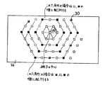
図16に電極30が駆動用半導体素子14の一面全面に形成されている図を示す。
端子配列の理想としては、駆動用半導体素子の中心から、少しずつ外側に配置する。端子の配置は、最外郭までの距離を理想的に減らすために、図のように端子を正3角形をいくつも並べた配置、即ち正6角形状にで配置する。この時端子間がそれぞれ60°の角度を持つように配置すると最も高密度な配置を達成できる。
【0055】
端子を配列する順番は先ず半導体素子の一面の中心部に最初の端子を配置し、この端子を囲むように順に端子を配置する。端子数に合せ、端子数=1+3n(n+1)、(n=1,2,3…)となるように配置する。端子の配列は1、6n(n=1,2,3…)となる。さらに細かく示すと、1、6、12(6,6) 、18(12,6)、24(6,12,6)、30(12,12,6) 、36(6,12,12,6)の規則によって端子を配列する。
【0056】
こうすることで配線端子は中心から六角形が広がるように増えていくが、各端子はできるだけ中心から近い順に配列することが必要である。つまり最外郭の六角形に端子を配置するときに、その六角形の各辺の中点に近いところから順に端子を配置し、最後に各頂点に端子を配置するようにすることが特徴である。
【0057】
図3に示したように半導体素子が細長い場合には、上述のように端子を配列すると配置の途上で半導体素子外になる。そのような場合はもちろん、上述の規則を適宜応用して配置をする。
【0058】
駆動用半導体素子とそれを接続する基板の熱膨張係数が異なるときには、使用環境下での温度変化によって、それぞれが熱収縮を繰り返す。この時半導体素子と基板の接続部(一般には突起状電極または突起電極と封止樹脂)では、熱歪みによって、それらの接続界面あるいは突起電極内部で亀裂が生じる。上記のように端子部を配列することによって、熱歪みを少なくすることができ、接続不良の問題を低減することが可能となる。
【0059】
表示装置は画素の高精細化、画素数の増加が進んでいる。例えば液晶表示装置の場合10”XGA(画素数1024×3×768)では、信号線の画素ピッチは66μmとなっている。さらに、PDA(パーソナルデータアシスタンス)やハイビジョン対応の表示装置では40μm以下の微細な画素ピッチ、数百万の画素数になっている。それに伴い、駆動用半導体素子は多出力になる。XGAを駆動する512出力の駆動用半導体素子では周囲1列配置では端子ピッチが20μm以下になり、接続信頼性が著しく乏しい。
端子の配置を上述の如くエリア状に配置することで、端子ピッチを広くとることができ、接続信頼性を増すことができる。
【0060】
【発明の効果】
以上説明したように本発明は、表示装置の表示部に駆動用半導体素子の長辺が平行になるようにフェイスダウンで実装することで、長辺方向の端子の配置に自由度が増し、設計の容易化を図ることが可能となる。また額縁サイズを最小限にすることを可能とする。
【図面の簡単な説明】
【図1】本発明の実施例に係る表示装置の概念図
【図2】本発明の実施例に係る表示装置の概念図
【図3】本発明の実施例に係る表示装置の額縁部の拡大図
【図4】本発明の実施例に係る表示装置の額縁部の拡大図
【図5】本発明の実施例に係る表示装置の額縁部の拡大図
【図6】本発明の実施例に係る表示装置の額縁部の拡大図
【図7】本発明の実施例に係る表示装置の額縁部の拡大図
【図8】本発明の実施例に係る表示装置の額縁部の拡大図
【図9】本発明の実施例に係る表示装置の額縁部の拡大図
【図10】本発明の実施例に係る表示装置の斜視図
【図11】本発明の実施例に係る表示装置の駆動用半導体素子の断面図
【図12】本発明の実施例に係る表示装置の額縁部の拡大図
【図13】本発明の実施例に係る表示装置の外部配線と接続するためのフレキシブル配線の斜視図
【図14】本発明の実施例に係る表示装置の額縁部の拡大図
【図15】本発明の実施例に係る表示装置の駆動用半導体素子の断面図
【図16】駆動用半導体素子の端子の配列状態を示す図
【図17】従来の表示装置の平面図
【図18】従来の表示装置の額縁部の拡大図
【符号の説明】
11…基板
12…表示画面
14…駆動用半導体素子
15…駆動用半導体素子
16…フレキシブル基板
18…フレキシブル基板
20…フレーム
21…フレーム
22…入力配線
23…出力配線
24…入力端子
25…出力端子
26…検査用端子
27…ショートリング
28…配線
29…ダミーパッド
30…バンプ
31…異方性導電接着剤
32…チップ部品[0001]
[Industrial applications]
The present invention relates to a display device in which a display portion and a driving semiconductor element for driving the display portion are formed on a substrate at the same time, and more particularly to a display device characterized by a method of taking out wiring of the driving semiconductor device.
[0002]
[Prior art]
In a display device, such as a liquid crystal display device or a plasma display device, in which pixels are divided into a matrix and each pixel is driven in a time series by a driving semiconductor element, the driving semiconductor elements are arranged at a fine pitch with a higher definition of pixels. The connection method for connecting to the wiring has become a problem.
[0003]
As a technique corresponding to fine pitch connection, a method called COG (Chip on glass) or COF (Chip on film) for mounting a driving semiconductor element face down on a wiring formed on a substrate has been developed. I have.
[0004]
FIG. 17 shows a schematic view of a display device using a conventional COG mounting in which a driving semiconductor element is mounted on a glass substrate.
A
[0005]
FIG. 18 is an enlarged view of a portion where the
The
[0006]
In such a mounting method, the input terminal occupies the side of the driving semiconductor element on the side opposite to the
[0007]
[Problems to be solved by the invention]
As described above, the conventional method of mounting the driving semiconductor element in the display device has a problem that the frame area of the display device is large.
The present invention has been made in view of the above problems, and an object of the present invention is to provide a display device having a small frame area.
[0008]
Another object of the present invention is to provide a high-definition display device having a very fine wiring pitch.
Still another object of the present invention is to provide a display device in which the degree of freedom in designing a wiring for mounting a driving semiconductor element is greatly improved.
[0009]
[Means for Solving the Problems]
In order to solve the above-described problems, the present invention provides a substrate, a display unit provided on the substrate, a driving semiconductor element disposed around the display unit on the substrate, and a driving semiconductor device. An output wiring for transmitting an output signal from an element to the display unit; and an input wiring for transmitting an input signal for driving the driving semiconductor element, wherein the driving semiconductor elements are respectively opposed to each other. A first output terminal disposed on one long side, a second output terminal disposed on the other long side, and the driving semiconductor element. An input terminal comprising a plurality of terminals provided on the short side of and electrically connected to the input wiring, wherein the output wiring has the first output terminal and the second output terminal. To provide a display device characterized by being alternately connected to
At this time, it is preferable that the first output terminal and the second output terminal are arranged in a staggered manner.
Further, at this time, a plurality of the driving semiconductor elements are provided, and the driving semiconductor elements are arranged so that a long side of each of the driving semiconductor elements faces the display unit, and the input terminal of the adjacent driving semiconductor elements is provided. Are preferably connected to each other by the input wiring, and the signal and the power input to one of the plurality of driving semiconductor elements are sequentially input to the adjacent driving semiconductor element via the input wiring. .
[0015]
In this way, the long side opposite to the display unit is released from the input wiring for driving the driving semiconductor element, thereby making it possible to remove the frame part conventionally required for this part. Thus, the size of the frame can be reduced.
[0016]
At this time, by providing an output terminal for driving the display section on the long side opposite to the display section, connection to finer pitch wiring can be obtained with sufficient reliability. At this time, by providing the output terminals evenly on the two long sides, when the driving semiconductor elements are collectively connected by bumps, a load is evenly applied to each bump, so that connection reliability can be improved.
[0018]
[Action]
As described above, according to the present invention, the input terminal is provided on the short side of the driving semiconductor element, and the long side opposite to the display unit is released from the input terminal, so that the frame part can be significantly reduced. Become. In addition, the degree of freedom in wiring is greatly improved, such as providing an inspection terminal on the long side opposite to the display unit.
[0019]
【Example】
Hereinafter, embodiments of the present invention will be described in detail with reference to the drawings. It should be noted that the following examples are provided to facilitate understanding of the present invention, and the present invention is not limited to these, and can be implemented with various modifications within the scope of the gist.
[0020]
FIG. 1 is a conceptual diagram of a display device according to an embodiment of the present invention. Here, a liquid crystal display device will be described as an example of the display device.
In the liquid crystal display device according to the present embodiment, a
[0021]
FIG. 3 is an enlarged view of a driving semiconductor element portion of the display device.
The driving
[0022]
As described above, the long side of the driving
[0023]
Each wiring can be formed simultaneously with the step of forming the display portion or in another step. The wiring can be formed by a general thin film process or a plating process.
[0024]
A method of connecting the driving
[0025]
The connection between the
[0026]
FIG. 5 is an enlarged view of each driving
As shown in the figure, the
[0027]
By alternately distributing the output wires to the two long sides and connecting them in a staggered manner, it is possible to increase the area of one output terminal and improve the connection reliability.
[0028]
Further, by uniformly distributing the output terminals to the two long sides, the load distribution at the time of connection of the terminals at the time of collective connection becomes uniform, and the reliability at the time of connection can be further improved. In this case, it is preferable that the input terminals formed on the short sides are arranged evenly like the output terminals. By arranging the terminals as uniformly as possible over the entire periphery of the driving semiconductor element, the load balance at the time of connection can be further uniformed. For uniform arrangement, it is desirable that the combined center of gravity of all the terminals of the driving semiconductor element is substantially the same as the center of gravity of the semiconductor element.
[0029]
When such a staggered connection is made, the shift register in the driving semiconductor element is controlled so that the output signal is alternately distributed to the output lines alternately connected to the two long sides. Display can be performed.
[0030]
FIG. 9 shows an example in which an inspection terminal and a short ring are further provided on the long side opposite to the display portion of the driving semiconductor element in the display device described above.
Each
[0031]
By doing so, it is possible to inspect the driving
[0032]
Next, a display device according to another embodiment of the present invention will be described. In this embodiment, the input terminals of the individual driving semiconductor elements are connected to each other by input wiring, and the same parts as those of the display device shown in the previous embodiment are denoted by the same reference numerals, and detailed description thereof will be omitted. I do.
[0033]
FIG. 2 is a schematic diagram of a display device according to the present embodiment.
A
[0034]
FIG. 4 is an enlarged view of a driving semiconductor element portion of the display device.
The driving
[0035]
FIG. 6 shows an enlarged view of each drive
As shown in the figure, the
[0036]
The
[0037]
As in the present embodiment, an input signal or power supplied from the outside by the
[0038]
By doing so, the number of connection points between the
[0039]
Further, since the number of flexible substrates is minimized, the problem of peeling of the flexible substrate is reduced, and the transfer of the substrate is facilitated.
FIG. 7 shows a modification of the method for connecting the input terminals of the driving semiconductor elements of the display device described above.
[0040]
After the
[0041]
In FIGS. 6 and 7, the interconnection of the driving
[0042]
FIG. 8 shows a modification showing another method of connecting the driving semiconductor elements of the display device described above.
The
[0043]
On the other hand, a
[0044]
The connection method of the flexible substrate will be specifically described with reference to FIGS.
FIG. 10 is a schematic diagram of a display device according to the present invention, in which a
[0045]
As shown in FIGS. 12 and 14, the
[0046]
FIG. 11 is an enlarged view of a portion cut along A-A 'in FIG.
The driving
[0047]
FIG. 13 is an enlarged view of a portion indicated by C in FIG.
By mounting the
[0048]
In FIG. 11, the
[0049]
Next, another embodiment of the present invention will be described. In this embodiment, a liquid crystal display device of 10 ″ XGA (1024 × 3 × 768 pixels) was prepared. Further, since a vertical stripe color filter was employed, the number of pixels of the signal line was 3072. The size of the signal line side was Since it is 8 ″, the pixel pitch of the signal line is 66 μm. A driving semiconductor element having 512 outputs was used for driving the display. The size of the semiconductor element is 17 mm × 2.3 mm.
[0050]
In this embodiment, a driving semiconductor element was connected as shown in FIG. As shown in FIG. 8, when the
[0051]
In this embodiment, since the connection method shown in FIG. 5 was adopted, the
[0052]
When the driving semiconductor elements are arranged in 64 × 8 rows, the terminals are also formed on the internal elements. The connection between the driving semiconductor element and the glass substrate was made by forming a gold bump on the terminal of the driving semiconductor element, forming an indium alloy bump on the gold bump, and pressing the glass substrate into pressure. The wiring on the glass substrate uses ITO and contributes to the connection by ITO and antimony in the indium alloy bump.
[0053]
Considering a case where a display device with higher definition will be realized in the future and the number of connection terminals of the driving semiconductor element will increase, it is necessary to form terminals on the entire surface of the driving semiconductor element. Therefore, a method for arranging the terminals of the driving semiconductor element over the entire surface will be described below.
[0054]
FIG. 16 shows a diagram in which the
Ideally, the terminal arrangement is arranged slightly outside the center of the driving semiconductor element. In order to ideally reduce the distance to the outermost terminal, the terminals are arranged in a form in which a number of regular triangles are arranged as shown in the figure, that is, in a regular hexagonal shape. At this time, if the terminals are arranged so as to have an angle of 60 °, the highest density arrangement can be achieved.
[0055]
In order to arrange the terminals, first, the first terminal is arranged at the center of one surface of the semiconductor element, and the terminals are arranged so as to surround this terminal. According to the number of terminals, the terminals are arranged so that the number of terminals = 1 + 3n (n + 1), (n = 1, 2, 3,...). The arrangement of the terminals is 1, 6n (n = 1, 2, 3,...). More specifically, 1, 6, 12 (6, 6), 18 (12, 6), 24 (6, 12, 6), 30 (12, 12, 6), 36 (6, 12, 12, 6) The terminals are arranged according to the rule of ()).
[0056]
By doing so, the number of wiring terminals increases as the hexagon spreads from the center, but it is necessary to arrange the terminals in ascending order from the center as much as possible. In other words, when arranging the terminals in the outermost hexagon, the terminals are arranged in order from a point near the midpoint of each side of the hexagon, and finally, the terminals are arranged at each vertex. .
[0057]
In the case where the semiconductor element is elongated as shown in FIG. 3, when the terminals are arranged as described above, the terminals become outside the semiconductor element in the middle of the arrangement. In such a case, as a matter of course, the arrangement is performed by appropriately applying the above rules.
[0058]
When the driving semiconductor element and the substrate connecting the driving semiconductor element have different coefficients of thermal expansion, each of them repeatedly undergoes thermal contraction due to a temperature change in a use environment. At this time, cracks are generated at the connection interface between the semiconductor element and the substrate (generally, the protruding electrode or the protruding electrode and the sealing resin) at the connection interface thereof or inside the protruding electrode due to thermal strain. By arranging the terminals as described above, thermal distortion can be reduced, and the problem of poor connection can be reduced.
[0059]
In display devices, the definition of pixels and the number of pixels are increasing. For example, in the case of a liquid crystal display device, in 10 ″ XGA (1024 × 3 × 768 pixels), the pixel pitch of the signal line is 66 μm. In the case of a display device compatible with a PDA (personal data assistance) or a high-definition television, it is 40 μm or less. With the fine pixel pitch and the number of millions of pixels, the driving semiconductor element has many outputs, and the terminal pitch of the driving semiconductor element for driving the XGA is 20. And the connection reliability is extremely poor.
By arranging the terminals in an area as described above, the terminal pitch can be widened and the connection reliability can be increased.
[0060]
【The invention's effect】
As described above, the present invention increases the degree of freedom in the arrangement of terminals in the long side direction by mounting the driving semiconductor element face down on the display portion of the display device so that the long sides thereof are parallel to each other. Can be facilitated. Further, it is possible to minimize the frame size.
[Brief description of the drawings]
FIG. 1 is a conceptual diagram of a display device according to an embodiment of the present invention.
FIG. 2 is a conceptual diagram of a display device according to an embodiment of the present invention.
FIG. 3 is an enlarged view of a frame portion of the display device according to the embodiment of the present invention.
FIG. 4 is an enlarged view of a frame portion of the display device according to the embodiment of the present invention.
FIG. 5 is an enlarged view of a frame portion of the display device according to the embodiment of the present invention.
FIG. 6 is an enlarged view of a frame portion of the display device according to the embodiment of the present invention.
FIG. 7 is an enlarged view of a frame portion of the display device according to the embodiment of the present invention.
FIG. 8 is an enlarged view of a frame portion of the display device according to the embodiment of the present invention.
FIG. 9 is an enlarged view of a frame portion of the display device according to the embodiment of the present invention.
FIG. 10 is a perspective view of a display device according to an embodiment of the present invention.
FIG. 11 is a sectional view of a driving semiconductor element of a display device according to an embodiment of the present invention.
FIG. 12 is an enlarged view of a frame portion of the display device according to the embodiment of the present invention.
FIG. 13 is a perspective view of a flexible wiring for connecting to an external wiring of the display device according to the embodiment of the present invention.
FIG. 14 is an enlarged view of a frame portion of the display device according to the embodiment of the present invention.
FIG. 15 is a sectional view of a driving semiconductor element of a display device according to an embodiment of the present invention.
FIG. 16 is a diagram showing an arrangement state of terminals of a driving semiconductor element.
FIG. 17 is a plan view of a conventional display device.
FIG. 18 is an enlarged view of a frame portion of a conventional display device.
[Explanation of symbols]
11 ... substrate
12 ... Display screen
14 ... Driving semiconductor element
15: Driving semiconductor element
16 Flexible board
18 ... Flexible substrate
20… Frame
21… Frame
22 Input wiring
23 Output wiring
24 input terminals
25 Output terminal
26 ... Inspection terminal
27 ... Short ring
28 ... Wiring
29 ... Dummy pad
30 ... Bump
31 Anisotropic conductive adhesive
32: Chip parts
Claims (3)
前記駆動用半導体素子は、それぞれ対向する2つずつの長辺と短辺を有し、一方の長辺側に配置された第1の出力端子と、他方の長辺側に配置された第2の出力端子と、前記駆動用半導体素子のそれぞれの短辺上に設けられ前記入力配線に電気的に接続される複数の端子からなる入力端子と、を有しており、 The driving semiconductor element has two opposing long sides and two short sides, and a first output terminal arranged on one long side and a second output terminal arranged on the other long side. And an input terminal comprising a plurality of terminals provided on each short side of the driving semiconductor element and electrically connected to the input wiring,
前記出力配線が前記第1の出力端子と前記第2の出力端子とに対して交互に接続されたこと The output wiring is alternately connected to the first output terminal and the second output terminal
を特徴とする表示装置。A display device characterized by the above-mentioned.
Priority Applications (3)
| Application Number | Priority Date | Filing Date | Title |
|---|---|---|---|
| JP05960595A JP3556315B2 (en) | 1995-03-20 | 1995-03-20 | Display device and semiconductor element |
| US08/617,241 US5712493A (en) | 1995-03-20 | 1996-03-18 | Display device having driving circuits at the periphery of a substrate |
| KR1019960007542A KR100240431B1 (en) | 1995-03-20 | 1996-03-20 | Display Apparatus |
Applications Claiming Priority (1)
| Application Number | Priority Date | Filing Date | Title |
|---|---|---|---|
| JP05960595A JP3556315B2 (en) | 1995-03-20 | 1995-03-20 | Display device and semiconductor element |
Publications (2)
| Publication Number | Publication Date |
|---|---|
| JPH08262467A JPH08262467A (en) | 1996-10-11 |
| JP3556315B2 true JP3556315B2 (en) | 2004-08-18 |
Family
ID=13118062
Family Applications (1)
| Application Number | Title | Priority Date | Filing Date |
|---|---|---|---|
| JP05960595A Expired - Fee Related JP3556315B2 (en) | 1995-03-20 | 1995-03-20 | Display device and semiconductor element |
Country Status (3)
| Country | Link |
|---|---|
| US (1) | US5712493A (en) |
| JP (1) | JP3556315B2 (en) |
| KR (1) | KR100240431B1 (en) |
Families Citing this family (61)
| Publication number | Priority date | Publication date | Assignee | Title |
|---|---|---|---|---|
| US7081938B1 (en) * | 1993-12-03 | 2006-07-25 | Semiconductor Energy Laboratory Co., Ltd. | Electro-optical device and method for manufacturing the same |
| JPH09179100A (en) * | 1995-12-27 | 1997-07-11 | Sharp Corp | Liquid crystal display device |
| JP3536571B2 (en) * | 1996-03-27 | 2004-06-14 | セイコーエプソン株式会社 | Driving IC, liquid crystal device and electronic equipment |
| KR19980022278A (en) * | 1996-09-20 | 1998-07-06 | 손욱 | Liquid crystal display and cordless phone equipped with this liquid crystal display |
| KR100260611B1 (en) * | 1997-04-03 | 2000-07-01 | 윤종용 | Lcd panel for reparing lines |
| JP3955376B2 (en) * | 1997-05-13 | 2007-08-08 | セイコーエプソン株式会社 | Liquid crystal display panel and liquid crystal display panel inspection method |
| KR100510439B1 (en) * | 1997-08-20 | 2005-10-21 | 삼성전자주식회사 | Chip on glass package structure of lcd driving chip using dummy projecting pad and packaging method therefor |
| TW505803B (en) * | 1997-10-20 | 2002-10-11 | Citizen Watch Co Ltd | Integrated circuit for driving liquid crystal |
| JPH11160734A (en) * | 1997-11-28 | 1999-06-18 | Semiconductor Energy Lab Co Ltd | Liquid crystal electrooptical device |
| JPH11305254A (en) * | 1998-04-24 | 1999-11-05 | Hitachi Ltd | Liquid crystal display |
| JP2000172193A (en) | 1998-12-08 | 2000-06-23 | Fujitsu Ltd | Matrix display device, method of manufacturing the same, and head for thermocompression connection |
| JP4381498B2 (en) * | 1999-02-16 | 2009-12-09 | エーユー オプトロニクス コーポレイション | Liquid crystal display device with COG structure |
| JP2000259091A (en) * | 1999-03-04 | 2000-09-22 | Casio Comput Co Ltd | Display panel, flexible wiring board, and display device having the same |
| JP2000276068A (en) | 1999-03-26 | 2000-10-06 | Seiko Epson Corp | Display device and electronic equipment |
| EP1039788B1 (en) * | 1999-03-26 | 2006-04-19 | Seiko Epson Corporation | Flexible printed wiring board, electro-optical device, and electronic equipment |
| US6664942B1 (en) * | 2000-04-17 | 2003-12-16 | Samsung Electronics Co., Ltd. | Signal transmission film and a liquid crystal display panel having the same |
| KR100304261B1 (en) * | 1999-04-16 | 2001-09-26 | 윤종용 | Tape Carrier Package, Liquid Crystal Display panel assembly contain the Tape Carrier Package, Liquid Crystal Display device contain the Liquid Crystal panel assembly and method for assembling the same |
| US7339568B2 (en) * | 1999-04-16 | 2008-03-04 | Samsung Electronics Co., Ltd. | Signal transmission film and a liquid crystal display panel having the same |
| JP2000321591A (en) * | 1999-05-14 | 2000-11-24 | Nec Corp | Liquid crystal display device |
| JP2001075501A (en) * | 1999-07-02 | 2001-03-23 | Seiko Instruments Inc | Display device and method for inspection of display device |
| JP5020430B2 (en) * | 1999-09-30 | 2012-09-05 | 京セラディスプレイ株式会社 | Electrode connection structure of liquid crystal display panel |
| US6370003B1 (en) | 1999-11-30 | 2002-04-09 | Welch Allyn Data Collections, Inc. | Electrostatic charge resistant instrument system |
| KR100666317B1 (en) * | 1999-12-15 | 2007-01-09 | 삼성전자주식회사 | A driving signal application point determination module, a liquid crystal display panel assembly and a method of driving the liquid crystal display panel assembly including the same |
| TW527513B (en) * | 2000-03-06 | 2003-04-11 | Hitachi Ltd | Liquid crystal display device and manufacturing method thereof |
| IL135571A0 (en) * | 2000-04-10 | 2001-05-20 | Doron Adler | Minimal invasive surgery imaging system |
| US6692430B2 (en) * | 2000-04-10 | 2004-02-17 | C2Cure Inc. | Intra vascular imaging apparatus |
| JP3892650B2 (en) | 2000-07-25 | 2007-03-14 | 株式会社日立製作所 | Liquid crystal display |
| JPWO2002021199A1 (en) * | 2000-09-08 | 2004-01-15 | シチズン時計株式会社 | Liquid crystal display |
| JP2002131774A (en) * | 2000-10-27 | 2002-05-09 | Kyocera Corp | Liquid crystal display |
| JP2002311849A (en) * | 2001-04-19 | 2002-10-25 | Seiko Epson Corp | Electrode driving device and electronic equipment |
| TW558916B (en) * | 2001-08-13 | 2003-10-21 | Chi Mei Optoelectronics Corp | Flat panel display and the printed circuit board thereof |
| EP1463441A4 (en) * | 2001-12-11 | 2009-01-21 | C2Cure Inc | APPARATUS, METHOD AND SYSTEM FOR INTRAVASCULAR PHOTOGRAPHIC IMAGING |
| WO2003098913A2 (en) * | 2002-05-16 | 2003-11-27 | Cbyond Inc. | Miniature camera head |
| JP4054861B2 (en) * | 2002-08-08 | 2008-03-05 | 三菱電機株式会社 | Display device and manufacturing method of display device |
| KR100900537B1 (en) * | 2002-08-23 | 2009-06-02 | 삼성전자주식회사 | Liquid Crystal Display, Inspection Method and Manufacturing Method Thereof |
| US7956976B1 (en) | 2002-09-10 | 2011-06-07 | Hitachi Displays, Ltd. | Liquid crystal display device |
| JP4006304B2 (en) * | 2002-09-10 | 2007-11-14 | 株式会社 日立ディスプレイズ | Image display device |
| KR20040075377A (en) * | 2003-02-20 | 2004-08-30 | 삼성전자주식회사 | Drive ic and display device having the same |
| JP4004994B2 (en) | 2003-06-05 | 2007-11-07 | 株式会社アドバンスト・ディスプレイ | Display device |
| KR100665184B1 (en) * | 2003-11-26 | 2007-01-04 | 삼성전자주식회사 | A liquid crystal display device comprising a semiconductor chip, a tape carrier package on which the chip is mounted, and the tape carrier package. |
| KR100598032B1 (en) * | 2003-12-03 | 2006-07-07 | 삼성전자주식회사 | Tape wiring board, semiconductor chip package using the same, and display panel assembly using the same |
| KR101022278B1 (en) * | 2003-12-15 | 2011-03-21 | 삼성전자주식회사 | Driving chip and display device having same |
| KR101051013B1 (en) * | 2003-12-16 | 2011-07-21 | 삼성전자주식회사 | Driving chip and display device having same |
| TWI271691B (en) * | 2004-07-07 | 2007-01-21 | Chi Mei Optoelectronics Corp | Liquid crystal panel structure |
| US7300397B2 (en) * | 2004-07-29 | 2007-11-27 | C2C Cure, Inc. | Endoscope electronics assembly |
| US20060164510A1 (en) * | 2005-01-24 | 2006-07-27 | Doron Adler | Sensor with narrow mounting profile |
| US20060221218A1 (en) * | 2005-04-05 | 2006-10-05 | Doron Adler | Image sensor with improved color filter |
| JP4925757B2 (en) * | 2006-07-28 | 2012-05-09 | 京セラ株式会社 | Display panel and display device |
| JP4198736B2 (en) * | 2007-07-26 | 2008-12-17 | 三菱電機株式会社 | Source line driving circuit and display device including the source line driving circuit |
| US20090046171A1 (en) * | 2007-08-16 | 2009-02-19 | C2Cure, Inc. | Non-linear color correction |
| TWI373107B (en) * | 2008-04-24 | 2012-09-21 | Hannstar Display Corp | Chip having a driving integrated circuit and liquid crystal display having the same |
| JP5452290B2 (en) * | 2010-03-05 | 2014-03-26 | ラピスセミコンダクタ株式会社 | Display panel |
| KR101765656B1 (en) * | 2010-12-23 | 2017-08-08 | 삼성디스플레이 주식회사 | Driving Integrated Circuit and Display Apparatus comprising Driving Integrated Circuit |
| JP2013210646A (en) * | 2013-05-08 | 2013-10-10 | Japan Display Inc | Driver |
| US20140354934A1 (en) * | 2013-05-28 | 2014-12-04 | Shenzhen China Star Optoelectronics Technology Co., Ltd | Display device and method for manufacturing the display device |
| JP5526265B2 (en) * | 2013-05-31 | 2014-06-18 | 株式会社ジャパンディスプレイ | Liquid crystal display |
| US9257763B2 (en) | 2013-07-02 | 2016-02-09 | Gyrus Acmi, Inc. | Hybrid interconnect |
| US9510739B2 (en) | 2013-07-12 | 2016-12-06 | Gyrus Acmi, Inc. | Endoscope small imaging system |
| KR20150114632A (en) * | 2014-04-01 | 2015-10-13 | 삼성디스플레이 주식회사 | Touch unit and touch display apparatus including the same |
| CN105807514B (en) * | 2016-04-29 | 2019-02-15 | 武汉天马微电子有限公司 | Display device |
| CN110610657A (en) * | 2018-06-14 | 2019-12-24 | 格科微电子(上海)有限公司 | Design method of driving chip of display panel for portable electronic device |
Family Cites Families (9)
| Publication number | Priority date | Publication date | Assignee | Title |
|---|---|---|---|---|
| JPS5840728B2 (en) * | 1978-08-23 | 1983-09-07 | 株式会社日立製作所 | liquid crystal display device |
| JP2653099B2 (en) * | 1988-05-17 | 1997-09-10 | セイコーエプソン株式会社 | Active matrix panel, projection display and viewfinder |
| JPH0752265B2 (en) * | 1988-07-07 | 1995-06-05 | 松下電器産業株式会社 | Drive circuit |
| US5452114A (en) * | 1991-09-13 | 1995-09-19 | Canon Kabushiki Kaisha | Ferroelectric liquid crystal device with grooves between electrode on one substrate, ridges on the other |
| JP3254230B2 (en) * | 1991-10-15 | 2002-02-04 | シャープ株式会社 | LCD Display Panel Wiring Structure |
| JP2837027B2 (en) * | 1992-06-17 | 1998-12-14 | シャープ株式会社 | Tape carrier package |
| TW232065B (en) * | 1992-04-16 | 1994-10-11 | Sharp Kk | |
| JPH0611683A (en) * | 1992-06-25 | 1994-01-21 | Seiko Epson Corp | Wiring structure for integrated circuits, electro-optical device, and electronic printing device |
| US5467210A (en) * | 1993-02-16 | 1995-11-14 | Casio Computer Co., Ltd. | Arrangement of bonding IC chip to liquid crystal display device |
-
1995
- 1995-03-20 JP JP05960595A patent/JP3556315B2/en not_active Expired - Fee Related
-
1996
- 1996-03-18 US US08/617,241 patent/US5712493A/en not_active Expired - Lifetime
- 1996-03-20 KR KR1019960007542A patent/KR100240431B1/en not_active Expired - Fee Related
Also Published As
| Publication number | Publication date |
|---|---|
| US5712493A (en) | 1998-01-27 |
| KR960035091A (en) | 1996-10-24 |
| JPH08262467A (en) | 1996-10-11 |
| KR100240431B1 (en) | 2000-01-15 |
Similar Documents
| Publication | Publication Date | Title |
|---|---|---|
| JP3556315B2 (en) | Display device and semiconductor element | |
| TWI610281B (en) | Display panel | |
| US5585666A (en) | Semiconductor device with chip layout having inner electrode configuration and liquid crystal display apparatus employing the semiconductor device | |
| JP3549760B2 (en) | Flat panel display | |
| JPWO1991016656A1 (en) | Semiconductor device and data input/output device with circuit cell array | |
| JPH0954333A (en) | Display device and IC chip used for the same | |
| JPH05150263A (en) | Active matrix type liquid crystal display device | |
| JP2007058174A (en) | Array substrate and display device having the same | |
| KR101644055B1 (en) | Borderless liquid crystal display device | |
| CN217641339U (en) | Display panel and display device | |
| JPS59210419A (en) | liquid crystal display device | |
| TWI326373B (en) | Liquid crystal display with cascade design and a circuit pattern thereon | |
| CN100451749C (en) | Liquid crystal display panel and circuit structure thereof | |
| JP3199570B2 (en) | Display device | |
| JP3404446B2 (en) | Tape carrier package and liquid crystal display device provided with the tape carrier package | |
| JP2760846B2 (en) | Liquid crystal display | |
| JP2002246404A (en) | Semiconductor device with bump | |
| JPH04281431A (en) | Liquid crystal display device | |
| KR100824533B1 (en) | Display driving chip | |
| TWI409917B (en) | Chip layout for reducing warpage and method thereof | |
| JPH04304427A (en) | Liquid crystal display device | |
| CN116913176B (en) | Electronic devices | |
| JP2626389B2 (en) | Chip components | |
| JPH06202135A (en) | Liquid crystal display device | |
| JPS58197769A (en) | Semiconductor integrated circuit device |
Legal Events
| Date | Code | Title | Description |
|---|---|---|---|
| A131 | Notification of reasons for refusal |
Free format text: JAPANESE INTERMEDIATE CODE: A131 Effective date: 20040130 |
|
| A521 | Request for written amendment filed |
Free format text: JAPANESE INTERMEDIATE CODE: A523 Effective date: 20040316 |
|
| TRDD | Decision of grant or rejection written | ||
| A01 | Written decision to grant a patent or to grant a registration (utility model) |
Free format text: JAPANESE INTERMEDIATE CODE: A01 Effective date: 20040507 |
|
| A61 | First payment of annual fees (during grant procedure) |
Free format text: JAPANESE INTERMEDIATE CODE: A61 Effective date: 20040512 |
|
| R150 | Certificate of patent or registration of utility model |
Free format text: JAPANESE INTERMEDIATE CODE: R150 |
|
| FPAY | Renewal fee payment (event date is renewal date of database) |
Free format text: PAYMENT UNTIL: 20090521 Year of fee payment: 5 |
|
| FPAY | Renewal fee payment (event date is renewal date of database) |
Free format text: PAYMENT UNTIL: 20090521 Year of fee payment: 5 |
|
| S111 | Request for change of ownership or part of ownership |
Free format text: JAPANESE INTERMEDIATE CODE: R313117 |
|
| FPAY | Renewal fee payment (event date is renewal date of database) |
Free format text: PAYMENT UNTIL: 20090521 Year of fee payment: 5 |
|
| R350 | Written notification of registration of transfer |
Free format text: JAPANESE INTERMEDIATE CODE: R350 |
|
| FPAY | Renewal fee payment (event date is renewal date of database) |
Free format text: PAYMENT UNTIL: 20090521 Year of fee payment: 5 |
|
| FPAY | Renewal fee payment (event date is renewal date of database) |
Free format text: PAYMENT UNTIL: 20100521 Year of fee payment: 6 |
|
| S533 | Written request for registration of change of name |
Free format text: JAPANESE INTERMEDIATE CODE: R313533 |
|
| FPAY | Renewal fee payment (event date is renewal date of database) |
Free format text: PAYMENT UNTIL: 20100521 Year of fee payment: 6 |
|
| R350 | Written notification of registration of transfer |
Free format text: JAPANESE INTERMEDIATE CODE: R350 |
|
| FPAY | Renewal fee payment (event date is renewal date of database) |
Free format text: PAYMENT UNTIL: 20100521 Year of fee payment: 6 |
|
| FPAY | Renewal fee payment (event date is renewal date of database) |
Free format text: PAYMENT UNTIL: 20110521 Year of fee payment: 7 |
|
| FPAY | Renewal fee payment (event date is renewal date of database) |
Free format text: PAYMENT UNTIL: 20110521 Year of fee payment: 7 |
|
| FPAY | Renewal fee payment (event date is renewal date of database) |
Free format text: PAYMENT UNTIL: 20120521 Year of fee payment: 8 |
|
| S531 | Written request for registration of change of domicile |
Free format text: JAPANESE INTERMEDIATE CODE: R313531 |
|
| FPAY | Renewal fee payment (event date is renewal date of database) |
Free format text: PAYMENT UNTIL: 20120521 Year of fee payment: 8 |
|
| R350 | Written notification of registration of transfer |
Free format text: JAPANESE INTERMEDIATE CODE: R350 |
|
| FPAY | Renewal fee payment (event date is renewal date of database) |
Free format text: PAYMENT UNTIL: 20120521 Year of fee payment: 8 |
|
| FPAY | Renewal fee payment (event date is renewal date of database) |
Free format text: PAYMENT UNTIL: 20130521 Year of fee payment: 9 |
|
| S533 | Written request for registration of change of name |
Free format text: JAPANESE INTERMEDIATE CODE: R313533 |
|
| FPAY | Renewal fee payment (event date is renewal date of database) |
Free format text: PAYMENT UNTIL: 20130521 Year of fee payment: 9 |
|
| R350 | Written notification of registration of transfer |
Free format text: JAPANESE INTERMEDIATE CODE: R350 |
|
| FPAY | Renewal fee payment (event date is renewal date of database) |
Free format text: PAYMENT UNTIL: 20140521 Year of fee payment: 10 |
|
| LAPS | Cancellation because of no payment of annual fees |