JP2025068231A - Print circuit board - Google Patents
Print circuit board Download PDFInfo
- Publication number
- JP2025068231A JP2025068231A JP2023177991A JP2023177991A JP2025068231A JP 2025068231 A JP2025068231 A JP 2025068231A JP 2023177991 A JP2023177991 A JP 2023177991A JP 2023177991 A JP2023177991 A JP 2023177991A JP 2025068231 A JP2025068231 A JP 2025068231A
- Authority
- JP
- Japan
- Prior art keywords
- layer
- resin
- conductor
- wiring board
- printed wiring
- Prior art date
- Legal status (The legal status is an assumption and is not a legal conclusion. Google has not performed a legal analysis and makes no representation as to the accuracy of the status listed.)
- Pending
Links
Images


Classifications
-
- H—ELECTRICITY
- H05—ELECTRIC TECHNIQUES NOT OTHERWISE PROVIDED FOR
- H05K—PRINTED CIRCUITS; CASINGS OR CONSTRUCTIONAL DETAILS OF ELECTRIC APPARATUS; MANUFACTURE OF ASSEMBLAGES OF ELECTRICAL COMPONENTS
- H05K1/00—Printed circuits
- H05K1/02—Details
- H05K1/11—Printed elements for providing electric connections to or between printed circuits
-
- H—ELECTRICITY
- H05—ELECTRIC TECHNIQUES NOT OTHERWISE PROVIDED FOR
- H05K—PRINTED CIRCUITS; CASINGS OR CONSTRUCTIONAL DETAILS OF ELECTRIC APPARATUS; MANUFACTURE OF ASSEMBLAGES OF ELECTRICAL COMPONENTS
- H05K3/00—Apparatus or processes for manufacturing printed circuits
- H05K3/40—Forming printed elements for providing electric connections to or between printed circuits
- H05K3/4038—Through-connections; Vertical interconnect access [VIA] connections
- H05K3/4053—Through-connections; Vertical interconnect access [VIA] connections by thick-film techniques
- H05K3/4069—Through-connections; Vertical interconnect access [VIA] connections by thick-film techniques for via connections in organic insulating substrates
-
- H—ELECTRICITY
- H05—ELECTRIC TECHNIQUES NOT OTHERWISE PROVIDED FOR
- H05K—PRINTED CIRCUITS; CASINGS OR CONSTRUCTIONAL DETAILS OF ELECTRIC APPARATUS; MANUFACTURE OF ASSEMBLAGES OF ELECTRICAL COMPONENTS
- H05K1/00—Printed circuits
- H05K1/02—Details
- H05K1/03—Use of materials for the substrate
- H05K1/0313—Organic insulating material
- H05K1/0353—Organic insulating material consisting of two or more materials, e.g. two or more polymers, polymer + filler, + reinforcement
- H05K1/0373—Organic insulating material consisting of two or more materials, e.g. two or more polymers, polymer + filler, + reinforcement containing additives, e.g. fillers
-
- H—ELECTRICITY
- H05—ELECTRIC TECHNIQUES NOT OTHERWISE PROVIDED FOR
- H05K—PRINTED CIRCUITS; CASINGS OR CONSTRUCTIONAL DETAILS OF ELECTRIC APPARATUS; MANUFACTURE OF ASSEMBLAGES OF ELECTRICAL COMPONENTS
- H05K1/00—Printed circuits
- H05K1/02—Details
- H05K1/03—Use of materials for the substrate
- H05K1/05—Insulated conductive substrates, e.g. insulated metal substrate
- H05K1/056—Insulated conductive substrates, e.g. insulated metal substrate the metal substrate being covered by an organic insulating layer
-
- H—ELECTRICITY
- H05—ELECTRIC TECHNIQUES NOT OTHERWISE PROVIDED FOR
- H05K—PRINTED CIRCUITS; CASINGS OR CONSTRUCTIONAL DETAILS OF ELECTRIC APPARATUS; MANUFACTURE OF ASSEMBLAGES OF ELECTRICAL COMPONENTS
- H05K1/00—Printed circuits
- H05K1/02—Details
- H05K1/11—Printed elements for providing electric connections to or between printed circuits
- H05K1/115—Via connections; Lands around holes or via connections
- H05K1/116—Lands, clearance holes or other lay-out details concerning the surrounding of a via
-
- H—ELECTRICITY
- H05—ELECTRIC TECHNIQUES NOT OTHERWISE PROVIDED FOR
- H05K—PRINTED CIRCUITS; CASINGS OR CONSTRUCTIONAL DETAILS OF ELECTRIC APPARATUS; MANUFACTURE OF ASSEMBLAGES OF ELECTRICAL COMPONENTS
- H05K3/00—Apparatus or processes for manufacturing printed circuits
- H05K3/0011—Working of insulating substrates or insulating layers
- H05K3/0017—Etching of the substrate by chemical or physical means
- H05K3/0026—Etching of the substrate by chemical or physical means by laser ablation
- H05K3/0032—Etching of the substrate by chemical or physical means by laser ablation of organic insulating material
- H05K3/0035—Etching of the substrate by chemical or physical means by laser ablation of organic insulating material of blind holes, i.e. having a metal layer at the bottom
-
- H—ELECTRICITY
- H05—ELECTRIC TECHNIQUES NOT OTHERWISE PROVIDED FOR
- H05K—PRINTED CIRCUITS; CASINGS OR CONSTRUCTIONAL DETAILS OF ELECTRIC APPARATUS; MANUFACTURE OF ASSEMBLAGES OF ELECTRICAL COMPONENTS
- H05K3/00—Apparatus or processes for manufacturing printed circuits
- H05K3/38—Improvement of the adhesion between the insulating substrate and the metal
- H05K3/386—Improvement of the adhesion between the insulating substrate and the metal by the use of an organic polymeric bonding layer, e.g. adhesive
-
- H—ELECTRICITY
- H05—ELECTRIC TECHNIQUES NOT OTHERWISE PROVIDED FOR
- H05K—PRINTED CIRCUITS; CASINGS OR CONSTRUCTIONAL DETAILS OF ELECTRIC APPARATUS; MANUFACTURE OF ASSEMBLAGES OF ELECTRICAL COMPONENTS
- H05K3/00—Apparatus or processes for manufacturing printed circuits
- H05K3/46—Manufacturing multilayer circuits
- H05K3/4611—Manufacturing multilayer circuits by laminating two or more circuit boards
- H05K3/4626—Manufacturing multilayer circuits by laminating two or more circuit boards characterised by the insulating layers or materials
-
- H—ELECTRICITY
- H05—ELECTRIC TECHNIQUES NOT OTHERWISE PROVIDED FOR
- H05K—PRINTED CIRCUITS; CASINGS OR CONSTRUCTIONAL DETAILS OF ELECTRIC APPARATUS; MANUFACTURE OF ASSEMBLAGES OF ELECTRICAL COMPONENTS
- H05K2201/00—Indexing scheme relating to printed circuits covered by H05K1/00
- H05K2201/02—Fillers; Particles; Fibers; Reinforcement materials
- H05K2201/0203—Fillers and particles
- H05K2201/0206—Materials
- H05K2201/0209—Inorganic, non-metallic particles
-
- H—ELECTRICITY
- H05—ELECTRIC TECHNIQUES NOT OTHERWISE PROVIDED FOR
- H05K—PRINTED CIRCUITS; CASINGS OR CONSTRUCTIONAL DETAILS OF ELECTRIC APPARATUS; MANUFACTURE OF ASSEMBLAGES OF ELECTRICAL COMPONENTS
- H05K2201/00—Indexing scheme relating to printed circuits covered by H05K1/00
- H05K2201/03—Conductive materials
- H05K2201/0332—Structure of the conductor
- H05K2201/0388—Other aspects of conductors
-
- H—ELECTRICITY
- H05—ELECTRIC TECHNIQUES NOT OTHERWISE PROVIDED FOR
- H05K—PRINTED CIRCUITS; CASINGS OR CONSTRUCTIONAL DETAILS OF ELECTRIC APPARATUS; MANUFACTURE OF ASSEMBLAGES OF ELECTRICAL COMPONENTS
- H05K2201/00—Indexing scheme relating to printed circuits covered by H05K1/00
- H05K2201/09—Shape and layout
- H05K2201/09209—Shape and layout details of conductors
- H05K2201/095—Conductive through-holes or vias
- H05K2201/09509—Blind vias, i.e. vias having one side closed
-
- H—ELECTRICITY
- H05—ELECTRIC TECHNIQUES NOT OTHERWISE PROVIDED FOR
- H05K—PRINTED CIRCUITS; CASINGS OR CONSTRUCTIONAL DETAILS OF ELECTRIC APPARATUS; MANUFACTURE OF ASSEMBLAGES OF ELECTRICAL COMPONENTS
- H05K2201/00—Indexing scheme relating to printed circuits covered by H05K1/00
- H05K2201/09—Shape and layout
- H05K2201/09209—Shape and layout details of conductors
- H05K2201/095—Conductive through-holes or vias
- H05K2201/09554—Via connected to metal substrate
-
- H—ELECTRICITY
- H05—ELECTRIC TECHNIQUES NOT OTHERWISE PROVIDED FOR
- H05K—PRINTED CIRCUITS; CASINGS OR CONSTRUCTIONAL DETAILS OF ELECTRIC APPARATUS; MANUFACTURE OF ASSEMBLAGES OF ELECTRICAL COMPONENTS
- H05K3/00—Apparatus or processes for manufacturing printed circuits
- H05K3/02—Apparatus or processes for manufacturing printed circuits in which the conductive material is applied to the surface of the insulating support and is thereafter removed from such areas of the surface which are not intended for current conducting or shielding
- H05K3/06—Apparatus or processes for manufacturing printed circuits in which the conductive material is applied to the surface of the insulating support and is thereafter removed from such areas of the surface which are not intended for current conducting or shielding the conductive material being removed chemically or electrolytically, e.g. by photo-etch process
- H05K3/07—Apparatus or processes for manufacturing printed circuits in which the conductive material is applied to the surface of the insulating support and is thereafter removed from such areas of the surface which are not intended for current conducting or shielding the conductive material being removed chemically or electrolytically, e.g. by photo-etch process being removed electrolytically
Landscapes
- Engineering & Computer Science (AREA)
- Microelectronics & Electronic Packaging (AREA)
- Manufacturing & Machinery (AREA)
- Physics & Mathematics (AREA)
- Optics & Photonics (AREA)
- Production Of Multi-Layered Print Wiring Board (AREA)
- Manufacturing Of Printed Wiring (AREA)
Abstract
Description
本明細書によって開示される技術はプリント配線板に関する。 The technology disclosed in this specification relates to printed wiring boards.
特許文献1は、基板上に導体回路と層間樹脂絶縁層を順次積層することと、導体回路の表面の少なくとも一部に、トリアジン化合物を含む層を形成することを含む多層プリント配線板の製造方法を開示する。導体回路と層間樹脂絶縁層はトリアジン化合物を含む層を介して接着される。 Patent Document 1 discloses a method for manufacturing a multilayer printed wiring board, which includes sequentially laminating a conductor circuit and an interlayer resin insulating layer on a substrate, and forming a layer containing a triazine compound on at least a portion of the surface of the conductor circuit. The conductor circuit and the interlayer resin insulating layer are bonded via the layer containing a triazine compound.
[特許文献1の課題]
特許文献1の技術を用いて製造されるプリント配線板では、導体回路と層間樹脂絶縁層の間に大きいストレスが働くと、導体回路と層間樹脂絶縁層の間に剥がれが発生すると予測される。例えば、ビルドアップ層内の導体層の数が5以上であると、導体回路と層間樹脂絶縁層との間に働くストレスは増えると考えられる。ビルドアップ層内の導体層の数が5以上であると、導体回路と層間樹脂絶縁層の間に剥がれが発生すると予測される。例えば、プリント配線板の各辺の長さが50mmを超えると、導体回路と層間樹脂絶縁層の間に剥がれが発生すると予測される。
[Problems of Patent Document 1]
In a printed wiring board manufactured using the technology of Patent Document 1, when a large stress acts between the conductor circuit and the interlayer resin insulation layer, peeling is predicted to occur between the conductor circuit and the interlayer resin insulation layer. For example, when the number of conductor layers in the build-up layer is 5 or more, it is considered that the stress acting between the conductor circuit and the interlayer resin insulation layer increases. When the number of conductor layers in the build-up layer is 5 or more, peeling is predicted to occur between the conductor circuit and the interlayer resin insulation layer. For example, when the length of each side of the printed wiring board exceeds 50 mm, peeling is predicted to occur between the conductor circuit and the interlayer resin insulation layer.
本発明のプリント配線板は、絶縁層と、前記絶縁層上に形成される導体層と、前記導体層上に形成されていて、有機製の材料からなる接着層と、前記絶縁層と前記導体層上に形成されている樹脂絶縁層、とを有する。前記樹脂絶縁層は樹脂と前記樹脂内に分散されている無機粒子を有している。前記導体層の表面は略平滑である。前記接着層は、平滑膜と前記平滑膜から突出する突出部で形成されている。前記突出部は複数の突起で形成されている。前記複数の突起間のスペースは前記樹脂絶縁層で充填されている。所定面積当たりの前記スペース内の前記無機粒子の数(B1)は前記所定面積当たりの前記スペース外の前記無機粒子の数(B2)より小さい。 The printed wiring board of the present invention has an insulating layer, a conductor layer formed on the insulating layer, an adhesive layer formed on the conductor layer and made of an organic material, and a resin insulating layer formed on the insulating layer and the conductor layer. The resin insulating layer has resin and inorganic particles dispersed in the resin. The surface of the conductor layer is approximately smooth. The adhesive layer is formed of a smooth film and a protruding portion protruding from the smooth film. The protruding portion is formed of a plurality of protrusions. The space between the plurality of protrusions is filled with the resin insulating layer. The number of the inorganic particles within the space per given area (B1) is smaller than the number of the inorganic particles outside the space per given area (B2).
本発明の実施形態のプリント配線板は、導体層と樹脂絶縁層で挟まれる接着層を有する。接着層は導体層と樹脂絶縁層を接着している。接着層はほぼ平滑な平滑膜と平滑膜から突出している突出部で形成されている。接着層が突出部と平滑膜によって形成される凹凸を有する。突出部は複数の突起によって形成される凹凸を有する。そのため導体層と樹脂絶縁層が接着層を介して十分に密着する。接着層の熱膨張率(CTE)と樹脂絶縁層のCTEは異なる。プリント配線板が熱衝撃を受けると、接着層の突起間のスペースを充填する樹脂絶縁層の変形量と接着層の変形量は異なる。とくにスペースを充填する樹脂絶縁層が無機粒子を含むと両者の変形量の差が大きい。両者の変形量の差が大きいと突起が破壊され易い。実施形態のプリント配線板では、所定面積当たりのスペース内の無機粒子の数(B1)が所定面積当たりのスペース外の無機粒子の数(B2)より小さい。スペースを充填する樹脂絶縁層の変形量と接着層の変形量の差が小さい。突起が破壊されがたい。樹脂絶縁層が導体層から剥がれがたい。高い品質を有するプリント配線板が提供される。 The printed wiring board of the embodiment of the present invention has an adhesive layer sandwiched between the conductor layer and the resin insulating layer. The adhesive layer bonds the conductor layer and the resin insulating layer. The adhesive layer is formed of a nearly smooth film and a protruding portion protruding from the smooth film. The adhesive layer has unevenness formed by the protruding portion and the smooth film. The protruding portion has unevenness formed by a plurality of protrusions. Therefore, the conductor layer and the resin insulating layer are sufficiently adhered to each other via the adhesive layer. The coefficient of thermal expansion (CTE) of the adhesive layer is different from the CTE of the resin insulating layer. When the printed wiring board is subjected to thermal shock, the deformation amount of the resin insulating layer filling the space between the protrusions of the adhesive layer and the deformation amount of the adhesive layer are different. In particular, when the resin insulating layer filling the space contains inorganic particles, the difference in the deformation amount between the two is large. If the difference in the deformation amount between the two is large, the protrusions are easily destroyed. In the printed wiring board of the embodiment, the number of inorganic particles in the space per specified area (B1) is smaller than the number of inorganic particles outside the space per specified area (B2). The difference in the deformation amount between the resin insulating layer filling the space and the adhesive layer is small. The protrusions are less likely to break. The resin insulating layer is less likely to peel off from the conductor layer. This provides a high-quality printed wiring board.
[実施形態]
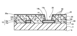
図1は実施形態のプリント配線板2を示す断面図である。図1に示されるように、プリント配線板2は絶縁層4と第1導体層10と樹脂絶縁層20と第2導体層30とビア導体40を有する。第1導体層10は導体層の一例である。ビア導体40は樹脂絶縁層20に形成されている開口26内に形成されている。プリント配線板2は第1導体層10上に接着層100を有する。接着層100は第1導体層10と樹脂絶縁層20で挟まれている。第1導体層10と第2導体層30は隣接している。第1導体層10と第2導体層30の間に導体層は存在しない。
[Embodiment]
FIG. 1 is a cross-sectional view showing a printed
絶縁層4は熱硬化性樹脂を用いて形成される。絶縁層4は光硬化性樹脂でも良い。絶縁層4はシリカ等の無機粒子を含んでもよい。絶縁層4はガラスクロス等の補強材を含んでもよい。絶縁層4は第3面6と第3面6と反対側の第4面8を有する。
The
第1導体層10は絶縁層4の第3面6上に形成されている。第1導体層10は信号配線12とパッド14を含む。図に示されていないが、第1導体層10は信号配線12とパッド14以外の導体回路も含んでいる。第1導体層10は主に銅によって形成される。第1導体層10は、絶縁層4上のシード層10aとシード層10a上の電解めっき層10bで形成されている。第1導体層10の表面(上面と側面)は平滑である。第1導体層10の表面の粗さは二乗平均平方根粗さ(Rq)で示される。第1導体層10の表面のRqは0.23μm以下である。第1導体層10の表面のRqは0.18μm以下であることが好ましい。第1導体層10の表面のRqは0.1μm以下であることがより好ましい。
The
パッド14の表面は第1表面14aと第2表面14bで形成される。第1表面14aは樹脂絶縁層20に形成されている開口26から露出している。第2表面14bは第1表面14a以外の表面である。第2表面14bの二乗平均平方根粗さ(Rq)は0.23μm以下である。第1表面14aは接着層100で覆われていない。第2表面14bは接着層100で覆われている。信号配線12の表面(上面と側面)は接着層100で覆われている。第1導体層10の側面は接着層100で覆われている。
The surface of the
接着層100は樹脂で形成されている。接着層100は有機製の材料(有機製樹脂)で形成されている。接着層100は無機粒子を含んでいない。あるいは、接着層100はシリカ等の無機粒子を含む。接着層100が無機粒子を含む場合、無機粒子の直径は数nmである。有機製の材料は窒素系有機化合物である。窒素系有機化合物は例えばテトラゾール化合物である。窒素系有機化合物の例は特開2015-54987号公報に開示されている。接着層100は第1導体層10から露出する第3面6を覆っていない。接着層100は第1導体層10と樹脂絶縁層20で挟まれている。接着層100は第1導体層10と樹脂絶縁層20を接着している。
The
図2はパッド14の第2表面14b上に形成されている接着層100の一部を示す拡大断面図である。図2に示されるように、接着層100はほぼ平滑な平滑膜110と平滑膜110から突出している複数の突出部120で形成されている。パッド14の側面に形成されている接着層100は、図2に示されている接着層100と同様な平滑膜110と複数の突出部120で形成されている。形状も同様である。信号配線12の上面と側面に形成されている接着層100は、図2と同様な平滑膜110と複数の突出部120で形成されている。形状も同様である。
Figure 2 is an enlarged cross-sectional view showing a portion of the
平滑膜110はほぼ均一な厚みTを有する。平滑膜110の厚みTは10nm以上、120nm以下である。突出部120から露出する平滑膜110の面積(S1)と接着層100の面積(S2)との比(S1/S2)は0.1以上、0.5以下である。第1導体層10の上面上の平滑膜110は第1導体層10の上面の形状にほぼ沿って形成されている。第1導体層10の第2表面14b上の平滑膜110は第1導体層10の第2表面14bの形状にほぼ沿って形成されている。第1導体層10の側面上の平滑膜110は第1導体層10の側面の形状にほぼ沿って形成されている。第1導体層10の上面と側面にうねりが形成されている場合、平滑膜110はそのうねりに追随している。
The smoothing
突出部120は複数の突起122で形成されている。複数の突起122により、突出部120の上面に凹凸が形成される。1mm2あたりの突起122の数は5以上、15以下である。突出部120は、平滑膜110の上面と突出部120の頂部間に高さH1、H2を有する。高さH1、H2の最大値は、平滑膜110の厚みTの10倍以上、30倍以下である。高さH1、H2は、200nm以上、450nm以下である。
The protruding
樹脂絶縁層20は、接着層100を介して第1導体層10上に形成されている。樹脂絶縁層20は接着層100によって第1導体層10と接着している。樹脂絶縁層20は第1面22と第1面22と反対側の第2面24を有する。樹脂絶縁層20の第2面24は第1導体層10と対向する。第2面24は接着層100に接している。樹脂絶縁層20はパッド14を露出する開口26を有している。樹脂絶縁層20の第1面22は凹凸を有していない。第1面22は荒らされていない。第1面22は平滑に形成されている。樹脂絶縁層20の厚さは、第2導体層30の厚さの2倍以上である。樹脂絶縁層20の厚さは第1面22と第1導体層10の上面の間の距離である。
The
樹脂絶縁層20は樹脂80と樹脂80内に分散されている多数の無機粒子90を有している。樹脂絶縁層20は樹脂80と樹脂80内に分散されている多数の無機粒子90で形成されている。樹脂80はエポキシ系樹脂である。樹脂の例は熱硬化性樹脂と光硬化性樹脂である。無機粒子90は、例えば、シリカやアルミナである。樹脂絶縁層20中の無機粒子90の量は70wt%以上である。
The
図2に示されるように、接着層100の突出部120を形成する複数の突起122間にスペース130が存在する。スペース130の数は複数である。各スペース130は樹脂絶縁層20で充填されている。各スペース130内の樹脂絶縁層20は樹脂絶縁層20に由来する樹脂80を必ず含む。各スペース130内の樹脂絶縁層20は樹脂絶縁層20に由来する無機粒子90を含む、または、含まない。所定面積当たりのスペース130内の無機粒子90の数(B1)は所定面積当たりのスペース130外の無機粒子90の数(B2)より小さい。数B1と数B2の比(数B1/数B2)は0.5より小さい。比(数B1/数B2)は0.1より小さくてもよい。比(数B1/数B2)は0であってもよい。比が0の場合、比(数B1/数B2)は比0と表記される。比0に相当するスペース130内の樹脂絶縁層20はスペース130内に無機粒子90を含まない。数B1と数B2の計測はプリント配線板2の断面を用いて行われる。計測に用いられる断面は第1面22に垂直な面でプリント配線板2を切断することで得られる。所定面積の例は4μm2以上、25μm2以下である。計測箇所の数は複数であることが好ましい。各計測場所は異なる。計測箇所の数の例は5以上、30以下である。数B1と数B2は各計測場所の無機粒子90の数の平均値である。
As shown in FIG. 2, there are
複数のスペース130内の樹脂絶縁層20が観察されると、各スペース130は第1スペース131と第2スペース132に分類される。第1スペース131は樹脂80のみで充填されている。第2スペース132は無機粒子90と樹脂80で充填されている。第1スペース131の数(N1)とスペース130の総数(N2)の比(N1/N2)は0.5以上である。半分以上のスペース130が無機粒子90を含まない。比(N1/N2)は0.7以上であることが好ましい。比(N1/N2)は0.85以上であることがより好ましい。比(N1/N2)は1であってもよい。比(N1/N2)の算出に用いられるスペース130の総数(N2)は10以上であることが好ましい。総数(N2)は第1スペース131の数と第2スペース132の数の和である。総数(N2)は測定箇所の数で代表されても良い。例えば、10個のスペース130が無機粒子の有無について評価されると、総数(N2)は10である。
When the
図1に示されるように、第2導体層30は樹脂絶縁層20の第1面22上に形成されている。第2導体層30は第1信号配線32と第2信号配線34とランド36とを含む。図に示されていないが、第2導体層30は第1信号配線32と第2信号配線34とランド36以外の導体回路も含んでいる。第1信号配線32と第2信号配線34はペア配線を形成している。第2導体層30は主に銅によって形成される。第2導体層30は、第1面22上のシード層30aとシード層30a上の電解めっき層30bで形成されている。
As shown in FIG. 1, the
ビア導体40は開口26内に形成されている。ビア導体40は第1導体層10と第2導体層30を接続する。図1ではビア導体40はパッド14とランド36を接続する。ビア導体40はシード層30aとシード層30a上の電解めっき層30bで形成されている。
The via
実施形態のプリント配線板2の各辺の長さは50mm以上である。各辺の長さは100mm以上であることが好ましい。各辺の長さは250mm以下である。
The length of each side of the printed
[実施形態のプリント配線板の製造方法]
図3A~図3Eは実施形態のプリント配線板2の製造方法を示す。図3A~図3Eは断面図である。図3Aは絶縁層4と絶縁層4の第3面6上に形成されている第1導体層10を示す。第1導体層10はセミアディティブ法によって形成される。
[Method of manufacturing a printed wiring board according to an embodiment]
3A to 3E show a method for manufacturing the printed
図3Bに示されるように、第1導体層10の上面と側面上に、接着層100が形成される。例えば、接着層100は、図3Aに示される途中基板を窒素系有機化合物を含む薬液に浸漬することによって形成される。薬液のphは7以下である。途中基板を薬液に浸漬することで第1導体層10の上面と側面上に平滑膜110と突出部120を含む接着層100が形成される。途中基板が薬液に浸漬される前に第1導体層10の上面と側面の酸化膜が除去される。改変例では接着層100は、第1導体層10上に薬液を塗布することによって形成される。接着層100が形成されると、途中基板が薬液から取り出される。接着層100が乾燥される。乾燥前の接着層100の上面は平滑でもよい。その場合、乾燥により、接着層100の一部が凝集する。凝集することで、平滑膜110と突出部120を含む接着層100が形成される。
As shown in FIG. 3B, an
接着層100で覆われている第1導体層10上に樹脂絶縁層20が形成される。樹脂絶縁層20の第2面24が絶縁層4の第3面6と対向する。第2面24が接着層100と接する。隣接する突起122間にスペース130が存在する。複数の突起122間のスペース130が樹脂絶縁層20で充填される。各スペース130は樹脂絶縁層20で充填される。スペース130の大きさが小さい。スペース130の大きさが様々である。突起122により複雑な凹凸が形成される。そのため、無機粒子90を含む樹脂絶縁層20で充填されるスペース132と無機粒子90を含まない樹脂絶縁層20で充填されるスペース131が混在する。あるいは、全スペースは無機粒子90を含まない樹脂絶縁層20で充填される。
A
図3Cに示されるように、樹脂絶縁層20の上からレーザ光Lが照射される。レーザ光Lは樹脂絶縁層20を貫通する。レーザ光Lはパッド14を覆う接着層100を貫通しパッド14に至る。あるいは、レーザ光Lによって接着層100が完全に除去されない。開口26の底は接着層100で形成される。パッド14に至るビア導体用の開口26が形成される。あるいは、接着層100に至るビア導体用の開口26が形成される。開口26によりパッド14を覆う接着層100が露出される。レーザ光Lは例えばUVレーザ光やCO2レーザ光である。図3Cの例では、開口26の底は接着層100で形成されている。
As shown in FIG. 3C, laser light L is irradiated from above the
図3Dに示されるように、開口26内が洗浄される。接着層100がレーザ光Lで完全に除去されない場合、開口26内を洗浄することにより開口26から露出する接着層100が除去される。開口26からパッド14の第1表面14aが露出する。開口26形成時に発生する樹脂残渣が除去される。開口26内の洗浄はプラズマによって行われる。即ち洗浄はドライプロセスで行われる。実施形態は酸化剤を含む薬液を用いて洗浄を行うことができる。酸化剤の例は過マンガン酸カリウムである。洗浄はデスミア処理を含む。樹脂絶縁層20の第2面24とパッド14の間に形成されている接着層100は除去されない。そのため、樹脂絶縁層20の第2面24とパッド14の間に隙間が形成されない。
As shown in FIG. 3D, the inside of the
図3Eに示されるように、樹脂絶縁層20の第1面22上にシード層30aが形成される。シード層30aは無電解めっきによって形成される。シード層30aはスパッタリングで形成されてもよい。
As shown in FIG. 3E, a
シード層30a上にめっきレジストが形成される。めっきレジストは、第1信号配線32と第2信号配線34とランド36を形成するための開口を有する。
A plating resist is formed on the
めっきレジストから露出するシード層30a上に電解めっき層30bが形成される。電解めっき層30bは銅で形成される。電解めっき層30bは開口26を充填する。第1面22上のシード層30aと電解めっき層30bによって、第1信号配線32と第2信号配線34とランド36が形成される。第2導体層30が形成される。開口26内のシード層30aと電解めっき層30bによって、ビア導体40が形成される。ビア導体40は、パッド14とランド36を接続する。第1信号配線32と第2信号配線34はペア配線を形成する。
An
めっきレジストが除去される。電解めっき層30bから露出するシード層30aが除去される。第2導体層30とビア導体40は同時に形成される。実施形態のプリント配線板2が得られる。
The plating resist is removed. The
実施形態のプリント配線板2は、第1導体層10と樹脂絶縁層20で挟まれる接着層100を有する。接着層100は第1導体層10と樹脂絶縁層20を接着している。接着層100はほぼ平滑な平滑膜110と平滑膜110から突出している突出部120で形成されている。接着層100が突出部120と平滑膜110によって形成される凹凸を有する。突出部120は複数の突起122によって形成される凹凸を有する。そのため、第1導体層10と樹脂絶縁層20が接着層100を介して十分に密着する。例えば、プリント配線板2の各辺の長さが50mm以上であっても、樹脂絶縁層20が第1導体層10から剥がれがたい。プリント配線板2の各辺の長さが100mm以上であっても、接着層100起因のクラックが樹脂絶縁層20内に発生しがたい。
The printed
接着層100の熱膨張率(CTE)と樹脂絶縁層20のCTEは異なる。例えば、両者内の無機粒子の量が異なる。あるいは、樹脂絶縁層20は無機粒子90を含み、接着層100は無機粒子を含まない。あるいは、接着層100を形成する樹脂のCTEと樹脂絶縁層20を形成する樹脂のCTEは異なる。プリント配線板2が熱衝撃を受けると、接着層100の変形量と樹脂絶縁層20の変形量が異なる。あるいは、スペース130を充填する樹脂絶縁層20の変形量と接着層100の変形量は異なる。とくにスペース130を充填する樹脂絶縁層20が無機粒子90を含むと両者の変形量の差が大きい。両者の変形量の差が大きいと突起122が破壊され易い。実施形態のプリント配線板2では、所定面積当たりのスペース130内の無機粒子90の数(B1)が所定面積当たりのスペース130外の無機粒子90の数(B2)より小さい。スペース130を充填する樹脂絶縁層20の変形量と接着層100の変形量の差が小さい。あるいは、接着層100のCTEはスペース130を充填している樹脂絶縁層20のCTEより大きく、スペース130を充填している樹脂絶縁層20のCTEはスペース外の樹脂絶縁層20のCTEより大きい。これらのCTEは徐々に大きくなる。各CTEは徐々に変化する。そのため、突起122が破壊されがたい。樹脂絶縁層20が第1導体層10から剥がれがたい。高い品質を有するプリント配線板2が提供される。
The coefficient of thermal expansion (CTE) of the
実施形態のプリント配線板2では、第1導体層10の表面(上面と側面)のRqが0.23μm以下である。そのため、第1導体層10に含まれる導体回路でデータが伝送されると、伝送損失が少ない。高速な信号が伝送される時、ノイズが発生しがたい。実施形態のプリント配線板2は、高速な信号を低損失で伝送することと導体層と樹脂絶縁層間の剥がれを抑制することができる。高い品質を有するプリント配線板2が提供される。
In the printed
[実施形態の別例1]
実施形態の別例1のプリント配線板2は、複数の導体層と複数の層間樹脂絶縁層と複数のビア導体とを有する。導体層と層間樹脂絶縁層は交互に積層されている。隣接する導体層はビア導体で接続される。別例1では、導体層の数は5以上、20以下である。各層間樹脂絶縁層の厚みはほぼ等しい。プリント配線板2は導体層と層間樹脂絶縁層を接着層100で接着することができる。実施形態と別例1では、接着層100の構成と形状は同様である。接着層100は実施形態と同様に導体層の上面と側面上に形成される。接着層100は導体層と層間樹脂絶縁層で挟まれている。導体層の数は5以上であっても、層間樹脂絶縁層が導体層から剥がれがたい。導体層の数は20以下なので、接着層100起因のクラックが層間樹脂絶縁層内に発生しがたい。導体層の数は10以上であることが好ましい。導体層の数は15以上であることがより好ましい。接着層100が効果的に働く。
[Another Example 1 of the embodiment]
The printed
図1のプリント配線板2は、2つの導体層(第1導体層10と第2導体層30)を有する。第1導体層10の数は1である。第2導体層30の数は1である。第1導体層10と第2導体層30は別例1の導体層に含まれる。図1の樹脂絶縁層20は別例1の層間樹脂絶縁層に含まれる。別例1では、第1導体層10と第2導体層30以外の導体層は第3導体層である。別例1では、複数の層間樹脂絶縁層の中の一つが樹脂絶縁層20と第2導体層30の直上に形成されている。樹脂絶縁層20と第2導体層30の直上に形成されている層間樹脂絶縁層は第1層間樹脂絶縁層である。別例1では、第1層間樹脂絶縁層と第2導体層30の間に接着層100が形成されている。あるいは、第1層間樹脂絶縁層と第2導体層30の間に接着層100は形成されていない。別例1の導体層と実施形態の第1導体層10は同様である。両者のRqは同様である。
The printed
[実施形態の別例2]
別例2では、図1のプリント配線板2の絶縁層4下に導体層が形成されている。そして、絶縁層4は図1の樹脂絶縁層20で形成される。導体層と第1導体層10は導体層と第1導体層10で挟まれる樹脂絶縁層を貫通するビア導体で接続される。絶縁層4下に導体層を形成することと絶縁層4を樹脂絶縁層20で形成することと導体層と第1導体層10を挟む樹脂絶縁層にビア導体を形成すること以外、実施形態と別例2は同様である。別例2の導体層と実施形態の第1導体層10は同様である。両者のRqは同様である。
[Second embodiment]
In the modified example 2, a conductor layer is formed under the insulating
2:プリント配線板
4:絶縁層
10:第1導体層
20:樹脂絶縁層
30:第2導体層
40:ビア導体
90:無機粒子
100:接着層
110:平滑膜
120:突出部
122:突起
130:スペース
131:第1スペース
132:第2スペース
T:厚み
H1,H2:高さ
2: Printed wiring board 4: Insulating layer 10: First conductor layer 20: Resin insulating layer 30: Second conductor layer 40: Via conductor 90: Inorganic particles 100: Adhesive layer 110: Smooth film 120: Protruding portion 122: Protrusion 130: Space 131: First space 132: Second space T: Thickness H1, H2: Height
Claims (11)
前記絶縁層上に形成される導体層と、
前記導体層上に形成されていて、有機製の材料からなる接着層と、
前記絶縁層と前記導体層上に形成されている樹脂絶縁層、とを有するプリント配線板であって、
前記樹脂絶縁層は樹脂と前記樹脂内に分散されている無機粒子を有しており、
前記導体層の表面は略平滑であり、
前記接着層は、平滑膜と前記平滑膜から突出する突出部で形成されていて、
前記突出部は複数の突起で形成されていて、
前記複数の突起間のスペースは前記樹脂絶縁層で充填されていて、所定面積当たりの前記スペース内の前記無機粒子の数(B1)は前記所定面積当たりの前記スペース外の前記無機粒子の数(B2)より小さい。 An insulating layer;
A conductor layer formed on the insulating layer;
an adhesive layer formed on the conductor layer and made of an organic material;
A printed wiring board having the insulating layer and a resin insulating layer formed on the conductor layer,
The resin insulation layer has a resin and inorganic particles dispersed in the resin,
The surface of the conductor layer is substantially smooth,
The adhesive layer is formed of a smooth film and a protruding portion protruding from the smooth film,
The protruding portion is formed of a plurality of protrusions,
The spaces between the protrusions are filled with the resin insulating layer, and the number (B1) of the inorganic particles within the spaces per given area is smaller than the number (B2) of the inorganic particles outside the spaces per given area.
Priority Applications (3)
| Application Number | Priority Date | Filing Date | Title |
|---|---|---|---|
| JP2023177991A JP2025068231A (en) | 2023-10-16 | 2023-10-16 | Print circuit board |
| CN202411313203.6A CN119855041A (en) | 2023-10-16 | 2024-09-20 | Printed wiring board |
| US18/915,900 US20250126709A1 (en) | 2023-10-16 | 2024-10-15 | Printed wiring board |
Applications Claiming Priority (1)
| Application Number | Priority Date | Filing Date | Title |
|---|---|---|---|
| JP2023177991A JP2025068231A (en) | 2023-10-16 | 2023-10-16 | Print circuit board |
Publications (1)
| Publication Number | Publication Date |
|---|---|
| JP2025068231A true JP2025068231A (en) | 2025-04-28 |
Family
ID=95340055
Family Applications (1)
| Application Number | Title | Priority Date | Filing Date |
|---|---|---|---|
| JP2023177991A Pending JP2025068231A (en) | 2023-10-16 | 2023-10-16 | Print circuit board |
Country Status (3)
| Country | Link |
|---|---|
| US (1) | US20250126709A1 (en) |
| JP (1) | JP2025068231A (en) |
| CN (1) | CN119855041A (en) |
-
2023
- 2023-10-16 JP JP2023177991A patent/JP2025068231A/en active Pending
-
2024
- 2024-09-20 CN CN202411313203.6A patent/CN119855041A/en active Pending
- 2024-10-15 US US18/915,900 patent/US20250126709A1/en active Pending
Also Published As
| Publication number | Publication date |
|---|---|
| CN119855041A (en) | 2025-04-18 |
| US20250126709A1 (en) | 2025-04-17 |
Similar Documents
| Publication | Publication Date | Title |
|---|---|---|
| JP6885800B2 (en) | Wiring board and its manufacturing method | |
| US6548767B1 (en) | Multi-layer printed circuit board having via holes formed from both sides thereof | |
| CN103188866B (en) | Printed substrate and manufacture method thereof | |
| JP5576547B2 (en) | Wiring board manufacturing method | |
| TWI665772B (en) | Wiring substrate | |
| US20260032813A1 (en) | Printed wiring board | |
| JP2025068231A (en) | Print circuit board | |
| JP2024016664A (en) | printed wiring board | |
| JP2008078343A (en) | Printed wiring board and manufacturing method thereof | |
| JP7337185B2 (en) | wiring board | |
| JP2025066936A (en) | Printed wiring board | |
| JP2024013245A (en) | printed wiring board | |
| JP2023039313A (en) | printed wiring board | |
| US20250393124A1 (en) | Printed wiring board | |
| JP2024080860A (en) | Wiring Board | |
| JP2023142626A (en) | Method for manufacturing printed wiring board and printed wiring board | |
| JP2023117532A (en) | Method for manufacturing printed circuit board | |
| JP2024123737A (en) | Printed Wiring Boards | |
| JP2025005297A (en) | Printed Wiring Boards | |
| JP2025009190A (en) | Wiring Board | |
| WO2023162965A1 (en) | Wiring board | |
| JPH11214848A (en) | Printed a wiring board and production thereof | |
| JP2018037476A (en) | Printed wiring board manufacturing method and printed wiring board | |
| JP2024062066A (en) | Wiring Board | |
| JP2024084180A (en) | Printed wiring board |