JP2024164243A - Semiconductor vapor phase etching apparatus with intermediate chamber - Google Patents
Semiconductor vapor phase etching apparatus with intermediate chamber Download PDFInfo
- Publication number
- JP2024164243A JP2024164243A JP2024147651A JP2024147651A JP2024164243A JP 2024164243 A JP2024164243 A JP 2024164243A JP 2024147651 A JP2024147651 A JP 2024147651A JP 2024147651 A JP2024147651 A JP 2024147651A JP 2024164243 A JP2024164243 A JP 2024164243A
- Authority
- JP
- Japan
- Prior art keywords
- valve
- intermediate chamber
- etching
- reaction chamber
- reactant vapor
- Prior art date
- Legal status (The legal status is an assumption and is not a legal conclusion. Google has not performed a legal analysis and makes no representation as to the accuracy of the status listed.)
- Granted
Links
Images


Classifications
-
- H10P72/0424—
-
- H10P72/0421—
-
- B—PERFORMING OPERATIONS; TRANSPORTING
- B01—PHYSICAL OR CHEMICAL PROCESSES OR APPARATUS IN GENERAL
- B01D—SEPARATION
- B01D46/00—Filters or filtering processes specially modified for separating dispersed particles from gases or vapours
- B01D46/42—Auxiliary equipment or operation thereof
- B01D46/44—Auxiliary equipment or operation thereof controlling filtration
-
- H10P50/242—
-
- H10P72/0402—
-
- H10P72/0432—
Landscapes
- Engineering & Computer Science (AREA)
- Chemical & Material Sciences (AREA)
- Chemical Kinetics & Catalysis (AREA)
- Physics & Mathematics (AREA)
- Drying Of Semiconductors (AREA)
- Manufacturing & Machinery (AREA)
- General Physics & Mathematics (AREA)
- Computer Hardware Design (AREA)
- Microelectronics & Electronic Packaging (AREA)
- Power Engineering (AREA)
- Condensed Matter Physics & Semiconductors (AREA)
- Plasma & Fusion (AREA)
- Chemical Vapour Deposition (AREA)
Abstract
【課題】中間チャンバーを備える半導体加工装置を提供する。【解決手段】充填段階の半導体加工装置のシステム構成1は、反応物質供給源3と反応器5との間の中間チャンバー4を備え、エッチング反応物質蒸気を中間チャンバーから反応器へパルス送達して、基材をエッチングする。また、制御システム7は、反応器5へのパルス送達のパルス幅およびタイミングを制御する。【選択図】図2A semiconductor processing apparatus including an intermediate chamber is provided. A system configuration 1 of the semiconductor processing apparatus in the filling stage includes an intermediate chamber 4 between a reactant source 3 and a reactor 5, and delivers an etching reactant vapor from the intermediate chamber to the reactor in pulses to etch a substrate. A control system 7 controls the pulse width and timing of the delivery of the pulses to the reactor 5. (Selected Figure)
Description
すべての優先出願の参照による援用
本出願は、2019年7月18日に出願された米国仮特許出願第62/875,910号の優先権を主張するものであり、その内容は参照によりその全体があらゆる目的のために本明細書に組み込まれる。
INCORPORATION BY REFERENCE OF ALL PRIORITY APPLICATIONS This application claims priority to U.S. Provisional Patent Application No. 62/875,910, filed July 18, 2019, the contents of which are incorporated by reference in their entirety and for all purposes.
本技術分野は、中間チャンバーを備える半導体加工装置に関し、より具体的には、中間チャンバーを備えるエッチング反応器に関する。 The technical field relates to semiconductor processing equipment having an intermediate chamber, and more specifically, to an etching reactor having an intermediate chamber.
関連技術の説明
半導体加工における材料の制御された除去は非常に望ましい。化学気相エッチング(CVE)または原子層エッチング(ALE)は、プラズマシステム上で利点を有することができるが、サーマルエッチングおよびプラズマエッチングの両方で、大きな基材全体に均一なエッチング効果を提供することは困難であり、基材に大きなトポロジーがある場合はさらに困難である。
2. Description of the Related Art Controlled removal of material in semiconductor processing is highly desirable. Although chemical vapor etching (CVE) or atomic layer etching (ALE) can have advantages over plasma systems, it is difficult for both thermal and plasma etching to provide a uniform etching effect across a large substrate, even more so when the substrate has significant topology.
一態様によれば、半導体エッチング装置が開示される。装置は、反応チャンバーと、反応チャンバーの上流にあり反応チャンバーと流体連通している中間チャンバーであって、中間チャンバーはエッチング反応物質蒸気を反応チャンバーに送達するように構成される中間チャンバーと、中間チャンバーの上流にあり中間チャンバーと流体連通しているエッチング反応物質蒸気の供給源であって、供給源はエッチング反応物質蒸気を中間チャンバーに送達するように構成される供給源と、供給源と中間チャンバーの間の反応物質供給ラインに沿って配置される第一のバルブであって、第一のバルブは中間チャンバーへのエッチング反応物質蒸気の流量を調整するように構成される第一のバルブと、中間チャンバーと反応チャンバーの間の反応物質供給ラインに沿って配置される第二のバルブであって、第二のバルブはエッチング反応物質蒸気の反応チャンバーへの流量を調整するように構成される第二のバルブと、を備えることができる。 According to one aspect, a semiconductor etching apparatus is disclosed. The apparatus may include a reaction chamber, an intermediate chamber upstream of the reaction chamber and in fluid communication with the reaction chamber, the intermediate chamber configured to deliver an etching reactant vapor to the reaction chamber, a source of etching reactant vapor upstream of the intermediate chamber and in fluid communication with the intermediate chamber, the source configured to deliver the etching reactant vapor to the intermediate chamber, a first valve disposed along the reactant supply line between the source and the intermediate chamber, the first valve configured to adjust a flow rate of the etching reactant vapor to the intermediate chamber, and a second valve disposed along the reactant supply line between the intermediate chamber and the reaction chamber, the second valve configured to adjust a flow rate of the etching reactant vapor to the reaction chamber.
一態様によれば、半導体エッチング装置が開示される。装置は、反応チャンバーと、反応チャンバーの上流にあり反応チャンバーと流体連通している中間チャンバーであって、中間チャンバーはエッチング反応物質蒸気を反応チャンバーに送達するように構成される中間チャンバーと、エッチング反応物質蒸気を中間チャンバーから反応チャンバー内にパルスするよう構成される制御システムと、を備えることができる。 According to one aspect, a semiconductor etching apparatus is disclosed. The apparatus can include a reaction chamber, an intermediate chamber upstream of and in fluid communication with the reaction chamber, the intermediate chamber configured to deliver an etching reactant vapor to the reaction chamber, and a control system configured to pulse the etching reactant vapor from the intermediate chamber into the reaction chamber.
一態様によれば、基材をエッチングする方法が開示される。方法は、エッチング反応物質蒸気を中間チャンバーに供給することと、エッチング反応物質蒸気の少なくとも一部を中間チャンバーから中間チャンバーの下流にある反応チャンバーへパルスすることと、を含むことができる。 According to one aspect, a method of etching a substrate is disclosed. The method can include providing an etching reactant vapor to an intermediate chamber and pulsing at least a portion of the etching reactant vapor from the intermediate chamber to a reaction chamber downstream of the intermediate chamber.
ここで、本発明のこれらおよび他の特徴、態様および利点を、本発明を限定するのではなく例示することを意図する、いくつかの実施形態の図面を参照して説明する。 These and other features, aspects and advantages of the present invention will now be described with reference to drawings of several embodiments that are intended to illustrate, but not limit, the present invention.
サブ単分子層以上の材料は、化学気相エッチング(CVE)によって基材から除去されることができる。気相エッチング反応物質(例えば、吸着反応物質および/またはエッチャント)をパルスすることにより、別のパラメーターを設け、エッチングプロセスを調整し、制御を強化することができ、最先端の半導体処理で使用される大きな基材全体に望ましい分布を達成することができる。いくつかのパルスエッチングプロセスでは、一つまたは複数の気相反応物質を連続パルスで用いることができる。例えば、反応物質は、一つのパルスで、吸着原子を含む揮発性副生成物を形成する第二の反応物質に続いて、エッチングされる表面からの第二の反応物質およびいくつかの原子を吸着する。このようにして、基材表面上の所望の材料のエッチングを注意深く制御することができる。このようなパルスおよび周期的エッチングプロセスの別のシステムおよび方法が示され、米国特許第10,273,584号に記載され、その内容は参照によりその全体があらゆる目的のために本明細書に組み込まれる。 Submonolayers or more of material can be removed from a substrate by chemical vapor etching (CVE). By pulsing the gas phase etch reactants (e.g., adsorbed reactants and/or etchants), additional parameters can be provided to tune and control the etch process to achieve desired distributions across large substrates used in advanced semiconductor processing. Some pulsed etch processes use one or more gas phase reactants in successive pulses. For example, a reactant may adsorb the second reactant and several atoms from the surface to be etched in one pulse, followed by a second reactant forming volatile byproducts that contain adatoms. In this manner, etching of the desired material on the substrate surface can be carefully controlled. Another system and method for such pulsed and cyclic etch processes is shown and described in U.S. Pat. No. 10,273,584, the contents of which are incorporated herein by reference in their entirety for all purposes.
マイクロエレクトロニクス材料の熱化学的エッチングは、プラズマエッチングプロセスよりも優れている場合がある。しかし、ウェーハ全体にわたって均一なエッチング速度を有するために、エッチング反応物質(例えば、エッチャントおよび/または他の反応物質)および副生成物の分圧、滞留時間および温度は、ウェーハ上で空間的に変化してはならない。エッチング反応で表面制御が不足している場合でも、サイクルあたりのエッチング(EPC)は、例えば、ドーズスターベーションによって制御されることができる。ドーズスターベーションは、各エッチングパルスまたはサイクルで反応器内に注入される分子の数を制限することを含み、これはまた、基材内の侵入の深さも制限する。したがって、複数の反応物質を含むかに関わらず、正確なドーズ制御を用いるパルスエッチングが機能し、より優れたエッチングプロセス制御を提供することができる。しかし、大面積の基材を均一にエッチングするために、ドーズ量は、好ましくは基材全体に均一に分配されるべきである。 Thermochemical etching of microelectronic materials can be superior to plasma etching processes. However, to have a uniform etch rate across the wafer, the partial pressures, residence times and temperatures of the etching reactants (e.g., etchants and/or other reactants) and byproducts must not vary spatially on the wafer. Even when surface control is lacking in the etching reaction, the etch per cycle (EPC) can be controlled, for example, by dose starvation. Dose starvation involves limiting the number of molecules injected into the reactor in each etching pulse or cycle, which also limits the depth of penetration into the substrate. Thus, pulsed etching with precise dose control can work whether or not it involves multiple reactants, providing better etch process control. However, to etch large areas of substrates uniformly, the dose should preferably be distributed evenly across the substrate.
パルス中の総ドーズ量および分圧が個別に制御されることができるパルシング法を使用するシステム構成は、大面積の基材を均一にエッチングするのに役立つことができる。ドーズ量はプロセスのEPCを決定できるが、一方、パルス中の分圧の挙動はエッチングの均一性を決定することができる。いくつかの実施形態では、連続フローエッチングの代わりに、分圧/全圧パルシングが使用される。エッチング反応物質を反応器内にパルスすることにより、反応器内の対流および拡散輸送速度を増加させることができる。したがって、連続フロー(定常状態)エッチングプロセスよりもより共形なエッチングになる可能性がある。 A system configuration using a pulsing method in which the total dose and partial pressure during the pulse can be controlled independently can help to uniformly etch large area substrates. The dose can determine the EPC of the process, while the behavior of the partial pressure during the pulse can determine the etch uniformity. In some embodiments, partial/total pressure pulsing is used instead of continuous flow etching. Pulsing the etch reactants into the reactor can increase the convective and diffusive transport rates in the reactor. Thus, it can result in a more conformal etch than a continuous flow (steady state) etch process.
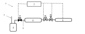
図1~4は、様々なパルシング法を組み込むシステム構成1を例示する。いくつかの実施形態では、システム構成1は、キャリアガスライン2と、キャリアガスライン2の下流にあり、キャリアガスライン2と流体連通している反応物質供給源3と、供給源3の下流の中間チャンバー4と、中間チャンバー4の下流の反応器5と、複数のバルブ、V1、V2、およびV3と、を備える。反応物質供給ライン6は供給源3を中間チャンバー4に連結し、バルブV1は供給源3と中間チャンバー4との間の反応物質供給ライン6に取り付けられる。反応物質供給ライン6は中間チャンバー4を反応器5に連結し、複数のバルブV2およびV3は中間チャンバー4と反応器5との間のライン6に取り付けられる。バルブV1、V2、およびV3は、任意の好適なタイプのバルブを備えることができる。例えば、様々な実施形態では、バルブV1およびV2は、複数の流動コンダクタンスを有する調整可能なバルブを備えることができる。いくつかの実施形態では、バルブV1およびV2は、バイナリオン/オフバルブを備えることができる。いくつかの実施形態では、バルブV3は、所望の流動コンダクタンスに調節できるニードルバルブを備えることができる。図1~4に示すように、制御システム7は、バルブV1、V2、V3の動作(例えば、開閉)、および/またはシステムの他の構成要素例えば反応器の構成要素の動作を制御するように構成される処理回路を備えることができる。例示されていないが、制御システム7はまた、様々なタイプのセンサ、例えば、中間チャンバー4、供給源3、反応器5、またはシステムの任意の他の好適な構成要素もしくはガスラインの圧力を監視するように構成される圧力センサと電気的に通信することができる。制御システム7は、他の構成要素、例えばヒーターと電気的に通信することができる。さらに、図示しないが、システム1において、例えば、中間チャンバー4の上流および/またはバルブV1、V2、V3のいずれかの上流にフィルターを設けることができる。
1-4
いくつかの実施形態では、供給源3は、液体または固体材料を蒸気に変換するように構成される気化器を備える。例えば、供給源3は、バブラー、蒸発器、液体インジェクター、固体供給源昇華器などを備えることができる。供給源3は、気化した反応物質を反応物質供給ライン6に供給することができる。様々な実施形態では、供給源3は、エッチングプロセスの反応物質(例えば、エッチャント)を含むことができる。キャリアガスは、示すように気化器と共に使用されることができ、天然ガス反応物質を運ぶ/希釈するためにも使用されることもできる。その他の実施形態では、キャリアガスは使用されない。
In some embodiments,
いくつかの実施形態では、システム構成1は、プラズマ、ラジカルおよび励起種の供給源を備えない。いくつかの実施形態では、システム構成1は、プラズマ、ラジカルまたは励起種の形成のためのRFも、マイクロ波も、ICP源も含まない。いくつかの実施形態では、システム構成1は互換性がなく、プラズマベースのプロセスに使用されることができない。
In some embodiments,
図1は、気化した反応物質が中間チャンバー4に供給され、その中に保持される、充填段階にあるシステム1を例示する。例えば、図1では、バルブV1が開き、中間チャンバー4をキャリアガスと気化した反応物質の混合物で所望の圧力まで充填することができる。いくつかの実施形態では、バルブV1は、気化した反応物質の流動コンダクタンスを制御できる調整可能なバルブとすることができる。中間チャンバー4は、反応物質が反応器5への送達のために蒸気形態のままであることを確実にすることができるチャンバーを備えることができる。いくつかの実施形態では、制御システム7はまた、例えば、バルブV1、V2のうちの一つまたは複数を開閉することによって、反応器5に供給される反応物質蒸気の量を測定または制御することができる。したがって、制御システム7は、反応器5へのパルス送達のパルス幅およびタイミングを制御するように構成されることができる。いくつかの実施形態では、反応器5へのパルスは、約0.001秒~60秒の範囲のパルス幅を有することができる。例えば、パルス幅は、約0.01秒~10秒の範囲、約0.05秒~10秒の範囲、または約0.1秒~5秒の範囲とすることができる。いくつかの実施形態では、パルスのパルス高さに関連する分圧は、約0.001mbar~100mbarの範囲とすることができる。例えば、パルスのパルス高さに関連する分圧は、約0.05mbar~50mbarの範囲、または約0.1mbar~20mbarの範囲とすることができる。バルブV2を開けて、反応器5にキャリアガスと気化した反応物質との混合物を供給することができる。いくつかの実施形態では、バルブV2は、気化した反応物質の流動コンダクタンスを制御できる調整可能なバルブとすることができる。いくつかの実施形態では、バルブV3は、気化した反応物質の流動コンダクタンスを制御するニードルバルブとすることができる。
FIG. 1 illustrates
いくつかの実施形態では、システム構成1は、ヒーターまたは他の加熱装置によって様々な温度に維持される一つまたは複数の熱ゾーンを備えることができる。いくつかの実施形態では、気化器、中間チャンバー4、および反応チャンバーに対して別個の熱ゾーンがあり、各熱ゾーンは第一、第二、および第三の温度をそれぞれ有する。いくつかの実施形態では、第一、第二および第三の温度はほぼ等しい。いくつかの実施形態では、第二の熱ゾーンの第二の温度は、第一の熱ゾーンの第一の温度よりも高くすることができる。様々な実施形態では、例えば、第二の温度は、5℃~50℃の範囲、5℃~35℃の範囲、または10℃~25℃の範囲の温度差で、第一の温度よりも高くてもよい。いくつかの実施形態では、第一の熱ゾーンの第一の温度は、第二の熱ゾーンの第二の温度よりも高くすることができる。いくつかの実施形態では、キャリアガスライン2の部分にヒータージャケット設けて、ライン2をそのそれぞれの熱ゾーンの温度以上で、反応物質の凝縮温度を超えて維持することができる。
In some embodiments, the
システム1は、様々なエッチングモードで動作することができる。図1において、中間チャンバー4は、気化した反応物質およびキャリアガスで、所望のまたは設定点圧力まで充填されることができ、これは、所望の反応物質の分圧と相関することができる。反応物質蒸気を供給源3で気化させることができる。バルブV1を開ける場合、気化した反応物質とキャリアガスとの混合物を運ぶことができ、反応物質供給ライン6に沿って中間チャンバー4に送達することができる。図2~3に示すように、中間チャンバー4はP1の圧力に充填されることができ、そしてバルブV1を閉じることができる。中間チャンバー4内の気化した反応物質のドーズ量は、式nR=P1V/Tによって決定されることができる。
図2は、第一のタイプまたは形状のパルスが反応器5に送達される第一のエッチングモードを例示する。上記で説明したように、バルブV1を閉じることができ、バルブV2を少なくとも部分的に開けることができる。中間チャンバー4に含まれる反応物質蒸気のドーズ量の一部は、反応器5に搬送されることができる。パルス期間中の反応物質の分圧は、少なくとも部分的にニードルバルブV3のコンダクタンス、および中間チャンバー4内の圧力、P1と、反応器5内の圧力、P2との間の圧力差によって決定されることができる。いくつかの実施形態では、圧力P1は、約0.001mbar~100mbarの範囲とすることができる。例えば、圧力P1は、約0.05mbar~50mbarの範囲、または約0.1mbar~20mbarの範囲とすることができる。いくつかの実施形態では、圧力P2は、約0.001mbar~100mbarの範囲とすることができる。例えば、圧力P2は、約0.05mbar~50mbarの範囲、または約0.1mbar~20mbarの範囲とすることができる。様々な実施形態では、P1のP2に対する比は、約100:1、50:1、10:1、5:1、3:1、2:1、1.5:1、1.25:1、または1.1:1未満とすることができる。圧力差は、式ΔP=P1-P2によって決定される。動作中、圧力差ΔPはバルブV2を開けた後に圧力P1が減少するにつれて一定に変化する。したがって、反応チャンバー5内の反応物質の分圧はまた、時間の関数を変化させることができ、コンダクタンスがパルス中に一定に保たれる場合、線形であることもできる。図2に示すように、パルスの終わりの前駆体テールは、V2を遮断した後、V2とV3との間の容積から前駆体ガスが流出することによって引き起こされる可能性がある。いくつかの実施形態では、パルスの前半の最大分圧と比較すると、パルスの後半の分圧は約75%未満である。別の実施形態では、パルスの前半の最大分圧と比較すると、パルスの後半の分圧は約50%未満である。別の実施形態では、パルスの前半の最大分圧と比較すると、パルスの後半の分圧は約25%未満である。例示のパルスは、パルスまたは周期的化学気相エッチングプロセスで周期的に繰り返されることができる。
2 illustrates a first etching mode in which a pulse of a first type or shape is delivered to the
図3は、第二のタイプまたは形状のパルスが反応器5に送達される第二のエッチングモードを例示する。中間チャンバー4の充填容積の一部のみが使用される図2の第一のモードとは異なり、図3の第二のモードでは、中間チャンバー4を充填する全てのまたは実質的に全ての反応物質蒸気が使用されてもよい、例えば、反応チャンバー5に送達されてもよい。図3に示すように、バルブV1は閉じられてもよい。バルブV2を開けることができ、また中間チャンバー4内に含まれる反応物質の蒸気のドーズ量の少なくとも一部を、充填容量(例えば、中間チャンバー4)と反応器5との間の圧力が同じ(ΔP=0)になるまで反応器5に搬送されることができる。このパルス期間中の気化した反応物質の分圧は、ニードルバルブV3のコンダクタンス、および中間チャンバー4の圧力P1と反応器5の圧力P2との間の圧力の差によって決定されることができる。圧力の差は、式ΔP=P1-P2によって決定される。動作中、バルブV2を開けた後に圧力P1が減少するにつれて、圧力差ΔPは常に変化する可能性がある。したがって、反応チャンバー5に送達される反応物質の分圧はまた、コンダクタンスが一定に保持される場合、時間と共に、また直線的に変化することができる。図3に示すように、気化した反応物質の分圧は、バルブV2を開けた後に直線的に減少することができる。いくつかの実施形態では、分圧は毎秒10%を超える速度で減少する可能性がある。例えば、分圧は、毎秒約25%を超える速度で、毎秒約50%を超える速度で、または毎秒約75%を超える速度で減少する可能性がある。様々な実施形態では、気化した反応物質の分圧は、バルブV2を開けた後にほぼ直線的に減少することができる。図2に示す第一のモードとは異なり、図3の第二のモードでは、このパルスモードには分圧テールがない場合がある。気化した反応物質のドーズ量は、式[P1(0)-P2]V/Tによって決定されることができ、ここでP1(0)はV2を開ける前の中間チャンバー4の圧力であり、P2は反応器の圧力である。例示のパルスは、パルスまたは周期的化学気相エッチングプロセスで周期的に繰り返されることができる。
3 illustrates a second etching mode in which a pulse of a second type or shape is delivered to the
図4は、第三のタイプまたは形状のパルスが反応器5に送達される第三のエッチングモードを例示する。図4に示す第三のモードでは、V1およびV2の両方をパルス中に開け、これにより気化した反応物質を供給源3から中間チャンバー4を通して反応器5に搬送する。パルス時間の間の反応物質の分圧は、供給源容器3の圧力およびニードルバルブV3のコンダクタンスによって、少なくとも部分的に決定されることができる。供給源容器3内の前駆体の気化速度およびコンダクタンスがパルス中に一定である場合、分圧もパルス中に一定のままであることができる。図2の前駆体テールに関連して上で説明したのと概ね同様の理由で、図4に示すように、パルスの終端部で前駆体テールが存在する場合もある。例示のパルスは、パルスまたは周期的化学気相エッチングプロセスで周期的に繰り返されることができる。この第三のエッチングモードの動作は、このようなチャンバーのない装置と比較して、中間チャンバーの存在による影響を受けない可能性があるが、これらおよび他の所望のモードを達成し、かつ反応チャンバー内の基材全体で所望のエッチング分布と効果を達成するように調整する別の変数を提供するための装置の動作の適応性を示す。別の実施形態では、この第三のエッチングモードの動作は、このようなチャンバーのない装置と比較して、中間チャンバーの存在による影響を受ける可能性があるが、これらおよび他の所望のモードを達成し、かつ反応チャンバー内の基材全体で所望のエッチング分布と効果を達成するように調整する別の変数を提供するための装置の動作の適応性を示す。
4 illustrates a third etch mode in which a third type or shape of pulse is delivered to the
有益なことに、本明細書に開示されるシステムおよび方法は、様々なタイプのエッチング、例えばALEの手順における改善された空間的均一性および共形性を提供することができる。供給源3と反応器5との間にバルブV1、V2、およびV3を備える中間チャンバー4を使用することにより、パルス中の全体的なドーズ量および分圧の制御を提供することができる。異なるパルスモードを選択して、所望のパルス形状を反応器5に提供することもできる。
Advantageously, the systems and methods disclosed herein can provide improved spatial uniformity and conformality in various types of etching, e.g., ALE procedures. The use of an
本発明の特定の実施形態を記載したが、これらの実施形態は例として提示したにすぎず、本開示の範囲を限定することを意図していない。実際、本明細書に記載されている新規の方法およびシステムは、様々な他の形態で具体化されることができる。さらに、本明細書に記載のシステムおよび方法における様々な省略、置換、および変更は、本開示の趣旨から逸脱することなく行われることができる。添付の特許請求の範囲およびそれらの均等物は、本開示の範囲および趣旨に含まれるような形態または修正を網羅することを意図する。したがって、本発明の範囲は、添付の特許請求の範囲を参照することによってのみ定義される。 Although specific embodiments of the present invention have been described, these embodiments are presented by way of example only and are not intended to limit the scope of the disclosure. Indeed, the novel methods and systems described herein may be embodied in a variety of other forms. Furthermore, various omissions, substitutions, and modifications in the systems and methods described herein may be made without departing from the spirit of the disclosure. The appended claims and their equivalents are intended to cover such forms or modifications as are within the scope and spirit of the disclosure. Accordingly, the scope of the present invention is defined solely by reference to the appended claims.
特定の態様、実施形態、または実施例に関連して記載の特徴、材料、特性、またはグループは、それと矛盾しなければ、この節または本明細書の他の場所に記載の他の任意の態様、実施形態、または実施例に適用可能であると理解されるべきである。(添付の特許請求の範囲、要約、および図面を含む)本明細書に開示されている全ての特徴、および/またはそのように開示されている任意の方法またはプロセスの全ての工程は、このような特徴および/または工程のうちの少なくともいくつかが相互に排他的である組み合わせを除いて、任意の組み合わせで組み合わせることができる。保護は、全ての前述の実施形態の詳細に限定されることはない。保護は、本明細書に開示される特徴(添付の特許請求の範囲、要約、および図面を含む)の新規のもの、もしくは新規の組み合わせ、またはそのように開示される任意の方法もしくはプロセスの工程の、任意の新規のものもしくは任意の新規の組み合わせにまで及ぶ。 It should be understood that features, materials, properties, or groups described in connection with a particular aspect, embodiment, or example are applicable to any other aspect, embodiment, or example described in this section or elsewhere in this specification, unless inconsistent therewith. All features disclosed herein (including the accompanying claims, abstract, and drawings), and/or all steps of any method or process so disclosed, may be combined in any combination, except combinations in which at least some of such features and/or steps are mutually exclusive. Protection is not limited to the details of all the foregoing embodiments. Protection extends to any novel or novel combination of features disclosed herein (including the accompanying claims, abstract, and drawings), or any novel or novel combination of steps of any method or process so disclosed.
さらに、別個の実施形態に関連して本開示に記載されている特定の特徴はまた、単一の実施形態において組み合わせて実施されることができる。逆に、単一の実施形態に関連して記載の様々な特徴も、複数の実施形態で別々に、または任意の好適な部分的組み合わせで実施されることができる。さらに、特徴は特定の組み合わせで機能するものとして上に記載されるが、特許請求される組み合わせからの一つまたは複数の特徴は、場合により組み合わせから削除されることができ、組み合わせは、部分的組み合わせまたは部分的組み合わせの変形として特許請求されてもよい。 Furthermore, certain features that are described in the present disclosure in the context of separate embodiments can also be implemented in combination in a single embodiment. Conversely, various features that are described in the context of a single embodiment can also be implemented in multiple embodiments separately or in any suitable subcombination. Furthermore, although features are described above as functioning in a particular combination, one or more features from a claimed combination can, in some cases, be deleted from the combination, and the combination may be claimed as a subcombination or a variation of the subcombination.
さらに、操作は特定の順序で図面に描かれてもよい、または特定の順序で本明細書に記載されることができるが、このような操作は、望ましい結果を達成するために、示される特定の順序もしくは順次に実行される必要もなく、全ての操作が実行される必要もない。図示または記載されていない他の操作は、例示的な方法およびプロセスに組み込まれることができる。例えば、一つまたは複数の追加の操作は、記載される操作のいずれかの前、後、同時、または間に実行されることができる。さらに、他の実施形態では、操作を組み替えるまたは並べ替えることができる。当業者は、いくつかの実施形態では、図示および/または開示されたプロセスで行われる実際の工程は、図に示される工程と異なる場合があることを理解するであろう。実施形態に応じて、上記の工程のうちのいくつかは削除されてもよく、他の工程が追加されてもよい。さらに、上に開示された特定の実施形態の特徴および属性は、追加の実施形態を形成するために異なる方法で組み合わされてもよく、それらの全ては本開示の範囲内に含まれる。また、上記の実施形態における様々なシステム構成要素の分離は、全ての実施形態においてこのような分離を必要としていると理解されるべきではない。そして、記載の構成要素およびシステムは、一般的に、単一の製品に一緒に統合されるか、または複数の製品にパッケージされることができることを理解されたい。 Furthermore, although operations may be depicted in the figures or described herein in a particular order, such operations need not be performed in the particular order or sequence shown, nor need all operations be performed, to achieve desirable results. Other operations not shown or described can be incorporated into the exemplary methods and processes. For example, one or more additional operations can be performed before, after, simultaneously, or between any of the described operations. Furthermore, in other embodiments, operations can be rearranged or reordered. Those skilled in the art will appreciate that in some embodiments, the actual steps performed in the illustrated and/or disclosed processes may differ from those shown in the figures. Depending on the embodiment, some of the above steps may be omitted and other steps may be added. Furthermore, the features and attributes of certain embodiments disclosed above may be combined in different ways to form additional embodiments, all of which are within the scope of the present disclosure. Also, the separation of various system components in the above embodiments should not be understood as requiring such separation in all embodiments. And, it should be understood that the components and systems described can generally be integrated together in a single product or packaged in multiple products.
この開示の目的のために、いくつかの態様、利点、および新規の特徴が本明細書に記載されている。必ずしも全てのこのような利点が任意の特定の実施形態に従って達成されるとは限らない。したがって、例えば、当業者は、本開示が、本明細書で教示または示唆されることができる他の利点を必ずしも達成することなく、本明細書で教示される一つの利点または一群の利点を達成する方法で具体化または実行されることができることを認識するであろう。 For purposes of this disclosure, certain aspects, advantages, and novel features have been described herein. Not necessarily all such advantages are achieved in accordance with any particular embodiment. Thus, for example, one skilled in the art will recognize that the present disclosure can be embodied or carried out in a manner that achieves one advantage or group of advantages taught herein without necessarily achieving other advantages that may be taught or suggested herein.
条件付き用語、例えば「できる(can)」、「できるであろう(could)」、「してもよい(might)」、「できる(may)」は、特に記載のない限り、または使用されている文脈内で理解されていない限り、特定の実施形態は特定の特徴、要素および/または工程を含むが、他の実施形態は含まないことを伝えることを一般的に意図していることが理解されよう。したがって、このような条件付き言語は、特徴、要素、および/もしくは工程が一つもしくは複数の実施形態になんらかの形で必要とされること、または一つもしくは複数の実施形態は、ユーザーの入力もしくは指示の有無にかかわらず、これらの特徴、要素および/もしくは工程が任意の特定の実施形態に含まれるか実行されるかを決定するためのロジックを必ず含むことを示唆することを一般的に意図していない。 It will be understood that conditional language, e.g., "can," "could," "might," and "may," are generally intended to convey that certain embodiments include certain features, elements, and/or steps, but other embodiments do not, unless otherwise indicated or understood within the context in which they are used. Thus, such conditional language is not generally intended to suggest that the features, elements, and/or steps are somehow required in one or more embodiments, or that one or more embodiments necessarily include logic for determining whether those features, elements, and/or steps are included or performed in any particular embodiment, with or without user input or direction.
接続語、例えば語句「X、Y、およびZのうちの少なくとも一つ」は、特に記載のない限り、そうでなければアイテム、用語などがX、Y、またはZのいずれかであることを伝えるために一般的に使用される文脈で理解される。したがって、このような接続語は、特定の実施形態がXのうちの少なくとも一つ、Yのうちの少なくとも一つ、およびZのうちの少なくとも一つの存在を必要とすることを示唆することを一般に意図するものではない。 Conjunctions, such as the phrase "at least one of X, Y, and Z," are understood in the context in which they are otherwise commonly used to convey that an item, term, etc. is either X, Y, or Z, unless otherwise noted. Thus, such conjunctions are not generally intended to suggest that a particular embodiment requires the presence of at least one of X, at least one of Y, and at least one of Z.
本明細書で使用される度合いの用語、例えば本明細書で使用する用語「およそ」、「約」、「一般的に」および「実質的に」は、依然として所望の機能を実施する、または所望の結果を達成する、記載された値、量、もしくは特性に近い値、量、もしくは特性を表す。例えば、用語「およそ」、「約」、「一般的に」、および「実質的に」は、記載の量の10%未満以内、5%未満以内、1%未満以内、0.1%未満以内、および0.01%未満以内の量を指す場合がある。別の例として、特定の実施形態では、用語「概ね平行」および「実質的に平行」は、正確な平行から15度、10度、5度、3度、1度、または0.1度以下離れている値、量、または特性を意味する。 Degree terms used herein, such as the terms "approximately," "about," "generally," and "substantially" as used herein, refer to a value, amount, or characteristic that is close to the stated value, amount, or characteristic that still performs a desired function or achieves a desired result. For example, the terms "approximately," "about," "generally," and "substantially" may refer to an amount that is within 10%, 5%, 1%, 0.1%, and 0.01% of the stated amount. As another example, in certain embodiments, the terms "generally parallel" and "substantially parallel" refer to a value, amount, or characteristic that is 15 degrees, 10 degrees, 5 degrees, 3 degrees, 1 degree, or 0.1 degrees or less away from exact parallelism.
本開示の範囲は、この節または本明細書の他の場所において好ましい実施形態の特定の開示によって限定されることを意図していない、およびこの節もしくは本明細書の他の場所で提示される、または将来提示される特許請求の範囲によって定義されることができる。特許請求の範囲の用語は、特許請求の範囲で使用される用語に基づいて広く解釈されるべきであり、本明細書にまたは出願手続き中に記載された実施例に限定されず、その実施例は非限定的であると解釈されるべきである。
The scope of the present disclosure is not intended to be limited by the specific disclosure of preferred embodiments in this section or elsewhere herein, and may be defined by the claims presented in this section or elsewhere herein, or presented in the future. The claim terms are to be interpreted broadly based on the terms used in the claims, and are not limited to the examples described herein or during the prosecution, which examples are to be construed as non-limiting.
Claims (24)
反応チャンバーと、
前記反応チャンバーの上流にあり前記反応チャンバーと流体連通している中間チャンバーであって、エッチング反応物質蒸気を前記反応チャンバーに送達するように構成される、中間チャンバーと、
前記中間チャンバーの上流にあり前記中間チャンバーと流体連通しているエッチング反応物質蒸気の供給源であって、前記エッチング反応物質蒸気を前記中間チャンバーに送達するように構成される、供給源と、
前記供給源と前記中間チャンバーとの間の反応物質供給ラインに沿って配置される第一のバルブであって、前記中間チャンバーへの前記エッチング反応物質蒸気の流量を調整するように構成される、第一のバルブと、
前記中間チャンバーと前記反応チャンバーとの間の前記反応物質供給ラインに沿って配置される第二のバルブであって、前記反応チャンバーへの前記エッチング反応物質蒸気の流量を調整するように構成される、第二のバルブと、を備える、半導体エッチング装置。 A semiconductor etching apparatus comprising:
A reaction chamber;
an intermediate chamber upstream of and in fluid communication with the reaction chamber, the intermediate chamber configured to deliver an etching reactant vapor to the reaction chamber;
a source of etching reactant vapor upstream of the intermediate chamber and in fluid communication with the intermediate chamber, the source configured to deliver the etching reactant vapor to the intermediate chamber;
a first valve disposed along a reactant supply line between the source and the intermediate chamber, the first valve configured to regulate a flow rate of the etching reactant vapor to the intermediate chamber;
a second valve disposed along the reactant supply line between the intermediate chamber and the reaction chamber, the second valve configured to adjust a flow rate of the etch reactant vapor to the reaction chamber.
反応チャンバーと、
前記反応チャンバーの上流にあり前記反応チャンバーと流体連通している中間チャンバーであって、エッチング反応物質蒸気を前記反応チャンバーに送達するように構成される、中間チャンバーと、
前記エッチング反応物質蒸気を前記中間チャンバーから前記反応チャンバー内にパルスするように構成される制御システムと、を備える、装置。 A semiconductor etching apparatus comprising:
A reaction chamber;
an intermediate chamber upstream of and in fluid communication with the reaction chamber, the intermediate chamber configured to deliver an etching reactant vapor to the reaction chamber;
and a control system configured to pulse the etch reactant vapor from the intermediate chamber into the reaction chamber.
エッチング反応物質蒸気を中間チャンバーに供給することと、
前記エッチング反応物質蒸気の少なくとも一部を前記中間チャンバーから前記中間チャンバーの下流にある反応チャンバーへパルスすることと、を含む方法。 1. A method of etching a substrate, the method comprising:
providing an etching reactant vapor to the intermediate chamber;
and pulsing at least a portion of the etching reactant vapor from the intermediate chamber to a reaction chamber downstream of the intermediate chamber.
22. The method of claim 21 , wherein pulsing at least a portion of the etch reactant vapor comprises opening the first valve and opening a second valve downstream of the first valve to deliver at least a portion of the etch reactant vapor to the reaction chamber.
Applications Claiming Priority (3)
| Application Number | Priority Date | Filing Date | Title |
|---|---|---|---|
| US201962875910P | 2019-07-18 | 2019-07-18 | |
| US62/875,910 | 2019-07-18 | ||
| JP2020121150A JP7548740B2 (en) | 2019-07-18 | 2020-07-15 | Semiconductor vapor phase etching apparatus with intermediate chamber |
Related Parent Applications (1)
| Application Number | Title | Priority Date | Filing Date |
|---|---|---|---|
| JP2020121150A Division JP7548740B2 (en) | 2019-07-18 | 2020-07-15 | Semiconductor vapor phase etching apparatus with intermediate chamber |
Publications (2)
| Publication Number | Publication Date |
|---|---|
| JP2024164243A true JP2024164243A (en) | 2024-11-26 |
| JP7738140B2 JP7738140B2 (en) | 2025-09-11 |
Family
ID=74171392
Family Applications (2)
| Application Number | Title | Priority Date | Filing Date |
|---|---|---|---|
| JP2020121150A Active JP7548740B2 (en) | 2019-07-18 | 2020-07-15 | Semiconductor vapor phase etching apparatus with intermediate chamber |
| JP2024147651A Active JP7738140B2 (en) | 2019-07-18 | 2024-08-29 | Semiconductor vapor phase etching apparatus with intermediate chamber |
Family Applications Before (1)
| Application Number | Title | Priority Date | Filing Date |
|---|---|---|---|
| JP2020121150A Active JP7548740B2 (en) | 2019-07-18 | 2020-07-15 | Semiconductor vapor phase etching apparatus with intermediate chamber |
Country Status (5)
| Country | Link |
|---|---|
| US (2) | US20210020469A1 (en) |
| JP (2) | JP7548740B2 (en) |
| KR (1) | KR102746606B1 (en) |
| CN (1) | CN112242322B (en) |
| TW (1) | TWI851769B (en) |
Families Citing this family (4)
| Publication number | Priority date | Publication date | Assignee | Title |
|---|---|---|---|---|
| CN110050331B (en) | 2016-12-09 | 2023-07-25 | Asm Ip 控股有限公司 | Thermal Atomic Layer Etching Process |
| US10283319B2 (en) | 2016-12-22 | 2019-05-07 | Asm Ip Holding B.V. | Atomic layer etching processes |
| JP7737789B2 (en) | 2019-07-18 | 2025-09-11 | エーエスエム・アイピー・ホールディング・ベー・フェー | Showerhead device for semiconductor processing system |
| US11574813B2 (en) | 2019-12-10 | 2023-02-07 | Asm Ip Holding B.V. | Atomic layer etching |
Citations (10)
| Publication number | Priority date | Publication date | Assignee | Title |
|---|---|---|---|---|
| JPS57104664A (en) * | 1980-12-03 | 1982-06-29 | Fujitsu Ltd | Gasification method for liquid source |
| JPS6378533A (en) * | 1986-09-20 | 1988-04-08 | Fujitsu Ltd | Etching device |
| JPH11102891A (en) * | 1997-09-29 | 1999-04-13 | Dainippon Screen Mfg Co Ltd | Substrate processing equipment |
| WO2007114156A1 (en) * | 2006-03-30 | 2007-10-11 | Mitsui Engineering & Shipbuilding Co., Ltd. | Atomic layer growing apparatus |
| JP2010147388A (en) * | 2008-12-22 | 2010-07-01 | Tokyo Electron Ltd | Method and apparatus for supplying mixed gas |
| US20100267242A1 (en) * | 2009-04-20 | 2010-10-21 | Xactix, Inc. | Selective Etching Of Semiconductor Substrate(s) That Preserves Underlying Dielectric Layers |
| JP2015192150A (en) * | 2014-03-27 | 2015-11-02 | ラム リサーチ コーポレーションLam Research Corporation | Method of etching non-volatile metal materials |
| US20160293398A1 (en) * | 2015-04-03 | 2016-10-06 | Lam Research Corporation | Deposition of conformal films by atomic layer deposition and atomic layer etch |
| US20180174826A1 (en) * | 2016-12-15 | 2018-06-21 | Asm Ip Holding B.V. | Sequential infiltration synthesis apparatus |
| JP2019083265A (en) * | 2017-10-31 | 2019-05-30 | 株式会社日立ハイテクノロジーズ | Apparatus for manufacturing semiconductor and method of manufacturing semiconductor device |
Family Cites Families (16)
| Publication number | Priority date | Publication date | Assignee | Title |
|---|---|---|---|---|
| US3184978A (en) * | 1963-04-17 | 1965-05-25 | Ford Motor Co | Fluid pressure governor mechanism |
| JPS58161775A (en) * | 1982-03-19 | 1983-09-26 | Anelva Corp | Discharging device |
| JP3830670B2 (en) * | 1998-09-03 | 2006-10-04 | 三菱電機株式会社 | Semiconductor manufacturing equipment |
| JP2002353205A (en) * | 2000-08-28 | 2002-12-06 | Mitsubishi Electric Corp | Semiconductor device manufacturing method, wafer processing apparatus used therefor, and semiconductor device |
| CN100454200C (en) * | 2003-06-09 | 2009-01-21 | 喜开理株式会社 | Relative pressure control system and relative flow control system |
| US20060207503A1 (en) * | 2005-03-18 | 2006-09-21 | Paul Meneghini | Vaporizer and method of vaporizing a liquid for thin film delivery |
| JP4595702B2 (en) * | 2004-07-15 | 2010-12-08 | 東京エレクトロン株式会社 | Film forming method, film forming apparatus, and storage medium |
| JP2010087169A (en) * | 2008-09-30 | 2010-04-15 | Tokyo Electron Ltd | Carburetor and film-forming system using the same |
| US8724974B2 (en) * | 2011-09-30 | 2014-05-13 | Fujikin Incorporated | Vaporizer |
| US20130312663A1 (en) * | 2012-05-22 | 2013-11-28 | Applied Microstructures, Inc. | Vapor Delivery Apparatus |
| US9447497B2 (en) * | 2013-03-13 | 2016-09-20 | Applied Materials, Inc. | Processing chamber gas delivery system with hot-swappable ampoule |
| US9263350B2 (en) * | 2014-06-03 | 2016-02-16 | Lam Research Corporation | Multi-station plasma reactor with RF balancing |
| US9576811B2 (en) * | 2015-01-12 | 2017-02-21 | Lam Research Corporation | Integrating atomic scale processes: ALD (atomic layer deposition) and ALE (atomic layer etch) |
| US9904299B2 (en) * | 2015-04-08 | 2018-02-27 | Tokyo Electron Limited | Gas supply control method |
| US10079150B2 (en) * | 2015-07-23 | 2018-09-18 | Spts Technologies Limited | Method and apparatus for dry gas phase chemically etching a structure |
| CN110050331B (en) * | 2016-12-09 | 2023-07-25 | Asm Ip 控股有限公司 | Thermal Atomic Layer Etching Process |
-
2020
- 2020-07-15 JP JP2020121150A patent/JP7548740B2/en active Active
- 2020-07-16 US US16/930,867 patent/US20210020469A1/en not_active Abandoned
- 2020-07-16 TW TW109124031A patent/TWI851769B/en active
- 2020-07-16 CN CN202010684945.5A patent/CN112242322B/en active Active
- 2020-07-16 KR KR1020200088297A patent/KR102746606B1/en active Active
-
2024
- 2024-08-29 JP JP2024147651A patent/JP7738140B2/en active Active
-
2025
- 2025-09-18 US US19/332,551 patent/US20260018432A1/en active Pending
Patent Citations (10)
| Publication number | Priority date | Publication date | Assignee | Title |
|---|---|---|---|---|
| JPS57104664A (en) * | 1980-12-03 | 1982-06-29 | Fujitsu Ltd | Gasification method for liquid source |
| JPS6378533A (en) * | 1986-09-20 | 1988-04-08 | Fujitsu Ltd | Etching device |
| JPH11102891A (en) * | 1997-09-29 | 1999-04-13 | Dainippon Screen Mfg Co Ltd | Substrate processing equipment |
| WO2007114156A1 (en) * | 2006-03-30 | 2007-10-11 | Mitsui Engineering & Shipbuilding Co., Ltd. | Atomic layer growing apparatus |
| JP2010147388A (en) * | 2008-12-22 | 2010-07-01 | Tokyo Electron Ltd | Method and apparatus for supplying mixed gas |
| US20100267242A1 (en) * | 2009-04-20 | 2010-10-21 | Xactix, Inc. | Selective Etching Of Semiconductor Substrate(s) That Preserves Underlying Dielectric Layers |
| JP2015192150A (en) * | 2014-03-27 | 2015-11-02 | ラム リサーチ コーポレーションLam Research Corporation | Method of etching non-volatile metal materials |
| US20160293398A1 (en) * | 2015-04-03 | 2016-10-06 | Lam Research Corporation | Deposition of conformal films by atomic layer deposition and atomic layer etch |
| US20180174826A1 (en) * | 2016-12-15 | 2018-06-21 | Asm Ip Holding B.V. | Sequential infiltration synthesis apparatus |
| JP2019083265A (en) * | 2017-10-31 | 2019-05-30 | 株式会社日立ハイテクノロジーズ | Apparatus for manufacturing semiconductor and method of manufacturing semiconductor device |
Also Published As
| Publication number | Publication date |
|---|---|
| JP2021019202A (en) | 2021-02-15 |
| JP7548740B2 (en) | 2024-09-10 |
| KR102746606B1 (en) | 2024-12-24 |
| CN112242322B (en) | 2025-08-26 |
| KR20210010831A (en) | 2021-01-28 |
| JP7738140B2 (en) | 2025-09-11 |
| TW202109682A (en) | 2021-03-01 |
| US20210020469A1 (en) | 2021-01-21 |
| TWI851769B (en) | 2024-08-11 |
| US20260018432A1 (en) | 2026-01-15 |
| CN112242322A (en) | 2021-01-19 |
Similar Documents
| Publication | Publication Date | Title |
|---|---|---|
| JP7738140B2 (en) | Semiconductor vapor phase etching apparatus with intermediate chamber | |
| JP7760009B2 (en) | Variable cycle and time RF activation method for film thickness matching in a multi-station deposition system | |
| KR20220119586A (en) | Systems and methods for vapor delivery | |
| KR100979575B1 (en) | Atomic layer deposition apparatus and manufacturing method thereof | |
| US6905737B2 (en) | Method of delivering activated species for rapid cyclical deposition | |
| TWI793197B (en) | Devices and methods for atomic layer deposition | |
| US20090035946A1 (en) | In situ deposition of different metal-containing films using cyclopentadienyl metal precursors | |
| US9605346B2 (en) | Systems and methods for pressure-based liquid flow control | |
| JP7625540B2 (en) | Independently adjustable channel conductance in multi-station semiconductor processing - Patents.com | |
| KR20130129863A (en) | Systems and methods for modulating step coverage during conformal film deposition | |
| KR20210005523A (en) | Liquid vaporizer | |
| US20260009127A1 (en) | Semiconductor processing device | |
| CN113718231A (en) | System and method for direct liquid injection of vanadium precursors | |
| JP2023098683A (en) | Gas supply unit and substrate processing apparatus including gas supply unit |
Legal Events
| Date | Code | Title | Description |
|---|---|---|---|
| A521 | Request for written amendment filed |
Free format text: JAPANESE INTERMEDIATE CODE: A523 Effective date: 20240926 |
|
| A621 | Written request for application examination |
Free format text: JAPANESE INTERMEDIATE CODE: A621 Effective date: 20240926 |
|
| TRDD | Decision of grant or rejection written | ||
| A01 | Written decision to grant a patent or to grant a registration (utility model) |
Free format text: JAPANESE INTERMEDIATE CODE: A01 Effective date: 20250805 |
|
| A61 | First payment of annual fees (during grant procedure) |
Free format text: JAPANESE INTERMEDIATE CODE: A61 Effective date: 20250901 |
|
| R150 | Certificate of patent or registration of utility model |
Ref document number: 7738140 Country of ref document: JP Free format text: JAPANESE INTERMEDIATE CODE: R150 |