JP2024134721A - Spectroscopic and profilometric instruments - Google Patents
Spectroscopic and profilometric instruments Download PDFInfo
- Publication number
- JP2024134721A JP2024134721A JP2023045064A JP2023045064A JP2024134721A JP 2024134721 A JP2024134721 A JP 2024134721A JP 2023045064 A JP2023045064 A JP 2023045064A JP 2023045064 A JP2023045064 A JP 2023045064A JP 2024134721 A JP2024134721 A JP 2024134721A
- Authority
- JP
- Japan
- Prior art keywords
- light
- signal
- light source
- emitted
- analytical
- Prior art date
- Legal status (The legal status is an assumption and is not a legal conclusion. Google has not performed a legal analysis and makes no representation as to the accuracy of the status listed.)
- Pending
Links
Images


Classifications
-
- G—PHYSICS
- G01—MEASURING; TESTING
- G01J—MEASUREMENT OF INTENSITY, VELOCITY, SPECTRAL CONTENT, POLARISATION, PHASE OR PULSE CHARACTERISTICS OF INFRARED, VISIBLE OR ULTRAVIOLET LIGHT; COLORIMETRY; RADIATION PYROMETRY
- G01J3/00—Spectrometry; Spectrophotometry; Monochromators; Measuring colours
- G01J3/28—Investigating the spectrum
- G01J3/45—Interferometric spectrometry
- G01J3/453—Interferometric spectrometry by correlation of the amplitudes
- G01J3/4535—Devices with moving mirror
-
- G—PHYSICS
- G01—MEASURING; TESTING
- G01B—MEASURING LENGTH, THICKNESS OR SIMILAR LINEAR DIMENSIONS; MEASURING ANGLES; MEASURING AREAS; MEASURING IRREGULARITIES OF SURFACES OR CONTOURS
- G01B11/00—Measuring arrangements characterised by the use of optical techniques
- G01B11/24—Measuring arrangements characterised by the use of optical techniques for measuring contours or curvatures
- G01B11/2441—Measuring arrangements characterised by the use of optical techniques for measuring contours or curvatures using interferometry
-
- G—PHYSICS
- G01—MEASURING; TESTING
- G01J—MEASUREMENT OF INTENSITY, VELOCITY, SPECTRAL CONTENT, POLARISATION, PHASE OR PULSE CHARACTERISTICS OF INFRARED, VISIBLE OR ULTRAVIOLET LIGHT; COLORIMETRY; RADIATION PYROMETRY
- G01J3/00—Spectrometry; Spectrophotometry; Monochromators; Measuring colours
- G01J3/02—Details
- G01J3/0297—Constructional arrangements for removing other types of optical noise or for performing calibration
-
- G—PHYSICS
- G01—MEASURING; TESTING
- G01J—MEASUREMENT OF INTENSITY, VELOCITY, SPECTRAL CONTENT, POLARISATION, PHASE OR PULSE CHARACTERISTICS OF INFRARED, VISIBLE OR ULTRAVIOLET LIGHT; COLORIMETRY; RADIATION PYROMETRY
- G01J3/00—Spectrometry; Spectrophotometry; Monochromators; Measuring colours
- G01J3/12—Generating the spectrum; Monochromators
-
- G—PHYSICS
- G01—MEASURING; TESTING
- G01J—MEASUREMENT OF INTENSITY, VELOCITY, SPECTRAL CONTENT, POLARISATION, PHASE OR PULSE CHARACTERISTICS OF INFRARED, VISIBLE OR ULTRAVIOLET LIGHT; COLORIMETRY; RADIATION PYROMETRY
- G01J3/00—Spectrometry; Spectrophotometry; Monochromators; Measuring colours
- G01J3/28—Investigating the spectrum
- G01J3/443—Emission spectrometry
-
- G—PHYSICS
- G01—MEASURING; TESTING
- G01N—INVESTIGATING OR ANALYSING MATERIALS BY DETERMINING THEIR CHEMICAL OR PHYSICAL PROPERTIES
- G01N21/00—Investigating or analysing materials by the use of optical means, i.e. using sub-millimetre waves, infrared, visible or ultraviolet light
- G01N21/01—Arrangements or apparatus for facilitating the optical investigation
-
- G—PHYSICS
- G01—MEASURING; TESTING
- G01N—INVESTIGATING OR ANALYSING MATERIALS BY DETERMINING THEIR CHEMICAL OR PHYSICAL PROPERTIES
- G01N21/00—Investigating or analysing materials by the use of optical means, i.e. using sub-millimetre waves, infrared, visible or ultraviolet light
- G01N21/17—Systems in which incident light is modified in accordance with the properties of the material investigated
- G01N21/25—Colour; Spectral properties, i.e. comparison of effect of material on the light at two or more different wavelengths or wavelength bands
- G01N21/31—Investigating relative effect of material at wavelengths characteristic of specific elements or molecules, e.g. atomic absorption spectrometry
- G01N21/33—Investigating relative effect of material at wavelengths characteristic of specific elements or molecules, e.g. atomic absorption spectrometry using ultraviolet light
-
- G—PHYSICS
- G01—MEASURING; TESTING
- G01N—INVESTIGATING OR ANALYSING MATERIALS BY DETERMINING THEIR CHEMICAL OR PHYSICAL PROPERTIES
- G01N21/00—Investigating or analysing materials by the use of optical means, i.e. using sub-millimetre waves, infrared, visible or ultraviolet light
- G01N21/17—Systems in which incident light is modified in accordance with the properties of the material investigated
- G01N21/25—Colour; Spectral properties, i.e. comparison of effect of material on the light at two or more different wavelengths or wavelength bands
- G01N21/31—Investigating relative effect of material at wavelengths characteristic of specific elements or molecules, e.g. atomic absorption spectrometry
- G01N21/35—Investigating relative effect of material at wavelengths characteristic of specific elements or molecules, e.g. atomic absorption spectrometry using infrared light
- G01N21/3504—Investigating relative effect of material at wavelengths characteristic of specific elements or molecules, e.g. atomic absorption spectrometry using infrared light for analysing gases, e.g. multi-gas analysis
-
- G—PHYSICS
- G01—MEASURING; TESTING
- G01N—INVESTIGATING OR ANALYSING MATERIALS BY DETERMINING THEIR CHEMICAL OR PHYSICAL PROPERTIES
- G01N21/00—Investigating or analysing materials by the use of optical means, i.e. using sub-millimetre waves, infrared, visible or ultraviolet light
- G01N21/17—Systems in which incident light is modified in accordance with the properties of the material investigated
- G01N21/25—Colour; Spectral properties, i.e. comparison of effect of material on the light at two or more different wavelengths or wavelength bands
- G01N21/31—Investigating relative effect of material at wavelengths characteristic of specific elements or molecules, e.g. atomic absorption spectrometry
- G01N21/35—Investigating relative effect of material at wavelengths characteristic of specific elements or molecules, e.g. atomic absorption spectrometry using infrared light
- G01N21/3581—Investigating relative effect of material at wavelengths characteristic of specific elements or molecules, e.g. atomic absorption spectrometry using infrared light using far infrared light; using Terahertz radiation
- G01N21/3586—Investigating relative effect of material at wavelengths characteristic of specific elements or molecules, e.g. atomic absorption spectrometry using infrared light using far infrared light; using Terahertz radiation by Terahertz time domain spectroscopy [THz-TDS]
-
- G—PHYSICS
- G01—MEASURING; TESTING
- G01N—INVESTIGATING OR ANALYSING MATERIALS BY DETERMINING THEIR CHEMICAL OR PHYSICAL PROPERTIES
- G01N21/00—Investigating or analysing materials by the use of optical means, i.e. using sub-millimetre waves, infrared, visible or ultraviolet light
- G01N21/17—Systems in which incident light is modified in accordance with the properties of the material investigated
- G01N21/25—Colour; Spectral properties, i.e. comparison of effect of material on the light at two or more different wavelengths or wavelength bands
- G01N21/31—Investigating relative effect of material at wavelengths characteristic of specific elements or molecules, e.g. atomic absorption spectrometry
- G01N21/35—Investigating relative effect of material at wavelengths characteristic of specific elements or molecules, e.g. atomic absorption spectrometry using infrared light
- G01N21/359—Investigating relative effect of material at wavelengths characteristic of specific elements or molecules, e.g. atomic absorption spectrometry using infrared light using near infrared light
-
- G—PHYSICS
- G01—MEASURING; TESTING
- G01N—INVESTIGATING OR ANALYSING MATERIALS BY DETERMINING THEIR CHEMICAL OR PHYSICAL PROPERTIES
- G01N21/00—Investigating or analysing materials by the use of optical means, i.e. using sub-millimetre waves, infrared, visible or ultraviolet light
- G01N21/17—Systems in which incident light is modified in accordance with the properties of the material investigated
- G01N21/25—Colour; Spectral properties, i.e. comparison of effect of material on the light at two or more different wavelengths or wavelength bands
- G01N21/31—Investigating relative effect of material at wavelengths characteristic of specific elements or molecules, e.g. atomic absorption spectrometry
- G01N21/39—Investigating relative effect of material at wavelengths characteristic of specific elements or molecules, e.g. atomic absorption spectrometry using tunable lasers
-
- G—PHYSICS
- G01—MEASURING; TESTING
- G01J—MEASUREMENT OF INTENSITY, VELOCITY, SPECTRAL CONTENT, POLARISATION, PHASE OR PULSE CHARACTERISTICS OF INFRARED, VISIBLE OR ULTRAVIOLET LIGHT; COLORIMETRY; RADIATION PYROMETRY
- G01J3/00—Spectrometry; Spectrophotometry; Monochromators; Measuring colours
- G01J3/28—Investigating the spectrum
- G01J2003/2859—Peak detecting in spectrum
-
- G—PHYSICS
- G01—MEASURING; TESTING
- G01J—MEASUREMENT OF INTENSITY, VELOCITY, SPECTRAL CONTENT, POLARISATION, PHASE OR PULSE CHARACTERISTICS OF INFRARED, VISIBLE OR ULTRAVIOLET LIGHT; COLORIMETRY; RADIATION PYROMETRY
- G01J3/00—Spectrometry; Spectrophotometry; Monochromators; Measuring colours
- G01J3/28—Investigating the spectrum
- G01J3/42—Absorption spectrometry; Double beam spectrometry; Flicker spectrometry; Reflection spectrometry
- G01J2003/423—Spectral arrangements using lasers, e.g. tunable
-
- G—PHYSICS
- G01—MEASURING; TESTING
- G01N—INVESTIGATING OR ANALYSING MATERIALS BY DETERMINING THEIR CHEMICAL OR PHYSICAL PROPERTIES
- G01N21/00—Investigating or analysing materials by the use of optical means, i.e. using sub-millimetre waves, infrared, visible or ultraviolet light
- G01N21/01—Arrangements or apparatus for facilitating the optical investigation
- G01N2021/0106—General arrangement of respective parts
- G01N2021/0112—Apparatus in one mechanical, optical or electronic block
-
- G—PHYSICS
- G01—MEASURING; TESTING
- G01N—INVESTIGATING OR ANALYSING MATERIALS BY DETERMINING THEIR CHEMICAL OR PHYSICAL PROPERTIES
- G01N21/00—Investigating or analysing materials by the use of optical means, i.e. using sub-millimetre waves, infrared, visible or ultraviolet light
- G01N21/17—Systems in which incident light is modified in accordance with the properties of the material investigated
- G01N21/1702—Systems in which incident light is modified in accordance with the properties of the material investigated with opto-acoustic detection, e.g. for gases or analysing solids
- G01N2021/1706—Systems in which incident light is modified in accordance with the properties of the material investigated with opto-acoustic detection, e.g. for gases or analysing solids in solids
-
- G—PHYSICS
- G01—MEASURING; TESTING
- G01N—INVESTIGATING OR ANALYSING MATERIALS BY DETERMINING THEIR CHEMICAL OR PHYSICAL PROPERTIES
- G01N21/00—Investigating or analysing materials by the use of optical means, i.e. using sub-millimetre waves, infrared, visible or ultraviolet light
- G01N21/17—Systems in which incident light is modified in accordance with the properties of the material investigated
- G01N21/25—Colour; Spectral properties, i.e. comparison of effect of material on the light at two or more different wavelengths or wavelength bands
- G01N21/31—Investigating relative effect of material at wavelengths characteristic of specific elements or molecules, e.g. atomic absorption spectrometry
- G01N21/35—Investigating relative effect of material at wavelengths characteristic of specific elements or molecules, e.g. atomic absorption spectrometry using infrared light
- G01N2021/3595—Investigating relative effect of material at wavelengths characteristic of specific elements or molecules, e.g. atomic absorption spectrometry using infrared light using FTIR
-
- G—PHYSICS
- G01—MEASURING; TESTING
- G01N—INVESTIGATING OR ANALYSING MATERIALS BY DETERMINING THEIR CHEMICAL OR PHYSICAL PROPERTIES
- G01N2201/00—Features of devices classified in G01N21/00
- G01N2201/06—Illumination; Optics
- G01N2201/063—Illuminating optical parts
- G01N2201/0636—Reflectors
-
- G—PHYSICS
- G01—MEASURING; TESTING
- G01N—INVESTIGATING OR ANALYSING MATERIALS BY DETERMINING THEIR CHEMICAL OR PHYSICAL PROPERTIES
- G01N2201/00—Features of devices classified in G01N21/00
- G01N2201/12—Circuits of general importance; Signal processing
- G01N2201/127—Calibration; base line adjustment; drift compensation
- G01N2201/12746—Calibration values determination
- G01N2201/12769—Calibration values determination and adjusting controls, e.g. zero and 100 %
Landscapes
- Physics & Mathematics (AREA)
- Spectroscopy & Molecular Physics (AREA)
- General Physics & Mathematics (AREA)
- Health & Medical Sciences (AREA)
- General Health & Medical Sciences (AREA)
- Chemical & Material Sciences (AREA)
- Analytical Chemistry (AREA)
- Biochemistry (AREA)
- Life Sciences & Earth Sciences (AREA)
- Immunology (AREA)
- Pathology (AREA)
- Toxicology (AREA)
- Optics & Photonics (AREA)
- Investigating Or Analysing Materials By Optical Means (AREA)
- Spectrometry And Color Measurement (AREA)
- Length Measuring Devices By Optical Means (AREA)
Abstract
Description
本発明は、分光装置および形状測定装置に関するものである。 The present invention relates to a spectroscopic device and a shape measuring device.
特許文献1には、試料が放射または吸収する光のスペクトル情報を取得し、それに基づいて試料中の成分等を分析する分光分析に用いられる光学モジュールが開示されている。この光学モジュールは、ミラーユニットと、ビームスプリッターユニットと、光入射部と、第1光検出器と、第2光源と、第2光検出器と、を備えている。ミラーユニットは、所定方向に移動する可動ミラーと、位置が固定された固定ミラーと、を含んでいる。このような光学モジュールでは、ビームスプリッターユニット、可動ミラーおよび固定ミラーによって、測定光およびレーザー光がそれぞれ入射される干渉光学系が構成される。 Patent Document 1 discloses an optical module used in spectroscopic analysis, which acquires spectral information of light emitted or absorbed by a sample and analyzes the components in the sample based on that information. This optical module includes a mirror unit, a beam splitter unit, a light entrance section, a first photodetector, a second light source, and a second photodetector. The mirror unit includes a movable mirror that moves in a predetermined direction, and a fixed mirror whose position is fixed. In such an optical module, the beam splitter unit, the movable mirror, and the fixed mirror form an interference optical system into which the measurement light and the laser light are respectively incident.
第1光源から測定対象を介して入射した測定光は、光入射部を経て、ビームスプリッターユニットにおいて分割される。分割された測定光の一部は、可動ミラーで反射されてビームスプリッターユニットに戻る。分割された測定光の残部は、固定ミラーで反射されてビームスプリッターユニットに戻る。ビームスプリッターユニットに戻った測定光の一部および残部は、干渉光として第1光検出器によって検出される。 The measurement light incident from the first light source through the measurement object passes through the light entrance section and is split in the beam splitter unit. A part of the split measurement light is reflected by the movable mirror and returns to the beam splitter unit. The remaining part of the split measurement light is reflected by the fixed mirror and returns to the beam splitter unit. The part of the measurement light that returned to the beam splitter unit and the remaining part are detected by the first photodetector as interference light.
一方、第2光源から射出されたレーザー光は、ビームスプリッターにおいて分割される。分割されたレーザー光の一部は、可動ミラーで反射されてビームスプリッターユニットに戻る。分割されたレーザー光の残部は、固定ミラーで反射されてビームスプリッターユニットに戻る。ビームスプリッターユニットに戻ったレーザー光の一部および残部は、干渉光として第2光検出器によって検出される。 Meanwhile, the laser light emitted from the second light source is split by the beam splitter. A part of the split laser light is reflected by the movable mirror and returns to the beam splitter unit. The remaining part of the split laser light is reflected by the fixed mirror and returns to the beam splitter unit. The part of the laser light that returned to the beam splitter unit and the remaining part are detected by the second photodetector as interference light.
このような光学モジュールでは、レーザー光の干渉光の検出結果に基づいて、可動ミラーの位置を計測する。そして、可動ミラーの位置の計測結果および測定光の干渉光の検出結果に基づいて、測定対象についての分光分析が可能になる。具体的には、可動ミラーの各位置における測定光の強度を求めることにより、インターフェログラムと呼ばれる波形が得られる。このインターフェログラムをフーリエ変換することにより、測定対象についてのスペクトル情報を求めることができる。したがって、特許文献1に記載の光学モジュールは、FTIR(フーリエ変換型赤外分光分析器)に用いられる。 In such an optical module, the position of the movable mirror is measured based on the detection result of the interference light of the laser light. Then, based on the measurement result of the position of the movable mirror and the detection result of the interference light of the measurement light, spectroscopic analysis of the measurement object becomes possible. Specifically, by determining the intensity of the measurement light at each position of the movable mirror, a waveform called an interferogram is obtained. By performing a Fourier transform on this interferogram, it is possible to obtain spectral information about the measurement object. Therefore, the optical module described in Patent Document 1 is used in an FTIR (Fourier transform infrared spectroscopic analyzer).
フーリエ変換型分光分析器では、可動ミラー(移動ミラー)の位置の計測精度がスペクトルパターンの波数軸(波長軸)の正確度に直結する。特許文献1に記載の光学モジュールの場合、レーザー光を射出する第2光源の波長安定性が十分に高いことが求められる。 In a Fourier transform spectroscopic analyzer, the measurement accuracy of the position of the movable mirror (movable mirror) is directly linked to the accuracy of the wave number axis (wavelength axis) of the spectral pattern. In the case of the optical module described in Patent Document 1, the second light source that emits the laser light is required to have sufficiently high wavelength stability.
ところが、レーザー光源では、経時変化等、様々な原因により、出力するレーザー光の波長が初期値から変化する場合がある。特許文献1に記載の光学モジュールでは、レーザー光の波長が初期値から変化した場合、移動ミラーの位置の計測精度が初期に比べて低下する。 However, in a laser light source, the wavelength of the output laser light may change from its initial value due to various reasons, such as changes over time. In the optical module described in Patent Document 1, when the wavelength of the laser light changes from its initial value, the measurement accuracy of the position of the movable mirror decreases compared to the initial value.
また、上記の光学モジュールは、光干渉を利用して物体の表面形状や内部形状(内部構造)を測定する、形状測定装置にも用いられる。このような形状測定装置にも、移動ミラーが用いられ、レーザー光による移動ミラーの位置の計測精度が、形状の測定結果を左右する。 The optical module described above is also used in shape measurement devices that use optical interference to measure the surface shape and internal shape (internal structure) of an object. Such shape measurement devices also use a moving mirror, and the measurement accuracy of the moving mirror's position using laser light determines the shape measurement results.
そこで、レーザー光の波長の安定化が図られ、移動ミラーの位置を精度よく計測することができ、波数軸または波長軸の正確度が高いスペクトルパターンを生成可能な分光装置、および、形状の測定精度が高い形状測定装置の実現が課題となっている。 The challenge is to develop a spectrometer that can stabilize the wavelength of laser light, measure the position of the moving mirror with high accuracy, and generate a spectral pattern with high accuracy on the wavenumber axis or wavelength axis, as well as a shape measurement device that can measure shape with high accuracy.
本発明の適用例に係る分光装置は、
分析光学系、測長光学系、および、演算装置、を備える分光装置であって、
前記分析光学系は、
第1光源から射出される分析光を反射させることにより、第1変調信号を付加する移動ミラーと、
前記第1光源から射出される分析光と試料との作用により生成された試料由来信号、および、前記第1変調信号、を含む分析光を受光し、第1受光信号を出力する第1受光素子と、
を備え、
前記測長光学系は、
レーザー光を射出する第2光源と、
所定の波長の光を吸収するガスが封入され、前記レーザー光が入射されるガスセルと、
前記ガスセルから射出された光の光量を検出し、射出光量検出信号を出力する射出光量検出部と、
前記射出光量検出信号に基づいて前記レーザー光の波長を制御する光源制御部と、
前記レーザー光を用いて前記移動ミラーの位置に対応する変位信号を取得する測長部と、
を備え、
前記演算装置は、
前記変位信号に基づいて、移動ミラー位置信号を生成する移動ミラー位置演算部と、
前記第1受光信号および前記移動ミラー位置信号に基づいて、前記移動ミラーの各位置における前記第1受光信号の強度を表す波形を生成する光強度演算部と、
前記波形にフーリエ変換を行い、前記試料に由来する情報を含むスペクトルパターンを生成するフーリエ変換部と、
を備える。
A spectroscopic device according to an application example of the present invention includes:
A spectroscopic device including an analytical optical system, a length measurement optical system, and a calculation device,
The analysis optical system includes:
a movable mirror that reflects the analytical light emitted from the first light source to add a first modulation signal;
a first light receiving element that receives analytical light including a sample-derived signal generated by an interaction between the analytical light emitted from the first light source and the sample and the first modulated signal, and outputs a first received light signal;
Equipped with
The length measurement optical system includes:
A second light source that emits a laser beam;
a gas cell in which a gas that absorbs light of a predetermined wavelength is sealed and into which the laser light is incident;
an emitted light amount detection unit that detects the amount of light emitted from the gas cell and outputs an emitted light amount detection signal;
a light source control unit that controls a wavelength of the laser light based on the emitted light amount detection signal;
a length measuring unit that obtains a displacement signal corresponding to a position of the movable mirror by using the laser light;
Equipped with
The computing device includes:
a moving mirror position calculation unit that generates a moving mirror position signal based on the displacement signal;
a light intensity calculation unit that generates a waveform representing an intensity of the first light receiving signal at each position of the movable mirror based on the first light receiving signal and the movable mirror position signal;
a Fourier transform unit that performs a Fourier transform on the waveform to generate a spectral pattern including information derived from the sample;
Equipped with.
本発明の適用例に係る形状測定装置は、
分析光学系、測長光学系、および、演算装置、を備える形状測定装置であって、
前記分析光学系は、
第1光源から射出される分析光を反射させることにより、第1変調信号を付加する移動ミラーと、
前記第1光源から射出される分析光と試料との作用により生成された試料由来信号、および、前記第1変調信号、を含む分析光を受光し、第1受光信号を出力する第1受光素子と、
を備え、
前記測長光学系は、
レーザー光を射出する第2光源と、
所定の波長の光を吸収するガスが封入され、前記レーザー光が入射されるガスセルと、
前記ガスセルから射出された光の光量を検出し、射出光量検出信号を出力する射出光量検出部と、
前記射出光量検出信号に基づいて前記レーザー光の波長を制御する光源制御部と、
前記レーザー光を用いて前記移動ミラーの位置に対応する変位信号を取得する測長部と、
を備え、
前記演算装置は、
前記変位信号に基づいて、移動ミラー位置信号を生成する移動ミラー位置演算部と、
前記第1受光信号および前記移動ミラー位置信号に基づいて、前記移動ミラーの各位置における前記第1受光信号の強度を表す波形を生成する光強度演算部と、
前記波形に基づいて、前記試料の形状を算出する形状算出部と、
を備える。
A shape measuring device according to an application example of the present invention includes:
A shape measuring apparatus including an analysis optical system, a length measurement optical system, and a calculation device,
The analysis optical system includes:
a movable mirror that reflects the analytical light emitted from the first light source to add a first modulation signal;
a first light receiving element that receives analytical light including a sample-derived signal generated by an interaction between the analytical light emitted from the first light source and the sample and the first modulated signal, and outputs a first received light signal;
Equipped with
The length measurement optical system includes:
A second light source that emits a laser beam;
a gas cell in which a gas that absorbs light of a predetermined wavelength is sealed and into which the laser light is incident;
an emitted light amount detection unit that detects the amount of light emitted from the gas cell and outputs an emitted light amount detection signal;
a light source control unit that controls a wavelength of the laser light based on the emitted light amount detection signal;
a length measuring unit that obtains a displacement signal corresponding to a position of the movable mirror by using the laser light;
Equipped with
The computing device includes:
a moving mirror position calculation unit that generates a moving mirror position signal based on the displacement signal;
a light intensity calculation unit that generates a waveform representing an intensity of the first light receiving signal at each position of the movable mirror based on the first light receiving signal and the movable mirror position signal;
a shape calculation unit that calculates a shape of the sample based on the waveform;
Equipped with.
以下、本発明の分光装置および形状測定装置を添付図面に示す実施形態に基づいて詳細に説明する。 The spectroscopic device and shape measuring device of the present invention will be described in detail below based on the embodiments shown in the attached drawings.
1.第1実施形態
まず、第1実施形態に係る分光装置について説明する。
1. First Embodiment First, a spectroscopic device according to a first embodiment will be described.
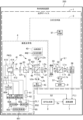
図1は、第1実施形態に係る分光装置100を示す概略構成図である。図2は、図1の分析光学系3、測長光学系4、信号生成部8および演算装置7の各主要部を示す模式図である。
Figure 1 is a schematic diagram showing the configuration of a
1.1.分光装置
図1に示す分光装置100では、入射された分析光L1を被検体である試料9に照射させ、試料9から放射された分析光L1をマイケルソン型干渉光学系に通し、得られた干渉光の強度変化を検出し、後述する演算を行うことにより、インターフェログラムを取得する。取得したインターフェログラムをフーリエ変換することにより、試料9に由来する情報を含むスペクトルパターンが得られる。分析光L1の波長を選択することにより、図1に示す分光装置100は、例えば試料9に対するFT-IR(フーリエ型赤外分光分析)、FT-NIR(フーリエ型近赤外分光分析)、FT-VIS(フーリエ型可視分光分析)、FT-UV(フーリエ型紫外分光分析)、FT-THz(フーリエ型テラヘルツ分光分析)等に適用可能である。
1, the
分光装置100は、光学デバイス1と、信号生成部8と、演算装置7と、を備える。
このうち、光学デバイス1は、図1に示すように、分析光学系3および測長光学系4を備える。
The
As shown in FIG. 1, the optical device 1 includes an analysis
分析光学系3は、分析光L1を試料9に照射するとともに、分析光L1から試料9に由来する試料由来信号を取り出せるように、分析光L1の光路長を変化させながら、分析光L1の分割および混合を行い、干渉を生じさせる。測長光学系4では、レーザー光である測長光L2を用いて、分析光L1の光路長の変化を測定する。
The analytical
信号生成部8は、演算装置7に向けて基準信号Ssを出力する。演算装置7は、分析光学系3から出力された干渉光の強度を表す信号および測長光学系4から出力された光路長の変化を表す信号に基づいて、光路長に対する干渉光の強度を表す波形、すなわち前述したインターフェログラムを求める。また、演算装置7は、インターフェログラムにフーリエ変換を行い、スペクトルパターンを取得する。
The
1.2.光学デバイス
次に、光学デバイス1について説明する。光学デバイス1は、前述したように、分析光学系3、および、測長光学系4を備える。
1.2 Optical Device Next, a description will be given of the optical device 1. As described above, the optical device 1 includes the analysis
1.2.1.分析光学系
分析光学系3は、第1光源51、ビームスプリッター54、集光レンズ55および減光フィルター56を備える。なお、分析光学系3では、これらの光学要素の一部が省略されていてもよいし、これら以外の光学要素を備えていてもよいし、これらの光学要素が他の光学要素で置換されていてもよい。
The analytical
第1光源51は、例えば白色光、すなわち幅広い波長の光が集まった光を分析光L1として射出する光源である。分析光L1の波長域、つまり第1光源51の種類は、試料9に対して行う分光分析の目的に応じて適宜選択される。赤外分光分析を行う場合には、第1光源51としては、例えば、ハロゲンランプ、赤外ランプ、タングステンランプ等が挙げられる。可視光分光分析を行う場合には、第1光源51としては、例えば、ハロゲンランプ等が挙げられる。紫外分光分析を行う場合には、第1光源51としては、例えば、重水素ランプ、UV-LED(紫外線発光ダイオード)等が挙げられる。
The
なお、分析光L1の波長として100nm以上760nm未満を選択することにより、紫外分光分析または可視光分光分析を行い得る分光装置100を実現することができる。また、分析光L1の波長として760nm以上20μm以下を選択することにより、赤外分光分析または近赤外分光分析を行い得る分光装置100を実現することができる。さらに、分析光L1の波長として30μm以上3mm以下を選択することにより、テラヘルツ波分光分析を行い得る分光装置100を実現することができる。
By selecting a wavelength of 100 nm or more and less than 760 nm for the analytical light L1, a
なお、第1光源51は、光学デバイス1に含まれず、外部に設けられていてもよい。この場合、外部に設けられた第1光源51から射出された分析光L1が、光学デバイス1に導入されるようになっていればよい。一方、本実施形態のように、光学デバイス1が第1光源51を備えることにより、第1光源51とビームスプリッター54とのアライメント精度を特に高めることができ、アライメント不良に伴う分析光L1の損失を最小限に抑えることができる。
The
分析光L1は、ビームスプリッター54を透過し、集光レンズ55で集光されて、試料9に照射される。
The analytical light L1 passes through the
ビームスプリッター54には、例えば、無偏光ビームスプリッターが用いられるが、偏光ビームスプリッターが用いられてもよい。この場合、必要な波長板を適宜追加すればよい。なお、第1光源51から射出された分析光L1のうち、一部は、ビームスプリッター54で反射するが、本実施形態では、この反射した分析光L1は、用いられることなく放置される。
For example, a non-polarizing beam splitter is used as the
集光レンズ55は、分析光L1を集光させ、試料9に照射される分析光L1のスポットサイズを小さくする。これにより、局所分析が可能になる。
The focusing
試料9から射出された分析光L1は、試料9との作用により生成された試料由来信号を含んでいる。試料由来信号とは、例えば、分析光L1が試料9に作用したときの、試料9による特定波長の光吸収等が挙げられる。この分析光L1は、集光レンズ55を経て、ビームスプリッター54で反射され、減光フィルター56を通過する。減光フィルター56は、所定波長の光を選択的に減衰させる。これにより、試料由来信号のS/N比(信号対雑音比)を高めることができ、分光分析をより精度よく行うことができる。減光フィルター56としては、例えば、光学濃度(OD値)が6.0以上のノッチフィルター等が挙げられる。
The analytical light L1 emitted from the
また、分析光学系3は、マイケルソン型干渉光学系を構成する、ビームスプリッター32、移動ミラー33、固定ミラー34、集光レンズ35および第1受光素子36を備える。なお、分析光学系3では、これらの光学要素の一部が省略されていてもよいし、これら以外の光学要素を備えていてもよいし、これらの光学要素が他の光学要素で置換されていてもよい。
The analytical
ビームスプリッター32は、分析光L1を2つの分析光L1a、L1bに分割する無偏光ビームスプリッターである。具体的には、ビームスプリッター32は、分析光L1の一部を分析光L1aとして移動ミラー33に向けて反射させ、分析光L1の他部を分析光L1bとして固定ミラー34に向けて透過させることにより、分析光L1を2つに分割する。
The
ビームスプリッター32の種類としては、例えば、図1に示すプリズム型素子(キューブ型素子)の他、プレート型素子、積層型素子等が挙げられる。プレート型のビームスプリッター32を用いた場合には、分析光L1aと分析光L1bとで波長分散が生じるので、必要に応じて、ビームスプリッター32と固定ミラー34との間に、波長分散補償板を配置するようにしてもよい。波長分散補償板は、硝材の光路長差による波長分散を補償する光学要素である。本実施形態では、ビームスプリッター32としてプリズム型素子が用いられているので、この波長分散補償板は不要である。プリズム型素子は、プリズム同士の間に光学薄膜が挟まれた形態の素子である。また、積層型素子は、2枚の透明平板の間に光学薄膜が挟まれた形態の素子である。積層型素子でも、プリズム型素子と同様、波長分散補償板を不要にできる。また、プリズム型素子や積層型素子では、光学薄膜が露出しないので、ビームスプリッター32の長期信頼性を高めることができる。
The types of the
また、ビームスプリッター32は、移動ミラー33で反射された分析光L1aを第1受光素子36に向けて透過させ、固定ミラー34で反射された分析光L1bを第1受光素子36に向けて反射させる。したがって、ビームスプリッター32は、分割された分析光L1a、L1bを混合する。
The
移動ミラー33は、ビームスプリッター32に対して分析光L1aの入射方向に移動し、かつ、分析光L1aを反射させる鏡である。移動ミラー33で反射した分析光L1aは、移動ミラー33の位置に応じて位相が変化する。これにより、移動ミラー33は、分析光L1aに第1変調信号を付加する。第1変調信号は、移動ミラー33の位置に応じて分析光L1aに付加される位相の変化である。
The
移動ミラー33を移動させる図示しない移動機構としては、特に限定されないが、例えば、1軸リニアステージ、ピエゾ駆動装置、MEMS(Micro Electro Mechanical Systems)技術を用いたマイクロアクチュエーター等が挙げられる。このうち、1軸リニアステージは、例えば、ボイスコイルモーター(VCM)またはボールねじ駆動部とリニアガイド機構とを備えることで、移動ミラー33の移動において良好な並進性を実現することができる。
The moving mechanism (not shown) that moves the moving
固定ミラー34は、ビームスプリッター32に対して位置が固定され、分析光L1bを反射させる鏡である。固定ミラー34で反射した分析光L1bは、ビームスプリッター32で分析光L1aと混合され、干渉光として第1受光素子36で受光される。分析光学系3では、移動ミラー33の位置に応じて、分析光L1aの光路と、分析光L1bの光路と、の間に光路差が生じる。このため、干渉光の強度は、移動ミラー33の位置に応じて変化する。
The fixed
移動ミラー33および固定ミラー34は、それぞれ平板ミラーであってもよいし、コーナーキューブミラーであってもよい。各ミラーの反射面には、Al、Au、Agのような金属を用いたメタルコート、誘電体多層膜等が成膜されていてもよい。また、移動ミラー33について、「分析光の入射方向に移動」は、分析光の入射方向の成分を含む方向に移動することを含む。したがって、移動ミラー33は、入射方向に対して斜めに傾いた方向(非平行な方向)に移動してもよい。その場合、演算装置7は、移動ミラー33が分析光の入射方向に対して斜めに傾いた影響を除去する機能を有していればよい。さらに、固定ミラー34も移動するように構成されていてもよい。その場合、演算装置7は、固定ミラー34が移動した影響を除去する機能を有していればよい。
The
集光レンズ35は、干渉光、すなわち混合された分析光L1a、L1bを第1受光素子36に集光させる。
The focusing
第1受光素子36は、干渉光を受光し、その強度を取得する。そして、強度の時間変化を示す信号を第1受光信号F(t)として出力する。この第1受光信号F(t)は、分析光L1と試料9との相互作用により生成された試料由来信号と、前述した第1変調信号と、を含む。
The first
第1受光素子36としては、例えば、フォトダイオード、フォトトランジスタ等が挙げられる。このうち、フォトダイオードとしては、例えば、InGaAs系フォトダイオード、Si系フォトダイオード、アバランシェ型フォトダイオード等が挙げられる。
Examples of the first
1.2.2.測長光学系
測長光学系4は、マイケルソン型干渉光学系であり、第2光源41と、測長部40と、ガスセル61と、射出光量検出部62と、光源制御部65と、を備える。なお、測長光学系4では、これらの光学要素の一部が省略されていてもよいし、これら以外の光学要素を備えていてもよいし、これらの光学要素が他の光学要素で置換されていてもよい。
1.2.2. Length measurement optical system The length measurement
第2光源41は、スペクトル線幅の狭い光を射出する光源が好ましく用いられる。第2光源41としては、例えば、He-Neレーザー、Arレーザーのようなガスレーザー、DFB-LD(Distributed FeedBack - Laser Diode:分布帰還型レーザーダイオード)、FBG-LD(Fiber Bragg Grating - Laser Diode:ファイバーブラッググレーティング付きレーザーダイオード)、VCSEL(Vertical Cavity Surface Emitting Laser:垂直共振器面発光レーザーダイオード)、FP-LD(Fabry-Perot Laser Diode:ファブリーペロー型半導体レーザーダイオード)のような半導体レーザー素子、YAG(Yttrium Aluminum Garnet)のような結晶レーザー等が挙げられる。
The second
第2光源41は、特に半導体レーザー素子であるのが好ましい。これにより、光学デバイス1および分光装置100の小型化および軽量化を図ることができる。
The second
また、図1に示す第2光源41は、発光素子410および温調素子412を備える。
本実施形態では、発光素子410が半導体レーザー素子である。
The second
In this embodiment, the
温調素子412は、例えば、ペルチェ素子、ヒーター等で構成される。温調素子412が発熱または吸熱することにより、第2光源41が有する発光素子410の温度を調整することができる。なお、以下の説明では、発光素子410の温度を「第2光源41の温度」ということもある。
The
測長光学系4は、さらに、ビームスプリッター63およびコリメートレンズ64を備える。
The length measurement
コリメートレンズ64は、第2光源41とビームスプリッター63との間に設けられ、第2光源41から射出された測長光L2を平行化する。なお、測長光L2が射出時点で十分に平行化されている場合には、コリメートレンズ64が省略されていてもよい。
The collimating
ビームスプリッター63は、例えば無偏光ビームスプリッターである。ビームスプリッター63は、測長光L2に分岐させ、測長光L2cを生成する。また、ビームスプリッター63は、測長光L2の残部を透過させて、測長部40に入射させる。分岐比は、特に限定されないが、反射光よりも透過光の光量が多くなるように、具体的には反射光の比率が10%以下程度になるように設定されているのが好ましい。
The
1.2.2.1.測長部
測長部40は、第2光分割素子42、光帰還部43、および、第2受光素子45を備える。
1.2.2.1. Length Measuring Unit The
第2光分割素子42は、ビームスプリッター422、1/2波長板46、1/4波長板47、1/4波長板48、および、検光子49を備える。
The second
ビームスプリッター422は、P偏光を透過させ、S偏光を反射させる偏光ビームスプリッターである。1/2波長板46は、その光学軸が、測長光L2の偏光軸に対して回転した状態で配置されている。これにより、測長光L2は、1/2波長板46を通過することにより、P偏光とS偏光とを含む直線偏光になり、ビームスプリッター422でP偏光とS偏光の2つに分割される。
S偏光である測長光L2aは、1/4波長板48で円偏光に変換され、光帰還部43に入射する。光帰還部43は、測長光L2aを反射させることにより、ビームスプリッター422に帰還させる。このとき、測長光L2aは、1/4波長板48でP偏光に変換される。
The measurement light L2a, which is S-polarized light, is converted to circularly polarized light by the quarter-
一方、P偏光である測長光L2bは、1/4波長板47で円偏光に変換され、移動ミラー33に入射する。移動ミラー33は、測長光L2bを反射させる。これにより、測長光L2bは、移動ミラー33の位置に応じて位相が変化する。その結果、移動ミラー33は、測長光L2bに変位信号を付加する。移動ミラー33で反射した測長光L2bは、ビームスプリッター422に戻る。このとき、測長光L2bは、1/4波長板47でS偏光に変換される。
On the other hand, the P-polarized measurement light L2b is converted to circularly polarized light by the quarter-
なお、図1に示す測長光学系4は、前述した分析光学系3において分析光L1aが入射する移動ミラー33の面とは異なる面に、測長光L2bが入射するように構成されているが、測長光L2bは、分析光L1aが入射する面と同じ面に入射するようになっていてもよい。
The length measurement
また、ビームスプリッター422は、光帰還部43から帰還した測長光L2aを第2受光素子45に向けて透過させ、移動ミラー33で反射された測長光L2bを第2受光素子45に向けて反射させる。したがって、ビームスプリッター422は、分割された測長光L2a、L2bを混合する。混合された測長光L2a、L2bは、検光子49を透過し、第2受光素子45に入射する。
The
なお、ビームスプリッター422には、偏光ビームスプリッターに代えて無偏光ビームスプリッターを用いるようにしてもよい。この場合、波長板等が不要となるため、部品点数の削減による光学デバイス1の小型化を図ることができる。
In addition, a non-polarized beam splitter may be used for the
光帰還部43は、光反射器442を備え、ビームスプリッター422で反射されて入射された光を反射させ、ビームスプリッター422に帰還させる。光反射器442は、例えばミラーで構成される。これにより、光帰還部43の構成を簡素化でき、光学デバイス1の小型化に寄与できる。
The
第2受光素子45は、混合された測長光L2a、L2bを干渉光として受光し、その強度を取得する。そして、強度の時間変化を示す信号を第2受光信号S2として出力する。この第2受光信号S2は、移動ミラー33の変位信号を含む信号である。変位信号は、移動ミラー33の位置に応じて測長光L2bに付加される位相の変化である。以上のようにして、測長部40は、移動ミラー33の位置を示す変位信号を取得する。
The second
第2受光素子45としては、例えば、フォトダイオード、フォトトランジスタ等が挙げられる。
Examples of the second
1.2.2.2.ガスセル
ガスセル61には、所定の波長の光を吸収するガスが封入されている。ガスセル61に測長光L2cが入射されると、測長光L2cに光吸収信号が付加される。光吸収信号は、ガスによる特定波長の光吸収である。
1.2.2.2 Gas Cell The
ガスセル61に封入されるガスとしては、ガス状のセシウム、ルビジウムのようなアルカリ金属、ガス状のヨウ素のようなハロゲン、クリプトンのような希ガスの他、シアン化水素、アセチレン等が挙げられる。これらの原子または分子は、所定の波長の光を吸収したり、放出したりする。ガスセル61には、図示しない温度調整機構が設けられていてもよい。これにより、ガスセル61をより小型化してもガスの蒸気圧を十分に高められる。その結果、ガスセル61の小型化を図ることができる。
Gases that may be filled into the
ガスセル61に封入されるガス(原子または分子)と、そのガスに照射される光の波長の組み合わせ例を下記表1に示す。
Table 1 below shows examples of combinations of the gas (atoms or molecules) sealed in the

ビームスプリッター63で分岐した測長光L2cは、ガスセル61に入射される。そして、ガスセル61に封入されているガスに測長光L2cが照射される。これにより、ガスを構成する原子や分子は、測長光L2cのエネルギーに応じて、基底状態からエネルギーがより高い状態(励起状態)に遷移する。
The measurement light L2c split by the
図3は、セシウム原子の基底状態の超微細構造を示すエネルギー準位図である。
セシウム原子は、図3に示すように、基底準位として6S1/2で表されるエネルギー準位と、励起準位として6P1/2で表されるエネルギー準位と、を有することが知られている。また、6S1/2および6P1/2の各エネルギー準位は、複数のエネルギー準位に分裂した超微細構造を有している。具体的には、6S1/2は、F=3およびF=4で表される2つの基底準位を持っている。また、6P1/2は、F’=3およびF’=4で表される2つの励起準位を持っている。
FIG. 3 is an energy level diagram showing the hyperfine structure of the ground state of the cesium atom.
As shown in Figure 3, it is known that the cesium atom has an energy level represented by 6S 1/2 as the ground level and an energy level represented by 6P 1/2 as the excited level. Each of the energy levels of 6S 1/2 and 6P 1/2 has a hyperfine structure split into multiple energy levels. Specifically, 6S 1/2 has two ground levels represented by F=3 and F=4. Also, 6P 1/2 has two excited levels represented by F'=3 and F'=4.
基底準位にあるセシウム原子は、図3に示すCs(D1)線を吸収することで、励起準位に遷移する。 A cesium atom in the ground level transitions to an excited level by absorbing the Cs (D1) line shown in Figure 3.
例えば、F=4の基底準位にあるセシウム原子は、図3に矢印(1)で示す準位間のエネルギーを吸収することにより、F’=3の励起準位に遷移する。また、図3に矢印(2)で示す準位間のエネルギーを吸収することにより、F’=4の励起準位に遷移する。 For example, a cesium atom in the ground level of F=4 transitions to an excited level of F'=3 by absorbing energy between levels as shown by arrow (1) in Figure 3. Also, by absorbing energy between levels as shown by arrow (2) in Figure 3, it transitions to an excited level of F'=4.
また、F=3の基底準位あるセシウム原子は、図3に矢印(3)で示す準位間のエネルギーを吸収することにより、F’=3の励起準位に遷移する。また、図3に矢印(4)で示す準位間のエネルギーを吸収することにより、F’=4の励起準位に遷移する。
図3の各矢印(1)~(4)の遷移に対応する共鳴波長を、下記表2に示す。
A cesium atom in the ground level of F=3 transitions to an excited level of F'=3 by absorbing energy between levels indicated by arrow (3) in Fig. 3. A cesium atom in the ground level of F=3 transitions to an excited level of F'=3 by absorbing energy between levels indicated by arrow (4) in Fig. 3.
The resonance wavelengths corresponding to the transitions of the arrows (1) to (4) in FIG.

図4は、図3に示すCs(D1)線の吸収スペクトルAS1である。図4に示す吸収スペクトルAS1には、4本の吸収ピークP1~P4が認められる。この吸収ピークP1~P4の周波数は、図3に矢印(1)~(4)で表された4つの遷移周波数に対応している。 Figure 4 shows the absorption spectrum AS1 of the Cs (D1) line shown in Figure 3. Four absorption peaks P1 to P4 can be seen in the absorption spectrum AS1 shown in Figure 4. The frequencies of these absorption peaks P1 to P4 correspond to the four transition frequencies indicated by arrows (1) to (4) in Figure 3.
後述するように、光源制御部65では、第2光源41に入力するバイアス電流を調整する。バイアス電流が変更されると、それに応じて、第2光源41から射出される測長光L2の光量が変化するとともに、中心波長(中心周波数)が変化する。したがって、測長光L2cをガスセル61に入射し、ガスセル61から射出された光の光量変化を観測すると、図5に示すような吸収スペクトルAS2が得られる。
As described below, the light
図5は、第2光源41に入力されるバイアス電流と、ガスセル61から射出された光の光量と、の関係を示す吸収スペクトルAS2である。図5の横軸は、第2光源41に入力されるバイアス電流であり、縦軸は、ガスセル61から射出された光の光量である。バイアス電流が大きくなると、第2光源41から射出される測長光L2の中心波長は長く、中心周波数は小さくなるため、図5では、横軸に付した矢印の向きでそれを表している。
Figure 5 shows an absorption spectrum AS2 that indicates the relationship between the bias current input to the second
図5に示すように、バイアス電流を大きくすると、ガスセル61から射出される光の光量も大きくなる。このため、図5に示す吸収スペクトルAS2は、基本的に単調増加のスペクトルとなる。一方、第2光源41では、バイアス電流に応じて測長光L2の中心波長も変化する。このため、バイアス電流が変化する過程で、測長光L2cの中心波長(中心周波数)と前述した4つの遷移周波数とが一致するとき、ガスセル61から射出される光の光量がそれぞれ極小値をとる。そこで、後述する光源制御部65は、ガスセル61から射出される光の光量が、この4つの吸収ピークP1~P4のいずれかに対応する極小値をとるように、バイアス電流を調整する。その結果、第2光源41から射出される測長光L2の中心波長を安定させることができる。なお、吸収ピークP1~P4の周波数は、ガスセル61に封入されている原子や分子の準位間のエネルギーに対応しており、精度および安定性が極めて高い。このため、測長光L2の中心波長を高い精度で安定させることができる。
As shown in FIG. 5, when the bias current is increased, the amount of light emitted from the
なお、図5において、いずれの吸収ピークが選択されてもよいが、バイアス電流が最も大きい吸収ピークが好ましく選択される。これにより、第2光源41の光出力が最も大きくなるため、第2受光素子45に入射する干渉光の光量を最大化することができる。その結果、第2受光信号S2のS/N比(信号対雑音比)を高めることができる。また、図5では、吸収ピークP1~P4が互いに分解されているが、これらは互いに分解されずに1つのピークとして観測されてもよい。この場合、図3に示すCs(D1)線の波長894.593nmにピークをとることになるため、この波長を利用してもよい。
In FIG. 5, any absorption peak may be selected, but the absorption peak with the largest bias current is preferably selected. This maximizes the optical output of the second
以上、各光学系が備える光学要素について説明したが、光を入射させる必要がある光学要素については、反射防止処理が施されているのが好ましい。これにより、第1受光信号F(t)および第2受光信号S2のS/N比を高めることができる。 The optical elements of each optical system have been described above, but it is preferable that the optical elements into which light must be incident are subjected to anti-reflection treatment. This can increase the S/N ratio of the first light receiving signal F(t) and the second light receiving signal S2.
1.2.2.3.射出光量検出部
射出光量検出部62は、ガスセル61から射出された光の光量を検出する。そして、光量に応じた射出光量検出信号SL1を出力する。射出光量検出部62としては、例えば、フォトダイオード、フォトトランジスタ等が挙げられる。
The emitted light
1.2.2.4.光源制御部
光源制御部65は、射出光量検出信号SL1に基づいて、第2光源41から射出される測長光L2の波長を制御する。
1.2.2.4. Light Source Controller The
図1に示す光源制御部65は、低周波発振器651、検波回路652、変調回路653、光源駆動回路654および温調素子駆動回路655を有する。
The light
低周波発振器651は、例えば、数Hz~数百Hz程度の低い周波数で発振し、低周波信号を出力する。
The low-
検波回路652には、射出光量検出信号SL1が入力される。射出光量検出信号SL1は、後述する変調回路653でバイアス電流に変調が印加されているため、低周波信号の振幅によって決まる範囲でバイアス電流が掃引された結果を含んでいる。つまり、測長光L2の波長(周波数)が所定の範囲で振動し、それに応じた射出光量の変化の振動を含んでいる。このため、検波回路652では、バイアス電流と射出光量との関係が得られることになり、図6に示す吸収スペクトルAS3が得られる。
The
図6は、第2光源41に入力されるバイアス電流と、射出光量検出信号SL1の電圧と、の関係を示す吸収スペクトルAS3、および、吸収スペクトルAS3の一次微分である誤差信号ESの波形を示す図である。
Figure 6 shows an absorption spectrum AS3 that indicates the relationship between the bias current input to the second
図6の吸収スペクトルAS3の横軸は、第2光源41に入力されるバイアス電流であり、縦軸は、電圧信号である射出光量検出信号SL1である。また、図6の誤差信号ESは、吸収スペクトルAS3を微分することによって生成される。誤差信号ESの波形の横軸は、第2光源41に入力されるバイアス電流であり、縦軸は、誤差信号ESの電圧である。
The horizontal axis of the absorption spectrum AS3 in FIG. 6 is the bias current input to the second
誤差信号ESは、図6に示すように、吸収スペクトルAS3の吸収ピークに対応したゼロクロス点を持ち、その前後では、誤差信号が単調に変化している。このため、図1に示す光源駆動回路654では、この吸収ピークに対応する誤差信号ESに基づいて、ガスセル61から射出される光の光量が極小値をとるようにバイアス電流を調整できる。これにより、第2光源41から射出される測長光L2の中心波長(中心周波数)は、吸収ピークP1~P4のいずれかの周波数にロックされ、安定する。
As shown in FIG. 6, the error signal ES has a zero-crossing point corresponding to the absorption peak of the absorption spectrum AS3, and the error signal changes monotonically before and after this point. Therefore, in the light
以上のように、検波回路652は、低周波信号を用いてその周波数で、射出光量検出信号SL1を同期検波する。これにより、図6に示す誤差信号ESを生成し、出力する。
As described above, the
変調回路653は、低周波信号を用いて誤差信号ESに変調を印加する。そして、変調が印加された誤差信号ESを出力する。
The
光源駆動回路654は、変調が印加された誤差信号ESを用いて、第2光源41に入力されるバイアス電流を調整する。例えば、誤差信号ESの電圧が正であれば、バイアス電流を減少させ、誤差信号ESの電圧が負であれば、バイアス電流を増加させる。また、光源駆動回路654は、バイアス電流を所定の幅で掃引する。以上の動作により、ガスセル61から射出される光の光量が極小値からずれても、そのずれがバイアス電流にフィードバックされ、極小値に近づくように調整される。その結果、測長光L2の中心波長(中心周波数)が吸収ピークP1~P4のいずれかのピークトップにロックされ、安定する。
The light
なお、吸収ピークP1~P4は、ガスセル61に封入されている原子や分子の動きに伴うドップラー拡がりを持つ。ドップラー拡がりは、例えばセシウム原子の場合、60℃で380MHz程度になる。測長光L2の中心波長をピークトップにロックするためには、変調の周波数幅をドップラー拡がりより小さくしておくのが好ましい。つまり、バイアス電流の変調幅は、変調の周波数幅がドップラー拡がり未満になるように設定されるのが好ましい。また、より安定して動作させることを考慮すれば、ドップラー拡がりの1/2以下に設定するのが好ましく、1/3以下に設定するのがより好ましい。一方、下限値は、フィードバック制御が安定するように適宜設定されるが、一例としてドップラー拡がりの1/20以上とされる。
The absorption peaks P1 to P4 have Doppler broadening due to the movement of atoms and molecules sealed in the
図7は、以上で説明したバイアス電流のフィードバック制御を説明するためのフローチャートである。 Figure 7 is a flowchart to explain the feedback control of the bias current described above.
図7に示すステップS102では、バイアス電流を掃引し、吸収スペクトルAS3を観測する。 In step S102 shown in FIG. 7, the bias current is swept and the absorption spectrum AS3 is observed.
ステップS104では、所望の吸収ピークを検出し、バイアス電流の値を設定する。
ステップS106では、レーザー光源である第2光源41の電流変調の同期検波により、誤差信号ESを観測する。
In step S104, a desired absorption peak is detected and the value of the bias current is set.
In step S106, the error signal ES is observed by synchronous detection of the current modulation of the second
ステップS108では、誤差信号ESの電圧が正であるか否かを判定する。正である場合、ステップS110に移行する。ステップS110では、バイアス電流を減少させる方向に調整する。一方、負である場合、ステップS112に移行する。ステップS112では、バイアス電流を増加させる方向に調整する。 In step S108, it is determined whether the voltage of the error signal ES is positive. If it is positive, the process proceeds to step S110. In step S110, the bias current is adjusted to decrease. On the other hand, if it is negative, the process proceeds to step S112. In step S112, the bias current is adjusted to increase.
ステップS114では、誤差信号ESの電圧がゼロ近傍に収束したか否かを判定する。収束していない場合、ステップS106に戻る。収束していた場合、フローを終了する。 In step S114, it is determined whether the voltage of the error signal ES has converged to near zero. If it has not converged, the process returns to step S106. If it has converged, the flow ends.
そして、必要に応じて、以上のフローを繰り返す。これにより、測長光L2の中心波長(中心周波数)を安定させることができる。このようなバイアス電流のフィードバック制御は、中心波長の安定化におけるレスポンスが比較的高く、測長光L2の中心波長の高安定化に寄与するという点で有用である。 The above flow is then repeated as necessary. This allows the central wavelength (central frequency) of the measurement light L2 to be stabilized. Such feedback control of the bias current is useful in that it has a relatively high response in stabilizing the central wavelength and contributes to high stabilization of the central wavelength of the measurement light L2.
なお、上記のフィードバック制御は、常時実行されるようになっていてもよいし、必要に応じて随時実行されるようになっていてもよい。例えば、移動ミラー33に対する計測を行う場合には、フィードバック制御を停止するようになっていてもよい。これにより、フィードバック制御が計測精度に影響するのを避けることができる。
The above feedback control may be performed continuously or whenever necessary. For example, when performing measurements on the moving
温調素子駆動回路655は、温調素子412に対し、温度調整信号を出力する。これにより、温調素子412の発熱または吸熱を調整し、第2光源41の温度を目的とする温度に制御する。図1に示す温調素子駆動回路655は、第2光源41の温度を好ましくは一定値に固定するようになっている。これにより、光源駆動回路654の動作が阻害されるのを防止できる。なお、本実施形態において、温調素子412および温調素子駆動回路655は、省略されていてもよい。
The temperature control
1.3.信号生成部
図2に示す信号生成部8は、周期信号を生成し、基準信号Ssとして出力する。信号生成部8としては、例えば、ファンクションジェネレーター、シグナルジェネレーター、数値制御型信号発生器等が挙げられる。後述する演算装置7では、基準信号Ssおよび前述した変位信号に基づいて、移動ミラー位置信号X(t)を生成する。
2 generates a periodic signal and outputs it as a reference signal Ss. Examples of the
1.4.演算装置
図2に示す演算装置7は、移動ミラー位置演算部72、光強度演算部74およびフーリエ変換部76を有する。これらの機能部が発揮する機能は、例えば、プロセッサー、メモリー、外部インターフェース、入力部、表示部等を備えるハードウェアによって実現される。具体的には、メモリーに格納されているプログラムをプロセッサーが読み出し、実行することによって実現される。なお、これらの構成要素は、外部バスによって互いに通信可能になっている。
1.4. Calculation device The
プロセッサーとしては、例えば、CPU(Central Processing Unit)、DSP(Digital Signal Processor)等が挙げられる。なお、これらのプロセッサーがソフトウェアを実行する方式に代えて、FPGA(Field-Programmable Gate Array)やASIC(Application Specific Integrated Circuit)等が上述した機能を実現する方式を採用するようにしてもよい。 Examples of processors include a CPU (Central Processing Unit) and a DSP (Digital Signal Processor). Note that instead of using these processors to execute software, a system in which an FPGA (Field-Programmable Gate Array) or an ASIC (Application Specific Integrated Circuit) realizes the above-mentioned functions may be adopted.
メモリーとしては、例えば、HDD(Hard Disk Drive)、SSD(Solid State Drive)、EEPROM(Electrically Erasable Programmable Read-Only Memory)、ROM(Read-Only Memory)、RAM(Random Access Memory)等が挙げられる。 Examples of memory include HDD (Hard Disk Drive), SSD (Solid State Drive), EEPROM (Electrically Erasable Programmable Read-Only Memory), ROM (Read-Only Memory), RAM (Random Access Memory), etc.
外部インターフェースとしては、例えば、USB(Universal Serial Bus)等のデジタル入出力ポート、イーサネット(登録商標)ポート等が挙げられる。 External interfaces include, for example, digital input/output ports such as USB (Universal Serial Bus) and Ethernet (registered trademark) ports.
入力部としては、例えば、キーボード、マウス、タッチパネル、タッチパッド等の各種入力装置が挙げられる。表示部としては、例えば、液晶ディスプレイパネル、有機EL(Electro Luminescence)ディスプレイパネル等が挙げられる。なお、入力部および表示部は、必要に応じて設けられればよく、省略されていてもよい。 Examples of the input unit include various input devices such as a keyboard, a mouse, a touch panel, and a touch pad. Examples of the display unit include a liquid crystal display panel and an organic EL (Electro Luminescence) display panel. Note that the input unit and the display unit may be provided as necessary, and may be omitted.
1.4.1.移動ミラー位置演算部
移動ミラー位置演算部72は、信号生成部8から出力された基準信号Ssに基づいて、移動ミラー33の変位信号を含む第2受光信号S2に対して演算を行う。これにより、移動ミラー33の位置を示す移動ミラー位置信号X(t)を生成する。移動ミラー33が移動すると、それに伴って測長光学系4における干渉光の強度が変化する。この場合、第2受光信号S2は、例えば、干渉条件に応じて振幅が周期的に変化する信号となる。第2受光信号S2の振幅の変化から、移動ミラー33の変位を算出することができ、移動ミラー位置信号X(t)が求められる。
1.4.1. Moving mirror position calculation unit The moving mirror
なお、移動ミラー位置信号X(t)によって表される移動ミラー33の計測変位dは、下記式(A)で表される。
The measured displacement d of the moving

上記式(A)のλは、測長光L2の波長であり、nは、雰囲気の屈折率であり、φは、移動ミラー33で反射した測長光L2bの位相である。
In the above formula (A), λ is the wavelength of the measurement light L2, n is the refractive index of the atmosphere, and φ is the phase of the measurement light L2b reflected by the
上記式(A)からわかるように、計測変位dは、測長光L2の波長λの影響を受ける。例えば、経時変化等により、初期の波長λがλ’になった場合を考える。この場合の計測変位をd’とすると、計測変位d’は、下記式(A’)で表される。 As can be seen from the above formula (A), the measured displacement d is affected by the wavelength λ of the measurement light L2. For example, consider a case where the initial wavelength λ becomes λ' due to changes over time. If the measured displacement in this case is d', then the measured displacement d' is expressed by the following formula (A').

ここで、初期の計測変位dが計測変位d’に変化した場合の変化率をΔd/dとする。計測変位の変化率Δd/dは、下記式(B)で表される。 Here, the rate of change when the initial measured displacement d changes to the measured displacement d' is Δd/d. The rate of change of the measured displacement Δd/d is expressed by the following formula (B).

したがって、波長の変化率Δλ/λは、計測変位の変化率Δd/dに影響を及ぼすことがわかる。よって、測長光L2の波長を安定させることができれば、計測変位dの精度を高めることができる。 It can therefore be seen that the rate of change of the wavelength Δλ/λ affects the rate of change of the measured displacement Δd/d. Therefore, if the wavelength of the measurement light L2 can be stabilized, the accuracy of the measured displacement d can be improved.
1.4.2.光強度演算部
光強度演算部74は、第1受光信号F(t)および移動ミラー位置信号X(t)に基づいて、移動ミラー33の位置に対する干渉光の強度を表す波形(インターフェログラムF(x))を生成する。
1.4.2. Light Intensity Calculation Section The light
第1受光信号F(t)は、前述したように、試料由来信号および第1変調信号を含んでいる。光強度演算部74では、移動ミラー位置信号X(t)に基づいて、第1受光信号F(t)の強度を抽出する。そして、光強度演算部74は、移動ミラー位置信号X(t)から求められる移動ミラー33の位置と第1受光信号F(t)の強度とにより、インターフェログラムF(x)を生成する。なお、インターフェログラムF(x)は、分析光学系3における移動ミラー33での反射光と固定ミラー34での反射光との光路差と、第1受光素子36で受光される干渉光の強度(第1受光信号F(t)の強度)と、の関数で表される。
As described above, the first light receiving signal F(t) includes a sample-derived signal and a first modulation signal. The light
図8は、図1に示す光学デバイス1で取得される第1受光信号F(t)および第2受光信号S2の一例を示す図である。図8の横軸は、時刻であり、縦軸は、第1受光素子36に入射する干渉光の強度または第2受光素子45に入射する干渉光の強度である。
Figure 8 is a diagram showing an example of the first light receiving signal F(t) and the second light receiving signal S2 acquired by the optical device 1 shown in Figure 1. The horizontal axis of Figure 8 is time, and the vertical axis is the intensity of the interference light incident on the first
図9は、インターフェログラムF(x)の一例を示す図である。図9の横軸は、分析光学系3の光路差であり、縦軸は、干渉光の強度である。なお、分析光学系3の光路差とは、ビームスプリッター32と移動ミラー33との光路長およびビームスプリッター32と固定ミラー34との光路長の差であり、図9では、光路差ゼロを横軸の原点としている。
Figure 9 shows an example of an interferogram F(x). The horizontal axis of Figure 9 is the optical path difference of the analytical
図10は、図8に示す第2受光信号S2の部分拡大図である。図8に示す第2受光信号S2は、所定の周期で振動する信号であり、振幅が最大になる点が特徴点FPとなる。光強度演算部74は、この特徴点FPの時刻で、図8に示す第1受光信号F(t)の強度を抽出することにより、移動ミラー33の位置と第1受光信号F(t)の強度とを関係づけることができる。これにより、インターフェログラムF(x)のデジタルデータを取得することができる。
Figure 10 is a partially enlarged view of the second light receiving signal S2 shown in Figure 8. The second light receiving signal S2 shown in Figure 8 is a signal that oscillates at a predetermined period, and the point where the amplitude is maximum is the characteristic point FP. The light
なお、測長光L2の波長安定性は、移動ミラー33の位置の精度に直結する。したがって、前述したガスセル61を用いて測長光L2の波長を安定させることにより、インターフェログラムF(x)の横軸である分析光学系3の光路差の精度を高めることができる。
The wavelength stability of the measurement light L2 is directly linked to the positional accuracy of the
1.4.3.フーリエ変換部
フーリエ変換部76は、インターフェログラムF(x)にフーリエ変換を行う。これにより、試料9に固有の情報を含むスペクトルパターンを取得する。
The
図11は、試料9に分光分析を行って得られるスペクトルパターンSP0の一例である。スペクトルパターンSP0は、試料9の反射スペクトルの例である。
Figure 11 shows an example of a spectral pattern SP0 obtained by performing spectroscopic analysis on
図11に示すスペクトルパターンSP0には、分析光L1が試料9に作用して生成された試料由来信号が吸収ピークX9として反映されている。分光装置100によれば、スペクトルパターンSP0に基づいて、試料9の特性、例えば材料、構造、成分量等を分析することができる。
In the spectral pattern SP0 shown in FIG. 11, the sample-derived signal generated by the action of the analytical light L1 on the
このスペクトルパターンSP0は、インターフェログラムF(x)をフーリエ変換して生成されている。インターフェログラムF(x)は、移動ミラー33の位置情報をパラメーターとして得られた電界振幅波形であるから、これをフーリエ変換して得られるスペクトルパターンSP0は、波長情報を持つ。そして、移動ミラー33の位置精度は、スペクトルパターンSP0の波数精度に直結する。よって、本実施形態に係る分光装置100によれば、波長軸(波数軸)の正確度が高いスペクトルパターンSP0を生成可能である。
This spectral pattern SP0 is generated by Fourier transforming the interferogram F(x). Since the interferogram F(x) is an electric field amplitude waveform obtained using the position information of the
また、上記の効果を得るにあたって、第2光源41に半導体レーザー素子のような小型で安価な素子を採用しても、測長光L2の波長安定性を高めることができる。これにより、分光装置100の小型化、軽量化、低消費電力化および低コスト化を図ることができる。
In addition, to obtain the above effects, even if a small and inexpensive element such as a semiconductor laser element is used for the second
2.第1実施形態の第1変形例
次に、第1実施形態の第1変形例に係る分光装置について説明する。
2. First Modification of First Embodiment Next, a spectroscopic device according to a first modification of the first embodiment will be described.
図12は、第1実施形態の第1変形例に係る分光装置100を示す概略構成図である。
以下、第1変形例について説明するが、以下の説明では、前記第1実施形態との相違点を中心に説明し、同様の事項についてはその説明を省略する。なお、図12において、前記第1実施形態と同様の事項については、同一の符号を付している。
FIG. 12 is a schematic diagram showing the configuration of a
The first modification will be described below, focusing on the differences from the first embodiment, and not describing the similarities. Note that in FIG. 12, the same reference numerals are used to denote the same elements as in the first embodiment.
図12に示す分光装置100は、光学デバイス1の分析光学系3の構成が異なること以外、図1に示す分光装置100と同様である。
The
図12に示す分析光学系3は、ビームスプリッター54に代えて、ミラー571を備える。ミラー571は、第1光源51から射出された分析光L1の光路を変更する。また、試料9は、第1光源51とミラー571との間に配置されている。これにより、第1光源51から射出された分析光L1は、試料9を透過して、ミラー571に入射することになる。このため、第1変形例で得られるスペクトルパターンは透過スペクトルとなる。
The analytical
以上のような第1変形例においても、第1実施形態と同様の効果が得られる。なお、ミラー571は、必要に応じて設けられればよく、第1光源51や試料9の配置等によっては、省略されていてもよい。
The first modified example described above also provides the same effects as the first embodiment. The
3.第1実施形態の第2変形例
次に、第1実施形態の第2変形例に係る分光装置について説明する。
図13は、第1実施形態の第2変形例に係る分光装置100を示す概略構成図である。
3. Second Modification of First Embodiment Next, a spectroscopic device according to a second modification of the first embodiment will be described.
FIG. 13 is a schematic diagram showing the configuration of a
以下、第2変形例について説明するが、以下の説明では、前記第1実施形態との相違点を中心に説明し、同様の事項についてはその説明を省略する。なお、図13において、前記第1実施形態と同様の事項については、同一の符号を付している。 The second modified example will be described below, but in the following description, the differences from the first embodiment will be mainly described, and the description of similar matters will be omitted. Note that in FIG. 13, the same reference numerals are used for the same matters as in the first embodiment.
図13に示す分光装置100は、光学デバイス1の分析光学系3の構成が異なること以外、図1に示す分光装置100と同様である。
The
図13に示す分析光学系3は、試料9を介して集光レンズ55の反対側に設けられたミラー572を備える。ミラー572は、試料9を透過した分析光L1を反射させ、再び試料9に入射させる。このため、第2変形例で得られるスペクトルパターンは、透過スペクトルとなる。
The analytical
以上のような第2変形例においても、第1実施形態と同様の効果が得られる。
また、図13に示す分析光学系3では、ビームスプリッター54から射出された分析光L1が、試料9を往復して、ビームスプリッター54に戻ることになる。このため、図13に示す分光装置100で得られるスペクトルパターンでは、試料に由来する情報(ピーク)の強度を、図12に示す分光装置100で得られるスペクトルパターンよりも大きくできるため、S/N比を高められる。
In the second modified example as described above, the same effects as those of the first embodiment can be obtained.
13, the analytical light L1 emitted from the
4.第1実施形態の第3変形例
次に、第1実施形態の第3変形例に係る分光装置について説明する。
図14は、第1実施形態の第3変形例に係る分光装置100を示す概略構成図である。
4. Third Modification of First Embodiment Next, a spectroscopic device according to a third modification of the first embodiment will be described.
FIG. 14 is a schematic diagram showing the configuration of a
以下、第3変形例について説明するが、以下の説明では、前記第1実施形態との相違点を中心に説明し、同様の事項についてはその説明を省略する。なお、図14において、前記第1実施形態と同様の事項については、同一の符号を付している。 The third modified example will be described below, but in the following description, the differences from the first embodiment will be mainly described, and the description of similar matters will be omitted. Note that in FIG. 14, the same reference numerals are used for the same matters as in the first embodiment.
第3変形例は、光源制御部65が、バイアス電流の調整に代えて第2光源41の温度の調整を行うように構成されている以外、前記実施形態と同様である。
The third modified example is similar to the above embodiment, except that the light
図14に示す光源制御部65は、変調回路653から出力される信号、つまり変調が印加された誤差信号が、温調素子駆動回路655に入力されるようになっている。一方、図14に示す光源駆動回路654は、バイアス電流を好ましくは一定値に固定するようになっている。これにより、温調素子駆動回路655の動作が阻害されるのを防止できる。
The light
図14に示す温調素子駆動回路655は、変調が印加された誤差信号を用いて、温調素子412に入力される温度調整信号を調整する。例えば、誤差信号の電圧が正であれば、温調素子412に吸熱させて第2光源41の温度を低下させ、誤差信号の電圧が負であれば、温調素子412を発熱させて第2光源41の温度を上昇させる。
The temperature control
図15は、第2光源41の温度と、ガスセル61から射出される光の光量と、の関係を示す吸収スペクトルAS4である。図15の横軸は、第2光源41の温度であり、縦軸は、ガスセル61から射出される光の光量である。第2光源41の温度が高くなると、第2光源41から射出される測長光L2の中心波長は長く、中心周波数は小さくなるため、図15では、横軸に付した矢印の向きでそれを表している。
Figure 15 shows an absorption spectrum AS4 indicating the relationship between the temperature of the second
図15に示すように、第2光源41の温度を高くすると、ガスセル61から射出される光の光量は小さくなる。このため、図15に示す吸収スペクトルAS4は、基本的に単調減少のスペクトルとなる。一方、第2光源41では、温度に応じて測長光L2の中心波長も変化する。このため、温度が変化する過程で、測長光L2cの中心波長(中心周波数)と前述した4つの遷移周波数とが一致するとき、ガスセル61から射出される光の光量がそれぞれ極小値をとる。そこで、図14に示す光源制御部65は、ガスセル61から射出される光の光量が、この4つの吸収ピークのいずれかに対応する極小値をとるように、第2光源41の温度を調整する。その結果、第2光源41から射出される測長光L2の中心波長を安定させることができる。
As shown in FIG. 15, when the temperature of the second
以上の動作により、ガスセル61から射出される光の光量が極小値からずれても、そのずれが第2光源41の温度にフィードバックされ、極小値に近づくように調整される。その結果、測長光L2の中心波長(中心周波数)が吸収ピークP1~P4のいずれかのピークトップにロックされ、安定する。
By the above operation, even if the amount of light emitted from the
図16は、以上で説明した第2光源41の温度のフィードバック制御を説明するためのフローチャートである。
Figure 16 is a flowchart for explaining the feedback control of the temperature of the second
図16に示すステップS202では、レーザー光源である第2光源41の温度を掃引し、吸収スペクトルを観測する。
In step S202 shown in FIG. 16, the temperature of the second
ステップS204では、所望の吸収ピークを検出し、第2光源41の温度の値を設定する。
In step S204, the desired absorption peak is detected and the temperature value of the second
ステップS206では、第2光源41の温度変調の同期検波により、誤差信号を観測する。
In step S206, the error signal is observed by synchronous detection of the temperature modulation of the second
ステップS208では、誤差信号の電圧が正であるか否かを判定する。正である場合、ステップS210に移行する。ステップS210では、第2光源41の温度を低下させる方向に調整する。一方、負である場合、ステップS212に移行する。ステップS212では、第2光源41の温度を上昇させる方向に調整する。
In step S208, it is determined whether the voltage of the error signal is positive. If it is positive, the process proceeds to step S210. In step S210, the temperature of the second
ステップS214では、誤差信号の電圧がゼロ近傍に収束したか否かを判定する。収束していない場合、ステップS206に戻る。収束していた場合、フローを終了する。 In step S214, it is determined whether the voltage of the error signal has converged to near zero. If it has not converged, the process returns to step S206. If it has converged, the flow ends.
そして、必要に応じて、以上のフローを繰り返す。これにより、測長光L2の中心波長(中心周波数)を安定させることができる。 Then, the above flow is repeated as necessary. This makes it possible to stabilize the central wavelength (central frequency) of the measurement light L2.
以上のような第3変形例においても、前記第1実施形態と同様の効果が得られる。
また、第3変形例では、測長光L2の波長を所定量調整するときの光量の変化量を、前記第1実施形態に比べて抑えることができる。これにより、前記第1実施形態に比べて、第2受光素子45に入射する干渉光の光量の変化を抑えることができる。その結果、第2受光信号S2のS/N比(信号対雑音比)の経時的な変動を抑制することができる。
In the third modified example as described above, the same effects as those of the first embodiment can be obtained.
In addition, in the third modified example, the change in the light amount when adjusting the wavelength of the measurement light L2 by a predetermined amount can be suppressed compared to the first embodiment. This makes it possible to suppress the change in the light amount of the interference light incident on the second
例えば、一般的な面発光レーザー素子を第2光源41として用い、測長光L2の中心波長を0.1nm長くする調整を行う場合を例に考える。下記表3は、この例における電流波長制御(前記実施形態)と、温度波長制御(第3変形例)とで、射出光L1の中心波長を0.1nm長くする調整を行う場合の電流または温度の変化幅と、調整に伴う光量の変化幅と、を示している。
For example, consider a case where a general surface-emitting laser element is used as the second

前記第1実施形態では、バイアス電流を0.38mA大きくする必要があり、それに伴って、測長光L2の光量が11.5%増加する。これに対し、第3変形例では、第2光源41の温度を1.7℃高くする必要があり、それに伴って、測長光L2の光量が0.7%減少する。このように、第3変形例における光量の変化量は、前記第1実施形態の1/10以下に抑えられている。
In the first embodiment, the bias current needs to be increased by 0.38 mA, which increases the amount of measurement light L2 by 11.5%. In contrast, in the third modified example, the temperature of the second
なお、上記計算例は、下記表4に示す面発光レーザー素子の各種パラメーターを用いて計算したものである。 The above calculation example was performed using the various parameters of the surface-emitting laser element shown in Table 4 below.

5.第1実施形態の第4変形例
次に、第1実施形態の第4変形例に係る分光装置について説明する。
図17は、第1実施形態の第4変形例に係る分光装置100を示す概略構成図である。
5. Fourth Modification of First Embodiment Next, a spectroscopic device according to a fourth modification of the first embodiment will be described.
FIG. 17 is a schematic configuration diagram showing a
以下、第4変形例について説明するが、以下の説明では、前記第3変形例との相違点を中心に説明し、同様の事項についてはその説明を省略する。なお、図17において、前記第3変形例と同様の事項については、同一の符号を付している。 The fourth modified example will be described below, but in the following explanation, the differences from the third modified example will be mainly described, and the explanation of similar matters will be omitted. Note that in FIG. 17, the same reference numerals are used for the same matters as the third modified example.
第4変形例は、光源制御部65が、第2光源41の温度の調整に加え、第2光源41の光出力に基づくバイアス電流の調整を行うように構成されている以外、前記第3変形例と同様である。
The fourth modification is similar to the third modification, except that the light
図17に示す測長光学系4は、さらに、ビームスプリッター66、光出力検出部67およびAPC部656を備える。
The length measurement
ビームスプリッター66は、ビームスプリッター63で分岐された光路に配置される無偏光ビームスプリッターである。ビームスプリッター66は、測長光L2cの一部を反射させて分岐させ、測長光L2dを生成する。また、ビームスプリッター66は、測長光L2cの残部を透過させて、ガスセル61に入射させる。分岐比は、特に限定されない。また、ビームスプリッター66の配置は、上記に限定されない。
The
光出力検出部67は、ビームスプリッター66により分岐された測長光L2dの光量を検出する。本明細書では、この光量を「発光素子410の光出力」という。光出力は、第2光源41から射出された測長光L2の光量に略比例しているので、測長光L2の光量をモニターするために用いられる。光出力検出部67は、測長光L2dの光量に応じた光出力検出信号SL2を出力する。光出力検出部67としては、例えば、フォトダイオード、フォトトランジスタ等が挙げられる。
The optical
APC部656は、光出力検出信号SL2に基づいて、第2光源41の光出力が一定になるようにバイアス電流を制御するための光出力制御信号を出力する。図17に示す光源駆動回路654は、光出力制御信号に基づいてバイアス電流を調整する。APCは、Auto Power Control(自動光量制御)である。
The
以上のように、第4変形例では、第3変形例が有する構成(温度のフィードバック制御)に、APC部656を用いたバイアス電流のフィードバック制御の構成が追加されている。これにより、第2光源41から射出される測長光L2の中心波長(中心周波数)を安定させ、かつ、光出力(光量)を一定に制御することができる。
As described above, in the fourth modified example, a configuration for feedback control of bias current using the
図18は、以上で説明した2つのフィードバック制御(温度とバイアス電流のフィードバック制御)を説明するためのフローチャートである。 Figure 18 is a flowchart to explain the two feedback controls described above (feedback control of temperature and bias current).
図18に示すステップS302では、レーザー光源である第2光源41の温度を掃引し、吸収スペクトルを観測する。
In step S302 shown in FIG. 18, the temperature of the second
ステップS304では、所望の吸収ピークを検出し、第2光源41の温度の値を設定する。
In step S304, the desired absorption peak is detected and the temperature value of the second
ステップS306では、第2光源41の温度変調の同期検波により、誤差信号を観測する。
In step S306, the error signal is observed by synchronous detection of the temperature modulation of the second
ステップS308では、誤差信号の電圧が正であるか否かを判定する。正である場合、ステップS310に移行する。ステップS310では、第2光源41の温度を低下させる方向に調整する。一方、負である場合、ステップS312に移行する。ステップS312では、第2光源41の温度を上昇させる方向に調整する。
In step S308, it is determined whether the voltage of the error signal is positive. If it is positive, the process proceeds to step S310. In step S310, the temperature of the second
ステップS314では、誤差信号の電圧がゼロ近傍に収束したか否かを判定する。収束していない場合、ステップS306に戻る。収束していた場合、ステップS322に移行する。 In step S314, it is determined whether the voltage of the error signal has converged to near zero. If it has not converged, the process returns to step S306. If it has converged, the process proceeds to step S322.
ステップS322では、光出力検出部67から出力される電圧信号である光出力検出信号SL2の電圧値を測定する。なお、電圧値の初期値は、あらかじめ図示しないメモリーに記憶させておく。
In step S322, the voltage value of the optical output detection signal SL2, which is a voltage signal output from the optical
ステップS324では、測定した光出力検出信号SL2の電圧値が初期値より大きいか否かを判定する。大きい場合、ステップS326に移行する。ステップS326では、バイアス電流を減少させる方向に調整する。一方、小さい場合、ステップS328に移行する。ステップS328では、バイアス電流を増加させる方向に調整する。 In step S324, it is determined whether the measured voltage value of the optical output detection signal SL2 is greater than the initial value. If it is greater, the process proceeds to step S326. In step S326, the bias current is adjusted to decrease. On the other hand, if it is smaller, the process proceeds to step S328. In step S328, the bias current is adjusted to increase.
ステップS330では、光出力検出信号SL2の電圧値が初期値近傍に収束したか否かを判定する。収束していない場合、ステップS322に戻る。収束していた場合、フローを終了する。 In step S330, it is determined whether the voltage value of the light output detection signal SL2 has converged to near the initial value. If it has not converged, the process returns to step S322. If it has converged, the flow ends.
そして、必要に応じて、以上のフローを繰り返す。これにより、測長光L2の中心波長(中心周波数)および光出力の双方を安定させることができる。 Then, the above flow is repeated as necessary. This makes it possible to stabilize both the central wavelength (central frequency) and the optical output of the measurement light L2.
6.第1実施形態の第5変形例
次に、第1実施形態の第5変形例に係る分光装置について説明する。
図19は、第1実施形態の第5変形例に係る分光装置100を示す概略構成図である。
6. Fifth Modification of First Embodiment Next, a spectroscopic device according to a fifth modification of the first embodiment will be described.
FIG. 19 is a schematic configuration diagram showing a
以下、第5変形例について説明するが、以下の説明では、前記第4変形例との相違点を中心に説明し、同様の事項についてはその説明を省略する。なお、図19において、前記第4変形例と同様の事項については、同一の符号を付している。 The fifth modified example will be described below, but in the following explanation, the differences from the fourth modified example will be mainly described, and the explanation of similar matters will be omitted. Note that in FIG. 19, the same reference numerals are used for the same matters as the fourth modified example.
第5変形例は、光出力検出部414が、第2光源41が有するパッケージPKG内に設けられていること以外、前記第4変形例と同様である。
The fifth modification is similar to the fourth modification, except that the
図19に示す第2光源41は、さらにパッケージPKGを有する。パッケージPKGは、発光素子410、温調素子412および光出力検出部414を収容する容器である。光出力検出部414は、前述した光出力検出部67と同様、測長光L2dの光量に応じた光出力検出信号SL2を出力する。一方、図19に示す第2光源41では、光出力検出部414がパッケージPKG内に設けられている。これにより、分光装置100のさらなる小型化を図ることができる。
以上のような第5変形例においても、第4変形例と同様の効果が得られる。
The second
In the fifth modified example as described above, the same effects as those of the fourth modified example can be obtained.
7.第1実施形態の第6変形例
次に、第1実施形態の第6変形例に係る分光装置について説明する。
7. Sixth Modification of First Embodiment Next, a spectroscopic device according to a sixth modification of the first embodiment will be described.
図20は、第1実施形態の第6変形例に係る分光装置100を示す概略構成図である。図21は、図20の分析光学系3、測長光学系4、信号生成部8および演算装置7の各主要部を示す模式図である。
Figure 20 is a schematic diagram showing a
以下、第6変形例について説明するが、以下の説明では、前記第1実施形態との相違点を中心に説明し、同様の事項についてはその説明を省略する。なお、図20において、前記第1実施形態と同様の事項については、同一の符号を付している。 The sixth modified example will be described below, but in the following description, the differences from the first embodiment will be mainly described, and the description of similar matters will be omitted. Note that in FIG. 20, the same reference numerals are used for the same matters as in the first embodiment.
第6変形例は、光帰還部43の構成が異なるとともに、低周波発振器651が省略されていること以外、前記第1実施形態と同様である。
The sixth variant is similar to the first embodiment, except that the configuration of the
図20に示す光帰還部43は、光変調器444を備える。光変調器444は、振動素子446を有する。振動素子446は、駆動信号Sdにより振動するとともに、測長光L2aを反射させる。これにより、光変調器444は、測長光L2aに対して第2変調信号を重畳させる。第2変調信号は、測長光L2aが振動素子446で反射されることに伴って生じる周波数の変化である。
The
図20に示す信号生成部8は、発振回路81を有する。発振回路81は、振動素子446が信号源として動作し、精度の高い周期信号を生成する。これにより、発振回路81は、精度の高い駆動信号Sdを出力するとともに、基準信号Ssを出力する。そうすると、駆動信号Sdおよび基準信号Ssは、外乱を受けた場合、互いに同じ影響を受けることになる。その結果、駆動信号Sdにより駆動された振動素子446を介して付加される第2変調信号、および、基準信号Ssも、互いに同じ影響を受ける。このため、第2受光信号S2および基準信号Ssが、演算装置7における演算に供されたとき、演算の過程で、双方が含む外乱の影響を互いに相殺または低減させることができる。その結果、演算装置7では、外乱を受けても、移動ミラー33の位置を精度よく求めることができる。
The
振動素子446としては、例えば、水晶振動子、シリコン振動子、セラミック振動子等が挙げられる。これらの振動子は、共振現象を利用した振動子であるため、Q値が高く、固有振動数の安定化を容易に図ることができる。これにより、光変調器444が測長光L2aに印加する第2変調信号のS/N比を高めることができ、かつ、基準信号Ssの精度を高めることができる。これにより、移動ミラー33の位置を精度よく求めることができ、最終的に、波長軸(波数軸)の正確度が高いスペクトルパターンを生成可能な分光装置100を実現できる。
Examples of the
水晶振動子としては、例えば、水晶AT振動子、SCカット水晶振動子、音叉型水晶振動子、水晶表面弾性波素子等が挙げられる。水晶振動子の発振周波数は、例えば1kHzから数100MHz程度である。 Examples of quartz crystal oscillators include quartz crystal AT oscillators, SC-cut quartz crystal oscillators, tuning fork quartz crystal oscillators, quartz surface acoustic wave elements, etc. The oscillation frequency of a quartz crystal oscillator is, for example, about 1 kHz to several hundred MHz.
シリコン振動子は、単結晶シリコン基板からMEMS技術を用いて製造される単結晶シリコン片と、圧電膜と、を備える振動子である。MEMS(Micro Electro Mechanical Systems)は、微小電気機械システムのことである。単結晶シリコン片の形状としては、例えば、2脚音叉型、3脚音叉型等の片持ち梁形状、両持ち梁形状等が挙げられる。シリコン振動子の発振周波数は、例えば1kHzから数100MHz程度である。 The silicon vibrator is a vibrator that includes a single crystal silicon piece manufactured from a single crystal silicon substrate using MEMS technology, and a piezoelectric film. MEMS (Micro Electro Mechanical Systems) stands for microelectromechanical systems. Examples of the shape of the single crystal silicon piece include cantilever beam shapes such as two-legged tuning fork and three-legged tuning fork, and double-supported beam shapes. The oscillation frequency of the silicon vibrator is, for example, about 1 kHz to several hundred MHz.
セラミック振動子は、圧電セラミックスを焼き固めて製造される圧電セラミック片と、電極と、を備える振動子である。圧電セラミックスとしては、例えば、チタン酸ジルコニウム酸鉛(PZT)、チタン酸バリウム(BTO)等が挙げられる。セラミック振動子の発振周波数は、例えば数100kHzから数10MHz程度である。 A ceramic vibrator is a vibrator that includes a piezoelectric ceramic piece manufactured by baking and hardening piezoelectric ceramics, and electrodes. Examples of piezoelectric ceramics include lead zirconate titanate (PZT) and barium titanate (BTO). The oscillation frequency of a ceramic vibrator is, for example, from several hundred kHz to several tens of MHz.
振動素子446および発振回路81としては、例えば、特開2022-38156号公報に開示されている振動素子および発振回路が挙げられる。
The
図21に示す移動ミラー位置演算部72は、光ヘテロダイン干渉法により、移動ミラー33の位置を特定し、その結果に基づいて、移動ミラー位置信号X(t)を生成する。具体的には、測長光学系4が光変調器444を備えることにより、測長光L2aに第2変調信号を付加することができる。そうすると、測長光L2a、L2bを干渉させたとき、得られた干渉光から移動ミラー33の位置に対応する位相情報をより高い精度で取得することができる。そして、演算装置7において位相情報から移動ミラー33の位置が高精度に求められる。光ヘテロダイン干渉法によれば、位相情報を取り出すとき、外乱の影響、特にノイズとなる周波数の迷光の影響を受けにくく、高いロバスト性が与えられる。
The moving mirror
図21に示す移動ミラー位置演算部72は、前処理部722、復調処理部724、および、移動ミラー位置信号出力部726を有する。前処理部722および復調処理部724には、例えば、特開2022-38156号公報に開示されている前処理部および復調部が適用できる。
The moving mirror
前処理部722は、基準信号Ssに基づいて第2受光信号S2に前処理を行う。復調処理部724は、前処理部722から出力された前処理済み信号から、基準信号Ssに基づいて移動ミラー33の位置に応じた変位信号を復調する。
The
移動ミラー位置信号出力部726は、復調処理部724が復調した移動ミラー33の変位信号に基づいて、移動ミラー位置信号X(t)を生成し、出力する。この方法で求めた移動ミラー位置信号X(t)は、時刻ごとに変化する移動ミラー33の位置を表す信号となる。第2受光信号S2が含む移動ミラー33の変位信号は、測長光L2の波長よりも十分に狭い間隔で移動ミラー33の変位を捉えている。例えば、測長光L2の波長が数100nmである場合、変位信号が示す移動ミラー33の位置分解能としては10nm未満が達成可能になる。これに対し、第1実施形態では、測長光L2の波長の1/4が位置分解能の限界である。このため、光強度演算部74では、第1実施形態に比べてより細かな間隔で、インターフェログラムF(x)のデジタルデータを生成することができる。
The moving mirror position
図22は、図20に示す分光装置100で取得される第1受光信号F(t)および移動ミラー位置信号X(t)の一例を示す図である。図22の横軸は、時刻であり、縦軸は、第1受光素子36に入射する干渉光の強度または移動ミラー33の位置である。
Figure 22 is a diagram showing an example of the first light receiving signal F(t) and the movable mirror position signal X(t) acquired by the
図22に示す移動ミラー位置信号X(t)は、移動ミラー33の位置の変化を、連続的に検出可能な信号になっており、高い位置分解能を実現できている。このため、それに基づいてインターフェログラムF(x)を生成することで、よりデータ点数の多いインターフェログラムF(x)が得られる。データ点数の多さは、インターフェログラムF(x)のサンプリング間隔が短く、精度が高いことを意味する。したがって、このようにして得られたインターフェログラムF(x)を用いることで、最終的に、高い分解能のスペクトルパターンを取得することができる。
The movable mirror position signal X(t) shown in FIG. 22 is a signal that can continuously detect changes in the position of the
また、サンプリング間隔を短くできることで、より波長の短い(より波数の大きい)分析光L1を用いても、十分なデータ点数を持つインターフェログラムF(x)を得ることができる。これにより、より広い波長範囲(広い波数範囲)のスペクトルパターン、すなわち、より広帯域のスペクトルパターンを取得することができる。 In addition, by shortening the sampling interval, it is possible to obtain an interferogram F(x) with a sufficient number of data points even when using analytical light L1 with a shorter wavelength (larger wavenumber). This makes it possible to obtain a spectral pattern over a wider wavelength range (wider wavenumber range), i.e., a broader band spectral pattern.
また、図20に示す光源制御部65では、前述の低周波発振器651が省略されている。そして、検波回路652および変調回路653にそれぞれ入力される低周波信号として、発振回路81で生成される基準信号Ssを用いるように構成されている。これにより、前記実施形態よりも光源制御部65の構成を簡素化することができ、分光装置100の小型化および低コスト化を図ることができる。
In addition, in the light
以上のような第6変形例においても、前記第1実施形態と同様の効果が得られる。
なお、光変調器444は、音響光学変調器(Acousto-Optics Modulator:AOM)や電気光学変調器(Electro-Optic Modulator:EOM)等で代替されてもよい。一方、光変調器444は、振動素子446が非常に小型、軽量、低消費電力等の特徴を有するため、その恩恵を受けられる。このため、第6変形例によれば、分光装置100の小型化、軽量化、低消費電力化を図ることができる。
In the sixth modified example as described above, the same effects as those of the first embodiment can be obtained.
The
なお、本変形例は、低周波発振器81を省略した例であるが、基準信号Ssを用いるのではなく、他の変形例と同様、低周波発振器81から出力される信号を用いるようになっていてもよい。つまり、本変形例に低周波発振器81が追加された構成例も、変形例の1つとして挙げられる。
Note that this modified example is an example in which the low-
8.第2実施形態
次に、第2実施形態に係る形状測定装置について説明する。
8. Second Embodiment Next, a shape measuring instrument according to a second embodiment will be described.
図23は、第2実施形態に係る形状測定装置200を示す概略構成図である。図24は、図23の分析光学系3、測長光学系4、信号生成部8および演算装置7の各主要部を示す模式図である。
Figure 23 is a schematic diagram showing a
以下、第2実施形態について説明するが、以下の説明では、前記第1実施形態との相違点を中心に説明し、同様の事項についてはその説明を省略する。なお、図23および図24において、前記第1実施形態と同様の事項については、同一の符号を付している。 The second embodiment will be described below, focusing on the differences from the first embodiment and omitting the description of similar items. Note that in Figures 23 and 24, items similar to those in the first embodiment are denoted by the same reference numerals.
前記第1実施形態に係る分光装置100は、第1光源51から射出された分析光L1を試料9に照射し、試料9の分光分析を行う装置である。これに対し、第2実施形態に係る形状測定装置200は、分析光L1を試料9に照射し、試料9の表面や内部の形状測定を行う装置である。図23に示す形状測定装置200は、分析光学系3の構成が異なること以外、図1に示す分光装置100と同様である。
The
図23に示す分析光学系3は、第1光源51、ビームスプリッター32、移動ミラー33、集光レンズ35、集光レンズ37および第1受光素子36を備える。
The analytical
図23に示す第1光源51には、例えば、SLD(Super Luminescent Diode)、LED(Light Emitting Diode)のような白色光源の他、波長掃引光源、第1実施形態で挙げている各種ランプ等が挙げられる。好ましくは、低コヒーレンス光源と呼ばれる広帯域光源が用いられる。
The
第1光源51から射出された分析光L1は、ビームスプリッター32で2つに分割される。図23に示すビームスプリッター32は、分析光L1の一部を分析光L1aとして移動ミラー33に向けて反射させ、分析光L1の他部を分析光L1bとして試料9に向けて透過させる。分析光L1bは、集光レンズ37を介して試料9に集光される。
The analytical light L1 emitted from the
また、ビームスプリッター32は、移動ミラー33で反射された分析光L1aを第1受光素子36に向けて透過させ、試料9で反射された分析光L1bを第1受光素子36に向けて反射させる。したがって、ビームスプリッター32は、分割された分析光L1a、L1bを混合する。
The
第1受光素子36は、干渉光を受光し、その強度を取得する。そして、強度の時間変化を示す信号を第1受光信号F(t)として出力する。この第1受光信号F(t)は、分析光L1bと試料9との相互作用により生成された試料由来信号と、前述した第1変調信号と、を含む。試料由来信号は、例えば、試料9の表面形状に応じて分析光L1bに付加される位相の変化である。
The first
第1受光素子36としては、例えば、フォトダイオード、フォトトランジスタ等の他、CCD(Charge Coupled Device)やCMOS(Complementary Metal Oxide Semiconductor)のようなイメージセンサー等が挙げられる。イメージセンサーを用いることにより、第1受光信号F(t)の2次元分布を取得することができる。これにより、試料9の表面形状を2次元で測定することができる。
図23に示す測長光学系4および信号生成部8は、図1と同様である。
Examples of the first
The length measurement
図24に示す演算装置7は、移動ミラー位置演算部72、光強度演算部74および形状算出部78を有する。
The
図24に示す光強度演算部74は、前記第1実施形態と同様、第1受光信号F(t)および移動ミラー位置信号X(t)に基づいて、移動ミラー33の各位置における第1受光信号F(t)の強度を表す波形を生成する。図24に示す形状算出部78は、この波形に基づいて、試料9の表面形状を算出する。例えば、第1受光信号F(t)の強度(干渉光の強度)が極大になるとき、分析光L1aの光路長および分析光L1bの光路長は、互いに等しい。分析光L1aの光路長は、ガスセル61を備える測長光学系4を用いて高精度に測定できることから、分析光L1bの光路長も高精度に測定できることになる。これにより、試料9の表面形状を高精度に測定できる。具体的な解析方法は、例えば白色干渉計測法、時間領域OCT(Optical Coherence Tomography)等の名称で知られている。
The light
なお、図23では、試料9が分析光L1bを反射させる場合について図示しているが、試料9が分析光L1bを透過させる場合、図23に示す形状測定装置200は、試料9の内部形状(内部構造)を測定可能となる。具体的な解析方法は、例えば光干渉断層撮影等の名称で知られている。
以上のような第2実施形態においても、第1実施形態と同様の効果が得られる。
23 illustrates a case where the
In the second embodiment as described above, the same effects as in the first embodiment can be obtained.
9.第2実施形態の第1変形例
次に、第2実施形態の第1変形例に係る形状測定装置について説明する。
9. First Modification of Second Embodiment Next, a shape measuring device according to a first modification of the second embodiment will be described.
図25は、第2実施形態の第1変形例に係る形状測定装置200を示す概略構成図である。
Figure 25 is a schematic diagram showing a
以下、第1変形例について説明するが、以下の説明では、前記第2実施形態との相違点を中心に説明し、同様の事項についてはその説明を省略する。なお、図25において、前記第2実施形態と同様の事項については、同一の符号を付している。 The first modified example will be described below, but in the following description, the differences from the second embodiment will be mainly described, and a description of similar matters will be omitted. Note that in FIG. 25, the same reference numerals are used for similar matters to the second embodiment.
第1変形例は、光源制御部65が、バイアス電流の調整に代えて第2光源41の温度の調整を行うように構成されている以外、前記第2実施形態と同様である。つまり、第1変形例は、前記第2実施形態に、前述した第1実施形態の第3変形例の構成を付加したものである。
The first modified example is similar to the second embodiment, except that the light
このような第1変形例においても、第2実施形態と同様、測長光学系4を用いて移動ミラー33の位置を高精度に測定できるため、試料9の表面形状や内部形状を高精度に測定可能な形状測定装置200を実現できる。
In this first modified example, as in the second embodiment, the position of the
また、第1変形例では、第2実施形態に比べて、第2受光素子45に入射する干渉光の光量の変化を抑えることができる。その結果、第2受光信号S2のS/N比(信号対雑音比)の経時的な変動を抑制することができ、形状測定装置200のさらなる高精度化を図ることができる。
In addition, in the first modified example, the change in the amount of interference light incident on the second
10.第2実施形態の第2変形例
次に、第2実施形態の第2変形例に係る形状測定装置について説明する。
10. Second Modification of Second Embodiment Next, a shape measuring instrument according to a second modification of the second embodiment will be described.
図26は、第2実施形態の第2変形例に係る形状測定装置200を示す概略構成図である。
Figure 26 is a schematic diagram showing a
以下、第2変形例について説明するが、以下の説明では、前記第1変形例との相違点を中心に説明し、同様の事項についてはその説明を省略する。なお、図26において、前記第1変形例と同様の事項については、同一の符号を付している。 The second modified example will be described below, but in the following explanation, the differences from the first modified example will be mainly described, and the explanation of similar matters will be omitted. Note that in FIG. 26, the same reference numerals are used for the same matters as the first modified example.
第2変形例は、光源制御部65が、第2光源41の温度の調整に加え、第2光源41の光出力に基づくバイアス電流の調整を行うように構成されている以外、前記第1変形例と同様である。つまり、第2変形例は、前記第2実施形態に、前述した第1実施形態の第4変形例の構成を付加したものである。
The second modified example is similar to the first modified example, except that the light
このような第2変形例においても、第2実施形態と同様、測長光学系4を用いて移動ミラー33の位置を高精度に測定できるため、試料9の表面形状や内部形状を高精度に測定可能な形状測定装置200を実現できる。
In this second modified example, as in the second embodiment, the position of the
また、第2変形例では、第2光源41から射出される測長光L2の中心波長(中心周波数)を安定させ、かつ、光出力を一定に制御することができる。これにより、測長光L2の中心波長(中心周波数)および光出力の双方を安定させることができる。
In addition, in the second modified example, the central wavelength (central frequency) of the measurement light L2 emitted from the second
11.第2実施形態の第3変形例
次に、第2実施形態の第3変形例に係る形状測定装置について説明する。
11. Third Modification of Second Embodiment Next, a shape measuring instrument according to a third modification of the second embodiment will be described.
図27は、第2実施形態の第3変形例に係る形状測定装置200を示す概略構成図である。
Figure 27 is a schematic diagram showing a
以下、第3変形例について説明するが、以下の説明では、前記第2変形例との相違点を中心に説明し、同様の事項についてはその説明を省略する。なお、図27において、前記第2変形例と同様の事項については、同一の符号を付している。 The third modified example will be described below, but in the following explanation, the differences from the second modified example will be mainly described, and the explanation of similar matters will be omitted. Note that in FIG. 27, the same reference numerals are used for the same matters as the second modified example.
第3変形例は、光出力検出部414が、第2光源41が有するパッケージPKG内に設けられていること以外、前記第2変形例と同様である。つまり、第3変形例は、前記第2実施形態に、前述した第1実施形態の第5変形例の構成を付加したものである。
The third modified example is similar to the second modified example, except that the
以上のような第3変形例においても、第2変形例と同様の効果が得られる。
また、第3変形例では、光出力検出部414がパッケージPKG内に設けられている。これにより、形状測定装置200のさらなる小型化を図ることができる。
In the third modified example as described above, the same effects as those of the second modified example can be obtained.
In the third modification, the
12.第2実施形態の第4変形例
次に、第2実施形態の第4変形例に係る形状測定装置について説明する。
12. Fourth Modification of Second Embodiment Next, a shape measuring instrument according to a fourth modification of the second embodiment will be described.
図28は、第2実施形態の第4変形例に係る形状測定装置200を示す概略構成図である。
Figure 28 is a schematic diagram showing a
以下、第4変形例について説明するが、以下の説明では、前記第2実施形態との相違点を中心に説明し、同様の事項についてはその説明を省略する。なお、図28において、前記第2実施形態と同様の事項については、同一の符号を付している。 The fourth modified example will be described below, but in the following description, the differences from the second embodiment will be mainly described, and the description of similar matters will be omitted. Note that in FIG. 28, the same reference numerals are used for the same matters as in the second embodiment.
第4変形例は、光帰還部43の構成が異なるとともに、低周波発振器651が省略されていること以外、前記第2実施形態と同様である。つまり、第4変形例は、前記第2実施形態に、前述した第1実施形態の第6変形例の構成を付加したものである。
The fourth modified example is similar to the second embodiment, except that the configuration of the
以上のような第4変形例においても、前記第2実施形態と同様の効果が得られる。
また、第4変形例では、測長光学系4が光変調器444を備えているので、移動ミラー33の位置をより高精度に測定できる。これにより、試料9の表面形状や内部形状を特に高精度に測定可能な形状測定装置200を実現できる。
In the fourth modified example as described above, the same effects as those of the second embodiment can be obtained.
In the fourth modification, the length measurement
13.前記実施形態が奏する効果
前記実施形態に係る分光装置100は、分析光学系3、測長光学系4、および、演算装置7、を備える。
13. Advantages of the Present Embodiment The
分析光学系3は、移動ミラー33と、第1受光素子36と、を備える。移動ミラー33は、第1光源51から射出される分析光を反射させることにより、第1変調信号を付加する。第1受光素子36は、第1光源51から射出される分析光と試料9との作用により生成された試料由来信号、および、第1変調信号、を含む分析光を受光し、第1受光信号F(t)を出力する。
The analytical
測長光学系4は、第2光源41と、ガスセル61と、射出光量検出部62と、光源制御部65と、測長部40と、を備える。第2光源41は、レーザー光である測長光を射出する。ガスセル61は、所定の波長の光を吸収するガスが封入され、測長光が入射される。射出光量検出部62は、ガスセル61から射出された光の光量を検出し、射出光量検出信号SL1を出力する。光源制御部65は、射出光量検出信号SL1に基づいて測長光の波長を制御する。測長部40は、測長光を用いて移動ミラー33の位置に対応する変位信号を取得する。
The length measurement
演算装置7は、移動ミラー位置演算部72と、光強度演算部74と、フーリエ変換部76と、を備える。移動ミラー位置演算部72は、変位信号に基づいて、移動ミラー位置信号X(t)を生成する。光強度演算部74は、第1受光信号F(t)および移動ミラー位置信号X(t)に基づいて、インターフェログラムF(x)(移動ミラー33の各位置における第1受光信号F(t)の強度を表す波形)を生成する。フーリエ変換部76は、インターフェログラムF(x)にフーリエ変換を行い、試料9に由来する情報を含むスペクトルパターンを生成する。
The
このような構成によれば、ガスセル61に封入されている原子や分子の準位間のエネルギーの精度および安定性が極めて高いことを利用し、測長光L2の中心波長(中心周波数)が一定になるように、第2光源41の駆動を調整することができる。これにより、測長光L2の波長安定化が図られている分光装置100を実現することができる。このような分光装置100では、移動ミラー33の位置を精度よく測定できるため、波数軸(波長軸)の正確度が高いスペクトルパターンを生成することができる。
With this configuration, the extremely high accuracy and stability of the energy between the levels of the atoms and molecules sealed in the
また、上記の効果を得るにあたって、第2光源41に半導体レーザー素子のような小型で安価な素子を採用しても、測長光L2の波長安定性を高めることができる。これにより、分光装置100の小型化、軽量化、低消費電力化および低コスト化を図ることができる。
In addition, to obtain the above effects, even if a small and inexpensive element such as a semiconductor laser element is used for the second
また、光源制御部65は、射出光量検出信号SL1に基づいて第2光源41に入力する電流(バイアス電流)を調整することにより、測長光L2(レーザー光)の波長を制御することが好ましい。
In addition, it is preferable that the light
このような構成によれば、中心波長の安定化におけるレスポンスが比較的高く、測長光L2の中心波長の高安定化に寄与する分光装置100を実現することができる。
This configuration makes it possible to realize a
また、第2光源41は、発光素子410、および、発光素子410の温度を調整する温調素子412を備えていてもよい。この場合、光源制御部65は、射出光量検出信号SL1に基づいて温調素子412の出力を調整することにより、測長光L2(レーザー光)の波長を制御する機能を有している。
The second
このような構成によれば、測長光L2の波長を調整するときの光量の変化量を抑えることができる。これにより、測長部40の第2受光素子45に入射する干渉光の光量の変化を抑えることができる。その結果、第2受光信号S2のS/N比の経時的な変動を抑制することができる。
This configuration makes it possible to suppress the amount of change in the light quantity when adjusting the wavelength of the measurement light L2. This makes it possible to suppress the change in the amount of the interference light incident on the second
また、第2光源41は、発光素子410を収容するパッケージPKGを有していてもよい。この場合、温調素子412は、パッケージPKG内に設けられている。
このような構成によれば、分光装置100のさらなる小型化を図ることができる。
Furthermore, the second
With this configuration, the
また、分光装置100は、光出力検出部67、414を備えていてもよい。光出力検出部67、414は、第2光源41の光出力を検出し、光出力検出信号SL2を出力する。この場合、光源制御部65は、光出力検出信号SL2に基づいて第2光源41に入力する電流(バイアス電流)を調整することにより、測長光L2(レーザー光)の光出力を制御する。
The
このような構成によれば、2つのフィードバック制御(温度とバイアス電流のフィードバック制御)を行うことができる。これにより、第2光源41から射出される測長光L2の中心波長(中心周波数)を安定させ、かつ、光出力(光量)を一定に制御することができる。
This configuration allows two types of feedback control (feedback control of temperature and bias current). This makes it possible to stabilize the central wavelength (central frequency) of the measurement light L2 emitted from the second
また、測長部40は、光変調器444を備えていてもよい。光変調器444は、振動素子446を有し、測長光L2(レーザー光)に第2変調信号を付加する。そして、分光装置100は、振動素子446を信号源として基準信号Ssを出力する発振回路81を備えていてもよい。
The
このような構成によれば、第2受光信号S2および基準信号Ssが、演算装置7における演算に供されたとき、演算の過程で、双方が含む外乱の影響を互いに相殺または低減させることができる。その結果、演算装置7では、外乱を受けても、移動ミラー33の位置を精度よく求めることができる。また、分光装置100の小型化、軽量化、低消費電力化を図ることができる。
With this configuration, when the second light receiving signal S2 and the reference signal Ss are subjected to calculations in the
また、光源制御部65は、基準信号Ssを用いて動作してもよい。
このような構成によれば、光源制御部65の構成を簡素化することができ、分光装置100のさらなる小型化および低コスト化を図ることができる。
The light
According to this configuration, the configuration of the light
また、第2光源41は、半導体レーザー素子であるのが好ましい。
これにより、第2光源41を特に小型化することが可能になる。このため、分光装置100の小型化および軽量化を図ることができる。
Moreover, the second
This makes it possible to particularly reduce the size of the second
また、分光装置100は、第1光源51をさらに備えていてもよい。
これにより、第1光源51のアライメント精度を特に高めることができ、アライメント不良に伴う分析光の損失を最小限に抑えることができる。
The
This makes it possible to particularly improve the alignment accuracy of the
前記実施形態に係る形状測定装置200は、分析光学系3、測長光学系4、および、演算装置7、を備える。
The
分析光学系3は、移動ミラー33と、第1受光素子36と、を備える。移動ミラー33は、第1光源51から射出される分析光を反射させることにより、第1変調信号を付加する。第1受光素子36は、第1光源51から射出される分析光と試料9との作用により生成された試料由来信号、および、第1変調信号、を含む分析光を受光し、第1受光信号F(t)を出力する。
The analytical
測長光学系4は、第2光源41と、ガスセル61と、射出光量検出部62と、光源制御部65と、測長部40と、を備える。第2光源41は、レーザー光である測長光を射出する。ガスセル61は、所定の波長の光を吸収するガスが封入され、測長光が入射される。射出光量検出部62は、ガスセル61から射出された光の光量を検出し、射出光量検出信号SL1を出力する。光源制御部65は、射出光量検出信号SL1に基づいて測長光の波長を制御する。測長部40は、測長光を用いて移動ミラー33の位置に対応する変位信号を取得する。
The length measurement
演算装置7は、移動ミラー位置演算部72と、光強度演算部74と、形状算出部78と、を備える。移動ミラー位置演算部72は、変位信号に基づいて、移動ミラー位置信号X(t)を生成する。光強度演算部74は、第1受光信号F(t)および移動ミラー位置信号X(t)に基づいて、移動ミラー33の各位置における第1受光信号F(t)の強度を表す波形を生成する。形状算出部78は、前述した波形に基づいて、試料9の形状を算出する。
The
このような構成によれば、ガスセル61に封入されている原子や分子の準位間のエネルギーの精度および安定性が極めて高いことを利用し、測長光L2の中心波長(中心周波数)が一定になるように、第2光源41の駆動を調整することができる。これにより、測長光L2の波長安定化が図られている形状測定装置200を実現することができる。このような形状測定装置200では、移動ミラー33の位置を精度よく測定できるため、試料9の形状を高精度に測定することができる。
With this configuration, the extremely high accuracy and stability of the energy between the levels of the atoms and molecules sealed in the
また、上記の効果を得るにあたって、第2光源41に半導体レーザー素子のような小型で安価な素子を採用しても、測長光L2の波長安定性を高めることができる。これにより、形状測定装置200の小型化、軽量化、低消費電力化および低コスト化を図ることができる。
In addition, to obtain the above effects, even if a small and inexpensive element such as a semiconductor laser element is used for the second
以上、本発明の分光装置および形状測定装置を図示の実施形態に基づいて説明したが、本発明の分光装置および形状測定装置は、前記実施形態に限定されるものではなく、各部の構成は、任意の構成物で置換されていてもよいし、他の任意の構成物が付加されていてもよい。なお、本明細書における「実施形態」には、その変形例も含む。 The spectroscopic device and shape measuring device of the present invention have been described above based on the illustrated embodiment, but the spectroscopic device and shape measuring device of the present invention are not limited to the embodiment, and the configuration of each part may be replaced with any component, or any other component may be added. Note that the "embodiment" in this specification also includes modified examples.
また、本発明の分光装置および形状測定装置は、前記実施形態のうち、2つ以上を含み合わせたものであってもよい。さらに、本発明の分光装置および形状測定装置が備える各機能部は、複数の要素に分割されていてもよく、複数の機能部が1つに統合されていてもよい。 The spectroscopic device and shape measuring device of the present invention may also be a combination of two or more of the above-mentioned embodiments. Furthermore, each functional unit of the spectroscopic device and shape measuring device of the present invention may be divided into multiple elements, or multiple functional units may be integrated into one.
また、前記実施形態では、マイケルソン型干渉光学系が用いられているが、他の方式の干渉光学系が用いられていてもよい。 In addition, in the above embodiment, a Michelson type interference optical system is used, but other types of interference optical systems may also be used.
さらに、試料の配置は、図示した配置に限定されない。試料由来信号は、試料に分析光を作用させることによって生成されるので、試料から射出する分析光が第1受光素子に入射する位置であれば、任意の位置に試料を配置すればよい。
また、ガスセルの配置も、図示した配置に限定されない。
Furthermore, the arrangement of the sample is not limited to the arrangement shown in the figure. Since the sample-derived signal is generated by applying analytical light to the sample, the sample may be arranged at any position as long as the analytical light emitted from the sample is incident on the first light receiving element.
Furthermore, the arrangement of the gas cells is not limited to the arrangement shown in the figure.
1…光学デバイス、3…分析光学系、4…測長光学系、7…演算装置、8…信号生成部、9…試料、32…ビームスプリッター、33…移動ミラー、34…固定ミラー、35…集光レンズ、36…第1受光素子、37…集光レンズ、40…測長部、41…第2光源、42…第2光分割素子、43…光帰還部、45…第2受光素子、46…1/2波長板、47…1/4波長板、48…1/4波長板、49…検光子、51…第1光源、54…ビームスプリッター、55…集光レンズ、56…減光フィルター、61…ガスセル、62…射出光量検出部、63…ビームスプリッター、64…コリメートレンズ、65…光源制御部、66…ビームスプリッター、67…光出力検出部、72…移動ミラー位置演算部、74…光強度演算部、76…フーリエ変換部、78…形状算出部、81…発振回路、100…分光装置、200…形状測定装置、410…発光素子、412…温調素子、414…光出力検出部、422…ビームスプリッター、442…光反射器、444…光変調器、446…振動素子、571…ミラー、572…ミラー、651…低周波発振器、652…検波回路、653…変調回路、654…光源駆動回路、655…温調素子駆動回路、656…APC部、722…前処理部、724…復調処理部、726…移動ミラー位置信号出力部、AS1…吸収スペクトル、AS2…吸収スペクトル、AS3…吸収スペクトル、AS4…吸収スペクトル、ES…誤差信号、F(x)…インターフェログラム、F(t)…第1受光信号、FP…特徴点、L1…分析光、L1a…分析光、L1b…分析光、L2…測長光、L2a…測長光、L2b…測長光、L2c…測長光、L2d…測長光、P1…吸収ピーク、P2…吸収ピーク、P3…吸収ピーク、P4…吸収ピーク、PKG…パッケージ、S102…ステップ、S104…ステップ、S106…ステップ、S108…ステップ、S110…ステップ、S112…ステップ、S114…ステップ、S2…第2受光信号、S202…ステップ、S204…ステップ、S206…ステップ、S208…ステップ、S210…ステップ、S212…ステップ、S214…ステップ、S302…ステップ、S304…ステップ、S306…ステップ、S308…ステップ、S310…ステップ、S312…ステップ、S314…ステップ、S322…ステップ、S324…ステップ、S326…ステップ、S328…ステップ、S330…ステップ、SL1…射出光量検出信号、SL2…光出力検出信号、SP0…スペクトルパターン、Sd…駆動信号、Ss…基準信号、X(t)…移動ミラー位置信号、X9…吸収ピーク 1...optical device, 3...analysis optical system, 4...length measurement optical system, 7...calculation device, 8...signal generation unit, 9...sample, 32...beam splitter, 33...moving mirror, 34...fixed mirror, 35...collimating lens, 36...first light receiving element, 37...collimating lens, 40...length measurement unit, 41...second light source, 42...second light dividing element, 43...light feedback unit, 45...second light receiving element, 46...half wavelength plate, 47...quarter wavelength plate, 48...quarter wavelength plate, 49...analyzer, 51...first light source, 54...beam splitter, 55...collimating lens, 56...neutral attenuation filter, 61...gas cell, 62...emitted light amount detection unit, 63...beam splitter, 64...collimating lens, 65...light source Control unit, 66...beam splitter, 67...light output detection unit, 72...moving mirror position calculation unit, 74...light intensity calculation unit, 76...Fourier transform unit, 78...shape calculation unit, 81...oscillating circuit, 100...spectroscopic device, 200...shape measurement device, 410...light emitting element, 412...temperature control element, 414...light output detection unit, 422...beam splitter, 442...light reflector, 444...light modulator, 446...vibration element, 571...mirror, 572...mirror, 651...low frequency oscillator, 652...detection circuit, 653...modulation circuit, 654...light source drive circuit, 655...temperature control element drive circuit, 656...APC unit, 722...preprocessing unit, 724...demodulation processing unit, 726...moving mirror position Signal output unit, AS1...absorption spectrum, AS2...absorption spectrum, AS3...absorption spectrum, AS4...absorption spectrum, ES...error signal, F(x)...interferogram, F(t)...first light receiving signal, FP...characteristic point, L1...analysis light, L1a...analysis light, L1b...analysis light, L2...length measurement light, L2a...length measurement light, L2b...length measurement light, L2c...length measurement light, L2d...length measurement light, P1...absorption peak, P2...absorption peak, P3...absorption peak, P4...absorption peak, PKG...package, S102...step, S104...step, S106...step, S108...step, S110...step, S112...step, S114...step, S2 ...second light receiving signal, S202...step, S204...step, S206...step, S208...step, S210...step, S212...step, S214...step, S302...step, S304...step, S306...step, S308...step, S310...step, S312...step, S314...step, S322...step, S324...step, S326...step, S328...step, S330...step, SL1...emitted light amount detection signal, SL2...light output detection signal, SP0...spectral pattern, Sd...driving signal, Ss...reference signal, X(t)...moving mirror position signal, X9...absorption peak
Claims (10)
前記分析光学系は、
第1光源から射出される分析光を反射させることにより、第1変調信号を付加する移動ミラーと、
前記第1光源から射出される分析光と試料との作用により生成された試料由来信号、および、前記第1変調信号、を含む分析光を受光し、第1受光信号を出力する第1受光素子と、
を備え、
前記測長光学系は、
レーザー光を射出する第2光源と、
所定の波長の光を吸収するガスが封入され、前記レーザー光が入射されるガスセルと、
前記ガスセルから射出された光の光量を検出し、射出光量検出信号を出力する射出光量検出部と、
前記射出光量検出信号に基づいて前記レーザー光の波長を制御する光源制御部と、
前記レーザー光を用いて前記移動ミラーの位置に対応する変位信号を取得する測長部と、
を備え、
前記演算装置は、
前記変位信号に基づいて、移動ミラー位置信号を生成する移動ミラー位置演算部と、
前記第1受光信号および前記移動ミラー位置信号に基づいて、前記移動ミラーの各位置における前記第1受光信号の強度を表す波形を生成する光強度演算部と、
前記波形にフーリエ変換を行い、前記試料に由来する情報を含むスペクトルパターンを生成するフーリエ変換部と、
を備えることを特徴とする分光装置。 A spectroscopic device including an analytical optical system, a length measurement optical system, and a calculation device,
The analysis optical system includes:
a movable mirror that reflects the analytical light emitted from the first light source to add a first modulation signal;
a first light receiving element that receives analytical light including a sample-derived signal generated by an interaction between the analytical light emitted from the first light source and the sample and the first modulated signal, and outputs a first received light signal;
Equipped with
The length measurement optical system includes:
A second light source that emits a laser beam;
a gas cell in which a gas that absorbs light of a predetermined wavelength is sealed and into which the laser light is incident;
an emitted light amount detection unit that detects the amount of light emitted from the gas cell and outputs an emitted light amount detection signal;
a light source control unit that controls a wavelength of the laser light based on the emitted light amount detection signal;
a length measuring unit that obtains a displacement signal corresponding to a position of the movable mirror by using the laser light;
Equipped with
The computing device includes:
a moving mirror position calculation unit that generates a moving mirror position signal based on the displacement signal;
a light intensity calculation unit that generates a waveform representing an intensity of the first light receiving signal at each position of the movable mirror based on the first light receiving signal and the movable mirror position signal;
a Fourier transform unit that performs a Fourier transform on the waveform to generate a spectral pattern including information derived from the sample;
A spectroscopic device comprising:
前記光源制御部は、前記射出光量検出信号に基づいて前記温調素子の出力を調整することにより、前記レーザー光の波長を制御する請求項1に記載の分光装置。 the second light source includes a light emitting element and a temperature control element that adjusts a temperature of the light emitting element;
The spectroscopic device according to claim 1 , wherein the light source control unit controls the wavelength of the laser light by adjusting an output of the temperature control element based on the emitted light amount detection signal.
前記温調素子は、前記パッケージ内に設けられている請求項3に記載の分光装置。 The second light source has a package that accommodates the light emitting element,
The spectroscopic device according to claim 3 , wherein the temperature control element is provided inside the package.
前記光源制御部は、前記光出力検出信号に基づいて前記第2光源に入力する電流を調整することにより、前記レーザー光の光出力を制御する請求項3記載の分光装置。 a light output detection unit that detects the light output of the second light source and outputs a light output detection signal;
The spectroscopic device according to claim 3 , wherein the light source control unit controls the optical output of the laser light by adjusting a current input to the second light source based on the optical output detection signal.
前記振動素子を信号源として基準信号を出力する発振回路を備える請求項1ないし5のいずれか1項に記載の分光装置。 the length measuring unit includes an optical modulator having a vibration element and adding a second modulation signal to the laser light,
The spectroscopic device according to claim 1 , further comprising an oscillator circuit that outputs a reference signal using the vibration element as a signal source.
前記分析光学系は、
第1光源から射出される分析光を反射させることにより、第1変調信号を付加する移動ミラーと、
前記第1光源から射出される分析光と試料との作用により生成された試料由来信号、および、前記第1変調信号、を含む分析光を受光し、第1受光信号を出力する第1受光素子と、
を備え、
前記測長光学系は、
レーザー光を射出する第2光源と、
所定の波長の光を吸収するガスが封入され、前記レーザー光が入射されるガスセルと、
前記ガスセルから射出された光の光量を検出し、射出光量検出信号を出力する射出光量検出部と、
前記射出光量検出信号に基づいて前記レーザー光の波長を制御する光源制御部と、
前記レーザー光を用いて前記移動ミラーの位置に対応する変位信号を取得する測長部と、
を備え、
前記演算装置は、
前記変位信号に基づいて、移動ミラー位置信号を生成する移動ミラー位置演算部と、
前記第1受光信号および前記移動ミラー位置信号に基づいて、前記移動ミラーの各位置における前記第1受光信号の強度を表す波形を生成する光強度演算部と、
前記波形に基づいて、前記試料の形状を算出する形状算出部と、
を備えることを特徴とする形状測定装置。 A shape measuring apparatus including an analysis optical system, a length measurement optical system, and a calculation device,
The analysis optical system includes:
a movable mirror that reflects the analytical light emitted from the first light source to add a first modulation signal;
a first light receiving element that receives analytical light including a sample-derived signal generated by an interaction between the analytical light emitted from the first light source and the sample and the first modulated signal, and outputs a first received light signal;
Equipped with
The length measurement optical system includes:
A second light source that emits a laser beam;
a gas cell in which a gas that absorbs light of a predetermined wavelength is sealed and into which the laser light is incident;
an emitted light amount detection unit that detects the amount of light emitted from the gas cell and outputs an emitted light amount detection signal;
a light source control unit that controls a wavelength of the laser light based on the emitted light amount detection signal;
a length measuring unit that obtains a displacement signal corresponding to a position of the movable mirror by using the laser light;
Equipped with
The computing device includes:
a moving mirror position calculation unit that generates a moving mirror position signal based on the displacement signal;
a light intensity calculation unit that generates a waveform representing an intensity of the first light receiving signal at each position of the movable mirror based on the first light receiving signal and the movable mirror position signal;
a shape calculation unit that calculates a shape of the sample based on the waveform;
A shape measuring device comprising:
Priority Applications (3)
| Application Number | Priority Date | Filing Date | Title |
|---|---|---|---|
| JP2023045064A JP2024134721A (en) | 2023-03-22 | 2023-03-22 | Spectroscopic and profilometric instruments |
| CN202410322405.0A CN118688102A (en) | 2023-03-22 | 2024-03-20 | Spectroscopic device and shape measuring device |
| US18/612,104 US20240319087A1 (en) | 2023-03-22 | 2024-03-21 | Spectroscopic Device and Shape Measurement Device |
Applications Claiming Priority (1)
| Application Number | Priority Date | Filing Date | Title |
|---|---|---|---|
| JP2023045064A JP2024134721A (en) | 2023-03-22 | 2023-03-22 | Spectroscopic and profilometric instruments |
Publications (1)
| Publication Number | Publication Date |
|---|---|
| JP2024134721A true JP2024134721A (en) | 2024-10-04 |
Family
ID=92768846
Family Applications (1)
| Application Number | Title | Priority Date | Filing Date |
|---|---|---|---|
| JP2023045064A Pending JP2024134721A (en) | 2023-03-22 | 2023-03-22 | Spectroscopic and profilometric instruments |
Country Status (3)
| Country | Link |
|---|---|
| US (1) | US20240319087A1 (en) |
| JP (1) | JP2024134721A (en) |
| CN (1) | CN118688102A (en) |
Families Citing this family (1)
| Publication number | Priority date | Publication date | Assignee | Title |
|---|---|---|---|---|
| JP2024134719A (en) * | 2023-03-22 | 2024-10-04 | セイコーエプソン株式会社 | Laser interferometer |
Family Cites Families (16)
| Publication number | Priority date | Publication date | Assignee | Title |
|---|---|---|---|---|
| US4998017A (en) * | 1989-05-01 | 1991-03-05 | Ryan Fredrick M | Method and arrangement for measuring the optical absorptions of gaseous mixtures |
| JPH0641885B2 (en) * | 1991-10-07 | 1994-06-01 | 工業技術院長 | Ultrashort laser pulse measurement method using gas beam |
| US7129519B2 (en) * | 2002-05-08 | 2006-10-31 | Advanced Technology Materials, Inc. | Monitoring system comprising infrared thermopile detector |
| US6617175B1 (en) * | 2002-05-08 | 2003-09-09 | Advanced Technology Materials, Inc. | Infrared thermopile detector system for semiconductor process monitoring and control |
| JP4317089B2 (en) * | 2004-07-16 | 2009-08-19 | 大塚電子株式会社 | Equipment for quantitative determination of impurities in gas |
| US9341516B2 (en) * | 2013-08-30 | 2016-05-17 | Agilent Technologies, Inc. | System for performing optical spectroscopy including interferometer |
| JP6441759B2 (en) * | 2015-07-24 | 2018-12-19 | 株式会社堀場製作所 | Output correction method for photodetector used in spectroscopic analyzer |
| US11953427B2 (en) * | 2015-08-03 | 2024-04-09 | Endress+Hauser Optical Analysis, Inc. | Reconstruction of frequency registration for quantitative spectroscopy |
| TWI789402B (en) * | 2017-07-06 | 2023-01-11 | 日商濱松赫德尼古斯股份有限公司 | Optical module |
| JP6965654B2 (en) * | 2017-09-19 | 2021-11-10 | 横河電機株式会社 | Fourier spectrophotometer |
| US10794819B2 (en) * | 2018-10-05 | 2020-10-06 | Massachusetts Institute Of Technology | Wide field of view narrowband imaging filter technology |
| JP7275581B2 (en) * | 2019-01-08 | 2023-05-18 | 株式会社島津製作所 | Fourier transform infrared spectrometer |
| WO2020262640A1 (en) * | 2019-06-27 | 2020-12-30 | 株式会社堀場製作所 | Analysis device |
| JP7207558B2 (en) * | 2019-09-12 | 2023-01-18 | 株式会社島津製作所 | Gas absorption spectrometry device, frequency locking method, and gas absorption spectrometry method |
| JP7459724B2 (en) * | 2020-08-26 | 2024-04-02 | セイコーエプソン株式会社 | Laser interferometer |
| JP2024017359A (en) * | 2022-07-27 | 2024-02-08 | セイコーエプソン株式会社 | Optical devices and spectroscopy |
-
2023
- 2023-03-22 JP JP2023045064A patent/JP2024134721A/en active Pending
-
2024
- 2024-03-20 CN CN202410322405.0A patent/CN118688102A/en active Pending
- 2024-03-21 US US18/612,104 patent/US20240319087A1/en active Pending
Also Published As
| Publication number | Publication date |
|---|---|
| US20240319087A1 (en) | 2024-09-26 |
| CN118688102A (en) | 2024-09-24 |
Similar Documents
| Publication | Publication Date | Title |
|---|---|---|
| US8441644B2 (en) | Method and apparatus for the photo-acoustic identification and quantification of analyte species in a gaseous or liquid medium | |
| WO2015015628A1 (en) | Magnetic field measuring device | |
| US12442686B2 (en) | Optical device and spectroscopy apparatus | |
| US20240319082A1 (en) | Optical device, spectroscopic device, and spectroscopic method | |
| US12540853B2 (en) | Optical device and spectrometer | |
| US20240319087A1 (en) | Spectroscopic Device and Shape Measurement Device | |
| US20240318951A1 (en) | Laser Interferometer | |
| JP2025145784A (en) | Spectroscopic device, method for calibrating spectroscopic device, and spectroscopic method | |
| US12546655B2 (en) | Interferometer | |
| US20240393180A1 (en) | Interferometer | |
| US12546708B2 (en) | Optical device and spectroscopic device | |
| JP2025052756A (en) | Interferometer | |
| JP2024121186A (en) | Optical Devices and Spectroscopic Instruments | |
| US20250231018A1 (en) | Laser Interferometer | |
| JP2025150163A (en) | Mirror movement mechanism and interferometer | |
| JP2025108873A (en) | Laser interferometer | |
| JP2025096931A (en) | Mirror movement mechanism and interferometer |