[go: up one dir, main page]

JP2023181853A - Resistivity detection method and plate-shaped object processing method - Google Patents

Resistivity detection method and plate-shaped object processing method Download PDF

Info

Publication number
JP2023181853A
JP2023181853A JP2022095217A JP2022095217A JP2023181853A JP 2023181853 A JP2023181853 A JP 2023181853A JP 2022095217 A JP2022095217 A JP 2022095217A JP 2022095217 A JP2022095217 A JP 2022095217A JP 2023181853 A JP2023181853 A JP 2023181853A
Authority
JP
Japan
Prior art keywords
resistivity
plate
processing
interference waveform
unit
Prior art date
Legal status (The legal status is an assumption and is not a legal conclusion. Google has not performed a legal analysis and makes no representation as to the accuracy of the status listed.)
Pending
Application number
JP2022095217A
Other languages
Japanese (ja)
Inventor
篤 植木
Atsushi Ueki
Current Assignee (The listed assignees may be inaccurate. Google has not performed a legal analysis and makes no representation or warranty as to the accuracy of the list.)
Disco Corp
Original Assignee
Disco Abrasive Systems Ltd
Priority date (The priority date is an assumption and is not a legal conclusion. Google has not performed a legal analysis and makes no representation as to the accuracy of the date listed.)
Filing date
Publication date
Application filed by Disco Abrasive Systems Ltd filed Critical Disco Abrasive Systems Ltd
Priority to JP2022095217A priority Critical patent/JP2023181853A/en
Priority to US18/327,146 priority patent/US12508674B2/en
Priority to DE102023205160.5A priority patent/DE102023205160A1/en
Priority to KR1020230072015A priority patent/KR20230171387A/en
Priority to TW112121182A priority patent/TW202349479A/en
Priority to CN202310682878.7A priority patent/CN117233096A/en
Publication of JP2023181853A publication Critical patent/JP2023181853A/en
Pending legal-status Critical Current

Links

Images

Classifications

    • BPERFORMING OPERATIONS; TRANSPORTING
    • B23MACHINE TOOLS; METAL-WORKING NOT OTHERWISE PROVIDED FOR
    • B23KSOLDERING OR UNSOLDERING; WELDING; CLADDING OR PLATING BY SOLDERING OR WELDING; CUTTING BY APPLYING HEAT LOCALLY, e.g. FLAME CUTTING; WORKING BY LASER BEAM
    • B23K31/00Processes relevant to this subclass, specially adapted for particular articles or purposes, but not covered by only one of the preceding main groups
    • B23K31/12Processes relevant to this subclass, specially adapted for particular articles or purposes, but not covered by only one of the preceding main groups relating to investigating the properties, e.g. the weldability, of materials
    • GPHYSICS
    • G01MEASURING; TESTING
    • G01NINVESTIGATING OR ANALYSING MATERIALS BY DETERMINING THEIR CHEMICAL OR PHYSICAL PROPERTIES
    • G01N21/00Investigating or analysing materials by the use of optical means, i.e. using sub-millimetre waves, infrared, visible or ultraviolet light
    • G01N21/84Systems specially adapted for particular applications
    • G01N21/88Investigating the presence of flaws or contamination
    • G01N21/95Investigating the presence of flaws or contamination characterised by the material or shape of the object to be examined
    • G01N21/9501Semiconductor wafers
    • BPERFORMING OPERATIONS; TRANSPORTING
    • B23MACHINE TOOLS; METAL-WORKING NOT OTHERWISE PROVIDED FOR
    • B23KSOLDERING OR UNSOLDERING; WELDING; CLADDING OR PLATING BY SOLDERING OR WELDING; CUTTING BY APPLYING HEAT LOCALLY, e.g. FLAME CUTTING; WORKING BY LASER BEAM
    • B23K2101/00Articles made by soldering, welding or cutting
    • B23K2101/36Electric or electronic devices
    • B23K2101/40Semiconductor devices
    • BPERFORMING OPERATIONS; TRANSPORTING
    • B23MACHINE TOOLS; METAL-WORKING NOT OTHERWISE PROVIDED FOR
    • B23KSOLDERING OR UNSOLDERING; WELDING; CLADDING OR PLATING BY SOLDERING OR WELDING; CUTTING BY APPLYING HEAT LOCALLY, e.g. FLAME CUTTING; WORKING BY LASER BEAM
    • B23K26/00Working by laser beam, e.g. welding, cutting or boring
    • B23K26/36Removing material
    • B23K26/40Removing material taking account of the properties of the material involved
    • GPHYSICS
    • G01MEASURING; TESTING
    • G01NINVESTIGATING OR ANALYSING MATERIALS BY DETERMINING THEIR CHEMICAL OR PHYSICAL PROPERTIES
    • G01N21/00Investigating or analysing materials by the use of optical means, i.e. using sub-millimetre waves, infrared, visible or ultraviolet light
    • G01N21/17Systems in which incident light is modified in accordance with the properties of the material investigated
    • G01N21/41Refractivity; Phase-affecting properties, e.g. optical path length
    • G01N21/45Refractivity; Phase-affecting properties, e.g. optical path length using interferometric methods; using Schlieren methods
    • GPHYSICS
    • G01MEASURING; TESTING
    • G01NINVESTIGATING OR ANALYSING MATERIALS BY DETERMINING THEIR CHEMICAL OR PHYSICAL PROPERTIES
    • G01N21/00Investigating or analysing materials by the use of optical means, i.e. using sub-millimetre waves, infrared, visible or ultraviolet light
    • G01N21/17Systems in which incident light is modified in accordance with the properties of the material investigated
    • G01N21/59Transmissivity

Landscapes

  • Physics & Mathematics (AREA)
  • General Health & Medical Sciences (AREA)
  • Pathology (AREA)
  • Health & Medical Sciences (AREA)
  • Life Sciences & Earth Sciences (AREA)
  • Chemical & Material Sciences (AREA)
  • Analytical Chemistry (AREA)
  • Biochemistry (AREA)
  • Immunology (AREA)
  • General Physics & Mathematics (AREA)
  • Engineering & Computer Science (AREA)
  • Mechanical Engineering (AREA)
  • Optics & Photonics (AREA)
  • Plasma & Fusion (AREA)
  • Laser Beam Processing (AREA)
  • Testing Or Measuring Of Semiconductors Or The Like (AREA)
  • Length Measuring Devices By Optical Means (AREA)
  • Dicing (AREA)
  • Investigating Or Analysing Materials By Optical Means (AREA)

Abstract

To allow a determination of resistivity corresponded to the processability of a plate-like material without processing the plate-like material.SOLUTION: A detection method of resistivity is a detection method of resistivity for detecting the resistivity of a plate-like material having a back surface and a front surface on the side opposite to the back surface, and comprises: an interference waveform acquisition step 1005 of acquiring an interference waveform of light radiated from a light source to the back surface of the plate-like material and reflected by the back surface, and light reflected by the front surface after transmitted through the back surface; and an estimation step 1006 of estimating the resistivity of the plate-like material on the basis of the interference waveform acquired in the interference waveform acquisition step 1005.SELECTED DRAWING: Figure 10

Description

本発明は、抵抗率の検出方法及び板状物の加工方法に関する。 The present invention relates to a method for detecting resistivity and a method for processing a plate-like object.

半導体ウエーハからチップを生成するために、ウエーハに対して透過性を有するレーザービームを照射して板状物であるウエーハ内部に改質層を形成し、強度等が低下した改質層を起点として分割する技術が提案されている(例えば、特許文献1参照)。 In order to produce chips from semiconductor wafers, the wafer is irradiated with a transparent laser beam to form a modified layer inside the wafer, which is a plate-like object, and the modified layer, whose strength etc. has decreased, is used as a starting point. A dividing technique has been proposed (for example, see Patent Document 1).

改質層を形成する際、ウエーハに不純物がドープされていると、ドープされている不純物の量などによってレーザービームの透過率や屈折率が異なる。このため、同じ厚みのウエーハであっても集光点の位置が変化して適正な位置に改質層を形成できなかったり、レーザービームの吸収が増えるので厚み方向の深い位置に改質層を形成できないという問題がある。 When forming a modified layer, if the wafer is doped with impurities, the transmittance and refractive index of the laser beam will vary depending on the amount of doped impurities. For this reason, even if the wafer has the same thickness, the position of the focal point changes, making it impossible to form the modified layer at an appropriate position, and the absorption of the laser beam increases, so the modified layer may not be formed at a deep position in the thickness direction. The problem is that it cannot be formed.

上記の問題に対して、ウエーハに添加されている不純物に対応して適切な加工条件で改質層を形成することが可能なウエーハの加工方法が提案されている(例えば、特許文献2参照)。 To address the above problem, a wafer processing method has been proposed that can form a modified layer under appropriate processing conditions in response to impurities added to the wafer (for example, see Patent Document 2). .

特開2002-192370号公報Japanese Patent Application Publication No. 2002-192370 特開2013-258253号公報JP2013-258253A

ところが、上述の特許文献2に示された方法では事前に外周余剰領域に対して加工を実施しなければならないという課題がある。 However, the method disclosed in Patent Document 2 mentioned above has a problem in that the surplus outer region must be processed in advance.

ウエーハに不純物が添加されていると電気抵抗率が変化することから、抵抗率計等の測定器を用いて予め抵抗率を測定しておく方法も用いられているが、測定した抵抗率毎にウエーハを選別しておく必要があり管理が煩雑になるという課題が存在している。 If impurities are added to the wafer, the electrical resistivity changes, so a method is used in which the resistivity is measured in advance using a measuring device such as a resistivity meter. There is a problem that wafers must be sorted and management becomes complicated.

本発明は、かかる課題に鑑みてなされたものであり、その目的は、板状物を加工することなく板状物の加工性に対応した抵抗率を判断することを可能とする抵抗率の検出方法及び板状物の加工方法を提供することである。 The present invention has been made in view of such problems, and its purpose is to detect resistivity that makes it possible to determine the resistivity corresponding to the workability of a plate-like object without processing the plate-like object. An object of the present invention is to provide a method and a method for processing a plate-like object.

上述した課題を解決し、目的を達成するために、本発明の抵抗率の検出方法は、第一の面と、該第一の面の反対側の第二の面とを有する板状物の抵抗率を検出する抵抗率の検出方法であって、板状物の該第一の面に対して光源から光を照射し、該第一の面で反射した光と、該第一の面を透過し該第二の面で反射した光との干渉波形を取得する干渉波形取得ステップと、該干渉波形取得ステップで取得した干渉波形に基づいて該板状物の抵抗率を推定する推定ステップと、を含むことを特徴とする。 In order to solve the above-mentioned problems and achieve the objects, the resistivity detection method of the present invention provides a method for detecting resistivity of a plate-like object having a first surface and a second surface opposite to the first surface. A resistivity detection method for detecting resistivity, wherein light is irradiated from a light source to the first surface of a plate-like object, and the light reflected by the first surface and the first surface are an interference waveform acquisition step of acquiring an interference waveform with the light transmitted and reflected by the second surface; and an estimation step of estimating the resistivity of the plate based on the interference waveform acquired in the interference waveform acquisition step. It is characterized by including the following.

前記抵抗率の検出方法において、該推定ステップでは、該干渉波形取得ステップで取得した干渉波形の最大値に基づいて該板状物の抵抗率を推定しても良い。 In the resistivity detection method, in the estimation step, the resistivity of the plate-like object may be estimated based on the maximum value of the interference waveform acquired in the interference waveform acquisition step.

前記抵抗率の検出方法において、該干渉波形取得ステップを種々の抵抗率を有する板状物に対して行い、各々の板状物の抵抗率と、該抵抗率に対応する干渉波形の最大値と、を紐付けた抵抗率情報を予め記憶しておく記憶ステップを更に備え、該推定ステップは、記憶ステップで記憶された該抵抗率情報に基づいて板状物の抵抗率を逆算しても良い。 In the resistivity detection method, the interference waveform acquisition step is performed on plate-like objects having various resistivities, and the resistivity of each plate-like object and the maximum value of the interference waveform corresponding to the resistivity are determined. The method further includes a storage step of pre-storing resistivity information associated with .

前記抵抗率の検出方法において、該推定ステップでは、該干渉波形取得ステップで取得した干渉波形をフーリエ変換し、変換後の波形の最大値に基づいて該板状物の抵抗率を推定しても良い。 In the resistivity detection method, in the estimation step, the interference waveform acquired in the interference waveform acquisition step may be Fourier transformed, and the resistivity of the plate-like object may be estimated based on the maximum value of the transformed waveform. good.

前記抵抗率の検出方法において、該干渉波形取得ステップを種々の抵抗率を有する板状物に対して行い各々の板状物の抵抗率と、該抵抗率に対応する干渉波形をフーリエ変換した波形の最大値と、を紐付けた抵抗率情報を予め記憶しておく記憶ステップを更に備え、該推定ステップは、記憶ステップで記憶された該抵抗率情報に基づいて板状物の抵抗率を逆算しても良い。 In the resistivity detection method, the interference waveform acquisition step is performed on plate-like objects having various resistivities, and the resistivity of each plate-like object and a waveform obtained by Fourier transforming the interference waveform corresponding to the resistivity are obtained. The estimation step further includes a storage step of storing in advance resistivity information in which the maximum value of You may do so.

本発明の板状物の加工方法は、第一の面と、該第一の面の反対側の第二の面とを有する板状物を加工する板状物の加工方法であって、前記抵抗率の検出方法を用いて板状物の抵抗率を検出する抵抗率検出ステップと、該抵抗率に対応する加工条件を選定する加工条件選定ステップと、該加工条件選定ステップで選定された加工条件で該板状物に対してレーザービームを照射して加工を施すレーザービーム照射ステップと、を実施することを特徴とする。 The method for processing a plate-like object of the present invention is a method for processing a plate-like object having a first surface and a second surface opposite to the first surface, the method comprising: A resistivity detection step for detecting the resistivity of a plate-like object using a resistivity detection method, a processing condition selection step for selecting processing conditions corresponding to the resistivity, and processing selected in the processing condition selection step. The present invention is characterized by performing a laser beam irradiation step of irradiating the plate-like object with a laser beam under certain conditions to perform processing.

前記板状物の加工方法において、該抵抗率検出ステップを実施した後、検出した抵抗率を有する板状物に対して該レーザービームの照射による加工が可能か否かを判断する判断ステップを更に含んでも良い。 The method for processing a plate-like object further includes, after performing the resistivity detection step, a judgment step of determining whether or not the plate-like object having the detected resistivity can be processed by irradiation with the laser beam. May be included.

本発明は、板状物を加工することなく板状物の加工性に対応した抵抗率を判断することを可能になるという効果を奏する。 The present invention has the effect that it becomes possible to determine the resistivity corresponding to the workability of a plate-like object without processing the plate-like object.

図1は、実施形態1に係る抵抗率の検出方法の検出対象及び板状物の加工方法の加工対象の板状物の斜視図である。FIG. 1 is a perspective view of a plate-like object to be detected in a resistivity detection method and a plate-like object to be processed in a plate-like object processing method according to a first embodiment. 図2は、図1に示された板状物を裏面側からみた斜視図である。FIG. 2 is a perspective view of the plate-like object shown in FIG. 1 viewed from the back side. 図3は、実施形態1に係る抵抗率の検出方法及び板状物の加工方法を実施するレーザー加工装置の構成例を示す斜視図である。FIG. 3 is a perspective view showing a configuration example of a laser processing apparatus that implements the resistivity detection method and the plate-shaped object processing method according to the first embodiment. 図4は、図3に示されたレーザー加工装置のレーザービーム照射ユニットの構成を模式的に示す図である。FIG. 4 is a diagram schematically showing the configuration of a laser beam irradiation unit of the laser processing apparatus shown in FIG. 3. 図5は、図3に示されたレーザー加工装置の分光干渉計の構成を模式的に示す図である。FIG. 5 is a diagram schematically showing the configuration of a spectral interferometer of the laser processing apparatus shown in FIG. 3. 図6は、図5に示された分光干渉計が取得した干渉波形の一例を示す図である。FIG. 6 is a diagram showing an example of an interference waveform obtained by the spectroscopic interferometer shown in FIG. 図7は、図3に示されたレーザー加工装置の制御ユニットの記憶部が記憶した抵抗率情報を示す図である。FIG. 7 is a diagram showing resistivity information stored in the storage section of the control unit of the laser processing apparatus shown in FIG. 3. 図8は、図3に示されたレーザー加工装置の制御ユニットの記憶部が記憶した判断条件を示す図である。FIG. 8 is a diagram showing determination conditions stored in the storage section of the control unit of the laser processing apparatus shown in FIG. 3. 図9は、実施形態1に係る板状物の加工方法の流れを示すフローチャートである。FIG. 9 is a flowchart showing the flow of the method for processing a plate-shaped object according to the first embodiment. 図10は、実施形態1に係る抵抗率の測定方法の流れを示すフローチャートである。FIG. 10 is a flowchart showing the flow of the resistivity measuring method according to the first embodiment. 図11は、実施形態1の変形例に係る抵抗率の検出方法及び板状物の加工方法を実施するレーザー加工装置の制御ユニットの記憶部が記憶した抵抗率情報を示す図である。FIG. 11 is a diagram showing resistivity information stored in a storage unit of a control unit of a laser processing apparatus that implements a resistivity detection method and a plate-like object processing method according to a modification of the first embodiment. 図12は、実施形態1の変形例に係る抵抗率の検出方法及び板状物の加工方法を実施するレーザー加工装置の分光干渉計が取得した干渉波形をフーリエ変換して得られる波形の一例を示す図である。FIG. 12 shows an example of a waveform obtained by Fourier transforming an interference waveform obtained by a spectral interferometer of a laser processing device that implements a method for detecting resistivity and a method for processing a plate-shaped object according to a modification of Embodiment 1. FIG. 図13は、実施形態2に係る抵抗率の検出方法及び板状物の加工方法を実施するレーザー加工装置の構成例を示す斜視図である。FIG. 13 is a perspective view showing a configuration example of a laser processing apparatus that implements the resistivity detection method and the plate-shaped object processing method according to the second embodiment. 図14は、実施形態2に係る抵抗率の測定方法の流れを示すフローチャートである。FIG. 14 is a flowchart showing the flow of the resistivity measuring method according to the second embodiment.

本発明を実施するための形態(実施形態)につき、図面を参照しつつ詳細に説明する。以下の実施形態に記載した内容により本発明が限定されるものではない。また、以下に記載した構成要素には、当業者が容易に想定できるもの、実質的に同一のものが含まれる。さらに、以下に記載した構成は適宜組み合わせることが可能である。また、本発明の要旨を逸脱しない範囲で構成の種々の省略、置換又は変更を行うことができる。 DESCRIPTION OF THE PREFERRED EMBODIMENTS Modes (embodiments) for carrying out the present invention will be described in detail with reference to the drawings. The present invention is not limited to the contents described in the following embodiments. Further, the constituent elements described below include those that can be easily assumed by those skilled in the art and those that are substantially the same. Furthermore, the configurations described below can be combined as appropriate. Further, various omissions, substitutions, or changes in the configuration can be made without departing from the gist of the present invention.

〔実施形態1〕
本発明の実施形態1に係る抵抗率の検出方法及び板状物の加工方法を図面に基づいて説明する。図1は、実施形態1に係る抵抗率の検出方法の検出対象及び板状物の加工方法の加工対象の板状物の斜視図である。図2は、図1に示された板状物を裏面側からみた斜視図である。
[Embodiment 1]
A method for detecting resistivity and a method for processing a plate-like object according to Embodiment 1 of the present invention will be described based on the drawings. FIG. 1 is a perspective view of a plate-like object to be detected in a resistivity detection method and a plate-like object to be processed in a plate-like object processing method according to a first embodiment. FIG. 2 is a perspective view of the plate-like object shown in FIG. 1 viewed from the back side.

実施形態1に係る抵抗率の検出方法の検出対象及び板状物の加工方法の加工対象の板状物1は、シリコン、ガリウムヒ素、又はSiC(炭化ケイ素)等などを基板2とする円板状の半導体ウエーハや光デバイスウエーハ等のウエーハである。板状物1は、図1に示すように、第二の面である表面3に互いに交差する分割予定ライン4が複数設定され、分割予定ライン4によって区画された領域にデバイス5が形成されている。 The plate-like object 1 to be detected in the resistivity detection method and to be processed in the plate-like object processing method according to the first embodiment is a disk whose substrate 2 is silicon, gallium arsenide, SiC (silicon carbide), or the like. These are wafers such as shaped semiconductor wafers and optical device wafers. As shown in FIG. 1, the plate-like object 1 has a plurality of planned division lines 4 that intersect with each other on the surface 3, which is a second surface, and devices 5 are formed in areas partitioned by the planned division lines 4. There is.

デバイス5は、例えば、IC(Integrated Circuit)、又はLSI(Large Scale Integration)等の集積回路、CCD(Charge Coupled Device)、又はCMOS(Complementary Metal Oxide Semiconductor)等のイメージセンサ、又はメモリ(半導体記憶装置)である。 The device 5 is, for example, an integrated circuit such as an IC (Integrated Circuit) or an LSI (Large Scale Integration), an image sensor such as a CCD (Charge Coupled Device), or a CMOS (Complementary Metal Oxide Semiconductor), or a memory (semiconductor storage device). ).

また、実施形態1において、板状物1は、図1及び図2に示すように、結晶方位を示すノッチ6が外縁に形成されている。板状物1は、基板2に各種のドープ材が添加される。板状物1は、基板2に添加されるドープ材の量によって電気的抵抗即ち抵抗率が変化する。実施形態1において、板状物1は、表面3の反対側の第一の面である裏面7からレーザービーム21が分割予定ライン4に沿って照射されるなどして、個々のデバイス5に分割される。即ち、板状物1は、第一の面である裏面7と、裏面7の反対側の第二の面である表面3とを有している。 Further, in the first embodiment, as shown in FIGS. 1 and 2, a notch 6 indicating the crystal orientation is formed in the outer edge of the plate-shaped object 1. In the plate-like material 1, various dopants are added to a substrate 2. The electrical resistance, or resistivity, of the plate-like material 1 changes depending on the amount of dopant added to the substrate 2. In the first embodiment, the plate-like object 1 is divided into individual devices 5 by irradiating the laser beam 21 along the division line 4 from the back surface 7, which is the first surface opposite to the front surface 3. be done. That is, the plate-like object 1 has a back surface 7 which is a first surface, and a front surface 3 which is a second surface opposite to the back surface 7.

(レーザー加工装置)
次に、実施形態1に係る抵抗率の検出方法及び板状物の加工方法を実施するレーザー加工装置を説明する。図3は、実施形態1に係る抵抗率の検出方法及び板状物の加工方法を実施するレーザー加工装置の構成例を示す斜視図である。図4は、図3に示されたレーザー加工装置のレーザービーム照射ユニットの構成を模式的に示す図である。
(laser processing equipment)
Next, a laser processing apparatus that implements the resistivity detection method and plate-shaped object processing method according to the first embodiment will be described. FIG. 3 is a perspective view showing a configuration example of a laser processing apparatus that implements the resistivity detection method and the plate-shaped object processing method according to the first embodiment. FIG. 4 is a diagram schematically showing the configuration of a laser beam irradiation unit of the laser processing apparatus shown in FIG. 3.

図3に示されたレーザー加工装置10は、板状物1の裏面7から板状物1を構成する基板2に対して透過性を有する波長のパルス状のレーザービーム21の集光点22を基板2の内部に設定して、レーザービーム21を分割予定ライン4に沿って照射して、基板2の内部に分割予定ライン4に沿って改質層8(図4に示す)を形成する加工装置である。 The laser processing apparatus 10 shown in FIG. 3 emits a condensing point 22 of a pulsed laser beam 21 having a wavelength that is transparent to the substrate 2 constituting the plate-like object 1 from the back surface 7 of the plate-like object 1. Processing in which a modified layer 8 (shown in FIG. 4) is formed inside the substrate 2 along the dividing line 4 by setting it inside the substrate 2 and irradiating the laser beam 21 along the dividing line 4. It is a device.

なお、改質層8とは、密度、屈折率、機械的強度やその他の物理的特性が周囲のそれとは異なる状態になった領域のことを意味し、溶融処理領域、クラック領域、絶縁破壊領域、屈折率変化領域、及びこれらの領域が混在した領域等を例示できる。改質層8の機械的な強度は、他の部分の機械的強度よりも低い。また、改質層8は、板状物1の抵抗率が小さくなるほど、基板2の内部に形成しにくくなり、板状物1の抵抗率が大きくなるほど、基板2の内部に形成しやすくなる。 Note that the modified layer 8 refers to a region whose density, refractive index, mechanical strength, and other physical properties are different from those of the surrounding area, and includes a melt-treated region, a crack region, and a dielectric breakdown region. , a refractive index change region, and a region in which these regions are mixed. The mechanical strength of the modified layer 8 is lower than that of other parts. Furthermore, the smaller the resistivity of the plate-like object 1 is, the more difficult it becomes to form the modified layer 8 inside the substrate 2, and the higher the resistivity of the plate-like object 1, the easier it is to form the modified layer 8 inside the substrate 2.

レーザー加工装置10は、図3に示すように、板状物1を保持する保持テーブル11と、レーザービーム照射ユニット20と、移動ユニット30と、撮像ユニット40と、分光干渉計50と、制御ユニット100とを備える。 As shown in FIG. 3, the laser processing device 10 includes a holding table 11 that holds the plate-shaped object 1, a laser beam irradiation unit 20, a movement unit 30, an imaging unit 40, a spectroscopic interferometer 50, and a control unit. 100.

保持テーブル11は、板状物1を水平方向と平行な保持面12で保持する。保持面12は、ポーラスセラミック等から形成された円盤形状であり、図示しない吸引経路を介して図示しない真空吸引源と接続されている。保持テーブル11は、保持面12上に表面3が載置され、保持面12が真空吸引源により吸引されることで、保持面12上に載置された板状物1を吸引保持する。 The holding table 11 holds the plate-shaped object 1 with a holding surface 12 parallel to the horizontal direction. The holding surface 12 has a disc shape made of porous ceramic or the like, and is connected to a vacuum suction source (not shown) via a suction path (not shown). In the holding table 11, the surface 3 is placed on a holding surface 12, and the holding surface 12 is suctioned by a vacuum suction source to suction and hold the plate-shaped object 1 placed on the holding surface 12.

また、保持テーブル11は、移動ユニット30の回転移動ユニット33により保持面12に対して直交しかつ鉛直方向と平行なZ軸方向と平行な軸心回りに回転される。保持テーブル11は、回転移動ユニット33とともに、移動ユニット30のX軸移動ユニット31により水平方向と平行なX軸方向に移動されかつY軸移動ユニット32により水平方向と平行でかつX軸方向と直交するY軸方向に移動される。保持テーブル11は、移動ユニット30によりレーザービーム照射ユニット20の下方の加工領域と、レーザービーム照射ユニット20の下方から離れて板状物1が搬入、搬出される搬入出領域とに亘って移動される。 Further, the holding table 11 is rotated by the rotational movement unit 33 of the moving unit 30 around an axis that is perpendicular to the holding surface 12 and parallel to the Z-axis direction that is parallel to the vertical direction. The holding table 11 is moved along with the rotational movement unit 33 in the X-axis direction parallel to the horizontal direction by the X-axis movement unit 31 of the movement unit 30, and is moved in the X-axis direction parallel to the horizontal direction and perpendicular to the X-axis direction by the Y-axis movement unit 32. is moved in the Y-axis direction. The holding table 11 is moved by the moving unit 30 between a processing area below the laser beam irradiation unit 20 and a carry-in/out area where the plate-like object 1 is carried in and carried out away from below the laser beam irradiation unit 20. Ru.

移動ユニット30は、保持テーブル11とレーザービーム照射ユニット20が照射するレーザービーム21の集光点22とをX軸方向、Y軸方向、Z軸方向及びZ軸方向と平行な軸心回りに相対的に移動させるものである。X軸方向及びY軸方向は、互いに直交し、かつ保持面12(即ち水平方向)と平行な方向である。Z軸方向は、X軸方向とY軸方向との双方と直交する方向である。 The moving unit 30 moves the holding table 11 and the focal point 22 of the laser beam 21 irradiated by the laser beam irradiation unit 20 relative to each other in the X-axis direction, the Y-axis direction, the Z-axis direction, and the axis parallel to the Z-axis direction. It is intended to be moved. The X-axis direction and the Y-axis direction are directions that are perpendicular to each other and parallel to the holding surface 12 (that is, the horizontal direction). The Z-axis direction is a direction perpendicular to both the X-axis direction and the Y-axis direction.

移動ユニット30は、保持テーブル11をX軸方向に移動させる加工送りユニットであるX軸移動ユニット31と、保持テーブル11をY軸方向に移動させる割り出し送りユニットであるY軸移動ユニット32と、保持テーブル11をZ軸方向と平行な軸心回りに回転する回転移動ユニット33と、レーザービーム照射ユニット20のレーザービーム21の集光点22をZ軸方向に移動させるZ軸移動ユニット34とを備えている。 The moving unit 30 includes an X-axis moving unit 31 that is a processing feed unit that moves the holding table 11 in the X-axis direction, a Y-axis moving unit 32 that is an indexing feed unit that moves the holding table 11 in the Y-axis direction, and a holding table 11 that moves the holding table 11 in the Y-axis direction. It includes a rotational movement unit 33 that rotates the table 11 around an axis parallel to the Z-axis direction, and a Z-axis movement unit 34 that moves the focal point 22 of the laser beam 21 of the laser beam irradiation unit 20 in the Z-axis direction. ing.

Y軸移動ユニット32は、保持テーブル11と、レーザービーム照射ユニット20のレーザービーム21の集光点22とをY軸方向に相対的に移動する割り出し送りユニットである。実施形態1では、Y軸移動ユニット32は、レーザー加工装置10の装置本体13上に設置されている。Y軸移動ユニット32は、X軸移動ユニット31を支持した移動プレート16をY軸方向に移動自在に支持している。 The Y-axis moving unit 32 is an indexing and feeding unit that relatively moves the holding table 11 and the focal point 22 of the laser beam 21 of the laser beam irradiation unit 20 in the Y-axis direction. In the first embodiment, the Y-axis moving unit 32 is installed on the device main body 13 of the laser processing device 10. The Y-axis moving unit 32 supports the moving plate 16, which supports the X-axis moving unit 31, so as to be movable in the Y-axis direction.

X軸移動ユニット31は、保持テーブル11と、レーザービーム照射ユニット20のレーザービーム21の集光点22とをX軸方向に相対的に移動する加工送りユニットである。X軸移動ユニット31は、移動プレート16上に設置されている。X軸移動ユニット31は、保持テーブル11をZ軸方向と平行な軸心回りに回転する回転移動ユニット33を支持した第2移動プレート17をX軸方向に移動自在に支持している。第2移動プレート17は、回転移動ユニット33、保持テーブル11を支持している。回転移動ユニット33は、保持テーブル11を支持している。 The X-axis moving unit 31 is a processing feed unit that relatively moves the holding table 11 and the focal point 22 of the laser beam 21 of the laser beam irradiation unit 20 in the X-axis direction. The X-axis moving unit 31 is installed on the moving plate 16. The X-axis moving unit 31 supports the second moving plate 17, which supports a rotational moving unit 33 that rotates the holding table 11 around an axis parallel to the Z-axis direction, so as to be movable in the X-axis direction. The second moving plate 17 supports the rotational moving unit 33 and the holding table 11. The rotational movement unit 33 supports the holding table 11.

Z軸移動ユニット34は、保持テーブル11と、レーザービーム照射ユニット20のレーザービーム21の集光点22とをZ軸方向に相対的に移動する送りユニットである。Z軸移動ユニット34は、装置本体13から立設した立設柱14に設置されている。Z軸移動ユニット34は、レーザービーム照射ユニット20の後述する集光レンズ24等を先端に配置した支持柱15をZ軸方向に移動自在に支持している。 The Z-axis moving unit 34 is a feeding unit that relatively moves the holding table 11 and the focal point 22 of the laser beam 21 of the laser beam irradiation unit 20 in the Z-axis direction. The Z-axis moving unit 34 is installed on an upright pillar 14 that stands up from the device main body 13. The Z-axis moving unit 34 supports a support column 15 having a condensing lens 24 (described later) of the laser beam irradiation unit 20 disposed at its tip so as to be movable in the Z-axis direction.

X軸移動ユニット31は、軸心回りに回転自在に設けられかつ軸心回りに回転されると第2移動プレート17をX軸方向に移動させる周知のボールねじ、ボールねじを軸心回りに回転させる周知のパルスモータ、第2移動プレート17をX軸方向に移動自在に支持する周知のガイドレールを備える。Y軸移動ユニット32は、軸心回りに回転自在に設けられかつ軸心回りに回転されると移動プレート16をY軸方向に移動させる周知のボールねじ、ボールねじを軸心回りに回転させる周知のパルスモータ、移動プレート16をY軸方向に移動自在に支持する周知のガイドレールを備える。Z軸移動ユニット34は、軸心回りに回転自在に設けられかつ軸心回りに回転されると支持柱15をZ軸方向に移動させる周知のボールねじ、ボールねじを軸心回りに回転させる周知のパルスモータ、支持柱15をZ軸方向に移動自在に支持する周知のガイドレールを備える。回転移動ユニット33は、保持テーブル11を軸心回りに回転するモータ等を備える。 The X-axis moving unit 31 is a well-known ball screw that is rotatably provided around the axis and moves the second moving plate 17 in the X-axis direction when rotated around the axis, or rotates the ball screw around the axis. The second moving plate 17 is provided with a well-known pulse motor that moves the second moving plate 17, and a well-known guide rail that supports the second moving plate 17 so as to be movable in the X-axis direction. The Y-axis moving unit 32 is a well-known ball screw that is rotatably provided around the axis and moves the moving plate 16 in the Y-axis direction when rotated around the axis, or a well-known ball screw that rotates the ball screw around the axis. It is equipped with a pulse motor and a well-known guide rail that supports the moving plate 16 movably in the Y-axis direction. The Z-axis moving unit 34 is a well-known ball screw that is rotatably provided around the axis and moves the support column 15 in the Z-axis direction when rotated around the axis, or a well-known ball screw that rotates the ball screw around the axis. It is equipped with a pulse motor and a well-known guide rail that supports the support column 15 so as to be movable in the Z-axis direction. The rotational movement unit 33 includes a motor that rotates the holding table 11 around its axis.

また、レーザー加工装置10は、保持テーブル11のX軸方向の位置を検出するための図示しないX軸方向位置検出ユニットと、保持テーブル11のY軸方向の位置を検出するための図示しないY軸方向位置検出ユニットと、支持柱15のZ軸方向の位置を検出するための図示しないZ軸方向位置検出ユニットを備える。各位置検出ユニットは、検出結果を制御ユニット100に出力する。 The laser processing device 10 also includes an X-axis position detection unit (not shown) for detecting the position of the holding table 11 in the X-axis direction, and a Y-axis (not shown) for detecting the position of the holding table 11 in the Y-axis direction. It includes a direction position detection unit and a Z-axis position detection unit (not shown) for detecting the position of the support column 15 in the Z-axis direction. Each position detection unit outputs a detection result to the control unit 100.

レーザービーム照射ユニット20は、保持テーブル11の保持面12に保持された板状物1に対してパルス状のレーザービーム21を集光して照射して、板状物1にレーザー加工を施す加工ユニットである。実施形態1では、レーザービーム照射ユニット20の一部は、図1に示すように、装置本体13から立設した立設柱14に設置されたZ軸移動ユニット34により支持された支持柱15の先端に配置されている。 The laser beam irradiation unit 20 focuses and irradiates a pulsed laser beam 21 onto the plate-like object 1 held on the holding surface 12 of the holding table 11 to perform laser processing on the plate-like object 1. It is a unit. In the first embodiment, a part of the laser beam irradiation unit 20 is mounted on a support column 15 supported by a Z-axis moving unit 34 installed on an erected column 14 erected from the apparatus main body 13, as shown in FIG. placed at the tip.

レーザービーム照射ユニット20は、図4に示すように、パルス状のレーザービーム21を出射するレーザー発振器23と、レーザー発振器23から出射したレーザービーム21を集光して板状物1に照射する集光器である集光レンズ24とを備える。実施形態1では、レーザービーム照射ユニット20は、レーザー発振器23が出射したレーザービーム21を集光レンズ24に向けて反射するミラー25を備える。 As shown in FIG. 4, the laser beam irradiation unit 20 includes a laser oscillator 23 that emits a pulsed laser beam 21, and a condenser that focuses the laser beam 21 emitted from the laser oscillator 23 and irradiates it onto the plate-shaped object 1. It includes a condensing lens 24 which is a light device. In the first embodiment, the laser beam irradiation unit 20 includes a mirror 25 that reflects the laser beam 21 emitted by the laser oscillator 23 toward the condenser lens 24 .

撮像ユニット40は、保持テーブル11に保持された板状物1を撮像するものである。撮像ユニット40は、対物レンズがZ軸方向に対向するものを撮像するCCD(Charge Coupled Device)撮像素子又はCMOS(Complementary MOS)撮像素子等の撮像素子を備えた赤外線カメラである。実施形態1では、撮像ユニット40は、図1に示すように、支持柱15の先端に配置されて、対物レンズがレーザービーム照射ユニット20の集光レンズ24とX軸方向に沿って並ぶ位置に配置されている。 The imaging unit 40 takes an image of the plate-shaped object 1 held on the holding table 11. The imaging unit 40 is an infrared camera including an imaging device such as a CCD (Charge Coupled Device) imaging device or a CMOS (Complementary MOS) imaging device whose objective lens takes an image of an object facing in the Z-axis direction. In the first embodiment, as shown in FIG. 1, the imaging unit 40 is arranged at the tip of the support column 15, and the objective lens is aligned with the condensing lens 24 of the laser beam irradiation unit 20 along the It is located.

撮像ユニット40は、撮像素子が撮像した画像を取得し、取得した画像を制御ユニット100に出力する。また、撮像ユニット40は、保持テーブル11の保持面12に保持された板状物1を撮像して、板状物1とレーザービーム照射ユニット20との位置合わせを行うアライメントを遂行するための画像を取得し、取得した画像を制御ユニット100に出力する。 The imaging unit 40 acquires an image captured by the image sensor and outputs the acquired image to the control unit 100. The imaging unit 40 also captures an image of the plate-like object 1 held on the holding surface 12 of the holding table 11 to perform alignment for aligning the plate-like object 1 and the laser beam irradiation unit 20. is acquired, and the acquired image is output to the control unit 100.

(分光干渉計)
次に、分光干渉計50を説明する。図5は、図3に示されたレーザー加工装置の分光干渉計の構成を模式的に示す図である。図6は、図5に示された分光干渉計が取得した干渉波形の一例を示す図である。
(spectral interferometer)
Next, the spectroscopic interferometer 50 will be explained. FIG. 5 is a diagram schematically showing the configuration of a spectral interferometer of the laser processing apparatus shown in FIG. 3. FIG. 6 is a diagram showing an example of an interference waveform obtained by the spectroscopic interferometer shown in FIG.

分光干渉計50は、図5に示すように、保持テーブル11に保持された板状物1に対して光源51から光52を照射する。分光干渉計50は、裏面7で反射した光52(以下、符号521と記す)と、裏面7を透過し表面3で反射した光52(以下、符号522と記す)との干渉波形60(図6に例示する)を取得するものである。分光干渉計50は、図5に示すように、光52を出射する光源51と、保持テーブル11の保持面12に対向するセンサヘッド53と、回折格子54と、ラインセンサ55とを備える。 As shown in FIG. 5, the spectroscopic interferometer 50 irradiates light 52 from a light source 51 onto the plate-shaped object 1 held on the holding table 11. The spectral interferometer 50 generates an interference waveform 60 (see FIG. 6) is obtained. As shown in FIG. 5, the spectroscopic interferometer 50 includes a light source 51 that emits light 52, a sensor head 53 facing the holding surface 12 of the holding table 11, a diffraction grating 54, and a line sensor 55.

実施形態1では、光源51は、SLD(Super Luminescent Diode)光源であり、波長が1250nm~1350nmの光52を出射する。センサヘッド53は、光源51が出射した光52を透過して、保持テーブル11に保持された板状物1に照射するとともに、板状物1の裏面7で反射した光521と裏面7を透過し表面3で反射した光522との干渉光を回折格子54に導くものである。 In the first embodiment, the light source 51 is an SLD (Super Luminescent Diode) light source, and emits light 52 having a wavelength of 1250 nm to 1350 nm. The sensor head 53 transmits the light 52 emitted by the light source 51 and irradiates the plate-shaped object 1 held on the holding table 11, and also transmits the light 521 reflected by the back surface 7 of the plate-shaped object 1 and the back surface 7. The interference light with the light 522 reflected by the surface 3 is guided to the diffraction grating 54.

回折格子54は、光521と光522との干渉光を波長ごとに異なる角度で回折してラインセンサ55に向けて反射して、光521,522を波長毎に分光する。ラインセンサ55は、撮像素子を直線状に配置し、回折格子54により分光された光523を各撮像素子で受光する。ラインセンサ55は、各撮像素子が受光した光523の強度を示す情報を制御ユニット100に向けて出力する。 The diffraction grating 54 diffracts the interference light between the light 521 and the light 522 at different angles for each wavelength and reflects it toward the line sensor 55, thereby separating the lights 521 and 522 into wavelengths. The line sensor 55 has image sensors arranged in a straight line, and receives light 523 separated by the diffraction grating 54 with each image sensor. The line sensor 55 outputs information indicating the intensity of the light 523 received by each image sensor to the control unit 100.

分光干渉計50は、保持テーブル11に保持された板状物1に対して光源51から光52を照射し、裏面7で反射した光521と裏面7を透過し表面3で反射した光522との干渉光を回折格子54で波長毎に分光し、ラインセンサ55の各撮像素子で分光された光523を受光して、図6に示された干渉波形60を取得し、取得した干渉波形60を制御ユニット100に出力する。なお、図6の横軸は、各撮像素子の位置を示し、縦軸は、各撮像素子が受光した光523の強度を示している。また、図6に例示された干渉波形60の光523の強度の最大値61は、分光干渉計50が光52を照射した板状物1の抵抗率に対応した値となっている。 The spectral interferometer 50 irradiates light 52 from a light source 51 onto the plate-shaped object 1 held on the holding table 11, and separates light 521 reflected from the back surface 7 and light 522 transmitted through the back surface 7 and reflected from the front surface 3. The interference light is separated into wavelengths by the diffraction grating 54, and each image sensor of the line sensor 55 receives the separated light 523 to obtain the interference waveform 60 shown in FIG. is output to the control unit 100. Note that the horizontal axis in FIG. 6 indicates the position of each image sensor, and the vertical axis indicates the intensity of light 523 received by each image sensor. Further, the maximum value 61 of the intensity of the light 523 of the interference waveform 60 illustrated in FIG. 6 is a value corresponding to the resistivity of the plate-shaped object 1 onto which the spectroscopic interferometer 50 irradiates the light 52.

次に、制御ユニット100を説明する。図7は、図3に示されたレーザー加工装置の制御ユニットの記憶部が記憶した抵抗率情報を示す図である。図8は、図3に示されたレーザー加工装置の制御ユニットの記憶部が記憶した判断条件を示す図である。 Next, the control unit 100 will be explained. FIG. 7 is a diagram showing resistivity information stored in the storage section of the control unit of the laser processing apparatus shown in FIG. 3. FIG. 8 is a diagram showing determination conditions stored in the storage section of the control unit of the laser processing apparatus shown in FIG. 3.

制御ユニット100は、レーザー加工装置10の上述した各構成要素をそれぞれ制御して、板状物1に対する加工動作をレーザー加工装置10に実施させるものである。なお、制御ユニット100は、CPU(central processing unit)のようなマイクロプロセッサを有する演算処理装置と、ROM(read only memory)又はRAM(random access memory)のようなメモリを有する記憶装置と、入出力インターフェース装置とを有するコンピュータである。制御ユニット100の演算処理装置は、記憶装置に記憶されているコンピュータプログラムに従って演算処理を実施して、レーザー加工装置10を制御するための制御信号を、入出力インターフェース装置を介してレーザー加工装置10の上述した構成要素に出力して、制御ユニット100の機能を実現する。 The control unit 100 controls each of the above-mentioned components of the laser processing apparatus 10, and causes the laser processing apparatus 10 to perform a processing operation on the plate-shaped object 1. Note that the control unit 100 includes an arithmetic processing device having a microprocessor such as a CPU (central processing unit), a storage device having a memory such as a ROM (read only memory) or a RAM (random access memory), and an input/output unit. A computer having an interface device. The arithmetic processing device of the control unit 100 performs arithmetic processing according to a computer program stored in a storage device, and sends a control signal for controlling the laser processing device 10 to the laser processing device 10 via an input/output interface device. The functions of the control unit 100 are realized by outputting to the above-mentioned components.

また、レーザー加工装置10は、加工動作の状態や画像などを表示する液晶表示装置などにより構成される表示手段である表示ユニット110と、オペレータが加工条件などを入力する際に用いる入力手段である入力ユニット120と、図示しない報知ユニット等を備えている。表示ユニット110、入力ユニット120及び報知ユニットは、制御ユニット100に接続している。入力ユニット120は、表示ユニット110に設けられたタッチパネルにより構成される。報知ユニットは、音と光と表示ユニット110上のメッセージとのうち少なくともいずれかを発して、オペレータに報知する。 The laser processing apparatus 10 also includes a display unit 110, which is a display means such as a liquid crystal display device that displays the status of processing operations, images, etc., and an input means, which is used when an operator inputs processing conditions, etc. It includes an input unit 120 and a notification unit (not shown). The display unit 110, input unit 120, and notification unit are connected to the control unit 100. The input unit 120 is configured by a touch panel provided on the display unit 110. The notification unit notifies the operator by emitting at least one of sound, light, and a message on the display unit 110.

また、制御ユニット100は、図3に示すように、加工制御部101と、記憶部102とを備える。加工制御部101は、レーザー加工装置10の上述した各構成要素をそれぞれ制御して、板状物1に対する加工動作をレーザー加工装置10の各構成要素に実施させるものである。 Further, the control unit 100 includes a processing control section 101 and a storage section 102, as shown in FIG. The processing control unit 101 controls each of the above-mentioned components of the laser processing device 10 and causes each component of the laser processing device 10 to perform a processing operation on the plate-shaped object 1.

記憶部102は、図7に示された抵抗率情報70と、図8に示された判断条件80とを記憶している。 The storage unit 102 stores resistivity information 70 shown in FIG. 7 and judgment conditions 80 shown in FIG. 8.

抵抗率情報70は、同一の材質でかつ同一の厚みの複数の板状物1の抵抗率と、抵抗率に対応する干渉波形60の最大値61とを紐付けて、これらの関係を示すものである。即ち、抵抗率情報70は、同一の材質でかつ同一の厚みの複数の板状物1の抵抗率と、抵抗率に対応する干渉波形60の最大値61とを一対一で対応付けたものである。なお、図7に示された抵抗率情報70は、横軸が同一の材質でかつ同一の厚みの複数の板状物1の抵抗率を示し、縦軸が干渉波形60の最大値61を示している。 The resistivity information 70 indicates the relationship between the resistivities of a plurality of plate-shaped objects 1 made of the same material and the same thickness and the maximum value 61 of the interference waveform 60 corresponding to the resistivity. It is. That is, the resistivity information 70 is a one-to-one correspondence between the resistivity of a plurality of plate-like objects 1 made of the same material and the same thickness and the maximum value 61 of the interference waveform 60 corresponding to the resistivity. be. In the resistivity information 70 shown in FIG. 7, the horizontal axis indicates the resistivity of a plurality of plate-like objects 1 made of the same material and the same thickness, and the vertical axis indicates the maximum value 61 of the interference waveform 60. ing.

抵抗率情報70は、抵抗率が既知の同一の材質でかつ同一の厚みの複数の板状物1に分光干渉計50が光52を照射して干渉波形60を取得し、既知の抵抗率と干渉波形60の最大値61の実測値72とを最小二乗法等により近似して求められている。記憶部102は、板状物1の材質及び厚み毎に対応した抵抗率情報70を記憶している。このように、抵抗率情報70は、種々の抵抗率の板状物1の干渉波形60を取得し、各々の板状物1の抵抗率と、抵抗率に対応する干渉波形60の最大値61とを紐付けたものである。 The resistivity information 70 is obtained by a spectral interferometer 50 irradiating light 52 onto a plurality of plate-like objects 1 made of the same material and having a known resistivity and having the same thickness to obtain an interference waveform 60. It is obtained by approximating the maximum value 61 of the interference waveform 60 and the actual measured value 72 by the method of least squares or the like. The storage unit 102 stores resistivity information 70 corresponding to each material and thickness of the plate-like object 1. In this way, the resistivity information 70 acquires the interference waveforms 60 of the plate-like objects 1 with various resistivities, and calculates the resistivity of each plate-like object 1 and the maximum value 61 of the interference waveform 60 corresponding to the resistivity. It is a link between

図8に示された判断条件80は、分光干渉計50が取得した干渉波形60の最大値61と抵抗率情報70とにより求められた加工対象の板状物1の抵抗率に基づいて加工条件を判断するための条件である。実施形態1では、判断条件80は、板状物1の抵抗率が予め定められた第1の値未満である場合に加工不可であること定めている。また、判断条件80は、板状物1の抵抗率が第1の値以上でかつ予め定められた第2の値未満である場合にオペレータが設定した加工条件(図8には、加工条件81と記載)で加工することを定めている。また、判断条件80は、板状物1の抵抗率が第2の値以上でかつ予め定められた第3の値未満である場合に加工条件82で加工することを定めている。 The judgment conditions 80 shown in FIG. This is the condition for determining. In the first embodiment, the determination condition 80 specifies that processing is not possible when the resistivity of the plate-shaped object 1 is less than a predetermined first value. Further, the judgment condition 80 is a processing condition set by the operator when the resistivity of the plate-shaped object 1 is greater than or equal to a first value and less than a predetermined second value (in FIG. 8, processing conditions 81 ). Further, the judgment condition 80 specifies that the plate-shaped object 1 is processed under the processing condition 82 when the resistivity of the plate-like object 1 is equal to or greater than the second value and less than a predetermined third value.

なお、第1の値よりも第2の値が大きく、第2の値よりも第3の値が大きな値である。また、加工条件82は、オペレータが設定した加工条件81よりも改質層8を形成しやすくなる条件である。例えば、加工条件82は、オペレータが設定した加工条件81よりもレーザービーム21の出力を弱くしたり、同一の分割予定ライン4に厚み方向に形成する改質層8の数を減らしたりする。このように、判断条件80は、板状物1に加工が可能な抵抗率の場合、抵抗率が大きくなるのにしたがって改質層8を形成しやすくなるので、抵抗率が大きくなるのにしたがって改質層8を形成しにくくなる加工条件81,82で加工することを定めている。 Note that the second value is larger than the first value, and the third value is larger than the second value. Moreover, the processing conditions 82 are conditions that make it easier to form the modified layer 8 than the processing conditions 81 set by the operator. For example, the processing conditions 82 make the output of the laser beam 21 weaker than the processing conditions 81 set by the operator, or reduce the number of modified layers 8 formed in the thickness direction on the same dividing line 4. In this way, the judgment condition 80 is such that when the resistivity is such that it can be processed into the plate-like material 1, it becomes easier to form the modified layer 8 as the resistivity increases; It is determined that the processing is performed under processing conditions 81 and 82 that make it difficult to form the modified layer 8.

なお、加工制御部101の機能は、演算処理装置が記憶装置に記憶されているコンピュータプログラムに従って演算処理を実施することにより実現される。記憶部102の機能は、前述した記憶装置により実現される。 Note that the functions of the processing control unit 101 are realized by the arithmetic processing unit performing arithmetic processing according to a computer program stored in a storage device. The functions of the storage unit 102 are realized by the storage device described above.

(板状物の加工方法及び抵抗率の測定方法)
次に、実施形態1に係る板状物の加工方法及び抵抗率の測定方法を説明する。図9は、実施形態1に係る板状物の加工方法の流れを示すフローチャートである。図10は、実施形態1に係る抵抗率の測定方法の流れを示すフローチャートである。実施形態1に係る板状物の加工方法は、レーザー加工装置10の加工動作でもある。
(Processing method of plate-shaped object and method of measuring resistivity)
Next, a method for processing a plate-like object and a method for measuring resistivity according to the first embodiment will be described. FIG. 9 is a flowchart showing the flow of the method for processing a plate-shaped object according to the first embodiment. FIG. 10 is a flowchart showing the flow of the resistivity measuring method according to the first embodiment. The method for processing a plate-shaped object according to the first embodiment is also a processing operation of the laser processing apparatus 10.

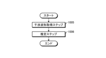
実施形態1に係る板状物の加工方法は、前述した板状物1を加工する方法である。板状の加工方法は、レーザー加工装置10の制御ユニット100の加工制御部101が、オペレータが入力ユニット120などを操作するなどして入力した加工条件を登録し、板状物1の表面3側が保持テーブル11の保持面12に載置され、制御ユニット100の加工制御部101がオペレータからの加工開始指示を受け付けると開始する。なお、加工条件は、加工対象の板状物1の材質及び厚み等を含む。板状物の加工方法は、図9に示すように、抵抗率検出ステップ1001と、判断ステップ1002と、加工条件選定ステップ1003と、レーザービーム照射ステップ1004とを実施する。 The method for processing a plate-like object according to the first embodiment is a method for processing the above-mentioned plate-like object 1. In the plate-shaped processing method, the processing control section 101 of the control unit 100 of the laser processing apparatus 10 registers the processing conditions inputted by the operator by operating the input unit 120, etc., and the surface 3 side of the plate-shaped object 1 is It is placed on the holding surface 12 of the holding table 11, and starts when the processing control section 101 of the control unit 100 receives a processing start instruction from the operator. Note that the processing conditions include the material, thickness, etc. of the plate-like object 1 to be processed. As shown in FIG. 9, the method for processing a plate-like object includes a resistivity detection step 1001, a determination step 1002, a processing condition selection step 1003, and a laser beam irradiation step 1004.

(抵抗率検出ステップ)
抵抗率検出ステップ1001は、実施形態1に係る抵抗率の測定方法を用いて保持テーブル11の保持面12に表面3側が載置された加工対象の板状物1の抵抗率71(図7に示す)を検出するステップである。抵抗率検出ステップ1001即ち実施形態1に係る抵抗率の測定方法は、保持テーブル11の保持面12に表面3側が載置された板状物1の抵抗率を検出する方法でもある。抵抗率検出ステップ1001即ち実施形態1に係る抵抗率の測定方法は、図10に示すように、干渉波形取得ステップ1005と、推定ステップ1006とを含む。
(Resistivity detection step)
In the resistivity detection step 1001, the resistivity 71 (as shown in FIG. This is the step of detecting (shown). The resistivity detection step 1001, that is, the resistivity measuring method according to the first embodiment, is also a method for detecting the resistivity of the plate-shaped object 1 whose front surface 3 side is placed on the holding surface 12 of the holding table 11. The resistivity detection step 1001, that is, the resistivity measurement method according to the first embodiment, includes an interference waveform acquisition step 1005 and an estimation step 1006, as shown in FIG.

(干渉波形取得ステップ)
干渉波形取得ステップ1005は、板状物1の裏面7に対して光源51からの光52を照射し、裏面7で反射した光521と、裏面7を透過し表面3で反射した光522との干渉波形60を取得するステップである。干渉波形取得ステップ1005では、レーザー加工装置10は、制御ユニット100の加工制御部101が保持テーブル11の保持面12に板状物1の表面3を吸引保持し、移動ユニット30を制御して保持テーブル11を加工領域に向けて移動するとともに、板状物1を分光干渉計50の下方に位置付ける。
(Interference waveform acquisition step)
In the interference waveform acquisition step 1005, the back surface 7 of the plate-shaped object 1 is irradiated with light 52 from the light source 51, and the light 521 reflected by the back surface 7 and the light 522 transmitted through the back surface 7 and reflected by the front surface 3 are combined. This is a step of acquiring an interference waveform 60. In the interference waveform acquisition step 1005, in the laser processing apparatus 10, the processing control section 101 of the control unit 100 suction-holds the surface 3 of the plate-shaped object 1 on the holding surface 12 of the holding table 11, and controls the moving unit 30 to hold it. The table 11 is moved toward the processing area, and the plate-shaped object 1 is positioned below the spectroscopic interferometer 50.

干渉波形取得ステップ1005では、レーザー加工装置10は、制御ユニット100の加工制御部101が分光干渉計50を制御して光源51から光52を出射して板状物1に照射するとともに、裏面7で反射した光521と表面3で反射した光522との干渉光を回折格子54で分光してラインセンサ55で受光する。干渉波形取得ステップ1005では、レーザー加工装置10は、分光干渉計50がラインセンサ55で光521と光522との干渉光を受光して、干渉波形60を取得し、取得した干渉波形60を制御ユニット100に出力する。 In the interference waveform acquisition step 1005 , in the laser processing apparatus 10 , the processing control section 101 of the control unit 100 controls the spectral interferometer 50 to emit light 52 from the light source 51 to irradiate the plate-like object 1 , and the back surface 7 The interference light of the light 521 reflected by the surface 3 and the light 522 reflected by the surface 3 is separated by the diffraction grating 54 and received by the line sensor 55. In the interference waveform acquisition step 1005, the laser processing device 10 causes the spectroscopic interferometer 50 to receive interference light between the light 521 and the light 522 with the line sensor 55, acquire an interference waveform 60, and control the acquired interference waveform 60. Output to unit 100.

(推定ステップ)
推定ステップ1006は、干渉波形取得ステップ1005で取得した干渉波形60に基づいて加工対象の板状物1の抵抗率71を推定するステップである。推定ステップ1006では、レーザー加工装置10は、制御ユニット100の加工制御部101が、干渉波形60から最大値61を抽出し、加工条件で定められた材質及び厚みの板状物1の抵抗率情報70を記憶部102から読み出す。推定ステップ1006では、レーザー加工装置10は、制御ユニット100の加工制御部101が、例えば、記憶部102から読み出した抵抗率情報70において干渉波形60から抽出した最大値61に対応した抵抗率71を抽出する。こうして、推定ステップ1006では、制御ユニット100の加工制御部101が、干渉波形取得ステップ1005において取得した干渉波形60の最大値61に基づいて加工対象の板状物1の抵抗率71を推定するとともに、推定の際には、記憶部102に記憶された抵抗率情報70に基づいて加工対象の板状物1の抵抗率71を逆算する。
(Estimation step)
The estimation step 1006 is a step of estimating the resistivity 71 of the plate-shaped object 1 to be processed based on the interference waveform 60 obtained in the interference waveform obtaining step 1005. In the estimation step 1006, in the laser processing apparatus 10, the processing control section 101 of the control unit 100 extracts the maximum value 61 from the interference waveform 60, and obtains resistivity information of the plate-like object 1 of the material and thickness determined by the processing conditions. 70 is read from the storage unit 102. In the estimation step 1006, the laser processing apparatus 10 calculates, for example, the resistivity 71 corresponding to the maximum value 61 extracted from the interference waveform 60 in the resistivity information 70 read from the storage section 102 by the processing control section 101 of the control unit 100. Extract. In this manner, in the estimation step 1006, the processing control section 101 of the control unit 100 estimates the resistivity 71 of the plate-shaped object 1 to be processed based on the maximum value 61 of the interference waveform 60 obtained in the interference waveform obtaining step 1005. , at the time of estimation, the resistivity 71 of the plate-shaped object 1 to be processed is calculated backward based on the resistivity information 70 stored in the storage unit 102.

(判断ステップ)
判断ステップ1002は、抵抗率検出ステップ1001を実施した後、検出した抵抗率71を有する加工対象の板状物1に対してレーザービーム21の照射による加工が可能か否かを判断するステップである。実施形態1において、判断ステップ1002では、制御ユニット100の加工制御部101が、記憶部102から判断条件80を読み出し、推定ステップ1006で推定した抵抗率71即ち抵抗率検出ステップ1001で検出した抵抗率71が第1の値未満であるか否かを判断して、加工が可能な否かを判断する。
(Judgment step)
Judgment step 1002 is a step of determining whether or not it is possible to process the plate-shaped object 1 to be processed having the detected resistivity 71 by irradiating the laser beam 21 after performing the resistivity detection step 1001. . In the first embodiment, in the judgment step 1002, the processing control section 101 of the control unit 100 reads out the judgment condition 80 from the storage section 102, and calculates the resistivity 71 estimated in the estimation step 1006, that is, the resistivity detected in the resistivity detection step 1001. 71 is less than the first value, and it is determined whether processing is possible.

実施形態1において、判断ステップ1002では、制御ユニット100の加工制御部101が、推定ステップ1006で推定した抵抗率71即ち抵抗率検出ステップ1001で検出した抵抗率71が第1の値未満であると判断すると、加工対象の板状物1に対してレーザービーム21の照射による加工が可能ではない(判断ステップ1002:No)と判断する。実施形態1において、判断ステップ1002では、制御ユニット100の加工制御部101が、加工対象の板状物1に対してレーザービーム21の照射による加工が可能ではないと判断すると、報知ユニットに報知させ(ステップ1010)、板状物の加工方法を終了する。 In the first embodiment, in the judgment step 1002, the processing control section 101 of the control unit 100 determines that the resistivity 71 estimated in the estimation step 1006, that is, the resistivity 71 detected in the resistivity detection step 1001 is less than the first value. If so, it is determined that the plate-like object 1 to be processed cannot be processed by irradiating the laser beam 21 (determination step 1002: No). In the first embodiment, in the determination step 1002, when the processing control section 101 of the control unit 100 determines that the plate-shaped object 1 to be processed cannot be processed by irradiation with the laser beam 21, it causes the notification unit to notify. (Step 1010), the method for processing a plate-shaped object is ended.

また、実施形態1において、判断ステップ1002では、制御ユニット100の加工制御部101が、推定ステップ1006で推定した抵抗率71即ち抵抗率検出ステップ1001で検出した抵抗率71が第1の値未満ではないと判断すると、加工対象の板状物1に対してレーザービーム21の照射による加工が可能である(判断ステップ1002:Yes)と判断する。実施形態1において、判断ステップ1002では、制御ユニット100の加工制御部101が、加工対象の板状物1に対してレーザービーム21の照射による加工が可能であると判断すると、加工条件選定ステップ1003に進む。 Further, in the first embodiment, in the judgment step 1002, the processing control section 101 of the control unit 100 determines that if the resistivity 71 estimated in the estimation step 1006, that is, the resistivity 71 detected in the resistivity detection step 1001 is less than the first value. If it is determined that there is not, it is determined that the plate-shaped object 1 to be processed can be processed by irradiating the laser beam 21 (determination step 1002: Yes). In the first embodiment, in the judgment step 1002, when the processing control section 101 of the control unit 100 judges that the plate-shaped object 1 to be processed can be processed by irradiation with the laser beam 21, the processing condition selection step 1003 is performed. Proceed to.

(加工条件選定ステップ)
加工条件選定ステップ1003は、推定ステップ1006で推定した抵抗率に対応する加工条件を選定するステップである。加工条件選定ステップ1003では、制御ユニット100の加工制御部101が、推定ステップ1006で推定した抵抗率71即ち抵抗率検出ステップ1001で検出した抵抗率71が第1の値以上でかつ第2の値未満であるか、又は第2の値以上でかつ第3の値未満であるかを判断する。
(Processing condition selection step)
Processing condition selection step 1003 is a step of selecting processing conditions corresponding to the resistivity estimated in estimation step 1006. In the processing condition selection step 1003, the processing control section 101 of the control unit 100 determines whether the resistivity 71 estimated in the estimation step 1006, that is, the resistivity 71 detected in the resistivity detection step 1001 is greater than or equal to the first value and is equal to or smaller than the second value. It is determined whether the value is less than a second value or greater than or equal to a second value and less than a third value.

加工条件選定ステップ1003では、制御ユニット100の加工制御部101が、推定ステップ1006で推定した抵抗率71即ち抵抗率検出ステップ1001で検出した抵抗率71が第1の値以上でかつ第2の値未満であると判断すると、判断条件80を参照して、オペレータが設定した加工条件81を選定する。また、加工条件選定ステップ1003では、制御ユニット100の加工制御部101が、推定ステップ1006で推定した抵抗率71即ち抵抗率検出ステップ1001で検出した抵抗率71が第2の値以上でかつ第3の値未満であると判断すると、判断条件80を参照して、加工条件82を選定する。 In the processing condition selection step 1003, the processing control section 101 of the control unit 100 determines whether the resistivity 71 estimated in the estimation step 1006, that is, the resistivity 71 detected in the resistivity detection step 1001 is greater than or equal to the first value and is equal to or smaller than the second value. If it is determined that the condition is less than 1, the processing condition 81 set by the operator is selected with reference to the judgment condition 80. In addition, in the processing condition selection step 1003, the processing control section 101 of the control unit 100 determines that the resistivity 71 estimated in the estimation step 1006, that is, the resistivity 71 detected in the resistivity detection step 1001 is equal to or higher than the second value, and If it is determined that it is less than the value, processing conditions 82 are selected with reference to determination conditions 80.

(レーザービーム照射ステップ)
レーザービーム照射ステップ1004は、加工条件選定ステップ1003で選定された加工条件81,82で加工対象の板状物1に対してレーザービーム21を照射して加工を施すステップである。レーザービーム照射ステップ1004では、レーザー加工装置10は、制御ユニット100の加工制御部101が、移動ユニット30を制御して、加工対象の板状物1を撮像ユニット40の下方に位置付け、撮像ユニット40で板状物1の裏面7を撮像させる。
(Laser beam irradiation step)
The laser beam irradiation step 1004 is a step in which the plate-shaped object 1 to be processed is irradiated with the laser beam 21 to perform processing under the processing conditions 81 and 82 selected in the processing condition selection step 1003. In the laser beam irradiation step 1004 , in the laser processing apparatus 10 , the processing control section 101 of the control unit 100 controls the moving unit 30 to position the plate-shaped object 1 to be processed below the imaging unit 40 . The back surface 7 of the plate-like object 1 is imaged.

レーザービーム照射ステップ1004では、レーザー加工装置10は、制御ユニット100の加工制御部101が撮像ユニット40が撮像して取得した画像から分割予定ライン4を検出し、分割予定ライン4とレーザービーム照射ユニット20との位置合わせを行うアライメントを遂行する。レーザービーム照射ステップ1004では、レーザー加工装置10は、制御ユニット100の加工制御部101が、加工条件選定ステップ1003で選定された加工条件81,82等に基づいて、図4に示すように、板状物1に対して透過性を有する波長のレーザービーム21の集光点22を基板2の内部に位置付けて、保持テーブル11とレーザービーム照射ユニット20とを分割予定ライン4に沿って相対的に移動させながら板状物1の裏面7側から板状物1に分割予定ライン4に沿ってパルス状のレーザービーム21を照射する。 In the laser beam irradiation step 1004, in the laser processing apparatus 10, the processing control section 101 of the control unit 100 detects the planned dividing line 4 from the image captured and acquired by the imaging unit 40, and the planned dividing line 4 and the laser beam irradiation unit 20. Alignment is performed to align with 20. In the laser beam irradiation step 1004, the laser processing apparatus 10 controls the processing control section 101 of the control unit 100 to control the processing conditions 81, 82, etc. selected in the processing condition selection step 1003, as shown in FIG. The condensing point 22 of the laser beam 21 having a wavelength that is transparent to the object 1 is positioned inside the substrate 2, and the holding table 11 and the laser beam irradiation unit 20 are relatively aligned along the planned dividing line 4. A pulsed laser beam 21 is irradiated onto the plate-like object 1 from the back surface 7 side of the plate-like object 1 along the dividing line 4 while moving the object.

すると、板状物1は、図4に示すように、レーザービーム21の波長が板状物1に対して透過性を有する波長を有するために、分割予定ライン4に沿って基板2の内部に改質層8が形成される。レーザービーム照射ステップ1004では、レーザー加工装置10は、全ての分割予定ライン4に沿って基板2の内部に改質層8を形成すると、レーザービーム照射ユニット20からのレーザービーム21の照射を停止し、保持テーブル11を搬入出領域まで移動させた後、保持面12の吸引保持を停止して、板状物の加工方法即ち加工動作を終了する。 Then, as shown in FIG. 4, the plate-like object 1 is inserted into the substrate 2 along the dividing line 4 because the wavelength of the laser beam 21 is transparent to the plate-like object 1. A modified layer 8 is formed. In the laser beam irradiation step 1004, the laser processing apparatus 10 stops irradiating the laser beam 21 from the laser beam irradiation unit 20 after forming the modified layer 8 inside the substrate 2 along all the planned dividing lines 4. After the holding table 11 is moved to the loading/unloading area, suction and holding of the holding surface 12 is stopped, and the method for processing a plate-shaped object, that is, the processing operation is completed.

以上説明した実施形態1に係る抵抗率の検出方法及び板状物の加工方法は、レーザー加工装置10の記憶部102に板状物1の抵抗率と干渉波形60の最大値61とを紐付けた抵抗率情報70を予め記憶しておき、加工対象の板状物1の干渉波形60を取得し、取得した干渉波形60の最大値61と抵抗率情報70とに基づいて加工対象の板状物1の抵抗率71を推定する。その結果、実施形態1に係る抵抗率の検出方法及び板状物の加工方法は、板状物1を加工することなく板状物1の加工性に対応した抵抗率71を判断することが可能になるという効果を奏する。 The method for detecting resistivity and the method for processing a plate-like object according to Embodiment 1 described above associates the resistivity of the plate-like object 1 and the maximum value 61 of the interference waveform 60 in the storage unit 102 of the laser processing device 10. The resistivity information 70 is stored in advance, the interference waveform 60 of the plate-like object 1 to be processed is acquired, and the plate-like object to be processed is determined based on the maximum value 61 of the obtained interference waveform 60 and the resistivity information 70. Estimate the resistivity 71 of object 1. As a result, the method for detecting resistivity and the method for processing a plate-like object according to the first embodiment can determine the resistivity 71 corresponding to the workability of the plate-like object 1 without processing the plate-like object 1. It has the effect of becoming

〔変形例〕
本発明の実施形態1の変形例に係る抵抗率の検出方法及び板状物の加工方法を図面に基づいて説明する。図11は、実施形態1の変形例に係る抵抗率の検出方法及び板状物の加工方法を実施するレーザー加工装置の制御ユニットの記憶部が記憶した抵抗率情報を示す図である。図12は、実施形態1の変形例に係る抵抗率の検出方法及び板状物の加工方法を実施するレーザー加工装置の分光干渉計が取得した干渉波形をフーリエ変換して得られる波形の一例を示す図である。
[Modified example]
A method for detecting resistivity and a method for processing a plate-like object according to a modification of Embodiment 1 of the present invention will be explained based on the drawings. FIG. 11 is a diagram showing resistivity information stored in a storage unit of a control unit of a laser processing apparatus that implements a resistivity detection method and a plate-like object processing method according to a modification of the first embodiment. FIG. 12 shows an example of a waveform obtained by Fourier transforming an interference waveform obtained by a spectral interferometer of a laser processing device that implements a method for detecting resistivity and a method for processing a plate-shaped object according to a modification of Embodiment 1. FIG.

実施形態1の変形例に係る抵抗率の検出方法及び板状物の加工方法は、レーザー加工装置10の制御ユニット100が抵抗率情報70の代わりに図11に示す抵抗率情報70-1を予め記憶部102に記憶し、推定ステップ1006において、干渉波形取得ステップ1005で取得した干渉波形60をフーリエ変換して得られる図12に示す波形60-1の最大値61-1と、抵抗率情報70-1とに基づいて、板状物1の抵抗率71を推定する事以外、実施形態1と同じである。 In the method for detecting resistivity and the method for processing a plate-like object according to the modification of the first embodiment, the control unit 100 of the laser processing apparatus 10 uses resistivity information 70-1 shown in FIG. 11 in advance, instead of the resistivity information 70. The maximum value 61-1 of the waveform 60-1 shown in FIG. This is the same as the first embodiment except that the resistivity 71 of the plate-like object 1 is estimated based on -1.

抵抗率情報70-1は、同一の材質でかつ同一の厚みの複数の板状物1の抵抗率と、抵抗率に対応する干渉波形60をフーリエ変換して得られる図12に例示する波形60-1の最大値61-1とを紐付けて、これらの関係を示すものである。即ち、抵抗率情報70は、同一の材質でかつ同一の厚みの複数の板状物1の抵抗率と、抵抗率に対応する干渉波形60をフーリエ変換して得られる波形60-1の最大値61-1とを一対一で対応付けたものである。なお、図11に示された抵抗率情報70-1は、横軸が同一の材質でかつ厚みの複数の板状物1の抵抗率を示し、縦軸が干渉波形60をフーリエ変換した波形60-1の最大値61-1を示している。また、図12に示された波形60-1は、横軸が板状物1の裏面7の高さを示し、縦軸が信号強度を示している。 The resistivity information 70-1 is a waveform 60 illustrated in FIG. 12 obtained by Fourier transforming the resistivities of a plurality of plate-like objects 1 made of the same material and having the same thickness and the interference waveform 60 corresponding to the resistivity. This relationship is shown by linking the maximum value of -1 with 61-1. That is, the resistivity information 70 is the maximum value of the waveform 60-1 obtained by Fourier transforming the resistivity of a plurality of plate-like objects 1 made of the same material and the same thickness and the interference waveform 60 corresponding to the resistivity. 61-1 in one-to-one correspondence. In the resistivity information 70-1 shown in FIG. 11, the horizontal axis indicates the resistivity of a plurality of plate-like objects 1 made of the same material and the same thickness, and the vertical axis indicates the waveform 60 obtained by Fourier transforming the interference waveform 60. The maximum value of -1 is 61-1. Further, in the waveform 60-1 shown in FIG. 12, the horizontal axis indicates the height of the back surface 7 of the plate-shaped object 1, and the vertical axis indicates the signal intensity.

抵抗率情報70-1は、抵抗率が既知の同一の材質でかつ同一の厚みの複数の板状物1に分光干渉計50が光52を照射して干渉波形60を取得し、既知の抵抗率と干渉波形60をフーリエ変換した波形60-1の最大値61-1の実測値72-1とを最小二乗法により近似して求められている。記憶部102は、実施形態1と同様に、板状物1の材質及び厚み毎に対応した抵抗率情報70-1を記憶している。このように、抵抗率情報70-1は、種々の抵抗率の板状物1から取得した干渉波形60をフーリエ変換し、各々の板状物1の抵抗率と、抵抗率に対応する干渉波形60をフーリエ変換した波形60-1の最大値61-1とを紐付けたものである。 The resistivity information 70-1 is obtained by the spectral interferometer 50 irradiating the light 52 onto a plurality of plate-like objects 1 made of the same material with known resistivity and the same thickness to obtain an interference waveform 60. It is obtained by approximating the actual value 72-1 of the maximum value 61-1 of the waveform 60-1 obtained by Fourier transforming the interference waveform 60 using the least squares method. The storage unit 102 stores resistivity information 70-1 corresponding to each material and thickness of the plate-like object 1, as in the first embodiment. In this way, the resistivity information 70-1 is obtained by Fourier transforming the interference waveforms 60 obtained from the plate-like objects 1 with various resistivities, and obtains the resistivity of each plate-like object 1 and the interference waveform corresponding to the resistivity. The maximum value 61-1 of the waveform 60-1 obtained by Fourier transforming 60 is linked.

実施形態1の変形例に係る抵抗率の検出方法及び板状物の加工方法において、推定ステップ1006では、レーザー加工装置10は、制御ユニット100の加工制御部101が、干渉波形取得ステップ1005で加工対象の板状物1から取得した干渉波形60をフーリエ変換する。実施形態1の変形例において、推定ステップ1006では、レーザー加工装置10は、制御ユニット100の加工制御部101が、フーリエ変換後の波形60-1から最大値61-1を抽出し、加工条件で定められた材質及び厚みの板状物1の抵抗率情報70-1を記憶部102から読み出す。 In the method for detecting resistivity and the method for processing a plate-shaped object according to the modification of the first embodiment, in the estimation step 1006, the processing control section 101 of the control unit 100 performs processing in the laser processing apparatus 10 in the interference waveform acquisition step 1005. The interference waveform 60 obtained from the target plate-like object 1 is subjected to Fourier transformation. In the modification of the first embodiment, in the estimation step 1006, the processing control section 101 of the control unit 100 extracts the maximum value 61-1 from the Fourier-transformed waveform 60-1, and extracts the maximum value 61-1 under the processing conditions. Resistivity information 70-1 of the plate-like object 1 of the determined material and thickness is read out from the storage unit 102.

実施形態1の変形例において、推定ステップ1006では、レーザー加工装置10は、制御ユニット100の加工制御部101が、記憶部102から読み出した抵抗率情報70-1において波形60-1から抽出した最大値61-1に対応した抵抗率71を抽出する。こうして、推定ステップ1006では、制御ユニット100の加工制御部101が、干渉波形取得ステップ1005において取得した干渉波形60をフーリエ変換し、変換後の波形60-1に基づいて加工対象の板状物1の抵抗率71を推定するとともに、推定の際には、記憶部102に記憶された抵抗率情報70-1に基づいて加工対象の板状物1の抵抗率71を逆算する。 In the modification of the first embodiment, in the estimation step 1006, the laser processing apparatus 10 calculates the maximum Resistivity 71 corresponding to value 61-1 is extracted. Thus, in the estimation step 1006, the processing control section 101 of the control unit 100 performs Fourier transform on the interference waveform 60 obtained in the interference waveform obtaining step 1005, and based on the transformed waveform 60-1, the processing control section 101 of the control unit 100 At the same time as estimating the resistivity 71 of the plate-shaped object 1 to be processed, the resistivity 71 of the plate-shaped object 1 to be processed is calculated based on the resistivity information 70-1 stored in the storage unit 102.

実施形態1の変形例に係る抵抗率の検出方法及び板状物の加工方法は、レーザー加工装置10の記憶部102に板状物1の抵抗率と干渉波形60をフーリエ変換した波形60-1の最大値61-1とを紐付けた抵抗率情報70-1を予め記憶しておき、加工対象の板状物1の干渉波形60を取得し、取得した干渉波形60のフーリエ変換後の波形60-1の最大値61-1と抵抗率情報70-1とに基づいて加工対象の板状物1の抵抗率71を推定するので、実施形態1と同様に、板状物1を加工することなく板状物1の加工性に対応した抵抗率71を判断することが可能になるという効果を奏する。 The method of detecting resistivity and the method of processing a plate-like object according to a modification of the first embodiment includes a waveform 60-1 obtained by Fourier-transforming the resistivity of the plate-like object 1 and the interference waveform 60 in the storage unit 102 of the laser processing device 10. The resistivity information 70-1 linked to the maximum value 61-1 of Since the resistivity 71 of the plate-like object 1 to be processed is estimated based on the maximum value 61-1 of 60-1 and the resistivity information 70-1, the plate-like object 1 is processed in the same manner as in the first embodiment. This has the effect that it becomes possible to determine the resistivity 71 corresponding to the workability of the plate-like object 1 without any problems.

〔実施形態2〕
本発明の実施形態2に係る抵抗率の検出方法及び板状物の加工方法を図面に基づいて説明する。図13は、実施形態2に係る抵抗率の検出方法及び板状物の加工方法を実施するレーザー加工装置の構成例を示す斜視図である。図14は、実施形態2に係る抵抗率の測定方法の流れを示すフローチャートである。なお、図13及び図14は、実施形態1と同一部分に同一符号を付して説明を省略する。
[Embodiment 2]
A method for detecting resistivity and a method for processing a plate-like object according to Embodiment 2 of the present invention will be explained based on the drawings. FIG. 13 is a perspective view showing a configuration example of a laser processing apparatus that implements the resistivity detection method and the plate-shaped object processing method according to the second embodiment. FIG. 14 is a flowchart showing the flow of the resistivity measuring method according to the second embodiment. In addition, in FIGS. 13 and 14, the same parts as in Embodiment 1 are denoted by the same reference numerals, and the description thereof will be omitted.

実施形態2に係る抵抗率の検出方法及び板状物の加工方法は、レーザー加工装置10の制御ユニット100が情報取得部103を備え、板状物の加工方法の抵抗率検出ステップ1001即ち抵抗率の検出方法が異なること以外、実施形態1及び実施形態1の変形例と同一である。制御ユニット100の情報取得部103は、抵抗率情報70,70-1を取得し、記憶部102に記憶するものである。情報取得部103の機能は、演算処理装置が記憶装置に記憶されているコンピュータプログラムに従って演算処理を実施することにより実現される。 In the method for detecting resistivity and the method for processing a plate-like object according to the second embodiment, the control unit 100 of the laser processing apparatus 10 includes an information acquisition section 103, and the resistivity detection step 1001 of the method for processing the plate-like object, that is, the resistivity This embodiment is the same as the first embodiment and the modification of the first embodiment except that the detection method is different. The information acquisition section 103 of the control unit 100 acquires the resistivity information 70, 70-1 and stores it in the storage section 102. The functions of the information acquisition unit 103 are realized by the arithmetic processing unit performing arithmetic processing according to a computer program stored in a storage device.

実施形態2に係る抵抗率の検出方法及び板状物の加工方法は、抵抗率検出ステップ1001即ち抵抗率の検出方法が、図14に示すように、記憶ステップ1007を更に備える。記憶ステップ1007は、実施形態1の抵抗率検出ステップ1001を種々の抵抗率を有する板状物1に対して行い、抵抗率情報70,70-1を予め記憶部102に記憶するステップである。記憶ステップ1007では、レーザー加工装置10は、制御ユニット100の情報取得部103が、加工対象の板状物1と同一の材質であり同一の厚みでかつ抵抗率が既知である複数の板状物1を保持テーブル11の保持面12に順に保持し、分光干渉計50で各板状物1の干渉波形60を取得する。 In the resistivity detection method and plate-like object processing method according to the second embodiment, the resistivity detection step 1001, that is, the resistivity detection method, further includes a storage step 1007, as shown in FIG. The storage step 1007 is a step in which the resistivity detection step 1001 of the first embodiment is performed on the plate-like objects 1 having various resistivities, and the resistivity information 70, 70-1 is stored in the storage unit 102 in advance. In the storage step 1007, the information acquisition unit 103 of the control unit 100 of the laser processing apparatus 10 stores a plurality of plate-like objects that are made of the same material, have the same thickness, and have a known resistivity as the plate-like object 1 to be processed. 1 are sequentially held on the holding surface 12 of the holding table 11, and the interference waveform 60 of each plate-like object 1 is acquired by the spectroscopic interferometer 50.

実施形態2において、推定ステップ1006において、レーザー加工装置10は、制御ユニット100の加工制御部101が実施形態1及び変形例と同様に、記憶ステップ1007で記憶された抵抗率情報70,70-1に基づいて加工対象の板状物1の抵抗率71を逆算する。また、実施形態2において、推定ステップ1006において、レーザー加工装置10は、制御ユニット100の加工制御部101が実施形態1の変形例と同様に、干渉波形取得ステップ1005で取得した干渉波形60をフーリエ変換し、フーリエ変換後の波形60-1の最大値61-1に基づいて板状物の抵抗率を推定する。 In the second embodiment, in the estimation step 1006, the processing control section 101 of the control unit 100 in the laser processing apparatus 10 uses the resistivity information 70, 70-1 stored in the storage step 1007, as in the first embodiment and the modified example. The resistivity 71 of the plate-like object 1 to be processed is calculated backward based on . In addition, in the second embodiment, in the estimation step 1006, the laser processing apparatus 10 uses the Fourier The resistivity of the plate-shaped object is estimated based on the maximum value 61-1 of the waveform 60-1 after Fourier transformation.

実施形態2に係る抵抗率の検出方法及び板状物の加工方法は、抵抗率情報70,70-1を記憶ステップ1007で記憶し、加工対象の板状物1の干渉波形60を取得し、取得した干渉波形60の最大値61又はフーリエ変換後の波形60-1の最大値61-1と抵抗率情報70-1とに基づいて加工対象の板状物1の抵抗率71を推定するので、実施形態1と同様に、板状物1を加工することなく板状物1の加工性に対応した抵抗率71を判断することが可能になるという効果を奏する。 The method for detecting resistivity and the method for processing a plate-like object according to the second embodiment stores the resistivity information 70, 70-1 in a storage step 1007, acquires the interference waveform 60 of the plate-like object 1 to be processed, The resistivity 71 of the plate-shaped object 1 to be processed is estimated based on the maximum value 61 of the acquired interference waveform 60 or the maximum value 61-1 of the waveform 60-1 after Fourier transformation and the resistivity information 70-1. , as in the first embodiment, it is possible to determine the resistivity 71 corresponding to the workability of the plate-like object 1 without processing the plate-like object 1.

なお、本発明は、上記実施形態に限定されるものではない。即ち、本発明の骨子を逸脱しない範囲で種々変形して実施することができる。例えば、本発明では、抵抗率の測定方法即ち干渉波形取得ステップ1005及び推定ステップ1006のみ、又は、記憶ステップ1007、干渉波形取得ステップ1005及び推定ステップ1006のみを実施し、判断ステップ1002、加工条件選定ステップ1003及びレーザービーム照射ステップ1004を必ずしも実施しなくてもよい。また、本発明では、同一の材質であり同一の厚みでかつ抵抗率が既知である複数の板状物1に関する抵抗率情報70,70-1を、異なる厚み毎に取得して、取得した複数の厚みそれぞれの抵抗率情報70,70-1をレーザー加工装置10の記憶部102に記憶しておいても良い。この場合、様々な厚みの板状物1の抵抗率71を推定することが可能となる。 Note that the present invention is not limited to the above embodiments. That is, various modifications can be made without departing from the gist of the invention. For example, in the present invention, only the resistivity measurement method, that is, the interference waveform acquisition step 1005 and the estimation step 1006, or the storage step 1007, the interference waveform acquisition step 1005, and the estimation step 1006 are performed, and the judgment step 1002 and the processing condition selection are performed. Step 1003 and laser beam irradiation step 1004 do not necessarily have to be performed. Further, in the present invention, resistivity information 70, 70-1 regarding a plurality of plate-like objects 1 made of the same material, the same thickness, and having known resistivity is acquired for each different thickness, and The resistivity information 70, 70-1 for each thickness may be stored in the storage unit 102 of the laser processing apparatus 10. In this case, it becomes possible to estimate the resistivity 71 of the plate-like object 1 having various thicknesses.

1 板状物
3 表面(第二の面)
7 裏面(第一の面)
21 レーザービーム
51 光源
52 光
60 干渉波形
60-1 波形
61,61-1 最大値
70,70-1 抵抗率情報
71 抵抗率
81,82 加工条件
521 光(第一の面で反射した光)
522 光(第二の面で反射した光)
1001 抵抗率検出ステップ
1002 判断ステップ
1003 加工条件選定ステップ
1004 レーザービーム照射ステップ
1005 干渉波形取得ステップ
1006 推定ステップ
1007 記憶ステップ
1 Plate-shaped object 3 Surface (second surface)
7 Back side (first side)
21 Laser beam 51 Light source 52 Light 60 Interference waveform 60-1 Waveform 61, 61-1 Maximum value 70, 70-1 Resistivity information 71 Resistivity 81, 82 Processing conditions 521 Light (light reflected on the first surface)
522 Light (light reflected on the second surface)
1001 Resistivity detection step 1002 Judgment step 1003 Processing condition selection step 1004 Laser beam irradiation step 1005 Interference waveform acquisition step 1006 Estimation step 1007 Storage step

Claims (7)

第一の面と、該第一の面の反対側の第二の面とを有する板状物の抵抗率を検出する抵抗率の検出方法であって、
板状物の該第一の面に対して光源から光を照射し、該第一の面で反射した光と、該第一の面を透過し該第二の面で反射した光との干渉波形を取得する干渉波形取得ステップと、
該干渉波形取得ステップで取得した干渉波形に基づいて該板状物の抵抗率を推定する推定ステップと、
を含むことを特徴とする、抵抗率の検出方法。
A resistivity detection method for detecting the resistivity of a plate-like object having a first surface and a second surface opposite to the first surface, the method comprising:
Light is irradiated from a light source onto the first surface of a plate-shaped object, and interference occurs between the light reflected from the first surface and the light transmitted through the first surface and reflected from the second surface. an interference waveform acquisition step of acquiring a waveform;
an estimation step of estimating the resistivity of the plate-like object based on the interference waveform acquired in the interference waveform acquisition step;
A method for detecting resistivity, comprising:
該推定ステップでは、該干渉波形取得ステップで取得した干渉波形の最大値に基づいて該板状物の抵抗率を推定することを特徴とする、請求項1に記載の抵抗率の検出方法。 2. The resistivity detection method according to claim 1, wherein in the estimation step, the resistivity of the plate-like object is estimated based on the maximum value of the interference waveform acquired in the interference waveform acquisition step. 該干渉波形取得ステップを種々の抵抗率を有する板状物に対して行い、各々の板状物の抵抗率と、該抵抗率に対応する干渉波形の最大値と、を紐付けた抵抗率情報を予め記憶しておく記憶ステップを更に備え、
該推定ステップは、記憶ステップで記憶された該抵抗率情報に基づいて板状物の抵抗率を逆算することを特徴とする、請求項2に記載の抵抗率の検出方法。
The interference waveform acquisition step is performed on plate-like objects having various resistivities, and resistivity information is obtained that links the resistivity of each plate-like object and the maximum value of the interference waveform corresponding to the resistivity. further comprising a memorization step for memorizing in advance,
3. The resistivity detection method according to claim 2, wherein the estimating step includes back calculating the resistivity of the plate-like object based on the resistivity information stored in the storing step.
該推定ステップでは、該干渉波形取得ステップで取得した干渉波形をフーリエ変換し、変換後の波形の最大値に基づいて該板状物の抵抗率を推定することを特徴とする、請求項1に記載の抵抗率の検出方法。 According to claim 1, in the estimation step, the interference waveform acquired in the interference waveform acquisition step is Fourier transformed, and the resistivity of the plate-like object is estimated based on the maximum value of the transformed waveform. Method of detecting resistivity as described. 該干渉波形取得ステップを種々の抵抗率を有する板状物に対して行い各々の板状物の抵抗率と、該抵抗率に対応する干渉波形をフーリエ変換した波形の最大値と、を紐付けた抵抗率情報を予め記憶しておく記憶ステップを更に備え、
該推定ステップは、記憶ステップで記憶された該抵抗率情報に基づいて板状物の抵抗率を逆算することを特徴とする、請求項4に記載の抵抗率の検出方法。
The interference waveform acquisition step is performed on plate-like objects having various resistivities, and the resistivity of each plate-like object is linked to the maximum value of the waveform obtained by Fourier transforming the interference waveform corresponding to the resistivity. further comprising a storage step for storing resistivity information in advance,
5. The resistivity detection method according to claim 4, wherein the estimating step calculates the resistivity of the plate-like object based on the resistivity information stored in the storing step.
第一の面と、該第一の面の反対側の第二の面とを有する板状物を加工する板状物の加工方法であって、
請求項1乃至請求項5のうちのいずれか一項に記載の抵抗率の検出方法を用いて板状物の抵抗率を検出する抵抗率検出ステップと、
該抵抗率に対応する加工条件を選定する加工条件選定ステップと、
該加工条件選定ステップで選定された加工条件で該板状物に対してレーザービームを照射して加工を施すレーザービーム照射ステップと、
を実施することを特徴とする、板状物の加工方法。
A method for processing a plate-like object having a first surface and a second surface opposite to the first surface, the method comprising:
A resistivity detection step of detecting the resistivity of the plate-like object using the resistivity detection method according to any one of claims 1 to 5;
a processing condition selection step of selecting processing conditions corresponding to the resistivity;
a laser beam irradiation step of performing processing by irradiating the plate-like object with a laser beam under the processing conditions selected in the processing condition selection step;
A method for processing a plate-shaped object, characterized by carrying out the following.
該抵抗率検出ステップを実施した後、検出した抵抗率を有する板状物に対して該レーザービームの照射による加工が可能か否かを判断する判断ステップを更に含むことを特徴とする、請求項6に記載の板状物の加工方法。 Claim characterized in that, after performing the resistivity detection step, the method further includes a determination step of determining whether or not a plate-like object having the detected resistivity can be processed by irradiation with the laser beam. 6. The method for processing a plate-shaped object according to 6.
JP2022095217A 2022-06-13 2022-06-13 Resistivity detection method and plate-shaped object processing method Pending JP2023181853A (en)

Priority Applications (6)

Application Number Priority Date Filing Date Title
JP2022095217A JP2023181853A (en) 2022-06-13 2022-06-13 Resistivity detection method and plate-shaped object processing method
US18/327,146 US12508674B2 (en) 2022-06-13 2023-06-01 Detection method of resistivity and processing method of plate-shaped workpiece
DE102023205160.5A DE102023205160A1 (en) 2022-06-13 2023-06-02 RESISTANCE DETECTION METHOD AND MACHINING METHOD FOR A PLATE-SHAPED WORKPIECE
KR1020230072015A KR20230171387A (en) 2022-06-13 2023-06-05 Method of detecting resistivity and method of processing plate-shaped object
TW112121182A TW202349479A (en) 2022-06-13 2023-06-07 Detection method of resistivity and processing method of plate-shaped workpiece
CN202310682878.7A CN117233096A (en) 2022-06-13 2023-06-09 Method for detecting resistivity and method for processing plate-like object

Applications Claiming Priority (1)

Application Number Priority Date Filing Date Title
JP2022095217A JP2023181853A (en) 2022-06-13 2022-06-13 Resistivity detection method and plate-shaped object processing method

Publications (1)

Publication Number Publication Date
JP2023181853A true JP2023181853A (en) 2023-12-25

Family

ID=88874017

Family Applications (1)

Application Number Title Priority Date Filing Date
JP2022095217A Pending JP2023181853A (en) 2022-06-13 2022-06-13 Resistivity detection method and plate-shaped object processing method

Country Status (6)

Country Link
US (1) US12508674B2 (en)
JP (1) JP2023181853A (en)
KR (1) KR20230171387A (en)
CN (1) CN117233096A (en)
DE (1) DE102023205160A1 (en)
TW (1) TW202349479A (en)

Citations (2)

* Cited by examiner, † Cited by third party
Publication number Priority date Publication date Assignee Title
JP2021074794A (en) * 2019-11-05 2021-05-20 スピードファム株式会社 Polishing device
JP2022028362A (en) * 2020-08-03 2022-02-16 株式会社ディスコ Wafer, wafer manufacturing method, and device chip manufacturing method

Family Cites Families (10)

* Cited by examiner, † Cited by third party
Publication number Priority date Publication date Assignee Title
JP4505891B2 (en) * 1999-09-06 2010-07-21 Jsr株式会社 Chemical mechanical polishing aqueous dispersion used in the manufacture of semiconductor devices
US6407546B1 (en) * 2000-04-07 2002-06-18 Cuong Duy Le Non-contact technique for using an eddy current probe for measuring the thickness of metal layers disposed on semi-conductor wafer products
JP3408805B2 (en) 2000-09-13 2003-05-19 浜松ホトニクス株式会社 Cutting origin region forming method and workpiece cutting method
US7106425B1 (en) * 2000-09-20 2006-09-12 Kla-Tencor Technologies Corp. Methods and systems for determining a presence of defects and a thin film characteristic of a specimen
EP2232195B1 (en) * 2007-12-14 2015-03-18 Zygo Corporation Analyzing surface structure using scanning interferometry
JP4427594B2 (en) * 2008-08-11 2010-03-10 三菱重工業株式会社 Resistivity inspection method and apparatus
JP2012021916A (en) * 2010-07-15 2012-02-02 Disco Abrasive Syst Ltd Thickness detector and grinder
JP5985896B2 (en) * 2012-06-12 2016-09-06 株式会社ディスコ Wafer processing method and laser processing apparatus
US11642743B2 (en) * 2017-11-07 2023-05-09 Hamamatsu Photonics K.K. Laser processing method, and laser processing device
JP7481090B2 (en) * 2019-01-09 2024-05-10 株式会社ディスコ Thickness measuring device, and processing device equipped with thickness measuring device

Patent Citations (2)

* Cited by examiner, † Cited by third party
Publication number Priority date Publication date Assignee Title
JP2021074794A (en) * 2019-11-05 2021-05-20 スピードファム株式会社 Polishing device
JP2022028362A (en) * 2020-08-03 2022-02-16 株式会社ディスコ Wafer, wafer manufacturing method, and device chip manufacturing method

Also Published As

Publication number Publication date
US12508674B2 (en) 2025-12-30
KR20230171387A (en) 2023-12-20
CN117233096A (en) 2023-12-15
US20230398641A1 (en) 2023-12-14
DE102023205160A1 (en) 2023-12-14
TW202349479A (en) 2023-12-16

Similar Documents

Publication Publication Date Title
TWI610762B (en) Processing device
CN104552625B (en) Processing unit (plant)
TWI806095B (en) Laser processing device, wafer processing system and control method for laser processing device
CN102901445A (en) Device and method for detecting micro-electronic packaging process quality based on photo-thermal imaging
JP5957852B2 (en) Inspection apparatus and inspection method for semiconductor device
CN109382591B (en) Laser processing method
TWI888413B (en) Laser processing equipment
JP5484787B2 (en) Cross-sectional shape detection method, machining apparatus, and cross-sectional shape detection program
KR20170074169A (en) Inspection apparatus
TW202024563A (en) Thickness measuring apparatus
JP2015078852A (en) Alignment method
JP7285636B2 (en) Plate-like material processing method
JP2015072197A (en) Shape measuring apparatus, structure manufacturing system, shape measuring method, structure manufacturing method, and shape measuring program
US20080094087A1 (en) Device for detecting chip location and method of detecting chip location using the device
JP7692304B2 (en) Machining device and vibration detection method
JP2023181853A (en) Resistivity detection method and plate-shaped object processing method
KR102557511B1 (en) Inspection apparatus
JP7285637B2 (en) Plate-like material processing method
WO2016056109A1 (en) Analysis device and analysis method
TW202110562A (en) Method of confirming optical axis of laser processing apparatus
JP7450447B2 (en) laser processing equipment
JP7266430B2 (en) Laser processing equipment
JP2026017037A (en) Processing device, microscope, method for generating three-dimensional images, and method for processing workpieces
JP2024006434A (en) Inspection method for laser processing equipment and laser processing equipment
JP2003161604A (en) Height measuring method and height measuring device

Legal Events

Date Code Title Description
A621 Written request for application examination

Free format text: JAPANESE INTERMEDIATE CODE: A621

Effective date: 20250421

A131 Notification of reasons for refusal

Free format text: JAPANESE INTERMEDIATE CODE: A131

Effective date: 20260120

A977 Report on retrieval

Free format text: JAPANESE INTERMEDIATE CODE: A971007

Effective date: 20260122