JP2023000275A - Display device - Google Patents
Display device Download PDFInfo
- Publication number
- JP2023000275A JP2023000275A JP2021101007A JP2021101007A JP2023000275A JP 2023000275 A JP2023000275 A JP 2023000275A JP 2021101007 A JP2021101007 A JP 2021101007A JP 2021101007 A JP2021101007 A JP 2021101007A JP 2023000275 A JP2023000275 A JP 2023000275A
- Authority
- JP
- Japan
- Prior art keywords
- display
- liquid crystal
- bus lines
- bus line
- color
- Prior art date
- Legal status (The legal status is an assumption and is not a legal conclusion. Google has not performed a legal analysis and makes no representation as to the accuracy of the status listed.)
- Pending
Links
Images


Classifications
-
- G—PHYSICS
- G02—OPTICS
- G02F—OPTICAL DEVICES OR ARRANGEMENTS FOR THE CONTROL OF LIGHT BY MODIFICATION OF THE OPTICAL PROPERTIES OF THE MEDIA OF THE ELEMENTS INVOLVED THEREIN; NON-LINEAR OPTICS; FREQUENCY-CHANGING OF LIGHT; OPTICAL LOGIC ELEMENTS; OPTICAL ANALOGUE/DIGITAL CONVERTERS
- G02F1/00—Devices or arrangements for the control of the intensity, colour, phase, polarisation or direction of light arriving from an independent light source, e.g. switching, gating or modulating; Non-linear optics
- G02F1/01—Devices or arrangements for the control of the intensity, colour, phase, polarisation or direction of light arriving from an independent light source, e.g. switching, gating or modulating; Non-linear optics for the control of the intensity, phase, polarisation or colour
- G02F1/13—Devices or arrangements for the control of the intensity, colour, phase, polarisation or direction of light arriving from an independent light source, e.g. switching, gating or modulating; Non-linear optics for the control of the intensity, phase, polarisation or colour based on liquid crystals, e.g. single liquid crystal display cells
- G02F1/133—Constructional arrangements; Operation of liquid crystal cells; Circuit arrangements
- G02F1/1333—Constructional arrangements; Manufacturing methods
- G02F1/1347—Arrangement of liquid crystal layers or cells in which the final condition of one light beam is achieved by the addition of the effects of two or more layers or cells
- G02F1/13471—Arrangement of liquid crystal layers or cells in which the final condition of one light beam is achieved by the addition of the effects of two or more layers or cells in which all the liquid crystal cells or layers remain transparent, e.g. FLC, ECB, DAP, HAN, TN, STN, SBE-LC cells
-
- G—PHYSICS
- G02—OPTICS
- G02F—OPTICAL DEVICES OR ARRANGEMENTS FOR THE CONTROL OF LIGHT BY MODIFICATION OF THE OPTICAL PROPERTIES OF THE MEDIA OF THE ELEMENTS INVOLVED THEREIN; NON-LINEAR OPTICS; FREQUENCY-CHANGING OF LIGHT; OPTICAL LOGIC ELEMENTS; OPTICAL ANALOGUE/DIGITAL CONVERTERS
- G02F1/00—Devices or arrangements for the control of the intensity, colour, phase, polarisation or direction of light arriving from an independent light source, e.g. switching, gating or modulating; Non-linear optics
- G02F1/01—Devices or arrangements for the control of the intensity, colour, phase, polarisation or direction of light arriving from an independent light source, e.g. switching, gating or modulating; Non-linear optics for the control of the intensity, phase, polarisation or colour
- G02F1/13—Devices or arrangements for the control of the intensity, colour, phase, polarisation or direction of light arriving from an independent light source, e.g. switching, gating or modulating; Non-linear optics for the control of the intensity, phase, polarisation or colour based on liquid crystals, e.g. single liquid crystal display cells
- G02F1/133—Constructional arrangements; Operation of liquid crystal cells; Circuit arrangements
- G02F1/1333—Constructional arrangements; Manufacturing methods
-
- G—PHYSICS
- G02—OPTICS
- G02F—OPTICAL DEVICES OR ARRANGEMENTS FOR THE CONTROL OF LIGHT BY MODIFICATION OF THE OPTICAL PROPERTIES OF THE MEDIA OF THE ELEMENTS INVOLVED THEREIN; NON-LINEAR OPTICS; FREQUENCY-CHANGING OF LIGHT; OPTICAL LOGIC ELEMENTS; OPTICAL ANALOGUE/DIGITAL CONVERTERS
- G02F1/00—Devices or arrangements for the control of the intensity, colour, phase, polarisation or direction of light arriving from an independent light source, e.g. switching, gating or modulating; Non-linear optics
- G02F1/01—Devices or arrangements for the control of the intensity, colour, phase, polarisation or direction of light arriving from an independent light source, e.g. switching, gating or modulating; Non-linear optics for the control of the intensity, phase, polarisation or colour
- G02F1/13—Devices or arrangements for the control of the intensity, colour, phase, polarisation or direction of light arriving from an independent light source, e.g. switching, gating or modulating; Non-linear optics for the control of the intensity, phase, polarisation or colour based on liquid crystals, e.g. single liquid crystal display cells
- G02F1/133—Constructional arrangements; Operation of liquid crystal cells; Circuit arrangements
- G02F1/136—Liquid crystal cells structurally associated with a semi-conducting layer or substrate, e.g. cells forming part of an integrated circuit
- G02F1/1362—Active matrix addressed cells
- G02F1/136286—Wiring, e.g. gate line, drain line
- G02F1/13629—Multilayer wirings
-
- G—PHYSICS
- G02—OPTICS
- G02F—OPTICAL DEVICES OR ARRANGEMENTS FOR THE CONTROL OF LIGHT BY MODIFICATION OF THE OPTICAL PROPERTIES OF THE MEDIA OF THE ELEMENTS INVOLVED THEREIN; NON-LINEAR OPTICS; FREQUENCY-CHANGING OF LIGHT; OPTICAL LOGIC ELEMENTS; OPTICAL ANALOGUE/DIGITAL CONVERTERS
- G02F1/00—Devices or arrangements for the control of the intensity, colour, phase, polarisation or direction of light arriving from an independent light source, e.g. switching, gating or modulating; Non-linear optics
- G02F1/01—Devices or arrangements for the control of the intensity, colour, phase, polarisation or direction of light arriving from an independent light source, e.g. switching, gating or modulating; Non-linear optics for the control of the intensity, phase, polarisation or colour
- G02F1/13—Devices or arrangements for the control of the intensity, colour, phase, polarisation or direction of light arriving from an independent light source, e.g. switching, gating or modulating; Non-linear optics for the control of the intensity, phase, polarisation or colour based on liquid crystals, e.g. single liquid crystal display cells
- G02F1/133—Constructional arrangements; Operation of liquid crystal cells; Circuit arrangements
- G02F1/1333—Constructional arrangements; Manufacturing methods
- G02F1/1335—Structural association of cells with optical devices, e.g. polarisers or reflectors
- G02F1/1336—Illuminating devices
- G02F1/133601—Illuminating devices for spatial active dimming
-
- G—PHYSICS
- G02—OPTICS
- G02F—OPTICAL DEVICES OR ARRANGEMENTS FOR THE CONTROL OF LIGHT BY MODIFICATION OF THE OPTICAL PROPERTIES OF THE MEDIA OF THE ELEMENTS INVOLVED THEREIN; NON-LINEAR OPTICS; FREQUENCY-CHANGING OF LIGHT; OPTICAL LOGIC ELEMENTS; OPTICAL ANALOGUE/DIGITAL CONVERTERS
- G02F1/00—Devices or arrangements for the control of the intensity, colour, phase, polarisation or direction of light arriving from an independent light source, e.g. switching, gating or modulating; Non-linear optics
- G02F1/01—Devices or arrangements for the control of the intensity, colour, phase, polarisation or direction of light arriving from an independent light source, e.g. switching, gating or modulating; Non-linear optics for the control of the intensity, phase, polarisation or colour
- G02F1/13—Devices or arrangements for the control of the intensity, colour, phase, polarisation or direction of light arriving from an independent light source, e.g. switching, gating or modulating; Non-linear optics for the control of the intensity, phase, polarisation or colour based on liquid crystals, e.g. single liquid crystal display cells
- G02F1/133—Constructional arrangements; Operation of liquid crystal cells; Circuit arrangements
- G02F1/1333—Constructional arrangements; Manufacturing methods
- G02F1/1335—Structural association of cells with optical devices, e.g. polarisers or reflectors
- G02F1/1336—Illuminating devices
- G02F1/133602—Direct backlight
- G02F1/133606—Direct backlight including a specially adapted diffusing, scattering or light controlling members
-
- G—PHYSICS
- G02—OPTICS
- G02F—OPTICAL DEVICES OR ARRANGEMENTS FOR THE CONTROL OF LIGHT BY MODIFICATION OF THE OPTICAL PROPERTIES OF THE MEDIA OF THE ELEMENTS INVOLVED THEREIN; NON-LINEAR OPTICS; FREQUENCY-CHANGING OF LIGHT; OPTICAL LOGIC ELEMENTS; OPTICAL ANALOGUE/DIGITAL CONVERTERS
- G02F1/00—Devices or arrangements for the control of the intensity, colour, phase, polarisation or direction of light arriving from an independent light source, e.g. switching, gating or modulating; Non-linear optics
- G02F1/01—Devices or arrangements for the control of the intensity, colour, phase, polarisation or direction of light arriving from an independent light source, e.g. switching, gating or modulating; Non-linear optics for the control of the intensity, phase, polarisation or colour
- G02F1/13—Devices or arrangements for the control of the intensity, colour, phase, polarisation or direction of light arriving from an independent light source, e.g. switching, gating or modulating; Non-linear optics for the control of the intensity, phase, polarisation or colour based on liquid crystals, e.g. single liquid crystal display cells
- G02F1/133—Constructional arrangements; Operation of liquid crystal cells; Circuit arrangements
- G02F1/1333—Constructional arrangements; Manufacturing methods
- G02F1/1335—Structural association of cells with optical devices, e.g. polarisers or reflectors
- G02F1/1336—Illuminating devices
- G02F1/133602—Direct backlight
- G02F1/133612—Electrical details
-
- G—PHYSICS
- G02—OPTICS
- G02F—OPTICAL DEVICES OR ARRANGEMENTS FOR THE CONTROL OF LIGHT BY MODIFICATION OF THE OPTICAL PROPERTIES OF THE MEDIA OF THE ELEMENTS INVOLVED THEREIN; NON-LINEAR OPTICS; FREQUENCY-CHANGING OF LIGHT; OPTICAL LOGIC ELEMENTS; OPTICAL ANALOGUE/DIGITAL CONVERTERS
- G02F1/00—Devices or arrangements for the control of the intensity, colour, phase, polarisation or direction of light arriving from an independent light source, e.g. switching, gating or modulating; Non-linear optics
- G02F1/01—Devices or arrangements for the control of the intensity, colour, phase, polarisation or direction of light arriving from an independent light source, e.g. switching, gating or modulating; Non-linear optics for the control of the intensity, phase, polarisation or colour
- G02F1/13—Devices or arrangements for the control of the intensity, colour, phase, polarisation or direction of light arriving from an independent light source, e.g. switching, gating or modulating; Non-linear optics for the control of the intensity, phase, polarisation or colour based on liquid crystals, e.g. single liquid crystal display cells
- G02F1/133—Constructional arrangements; Operation of liquid crystal cells; Circuit arrangements
- G02F1/1333—Constructional arrangements; Manufacturing methods
- G02F1/1343—Electrodes
- G02F1/134309—Electrodes characterised by their geometrical arrangement
- G02F1/134345—Subdivided pixels, e.g. for grey scale or redundancy
-
- G—PHYSICS
- G02—OPTICS
- G02F—OPTICAL DEVICES OR ARRANGEMENTS FOR THE CONTROL OF LIGHT BY MODIFICATION OF THE OPTICAL PROPERTIES OF THE MEDIA OF THE ELEMENTS INVOLVED THEREIN; NON-LINEAR OPTICS; FREQUENCY-CHANGING OF LIGHT; OPTICAL LOGIC ELEMENTS; OPTICAL ANALOGUE/DIGITAL CONVERTERS
- G02F1/00—Devices or arrangements for the control of the intensity, colour, phase, polarisation or direction of light arriving from an independent light source, e.g. switching, gating or modulating; Non-linear optics
- G02F1/01—Devices or arrangements for the control of the intensity, colour, phase, polarisation or direction of light arriving from an independent light source, e.g. switching, gating or modulating; Non-linear optics for the control of the intensity, phase, polarisation or colour
- G02F1/13—Devices or arrangements for the control of the intensity, colour, phase, polarisation or direction of light arriving from an independent light source, e.g. switching, gating or modulating; Non-linear optics for the control of the intensity, phase, polarisation or colour based on liquid crystals, e.g. single liquid crystal display cells
- G02F1/133—Constructional arrangements; Operation of liquid crystal cells; Circuit arrangements
- G02F1/1333—Constructional arrangements; Manufacturing methods
- G02F1/1347—Arrangement of liquid crystal layers or cells in which the final condition of one light beam is achieved by the addition of the effects of two or more layers or cells
-
- G—PHYSICS
- G02—OPTICS
- G02F—OPTICAL DEVICES OR ARRANGEMENTS FOR THE CONTROL OF LIGHT BY MODIFICATION OF THE OPTICAL PROPERTIES OF THE MEDIA OF THE ELEMENTS INVOLVED THEREIN; NON-LINEAR OPTICS; FREQUENCY-CHANGING OF LIGHT; OPTICAL LOGIC ELEMENTS; OPTICAL ANALOGUE/DIGITAL CONVERTERS
- G02F1/00—Devices or arrangements for the control of the intensity, colour, phase, polarisation or direction of light arriving from an independent light source, e.g. switching, gating or modulating; Non-linear optics
- G02F1/01—Devices or arrangements for the control of the intensity, colour, phase, polarisation or direction of light arriving from an independent light source, e.g. switching, gating or modulating; Non-linear optics for the control of the intensity, phase, polarisation or colour
- G02F1/13—Devices or arrangements for the control of the intensity, colour, phase, polarisation or direction of light arriving from an independent light source, e.g. switching, gating or modulating; Non-linear optics for the control of the intensity, phase, polarisation or colour based on liquid crystals, e.g. single liquid crystal display cells
- G02F1/133—Constructional arrangements; Operation of liquid crystal cells; Circuit arrangements
- G02F1/136—Liquid crystal cells structurally associated with a semi-conducting layer or substrate, e.g. cells forming part of an integrated circuit
- G02F1/1362—Active matrix addressed cells
- G02F1/136222—Colour filters incorporated in the active matrix substrate
-
- G—PHYSICS
- G02—OPTICS
- G02F—OPTICAL DEVICES OR ARRANGEMENTS FOR THE CONTROL OF LIGHT BY MODIFICATION OF THE OPTICAL PROPERTIES OF THE MEDIA OF THE ELEMENTS INVOLVED THEREIN; NON-LINEAR OPTICS; FREQUENCY-CHANGING OF LIGHT; OPTICAL LOGIC ELEMENTS; OPTICAL ANALOGUE/DIGITAL CONVERTERS
- G02F1/00—Devices or arrangements for the control of the intensity, colour, phase, polarisation or direction of light arriving from an independent light source, e.g. switching, gating or modulating; Non-linear optics
- G02F1/01—Devices or arrangements for the control of the intensity, colour, phase, polarisation or direction of light arriving from an independent light source, e.g. switching, gating or modulating; Non-linear optics for the control of the intensity, phase, polarisation or colour
- G02F1/13—Devices or arrangements for the control of the intensity, colour, phase, polarisation or direction of light arriving from an independent light source, e.g. switching, gating or modulating; Non-linear optics for the control of the intensity, phase, polarisation or colour based on liquid crystals, e.g. single liquid crystal display cells
- G02F1/133—Constructional arrangements; Operation of liquid crystal cells; Circuit arrangements
- G02F1/136—Liquid crystal cells structurally associated with a semi-conducting layer or substrate, e.g. cells forming part of an integrated circuit
- G02F1/1362—Active matrix addressed cells
- G02F1/136286—Wiring, e.g. gate line, drain line
-
- G—PHYSICS
- G09—EDUCATION; CRYPTOGRAPHY; DISPLAY; ADVERTISING; SEALS
- G09G—ARRANGEMENTS OR CIRCUITS FOR CONTROL OF INDICATING DEVICES USING STATIC MEANS TO PRESENT VARIABLE INFORMATION
- G09G3/00—Control arrangements or circuits, of interest only in connection with visual indicators other than cathode-ray tubes
- G09G3/20—Control arrangements or circuits, of interest only in connection with visual indicators other than cathode-ray tubes for presentation of an assembly of a number of characters, e.g. a page, by composing the assembly by combination of individual elements arranged in a matrix no fixed position being assigned to or needed to be assigned to the individual characters or partial characters
- G09G3/34—Control arrangements or circuits, of interest only in connection with visual indicators other than cathode-ray tubes for presentation of an assembly of a number of characters, e.g. a page, by composing the assembly by combination of individual elements arranged in a matrix no fixed position being assigned to or needed to be assigned to the individual characters or partial characters by control of light from an independent source
- G09G3/36—Control arrangements or circuits, of interest only in connection with visual indicators other than cathode-ray tubes for presentation of an assembly of a number of characters, e.g. a page, by composing the assembly by combination of individual elements arranged in a matrix no fixed position being assigned to or needed to be assigned to the individual characters or partial characters by control of light from an independent source using liquid crystals
- G09G3/3607—Control arrangements or circuits, of interest only in connection with visual indicators other than cathode-ray tubes for presentation of an assembly of a number of characters, e.g. a page, by composing the assembly by combination of individual elements arranged in a matrix no fixed position being assigned to or needed to be assigned to the individual characters or partial characters by control of light from an independent source using liquid crystals for displaying colours or for displaying grey scales with a specific pixel layout, e.g. using sub-pixels
Landscapes
- Physics & Mathematics (AREA)
- Nonlinear Science (AREA)
- General Physics & Mathematics (AREA)
- Chemical & Material Sciences (AREA)
- Crystallography & Structural Chemistry (AREA)
- Optics & Photonics (AREA)
- Mathematical Physics (AREA)
- Engineering & Computer Science (AREA)
- Microelectronics & Electronic Packaging (AREA)
- Geometry (AREA)
- Computer Hardware Design (AREA)
- Theoretical Computer Science (AREA)
- Liquid Crystal (AREA)
- Devices For Indicating Variable Information By Combining Individual Elements (AREA)
Abstract
【課題】表示画面の全面に対してモアレの発生が抑制され、かつ、透過率が高いデュアルセルの表示装置を提供する。【解決手段】異なる色のサブ画素を含む複数の画素が行方向及び列方向に配置されたカラー表示素子と、上記カラー表示素子と積層された液晶表示パネルとを備え、上記液晶表示パネルは、TFT基板と、対向基板と、上記TFT基板と上記対向基板とに挟持された液晶層とを有し、上記TFT基板は、第一の方向に延伸する複数の第一のバスラインと、上記第一の方向と交差する第二の方向に延伸する複数の第二のバスラインと、上記複数の第一及び第二のバスラインが交差する位置に対応して配置された複数の表示電極とを有し、上記複数の第一のバスラインの少なくとも一つ及び上記複数の第二のバスラインの少なくとも一つはそれぞれ、平面視において、上記カラー表示素子に含まれる全ての色のサブ画素と重なる表示装置。【選択図】 図6Kind Code: A1 A dual-cell display device in which the occurrence of moire is suppressed over the entire display screen and has high transmittance is provided. A color display element in which a plurality of pixels including sub-pixels of different colors are arranged in row and column directions, and a liquid crystal display panel laminated with the color display element, the liquid crystal display panel comprising: It has a TFT substrate, a counter substrate, and a liquid crystal layer sandwiched between the TFT substrate and the counter substrate, and the TFT substrate includes a plurality of first bus lines extending in a first direction and the second bus lines. a plurality of second bus lines extending in a second direction intersecting the one direction; and a plurality of display electrodes arranged corresponding to positions where the plurality of first and second bus lines intersect. and at least one of the plurality of first bus lines and at least one of the plurality of second bus lines each overlaps sub-pixels of all colors included in the color display element in a plan view. display device. [Selection drawing] Fig. 6
Description
以下の開示は、表示装置に関する。より詳しくは、複数の表示素子を備えた表示装置に関するものである。 The following disclosure relates to display devices. More specifically, it relates to a display device having a plurality of display elements.
液晶表示装置は、表示のために液晶組成物を利用する表示装置であり、その代表的な表示方式は、一対の基板間に液晶組成物を封入した液晶パネルに対してバックライトから光を照射し、液晶組成物に電圧を印加して液晶分子の配向を変化させることにより、液晶パネルを透過する光の量を制御するものである。このような液晶表示装置は、薄型、軽量及び低消費電力といった特長を有することから、テレビジョン、スマートフォン、タブレット端末、カーナビゲーション等の電子機器に利用されている。 A liquid crystal display device is a display device that uses a liquid crystal composition for display, and its typical display method is to irradiate light from a backlight to a liquid crystal panel in which a liquid crystal composition is sealed between a pair of substrates. Then, by applying a voltage to the liquid crystal composition to change the orientation of the liquid crystal molecules, the amount of light transmitted through the liquid crystal panel is controlled. Such liquid crystal display devices are used in electronic devices such as televisions, smart phones, tablet terminals, and car navigation systems because of their thinness, light weight, and low power consumption.
近年、フロントパネルとリアパネルを重ねて用いるデュアルセル(Dual Cell)ディスプレイが検討されている。例えば、特許文献1には、液晶表示パネルと、調光パネルとが積層された表示パネルが開示されており、上記調光パネルは、第一方向に延伸する複数の第一の信号線と、第二方向に延伸する複数の第二の信号線とを含む複数の信号性を有し、上記複数の信号線の少なくとも一部が屈曲線であることが記載されている。
In recent years, a dual cell display in which a front panel and a rear panel are overlapped has been studied. For example,
特許文献2には、それぞれが一対の透明基板に挟まれた液晶層を有する第1及び第2の液晶表示素子であって、双方の液晶表示素子の各画素表示領域が互いに対応して配置されるように積層された第1及び第2の液晶表示素子と、前記積層された第1及び第2の液晶表示素子を外側から挟む一対の偏光板と、前記第1の液晶表示素子と前記第2の液晶表示素子との間にそれぞれ配置される、少なくとも1つの偏光板、及び、光拡散性を有する光拡散層とを有する液晶表示装置が開示されている。 Patent Document 2 discloses first and second liquid crystal display elements each having a liquid crystal layer sandwiched between a pair of transparent substrates, and pixel display regions of both liquid crystal display elements are arranged to correspond to each other. a pair of polarizing plates sandwiching the laminated first and second liquid crystal display elements from the outside; the first liquid crystal display element and the second liquid crystal display element; A liquid crystal display device is disclosed which has at least one polarizing plate and a light diffusion layer having light diffusion properties, which are arranged between two liquid crystal display elements, respectively.
特許文献3は、デュアルセルディスプレイに関する発明ではないが、画素を形成するための画素電極を備えた2枚の基板が間隙を有して対向配置され、前記間隙に液晶層が挟持されて、前記対向する画素電極とその間隙に挟持された液晶層とによって各画素が形成された液晶表示装置であって、前記各画素の外形が、三角形、菱型、平行四辺形、五角形以上の多角形、円形または楕円形ないし長円形であることを特徴とする液晶表示装置が開示されている。 Although Patent Document 3 is not an invention relating to a dual cell display, two substrates having pixel electrodes for forming pixels are arranged facing each other with a gap, and a liquid crystal layer is sandwiched in the gap. A liquid crystal display device in which each pixel is formed by a pixel electrode facing each other and a liquid crystal layer sandwiched between them, wherein the external shape of each pixel is a triangle, a rhombus, a parallelogram, a polygon of pentagon or more, A liquid crystal display device characterized by being circular or elliptical or oblong is disclosed.
液晶パネル等は、一般的にバスラインやブラックマトリクス等の遮光部材を備えるが、デュアルセルの表示装置は、二枚の液晶パネル等の表示素子を重ねるため、観察する角度によって、リアパネルが有する遮光部材と、フロントパネルが有する遮光部材の重なり具合が変化する。そのため、デュアルセルの表示装置では、観察する角度によって透過率が変化するため、モアレが発生し易い。 Liquid crystal panels and the like generally have a light shielding member such as a bus line or a black matrix. The degree of overlap between the member and the light shielding member of the front panel changes. Therefore, in a dual-cell display device, since the transmittance changes depending on the viewing angle, moire is likely to occur.
以下に図45~図48を用いて、従来のデュアルセルディスプレイにおけるモアレの発生について説明する。図45は、従来のデュアルセルディスプレイの一例を示した断面模式図である。図45に示したように、従来のデュアルセルディスプレイである表示装置2001は、フロントパネル2100、リアパネル2200、バックライト300の順に備える。フロントパネル2100の両面には、第一の偏光板2010と第二の偏光板2020が配置され、リアパネル2200の両面には第三の偏光板2030と第四の偏光板2040が配置される。更に、第二の偏光板2020と第三の偏光板2030とは、拡散透明光学粘着シート(拡散OCA)2050により貼り合わされる。後述するが、本発明者の検討によると、このような構成において、モアレを解消することのできる拡散OCA2050のヘイズ値は88%であった。そのため、デュアルセルディスプレイ全体の白表示でのヘイズ値は、88%以上となる。本明細書中、拡散OCA、拡散シート等を拡散層ともいい、上記拡散層とは、ヘイズ値(Haze)が88%以上のものをいう。
Generation of moire in a conventional dual-cell display will be described below with reference to FIGS. 45 to 48. FIG. FIG. 45 is a cross-sectional schematic diagram showing an example of a conventional dual-cell display. As shown in FIG. 45, a
図46は、従来のデュアルセルディスプレイに用いるフロントパネルの一例を示した平面模式図である。図46に示したように、フロントパネル2100は、例えば、カラーパネルであり、行方向及び列方向にサブ画素2105を有し、同色のサブ画素2105が列方向に沿って配置される。ゲート線2101とソース線2102に囲まれた領域がサブ画素2105であり、サブ画素2105毎に、画素電極2104とTFT2103が配置される。
FIG. 46 is a schematic plan view showing an example of a front panel used in a conventional dual-cell display. As shown in FIG. 46, the
図47は、従来のデュアルセルディスプレイに用いるリアパネルの一例を示した平面模式図である。図47に示したように、リアパネル2200は、ゲート線Gとソース線Sを有し、ゲート線Gとソース線Sで囲まれた領域毎に、表示電極2204とTFT2203を有する。ゲート線Gと平行に補助容量配線CSが配置されてもよい。
FIG. 47 is a schematic plan view showing an example of a rear panel used in a conventional dual-cell display. As shown in FIG. 47, the
図48は、図46と図47と重ねた従来のデュアルセルディスプレイの平面模式図である。図48に示したように、表示装置2001は、同色のサブ画素が並ぶ列方向に対して、リアパネル2200のソース線Sが平行であるため、行方向からの見る角度が変わることで、各色のサブ画素とソース線Sの重なり量が変化し、視認される色調が変化する。また、列方向からの見る角度が変わることで、フロントパネル2100のサブ画素2105の開口領域と、リアパネル2200のゲート線G及び補助容量配線CSの重なり量が変化し、明るさ(輝度)が変化する。このように、視点を固定して表示装置全体を見た場合には、周期的に明るさ、色調が変化して、モアレが観察される。
FIG. 48 is a schematic plan view of a conventional dual-cell display superimposed on FIGS. 46 and 47. FIG. As shown in FIG. 48, in the
従来は、モアレを解消するために、図45に示したように、フロントパネル2100とリアパネル2200とを拡散OCAで貼り合わせていた。しかしながら、拡散OCAを用いると、表示装置の透過率が30%程度低下することがあった。また、拡散OCAのコストがかかる。
Conventionally, as shown in FIG. 45, the
特許文献1には、リアパネルの信号線の少なくとも一部を屈曲線とすることで、モアレの発生を抑制することが検討されている。しかしながら、屈曲線を設けるのは、主に第一の方向に延伸する第一の信号線であって、第二の方向に延伸する第二の信号線は屈曲させない方が望ましい(段落[0081])。そのため、第一の方向に対するモアレ対策が不十分である。実際に、本発明者が引用文献1に記載の技術が採用された表示装置について、後述する実施形態5に示した同色実効透過面積を確認したところ、左右方向(第一の方向)において、赤色R、緑色G、青色Bのサブ画素毎に透過率が変化し、モアレが確認された。
Japanese Patent Application Laid-Open No. 2002-200000 discusses suppressing the occurrence of moire by bending at least a portion of the signal line of the rear panel. However, it is preferable that the bending line is mainly provided for the first signal line extending in the first direction, and the second signal line extending in the second direction is not bent (paragraph [0081] ). Therefore, moire countermeasures for the first direction are insufficient. In fact, when the present inventor confirmed the same-color effective transmission area shown in Embodiment 5, which will be described later, for the display device adopting the technology described in
特許文献2に記載の発明は、第1の液晶表示素子と第2の液晶表示素子とで、画素表示領域が互いに対応して配置されている、すなわち、画素ピッチを一致させていることから、透過率の低下が懸念される。また、信号線に対するモアレ対策が不十分である。 In the invention described in Patent Document 2, the pixel display areas of the first liquid crystal display element and the second liquid crystal display element are arranged to correspond to each other, that is, the pixel pitches are matched. There is concern about a decrease in transmittance. In addition, moire countermeasures for signal lines are insufficient.
特許文献3は、信号線か走査線のいずれか一方にしかモアレ対策ができていない。また、信号線、走査線を遮光幕で隠す構成であるため、開口率の低下が懸念される。特に、デュアルに適用しようとすると、透過率が低い点は問題となる。走査線又は信号線が、画素電極間に二本並行して配置される場合には、配線がショートすることで歩留まりが低下したり、上記配線のショート防ぐためには、配線間にある程度の間隔が必要となることから、開口率が低下する懸念がある。また、水平線、垂直線がギザギザとなり、カラー表示した場合に色にじみが発生する懸念がある。 In Patent Document 3, only one of the signal line and the scanning line is provided with moire countermeasures. In addition, since the signal lines and scanning lines are hidden by the light shielding curtain, there is a concern that the aperture ratio will decrease. In particular, the low transmittance poses a problem when trying to apply it to dual use. When two scanning lines or signal lines are arranged in parallel between pixel electrodes, short-circuiting of the wiring leads to a decrease in yield. Since it is necessary, there is a concern that the aperture ratio will decrease. In addition, horizontal lines and vertical lines become jagged, and there is a concern that color bleeding may occur in color display.
上述のように、従来のデュアルセルディスプレイは、行方向、列方向のいずれか一方に対してしかモアレ対策ができておらず、表示装置の全面に対してモアレの発生を抑制することができず、フロントパネルとリアパネルの間に拡散OCAを配置することで、モアレを視認し難くしていた。一方で、拡散OCAを配置すると、透過率が低下したり、製造コストが上昇する。 As described above, conventional dual-cell displays are only capable of preventing moiré in either the row direction or the column direction, and cannot suppress the occurrence of moiré over the entire surface of the display device. By arranging the diffusion OCA between the front panel and the rear panel, it is difficult to visually recognize the moire. On the other hand, placing a diffuse OCA reduces transmittance and increases manufacturing costs.
以下の開示は、上記現状に鑑みてなされたものであり、表示画面の全面に対してモアレの発生が抑制され、かつ、透過率が高いデュアルセルの表示装置を提供することを目的とするものである。 The following disclosure has been made in view of the above-mentioned current situation, and aims to provide a dual-cell display device that suppresses the occurrence of moire over the entire display screen and has high transmittance. is.
(1)本開示の一実施形態は、異なる色のサブ画素を含む複数の画素が行方向及び列方向に配置されたカラー表示素子と、上記カラー表示素子と積層された液晶表示パネルとを備え、上記液晶表示パネルは、TFT基板と、対向基板と、上記TFT基板と上記対向基板とに挟持された液晶層とを有し、上記TFT基板は、第一の方向に延伸する複数の第一のバスラインと、上記第一の方向と交差する第二の方向に延伸する複数の第二のバスラインと、上記複数の第一のバスラインと上記複数の第二のバスラインとが交差する位置に対応して配置された複数の表示電極とを有し、上記複数の第一のバスラインの少なくとも一つ及び上記複数の第二のバスラインの少なくとも一つはそれぞれ、平面視において、上記カラー表示素子に含まれる全ての色のサブ画素と重なる表示装置である。 (1) An embodiment of the present disclosure includes a color display element in which a plurality of pixels including sub-pixels of different colors are arranged in row and column directions, and a liquid crystal display panel laminated with the color display element. The liquid crystal display panel has a TFT substrate, a counter substrate, and a liquid crystal layer sandwiched between the TFT substrate and the counter substrate, and the TFT substrate includes a plurality of first liquid crystal display panels extending in a first direction. a plurality of second bus lines extending in a second direction intersecting the first direction; and the plurality of first bus lines and the plurality of second bus lines intersect. and a plurality of display electrodes arranged corresponding to positions, and at least one of the plurality of first bus lines and at least one of the plurality of second bus lines each have, in plan view, the above This is a display device in which sub-pixels of all colors included in the color display element are overlapped.
(2)また、本開示のある実施形態は、上記(1)の構成に加え、上記複数の第一のバスラインの少なくとも一つは、上記第一の方向に向かって屈曲しながら延伸し、上記複数の第二のバスラインの少なくとも一つは、上記第二の方向に向かって屈曲しながら延伸してもよい。 (2) Further, in an embodiment of the present disclosure, in addition to the configuration of (1) above, at least one of the plurality of first bus lines extends while bending toward the first direction, At least one of the plurality of second bus lines may extend while bending toward the second direction.
(3)また、本開示のある実施形態は、上記(2)の構成に加え、上記第一の方向は、上記行方向と平行であり、上記第二の方向は、上記列方向と平行であってよい。 (3) In an embodiment of the present disclosure, in addition to the configuration of (2) above, the first direction is parallel to the row direction, and the second direction is parallel to the column direction. It's okay.
(4)また、本開示のある実施形態は、上記(2)の構成に加え、上記複数の第一のバスラインの少なくとも一つは、複数の直線部分を含み、上記第一の方向と、上記直線部分とがなす屈曲角は、45°±15°以内であってもよい。 (4) Further, in an embodiment of the present disclosure, in addition to the configuration of (2) above, at least one of the plurality of first bus lines includes a plurality of linear portions, the first direction and A bending angle formed with the linear portion may be within 45°±15°.
(5)また、本開示のある実施形態は、上記(2)の構成に加え、上記複数の第二のバスラインの少なくとも一つは、複数の直線部分を含み、上記第二の方向と、上記直線部分とがなす屈曲角は、45°±15°以内であってもよい。 (5) Further, in an embodiment of the present disclosure, in addition to the configuration of (2) above, at least one of the plurality of second bus lines includes a plurality of straight portions, the second direction and A bending angle formed with the linear portion may be within 45°±15°.
(6)また、本開示のある実施形態は、上記(2)の構成に加え、上記複数の第一のバスラインの少なくとも一つ及び上記複数の第二のバスラインの少なくとも一つは、それぞれ複数の直線部分を含み、上記第一の方向と、上記第一のバスラインに含まれる直線部分とがなす屈曲角は、45°±15°以内であり、かつ、上記第二の方向と、上記第二のバスラインに含まれる直線部分とがなす屈曲角は、45°±15°以内であってもよい。 (6) Further, in an embodiment of the present disclosure, in addition to the configuration of (2) above, at least one of the plurality of first bus lines and at least one of the plurality of second bus lines each include including a plurality of straight portions, the bending angle between the first direction and the straight portion included in the first bus line is within 45°±15°, and the second direction and A bending angle formed with the linear portion included in the second bus line may be within 45°±15°.
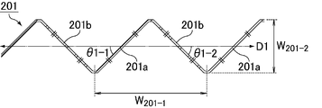
(7)また、本開示のある実施形態は、上記(2)の構成に加え、上記第一の方向と直交する方向における、上記複数の第一のバスラインの屈曲の幅の合計は、上記第一の方向と直交する方向における上記液晶表示パネルの表示領域の長さに対して、0.75倍以上、1.25倍以下であってもよい。 (7) Further, in an embodiment of the present disclosure, in addition to the configuration of (2) above, the total bending width of the plurality of first bus lines in the direction orthogonal to the first direction is It may be 0.75 times or more and 1.25 times or less the length of the display area of the liquid crystal display panel in the direction orthogonal to the first direction.
(8)また、本開示のある実施形態は、上記(2)の構成に加え、上記第二の方向と直交する方向における、上記複数の第二のバスラインの屈曲の幅の合計は、上記第二の方向と直交する方向における上記液晶表示パネルの表示領域の長さに対して、0.75倍以上、1.25倍以下であってもよい。 (8) Further, in an embodiment of the present disclosure, in addition to the configuration of (2) above, the total bending width of the plurality of second bus lines in the direction orthogonal to the second direction is It may be 0.75 times or more and 1.25 times or less the length of the display area of the liquid crystal display panel in the direction orthogonal to the second direction.
(9)また、本開示のある実施形態は、上記(2)の構成に加え、上記第一の方向と直交する方向における、上記複数の第一のバスラインの屈曲の幅の合計は、上記第一の方向と直交する方向における上記液晶表示パネルの表示領域の長さに対して、0.75倍以上、1.25倍以下であり、かつ、上記第二の方向と直交する方向における、上記複数の第二のバスラインの屈曲の幅の合計は、上記第二の方向と直交する方向における上記液晶表示パネルの表示領域の長さに対して、0.75倍以上、1.25倍以下であってもよい。 (9) Further, in an embodiment of the present disclosure, in addition to the configuration of (2) above, the total bending width of the plurality of first bus lines in the direction orthogonal to the first direction is 0.75 times or more and 1.25 times or less the length of the display area of the liquid crystal display panel in the direction perpendicular to the first direction, and in the direction perpendicular to the second direction, The total bending width of the plurality of second bus lines is 0.75 times or more and 1.25 times the length of the display area of the liquid crystal display panel in the direction perpendicular to the second direction. It may be below.
(10)また、本開示のある実施形態は、上記(2)の構成に加え、上記液晶表示パネルは、上記表示電極がそれぞれ配置された複数の表示単位を有し、上記第一のバスラインの屈曲周期は、上記第一の方向における一つの上記表示単位の最大長さの3倍以下であってもよい。 (10) Further, in an embodiment of the present disclosure, in addition to the configuration of (2) above, the liquid crystal display panel has a plurality of display units in which the display electrodes are respectively arranged, and the first bus line may be less than or equal to three times the maximum length of one display unit in the first direction.
(11)また、本開示のある実施形態は、上記(2)の構成に加え、上記液晶表示パネルは、上記表示電極がそれぞれ配置された複数の表示単位を有し、上記第二のバスラインの屈曲周期は、上記第二の方向における一つの上記表示単位の最大長さの3倍以下であってもよい。 (11) Further, in an embodiment of the present disclosure, in addition to the configuration of (2) above, the liquid crystal display panel has a plurality of display units in which the display electrodes are respectively arranged, and the second bus line may be less than or equal to three times the maximum length of one display unit in the second direction.
(12)また、本開示のある実施形態は、上記(2)の構成に加え、上記液晶表示パネルは、上記表示電極がそれぞれ配置された複数の表示単位を有し、上記第一のバスラインの屈曲周期は、上記第一の方向における一つの上記表示単位の最大長さの3倍以下であり、かつ、上記第二のバスラインの屈曲周期は、上記第二の方向における一つの上記表示単位の最大長さの3倍以下であってもよい。 (12) Further, in an embodiment of the present disclosure, in addition to the configuration of (2) above, the liquid crystal display panel has a plurality of display units in which the display electrodes are respectively arranged, and the first bus line is no more than three times the maximum length of one display unit in the first direction, and the bending period of the second bus line is one display unit in the second direction It may be less than or equal to three times the maximum length of the unit.
(13)また、本開示のある実施形態は、上記(2)の構成に加え、隣接する二本の上記第一のバスライン間の距離が変化し、上記隣接する二本の上記第一のバスライン間の距離が最も近くなる部分は、平面視において、上記表示電極と重なっていてもよい。 (13) Further, in an embodiment of the present disclosure, in addition to the configuration of (2) above, the distance between the two adjacent first bus lines is changed, and the two adjacent first bus lines are The portion where the distance between the bus lines is the shortest may overlap the display electrode in plan view.
(14)また、本開示のある実施形態は、上記(2)の構成に加え、隣接する二本の第二のバスライン間の距離が変化し、隣接する二本の第二のバスライン間の距離が最も近くなる部分は、平面視において、上記表示電極と重なっていてもよい。 (14) Further, in an embodiment of the present disclosure, in addition to the configuration of (2) above, the distance between two adjacent second bus lines is changed, and the distance between two adjacent second bus lines is may overlap the display electrodes in plan view.
(15)また、本開示のある実施形態は、上記(2)の構成に加え、上記液晶表示パネルは、上記表示電極がそれぞれ配置された複数の表示単位を有し、一つの第一のバスラインについて、上記第一の方向と直交する方向における屈曲の幅を短辺とし、上記第一の方向における上記一つの第一のバスラインの長さを長辺とする長方形の領域を上記一つの第一のバスラインの存在領域とすると、平面視において、隣接する二つの上記第一のバスラインの存在領域は重ならず、上記第一の方向と直交する方向に隣接する二つの上記第一のバスラインの存在領域の間隔は、上記第一の方向と直交する方向における、一つの前記表示単位の最大長さに対して、0.25倍以下であってもよい。 (15) Further, in an embodiment of the present disclosure, in addition to the configuration of (2) above, the liquid crystal display panel has a plurality of display units in which the display electrodes are respectively arranged, and one first bus With respect to the line, a rectangular area having a short side that is the width of the bend in the direction perpendicular to the first direction and a long side that is the length of the one first bus line in the first direction is the one Assuming that the existence area of the first bus line is the existence area of the first bus line, the existence areas of the two adjacent first bus lines do not overlap in a plan view, and the two adjacent first bus lines in the direction perpendicular to the first direction do not overlap each other. The interval between the bus line existing regions may be 0.25 times or less of the maximum length of one display unit in the direction orthogonal to the first direction.
(16)また、本開示のある実施形態は、上記(2)の構成に加え、上記液晶表示パネルは、上記表示電極がそれぞれ配置された複数の表示単位を有し、一つの第二のバスラインについて、上記第二の方向と直交する方向における屈曲の幅を短辺とし、上記第二の方向における上記一つの第二のバスラインの長さを長辺とする長方形の領域を上記一つの第二のバスラインの存在領域とすると、平面視において、隣接する二つの上記第二のバスラインの存在領域は重ならず、上記第二の方向と直交する方向に隣接する二つの上記第二のバスラインの存在領域の間隔は、上記第二の方向と直交する方向における、一つの前記表示単位の最大長さに対して、0.25倍以下であってもよい。 (16) Further, in an embodiment of the present disclosure, in addition to the configuration of (2) above, the liquid crystal display panel has a plurality of display units in which the display electrodes are respectively arranged, and one second bus Regarding the line, a rectangular area having a short side that is the width of the bend in the direction orthogonal to the second direction and a long side that is the length of the one second bus line in the second direction is the one Assuming that the existence area of the second bus line is an area where the two adjacent bus lines exist, in a plan view, the existing areas of the two adjacent second bus lines do not overlap, and the two adjacent areas of the second bus line in the direction perpendicular to the second direction are located in the same area. The interval between the bus line existing regions may be 0.25 times or less of the maximum length of one display unit in the direction perpendicular to the second direction.
(17)また、本開示のある実施形態は、上記(2)の構成に加え、上記液晶表示パネルは、上記表示電極がそれぞれ配置された複数の表示単位を有し、一つの第一のバスラインについて、上記第一の方向と直交する方向における屈曲の幅を短辺とし、上記第一の方向における上記一つの第一のバスラインの長さを長辺とする長方形の領域を上記一つの第一のバスラインの存在領域とし、一つの第二のバスラインについて、上記第二の方向と直交する方向における屈曲の幅を短辺とし、上記第二の方向における上記一つの第二のバスラインの長さを長辺とする長方形の領域を上記一つの第二のバスラインの存在領域とすると、平面視において、隣接する二つの上記第一のバスラインの存在領域は重ならず、かつ、隣接する二つの上記第二のバスラインの上記存在領域は、平面視において重ならず、上記第一の方向と直交する方向に隣接する二つの上記第一のバスラインの存在領域の間隔は、上記第一の方向と直交する方向における、一つの前記表示単位の最大長さに対して、0.25倍以下であり、上記第二の方向と直交する方向に隣接する二つの上記第二のバスラインの存在領域の間隔は、上記第二の方向と直交する方向における、一つの前記表示単位の最大長さに対して、0.25倍以下であってもよい。 (17) Further, in an embodiment of the present disclosure, in addition to the configuration of (2) above, the liquid crystal display panel has a plurality of display units in which the display electrodes are respectively arranged, and one first bus With respect to the line, a rectangular area having a short side that is the width of the bend in the direction perpendicular to the first direction and a long side that is the length of the one first bus line in the first direction is the one The area where the first bus line exists, and for one second bus line, the bending width in the direction perpendicular to the second direction is defined as the short side, and the one second bus in the second direction is defined as a short side. Assuming that a rectangular area having a long side equal to the length of the line is defined as an existing area of the second bus line, the existing areas of the two adjacent first bus lines do not overlap in plan view, and , the existing areas of the two adjacent second bus lines do not overlap in plan view, and the interval between the existing areas of the two first bus lines adjacent in the direction orthogonal to the first direction is , 0.25 times or less of the maximum length of one display unit in the direction perpendicular to the first direction, and the two second directions adjacent in the direction perpendicular to the second direction The interval between the bus line existing regions may be 0.25 times or less of the maximum length of one display unit in the direction perpendicular to the second direction.
(18)また、本開示のある実施形態は、上記(2)の構成に加え、上記液晶表示パネルは、上記表示電極がそれぞれ配置された複数の表示単位を有し、一つの第一のバスラインについて、上記第一の方向と直交する方向における屈曲の幅を短辺とし、上記第一の方向における上記一つの第一のバスラインの長さを長辺とする長方形の領域を上記一つの第一のバスラインの存在領域とすると、平面視において、隣接する二つの上記第一のバスラインの存在領域は重なり、上記第一の方向と直交する方向に隣接する二つの上記第一のバスラインの存在領域の重なり幅は、上記第一の方向と直交する方向における、一つの前記表示単位の最大長さに対して、0.25倍以下であってもよい。 (18) Further, in an embodiment of the present disclosure, in addition to the configuration of (2) above, the liquid crystal display panel has a plurality of display units in which the display electrodes are respectively arranged, and one first bus With respect to the line, a rectangular area having a short side that is the width of the bend in the direction perpendicular to the first direction and a long side that is the length of the one first bus line in the first direction is the one Assuming that the existence area of the first bus line is an existing area of the two adjacent first bus lines in a plan view, the two adjacent first bus lines in the direction perpendicular to the first direction overlap each other. The overlapping width of the line existing regions may be 0.25 times or less the maximum length of one display unit in the direction perpendicular to the first direction.
(19)また、本開示のある実施形態は、上記(2)の構成に加え、上記液晶表示パネルは、上記表示電極がそれぞれ配置された複数の表示単位を有し、一つの第二のバスラインについて、上記第二の方向と直交する方向における屈曲の幅を短辺とし、上記第二の方向における上記一つの第二のバスラインの長さを長辺とする長方形の領域を上記一つの第二のバスラインの存在領域とすると、平面視において、隣接する二つの上記第二のバスラインの存在領域は重なり、上記第二の方向と直交する方向に隣接する二つの上記第二のバスラインの存在領域の重なり幅は、上記第二の方向と直交する方向における、一つの前記表示単位の最大長さに対して、0.25倍以下であってもよい。 (19) Further, in an embodiment of the present disclosure, in addition to the configuration of (2) above, the liquid crystal display panel has a plurality of display units in which the display electrodes are respectively arranged, and one second bus Regarding the line, a rectangular area having a short side that is the width of the bend in the direction orthogonal to the second direction and a long side that is the length of the one second bus line in the second direction is the one Assuming that the existence area of the second bus line is an existing area of the second bus line, the existing area of the two adjacent second bus lines overlaps in plan view, and the two adjacent second bus lines in the direction orthogonal to the second direction are formed. The overlapping width of the line existing regions may be 0.25 times or less the maximum length of one display unit in the direction perpendicular to the second direction.
(20)また、本開示のある実施形態は、上記(2)の構成に加え、上記液晶表示パネルは、上記表示電極がそれぞれ配置された複数の表示単位を有し、一つの第一のバスラインについて、上記第一の方向と直交する方向における屈曲の幅を短辺とし、上記第一の方向における上記一つの第一のバスラインの長さを長辺とする長方形の領域を上記一つの第一のバスラインの存在領域とし、一つの第二のバスラインについて、上記第二の方向と直交する方向における屈曲の幅を短辺とし、上記第二の方向における上記一つの第二のバスラインの長さを長辺とする長方形の領域を上記一つの第二のバスラインの存在領域とすると、平面視において、隣接する二つの上記第一のバスラインの存在領域は重なり、かつ、隣接する二つの上記第二のバスラインの上記存在領域は、平面視において重なり、上記第一の方向と直交する方向に隣接する二つの上記第一のバスラインの存在領域の重なり幅は、上記第一の方向と直交する方向における、一つの前記表示単位の最大長さに対して、0.25倍以下であり、上記第二の方向と直交する方向に隣接する二つの上記第二のバスラインの存在領域の重なり幅は、上記第二の方向と直交する方向における、一つの前記表示単位の最大長さに対して、0.25倍以下であってもよい。 (20) Further, in an embodiment of the present disclosure, in addition to the configuration of (2) above, the liquid crystal display panel has a plurality of display units in which the display electrodes are respectively arranged, and one first bus With respect to the line, a rectangular area having a short side that is the width of the bend in the direction perpendicular to the first direction and a long side that is the length of the one first bus line in the first direction is the one The area where the first bus line exists, and for one second bus line, the bending width in the direction perpendicular to the second direction is defined as the short side, and the one second bus in the second direction is defined as a short side. Assuming that a rectangular region having a long side equal to the length of the line is defined as the existing region of the second bus line, the existing regions of the two adjacent first bus lines overlap and are adjacent to each other in a plan view. The existing regions of the two second bus lines overlap in plan view, and the overlapping width of the existing regions of the two first bus lines adjacent in the direction orthogonal to the first direction is the first Two second bus lines that are 0.25 times or less the maximum length of one display unit in a direction orthogonal to one direction and that are adjacent to each other in a direction orthogonal to the second direction may be 0.25 times or less the maximum length of one display unit in the direction perpendicular to the second direction.
(21)また、本開示のある実施形態は、上記(1)の構成に加え、上記液晶表示パネルは、上記表示電極がそれぞれ配置された複数の表示単位を有し、上記複数の第一のバスラインは、それぞれ複数の屈曲点を有し、隣接する上記第一のバスラインにおいて、最も近い上記屈曲点間の上記第一の方向と平行な距離は、上記第一の方向と直交する方向における、一つの上記表示単位の最大長さに対して、0.25倍以下であってもよい。 (21) Further, in an embodiment of the present disclosure, in addition to the configuration of (1) above, the liquid crystal display panel has a plurality of display units in which the display electrodes are respectively arranged, and the plurality of first Each of the bus lines has a plurality of bending points, and in the adjacent first bus lines, the distance parallel to the first direction between the nearest bending points is the direction orthogonal to the first direction. , may be 0.25 times or less of the maximum length of one of the above display units.
(22)また、本開示のある実施形態は、上記(1)の構成に加え、上記液晶表示パネルは、上記表示電極がそれぞれ配置された複数の表示単位を有し、上記複数の第二のバスラインは、それぞれ複数の屈曲点を有し、隣接する上記第二のバスラインにおいて、最も近い上記屈曲点間の上記第二の方向と平行な距離は、上記第二の方向と直交する方向における、一つの上記表示単位の最大長さに対して、0.25倍以下であってもよい。 (22) Further, in an embodiment of the present disclosure, in addition to the configuration of (1) above, the liquid crystal display panel has a plurality of display units in which the display electrodes are respectively arranged, and the plurality of second Each of the bus lines has a plurality of bending points, and in the adjacent second bus lines, the distance parallel to the second direction between the nearest bending points is the direction orthogonal to the second direction. , may be 0.25 times or less of the maximum length of one of the above display units.
(23)また、本開示のある実施形態は、上記(1)の構成に加え、上記液晶表示パネルは、上記表示電極がそれぞれ配置された複数の表示単位を有し、上記複数の第一のバスラインは、それぞれ複数の屈曲点を有し、隣接する上記第一のバスラインにおいて、最も近い上記屈曲点間の前記第一の方向と平行な距離は、上記第一の方向と直交する方向における、一つの上記表示単位の最大長さに対して、0.25倍以下であり、かつ、上記複数の第二のバスラインは、それぞれ複数の屈曲点を有し、隣接する上記第二のバスラインにおいて、最も近い上記屈曲点間の上記第二の方向と平行な距離は、上記第二の方向と直交する方向における、一つの上記表示単位の最大長さに対して、0.25倍以下であってもよい。 (23) Further, in an embodiment of the present disclosure, in addition to the configuration of (1) above, the liquid crystal display panel has a plurality of display units in which the display electrodes are respectively arranged, and the plurality of first Each of the bus lines has a plurality of bending points, and in the adjacent first bus lines, the distance parallel to the first direction between the nearest bending points is the direction orthogonal to the first direction. , is 0.25 times or less the maximum length of one of the display units, and the plurality of second bus lines each have a plurality of bending points, and the adjacent second bus lines In the bus line, the distance parallel to the second direction between the nearest bending points is 0.25 times the maximum length of one display unit in the direction orthogonal to the second direction. It may be below.
(24)また、本開示のある実施形態は、上記(1)の構成に加え、上記カラー表示素子が有する上記異なる色のサブ画素において、平面視で、サブ画素の開口領域の面積から、上記液晶表示パネルが有する上記複数の第一のバスライン及び上記複数の第二のバスラインと重なる面積を差し引いた面積をサブ画素実効透過面積とし、上記カラー表示素子の、上記行方向にN個分(Nは、2以上の整数)、上記列方向にN個分の領域に含まれるN2個の画素について、同じ色の上記サブ画素実効透過面積の総和を、同色実効透過面積とするとき、上記N2個の画素上に、上記行方向及び上記列方向に所定の幅で格子状に複数の測定点を設定し、上記カラー表示素子を固定した状態で、上記行方向及び上記列方向に沿って、上記液晶表示パネルを移動させ、上記測定点毎に上記同色実効透過面積を求めた場合に、各色の上記同色実効透過面積は、下記式(1)及び下記式(2)を満たしてもよい。
(SMax-SAve)÷SAve ≦ 0.25 (1)
(SAve-SMin)÷SAve ≦ 0.25 (2)
(上記SMaxは、上記測定点毎に求めた、上記同色実効透過面積の最大値であり、
上記SMinは、上記測定点毎に求めた、上記同色実効透過面積の最小値であり、
上記SAveは、上記測定点毎に求めた、上記同色実効透過面積の平均値である。)
(24) In addition to the configuration of (1) above, in an embodiment of the present disclosure, in the sub-pixels of the different colors included in the color display element, from the area of the opening regions of the sub-pixels in a plan view, the above The area obtained by subtracting the area overlapping with the plurality of first bus lines and the plurality of second bus lines of the liquid crystal display panel is defined as a sub-pixel effective transmission area, and N color display elements in the row direction. (N is an integer equal to or greater than 2), for N 2 pixels included in the N regions in the column direction, when the sum of the effective transmission areas of the sub-pixels of the same color is defined as the effective transmission area of the same color, On the N 2 pixels, a plurality of measurement points are set in a grid shape with a predetermined width in the row direction and the column direction, and with the color display element fixed, the measurement points are measured in the row direction and the column direction. When the liquid crystal display panel is moved along and the same-color effective transmission area is obtained for each of the measurement points, the same-color effective transmission area for each color satisfies the following formula (1) and the following formula (2). good too.
(S Max - S Ave )/S Ave ≤ 0.25 (1)
(S Ave −S Min )/S Ave ≤ 0.25 (2)
(The above S Max is the maximum value of the same color effective transmission area obtained for each measurement point,
The S Min is the minimum value of the effective transmission area of the same color obtained for each measurement point,
The above S Ave is the average value of the same-color effective transmission areas obtained for each of the above measurement points. )
(25)また、本開示のある実施形態は、上記(24)の構成に加え、各色の上記同色実効透過面積は、下記式(3)及び下記式(4)を満たしてもよい。
(SMax - SAve)÷ SAve ≦ 0.1 (3)
(SAve - SMin)÷ SAve ≦ 0.1 (4)
(25) Further, in an embodiment of the present disclosure, in addition to the configuration of (24) above, the same-color effective transmission area of each color may satisfy the following formulas (3) and (4).
(S Max - S Ave )/S Ave ≤ 0.1 (3)
(S Ave - S Min )/S Ave ≤ 0.1 (4)
(26)また、本開示のある実施形態は、上記(1)の構成に加え、上記液晶表示パネルは、上記表示電極がそれぞれ配置された複数の表示単位を有し、一つの表示単位の面積は、上記カラー表示素子に含まれる一つの画素の面積よりも大きくてもよい。 (26) Further, in an embodiment of the present disclosure, in addition to the configuration of (1) above, the liquid crystal display panel has a plurality of display units in which the display electrodes are respectively arranged, and the area of one display unit may be larger than the area of one pixel included in the color display element.
(27)また、本開示のある実施形態は、上記(1)の構成に加え、上記カラー表示素子に含まれる上記サブ画素毎に配置された画素電極の外縁は、少なくとも一つの直線部分を含み、平面視において、上記画素電極の直線部分の延伸方向は、上記液晶表示パネルに含まれる上記表示電極の外縁を構成する全ての辺の延伸方向と交差してもよい。 (27) Further, in an embodiment of the present disclosure, in addition to the configuration of (1) above, the outer edge of the pixel electrode arranged for each of the sub-pixels included in the color display element includes at least one linear portion. In a plan view, the extending direction of the linear portion of the pixel electrode may intersect with the extending directions of all the sides forming the outer edge of the display electrode included in the liquid crystal display panel.
(28)また、本開示のある実施形態は、上記(27)の構成に加え、上記画素電極の直線部分の延伸方向と、上記表示電極の外縁を構成する少なくとも一つの辺の延伸方向とのなす角は、30°以上、60°以下であってもよい。 (28) Further, in an embodiment of the present disclosure, in addition to the configuration of (27) above, the extending direction of the linear portion of the pixel electrode and the extending direction of at least one side forming the outer edge of the display electrode The angle to be formed may be 30° or more and 60° or less.
(29)また、本開示のある実施形態は、上記(1)の構成に加え、上記表示電極の形状は、四角形であってもよい。 (29) Further, in an embodiment of the present disclosure, in addition to the configuration of (1) above, the shape of the display electrodes may be square.
(30)また、本開示のある実施形態は、上記(1)の構成に加え、上記表示電極の形状は、長方形であってもよい。 (30) Further, in an embodiment of the present disclosure, in addition to the configuration of (1) above, the shape of the display electrode may be rectangular.
(31)また、本開示のある実施形態は、上記(30)の構成に加え、上記表示電極の形状は、長方形であり、長辺の長さが、短辺の長さの1.5倍以上、2.5倍以下であってもよい。 (31) Further, in an embodiment of the present disclosure, in addition to the configuration of (30) above, the shape of the display electrode is rectangular, and the length of the long side is 1.5 times the length of the short side. It may be greater than or equal to 2.5 times or less.
(32)また、本開示のある実施形態は、上記(1)の構成に加え、平面視において、上記複数の第一のバスラインの少なくとも一つは、上記複数の表示電極の少なくとも一つと重なる第一の電極重畳部を含んでもよい。 (32) Further, in an embodiment of the present disclosure, in addition to the configuration (1) above, at least one of the plurality of first bus lines overlaps with at least one of the plurality of display electrodes in plan view. A first electrode overlap may be included.
(33)また、本開示のある実施形態は、上記(32)の構成に加え、一本の第一のバスラインにおける上記第一の電極重畳部の合計は、上記一本の第一のバスラインの全長に対して、75%以上であってもよい。 (33) Further, in an embodiment of the present disclosure, in addition to the configuration of (32) above, the total of the first electrode overlapping portions in one first bus line is It may be 75% or more of the total length of the line.
(34)また、本開示のある実施形態は、上記(1)の構成に加え、平面視において、上記複数の第二のバスラインの少なくとも一つは、上記複数の表示電極の少なくとも一つと重なる第二の電極重畳部を含んでもよい。 (34) Further, in an embodiment of the present disclosure, in addition to the configuration (1) above, at least one of the plurality of second bus lines overlaps with at least one of the plurality of display electrodes in plan view. A second electrode overlap may be included.
(35)また、本開示のある実施形態は、上記(34)の構成に加え、一本の第二のバスラインにおける上記第二の電極重畳部の合計は、上記一本の第二のバスラインの全長に対して、75%以上であってもよい。 (35) Further, in an embodiment of the present disclosure, in addition to the configuration of (34) above, the total of the second electrode overlapping portions in one second bus line is It may be 75% or more of the total length of the line.
(36)また、本開示のある実施形態は、上記(1)の構成に加え、平面視において、上記複数の第一のバスラインの少なくとも一つは、上記複数の表示電極の少なくとも一つと重なる第一の電極重畳部を含み、かつ、平面視において、上記複数の第二のバスラインの少なくとも一つは、上記複数の表示電極の少なくとも一つと重なる第二の電極重畳部を含んでもよい。 (36) Further, in an embodiment of the present disclosure, in addition to the configuration (1) above, at least one of the plurality of first bus lines overlaps at least one of the plurality of display electrodes in plan view. At least one of the plurality of second bus lines including the first electrode overlapping portion may include a second electrode overlapping portion overlapping at least one of the plurality of display electrodes in plan view.
(37)また、本開示のある実施形態は、上記(36)の構成に加え、一本の第一のバスラインにおける上記第一の電極重畳部の合計は、上記一本の第一のバスラインの全長に対して、75%以上であり、かつ、一本の第二のバスラインにおける上記第二の電極重畳部の合計は、上記一本の第二のバスラインの全長に対して、75%以上であってもよい。 (37) Further, in an embodiment of the present disclosure, in addition to the configuration of (36) above, the total of the first electrode overlapping portions in one first bus line is 75% or more of the total length of the line, and the total of the second electrode overlapping portions in the single second bus line is, with respect to the total length of the single second bus line, It may be 75% or more.
(38)また、本開示のある実施形態は、上記(1)の構成に加え、上記液晶表示パネルが有する上記TFT基板は、支持基材と上記第一のバスラインと、第一の絶縁層と、上記第二のバスラインと、第二の絶縁層と、上記表示電極の順で配置されてもよい。 (38) Further, in an embodiment of the present disclosure, in addition to the configuration of (1) above, the TFT substrate included in the liquid crystal display panel includes a supporting base material, the first bus line, and a first insulating layer. , the second bus line, the second insulating layer, and the display electrode may be arranged in this order.
(39)また、本開示のある実施形態は、上記(38)の構成に加え、上記第二の絶縁層と上記表示電極との間に、上記第二の絶縁層側から、透明な導電体層と、第三の絶縁層とを有してもよい。 (39) In addition to the configuration of (38) above, an embodiment of the present disclosure includes, from the second insulating layer side, a transparent conductor between the second insulating layer and the display electrode: and a third insulating layer.
(40)また、本開示のある実施形態は、上記(39)の構成に加え、平面視において、上記第一のバスラインは、上記複数の表示電極の少なくとも一つと重なる第一の電極重畳部を含み、上記透明な導電体層は、上記第一の電極重畳部と重なるように配置されてもよい。 (40) Further, in an embodiment of the present disclosure, in addition to the configuration of (39) above, in a plan view, the first bus line has a first electrode overlapping portion that overlaps at least one of the plurality of display electrodes. and the transparent conductor layer may be arranged so as to overlap the first electrode overlapping portion.
(41)また、本開示のある実施形態は、上記(39)の構成に加え、平面視において、上記第二のバスラインは、上記複数の表示電極の少なくとも一つと重なる第二の電極重畳部を含み、上記透明な導電体層は、上記第二の電極重畳部と重なるように配置されてもよい。 (41) Further, in an embodiment of the present disclosure, in addition to the configuration of (39) above, in a plan view, the second bus line has a second electrode overlapping portion that overlaps at least one of the plurality of display electrodes. and the transparent conductor layer may be arranged so as to overlap the second electrode overlapping portion.
(42)また、本開示のある実施形態は、上記(39)の構成に加え、平面視において、上記複数の第一のバスラインの少なくとも一つは、上記複数の表示電極の少なくとも一つと重なる第一の電極重畳部を含み、上記複数の第二のバスラインの少なくとも一つは、上記複数の表示電極の少なくとも一つと重なる第二の電極重畳部を含み、上記透明な導電体層は、上記第一及び第二の電極重畳部と重なってもよい。 (42) Further, in an embodiment of the present disclosure, in addition to the configuration of (39) above, at least one of the plurality of first bus lines overlaps at least one of the plurality of display electrodes in plan view. including a first electrode overlapping portion, at least one of the plurality of second bus lines including a second electrode overlapping portion overlapping at least one of the plurality of display electrodes, the transparent conductor layer comprising: It may overlap with the first and second electrode overlapping portions.
(43)また、本開示のある実施形態は、上記(1)の構成に加え、上記液晶表示パネルは、平面視において、隣接する表示電極の間に遮光部材を有さなくてもよい。 (43) Further, in an embodiment of the present disclosure, in addition to the configuration of (1) above, the liquid crystal display panel does not need to have a light shielding member between adjacent display electrodes in plan view.
(44)また、本開示のある実施形態は、上記(1)の構成に加え、表示装置全体の白表示でのヘイズ値は、79%以下であってもよい。 (44) In addition to the configuration of (1) above, an embodiment of the present disclosure may have a haze value of 79% or less in white display of the entire display device.
(45)また、本開示のある実施形態は、上記(1)の構成に加え、表示装置全体の白表示でのヘイズ値は、50%以下であってもよい。 (45) In addition to the configuration of (1) above, an embodiment of the present disclosure may have a haze value of 50% or less in white display of the entire display device.
(46)また、本開示のある実施形態は、上記(1)の構成に加え、上記液晶表示パネルが有する上記液晶層を、第一の液晶層とすると、上記カラー表示素子は、一対の基板に挟持された第二の液晶層を有する液晶素子であり、第一の偏光板、上記カラー表示素子、第二の偏光板、上記液晶表示パネル、第三の偏光板の順で積層されてもよい。 (46) Further, in an embodiment of the present disclosure, in addition to the configuration of (1) above, when the liquid crystal layer included in the liquid crystal display panel is a first liquid crystal layer, the color display element includes a pair of substrates A liquid crystal element having a second liquid crystal layer sandwiched between the first polarizing plate, the color display element, the second polarizing plate, the liquid crystal display panel, and the third polarizing plate. good.
(47)また、本開示のある実施形態は、上記(1)の構成に加え、上記液晶表示パネルが有する上記液晶層を、第一の液晶層とすると、上記カラー表示素子は、カラーフィルタを有するカラーフィルタ基板と、第二の液晶層とを有する液晶素子であり、上記第二の液晶層は、上記カラーフィルタ基板と、上記液晶表示パネルの上記対向基板とに挟持され、第一の偏光板、上記カラーフィルタ基板、上記第二の液晶層、偏光層、上記対向基板、第一の液晶層、上記TFT基板、第二の偏光板をこの順に有し、上記対向基板は、上記偏光層側の表面に、上記第二の液晶層に印加する電圧を調整するための複数のスイッチング素子を有してもよい。 (47) Further, in an embodiment of the present disclosure, in addition to the configuration (1) above, when the liquid crystal layer of the liquid crystal display panel is a first liquid crystal layer, the color display element includes a color filter. and a second liquid crystal layer, wherein the second liquid crystal layer is sandwiched between the color filter substrate and the counter substrate of the liquid crystal display panel, and the first polarized light a plate, the color filter substrate, the second liquid crystal layer, a polarizing layer, the counter substrate, the first liquid crystal layer, the TFT substrate, and the second polarizing plate in this order, and the counter substrate includes the polarizing layer The side surface may have a plurality of switching elements for adjusting the voltage applied to the second liquid crystal layer.
(48)また、本開示のある実施形態は、上記(1)の構成に加え、上記液晶表示パネルがフロントパネル、上記カラー表示素子がリアパネルであり、上記液晶表示パネルが有する上記液晶層を、第一の液晶層とすると、上記カラー表示素子は、一対の基板に挟持された第二の液晶層を有する液晶素子であり、上記一対の基板のうち、表示装置の背面側に位置する基板は、上記第二の液晶層と対向する側に反射部材を有してもよい。 (48) Further, in an embodiment of the present disclosure, in addition to the configuration of (1) above, the liquid crystal display panel is a front panel, the color display element is a rear panel, and the liquid crystal layer of the liquid crystal display panel includes: Assuming that the first liquid crystal layer is the first liquid crystal layer, the color display element is a liquid crystal element having a second liquid crystal layer sandwiched between a pair of substrates. , a reflecting member may be provided on a side facing the second liquid crystal layer.
(49)また、本開示のある実施形態は、上記(47)又は(48)の構成に加え、上記液晶表示パネルは、上記表示電極がそれぞれ配置された複数の表示単位を有し、上記表示装置の厚み方向における、上記第一の液晶層と、上記第二の液晶層との間隔は、上記第一の方向又は上記第二の方向における、一つの前記表示単位の最大長さのうち長い方にして、0.1倍以上であってもよい。 (49) Further, in an embodiment of the present disclosure, in addition to the configuration of (47) or (48) above, the liquid crystal display panel has a plurality of display units in which the display electrodes are respectively arranged, and the display The distance between the first liquid crystal layer and the second liquid crystal layer in the thickness direction of the device is longer than the maximum length of one display unit in the first direction or the second direction. On the other hand, it may be 0.1 times or more.
(50)また、本開示のある実施形態は、上記(1)の構成に加え、上記カラー表示素子がフロントパネル、上記液晶表示パネルがリアパネルであり、上記カラー表示素子、上記液晶表示パネル、バックライトの順に配置されてもよい。 (50) Further, in an embodiment of the present disclosure, in addition to the configuration of (1) above, the color display element is a front panel, the liquid crystal display panel is a rear panel, and the color display element, the liquid crystal display panel, and the back They may be arranged in order of light.
(51)また、本開示のある実施形態は、上記(1)の構成に加え、上記液晶表示パネルがフロントパネル、上記カラー表示素子がリアパネルであり、上記液晶表示パネル、上記カラー表示素子、バックライトの順に配置されてもよい。 (51) Further, in an embodiment of the present disclosure, in addition to the configuration of (1) above, the liquid crystal display panel is a front panel, the color display element is a rear panel, and the liquid crystal display panel, the color display element, the back panel They may be arranged in order of light.
(52)また、本開示のある実施形態は、上記(1)の構成に加え、上記液晶表示パネルが有する上記対向基板は、カラーフィルタを有してもよい。 (52) Further, in an embodiment of the present disclosure, in addition to the configuration (1) above, the counter substrate included in the liquid crystal display panel may have a color filter.
(53)また、本開示のある実施形態は、上記(50)又は(51)の構成に加え、
上記バックライトは、複数色の発光素子を含み、上記複数色の発光素子が、時分割で点灯されるフィールドシーケンシャル方式で駆動されることで、上記液晶表示パネルがカラー表示されてもよい。
(54)また、本開示のある実施形態は、上記(1)の構成に加え、上記液晶表示パネルがフロントパネル、上記カラー表示素子がリアパネルであり、上記カラー表示素子は、発光層を有してもよい。
(55)また、本開示のある実施形態は、上記(54)の構成に加え、上記液晶表示パネルは、上記表示電極がそれぞれ配置された複数の表示単位を有し、上記表示装置の厚み方向における、上記液晶層と、上記発光層との間隔は、上記第一の方向又は上記第二の方向における、一つの前記表示単位の最大長さのうち長い方にして、0.1倍以上であってもよい。
(53) Further, in an embodiment of the present disclosure, in addition to the configuration of (50) or (51) above,
The backlight may include light-emitting elements of a plurality of colors, and the liquid crystal display panel may display colors by driving the light-emitting elements of the plurality of colors by a field sequential system in which the light-emitting elements are illuminated in a time division manner.
(54) Further, in an embodiment of the present disclosure, in addition to the configuration of (1) above, the liquid crystal display panel is a front panel, the color display element is a rear panel, and the color display element has a light-emitting layer. may
(55) Further, in an embodiment of the present disclosure, in addition to the configuration of (54) above, the liquid crystal display panel has a plurality of display units in which the display electrodes are respectively arranged, and the thickness direction of the display device is 3, the distance between the liquid crystal layer and the light-emitting layer is 0.1 times or more of the maximum length of one display unit in the first direction or the second direction, whichever is longer. There may be.
本開示によれば、表示画面の全面に対してモアレの発生が抑制され、かつ、透過率が高いデュアルセルの表示装置を提供することができる。 According to the present disclosure, it is possible to provide a dual-cell display device that suppresses the occurrence of moire over the entire display screen and has high transmittance.
以下、本開示の実施形態に係る表示装置について説明する。本開示は、以下の実施形態に記載された内容に限定されるものではなく、本開示の構成を充足する範囲内で、適宜設計変更を行うことが可能である。また、同様の構成を有する部材については、同じ符号を付し、重複する説明は省略する。 A display device according to an embodiment of the present disclosure will be described below. The present disclosure is not limited to the contents described in the following embodiments, and design changes can be made as appropriate within the scope of satisfying the configuration of the present disclosure. Also, members having the same configuration are denoted by the same reference numerals, and overlapping descriptions are omitted.
<実施形態1>
(表示装置)
図1は、実施形態1に係る表示装置の断面模式図である。図1に示したように、実施形態1に係る表示装置1は、カラー表示素子100と、カラー表示素子100に積層された液晶表示パネル200とを備える。カラー表示素子100、液晶表示パネル200のいずれが観察者側に配置されてもよいが、図1では、カラー表示素子100がフロントパネル、液晶表示パネル200がリアパネルである場合を例示した。表示装置1は、カラー表示素子100、液晶表示パネル200、バックライト300の順に配置される。
<
(Display device)
FIG. 1 is a schematic cross-sectional view of a display device according to
表示装置1は、デュアルセルディスプレイであり、入力信号に応じて、フロントパネルに表示する映像と、リアパネルに表示する映像を生成する、Dual Cell信号処理システムを備える。入力映像信号に基づいて、Dual Cell信号処理が行われ、カラー表示素子100、液晶表示パネル200には、それぞれ異なるタイミングコントローラー(TCON)から、画像信号が入力され、バックライト300には、バックライト駆動回路から点灯信号が入力される。カラー表示素子100をフロントパネル、液晶表示パネル200をリアパネルとし、カラー表示素子100に表示される映像に対して、背面から上記画像の輝度を調整するように、液晶表示パネル200を調光パネルとして用いることで、コントラストの高い表示を行うことができる。
The
表示装置1は、第一の偏光板10、カラー表示素子100、第二の偏光板20、液晶表示パネル200、第三の偏光板30の順で積層されている。カラー表示素子100と液晶表示パネル200とで第二の偏光板20を共有する。表示装置1では、図45に示した拡散OCA2050の代わりに、透明度の高いOCA40を用いている。透明度の高いOCA40を用いることで、OCA40を透過する際の偏光状態の変化、偏光解消等の悪影響を少なくできるため、図45に示した従来のデュアルセルディスプレイが有するリアパネル2200側の第三の偏光板2030に相当する部材を取り除くことができる。実施例1では第三の偏光板2030を取り除いている。偏光板一枚と、拡散OCAを有さないことで、従来のデュアルセルディスプレイよりも透過率を向上させることができる。透明度の高いOCA40は、例えば、ヘイズ値が79%以下である粘着シートである。
In the
第二の偏光板20と透明度の高いOCA40は接していてもよい。また、透明度の高いOCA40と液晶表示パネル200(図1では対向基板230)とが接していてもよい。
The second
第一の偏光板10、第二の偏光板20及び第三の偏光板30は、直線偏光板であることが好ましい。上記直線偏光板としては、特に限定されず、液晶表示装置の分野において従来公知のものを用いることができる。第一の偏光板10の透過軸と第二の偏光板20の透過軸、第二の偏光板20の透過軸と第三の偏光板30の透過軸はともに、クロスニコルに配置されることが好ましい。
The first
表示装置1は、モアレの発生を抑制できることから、従来の表示装置のように、カラー表示素子100と液晶表示パネル200の間に拡散OCAを配置する必要がない。拡散OCAを配置しない構成としては、表示装置1全体の白表示でのヘイズ値は79%以下であることが好ましく、50%以下であることがより好ましい。上記白表示とは、最も高い階調で表示した場合をいう。
Since the
<ヘイズ値の検討>
異なるOCAシートA~Eを用いた拡散層のヘイズ値、全光線透過率を測定した。上記全光線透過率とは、平行光(拡散せず直進する光)と拡散光を合計した光、すなわち、全方位に広がる光に対する透過率を指す。ヘイズ値、全光線透過率、平行光の透過率(完全平行光線透過率)、拡散光の透過率(拡散光透過率)の関係は、下記式(A)~(C)で表される。なお、ヘイズ及び全光線透過率は、例えば、日本電色工業社製の濁度計「HazeMeter NDH2000」等を用いて測定される。ヘイズは、JIS K 7136に準拠した方法で測定される。全光線透過率は、JIS K 7361-1に準拠した方法で測定される。
ヘイズ値=拡散光線透過率÷全光線透過率 (A)
全光線透過率=拡散光線透過率+完全平行光線透過率 (B)
完全平行光線透過率=全光線透過率×(1-ヘイズ値) (C)
<Consideration of haze value>
The haze value and total light transmittance of diffusion layers using different OCA sheets A to E were measured. The above-mentioned total light transmittance refers to the transmittance of light that is the sum of parallel light (light that travels straight without being diffused) and diffused light, that is, light that spreads in all directions. The relationship between the haze value, total light transmittance, parallel light transmittance (perfect parallel light transmittance), and diffuse light transmittance (diffuse light transmittance) is expressed by the following formulas (A) to (C). The haze and total light transmittance are measured using, for example, a turbidity meter "HazeMeter NDH2000" manufactured by Nippon Denshoku Industries Co., Ltd. A haze is measured by the method based on JISK7136. The total light transmittance is measured according to JIS K 7361-1.
Haze value = diffuse light transmittance / total light transmittance (A)
Total light transmittance = diffuse light transmittance + perfect parallel light transmittance (B)
Complete parallel light transmittance = total light transmittance x (1-haze value) (C)
ここで、表示装置を透過する光の透過率を考える場合には、バックライトから射出される光にある程度の広がりがあること、測定機器の受光器の取り込み角度にもある程度の広がりがあること、拡散層の配光分布等を考慮する必要があり、上記拡散層の完全平行光線透過率から、表示装置を透過する光の透過率を予想することは困難である。そこで、本発明者は、以下に示した表示装置を透過する光の透過率を測定する方法と同様の方法で、拡散層の透過率を測定した。本明細書中、表示装置を透過する光の透過率を測定する方法と同様の方法で測定した拡散層の透過率を、「略平行光線透過率」ともいう。 Here, when considering the transmittance of light passing through the display device, the light emitted from the backlight must be spread to some extent, the angle of acceptance of the light receiver of the measuring instrument must be spread to some extent, It is necessary to consider the light distribution and the like of the diffusion layer, and it is difficult to predict the transmittance of light passing through the display device from the complete parallel light transmittance of the diffusion layer. Therefore, the inventors measured the transmittance of the diffusion layer by a method similar to the method for measuring the transmittance of light transmitted through the display device described below. In this specification, the transmittance of the diffusion layer measured by a method similar to the method for measuring the transmittance of light transmitted through the display device is also referred to as "substantially parallel light transmittance."
(略平行光線透過率の測定方法)
以下に図49及び図50を用いて、略平行光線透過率の測定方法を説明する。図49は、略平行光線透過率の測定方法について説明した第一の模式図である。図50は、略平行光線透過率の測定方法について説明した第二の模式図である。まず、図49に示したように、バックライト300上にガラス基板111を配置した状態で、ガラス基板111のバックライト300と反対側から、光量測定器400により透過光量を測定し、得られた値をT_Refとする。
(Method for measuring approximately parallel light transmittance)
A method for measuring the approximately parallel light transmittance will be described below with reference to FIGS. 49 and 50. FIG. FIG. 49 is a first schematic diagram explaining the method of measuring the approximately parallel light transmittance. FIG. 50 is a second schematic diagram explaining the method of measuring the approximately parallel light transmittance. First, as shown in FIG. 49, with the
バックライト300は、本願の実施形態で用いるような、液晶表示装置の分野において従来公知のバックライトである。支持基材111は、カラー表示素子100及び液晶表示パネル200のカラーフィルタ基板やTFT基板の支持基材に用いられるものと同様であり、例えば、ガラス板が用いられる。光量測定器400は、液晶パネルの評価に用いられる測定器であり、例えば、コニカミノルタ製のCA310等を用いることができる。
The
次に、図50に示したように、OCAシートA~Eをそれぞれ拡散層1040として、二枚の上記ガラス板(支持基材111)を貼り合わせ、透過率評価用のサンプルを作成する。透過率評価用の各サンプルをバックライト300の上に配置し、光量測定器400により透過光量を測定し、得られた値を各サンプルの透過光量T_Sampleとする。略平行光線透過率は、下記式(D)で表される。
略平行光線透過率=T_Sample/T_Ref (D)
Next, as shown in FIG. 50, each of the OCA sheets A to E is used as a diffusion layer 1040, and the two glass plates (supporting substrate 111) are adhered to prepare a sample for transmittance evaluation. Each sample for transmittance evaluation is placed on the
Approximate parallel light transmittance = T_Sample/T_Ref (D)
<モアレの視認状況の検討>
図45~図48に示した従来のデュアルセルディスプレイについて、フロントパネル2100とリアパネル2200との間に、異なる拡散層を挟んだ検討例1~6のモアレの視認状況を検討した。検討例1は、フロントパネル2100とリアパネル2200との間に拡散層を設けない例である。検討例2~6は、拡散層として、それぞれOCAシートA~Eを用いた例である。
<Study of visibility of moire>
Regarding the conventional dual-cell display shown in FIGS. 45 to 48, the visibility of moire in Examples 1 to 6 in which different diffusion layers are sandwiched between the
検討例1~6の従来のデュアルセルディスプレイについて、ディスプレイを白表示とし、おおよそ1m離れた距離から正面を含めあらゆる方向から目視にてモアレの視認状況を評価した。下記表中、モアレが視認されない場合を○、モアレが僅かに視認される場合を△、モアレがはっきりと視認される場合を×とした。 Regarding the conventional dual-cell displays of Examination Examples 1 to 6, the display was set to display white, and the visibility of moire was evaluated visually from all directions including the front from a distance of about 1 m. In the table below, the case where moire was not visually recognized was evaluated as ◯, the case where moire was slightly visually observed as Δ, and the case where moire was clearly visually observed was evaluated as ×.
拡散層のヘイズ値、全光線透過率、完全平行光線透過率、略平行光線透過率及び検討例1~6のモアレの視認状況を、下記表1にまとめた。なお、検討例1については、拡散層としてOCAシートを用いないため、T_Sampleの値はT_Refと同じ値とする。 The haze value, total light transmittance, complete parallel light transmittance, substantially parallel light transmittance of the diffusion layer, and moiré visibility in Examination Examples 1 to 6 are summarized in Table 1 below. Note that, in Study Example 1, the value of T_Sample is the same value as T_Ref because the OCA sheet is not used as the diffusion layer.

モアレの視認状況について、表1の検討例5、6の結果から、拡散層のヘイズ値を88%以上とすることで、モアレを解消できることが確認された。すなわち、拡散層のみでモアレ対策を行う場合には、ヘイズ値が88%以上の拡散層を設ける必要があることが分かる。一方で、検討例1~3の結果から、従来のデュアルセルディスプレイでは、拡散層を設けても、拡散層のヘイズ値が79%以下であれば、モアレは抑制できないことが確認された。 From the results of Investigation Examples 5 and 6 in Table 1, it was confirmed that moire can be eliminated by setting the haze value of the diffusion layer to 88% or more. In other words, it can be seen that a diffusion layer having a haze value of 88% or more must be provided when moire countermeasures are to be taken only with a diffusion layer. On the other hand, from the results of Examination Examples 1 to 3, it was confirmed that moire cannot be suppressed in a conventional dual-cell display even if a diffusion layer is provided, provided that the haze value of the diffusion layer is 79% or less.
以下に、ヘイズ値と全光線透過率、ヘイズ値と完全平行光線透過率、及びヘイズ値と略平行光線透過率の関係を検討した。図51は、拡散層のヘイズ値と全光線透過率との関係を示したグラフである。図52は、拡散層のヘイズ値と完全平行光線透過率との関係を示したグラフである。図53は、拡散層のヘイズ値と略平行光線透過率との関係を示したグラフである。 The relationships between the haze value and the total light transmittance, the haze value and the complete parallel light transmittance, and the haze value and the substantially parallel light transmittance are examined below. FIG. 51 is a graph showing the relationship between the haze value of the diffusion layer and the total light transmittance. FIG. 52 is a graph showing the relationship between the haze value of the diffusion layer and the complete parallel light transmittance. FIG. 53 is a graph showing the relationship between the haze value of the diffusion layer and the approximately parallel light transmittance.
図51に示したように、拡散層のヘイズ値と拡散層の全光線透過率には相関関係がないことが確認された。一方で、図52に示したように、拡散層のヘイズ値が高くなるほど、拡散層の完全平行光線透過率が低くなることが確認された。更に、特筆すべきは、図53に示したように、拡散層のヘイズ値が高くなると、拡散層の略平行光線透過率が低下するが、特に、ヘイズ値が検討例3を境界としての78.8%を超えると、急激に略平行光線透過率が低下することが確認された。 As shown in FIG. 51, it was confirmed that there is no correlation between the haze value of the diffusion layer and the total light transmittance of the diffusion layer. On the other hand, as shown in FIG. 52, it was confirmed that the higher the haze value of the diffusion layer, the lower the complete parallel light transmittance of the diffusion layer. Furthermore, it should be noted that, as shown in FIG. 53, when the haze value of the diffusion layer increases, the transmittance of the diffusion layer decreases. It was confirmed that when the content exceeds 0.8%, the transmittance of substantially parallel rays is rapidly lowered.
図53の結果を、表1に示したモアレの視認状況と合わせて考えると、拡散層のヘイズ値を79%以下とすることで、急激なパネル透過率(略平行光線透過率)の低下を回避することができることが確認された。一方で、上述のように、従来のデュアルセルディスプレイでは、拡散層のヘイズが79%以下では、モアレの発生を抑制できない。しかしながら、実施形態1に係る表示装置1の構成では、モアレが視認されないため、例えば、ヘイズ値が79%以下である透明度の高いOCAを用いることができ、モアレの抑制と透過率の向上とを両立することができる。
Considering the results of FIG. 53 together with the visibility of moire shown in Table 1, it can be seen that by setting the haze value of the diffusion layer to 79% or less, a rapid drop in the panel transmittance (substantially parallel light transmittance) can be prevented. It has been confirmed that this can be avoided. On the other hand, as described above, in the conventional dual-cell display, when the haze of the diffusion layer is 79% or less, moire generation cannot be suppressed. However, in the configuration of the
カラー表示素子100と液晶表示パネル200とは接着しても、しなくてもよいが、接着することが好ましい。カラー表示素子100と液晶表示パネル200とを接着することで、図1に示したTFT基板110、対向基板230等の基材であるガラス基板と、空気層との界面反射がなくなり、透過率を高くできるためである。また、カラー表示素子100と液晶表示パネル200とを接着することで、熱によりカラー表示素子100又は液晶表示パネル200が反ったり、物理的な衝撃が加わったりした場合でも、カラー表示素子100の画素と液晶表示パネル200の表示単位との位置ずれを防ぐことができる。
The
カラー表示素子100と液晶表示パネル200とを貼り合わす場合、透明度の高いOCA、拡散OCAのいずれを用いてもよいが、透過率の向上、コスト抑制の観点からは、透明度の高いOCAを用いることが好ましい。また、カラー表示素子100と液晶表示パネル200との間に偏光板が一枚であると、カラー表示素子100、液晶表示パネル200のいずれか一方から紫外線を照射することで、効率よく紫外線をOCAに到達させることができるため、UV硬化タイプのOCAを用いることができ、短時間での硬化が可能となる。カラー表示素子100と液晶表示パネル200とを貼り合わさない場合、拡散シートを用いてもよい。なお、上述のように、表示装置1は、図45に示した従来のデュアルセルディスプレイが有するリアパネル2200側の第三の偏光板2030を削除している。これは、フロントパネル2100側の第二の偏光板2020を削除するよりも、リアパネル2200側の第三の偏光板2030を削除した方が、透明度の高いOCA等の僅かな偏光解消、散乱の影響を受けないため、高コントラストを得ることができるためである。
When the
バックライト300としては、特に限定されず、液晶表示装置の分野において従来公知のものを用いてもよく、例えば、直下型のバックライトでもよいし、エッジ型のバックライトでもよい。バックライト300を、全面一律に発光させてもよいし、バックライトの発光面を複数の点灯エリアに分けて部分駆動するローカルディミング駆動してもよい。直下型のバックライトをローカルディミング駆動することで、コントラストを更に向上させることができる。また、バックライト300は、複数色の発光素子を含み、上記複数色の発光素子が、時分割で点灯されるフィールドシーケンシャル方式で駆動されることで、液晶表示パネル200がカラー表示されてもよい。更に、動画をより鮮明に表示するために、バックライト300の全体又は一部分を周期的に点滅させてもよい。このような表示方法は、黒挿入、インパルス駆動等とも呼ばれ、具体的には、フレームレート(例えば120Hz)に同期して、バックライト300を消灯させることで動画表示性能を高めることができる。
The
以下に、実施形態1に係る表示装置と従来のデュアルセルディスプレイの透過率及びコントラスト(CR)を比較した。下記表2、表3は、それぞれ、従来のデュアルセルディスプレイと実施形態1に係る表示装置の透過率、白輝度、黒輝度、CRをまとめた表である。なお、従来のデュアルセルディスプレイは、図45に示した構成を有し、リアパネルとして図47に示した構成を有する液晶表示パネルを用いた。実施形態1に係る表示装置の一例として、図1に示した構成を有し、リアパネルとして後述する図4及び図5で示した構成を有する液晶表示パネルを用いた。フロントパネルについては、従来のデュアルセルディスプレイ、実施形態1に係る表示装置ともに、図2、図3等に示すような従来公知のカラー表示パネルを用いた。
The transmittance and contrast (CR) of the display device according to


表2に示したように、従来のデュアルセルディスプレイは、極めて低い黒輝度0.00041nitと極めて高いCR1,168,307が得られ、フロントパネル単独の値と比較して、黒輝度は1/2439、CRは約1,168倍となる。一方で、従来のデュアルセルディスプレイは、モアレを視認し難くするために、リアパネルとフロントパネルの間に拡散OCAが配置されている。そのため、表2に示したように、透過率が2.4%、白輝度が479nitと低く、いずれもフロントセルパネルの値の47.9%程度まで低下してしまう。 As shown in Table 2, the conventional dual-cell display has an extremely low black luminance of 0.00041 nit and an extremely high CR of 1,168,307, a black luminance of 1/2439 compared to the value of the front panel alone. , CR becomes about 1,168 times. On the other hand, a conventional dual-cell display has a diffusion OCA placed between the rear panel and the front panel to make moire difficult to see. Therefore, as shown in Table 2, the transmittance is as low as 2.4% and the white luminance is as low as 479 nit, both of which are reduced to about 47.9% of the values of the front cell panel.
一方で、実施形態1に係る表示装置は、モアレが発生し難い構成であるため、拡散OCAを用いる必要がなく、透明度の高いOCAに変更することができる。また、拡散OCAを用いないことから、リアパネルとフロントパネルとの間で偏光状態の変化、偏光解消等が生じないため、リアパネル、フロントパネル間に偏光板を配置しなくてもよい。拡散OCAと偏光板を一枚減らすことができるため、透過率が3.5%、白輝度が704nitとなり、いずれもフロントセル単体の値と比較して70.4%程度となり、従来のデュアルセルディスプレイに対して、1.5倍に改善できた。 On the other hand, since the display device according to the first embodiment has a configuration in which moire is less likely to occur, it is possible to change to OCA with high transparency without using diffusion OCA. In addition, since diffusion OCA is not used, there is no change in polarization state, depolarization, or the like between the rear panel and front panel. Since it is possible to reduce the diffusion OCA and one polarizing plate, the transmittance is 3.5% and the white luminance is 704nit, both of which are about 70.4% compared to the value of the front cell alone, and the conventional dual cell An improvement of 1.5 times was achieved with respect to the display.
(カラー表示素子)
カラー表示素子100は、カラー表示できるものであれば特に限定されないが、図1では、カラー表示素子100が液晶素子である場合を例示する。図2は、実施形態1のカラー表示素子の平面模式図である。図3は、実施形態1のカラー表示素子の断面模式図である。
(color display element)
The
図2に示したように、カラー表示素子100は、異なる色のサブ画素を含む複数の画素が行方向及び列方向に配置されている。同じ色のサブ画素は、上記行方向又は上記列方向に沿って配置されてもよい。このような配置を以下、同色ストライプ配列ともいう。上記異なる色のサブ画素は、例えば、赤色のサブ画素R、緑色のサブ画素G、青色のサブ画素Bである。赤色のサブ画素R、緑色のサブ画素G、青色のサブ画素Bを含む領域を、画素106ともいう。
As shown in FIG. 2, the
図3に示したように、カラー表示素子100は、後述する液晶表示パネル200が有する液晶層220を第一の液晶層220とすると、一対の基板に挟持された第二の液晶層120を有する液晶素子であってもよい。上記一対の基板は、例えば、カラーフィルタ基板130及びTFT基板110である。図1では、観察者側にカラーフィルタ基板130を配置した場合を例示したが、観察者側にTFT基板110を配置してもよい。
As shown in FIG. 3, the
TFT基板110は、図2に示したように、互いに平行な複数のゲート線101と、互いに平行な複数のソース線102を有し、複数のゲート線101と複数のソース線102とは交差する。複数のゲート線101と複数のソース線102とは直交することが好ましい。隣接する2本のゲート線101と隣接する2本のソース線102に囲まれた領域がサブ画素105である。平面視においてゲート線101とソース線102が交差する付近に薄膜トランジスタ(TFT)等のスイッチング素子103が配置される。サブ画素毎に、画素電極104及びTFT103が配置される。ゲート線の電圧がON電圧になると、当該ゲート線に接続されたTFT103が有する半導体層が通電し、ソース線からソース信号が画素電極104に入力される。
As shown in FIG. 2, the
カラーフィルタ基板130及びTFT基板110のいずれか一方は、画素電極104との間に電界を形成するための対向電極を有してもよい。図3では、TFT基板110が、ガラス基板等の支持基材111、対向電極114、絶縁層115、画素電極104の順で有する場合を例示した。対向電極114、画素電極104としては、酸化インジウム錫(ITO:Indium Tin Oxide)、酸化インジウム亜鉛(IZO:Indium Zinc Oxide)等の透過性を有する電極材料を用いることができる。
Either one of the
第二の液晶層120及び後述する液晶表示パネル200が有する液晶層220(第一の液晶層)は、ともに液晶分子を含む。上記液晶分子は、下記式で定義される誘電率異方性(Δε)が正の値を有するもの(ポジ型)であってもよいし、負の値を有するもの(ネガ型)であってもよい。
Δε=(液晶分子の長軸方向の誘電率)-(液晶分子の短軸方向の誘電率) (L)
The second
Δε=(dielectric constant in the long axis direction of liquid crystal molecules)−(dielectric constant in the short axis direction of liquid crystal molecules) (L)
後述するが、液晶表示パネル200は、表示装置1の厚み方向における、第一の液晶層220と、第二の液晶層120との間隔L1は、第一の方向D1又は第二の方向D2における、一つの表示単位205の最大長さのうち長い方にして、0.1倍以上であることが好ましい。上記L1は、図1では、第一の液晶層220の対向基板230側の表面から、第二の液晶層120のTFT基板110側の表面までの距離である。上記L1が、第一の方向D1又は第二の方向D2における、一つの表示単位205の最大長さのうち長い方にして、0.1倍未満であるとモアレが発生するという課題が生じない。一方で、カラー表示素子100と液晶表示パネル200との間隔が空いていると、正面視ではカラー表示素子100に表示される画像と液晶表示パネル200に表示される画像が重なっていても、斜め方向から観察した場合に、カラー表示素子100に表示される画像と液晶表示パネル200に表示される画像がズレてしまい、二重に見える問題(二重像の問題)が発生することがある。上記二重像の問題を避ける観点からは、上記L1は、第一の方向D1又は第二の方向D2における、一つの表示単位205の最大長さのうち長い方にして、50倍以下であることが好ましい。具体的には、上記L1は、5mm以下が好ましく、1mm以下であることがより好ましい。
As will be described later, in the liquid
カラーフィルタ基板130は、特に限定されず、液晶表示装置の分野において従来公知のものを用いることができる。カラーフィルタ基板130は、例えば、図3に示したように、ガラス基板等の支持基材131と、支持基材上に形成されたカラーフィルタ層132を有してもよい。カラーフィルタ層132は、赤色のサブ画素Rと重畳する赤色のカラーフィルタ、緑色のサブ画素Gと重畳する緑色のカラーフィルタ、青色のサブ画素Bと重畳する青色のカラーフィルタと、各色のカラーフィルタを区切るブラックマトリクスBMを含んでもよい。
The
(液晶表示パネル)
図1に示したように、液晶表示パネル200は、TFT基板210と、対向基板230と、TFT基板210と対向基板230とに挟持された液晶層220とを有する。図1では、観察者側に対向基板230を配置した場合を例示したが、観察者側にTFT基板210を配置してもよい。
(liquid crystal display panel)
As shown in FIG. 1, the liquid
図4は、実施形態1の液晶表示パネルが有するTFT基板の平面模式図である。図4に示したように、TFT基板210は、第一の方向D1に延伸する複数の第一のバスライン201と、第一の方向D1と交差する第二の方向D2に延伸する複数の第二のバスライン202とを有する。第一の方向D1は、表示装置全体でみた場合の全体的な第一のバスライン201の延伸方向であり、第二の方向D2は、表示装置全体でみた場合の全体的な第二のバスライン202の延伸方向である。第一のバスライン201、第二のバスライン202のそれぞれが、屈曲部分を有する場合であっても、第一の方向D1、第二の方向D2は、上記屈曲部分を構成する線分の延伸方向ではない。
4 is a schematic plan view of a TFT substrate included in the liquid crystal display panel of
TFT基板210は、複数の第一のバスライン201と複数の第二のバスライン202とが交差する位置に対応して配置された複数の表示電極204とを有する。複数の第一のバスライン201と複数の第二のバスライン202とが交差する位置の近傍には、それぞれスイッチング素子203が配置されてもよい。上記スイッチング素子203は、例えば薄膜トランジスタ(TFT)である。表示電極204毎に一つのTFT203が配置される。例えば、一つの第一のバスライン201と一つの第二のバスライン202とが交差する位置に対応して配置された一つの表示電極204は、上記一つの第一のバスライン201の電圧がON電圧になると、上記TFT203が有する半導体層が通電し、上記一つの第二のバスライン202からのソース信号が、上記一つの表示電極204に入力される。このように、一つのスイッチング素子203により、一つの表示電極204への入力信号のオン、オフが制御される一つの第一のバスライン201、一つの第二のバスライン202を、TFT203を介して一つの表示電極204と関連付けられた第一のバスライン201、第二のバスライン202ともいう。
The
複数の表示電極204は、行方向及び列方向に配置されることが好ましい。同一の行に配置された複数の表示電極204は、同一の第一のバスライン201からのゲート信号により、それぞれの表示電極204に対応するTFT203がオンになってもよい。同一の列に配置された複数の表示電極204は、それぞれのTFT203がオンになるタイミングで、同一の第二のバスライン202からのソース信号が入力されてもよい。このように配置することで、一般的な液晶パネルで用いられる映像信号との高い親和性が得られる。
The plurality of
なお、隣接する表示電極204の間に配置される第一のバスライン201又は第二のバスライン202のバスラインの本数は1本であることが好ましい。隣接する表示電極204の間に二本以上配置すると、配線がショートすることで歩留まりが低下したり、上記配線のショート防ぐためには、配線間にある程度の間隔が必要となることから、開口率が低下したり、表示電極204との寄生容量が増加することがあるためである。
It is preferable that the number of bus lines of the
第一の方向D1は、上記行方向と平行であり、第二の方向D2は、上記列方向と平行であることが好ましい。本明細書中、平行であるとは、二つの方向のなす角が、0°以上、10°以下であることをいい、より好ましくは5°以下であり、0°であることが更に好ましい。また、第一の方向D1と第二の方向D2とのなす角は、45°以上、90°以下であることが好ましく、より好ましい下限は60°、更に好ましい下限は80°である。第一の方向D1と第二の方向D2とは、直交することが特に好ましい。 The first direction D1 is preferably parallel to the row direction, and the second direction D2 is preferably parallel to the column direction. In this specification, "parallel" means that the angle formed by two directions is 0° or more and 10° or less, more preferably 5° or less, and still more preferably 0°. The angle between the first direction D1 and the second direction D2 is preferably 45° or more and 90° or less, more preferably 60°, and still more preferably 80°. It is particularly preferable that the first direction D1 and the second direction D2 are orthogonal.
液晶表示パネル200は、平面視において、隣接する表示電極204の間に遮光部材を有さないことが好ましい。遮光部材を有さないことで、表示装置1の透過率をより高くすることができる。上記遮光部材は、例えば、ブラックマトリクス等が挙げられる。
It is preferable that the liquid
対向基板230は、カラーフィルタを有してもよいし、カラーフィルタを有さなくてもよい。対向基板230がカラーフィルタを有さない場合、液晶表示パネル200は、モノクロパネルであってもよい。上記モノクロパネルは、パネルを透過する光の量を調整して単色の階調表示を行うことができる。液晶表示パネル200がモノクロパネルである場合であっても、バックライト300を上記フィールドシーケンシャル方式で駆動させることで、カラー表示することができる。
The
図5は、図4に一点鎖線で示した部分の断面模式図である。図5に示したように、TFT基板210は、支持基材211と第一のバスライン201と、第一の絶縁層212と、第二のバスライン202と、第二の絶縁層213と、表示電極204の順で配置されてもよい。第一のバスライン201、第二のバスライン202、表示電極204を異なる層に配置することで、第一のバスライン201及び第二のバスライン202の配置設計の自由度が上がる。
FIG. 5 is a schematic cross-sectional view of the portion indicated by the dashed-dotted line in FIG. As shown in FIG. 5, the
更に、第二の絶縁層213と表示電極204との間に、第二の絶縁層213側から、透明な導電体層214と、第三の絶縁層215とを有することが好ましい。透明な導電体層214は、第一のバスライン201と表示電極204の間、及び、第二のバスライン202と表示電極204の間を遮蔽することで、例えば、平面視において、表示電極204と重なる位置に第一のバスライン201又は第二のバスライン202を配置することができる。また、寄生容量を介してバスライン電圧が液晶層に影響を与えることを防ぎ、表示品位及び信頼性を向上させる。透明な導電体層214としては、ITO、IZO等の透過性を有する電極材料を用いることができる。透明な導電体層214は、少なくとも、表示電極204と重畳する領域に配置されていればよく、TFT基板210全面に配置されていてもよい。
Furthermore, it is preferable to have a transparent
導電体層214を電源と接続して共通電極とし、表示電極204にスリット又は開口を設けることで、液晶層220中に横電界を形成し、液晶分子を駆動させるFFS(Fringe Field Switching)モードとすることができる。FFSモードとする場合、TFT203と接続された表示電極204にスリット又は開口を設ける方が好ましい。
An FFS (Fringe Field Switching) mode in which a horizontal electric field is formed in the
液晶表示パネル200の表示モードは、TN(Twisted Nematic)モード、VA(Vertical Alignment)モード等の縦電界モードとすることもできる。縦電界モードの場合、対向基板230に共通電極を設ければよい。縦電界モードの場合、表示電極204はスリット又は開口の無いベタ電極でもよく、スリット又は開口を設けても良い。更に、透明な導電体層214は電源と接続してもよく、前記電源の電圧は共通電極の電圧と同じ電圧にしてもよい。
The display mode of the liquid
図6は、図2のカラー表示素子と図4の第一及び第二のバスラインとを重ねた平面模式図である。図6において、図2に示したTFT103、図4に示したTFT203は図示を省略した。複数の第一のバスライン201の少なくとも一つ及び複数の第二のバスライン202の少なくとも一つはそれぞれ、平面視において、カラー表示素子100に含まれる全ての色のサブ画素と重なる。図6に示したように、第一のバスライン201、第二のバスライン202は、ともに、平面視において、赤色のサブ画素R、緑色のサブ画素G、青色のサブ画素Bと重なっている。第一のバスライン201、第二のバスライン202の両方が、カラー表示素子100に含まれる全ての色のサブ画素と重なることで、各色のサブ画素と第一のバスライン201との重なり、各色のサブ画素と第二のバスライン202との重なりによる影響が、各色間で平均化されるため、モアレが発生し難くなる。
FIG. 6 is a schematic plan view in which the color display element of FIG. 2 and the first and second bus lines of FIG. 4 are overlapped. 6, the
以下に、バスラインの配置方法について説明する。図7Aは、図4に示した一つの第一のバスラインの平面模式図である。第一のバスライン201は、第一の方向D1に向かって、周期的に屈曲しながら延伸することが好ましい。本明細書中、周期的に屈曲するとは、特定の幅、特定の長さで、屈曲部分が繰り返し配置されることをいう。図7A中、屈曲周期W201-1は、第一のバスライン201に含まれる一つの屈曲周期の長さである。屈曲の幅W201-2は、第一の方向と直交する方向における、第一のバスライン201に含まれる一つの屈曲周期の幅である。
A method of arranging the bus lines will be described below. 7A is a schematic plan view of one first bus line shown in FIG. 4. FIG. The
図7Aに示したように、複数の第一のバスライン201の少なくとも一つは、複数の直線部分を含む。延伸方向の異なる複数の201a、201bが組み合わされて、一つの第一のバスライン201を構成してもよい。第一の方向D1は、複数の直線部分201a、201bの中点同士を結んだ方向であってもよい。第一のバスライン201は、延伸方向の異なる二本以上の直線部分を含む波型の形状であることが好ましい。
As shown in FIG. 7A, at least one of the plurality of
第一の方向D1と、直線部分とがなす屈曲角は、45°±15°以内であることが好ましい。なお、本明細書中、表示装置を観察者側から見た場合に、反時計回りにとった角度を+、時計回りにとった角度を-とする。図1に示した表示装置の場合、上記観察者側は、第一の偏光板10側である。上記屈曲角を45°±15°以内とすることで、本実施形態のように屈曲周期W201-1が屈曲の幅W201-2の1/2のとき、配線長を短くでき、配線抵抗を小さくできる。上記屈曲角が45°である場合に、配線長が最短となり、配線抵抗を最小にできる。延伸方向の異なる複数の201a、201bを含む場合、第一の方向D1と直線部分201aとがなす屈曲角、及び、第一の方向D1と直線部分201bとがなす屈曲角の少なくとも一方が、45°±15°以内であればよい。図7Aでは、直線部分201a及び201bの長さが等しく、第一の方向D1と直線部分201aとがなす屈曲角θ1-1、及び、第一の方向D1と直線部分201bとがなす屈曲角θ1-2が共に45°である場合を例示した。
The bending angle between the first direction D1 and the straight portion is preferably within 45°±15°. In this specification, when the display device is viewed from the observer's side, the counterclockwise angle is +, and the clockwise angle is -. In the case of the display device shown in FIG. 1, the observer side is the first
第一の方向D1と直交する方向における、複数の第一のバスライン201の屈曲の幅W201-2の合計は、第一の方向D1と直交する方向における液晶表示パネル200の表示領域の長さに対して、0.75倍以上、1.25倍以下であることが好ましい。複数の第一のバスライン201の屈曲の幅W201-2の合計を、第一の方向D1と直交する方向における液晶表示パネル200の表示領域の長さの0.75倍以上、1.25倍以下とすることで、表示領域内のサブ画素で、第一のバスライン201とサブ画素の重なり面積が均一化され、同色実効透過面積の変化を小さくできる。液晶表示パネル200の表示領域とは、背面から光が透過し、画像を表示できる領域であり、額縁領域を含まない。
The sum of the bending widths W 201-2 of the plurality of
上記第一の方向D1と直交する方向における、液晶表示パネル200の表示領域の長さに対する、上記屈曲の幅W201-2の合計は、0.9倍以上、1.1倍以下であることがより好ましく、略等しいことが更に好ましい。複数の第一のバスライン201の屈曲の幅W201-2の合計を、第一の方向D1と直交する方向における液晶表示パネル200の表示領域の長さと略等しくすることで、表示領域内のサブ画素で、第一のバスライン201とサブ画素の重なり面積が略同じとなり、同色実効透過面積の変化を最小にできる。
The total of the bending width W 201-2 with respect to the length of the display area of the liquid
一つの屈曲の幅W201-2は、第一の方向D1と直交する方向における一つの表示単位205の最大長さに対して、0.4倍以上、1.2倍以下であってもよい。
The width W 201-2 of one bend may be 0.4 times or more and 1.2 times or less the maximum length of one
図7Bは、図4に示した一つの第二のバスラインの平面模式図である。第二のバスライン202は、第二の方向D2に向かって、周期的に屈曲しながら延伸することが好ましい。図7B中、屈曲周期W202-1は、第二のバスライン202に含まれる一つの屈曲周期の長さである。屈曲の幅W202-2は、第二の方向と直交する方向における、第二のバスライン202に含まれる一つの屈曲周期の幅である。
7B is a schematic plan view of one of the second bus lines shown in FIG. 4. FIG. The
図7Bに示したように、複数の第二のバスライン202の少なくとも一つは、複数の直線部分を含む。延伸方向の異なる複数の202a、202bが組み合わされて、一つの第二のバスライン202を構成してもよい。第二の方向D2は、複数の直線部分202a、202bの中点同士を結んだ方向であってもよい。第二のバスライン202は、延伸方向の異なる二本以上の直線部分を含む波型の形状であることが好ましい。
As shown in FIG. 7B, at least one of the plurality of
第二の方向D2と、直線部分とがなす屈曲角は、45°±15°以内であることが好ましい。上記屈曲角を45°±15°以内とすることで、本実施形態のように屈曲周期W202-1が屈曲の幅W202-2の1/2のとき、配線長を短くでき、配線抵抗を小さくできる。上記屈曲角が45°である場合に、配線長が最短となり、配線抵抗を最小にできる。延伸方向の異なる複数の202a、202bを含む場合、第二の方向D2と直線部分202aとがなす屈曲角、及び、第二の方向D2と直線部分202bとがなす屈曲角の少なくとも一方が、45°±15°以内であればよい。図7Bでは、直線部分202a及び202bの長さが等しく、第二の方向D2と直線部分202aとがなす屈曲角θ2-1、及び、第二の方向D2と直線部分202bとがなす屈曲角θ2-2が共に45°である場合を例示した。
The bending angle between the second direction D2 and the straight portion is preferably within 45°±15°. By setting the bending angle within 45°±15°, when the bending period W 202-1 is 1/2 of the bending width W 202-2 as in the present embodiment, the wiring length can be shortened and the wiring resistance can be reduced. can be made smaller. When the bending angle is 45°, the wiring length becomes the shortest and the wiring resistance can be minimized. When a plurality of 202a and 202b with different stretching directions are included, at least one of the bending angle between the second direction D2 and the
第二の方向D2と直交する方向における、複数の第二のバスライン202の屈曲の幅W202-2の合計は、第二の方向D2と直交する方向における液晶表示パネル200の表示領域の長さに対して、0.75倍以上、1.25倍以下であることが好ましい。複数の第二のバスライン202の屈曲の幅W202-2の合計を、第二の方向D2と直交する方向における液晶表示パネル200の表示領域の長さの0.75倍以上、1.25倍以下とすることで、表示領域内のサブ画素で、第二のバスライン202とサブ画素の重なり面積が均一化され、同色実効透過面積の変化を小さくできる。上記第二の方向D2と直交する方向における、液晶表示パネル200の表示領域の長さに対する、上記屈曲の幅W202-2の合計は、0.9倍以上、1.1倍以下であることがより好ましく、略等しいことが更に好ましい。
The sum of the bending widths W 202-2 of the plurality of
一つの屈曲の幅W202-2は、第二の方向D2と直交する方向における一つの表示単位205の最大長さに対して、0.4倍以上、1.2倍以下であってもよい。
The width W 202-2 of one bend may be 0.4 times or more and 1.2 times or less the maximum length of one
図8は、図4に示した複数の第一及び第二のバスラインの平面模式図である。複数の第一のバスライン201の少なくとも一つは、第一の方向D1に向かって屈曲しながら延伸し、かつ、複数の第二のバスライン202の少なくとも一つは、第二の方向D2に向かって屈曲しながら延伸することがより好ましい。また、第一の方向D1と、第一のバスライン201に含まれる直線部分201a、201bとがなす屈曲角は、45°±15°以内であり、かつ、第二の方向D2と、第二のバスライン202に含まれる直線部分202a、202bとがなす屈曲角は、45°±15°以内であることがより好ましい。
8 is a schematic plan view of the plurality of first and second bus lines shown in FIG. 4. FIG. At least one of the plurality of
モアレの発生を抑制する観点から、第一のバスライン201は第一の方向D1と角度を成す直線部分201a、201bを含み、第二のバスライン202は、第二の方向D2と角度を成す直線部分202a、202bを含むことが好ましい。一方で、バスラインの延伸方向と、行方向、列方向が異なる場合、マトリクス駆動を前提とした映像信号との親和性が悪くなる。そこで、一定間隔でバスラインを折り返す菱型格子様のバスライン構造とすることで、第一のバスライン201が平均的に伸びる方向(第一の方向D1)と第二のバスライン202が平均的に伸びる方向(第二の方向D2)を、行方向又は列方向と一致させることが好ましい。図4に示したように、TFT203及び表示電極204をマトリクス状に配置することで、一般的な液晶パネル用の映像信号との親和性を高め、信号処理系のコスト抑制することができる。
From the viewpoint of suppressing moire generation, the
第一の方向D1と直交する方向における、複数の第一のバスライン201の屈曲の幅W201-2の合計は、第一の方向D1と直交する方向における液晶表示パネル200の表示領域の長さに対して、0.75倍以上、1.25倍以下であり、かつ、第二の方向D2と直交する方向における、複数の第二のバスライン202の屈曲の幅W202-2の合計は、第二の方向D2と直交する方向における液晶表示パネル200の表示領域の長さに対して、0.75倍以上、1.25倍以下であることがより好ましい。上記第一の方向D1と直交する方向における、液晶表示パネル200の表示領域の長さに対する、上記屈曲の幅W201-2の合計、及び、上記第二の方向D2と直交する方向における、液晶表示パネル200の表示領域の長さに対する、上記屈曲の幅W202-2の合計は、ともに、0.9倍以上、1.1倍以下であることが更に好ましく、略等しいことが特に好ましい。
The sum of the bending widths W 201-2 of the plurality of
以下に図9~図11を用いて、カラー表示素子に含まれるサブ画素と、液晶表示パネルに含まれる表示電極の配置について説明する。表示電極204の形状は、四角形であってもよい。上記四角形としては、例えば、正方形、長方形、ひし形、平行四辺形、台形等が挙げられる。表示電極204は、ITO、IZO等の透過性を有する電極材料で形成されてもよい。
The arrangement of the sub-pixels included in the color display element and the display electrodes included in the liquid crystal display panel will be described below with reference to FIGS. 9 to 11. FIG. The shape of the
図9は、図4に示したひし形の表示電極とカラー表示素子とを重ねた平面模式図である。図9では、表示電極204の形状がひし形であり、二本の対角線の長さが等しい。図9では、上記二本の対角線が、それぞれ第一の方向D1、第二の方向D2と平行である場合を例示した。図9では、カラー表示素子の画素電極104の縁と表示電極204の縁が45°の角度を成す場合を示した。図9では、表示単位205の形状もひし形であり、二本の対角線の長さが等しい。表示単位205の二本の対角線は、それぞれ第一の方向D1、第二の方向D2と平行である。表示単位205の幅、高さは、カラー表示素子の画素106の幅、高さの整数倍であることが好ましく、具体的には4倍である場合を例示した。また、表示単位205の面積は、画素106の面積の8倍である場合を示した。
FIG. 9 is a schematic plan view in which the rhombic display electrodes and the color display element shown in FIG. 4 are overlapped. In FIG. 9, the shape of the
図10は、変形例1である正方形の表示電極とカラー表示素子とを重ねた平面模式図である。図10では、表示電極204の形状が正方形であり、一つの辺と、上記一つの辺と直角な辺が、それぞれ第一の方向D1、第二の方向D2と平行である場合を例示した。図10ではカラー表示素子の画素電極104の縁と表示電極204の縁が平行な場合を示した。図10では、表示単位205の形状も正方形であり、表示単位205の横辺、縦辺はそれぞれ第一の方向D1、第二の方向D2と平行である。表示単位205の幅、高さは、カラー表示素子の画素106の幅、高さの整数倍であることが好ましく、具体的には2倍である場合を例示した。また、表示単位205の面積は、画素106の面積の4倍である場合を示した。図10では、カラー表示素子の画素電極104の縁と表示電極204の縁が平行となってしまうが、表示単位205の面積は図9に比べて1/2、表示単位数は2倍となっているため、解像度を高くすることができる。
FIG. 10 is a schematic plan view in which the square display electrodes and the color display element of
図11は、変形例2である長方形の表示電極とカラー表示素子とを重ねた平面模式図である。図11では、表示電極204の形状が長方形であり、長辺の延伸方向及び短辺の延伸方向が第一の方向D1又は第二の方向D2と45°の角度を成す場合を例示した。図11では、表示単位205の形状も長方形である。図11では、表示単位205の第一の方向D1、第二の方向D2と平行な最大幅、最大高さは、カラー表示素子の画素106の幅、高さの整数倍であることが好ましく、具体的には3倍である場合を例示した。また、表示単位205の面積は、画素106の面積の4倍である場合を示した。図11では、カラー表示素子の画素電極104の縁と表示電極204の縁の成す角度を45°としつつ、かつ表示単位205の面積は、図10の場合と同様に、図9の場合に比べて1/2であり、表示単位数は2倍となっているため、解像度を高くすることができる。更に、図9~図10は第一及び第二のバスラインの総本数が等しいため、開口率も図9及び図10と略同じである。カラー表示素子の画素電極104の縁と表示電極204の縁の成す角度を45°にするメリットについては後述する。
FIG. 11 is a schematic plan view in which a rectangular display electrode and a color display element are overlapped according to Modification 2. In FIG. FIG. 11 illustrates the case where the shape of the
図9~図11に示したように、液晶表示パネル200は、表示電極204がそれぞれ配置された複数の表示単位205を有し、一つの表示単位205の面積は、カラー表示素子100に含まれる一つの画素106の面積よりも大きいことが好ましい。表示単位205の開口率を高くすることができ、表示装置1の透過率を向上させることができる。
As shown in FIGS. 9 to 11, the liquid
図9及び図11に示したように、平面視において、画素電極104の直線部分の延伸方向は、液晶表示パネル200に含まれる表示電極204の外縁を構成する少なくとも一つの辺の延伸方向と交差することが好ましく、液晶表示パネル200に含まれる表示電極204の外縁を構成する全ての辺の延伸方向と交差することが好ましい。図9~図11に示したように、サブ画素105毎に配置された画素電極104の外縁は長方形であり、短辺の延伸方向は、第一の方向D1と平行であり、長辺の延伸方向は第二の方向D2と平行である。
As shown in FIGS. 9 and 11, in plan view, the extending direction of the linear portion of the
カラー表示素子100が有する複数のサブ画素105の配列が、同色ストライプ配列である場合、例えば、液晶表示パネル200に四角形のウィンドウパターンを表示する場合、液晶表示パネル200に表示されたウィンドウパターンの外縁が、カラー表示素子100の画素電極104の外縁と平行であると、見る角度によって、ウィンドウパターンの外縁に、一色のサブ画素105が並んでしまい、視感上その色が認識されてしまう場合がある。ウィンドウパターンの外縁が一色に色づいて見える状態で、視線を移動させたり、ウィンドウパターンを動かしたりすると、ウィンドウパターンの外縁の色が周期的に変化する等して、直線状の色にじみとして視認されてしまう。従来のデュアルセルディスプレイでは、拡散OCA等の拡散層を設けることで、ウィンドウパターンの外縁がぼやけるため、上記色にじみは解消され、大きな問題とはならなかった。しかしながら、本実施形態では、透過率を向上させる観点からは、拡散OCA等の拡散層を有さないことが望ましいため、上記色にじみの課題が発生している。
When the arrangement of the plurality of
そこで、平面視において、画素電極104の直線部分の延伸方向が、液晶表示パネル200に含まれる表示電極204の外縁を構成する少なくとも一つの辺の延伸方向と交差することで、上記直線状の色にじみを抑制することができ、液晶表示パネル200に含まれる表示電極204の外縁を構成する全ての辺の延伸方向と交差することで、上記直線状の色にじみをより効果的に抑制することができる。
Therefore, in plan view, the extending direction of the linear portion of the
画素電極104の直線部分の延伸方向と、表示電極204の外縁を構成する少なくとも一つの辺の延伸方向とのなす角は、30°以上、60°以下であることが好ましい。画素電極104の直線部分の延伸方向と、表示電極204の外縁を構成する全ての辺の延伸方向とのなす角は、30°以上、60°以下であることがより好ましい。
The angle between the extending direction of the linear portion of the
図9に示したひし形の表示電極及び図11に示した長方形を傾けて配置した表示電極は、画素電極104の直線部分の延伸方向と、表示電極の外縁を構成する全ての辺の延伸方向が交差する。そのため、上記直線状の色にじみを抑制することができる。画素電極104の直線部分の延伸方向と、図9に示したひし形の表示電極204の外縁を構成する全ての辺の延伸方向とのなす角は、45°である。また、画素電極104の直線部分の延伸方向と、図11に示した長方形を傾けた表示電極204の外縁を構成する全ての辺の延伸方向とのなす角も、45°である。画素電極104の直線部分の延伸方向と、表示電極204の外縁を構成する全ての辺の延伸方向とのなす角が、45°であることが更に好ましく、直線状の色にじみを効果的に抑制することができる。
In the rhombus-shaped display electrodes shown in FIG. 9 and the obliquely arranged rectangular display electrodes shown in FIG. cross. Therefore, the linear color fringing can be suppressed. The angle between the extending direction of the linear portion of the
以下に図12A及び図12Bを用いて、液晶表示パネル200におけるスペーサーの配置を説明する。液晶表示パネル200は、液晶層220の厚みを保持するために、樹脂等によりスペーサーが配置されてもよい。図12Aは、一つの表示単位に配置されるスペーサーの位置を説明した平面模式図である。図12Bは、液晶表示パネルにおけるスペーサーの配置を説明した平面模式図である。図12Aは、図12Bの一部を拡大した平面模式図である。図12A及び図12B中、PS1はメイン柱、PS2は補助柱である。
The arrangement of spacers in the liquid
図12Aに示したように、メイン柱PS1、補助柱PS2ともに、隣接する表示単位205の境界(表示電極204の周囲)に配置されることが好ましい。メイン柱PS1及び補助柱PS2を表示電極204の周囲に配置することで、配向状態が均一となる表示電極204の中央部分を避け、もともと液晶分子の配向が乱れる可能性のある表示電極204の周囲(表示単位205の境界)に配置することで、透過率の最大化を狙うことができる。また、メイン柱PS1、補助柱PS2ともに、カラー表示素子100のサブ画素105の境界部分に配置されることが好ましい。
As shown in FIG. 12A, both the main pillars PS1 and the auxiliary pillars PS2 are preferably arranged on the boundary between adjacent display units 205 (around the display electrodes 204). By arranging the main pillars PS1 and the auxiliary pillars PS2 around the
図12A及び図12B中、表示単位205の中央部に示したアルファベットA~Fは、メイン柱PS1及び補助柱PS2の配置パターンを示している。複数の配置パターンを組み合わせることで、液晶表示パネル200全体のメイン柱PS1の密度、補助柱PS2の密度を所望の値に調整することができる。
In FIGS. 12A and 12B, alphabetical characters A to F shown in the center of the
以下に図13A~図15Bを用いて、第一及び第二のバスラインと、表示電極との配置について説明する。 The arrangement of the first and second bus lines and the display electrodes will be described below with reference to FIGS. 13A to 15B.
図13Aは、図4に示したひし形の表示電極と表示単位を説明した平面模式図である。図13Bは、図13Aに第一及び第二のバスラインを重ねた場合の平面模式図である。図13Cは、図13Bに示した表示電極の配置を変えた他の例である。 13A is a schematic plan view for explaining the rhombic display electrodes and display units shown in FIG. 4. FIG. FIG. 13B is a schematic plan view when the first and second bus lines are superimposed on FIG. 13A. FIG. 13C is another example in which the arrangement of the display electrodes shown in FIG. 13B is changed.
図14Aは、図10に示した正方形の表示電極と表示単位を説明した平面模式図である。図14Bは、図14Aに第一及び第二のバスラインを重ねた場合の平面模式図である。図13Aに示したひし形の表示電極と比較して、表示単位数を2倍にすることができる。 14A is a schematic plan view for explaining the square display electrodes and display units shown in FIG. 10. FIG. FIG. 14B is a schematic plan view when the first and second bus lines are superimposed on FIG. 14A. Compared with the diamond-shaped display electrodes shown in FIG. 13A, the number of display units can be doubled.
図15Aは、図11に示した長方形の表示電極と表示単位を説明した平面模式図である。図15Bは、図15Aに第一及び第二のバスラインを重ねた場合の平面模式図である。図15Cは、図15Bに示した表示電極の配置を変えた他の例である。図13Aに示したひし形の表示電極と比較して、表示単位数を2倍にすることができる。表示電極204の形状は、長方形であり、長辺の長さが、短辺の長さの1.5倍以上、2.5倍以下であることが好ましい。長辺の長さは、短辺の長さの2倍であることがより好ましい。長辺の長さを短辺の長さの2倍とすることで、斜め45度に回転させた、同じ形状の長方形で、液晶表示パネル200の平面を埋め尽くすことができる。
15A is a schematic plan view for explaining the rectangular display electrodes and display units shown in FIG. 11. FIG. FIG. 15B is a schematic plan view when the first and second bus lines are superimposed on FIG. 15A. FIG. 15C is another example in which the arrangement of the display electrodes shown in FIG. 15B is changed. Compared with the diamond-shaped display electrodes shown in FIG. 13A, the number of display units can be doubled. The shape of the
隣接する二本の第一のバスライン201間の距離が変化し、隣接する二本の第一のバスライン201間の距離が最も近くなる部分は、平面視において、表示電極204と重なっていることが好ましい。図13B中に点線で囲んだ部分が、隣接する二本の第一のバスライン201間の距離が最も近くなる部分である。隣接する二本の第一のバスライン201間の距離は、周期的に変化してもよい。隣接する二本の第一のバスライン201は、屈曲の幅、屈曲周期、屈曲角が同じであり、第一の方向D1に沿って、半周期分ずつ平行移動して配置されている。
The distance between the two adjacent
隣接する二本の第二のバスライン202間の距離が変化し、隣接する二本の第二のバスライン202間の距離が最も近くなる部分は、平面視において、表示電極204と重なっていることが好ましい。図13C中に点線で囲んだ部分が、隣接する二本の第二のバスライン202間の距離が最も近くなる部分である。隣接する二本の第二のバスライン202間の距離は、周期的に変化してもよい。隣接する二本の第二のバスライン202は、屈曲の幅、屈曲周期、屈曲角が同じであり、第二の方向D2に沿って、半周期分ずつ平行移動して配置されている。
The distance between the two adjacent
図13B、図14B、図15Bに示したように、平面視において、複数の第一のバスライン201の少なくとも一つは、複数の表示電極204の少なくとも一つと重なる第一の電極重畳部を含むことが好ましい。一本の第一のバスライン201における上記第一の電極重畳部の合計は、上記一本の第一のバスライン201の全長に対して、75%以上であることがより好ましい。なお、TFT203を介して一つの表示電極204と関連付けられた一本の第一のバスライン201は、当該一つの表示電極204と重なることが好ましい。第一の方向D1に沿って同じ行に並ぶ複数の表示電極204が、同一の第一のバスライン201と重なることで、第一のバスライン201の電圧が変化した際に、寄生容量を介した表示電極204への影響が均一となり、表示品位の悪化を防ぐことができる。
As shown in FIGS. 13B, 14B, and 15B, at least one of the plurality of
図13C、図14B、図15Bに示したように、平面視において、複数の第二のバスライン202の少なくとも一つは、複数の表示電極204の少なくとも一つと重なる第二の電極重畳部を含むことが好ましい。一本の第二のバスライン202における上記第二の電極重畳部の合計は、上記一本の第二のバスライン202の全長に対して、75%以上であることがより好ましい。なお、一つの表示電極204は、隣接する二本の第二のバスライン202と重なることが好ましい。更に好ましくは、一つの表示電極204において、隣接する二本の第二のバスラインの重なり面積が実質的に等しいほうがよい。一つの表示電極204を隣接する二本の第二のバスライン202と重ね、更に、一つの表示電極204における、隣接する二本のバスラインの重なり面積を実質的に等しくすることで、第二のバスライン202の電圧が変化した際に、寄生容量を介した表示電極204への影響が低減され、更に理想的に解消され、表示品位の悪化を防ぐことができる。
As shown in FIGS. 13C, 14B, and 15B, at least one of the plurality of
図14B、図15Bに示したように、平面視において、複数の第一のバスライン201の少なくとも一つは、複数の表示電極204の少なくとも一つと重なる第一の電極重畳部を含み、かつ、平面視において、複数の第二のバスライン202の少なくとも一つは、複数の表示電極204の少なくとも一つと重なる第二の電極重畳部を含むことが好ましい。一本の第一のバスライン201における上記第一の電極重畳部の合計は、一本の第一のバスライン201の全長に対して、75%以上であり、かつ、一本の第二のバスライン202における上記第二の電極重畳部の合計は、一本の第二のバスライン202の全長に対して、75%以上であることがより好ましい。
As shown in FIGS. 14B and 15B , at least one of the plurality of
図14Bでは、全ての表示電極204で、第一のバスライン201と表示電極とが重なり、第二のバスライン202と表示電極とが重なっている。第一の方向D1に沿って同じ行に並ぶ複数の表示電極204は、同一の第一のバスライン201と重なっており、かつ各表示電極204は、隣接する二本の第二のバスライン202と重なっている。一つの表示電極204において、上記隣接する二本の第二のバスライン202の重なり量は同じである。そのため、寄生容量を介したバスラインの表示への影響を最小化できる。
In FIG. 14B, in all the
図15Bでは、全ての表示電極204で、第一の方向D1に沿って同じ行に並ぶ複数の表示電極204は、同一の第一のバスライン201と重なっている。そのため、寄生容量を介した信号線(第一のバスライン)の表示への影響を低減することができる。しかしながら、図14Bと比較すると、寄生容量を介した信号線の表示への影響を低減する効果は弱い。そのため、図5で示した透明な導電体層214を用いて、第一のバスライン201と表示電極204の間、及び、第二のバスライン202と表示電極204の間を遮蔽することで、寄生容量を介した信号線の表示への影響を解消すること更に好ましい。
In FIG. 15B , for all the
図5に示された201は、第一のバスライン201が表示電極204と重なる第一の電極重畳部に相当し、透明な導電体層214は、第一の電極重畳部と重なるように配置されている。例えば、透明な導電体層214が、少なくとも表示電極204と重畳する領域に配置されているとすると、図13Cのように表示電極204を配置した場合は、透明な導電体層214は、上記第二の電極重畳部と重なるように配置される。
201 shown in FIG. 5 corresponds to the first electrode overlapping portion where the
平面視において、複数の第一のバスライン201の少なくとも一つは、複数の表示電極204の少なくとも一つと重なる第一の電極重畳部を含み、複数の第二のバスライン202の少なくとも一つは、複数の表示電極204の少なくとも一つと重なる第二の電極重畳部を含み、透明な導電体層214は、上記第一及び第二の電極重畳部と重なるように配置されることが好ましい。透明な導電体層214が、少なくとも表示電極204と重畳する領域に配置されているとすると、図14B、図15B、図15Cのように表示電極204を配置した場合は、透明な導電体層214は、上記第一及び第二の電極重畳部と重なる。
In plan view, at least one of the plurality of
液晶表示パネル200は、表示電極204がそれぞれ配置された複数の表示単位205を有する。表示単位205は、一つの表示電極204により光の透過量が調整される単位であり、カラー表示素子100の「サブ画素」に相当する。通常、一つの表示単位205には、一つの表示電極204が配置される。図13A、図14A、図15Aに示したように、一つの表示電極204を基準に考えた場合、上記一つの表示電極204と、上記一つの表示電極204に隣接する他の表示電極204との間隔を等分する複数の点を結んだ線が表示単位205の境界線であり、上記境界線の内側(上記一つの表示電極204が配置された側)の領域が上記一つの表示電極204の表示単位である。なお、上記一つの表示電極204の外縁と、上記一つの表示電極204に隣接する他の表示電極204の外縁との、両方に接する円を描いた場合に、上記円と、上記一つの表示電極204との接点をP1とし、上記円と、上記一つの表示電極204に隣接する他の表示電極204との接点をP2とすると、上記P1、P2間の距離が、上記一つの表示電極204と、上記隣接する他の表示電極204との間隔となる。
The liquid
本願の図面中、Pwxは、一つの表示電極204の第一の方向D1における最大長であり、Pwyは、第二の方向D2における一つの表示電極204の最大長さである。Pxは、一つの表示単位205の第一の方向D1における最大長であり、Pyは、第二の方向D2における一つの表示単位205の最大長さである。
In the drawings of the present application, Pwx is the maximum length of one
図13B、図13C、図14B、図15Bに示したように、第一のバスライン201の屈曲周期W201-1は、第一の方向D1における一つの表示単位205の最大長さPxの3倍以下であってもよく、2倍以下であってもよい。なお、第一の方向D1における一つの表示単位205の最大長さPxに対する、第一のバスライン201の屈曲周期W201-1は、図13B及び図13Cでは1倍、図14Bでは2倍、図15Bでは4/3倍である例を示した。また、表示電極204を基準にする場合、第一のバスライン201の屈曲周期W201-1は、第一の方向D1における一つの表示電極204の最大長さPwxの3.6倍以下であってもよく、2.4倍以下であってもよい。
As shown in FIGS. 13B, 13C, 14B, and 15B, the bending period W201-1 of the
第二のバスラインの屈曲周期W202-1は、第二の方向D2における一つの表示単位205の最大長さPyの3倍以下あってもよく、2倍以下あってもよい。なお、第二の方向D2における一つの表示単位205の最大長さPyに対する、第二のバスラインの屈曲周期W202-1は、図13B及び図13Cでは1倍、図14Bでは2倍、図15Bでは4/3倍である例を示した。また、表示電極204を基準にする場合、第二のバスラインの屈曲周期W202-1は、第二の方向D2における一つの表示電極204の最大長さPwyの3.6倍以下であってもよく、2.4倍以下であってもよい。
The bending period W202-1 of the second bus line may be three times or less, or two times or less, the maximum length Py of one
第一のバスライン201の屈曲周期W201-1が第一の方向における一つの表示単位205の最大長さPxの3倍以下であり、かつ、第二のバスライン202の屈曲周期W202-1が第二の方向D2における一つの表示単位205の最大長さPyの3倍以下であることがより好ましく、第一のバスライン201の屈曲周期W201-1が第一の方向D1における一つの表示単位205の最大長さPxの2倍以下であり、かつ、第二のバスラインの屈曲周期W202-1が第二の方向D2における一つの表示単位205の最大長さPyの2倍以下であることが更に好ましい。
The bending period W201-1 of the
表示電極204を基準にする場合、第一のバスライン201の屈曲周期W201-1が第一の方向における一つの表示電極204の最大長さPwxの3.6倍以下であり、かつ、第二のバスライン202の屈曲周期W202-1が第二の方向D2における一つの表示電極204の最大長さPwyの3.6倍以下であることがより好ましく、第一のバスライン201の屈曲周期W201-1が第一の方向における一つの表示電極204の最大長さPwxの2.4倍以下であり、かつ、第二のバスライン202の屈曲周期W202-1が第二の方向D2における一つの表示電極204の最大長さPwyの2.4倍以下であることが更に好ましい。
When the
以下に図16A及び図16Bを用いて、隣接する第一又は第二のバスラインの配置について説明する。図16Aは、実施形態1における第一のバスラインの配置位置を説明した平面模式図である。図16Bは、実施形態1における第二のバスラインの配置位置を説明した平面模式図である。図16A及び図16Bは、液晶表示パネル200が有するTFT基板210の平面模式図である。
The arrangement of adjacent first or second bus lines will be described below with reference to FIGS. 16A and 16B. FIG. 16A is a schematic plan view explaining the arrangement position of the first bus line in the first embodiment. 16B is a schematic plan view for explaining the arrangement position of the second bus line according to the first embodiment; FIG. 16A and 16B are schematic plan views of the
図16Aに、太線で示した一つの第一のバスライン201の存在領域を網掛けで示した。一つの第一のバスライン201について、第一の方向D1と直交する方向における屈曲の幅を短辺とし、第一の方向D1における一つの第一のバスライン201の長さを長辺とする長方形の領域を、一つの第一のバスライン201の存在領域とする。なお、図16Aでは、隣接する二本の第一のバスライン201について、それぞれの存在領域を示している。
In FIG. 16A, the existence area of one
図16Aでは、平面視において、隣接する二つの第一のバスライン201の上記存在領域は重ならない。第一の方向D1と直交する方向に隣接する二つの第一のバスラインの存在領域の間隔Wy1は、第一の方向D1と直交する方向における、一つの表示単位205の最大長さPyに対して、0.25倍以下であることが好ましい。上記Wy1は、上記Pyに対して、0.1倍以下であることがより好ましい。表示電極204を基準にする場合、上記Wy1は、第一の方向D1と直交する方向における、一つの表示電極204の最大長さPwyに対して、0.3倍以下であってもよい。
In FIG. 16A, the existing regions of the two adjacent
図16Bに、太線で示した一つの第二のバスライン202の存在領域を網掛けで示した。一つの第二のバスライン202について、第二の方向D2と直交する方向における屈曲の幅を短辺とし、第二の方向D2における一つの第二のバスライン202の長さを長辺とする長方形の領域を、一つの第二のバスライン202の存在領域とする。なお、図16Bでは、隣接する二本の第二のバスライン202について、それぞれの存在領域を示している。
In FIG. 16B, the existing area of one
図16Bでは、平面視において、隣接する二つの第二のバスライン202の上記存在領域は重ならない。第二の方向D2と直交する方向に隣接する二つの第二のバスライン202の上記存在領域の間隔Wx1は、第二の方向と直交する方向における、一つの表示単位205の最大長さPxに対して、0.25倍以下であることが好ましい。上記Wx1は、上記Pxに対して、0.1倍以下であることがより好ましい。表示電極204を基準にする場合、上記Wy1は、第二の方向と直交する方向における、一つの表示電極204の最大長さPwxに対して、0.3倍以下であってもよい。
In FIG. 16B, the existing regions of the two adjacent
図16Aと図16Bを組み合わせてもよく、平面視において、隣接する二つの第一のバスライン201の上記存在領域は重ならず、かつ、隣接する二つの第二のバスライン202の上記存在領域は、平面視において重ならず、上記Wy1は、上記Pyに対して、0.25倍以下であり、上記Wx1は、上記Pxに対して、0.25倍以下であることが好ましい。上記Wy1は、上記Pyに対して、0.1倍以下であり、かつ、上記Wx1は、上記Pxに対して、0.1倍以下であることがより好ましい。
16A and 16B may be combined, and in plan view, the existing regions of the two adjacent
表示電極204を基準にする場合、上記Wy1は、上記Pwyに対して、0.3倍以下であり、上記Wx1は、上記Pwxに対して、0.3倍以下であることが好ましい。上記Wy1は、上記Pwyに対して、0.12倍以下であり、かつ、上記Wx1は、上記Pwxに対して、0.12倍以下であることがより好ましい。
When the
液晶表示パネル200が有するTFT基板210は、第一及び第二のバスラインの他に、冗長配線、補助容量配線を有してもよい。図17は、液晶表示パネルが有するTFT基板の平面模式図であって、冗長配線を追加した変形例5の平面模式図ある。図18は、液晶表示パネルが有するTFT基板の平面模式図であって、補助容量配線を追加した変形例6の平面模式図である。図19は、図17の変形例5と図18の変形例6とを組み合わせた変形例7の平面模式図である。
The
図17に示したように、変形例5は、第二のバスライン202に冗長配線202subを追加した。冗長配線202subは、接続点206で第二のバスライン202に接続されている。冗長配線202subを設けることで、第二のバスライン202を複線化し、製造時の不具合等で第二のバスライン202の一部が断線しても、冗長配線202subを介して電流を流すことができるため、歩留まりの向上させることができる。
As shown in FIG. 17, Modification 5 adds
冗長配線202subの配置は特に限定されないが、図17では、冗長配線202subは、第二のバスライン202と同様の屈曲の幅、屈曲周期、屈曲角を有している。冗長配線202subを第二の方向D2に平行移動して、第二のバスライン202と冗長配線202subとの交点で接続している。冗長配線202subの形状を、モアレが発生しない第二のバスライン202の形状と同様の形状とすることで、冗長配線202subによるモアレの発生を抑制しつつ、歩留まりの向上させることができる。
Although the arrangement of the redundant wiring 202sub is not particularly limited, the redundant wiring 202sub has the same bending width, bending period, and bending angle as the
図18に示したように、変形例6は、補助容量配線207を有する。変形例6では、補助容量配線207は、第一のバスライン201と同様の屈曲の幅、屈曲周期、屈曲角を有し、第一の方向D1に平行移動して配置されている。第一のバスライン201と補助容量配線207とは、第二の方向D2に交互に配置されてもよい。一本の第一のバスライン201と、上記一本の第一のバスライン201を挟んで隣接する二本の補助容量配線207とのそれぞれの距離は、同じであることが好ましい。
As shown in FIG. 18, Modification 6 has
一つの補助容量配線207について、第一の方向D1と直交する方向における屈曲の幅を短辺とし、第一の方向D1における上記一つの補助容量配線207の長さを長辺とする長方形の領域を上記一つの補助容量配線207の存在領域とすると、平面視において、隣接する第一のバスライン201の存在領域と、補助容量配線207の存在領域は、接することが最も好ましい。隣接する第一のバスライン201の存在領域と、補助容量配線207の存在領域とが、接せず、重ならない場合、両存在領域の間隔は、上記第一の方向と直交する方向における、一つの表示単位205の最大長さPyに対して0.25倍以下であることが好ましく、0.1倍以下であることがより好ましい。両存在領域が重なる場合、両存在領域の重なり幅は、上記第一の方向と直交する方向における、一つの表示単位205の最大長さPyに対して0.25倍以下であることが好ましく、0.1倍以下であることがより好ましい。
A rectangular region having a short side that is the width of the bend in the direction perpendicular to the first direction D1 and a long side that is the length of the one
表示電極204を基準にする場合、両存在領域の間隔は、上記第一の方向と直交する方向における、一つの表示電極204の最大長さPwyに対して0.3倍以下であることが好ましく、0.12倍以下であることがより好ましい。両存在領域が重なる場合、両存在領域の重なり幅は、上記第一の方向と直交する方向における、一つの表示電極204の最大長さPwyに対して0.3倍以下であることが好ましく、0.12倍以下であることがより好ましい。
When the
補助容量配線207の形状と、第一のバスライン201の形状を全体として、図16A、図25A、図31Aに示したモアレが発生し難い形状にすることで、補助容量配線207によるモアレの発生を抑制しつつ、共通電極(実施形態1では導電体層214)の抵抗を低減し、表示品位を安定化させることができる。また、補助容量配線207は、インセルタッチパネルに必要な電極として活用することもできる。タッチパネルの機能を液晶表示パネルに組み込むことで、システム全体としてのコストダウンを図ることができる。
16A, 25A, and 31A in which the shape of the
図19に示したように、冗長配線202subを設けることで、第二のバスライン202を複線化し、歩留まりを向上させつつ、補助容量配線207を設けることで、共通電極の抵抗を低減し、表示品位を安定化させることができる。
As shown in FIG. 19, by providing the redundant wiring 202sub, the
<実施形態2>
実施形態2は、実施形態1に対して、第一及び第二のバスラインの形状が異なる形態であり、第一及び第二のバスラインが周期的に屈曲する例である。図20は、実施形態2の液晶表示パネルが有する第一及び第二のバスラインの平面模式図である。図21Aは、図20に示した一つの第一のバスラインの平面模式図である。図21Bは、図20に示した一つの第二のバスラインの平面模式図である。
<Embodiment 2>
Embodiment 2 is an example in which the shapes of the first and second bus lines are different from those of
図21Aに示したように、延伸方向の異なる複数の201a、201bが組み合わされて、一つの第一のバスライン201を構成している。図21Aでは、直線部分201a及び201bの長さが等しく、第一の方向D1と直線部分201aとがなす屈曲角θ1-1、及び、第一の方向D1と直線部分201bとがなす屈曲角θ1-2が共に38°である場合を例示した。
As shown in FIG. 21A, a plurality of 201a and 201b extending in different directions are combined to form one
図21Bに示したように、延伸方向の異なる複数の202a、202bが組み合わされて、一つの第二のバスライン202を構成している。図21Bでは、直線部分202a及び202bの長さが等しく、第二の方向D2と直線部分202aとがなす屈曲角θ2-1、及び、第二の方向D2と直線部分202bとがなす屈曲角θ2-2が共に38°である場合を例示した。
As shown in FIG. 21B, a plurality of 202a and 202b extending in different directions are combined to form one
図22Aは、図13Aに示したひし形の表示電極と、実施形態2の第一及び第二のバスラインを重ねた場合の平面模式図である。図22Bは、図22Aに示した表示電極の配置を変えた他の例である。図23は、図14Aに示した正方形の表示電極と、実施形態2の第一及び第二のバスラインを重ねた場合の平面模式図である。図24は、図15Aに示した長方形の表示電極と、実施形態2の第一及び第二のバスラインを重ねた場合の平面模式図である。図22A、図22B中に点線で囲んだ部分は、それぞれ、隣接する二本の第一のバスライン201間の距離、隣接する二本の第二のバスライン202間の距離が最も近くなる部分である。図22A~図24に示したように、実施形態2の第一及び第二のバスラインも、実施形態1で説明したひし形、正方形、長方形の表示電極と組み合わせることができる。寄生容量を介した信号線の表示への影響を解消できることから、第一のバスライン201と表示電極204の間、及び、第二のバスライン202と表示電極204の間に、図5で示した透明な導電体層214を配置して遮蔽することが好ましい。
FIG. 22A is a schematic plan view when the diamond-shaped display electrodes shown in FIG. 13A and the first and second bus lines of Embodiment 2 are superimposed. FIG. 22B is another example in which the arrangement of the display electrodes shown in FIG. 22A is changed. FIG. 23 is a schematic plan view when the square display electrodes shown in FIG. 14A and the first and second bus lines of the second embodiment are superimposed. FIG. 24 is a schematic plan view when the rectangular display electrodes shown in FIG. 15A and the first and second bus lines of the second embodiment are superimposed. The parts surrounded by dotted lines in FIGS. 22A and 22B are the parts where the distance between the two adjacent
以下に図25A及び図25Bを用いて、隣接する第一又は第二のバスラインの配置について説明する。図25A及び図25Bは、液晶表示パネル200が有するTFT基板210の平面模式図である。
The arrangement of adjacent first or second bus lines will be described below with reference to FIGS. 25A and 25B. 25A and 25B are schematic plan views of the
図25Aは、実施形態2における第一のバスラインの配置位置を説明した平面模式図である。図25Aでは、太線で示した一つの第一のバスライン201の存在領域を網掛けで示し、隣接する二本の第一のバスライン201について、それぞれの存在領域を示している。図25Aでは、平面視において、隣接する二つの第一のバスライン201の上記存在領域は重ならない。第一の方向D1と直交する方向に隣接する二つの第一のバスラインの存在領域の間隔Wy1は、第一の方向D1と直交する方向における、一つの表示単位205の最大長さPyに対して、0.25倍以下であることが好ましい。上記Wy1は、上記Pyに対して、0.1倍以下であることがより好ましい。
FIG. 25A is a schematic plan view explaining the arrangement positions of the first bus lines in the second embodiment. In FIG. 25A , the existence area of one
表示電極204を基準にする場合、上記Wy1は、第一の方向D1と直交する方向における、一つの表示電極204の最大長さPwyに対して、0.3倍以下であることが好ましく、0.12倍以下であることがより好ましい。
When the
図25Bは、実施形態2における第二のバスラインの配置位置を説明した平面模式図である。図25Bでは、太線で示した一つの第二のバスライン202の存在領域を網掛けで示し、隣接する二本の第二のバスライン202について、それぞれの存在領域を示している。図25Bでは、平面視において、隣接する二つの第二のバスライン202の上記存在領域は重ならない。第二の方向D2と直交する方向に隣接する二つの第二のバスライン202の上記存在領域の間隔Wx1は、第二の方向と直交する方向における、一つの表示単位205の最大長さPxに対して、0.25倍以下であることが好ましい。上記Wx1は、上記Pxに対して、0.1倍以下であることがより好ましい。
FIG. 25B is a schematic plan view explaining the arrangement positions of the second bus lines in the second embodiment. In FIG. 25B, the existence area of one
表示電極204を基準にする場合、上記Wx1は、第二の方向と直交する方向における、一つの表示電極204の最大長さPwxに対して、0.3倍以下であることが好ましく、0.12倍以下であることがより好ましい。
When the
図25Aと図25Bを組み合わせてもよく、平面視において、隣接する二つの第一のバスライン201の上記存在領域は重ならず、かつ、隣接する二つの第二のバスライン202の上記存在領域は、平面視において重ならず、上記Wy1は、上記Pyに対して、0.25倍以下であり、上記Wx1は、上記Pxに対して、0.25倍以下であることが好ましい。上記Wy1は、上記Pyに対して、0.1倍以下であり、かつ、上記Wx1は、上記Pxに対して、0.1倍以下であることがより好ましい。
25A and 25B may be combined, and in plan view, the existing areas of the two adjacent
<実施形態3>
実施形態3は、実施形態1に対して、第一及び第二のバスラインの形状が異なる形態であり、第一及び第二のバスラインが周期的に屈曲する例である。図26は、実施形態3の液晶表示パネルが有する第一及び第二のバスラインの平面模式図である。図27Aは、図26に示した一つの第一のバスラインの平面模式図である。図27Bは、図26に示した一つの第二のバスラインの平面模式図である。
<Embodiment 3>
Embodiment 3 is an example in which the shapes of the first and second bus lines are different from those of
図27Aに示したように、延伸方向の異なる複数の201a、201bが組み合わされて、一つの第一のバスライン201を構成している。図27Aでは、直線部分201a及び201bの長さが異なり、第一の方向D1と直線部分201aとがなす屈曲角θ1-1が55°、第一の方向D1と直線部分201bとがなす屈曲角θ1-2が41°である場合を例示した。
As shown in FIG. 27A, a plurality of 201a and 201b extending in different directions are combined to form one
図27Bに示したように、延伸方向の異なる複数の202a、202bが組み合わされて、一つの第二のバスライン202を構成している。図27Bでは、直線部分202a及び202bの長さが異なり、第二の方向D2と直線部分202aとがなす屈曲角θ2-1が55°、第二の方向D2と直線部分202bとがなす屈曲角θ2-2が41°である場合を例示した。
As shown in FIG. 27B, a plurality of 202a and 202b extending in different directions are combined to form one
図28Aは、図13Aに示したひし形の表示電極と、実施形態3の第一及び第二のバスラインを重ねた場合の平面模式図である。図28Bは、図28Aに示した表示電極の配置を変えた他の例である。図29は、図14Aに示した正方形の表示電極と、実施形態3の第一及び第二のバスラインを重ねた場合の平面模式図である。図30は、図15Aに示した長方形の表示電極と、実施形態3の第一及び第二のバスラインを重ねた場合の平面模式図である。図28A、図28B中に点線で囲んだ部分は、それぞれ、隣接する二本の第一のバスライン201間の距離、隣接する二本の第二のバスライン202間の距離が最も近くなる部分である。図28A~図30に示したように、実施形態3の第一及び第二のバスラインも、実施形態1で説明したひし形、正方形、長方形の表示電極と組み合わせることができる。寄生容量を介した信号線の表示への影響を解消できることから、第一のバスライン201と表示電極204の間、及び、第二のバスライン202と表示電極204の間に、図5で示した透明な導電体層214を配置して遮蔽することが好ましい。
28A is a schematic plan view when the diamond-shaped display electrodes shown in FIG. 13A and the first and second bus lines of Embodiment 3 are overlapped. FIG. FIG. 28B is another example in which the arrangement of the display electrodes shown in FIG. 28A is changed. FIG. 29 is a schematic plan view when the square display electrodes shown in FIG. 14A and the first and second bus lines of Embodiment 3 are overlapped. FIG. 30 is a schematic plan view when the rectangular display electrodes shown in FIG. 15A and the first and second bus lines of Embodiment 3 are overlapped. The parts surrounded by dotted lines in FIGS. 28A and 28B are the parts where the distance between the two adjacent
以下に図31A及び図31Bを用いて、隣接する第一又は第二のバスラインの配置について説明する。図31A及び図31Bは、液晶表示パネル200が有するTFT基板210の平面模式図である。
The arrangement of adjacent first or second bus lines will be described below with reference to FIGS. 31A and 31B. 31A and 31B are schematic plan views of the
図31Aは、実施形態3における第一のバスラインの配置位置を説明した平面模式図である。図31Aでは、太線で示した一つの第一のバスライン201の存在領域を網掛けで示しており、隣接する二本の第一のバスライン201について、それぞれの存在領域を示している。図31Aでは、平面視において、隣接する二つの第一のバスライン201の上記存在領域は重なる。第一の方向D1と直交する方向に隣接する二つの第一のバスライン201の上記存在領域の重なり幅Wy2は、第一の方向D1と直交する方向における、一つの表示単位205の最大長さPyに対して、0.25倍以下であることが好ましい。上記Wy2は、上記Py対して、0.1倍以下であることがより好ましい。
FIG. 31A is a schematic plan view explaining the arrangement positions of the first bus lines according to the third embodiment. In FIG. 31A, the existence area of one
表示電極204を基準にする場合、上記Wy2は、第一の方向D1と直交する方向における、一つの表示電極204の最大長さPwyに対して、0.3倍以下であることが好ましく、0.12倍以下であることがより好ましい。
When the
図31Bは、実施形態3における第二のバスラインの配置位置を説明した平面模式図である。図31Bでは、太線で示した一つの第二のバスライン202の存在領域を網掛けで示し、隣接する二本の第二のバスライン202について、それぞれの存在領域を示している。図31Bでは、平面視において、隣接する二つの第二のバスライン202の存在領域は重なる。第二の方向D2と直交する方向に隣接する二つの第二のバスライン202の上記存在領域の重なり幅Wx2は、第二の方向D2と直交する方向における、一つの表示単位205の最大長さPxに対して、0.25倍以下であることが好ましい。上記Wx2は、Pxに対して、0.1倍以下であることがより好ましい。
FIG. 31B is a schematic plan view explaining the arrangement positions of the second bus lines according to the third embodiment. In FIG. 31B, the existence area of one
表示電極204を基準にする場合、Wx2は、第二の方向D2と直交する方向における、一つの表示電極204の最大長さPwxに対して、0.3倍以下であることが好ましく、0.12倍以下であることがより好ましい。
When the
図31Aと図31Bを組み合わせてもよく、平面視において、隣接する二つの第一のバスライン201の上記存在領域は重なり、かつ、隣接する二つの第二のバスライン202の上記存在領域は、平面視において重なり、上記Wy2は、上記Pwyに対して、0.25倍以下であり、上記Wx2は、上記Pwxに対して、0.25倍以下であることが好ましい。上記Wy2は、上記Pwyに対して、0.1倍以下であり、上記Wx2は、上記Pwxに対して、0.1倍以下であることがより好ましい。
FIG. 31A and FIG. 31B may be combined, and in plan view, the existing areas of the two adjacent
<実施形態4>
実施形態4は、実施形態1に対して、第一及び第二のバスラインの形状が異なる形態であり、第一及び第二のバスラインの屈曲の幅、屈曲周期、屈曲角が一定ではない例である。図32Aは、実施形態4の液晶表示パネルが有する第一及び第二のバスラインの平面模式図である。図32Bは、図2のカラー表示素子と図32Aの第一及び第二のバスラインとを重ねた平面模式図である。図33Aは、図32Aに示した一つの第一のバスラインの平面模式図である。図33Bは、図32Aに示した一つの第二のバスラインの平面模式図である。
<Embodiment 4>
Embodiment 4 differs from
図32Aに示したように、実施形態4では、第一及び第二のバスラインの屈曲の幅、屈曲周期、屈曲角が一定ではない。このような、周期的に屈曲していない第一及び第二のバスラインであっても、図32Bに示したように、第一のバスライン201、第二のバスライン202が、カラー表示素子に含まれる全ての色のサブ画素と重なることで、各色のサブ画素と第一のバスライン201との重なり、各色のサブ画素と第二のバスライン202との重なりによる影響が、各色間で平均化されるため、モアレが発生し難くなる。
As shown in FIG. 32A, in the fourth embodiment, the bending width, bending period, and bending angle of the first and second bus lines are not constant. Even with such first and second bus lines that are not periodically bent, as shown in FIG. By overlapping with sub-pixels of all colors included in , the influence of overlapping of sub-pixels of each color and the
実施形態4では、図33Aに示したように、第一のバスライン201は、第一の方向D1に延伸し、長さの異なる複数の直線部分が組み合わされている。複数の第一のバスラインは、それぞれ複数の屈曲点を有する。また、図33Bに示したように、第二のバスライン202は、第二の方向D2に延伸し、長さの異なる複数の直線部分が組み合わされている。複数の第二のバスラインは、それぞれ複数の屈曲点を有する。図33A及び図33B中、屈曲点を黒丸で示した。上記屈曲点とは、延伸方向の異なる線分の交点をいう。
In Embodiment 4, as shown in FIG. 33A, the
図32Aに示したように、隣接する第一のバスライン201において、最も近い屈曲点P201-1a、P201-2a間の第一の方向D1と直交する距離をW201-3aとし、屈曲点P201-1b、P201-2b間の第一の方向D1と直交する距離をW201-3bとする。上記W201-3a、W201-3bは、第一の方向D1と直交する方向における、一つの表示単位205の最大長さPyに対して、0.25倍以下であることが好ましい(符号205、Pyは、図34A、図34B、図35、図36参照)。上記W201-3a、W201-3bは、上記Pyに対して、0.1倍以下であることがより好ましい。
As shown in FIG. 32A, in the adjacent
表示電極204を基準にする場合、上記W201-3a、W201-3bは、第一の方向D1と直交する方向における、一つの表示電極204の最大長さPwyに対して、0.3倍以下であることが好ましく、0.12倍以下であることがより好ましい。
When the
隣接する第二のバスライン202において、最も近い屈曲点P202-1a、P202-2a間の第二の方向D2と直交する距離をW202-3aとし、屈曲点P202-1b、P202-2b間の第二の方向D2と直交する距離をW202-3bとする。上記W202-3a、W202-3bは、第二の方向D2と直交する方向における、一つの表示単位205の最大長さPxに対して、0.25倍以下であることが好ましい(符号205、Pxは、図34A、図34B、図35、図36参照)。上記W202-3a、W202-3bは、上記Pxに対して、0.1倍以下であることがより好ましい。
In the adjacent
表示電極204を基準にする場合、上記W202-3a、W202-3bは、第二の方向D2と直交する方向における、一つの表示電極204の最大長さPwxに対して、0.3倍以下であることが好ましく、0.12倍以下であることがより好ましい。
When the
隣接する第一のバスライン201において、最も近い屈曲点間の第一の方向D1と直交する距離(上記W201-3a、W201-3b)は、第一の方向D1と直交する方向における、一つの表示単位205の最大長さPyに対して、0.25倍以下であり、かつ、隣接する第二のバスライン202において、最も近い屈曲点間の第二の方向D2と直交する距離(上記W202-3a、W202-3b)は、第二の方向D2と直交する方向における、一つの表示単位205の最大長さPxに対して、0.25倍以下であることが好ましい。上記W201-3a、W201-3bは、上記Pyに対して、0.1倍以下であり、かつ、上記W202-3a、W202-3bは、上記Pxに対して、0.1倍以下であることがより好ましい。
In the adjacent
表示電極204を基準にする場合、上記W201-3a、W201-3bは、上記Pwyに対して、0.3倍以下であり、かつ、上記W202-3a、W202-3bは、上記Pwxに対して、0.12倍以下であることが好ましい。
When the
図34Aは、図13Aに示したひし形の表示電極と、実施形態4の第一及び第二のバスラインを重ねた場合の平面模式図である。図34Bは、図34Aに示した表示電極の配置を変えた他の例である。図35は、図14Aに示した正方形の表示電極と、実施形態4の第一及び第二のバスラインを重ねた場合の平面模式図である。図36は、図15Aに示した長方形の表示電極と、実施形態4の第一及び第二のバスラインを重ねた場合の平面模式図である。図34A、図34B中に点線で囲んだ部分は、それぞれ、隣接する二本の第一のバスライン201間の距離、隣接する二本の第二のバスライン202間の距離が最も近くなる部分である。図34A~図36に示したように、実施形態4の第一及び第二のバスラインも、実施形態1で説明したひし形、正方形、長方形の表示電極と組み合わせることができる。寄生容量を介した信号線の表示への影響を解消できることから、第一のバスライン201と表示電極204の間、及び、第二のバスライン202と表示電極204の間に、図5で示した透明な導電体層214を配置して遮蔽することが好ましい。
FIG. 34A is a schematic plan view when the diamond-shaped display electrodes shown in FIG. 13A and the first and second bus lines of Embodiment 4 are overlapped. FIG. 34B is another example in which the arrangement of the display electrodes shown in FIG. 34A is changed. 35 is a schematic plan view when the square display electrodes shown in FIG. 14A and the first and second bus lines of Embodiment 4 are overlapped. FIG. 36 is a schematic plan view when the rectangular display electrodes shown in FIG. 15A and the first and second bus lines of Embodiment 4 are overlapped. The parts surrounded by dotted lines in FIGS. 34A and 34B are the parts where the distance between the two adjacent
<実施形態5>
実施形態5に係る表示装置は、異なる色のサブ画素を含む複数の画素が行方向及び列方向に配置されたカラー表示素子と、上記カラー表示素子と積層された液晶表示パネルとを備え、上記液晶表示パネルは、TFT基板と、対向基板と、上記TFT基板と上記対向基板とに挟持された液晶層とを有し、上記TFT基板は、第一の方向に延伸する複数の第一のバスラインと、上記第一の方向と交差する第二の方向に延伸する複数の第二のバスラインと、上記複数の第一のバスラインと上記複数の第二のバスラインとが交差する位置に対応して配置された複数の表示電極とを有し、上記複数の第一のバスラインの少なくとも一つ及び上記複数の第二のバスラインの少なくとも一つはそれぞれ、平面視において、上記カラー表示素子に含まれる全ての色のサブ画素と重なる表示装置について、異なる色のサブ画素毎に、後述する同色実効透過面積が所定の関係を満たすものである。
<Embodiment 5>
A display device according to Embodiment 5 includes a color display element in which a plurality of pixels including sub-pixels of different colors are arranged in a row direction and a column direction, and a liquid crystal display panel laminated with the color display element. The liquid crystal display panel has a TFT substrate, a counter substrate, and a liquid crystal layer sandwiched between the TFT substrate and the counter substrate, and the TFT substrate has a plurality of first buses extending in a first direction. lines, a plurality of second bus lines extending in a second direction intersecting the first direction, and the plurality of first bus lines and the plurality of second bus lines intersecting each other and a plurality of correspondingly arranged display electrodes, wherein at least one of the plurality of first bus lines and at least one of the plurality of second bus lines each provide the color display in plan view. For a display device that overlaps with sub-pixels of all colors included in the element, effective transmission areas of the same color, which will be described later, satisfy a predetermined relationship for each of sub-pixels of different colors.
実施形態1と重複する部材については、説明を省略する。実施形態5に係る表示装置は、実施形態1~4と適宜組み合わせることができる。
Descriptions of members that overlap with those of the first embodiment are omitted. The display device according to Embodiment 5 can be appropriately combined with
上記カラー表示素子が有する上記異なる色のサブ画素において、平面視で、サブ画素の開口領域の面積から、上記液晶表示パネルが有する上記複数の第一のバスライン及び上記複数の第二のバスラインと重なる面積を差し引いた面積をサブ画素実効透過面積とし、上記カラー表示素子の、上記行方向にN個分(Nは、2以上の整数)、上記列方向にN個分の領域に含まれるN2個の画素について、同じ色の上記サブ画素実効透過面積の総和を、同色実効透過面積とするとき、上記N2個の画素上に、上記行方向及び上記列方向に所定の幅で格子状に複数の測定点を設定し、上記カラー表示素子を固定した状態で、上記行方向及び上記列方向に沿って、上記液晶表示パネルを移動させ、上記測定点毎に上記同色実効透過面積を求めた場合に、各色の上記同色実効透過面積は、下記式(1)及び下記式(2)を満たす表示装置である。
(SMax-SAve)÷SAve ≦ 0.25 (1)
(SAve-SMin)÷SAve ≦ 0.25 (2)
(上記SMaxは、上記測定点毎に求めた、上記同色実効透過面積の最大値であり、
上記SMinは、上記測定点毎に求めた、上記同色実効透過面積の最小値であり、
上記SAveは、上記測定点毎に求めた、上記同色実効透過面積の平均値である。)
In the sub-pixels of different colors of the color display element, the plurality of first bus lines and the plurality of second bus lines of the liquid crystal display panel are determined from the area of the opening regions of the sub-pixels in plan view. The effective transmission area of the sub-pixel is the area obtained by subtracting the area overlapping with the sub-pixel. For N 2 pixels, when the total effective transmission area of the sub-pixels of the same color is defined as the effective transmission area of the same color, a grid is formed on the N 2 pixels with a predetermined width in the row direction and the column direction. With the color display element fixed, the liquid crystal display panel is moved along the row direction and the column direction, and the effective transmission area of the same color is measured for each measurement point. When obtained, the same-color effective transmission area of each color is a display device that satisfies the following formulas (1) and (2).
(S Max - S Ave )/S Ave ≤ 0.25 (1)
(S Ave −S Min )/S Ave ≤ 0.25 (2)
(The above S Max is the maximum value of the same color effective transmission area obtained for each measurement point,
The S Min is the minimum value of the effective transmission area of the same color obtained for each measurement point,
The above S Ave is the average value of the same-color effective transmission areas obtained for each of the above measurement points. )
液晶表示パネルが有する第一及び第二のバスラインと、カラー表示素子に含まれる異なる色のサブ画素との重なり量を一定範囲内とすることで、モアレの発生を抑制することができる。 Moire can be suppressed by setting the amount of overlap between the first and second bus lines of the liquid crystal display panel and the sub-pixels of different colors included in the color display element within a certain range.
各色の上記同色実効透過面積は、下記式(3)及び下記式(4)を満たすことが好ましい。
(SMax - SAve)÷ SAve ≦ 0.1 (3)
(SAve - SMin)÷ SAve ≦ 0.1 (4)
The same-color effective transmission area of each color preferably satisfies the following formulas (3) and (4).
(S Max - S Ave )/S Ave ≤ 0.1 (3)
(S Ave - S Min )/S Ave ≤ 0.1 (4)
以下に、図37~図39を用いて、同色実効透過面積の算出方法を説明する。図37は、実施形態5において、サブ画素実効透過面積を説明するための平面模式図である。図38は、実施形態5において、同色実効透過面積の算出方法を説明するための、カラー表示素子の平面模式図である。図39は、図38に示したカラー表示素子に、液晶表示パネルを重ねた平面模式図である。図37は、図39に点線で囲んだ領域の拡大平面模式図である。図38は、図2と同様の構成を有するが、ゲート線101、ソース線102、TFT103、画素電極104の図示は省略した。
A method of calculating the same-color effective transmission area will be described below with reference to FIGS. 37 to 39. FIG. 37 is a schematic plan view for explaining a sub-pixel effective transmission area in Embodiment 5. FIG. FIG. 38 is a schematic plan view of a color display element for explaining a method of calculating a same-color effective transmission area in Embodiment 5. FIG. FIG. 39 is a schematic plan view in which a liquid crystal display panel is superimposed on the color display element shown in FIG. FIG. 37 is an enlarged schematic plan view of a region surrounded by a dotted line in FIG. 39. FIG. Although FIG. 38 has the same configuration as FIG. 2, illustration of the
図37に示したように、上記異なる色のサブ画素が、赤色のサブ画素105(R)、緑色のサブ画素105(G)、青色のサブ画素105(B)である場合について説明する。赤色のサブ画素105(R)、緑色のサブ画素105(G)、青色のサブ画素105(B)のそれぞれについて、例えば、図2に示したゲート線101とソース線102に囲まれた領域がサブ画素の開口領域である。図37に示した緑色のサブ画素105(G)を例に挙げると、緑色のサブ画素105(G)には、第二のバスライン202が重なっている。点線で囲んだ領域は、緑色のサブ画素105(G)の開口領域の面積から、第二のバスライン202と重なる面積を差し引いた面積であり、緑色のサブ画素の「サブ画素実効透過面積」に相当する。
As shown in FIG. 37, the case where the different color sub-pixels are a red sub-pixel 105 (R), a green sub-pixel 105 (G), and a blue sub-pixel 105 (B) will be described. For each of the red sub-pixel 105 (R), the green sub-pixel 105 (G), and the blue sub-pixel 105 (B), for example, the region surrounded by the
以下に、図38、図39を用いて具体的な計算方法を説明する。図38に示したように、一つの画素106は、赤色のサブ画素R、緑色のサブ画素G、青色のサブ画素Bを含む図38は、行方向に8画素、列方向に8画素の領域に含まれる64画素を表している。図38では、行方向を0°-180°方向、列方向を90°-270°方向とした。上記64画素について、赤色のサブ画素Rのサブ画素実効透過面積の総和を赤色の同色実効透過面積とし、緑色のサブ画素Gのサブ画素実効透過面積の総和を緑色の同色実効透過面積とし、青色のサブ画素Bのサブ画素実効透過面積の総和を青色の同色実効透過面積とする。
A specific calculation method will be described below with reference to FIGS. 38 and 39. FIG. As shown in FIG. 38, one
上記64個の画素上に、行方向及び列方向に所定の幅で格子状に複数の測定点を設定する方法を説明する。図38に示したように、一つの画素106の行方向における長さをPsxとし、一つの画素106の列方向における長さをPsyとする。上記Psxをサブ画素の数である3で除した長さをPssxとする。カラー表示素子100上に、0°-180°方向における、Psxの8倍の距離を、上記Pssxの0.25倍の幅で分割した、列方向に平行な97本の直線を設定する。また、90°-270°方向における、上記Psyの8倍の距離を、上記Psyの0.25倍の幅で分割した、行方向に平行な33本の直線を設定する。上記列方向に平行な97本の直線と上記行方向に平行な33本の直線との交点を測定点とし、格子状に3201個の測定点を設定する。
A method of setting a plurality of measurement points in a grid pattern with a predetermined width in the row and column directions on the 64 pixels will be described. As shown in FIG. 38, let Psx be the length of one
図39に示したように、液晶表示パネル200上の任意の点を点Pとし、カラー表示素子100上の原点Oを、平面視において上記点Pと重ねる。カラー表示素子100を固定した状態で、液晶表示パネル200上に設定した任意の点Pが、格子状に設定した上記3201個の測定点と重なるように、液晶表示パネル200を0°-180°方向、90°-270°方向に移動させる。移動の回数は、0°-180°方向に 96回(=3÷0.25×8)、90°-270°方向に32回(=1÷0.25×8)、合計で3200回(=(96+1)×(32+1)-1)となる。上記3201個の測定点のそれぞれについて、赤色の同色実効透過面積、緑色の同色実効透過面積、青色の同色実効透過面積を求める。なお、上記同色実効透過面積の最大値、同色実効透過面積の最小値、同色実効透過面積の平均値算出の母集団は、上記測定点毎に求めた、上記同色実効透過面積のデータの全てであり、データの個数は上記測定点の個数に等しい。
As shown in FIG. 39, an arbitrary point on the liquid
上記式(1)及び(2)に当てはめると、上記SMaxは、上記3201個の同色実効透過面積の最大値であり、上記SMinは、上記3201個の同色実効透過面積の最小値であり、上記SAveは、上記3201個の同色実効透過面積の平均値である。実施形態5は、赤色のサブ画素、緑色のサブ画素、青色のサブ画素の全てについて、上記式(1)及び(2)を満たす。 When applying the above formulas (1) and (2), the S Max is the maximum value of the 3201 same-color effective transmission areas, and the S Min is the minimum value of the 3201 same-color effective transmission areas. , the above S Ave is the average value of the above 3201 same-color effective transmission areas. Embodiment 5 satisfies the above formulas (1) and (2) for all red sub-pixels, green sub-pixels, and blue sub-pixels.
図39では、液晶表示パネル200が第一のバスライン201、第二のバスライン202を有する場合について説明したが、液晶表示パネル200が図37~図39に示したように、冗長配線、補助容量配線等を有する場合も、上記式(1)及び(2)を満たすことが更に好ましい。液晶表示パネル200が冗長配線を有する場合、上記サブ画素実効透過面積は、平面視で、サブ画素の開口領域の面積から、第一のバスライン、第二のバスライン及び冗長配線と重なる面積を差し引いた面積である。液晶表示パネル200が補助容量配線を有する場合、上記サブ画素実効透過面積は、平面視で、サブ画素の開口領域の面積から、第一のバスライン、第二のバスライン及び補助容量配線と重なる面積を差し引いた面積である。
39, the liquid
図54を用いて、上記式(SMax-SAve)÷SAveにおいて、0.25以下が好ましく(上記式(1))、0.1以下がより好ましいとし(上記式(3))、上記式(SAve-SMin)÷SAveにおいて、0.25以下が好ましく(上記式(2))、0.1以下がより好ましい(上記式(4))とした理由について説明する。図54は、モアレの発生を再現したカラー表示と、各色のサブ画素の輝度を示した説明図である。 Using FIG. 54, the above formula (S Max −S Ave )÷S Ave is preferably 0.25 or less (the above formula (1)), more preferably 0.1 or less (the above formula (3)), The reason why the above formula (S Ave −S Min )÷S Ave is preferably 0.25 or less (formula (2) above) and more preferably 0.1 or less (formula (4) above) will be described. FIG. 54 is an explanatory diagram showing color display that reproduces the occurrence of moire and luminance of sub-pixels of each color.
一般的なカラー表示の液晶表示装置を用いて、モアレの発生を疑似的に再現し、モアレが許容できるレベル、モアレが視認されないレベルを検討した。視野角に依存して、第一及び第二のバスラインが、赤色のサブ画素R、緑色のサブ画素G、青色のサブ画素Bと重なると、重なった面積に応じて輝度が低下する。このような輝度変化を想定し、ベース輝度(輝度A)から各色の輝度がどの程度変化すると視認できるか(視認限界)、どの程度までの変化なら許容できるか(許容範囲)を調べた。輝度変化が許容範囲以下であれば、モアレの発生が抑制できたと判断できる。また、輝度変化が視認限界以下であれば、モアレが視認されないと判断できる。 Using a general color liquid crystal display device, the occurrence of moiré was simulated, and the permissible level of moiré and the level at which moiré was not visually recognized were investigated. Depending on the viewing angle, when the first and second bus lines overlap the red sub-pixel R, the green sub-pixel G, and the blue sub-pixel B, the luminance decreases according to the overlapping area. Assuming such a change in brightness, the extent to which the brightness of each color can be visually recognized from the base brightness (brightness A) (visibility limit) and the extent to which the change is permissible (permissible range) were investigated. If the luminance change is within the allowable range, it can be judged that the occurrence of moiré has been suppressed. Also, if the luminance change is below the visibility limit, it can be determined that the moire is not visually recognized.
具体的には、図32に示したように、シアン、マゼンダ、イエローのストライプを表示した。
上記シアンは、緑色のサブ画素の輝度(G輝度)と青色のサブ画素の輝度(B輝度)をベース輝度(輝度A)とし、赤色のサブ画素の輝度(R輝度)を暗部輝度(輝度B)とすることで表示した。上記マゼンダは、R輝度とB輝度をベース輝度とし、G輝度を暗部輝度とすることで表示した。上記イエローは、R輝度とG輝度をベース輝度とし、B輝度を暗部輝度とすることで表示した。R輝度、G輝度、B輝度を変化させ、輝度変化が許容範囲、視認限界となる輝度変動率を調べた。上記輝度変動率は、(輝度A-輝度B)/輝度Aで算出できる。結果を下記表4に示した。
Specifically, as shown in FIG. 32, cyan, magenta, and yellow stripes are displayed.
For the above cyan, the luminance of the green sub-pixel (G luminance) and the luminance of the blue sub-pixel (B luminance) are used as the base luminance (luminance A), and the luminance of the red sub-pixel (R luminance) is used as the dark area luminance (luminance B ) was displayed. The above magenta is displayed by using R luminance and B luminance as base luminance and G luminance as dark area luminance. The above yellow was displayed by using R luminance and G luminance as base luminance and B luminance as dark area luminance. By changing the R luminance, G luminance, and B luminance, the luminance fluctuation rate at which the luminance change becomes the allowable range and the visibility limit was examined. The luminance variation rate can be calculated by (luminance A−luminance B)/luminance A. The results are shown in Table 4 below.

表4の結果から、ベース輝度の明るさにもよるが、許容限界は25~35%であり、視認限界は10%~15%であった。この結果に基づき、上記(SMax-SAve)÷SAve及び(SAve-SMin)÷SAveについて、好ましい上限を0.25とし、より好ましい上限を0.1とした。 From the results in Table 4, the permissible limit was 25 to 35% and the visibility limit was 10% to 15%, depending on the brightness of the base luminance. Based on this result, the preferable upper limit for (S Max −S Ave )÷S Ave and (S Ave −S Min )÷S Ave was set to 0.25, and the more preferable upper limit was set to 0.1.
<実施形態6>
図40は、実施形態6に係る表示装置の断面模式図である。図40に示したように、実施形態6に係る表示装置1001は、実施形態1で説明した上記液晶表示パネルが有する上記液晶層を、第一の液晶層とすると、上記カラー表示素子は、カラーフィルタを有するカラーフィルタ基板と、上記第二の液晶層とを有する液晶素子であり、上記第二の液晶層は、上記カラーフィルタ基板と、上記液晶表示パネルの上記対向基板とに挟持され、第一の偏光板、上記カラーフィルタ基板、上記第二の液晶層、偏光層、上記対向基板、第一の液晶層、上記TFT基板、第二の偏光板をこの順に有し、上記対向基板は、上記偏光層側の表面に、上記第二の液晶層に印加する電圧を調整するための複数のスイッチング素子を有する。
<Embodiment 6>
40 is a schematic cross-sectional view of a display device according to Embodiment 6. FIG. As shown in FIG. 40, in a
図45に示したように、従来のデュアルセルディスプレイでは、モアレを視認し難くするために、フロントパネル2100とリアパネル2200の間に拡散OCA2050等の拡散層を設けていた。拡散層が充分な拡散性能を発揮するためには、拡散層の厚さが100μm程度必要なことから、フロントパネル2100又はリアパネル2200の内部構造に拡散層を組み込むことは困難であった。そのため、一対のガラス基板等の基板に挟持されたフロントパネル2100及びリアパネル2200を別々に生産し、貼り合わす必要があり、ガラス基板は四枚必要であった。一方で、上述した実施形態1~4の構成を用いれば、モアレを発生し難くできるため、拡散層は不要となる。そのため、カラー表示素子と液晶表示パネルとの間に、拡散性能を発揮するための距離を設けなくてもよいことから、一連の製造工程でデュアルセルディスプレイを製造することができ、ガラス基板を四枚から三枚に削減することができる。
As shown in FIG. 45, in the conventional dual-cell display, a diffusion layer such as a
具体的には、下記の工程で実施形態6に係る表示装置を製造することができる。
1.図40に示した液晶表示パネル1200の対向基板1230の表面に、第二の液晶層120に電圧を印加するためのゲート線、ソース線、TFT、画素電極、TFT等を形成し、上記画素電極上に、偏光層1020を形成する。
2.カラーフィルタ基板130上に、カラーフィルタを形成する。
3.液晶表示パネル1200のTFT基板210上に、実施形態1~4で説明した表示電極、第一及び第二のバスライン、TFT等を形成する。
4.カラーフィルタ基板130の上記カラーフィルタが形成された面と、対向基板1230の上記偏光層1020等が形成された面とが対向するように貼り合わせ、両基板間に液晶材料を封入し、第二の液晶層120を形成する。
5.対向基板1230の偏光層1020等が形成された面と反対側の面と、TFT基板210の表示電極等を形成した面とが対向するように貼り合わせ、両基板間に液晶材料を封入し、第一の液晶層220を形成する。
6.カラーフィルタ基板130側に第一の偏光板10を貼り付け、TFT基板210側に第二の偏光板20を貼り付ける。
7.上記6.で形成したパネルに、回路基板、バックライト等の必要部材を実装する。
Specifically, the display device according to Embodiment 6 can be manufactured through the following steps.
1. Gate lines, source lines, TFTs, pixel electrodes, TFTs, etc. for applying voltage to the second
2. A color filter is formed on the
3. On the
4. The surface of the
5. The surface opposite to the surface on which the
6. The first
7. 6 above. Necessary members such as a circuit board and a backlight are mounted on the panel formed in .
偏光層1020は、例えば、光重合性液晶材料を塗工し、紫外線照射することで作成することができる。上記光重合性液晶材料の構造としては、例えば、液晶分子の骨格の末端に、アクリレート基、メタクリレート基等の光重合性基を有する構造が挙げられる。なお、本実施形態では、ゲート線、ソース線、TFT、画素電極、TFT等の形成時の温度変化等により偏光層がダメージを受けるのを避けるために、偏光層の形成順をゲート線、ソース線、TFT、画素電極形成の後としたが、材料によっては最初に偏光層を形成してもよい。
The
第一の偏光板10と偏光層1020の偏光軸は互いに直行し、偏光層1020と第二の偏光板の偏光軸は互いに直行し、第一の偏光板10と第二の偏光板20の偏光軸は互いに平行であってもよい。
The polarizing axes of the first
<実施形態7>
図41は、実施形態7に係る表示装置の断面模式図である。図41に示したように、実施形態7に係る表示装置1002は、液晶表示パネル200がフロントパネル、カラー表示素子100がリアパネルである。表示装置1002は、液晶表示パネル200、カラー表示素子100、バックライト300の順に配置される。
<Embodiment 7>
41 is a schematic cross-sectional view of a display device according to Embodiment 7. FIG. As shown in FIG. 41, in the
実施形態1では、一つの入力映像信号を元にDual Cell信号処理を行い、カラー表示素子100、液晶表示パネル200それぞれに表示する映像信号を作成し、コントラストの高い表示を得ていたのに対して、実施形態7では、カラー表示素子100、液晶表示パネル200に表示する映像は、同期映像信号源から、異なるTCON介して、独立した第一映像信号、第二映像信号が入力され、バックライト300には、バックライト駆動回路から点灯信号が入力される。カラー表示素子100と液晶表示パネル200とで、独立した映像を表示できることで、多彩な映像表現が可能となり、例えば、エンターテイメント性の高いアミューズメント機器に好適に用いることができる。
In the first embodiment, dual cell signal processing is performed based on one input video signal to generate video signals to be displayed on the
カラー表示素子100、液晶表示パネル200は実施形態1~4で説明したものと同様のものを用いることができる。液晶表示パネル200は、カラーフィルタを有さず、バックライト300は、フィールドシーケンシャル方式で駆動されることが好ましい。
The same
表示装置1の厚み方向における、第一の液晶層220と、第二の液晶層120との間隔L1は、第一の方向D1又は第二の方向D2における、一つの表示単位205の最大長さのうち長い方にして、0.1倍以上であることが好ましい。上記L1は、図41では、第一の液晶層220のTFT基板210側の表面から、第二の液晶層120のカラーフィルタ基板130側の表面までの距離である。上記L1が、第一の方向D1又は第二の方向D2における、一つの表示単位205の最大長さのうち長い方にして、0.1倍未満であるとモアレが発生するという課題が生じない。上記L1の上限は特に限定されないが、第一の方向D1又は第二の方向D2における、一つの表示単位205の最大長さのうち長い方にして、5000倍であってもよい。なお、実施形態1とは異なり、表示画像が二重に見える二重像が問題とはならないため、表現上の演出効果の観点から、上記L1を適宜設定することができる。具体的には、上記L1は50cm以下であってもよい。
The distance L1 between the first
従来のデュアルセルディスプレイでは、モアレを発生させないために、二枚のパネルの間を数センチ~数十センチ離して配置していたが、パネル間隔が広いことが制約となり、映像表現上の制約となり、魅力的な表現の妨げとなっていた。実施形態7の表示装置は、モアレが発生し難いため、液晶表示パネル200、カラー表示素子100間の距離を自由に設定することができ、エンターテイメント性の高い映像表現が可能となる。
In conventional dual-cell displays, the two panels were placed several centimeters to several tens of centimeters apart in order to prevent the occurrence of moire, but the wide panel spacing is a constraint, which limits the image expression. , was a hindrance to attractive expressions. In the display device of Embodiment 7, since moire is less likely to occur, the distance between the liquid
<実施形態8>
実施形態8は、カラー表示素子が反射型の液晶表示素子である。カラー表示素子が反射型の液晶表示素子であることで、バックライトを有さなくてよいことから、消費電力を低減することができる。図42は、実施形態8に係る表示装置の断面模式図である。図43は、実施形態8のカラー表示素子の断面模式図である。他の実施形態を共通する構成については、説明を省略する。
<Embodiment 8>
In the eighth embodiment, the color display element is a reflective liquid crystal display element. Since the color display element is a reflective liquid crystal display element, it does not need a backlight, and thus power consumption can be reduced. 42 is a schematic cross-sectional view of a display device according to Embodiment 8. FIG. 43 is a schematic cross-sectional view of a color display element of Embodiment 8. FIG. Descriptions of configurations common to other embodiments are omitted.
図42に示したように、実施形態8に係る表示装置1003は、液晶表示パネル200がフロントパネル、カラー表示素子1100Aがリアパネルである。液晶表示パネル200が有する液晶層を、第一の液晶層220とすると、カラー表示素子1100Aは、一対の基板に挟持された第二の液晶層120を有する液晶素子である。上記一対の基板のうち、表示装置の背面側に位置する基板1110Aは、第二の液晶層120と対向する側に反射部材を有する。上記一対の基板は、例えば、カラーフィルタ基板130及びTFT基板1110Aである。
As shown in FIG. 42, in the
図43に示したように、TFT基板1110Aは、例えば、ガラス基板等の支持基材111と画素電極1104を有してもよい。上記反射部材としては、例えば、画素電極1104等が挙げられる。画素電極1104は、銀、アルミ等の金属で形成された反射電極であることが好ましい。カラーフィルタ基板130は、第二の液晶層120を挟んで、画素電極1104との間に電界を形成するための対向電極1114を有してもよい。
As shown in FIG. 43, the
実施形態8は、実施形態7と同様に、カラー表示素子1100A、液晶表示パネル200に表示する映像は、同期映像信号源から、異なるTCONを介して、独立した第一映像信号、第二映像信号が入力されてもよいし、実施形態1と同様に、一つの入力映像信号を元にDual Cell信号処理を行い、カラー表示素子1100A、液晶表示パネル200それぞれに表示する映像信号を作成してもよい。
In the eighth embodiment, as in the seventh embodiment, the images displayed on the
<実施形態9>
図44は、実施形態9に係る表示装置の断面模式図である。図44に示したように、実施形態9に係る表示装置1004は、液晶表示パネル200がフロントパネル、カラー表示素子1100Bがリアパネルである。
<Embodiment 9>
44 is a schematic cross-sectional view of a display device according to Embodiment 9. FIG. As shown in FIG. 44, in the
実施形態9では、カラー表示素子1100B、液晶表示パネル200に表示する映像は、同期映像信号源から、異なるTCONを介して、独立した第一映像信号、第二映像信号が入力される。カラー表示素子1100Bと液晶表示パネル200とで、独立した映像を表示できることで、多彩な映像表現が可能となる。液晶表示パネル200は実施形態1~4で説明したものと同様のものを用いることができる。
In the ninth embodiment, for images displayed on the
カラー表示素子1100Bは、発光層1120を有することが好ましい。発光層1120は、一対の基板、例えばTFT基板1110B、対向基板1130の間に配置されてもよい。発光層1120は、有機発光ダイオード(OLED:Organic Light Emitting Diode)、量子ドット発光ダイオード(QLED:Quantum dot Light Emitting Diode)、マイクロLED等の自発光素子を含んでもよい。上記マイクロLEDは、微細な(例えば3μm以上、3000μm以下の)無機LEDであってもよい。すなわち、カラー表示素子1100Bは、OLEDディスプレイ、QLEDディスプレイ、μディスプレイ等の自発光パネルであってもよい。
The
第一の偏光板10、液晶表示パネル200、第二の偏光板20、カラー表示素子1100Bの順で積層されてもよい。液晶表示パネル200とカラー表示素子1100Bは、透明度の高いOCA40により貼り合わされてもよい。表示装置1004全体の白表示でのヘイズ値は、79%以下であることが好ましい。
The first
表示装置の厚み方向における、第一の液晶層220と、発光層1120との間隔L2は、第一の方向D1又は第二の方向D2における、一つの表示単位205の最大長さのうち長い方にして、0.1倍以上であることが好ましい。上記L2は、図では、第一の液晶層220のTFT基板210側の表面から、発光層1120の対向基板1130側の表面までの距離である。上記L1が、第一の方向D1又は第二の方向D2における、一つの表示単位205の最大長さのうち長い方にして、0.1倍未満であるとモアレが発生するという課題が生じない。上記L2の上限は特に限定されないが、第一の方向D1又は第二の方向D2における、一つの表示単位205の最大長さのうち長い方にして、5000倍であってもよい。なお、実施形態1とは異なり、表示画像が二重に見える二重像が問題とはならないため、表現上の演出効果の観点から、上記L2を適宜設定することができる。具体的には、上記L2は50cm以下であってもよい。
A distance L2 between the first
1、1001、1002、1003、1004、2001:表示装置
10、2010:第一の偏光板
20、2020:第二の偏光板
30、2030:第三の偏光板
40:透明度の高いOCA
100、1100A、1100B:カラー表示素子
101、2101:ゲート線
102、2102:ソース線
103、203、2203:スイッチング素子(TFT)
104、2104:画素電極
105、2105:サブ画素
106:画素
110、210、1110A、1110B、1210:TFT基板
111、131、211:支持基材
114、1114:対向電極
115:絶縁層
120:第二の液晶層
130、1130:カラーフィルタ基板
132:カラーフィルタ層
200、1200:液晶表示パネル
201:第一のバスライン
202:第二のバスライン
202sub:冗長配線
204:表示電極
205:表示単位
206:接続点
207:補助容量配線
212:第一の絶縁層
213:第二の絶縁層
214:透明な導電体層
215:第三の絶縁層
220:液晶層(第一の液晶層)
230:対向基板
300:バックライト
400:光量測定器
1000:透過率評価用サンプル
1020:偏光層
1040:拡散層
1120:発光層
1130:対向基板
2001:デュアルセルディスプレイ
2040:第四の偏光板
2050:拡散OCA
2100:フロントパネル
2200:リアパネル
1, 1001, 1002, 1003, 1004, 2001:
100, 1100A, 1100B:
104, 2104:
230: Counter substrate 300: Backlight 400: Light meter 1000: Transmittance evaluation sample 1020: Polarizing layer 1040: Diffusion layer 1120: Light emitting layer 1130: Counter substrate 2001: Dual cell display 2040: Fourth polarizing plate 2050: Diffusion OCA
2100: front panel 2200: rear panel
Claims (55)
前記カラー表示素子と積層された液晶表示パネルとを備え、
前記液晶表示パネルは、TFT基板と、対向基板と、前記TFT基板と前記対向基板とに挟持された液晶層とを有し、
前記TFT基板は、第一の方向に延伸する複数の第一のバスラインと、前記第一の方向と交差する第二の方向に延伸する複数の第二のバスラインと、前記複数の第一のバスラインと前記複数の第二のバスラインとが交差する位置に対応して配置された複数の表示電極とを有し、
前記複数の第一のバスラインの少なくとも一つ及び前記複数の第二のバスラインの少なくとも一つはそれぞれ、平面視において、前記カラー表示素子に含まれる全ての色のサブ画素と重なることを特徴とする表示装置。 a color display element in which a plurality of pixels including sub-pixels of different colors are arranged in a row direction and a column direction;
comprising the color display element and a laminated liquid crystal display panel,
The liquid crystal display panel includes a TFT substrate, a counter substrate, and a liquid crystal layer sandwiched between the TFT substrate and the counter substrate,
The TFT substrate includes a plurality of first bus lines extending in a first direction, a plurality of second bus lines extending in a second direction intersecting with the first direction, and a plurality of first bus lines extending in a second direction crossing the first direction. and a plurality of display electrodes arranged corresponding to positions at which the bus lines and the plurality of second bus lines intersect,
At least one of the plurality of first bus lines and at least one of the plurality of second bus lines each overlaps sub-pixels of all colors included in the color display element in plan view. display device.
前記複数の第二のバスラインの少なくとも一つは、前記第二の方向に向かって屈曲しながら延伸することを特徴とする請求項1に記載の表示装置。 at least one of the plurality of first bus lines extends while bending in the first direction;
2. The display device according to claim 1, wherein at least one of the plurality of second bus lines extends while bending in the second direction.
前記第一の方向と、前記直線部分とがなす屈曲角は、45°±15°以内であることを特徴とする請求項2に記載の表示装置。 at least one of the plurality of first bus lines includes a plurality of straight portions;
3. The display device according to claim 2, wherein a bending angle formed by said first direction and said straight portion is within 45[deg.]±15[deg.].
前記第二の方向と、前記直線部分とがなす屈曲角は、45°±15°以内であることを特徴とする請求項2に記載の表示装置。 at least one of the plurality of second bus lines includes a plurality of linear segments;
3. The display device according to claim 2, wherein a bending angle formed by said second direction and said straight portion is within 45[deg.]±15[deg.].
前記第一の方向と、前記第一のバスラインに含まれる直線部分とがなす屈曲角は、45°±15°以内であり、かつ、
前記第二の方向と、前記第二のバスラインに含まれる直線部分とがなす屈曲角は、45°±15°以内であることを特徴とする請求項2に記載の表示装置。 at least one of the plurality of first bus lines and at least one of the plurality of second bus lines each include a plurality of straight portions;
A bending angle between the first direction and a straight portion included in the first bus line is within 45°±15°, and
3. The display device according to claim 2, wherein a bending angle formed by said second direction and a straight portion included in said second bus line is within 45[deg.]±15[deg.].
前記第二の方向と直交する方向における、前記複数の第二のバスラインの屈曲の幅の合計は、前記第二の方向と直交する方向における前記液晶表示パネルの表示領域の長さに対して、0.75倍以上、1.25倍以下であることを特徴とする請求項2に記載の表示装置。 The total bending width of the plurality of first bus lines in the direction perpendicular to the first direction is the length of the display area of the liquid crystal display panel in the direction perpendicular to the first direction. , 0.75 times or more and 1.25 times or less, and
The total bending width of the plurality of second bus lines in the direction orthogonal to the second direction is the length of the display area of the liquid crystal display panel in the direction orthogonal to the second direction. , 0.75 times or more and 1.25 times or less.
前記第一のバスラインの屈曲周期は、前記第一の方向における一つの前記表示単位の最大長さの3倍以下であることを特徴とする請求項2に記載の表示装置。 The liquid crystal display panel has a plurality of display units in which the display electrodes are respectively arranged,
3. The display device according to claim 2, wherein the bending period of the first bus line is three times or less the maximum length of one of the display units in the first direction.
前記第二のバスラインの屈曲周期は、前記第二の方向における一つの前記表示単位の最大長さの3倍以下であることを特徴とする請求項2に記載の表示装置。 The liquid crystal display panel has a plurality of display units in which the display electrodes are respectively arranged,
3. The display device according to claim 2, wherein the bending period of the second bus line is three times or less the maximum length of one of the display units in the second direction.
前記第一のバスラインの屈曲周期は、前記第一の方向における一つの前記表示単位の最大長さの3倍以下であり、かつ、
前記第二のバスラインの屈曲周期は、前記第二の方向における一つの前記表示単位の最大長さの3倍以下であることを特徴とする請求項2に記載の表示装置。 The liquid crystal display panel has a plurality of display units in which the display electrodes are respectively arranged,
A bending cycle of the first bus line is three times or less the maximum length of one of the display units in the first direction, and
3. The display device according to claim 2, wherein the bending period of the second bus line is three times or less the maximum length of one of the display units in the second direction.
前記隣接する二本の前記第一のバスライン間の距離が最も近くなる部分は、平面視において、前記表示電極と重なっていることを特徴とする請求項2に記載の表示装置。 the distance between the two adjacent first bus lines changes,
3. The display device according to claim 2, wherein the portion where the distance between the two adjacent first bus lines is the shortest overlaps the display electrode in plan view.
隣接する二本の第二のバスライン間の距離が最も近くなる部分は、平面視において、前記表示電極と重なっていることを特徴とする請求項2に記載の表示装置。 the distance between two adjacent second bus lines changes,
3. The display device according to claim 2, wherein a portion where the distance between two adjacent second bus lines is the shortest overlaps the display electrode in plan view.
一つの第一のバスラインについて、前記第一の方向と直交する方向における屈曲の幅を短辺とし、前記第一の方向における前記一つの第一のバスラインの長さを長辺とする長方形の領域を前記一つの第一のバスラインの存在領域とすると、
平面視において、隣接する二つの前記第一のバスラインの存在領域は重ならず、
前記第一の方向と直交する方向に隣接する二つの前記第一のバスラインの存在領域の間隔は、前記第一の方向と直交する方向における、一つの前記表示単位の最大長さに対して、0.25倍以下であることを特徴とする請求項2に記載の表示装置。 The liquid crystal display panel has a plurality of display units in which the display electrodes are respectively arranged,
A rectangle having a short side that is the width of the bending of one first bus line in a direction orthogonal to the first direction and a long side that is the length of the one first bus line in the first direction Assuming that the area of is the existing area of the one first bus line,
In a plan view, two adjacent first bus line existing areas do not overlap,
The distance between two existing regions of the first bus lines adjacent in the direction perpendicular to the first direction is the maximum length of one display unit in the direction perpendicular to the first direction. , 0.25 times or less.
一つの第二のバスラインについて、前記第二の方向と直交する方向における屈曲の幅を短辺とし、前記第二の方向における前記一つの第二のバスラインの長さを長辺とする長方形の領域を前記一つの第二のバスラインの存在領域とすると、
平面視において、隣接する二つの前記第二のバスラインの存在領域は重ならず、
前記第二の方向と直交する方向に隣接する二つの前記第二のバスラインの存在領域の間隔は、前記第二の方向と直交する方向における、一つの前記表示単位の最大長さに対して、0.25倍以下である
ことを特徴とする請求項2に記載の表示装置。 The liquid crystal display panel has a plurality of display units in which the display electrodes are respectively arranged,
A rectangle having a short side that is the width of the bending of one second bus line in a direction perpendicular to the second direction and a long side that is the length of the one second bus line in the second direction Assuming that the area of is the existence area of the one second bus line,
In a plan view, the existing regions of the two adjacent second bus lines do not overlap,
The distance between two existing regions of the second bus lines adjacent in the direction perpendicular to the second direction is the maximum length of one display unit in the direction perpendicular to the second direction. , 0.25 times or less.
一つの第一のバスラインについて、前記第一の方向と直交する方向における屈曲の幅を短辺とし、前記第一の方向における前記一つの第一のバスラインの長さを長辺とする長方形の領域を前記一つの第一のバスラインの存在領域とし、
一つの第二のバスラインについて、前記第二の方向と直交する方向における屈曲の幅を短辺とし、前記第二の方向における前記一つの第二のバスラインの長さを長辺とする長方形の領域を前記一つの第二のバスラインの存在領域とすると、
平面視において、隣接する二つの前記第一のバスラインの存在領域は重ならず、かつ、
隣接する二つの前記第二のバスラインの前記存在領域は、平面視において重ならず、
前記第一の方向と直交する方向に隣接する二つの前記第一のバスラインの存在領域の間隔は、前記第一の方向と直交する方向における、一つの前記表示単位の最大長さに対して、0.25倍以下であり、
前記第二の方向と直交する方向に隣接する二つの前記第二のバスラインの存在領域の間隔は、前記第二の方向と直交する方向における、一つの前記表示単位の最大長さに対して、0.25倍以下であることを特徴とする請求項2に記載の表示装置。 The liquid crystal display panel has a plurality of display units in which the display electrodes are respectively arranged,
A rectangle having a short side that is the width of the bending of one first bus line in a direction orthogonal to the first direction and a long side that is the length of the one first bus line in the first direction is defined as an existing region of the one first bus line,
A rectangle having a short side that is the width of the bending of one second bus line in a direction perpendicular to the second direction and a long side that is the length of the one second bus line in the second direction Assuming that the area of is the existence area of the one second bus line,
In a plan view, the existing areas of the two adjacent first bus lines do not overlap, and
the existing regions of the two adjacent second bus lines do not overlap in plan view,
The distance between two existing regions of the first bus lines adjacent in the direction perpendicular to the first direction is the maximum length of one display unit in the direction perpendicular to the first direction. , 0.25 times or less,
The distance between two existing regions of the second bus lines adjacent in the direction perpendicular to the second direction is the maximum length of one display unit in the direction perpendicular to the second direction. , 0.25 times or less.
一つの第一のバスラインについて、前記第一の方向と直交する方向における屈曲の幅を短辺とし、前記第一の方向における前記一つの第一のバスラインの長さを長辺とする長方形の領域を前記一つの第一のバスラインの存在領域とすると、
平面視において、隣接する二つの前記第一のバスラインの存在領域は重なり、
前記第一の方向と直交する方向に隣接する二つの前記第一のバスラインの存在領域の重なり幅は、前記第一の方向と直交する方向における、一つの前記表示単位の最大長さに対して、0.25倍以下であることを特徴とする請求項2に記載の表示装置。 The liquid crystal display panel has a plurality of display units in which the display electrodes are respectively arranged,
A rectangle having a short side that is the width of the bending of one first bus line in a direction orthogonal to the first direction and a long side that is the length of the one first bus line in the first direction Assuming that the area of is the existing area of the one first bus line,
In a plan view, two adjacent first bus line existing areas overlap each other,
The overlapping width of two existing regions of the first bus lines adjacent in the direction perpendicular to the first direction is the maximum length of one display unit in the direction perpendicular to the first direction is 0.25 times or less.
一つの第二のバスラインについて、前記第二の方向と直交する方向における屈曲の幅を短辺とし、前記第二の方向における前記一つの第二のバスラインの長さを長辺とする長方形の領域を前記一つの第二のバスラインの存在領域とすると、
平面視において、隣接する二つの前記第二のバスラインの存在領域は重なり、
前記第二の方向と直交する方向に隣接する二つの前記第二のバスラインの存在領域の重なり幅は、前記第二の方向と直交する方向における、一つの前記表示単位の最大長さに対して、0.25倍以下であることを特徴とする請求項2に記載の表示装置。 The liquid crystal display panel has a plurality of display units in which the display electrodes are respectively arranged,
A rectangle having a short side that is the width of the bending of one second bus line in a direction perpendicular to the second direction and a long side that is the length of the one second bus line in the second direction Assuming that the area of is the existence area of the one second bus line,
In a plan view, existing regions of the two adjacent second bus lines overlap,
The overlapping width of two existing regions of the second bus lines adjacent in the direction perpendicular to the second direction is the maximum length of one display unit in the direction perpendicular to the second direction is 0.25 times or less.
一つの第一のバスラインについて、前記第一の方向と直交する方向における屈曲の幅を短辺とし、前記第一の方向における前記一つの第一のバスラインの長さを長辺とする長方形の領域を前記一つの第一のバスラインの存在領域とし、
一つの第二のバスラインについて、前記第二の方向と直交する方向における屈曲の幅を短辺とし、前記第二の方向における前記一つの第二のバスラインの長さを長辺とする長方形の領域を前記一つの第二のバスラインの存在領域とすると、
平面視において、隣接する二つの前記第一のバスラインの存在領域は重なり、かつ、
隣接する二つの前記第二のバスラインの前記存在領域は、平面視において重なり、
前記第一の方向と直交する方向に隣接する二つの前記第一のバスラインの存在領域の重なり幅は、前記第一の方向と直交する方向における、一つの前記表示単位の最大長さに対して、0.25倍以下であり、
前記第二の方向と直交する方向に隣接する二つの前記第二のバスラインの存在領域の重なり幅は、前記第二の方向と直交する方向における、一つの前記表示単位の最大長さに対して、0.25倍以下であることを特徴とする請求項2に記載の表示装置。 The liquid crystal display panel has a plurality of display units in which the display electrodes are respectively arranged,
A rectangle having a short side that is the width of the bending of one first bus line in a direction orthogonal to the first direction and a long side that is the length of the one first bus line in the first direction is defined as an existing region of the one first bus line,
A rectangle having a short side that is the width of the bending of one second bus line in a direction perpendicular to the second direction and a long side that is the length of the one second bus line in the second direction Assuming that the area of is the existence area of the one second bus line,
In a plan view, the existing regions of the two adjacent first bus lines overlap, and
the existing regions of the two adjacent second bus lines overlap in plan view,
The overlapping width of two existing regions of the first bus lines adjacent in the direction perpendicular to the first direction is the maximum length of one display unit in the direction perpendicular to the first direction is 0.25 times or less,
The overlapping width of two existing regions of the second bus lines adjacent in the direction perpendicular to the second direction is the maximum length of one display unit in the direction perpendicular to the second direction is 0.25 times or less.
前記複数の第一のバスラインは、それぞれ複数の屈曲点を有し、
隣接する前記第一のバスラインにおいて、最も近い前記屈曲点間の前記第一の方向と直交する距離は、前記第一の方向と直交する方向における、一つの前記表示単位の最大長さに対して、0.25倍以下であることを特徴とする請求項1に記載の表示装置。 The liquid crystal display panel has a plurality of display units in which the display electrodes are respectively arranged,
each of the plurality of first bus lines has a plurality of bending points,
In the adjacent first bus lines, the distance orthogonal to the first direction between the nearest bending points is the maximum length of one display unit in the direction orthogonal to the first direction. is 0.25 times or less.
前記複数の第二のバスラインは、それぞれ複数の屈曲点を有し、
隣接する前記第二のバスラインにおいて、最も近い前記屈曲点間の前記第二の方向と直交する距離は、前記第二の方向と直交する方向における、一つの前記表示単位の最大長さに対して、0.25倍以下であることを特徴とする請求項1に記載の表示装置。 The liquid crystal display panel has a plurality of display units in which the display electrodes are respectively arranged,
each of the plurality of second bus lines has a plurality of bending points,
In the adjacent second bus lines, the distance orthogonal to the second direction between the closest bending points is the maximum length of one display unit in the direction orthogonal to the second direction is 0.25 times or less.
前記複数の第一のバスラインは、それぞれ複数の屈曲点を有し、
隣接する前記第一のバスラインにおいて、最も近い前記屈曲点間の前記第一の方向と直交する距離は、前記第一の方向と直交する方向における、一つの前記表示単位の最大長さに対して、0.25倍以下であり、かつ、
前記複数の第二のバスラインは、それぞれ複数の屈曲点を有し、
隣接する前記第二のバスラインにおいて、最も近い前記屈曲点間の前記第二の方向と直交する距離は、前記第二の方向と直交する方向における、一つの前記表示単位の最大長さに対して、0.25倍以下であることを特徴とする請求項1に記載の表示装置。 The liquid crystal display panel has a plurality of display units in which the display electrodes are respectively arranged,
each of the plurality of first bus lines has a plurality of bending points,
In the adjacent first bus lines, the distance orthogonal to the first direction between the nearest bending points is the maximum length of one display unit in the direction orthogonal to the first direction. is 0.25 times or less, and
each of the plurality of second bus lines has a plurality of bending points,
In the adjacent second bus lines, the distance orthogonal to the second direction between the closest bending points is the maximum length of one display unit in the direction orthogonal to the second direction is 0.25 times or less.
平面視で、サブ画素の開口領域の面積から、前記液晶表示パネルが有する前記複数の第一のバスライン及び前記複数の第二のバスラインと重なる面積を差し引いた面積をサブ画素実効透過面積とし、
前記カラー表示素子の、前記行方向にN個分(Nは、2以上の整数)、前記列方向にN個分の領域に含まれるN2個の画素について、同じ色の前記サブ画素実効透過面積の総和を、同色実効透過面積とするとき、
前記N2個の画素上に、前記行方向及び前記列方向に所定の幅で格子状に複数の測定点を設定し、
前記カラー表示素子を固定した状態で、前記行方向及び前記列方向に沿って、前記液晶表示パネルを移動させ、前記測定点毎に前記同色実効透過面積を求めた場合に、
各色の前記同色実効透過面積は、下記式(1)及び下記式(2)を満たすことを特徴とする請求項1に記載の表示装置。
(SMax-SAve)÷SAve ≦ 0.25 (1)
(SAve-SMin)÷SAve ≦ 0.25 (2)
(前記SMaxは、前記測定点毎に求めた、前記同色実効透過面積の最大値であり、
上記SMinは、前記測定点毎に求めた、前記同色実効透過面積の最小値であり、
上記SAveは、前記測定点毎に求めた、前記同色実効透過面積の平均値である。) In the different color sub-pixels of the color display element,
Sub-pixel effective transmission area is obtained by subtracting the area overlapping with the plurality of first bus lines and the plurality of second bus lines of the liquid crystal display panel from the area of the aperture region of the sub-pixel in plan view. ,
Effective transmission of the sub-pixels of the same color for N2 pixels included in the N pixels in the row direction (N is an integer of 2 or more) and the N pixels in the column direction of the color display element When the sum of the areas is the effective transmission area of the same color,
Setting a plurality of measurement points in a grid pattern with a predetermined width in the row direction and the column direction on the N 2 pixels,
When the liquid crystal display panel is moved in the row direction and the column direction while the color display element is fixed, and the effective transmission area of the same color is obtained for each measurement point,
2. The display device according to claim 1, wherein the same-color effective transmission area of each color satisfies the following formulas (1) and (2).
(S Max - S Ave )/S Ave ≤ 0.25 (1)
(S Ave −S Min )/S Ave ≤ 0.25 (2)
(The S Max is the maximum value of the effective transmission area of the same color obtained for each measurement point,
The above S Min is the minimum value of the same color effective transmission area obtained for each measurement point,
The above S Ave is the average value of the same-color effective transmission areas obtained for each of the measurement points. )
(SMax - SAve)÷ SAve ≦ 0.1 (3)
(SAve - SMin)÷ SAve ≦ 0.1 (4) 25. The display device according to claim 24, wherein the same-color effective transmission area of each color satisfies the following formulas (3) and (4).
(S Max - S Ave )/S Ave ≤ 0.1 (3)
(S Ave - S Min )/S Ave ≤ 0.1 (4)
一つの表示単位の面積は、前記カラー表示素子に含まれる一つの画素の面積よりも大きいことを特徴とする請求項1に記載の表示装置。 The liquid crystal display panel has a plurality of display units in which the display electrodes are respectively arranged,
2. The display device according to claim 1, wherein the area of one display unit is larger than the area of one pixel included in the color display element.
平面視において、前記画素電極の直線部分の延伸方向は、前記液晶表示パネルに含まれる前記表示電極の外縁を構成する全ての辺の延伸方向と交差することを特徴とする請求項1に記載の表示装置。 an outer edge of the pixel electrode arranged for each of the sub-pixels included in the color display element includes at least one linear portion;
2. The method according to claim 1, wherein, in a plan view, the extending direction of the linear portion of the pixel electrode intersects with the extending directions of all the sides forming the outer edge of the display electrode included in the liquid crystal display panel. display device.
平面視において、前記複数の第二のバスラインの少なくとも一つは、前記複数の表示電極の少なくとも一つと重なる第二の電極重畳部を含むことを特徴とする請求項1に記載の表示装置。 In plan view, at least one of the plurality of first bus lines includes a first electrode overlapping portion overlapping at least one of the plurality of display electrodes, and
2. The display device according to claim 1, wherein at least one of the plurality of second bus lines includes a second electrode overlapping portion overlapping at least one of the plurality of display electrodes in plan view.
一本の第二のバスラインにおける前記第二の電極重畳部の合計は、前記一本の第二のバスラインの全長に対して、75%以上であることを特徴とする請求項36に記載の表示装置。 The total of the first electrode overlapping portions in one first bus line is 75% or more of the total length of the one first bus line, and
37. The method according to claim 36, wherein the total of said second electrode overlapping portions in one second bus line is 75% or more of the total length of said one second bus line. display device.
前記透明な導電体層は、前記第一の電極重畳部と重なるように配置されることを特徴とする請求項39に記載の表示装置。 In plan view, the first bus line includes a first electrode overlapping portion overlapping at least one of the plurality of display electrodes,
40. A display device according to claim 39, wherein said transparent conductor layer is arranged so as to overlap said first electrode overlapping portion.
前記透明な導電体層は、前記第二の電極重畳部と重なるように配置されることを特徴とする請求項39に記載の表示装置。 In plan view, the second bus line includes a second electrode overlapping portion that overlaps at least one of the plurality of display electrodes,
40. The display device according to claim 39, wherein the transparent conductor layer is arranged so as to overlap with the second electrode overlapping portion.
前記透明な導電体層は、前記第一及び第二の電極重畳部と重なるように配置されることを特徴とする請求項39に記載の表示装置。 In plan view, at least one of the plurality of first bus lines includes a first electrode overlapping portion overlapping at least one of the plurality of display electrodes, and at least one of the plurality of second bus lines includes , including a second electrode overlapping portion overlapping at least one of the plurality of display electrodes;
40. A display device according to claim 39, wherein said transparent conductor layer is arranged to overlap said first and second electrode overlapping portions.
前記カラー表示素子は、一対の基板に挟持された第二の液晶層を有する液晶素子であり、
第一の偏光板、前記カラー表示素子、第二の偏光板、前記液晶表示パネル、第三の偏光板の順で積層されることを特徴とする請求項1に記載の表示装置。 Assuming that the liquid crystal layer of the liquid crystal display panel is a first liquid crystal layer,
The color display element is a liquid crystal element having a second liquid crystal layer sandwiched between a pair of substrates,
2. The display device according to claim 1, wherein the first polarizing plate, the color display element, the second polarizing plate, the liquid crystal display panel, and the third polarizing plate are laminated in this order.
前記カラー表示素子は、カラーフィルタを有するカラーフィルタ基板と、第二の液晶層とを有する液晶素子であり、
前記第二の液晶層は、前記カラーフィルタ基板と、前記液晶表示パネルの前記対向基板とに挟持され、
第一の偏光板、前記カラーフィルタ基板、前記第二の液晶層、偏光層、前記対向基板、第一の液晶層、前記TFT基板、第二の偏光板をこの順に有し、
前記対向基板は、前記偏光層側の表面に、前記第二の液晶層に印加する電圧を調整するための複数のスイッチング素子を有することを特徴とする請求項1に記載の表示装置。 Assuming that the liquid crystal layer of the liquid crystal display panel is a first liquid crystal layer,
The color display element is a liquid crystal element having a color filter substrate having a color filter and a second liquid crystal layer,
the second liquid crystal layer is sandwiched between the color filter substrate and the opposing substrate of the liquid crystal display panel;
Having a first polarizing plate, the color filter substrate, the second liquid crystal layer, a polarizing layer, the counter substrate, the first liquid crystal layer, the TFT substrate, and a second polarizing plate in this order,
2. The display device according to claim 1, wherein the counter substrate has a plurality of switching elements on the surface on the polarizing layer side for adjusting the voltage applied to the second liquid crystal layer.
前記液晶表示パネルが有する前記液晶層を、第一の液晶層とすると、
前記カラー表示素子は、一対の基板に挟持された第二の液晶層を有する液晶素子であり、
前記一対の基板のうち、表示装置の背面側に位置する基板は、前記第二の液晶層と対向する側に反射部材を有することを特徴とする請求項1に記載の表示装置。 wherein the liquid crystal display panel is a front panel and the color display element is a rear panel;
Assuming that the liquid crystal layer of the liquid crystal display panel is a first liquid crystal layer,
The color display element is a liquid crystal element having a second liquid crystal layer sandwiched between a pair of substrates,
2. The display device according to claim 1, wherein, of the pair of substrates, the substrate located on the back side of the display device has a reflective member on the side facing the second liquid crystal layer.
前記表示装置の厚み方向における、前記第一の液晶層と、前記第二の液晶層との間隔は、前記第一の方向又は前記第二の方向における、一つの前記表示単位の最大長さのうち長い方にして、0.1倍以上であることを特徴とする請求項47又は48に記載の表示装置。 The liquid crystal display panel has a plurality of display units in which the display electrodes are respectively arranged,
The distance between the first liquid crystal layer and the second liquid crystal layer in the thickness direction of the display device is the maximum length of one display unit in the first direction or the second direction. 49. A display device according to claim 47 or 48, wherein the longer one of them is 0.1 times or more.
前記カラー表示素子、前記液晶表示パネル、バックライトの順に配置されることを特徴とする請求項1に記載の表示装置。 wherein the color display element is a front panel and the liquid crystal display panel is a rear panel;
2. The display device according to claim 1, wherein the color display element, the liquid crystal display panel, and the backlight are arranged in this order.
前記液晶表示パネル、前記カラー表示素子、バックライトの順に配置されることを特徴とする請求項1に記載の表示装置。 wherein the liquid crystal display panel is a front panel and the color display element is a rear panel;
2. The display device according to claim 1, wherein the liquid crystal display panel, the color display element, and the backlight are arranged in this order.
前記複数色の発光素子が、時分割で点灯されるフィールドシーケンシャル方式で駆動されることで、前記液晶表示パネルがカラー表示されることを特徴とする請求項50又は51に記載の表示装置。 The backlight includes light emitting elements of multiple colors,
52. The display device according to claim 50, wherein the light-emitting elements of the plurality of colors are driven by a field sequential system in which they are turned on in a time division manner, so that the liquid crystal display panel displays colors.
前記カラー表示素子は、発光層を有することを特徴とする請求項1に記載の表示装置。 wherein the liquid crystal display panel is a front panel and the color display element is a rear panel;
2. The display device according to claim 1, wherein said color display element has a light-emitting layer.
前記表示装置の厚み方向における、前記液晶層と、前記発光層との間隔は、前記第一の方向又は前記第二の方向における、一つの前記表示単位の最大長さのうち長い方にして、0.1倍以上であることを特徴とする請求項54に記載の表示装置。 The liquid crystal display panel has a plurality of display units in which the display electrodes are respectively arranged,
the distance between the liquid crystal layer and the light-emitting layer in the thickness direction of the display device is set to the longer one of the maximum lengths of one of the display units in the first direction or the second direction, 55. The display device according to claim 54, wherein the magnification is 0.1 times or more.
Priority Applications (4)
| Application Number | Priority Date | Filing Date | Title |
|---|---|---|---|
| JP2021101007A JP2023000275A (en) | 2021-06-17 | 2021-06-17 | Display device |
| US17/841,715 US12124142B2 (en) | 2021-06-17 | 2022-06-16 | Display device |
| CN202210689287.8A CN115494665B (en) | 2021-06-17 | 2022-06-16 | Display device |
| US18/824,561 US20240427205A1 (en) | 2021-06-17 | 2024-09-04 | Display device |
Applications Claiming Priority (1)
| Application Number | Priority Date | Filing Date | Title |
|---|---|---|---|
| JP2021101007A JP2023000275A (en) | 2021-06-17 | 2021-06-17 | Display device |
Publications (1)
| Publication Number | Publication Date |
|---|---|
| JP2023000275A true JP2023000275A (en) | 2023-01-04 |
Family
ID=84464948
Family Applications (1)
| Application Number | Title | Priority Date | Filing Date |
|---|---|---|---|
| JP2021101007A Pending JP2023000275A (en) | 2021-06-17 | 2021-06-17 | Display device |
Country Status (3)
| Country | Link |
|---|---|
| US (2) | US12124142B2 (en) |
| JP (1) | JP2023000275A (en) |
| CN (1) | CN115494665B (en) |
Cited By (2)
| Publication number | Priority date | Publication date | Assignee | Title |
|---|---|---|---|---|
| JP2023117257A (en) * | 2022-02-10 | 2023-08-23 | 上海天馬微電子有限公司 | liquid crystal display |
| JP2023117259A (en) * | 2022-02-10 | 2023-08-23 | 上海天馬微電子有限公司 | liquid crystal display |
Families Citing this family (1)
| Publication number | Priority date | Publication date | Assignee | Title |
|---|---|---|---|---|
| JP2023000275A (en) * | 2021-06-17 | 2023-01-04 | シャープディスプレイテクノロジー株式会社 | Display device |
Family Cites Families (22)
| Publication number | Priority date | Publication date | Assignee | Title |
|---|---|---|---|---|
| JP3236495B2 (en) * | 1996-02-21 | 2001-12-10 | シャープ株式会社 | Color liquid crystal display |
| TW548484B (en) * | 1999-07-16 | 2003-08-21 | Seiko Epson Corp | Liquid crystal display device, electronic apparatus and substrate for liquid crystal device |
| JP2002221730A (en) | 2001-01-24 | 2002-08-09 | Sony Corp | Liquid crystal display |
| AU2002353139A1 (en) * | 2001-12-14 | 2003-06-30 | Clairvoyante Laboratories, Inc. | Improvements to color flat panel display sub-pixel arrangements and layouts with reduced visibility of a blue luminance well |
| KR100997965B1 (en) * | 2003-09-25 | 2010-12-02 | 삼성전자주식회사 | Liquid crystal display |
| US7916223B2 (en) | 2006-04-18 | 2011-03-29 | Nec Lcd Technologies, Ltd. | Dual panel liquid crystal display device |
| KR20150129232A (en) * | 2014-05-09 | 2015-11-19 | 삼성디스플레이 주식회사 | Backlight unit and display apparatus having the same |
| KR102318870B1 (en) * | 2015-03-10 | 2021-10-29 | 삼성디스플레이 주식회사 | Liquid crystal display device |
| KR102537280B1 (en) * | 2016-01-06 | 2023-05-30 | 삼성디스플레이 주식회사 | Display substrate and liquid crystal display comprising the same |
| KR102670532B1 (en) * | 2016-10-31 | 2024-05-29 | 엘지디스플레이 주식회사 | Liquid Crystal Display Having Light Valve |
| CN108445683A (en) * | 2018-03-26 | 2018-08-24 | 京东方科技集团股份有限公司 | Display device and preparation method, the method for controlling contrast, light valve controller |
| CN108983463B (en) * | 2018-08-29 | 2021-03-23 | 京东方科技集团股份有限公司 | Display panel and display device |
| TWI678583B (en) * | 2018-10-05 | 2019-12-01 | 友達光電股份有限公司 | Display device |
| CN112415806B (en) * | 2019-08-23 | 2025-04-08 | 京东方科技集团股份有限公司 | Array substrate, light control panel and display device |
| US10935853B1 (en) * | 2019-10-02 | 2021-03-02 | A.U. Vista, Inc. | Dual cell display with Moiré improvement |
| CN112698522B (en) * | 2019-10-23 | 2025-03-14 | 京东方科技集团股份有限公司 | Display panel and display device |
| CN110824740B (en) * | 2019-11-11 | 2022-09-23 | 昆山龙腾光电股份有限公司 | Display panel, viewing angle control method of display panel and display device |
| CN110780500B (en) * | 2019-11-15 | 2025-05-30 | 京东方科技集团股份有限公司 | Array substrate, light control panel and display device |
| US11487175B2 (en) * | 2019-11-28 | 2022-11-01 | Hefei Boe Display Technology Co., Ltd. | Array substrate, dimming liquid crystal panel, and display panel |
| TWI738436B (en) * | 2020-07-27 | 2021-09-01 | 友達光電股份有限公司 | Display device |
| CN111999948A (en) * | 2020-09-02 | 2020-11-27 | 上海中航光电子有限公司 | Display panel and display device |
| JP2023000275A (en) * | 2021-06-17 | 2023-01-04 | シャープディスプレイテクノロジー株式会社 | Display device |
-
2021
- 2021-06-17 JP JP2021101007A patent/JP2023000275A/en active Pending
-
2022
- 2022-06-16 US US17/841,715 patent/US12124142B2/en active Active
- 2022-06-16 CN CN202210689287.8A patent/CN115494665B/en active Active
-
2024
- 2024-09-04 US US18/824,561 patent/US20240427205A1/en active Pending
Cited By (4)
| Publication number | Priority date | Publication date | Assignee | Title |
|---|---|---|---|---|
| JP2023117257A (en) * | 2022-02-10 | 2023-08-23 | 上海天馬微電子有限公司 | liquid crystal display |
| JP2023117259A (en) * | 2022-02-10 | 2023-08-23 | 上海天馬微電子有限公司 | liquid crystal display |
| JP7807251B2 (en) | 2022-02-10 | 2026-01-27 | 上海天馬微電子有限公司 | liquid crystal display device |
| JP7808483B2 (en) | 2022-02-10 | 2026-01-29 | 上海天馬微電子有限公司 | liquid crystal display device |
Also Published As
| Publication number | Publication date |
|---|---|
| US20240427205A1 (en) | 2024-12-26 |
| CN115494665B (en) | 2025-08-29 |
| CN115494665A (en) | 2022-12-20 |
| US20220404662A1 (en) | 2022-12-22 |
| US12124142B2 (en) | 2024-10-22 |
Similar Documents
| Publication | Publication Date | Title |
|---|---|---|
| US10585313B2 (en) | Liquid crystal display device | |
| US10175818B2 (en) | Display device | |
| CN101201500B (en) | Display device | |
| US20120120331A1 (en) | Display device | |
| CN115494665B (en) | Display device | |
| GB2457693A (en) | Display comprising a parallax optic for providing private and public viewing modes | |
| JP2018021974A (en) | Display | |
| KR20180049297A (en) | Liquid Crystal Display Having Light Valve | |
| US12117679B2 (en) | Liquid crystal display device | |
| US8717520B2 (en) | Thin film semiconductor device and method for manufacturing thin film semiconductor device | |
| EP2518718A2 (en) | Display apparatus | |
| US8310605B2 (en) | Liquid-crystal display apparatus | |
| US11385507B2 (en) | Electro-optical device | |
| US9459462B2 (en) | Stereoscopic display device | |
| US7982820B2 (en) | Liquid crystal display with narrow angular range of incident light and method of making the display | |
| JP2017134161A (en) | Liquid crystal display device | |
| JP2018132589A (en) | Display | |
| US12253765B2 (en) | Liquid crystal display device | |
| CN114077083A (en) | Transparent display device and preparation method | |
| JP2010237372A (en) | Display device | |
| JP7457500B2 (en) | liquid crystal display device | |
| JP7146584B2 (en) | Display device | |
| US11914236B2 (en) | Liquid crystal display device | |
| JP7441279B2 (en) | Light control panel, method for manufacturing light control panel, and liquid crystal display device | |
| US11977288B1 (en) | Touch display panels and touch display devices |