JP2022551920A - Optical coating for spectral conversion - Google Patents
Optical coating for spectral conversion Download PDFInfo
- Publication number
- JP2022551920A JP2022551920A JP2022521654A JP2022521654A JP2022551920A JP 2022551920 A JP2022551920 A JP 2022551920A JP 2022521654 A JP2022521654 A JP 2022521654A JP 2022521654 A JP2022521654 A JP 2022521654A JP 2022551920 A JP2022551920 A JP 2022551920A
- Authority
- JP
- Japan
- Prior art keywords
- coating
- light
- nanoparticles
- layer
- layers
- Prior art date
- Legal status (The legal status is an assumption and is not a legal conclusion. Google has not performed a legal analysis and makes no representation as to the accuracy of the status listed.)
- Pending
Links
Images


Classifications
-
- G—PHYSICS
- G02—OPTICS
- G02B—OPTICAL ELEMENTS, SYSTEMS OR APPARATUS
- G02B1/00—Optical elements characterised by the material of which they are made; Optical coatings for optical elements
- G02B1/10—Optical coatings produced by application to, or surface treatment of, optical elements
- G02B1/11—Anti-reflection coatings
- G02B1/113—Anti-reflection coatings using inorganic layer materials only
- G02B1/115—Multilayers
- G02B1/116—Multilayers including electrically conducting layers
-
- G—PHYSICS
- G02—OPTICS
- G02B—OPTICAL ELEMENTS, SYSTEMS OR APPARATUS
- G02B5/00—Optical elements other than lenses
- G02B5/20—Filters
- G02B5/26—Reflecting filters
-
- C—CHEMISTRY; METALLURGY
- C09—DYES; PAINTS; POLISHES; NATURAL RESINS; ADHESIVES; COMPOSITIONS NOT OTHERWISE PROVIDED FOR; APPLICATIONS OF MATERIALS NOT OTHERWISE PROVIDED FOR
- C09K—MATERIALS FOR MISCELLANEOUS APPLICATIONS, NOT PROVIDED FOR ELSEWHERE
- C09K11/00—Luminescent, e.g. electroluminescent, chemiluminescent materials
- C09K11/08—Luminescent, e.g. electroluminescent, chemiluminescent materials containing inorganic luminescent materials
- C09K11/59—Luminescent, e.g. electroluminescent, chemiluminescent materials containing inorganic luminescent materials containing silicon
-
- G—PHYSICS
- G02—OPTICS
- G02B—OPTICAL ELEMENTS, SYSTEMS OR APPARATUS
- G02B1/00—Optical elements characterised by the material of which they are made; Optical coatings for optical elements
- G02B1/10—Optical coatings produced by application to, or surface treatment of, optical elements
- G02B1/11—Anti-reflection coatings
- G02B1/118—Anti-reflection coatings having sub-optical wavelength surface structures designed to provide an enhanced transmittance, e.g. moth-eye structures
-
- H—ELECTRICITY
- H10—SEMICONDUCTOR DEVICES; ELECTRIC SOLID-STATE DEVICES NOT OTHERWISE PROVIDED FOR
- H10F—INORGANIC SEMICONDUCTOR DEVICES SENSITIVE TO INFRARED RADIATION, LIGHT, ELECTROMAGNETIC RADIATION OF SHORTER WAVELENGTH OR CORPUSCULAR RADIATION
- H10F77/00—Constructional details of devices covered by this subclass
- H10F77/40—Optical elements or arrangements
- H10F77/42—Optical elements or arrangements directly associated or integrated with photovoltaic cells, e.g. light-reflecting means or light-concentrating means
- H10F77/488—Reflecting light-concentrating means, e.g. parabolic mirrors or concentrators using total internal reflection
-
- G—PHYSICS
- G02—OPTICS
- G02B—OPTICAL ELEMENTS, SYSTEMS OR APPARATUS
- G02B2207/00—Coding scheme for general features or characteristics of optical elements and systems of subclass G02B, but not including elements and systems which would be classified in G02B6/00 and subgroups
- G02B2207/101—Nanooptics
-
- H—ELECTRICITY
- H10—SEMICONDUCTOR DEVICES; ELECTRIC SOLID-STATE DEVICES NOT OTHERWISE PROVIDED FOR
- H10F—INORGANIC SEMICONDUCTOR DEVICES SENSITIVE TO INFRARED RADIATION, LIGHT, ELECTROMAGNETIC RADIATION OF SHORTER WAVELENGTH OR CORPUSCULAR RADIATION
- H10F77/00—Constructional details of devices covered by this subclass
- H10F77/40—Optical elements or arrangements
- H10F77/42—Optical elements or arrangements directly associated or integrated with photovoltaic cells, e.g. light-reflecting means or light-concentrating means
- H10F77/45—Wavelength conversion means, e.g. by using luminescent material, fluorescent concentrators or up-conversion arrangements
-
- Y—GENERAL TAGGING OF NEW TECHNOLOGICAL DEVELOPMENTS; GENERAL TAGGING OF CROSS-SECTIONAL TECHNOLOGIES SPANNING OVER SEVERAL SECTIONS OF THE IPC; TECHNICAL SUBJECTS COVERED BY FORMER USPC CROSS-REFERENCE ART COLLECTIONS [XRACs] AND DIGESTS
- Y02—TECHNOLOGIES OR APPLICATIONS FOR MITIGATION OR ADAPTATION AGAINST CLIMATE CHANGE
- Y02E—REDUCTION OF GREENHOUSE GAS [GHG] EMISSIONS, RELATED TO ENERGY GENERATION, TRANSMISSION OR DISTRIBUTION
- Y02E10/00—Energy generation through renewable energy sources
- Y02E10/50—Photovoltaic [PV] energy
- Y02E10/52—PV systems with concentrators
Landscapes
- Physics & Mathematics (AREA)
- Chemical & Material Sciences (AREA)
- General Physics & Mathematics (AREA)
- Optics & Photonics (AREA)
- Inorganic Chemistry (AREA)
- Materials Engineering (AREA)
- Engineering & Computer Science (AREA)
- Organic Chemistry (AREA)
- Laminated Bodies (AREA)
- Photovoltaic Devices (AREA)
- Investigating, Analyzing Materials By Fluorescence Or Luminescence (AREA)
- Optical Filters (AREA)
- Optical Modulation, Optical Deflection, Nonlinear Optics, Optical Demodulation, Optical Logic Elements (AREA)
- Paints Or Removers (AREA)
Abstract
光学コーティングは、あらかじめ決定された波長範囲を反射すための層のセットを有し、該層のセットは、交互になっている第1および第2の層を2対以上包含し、該第1の層は第1の屈折率mを有し、該第2の層は、第1の屈折率mより大きい第2の屈折率mを有する。第2の層はそれぞれ、第1の材料のナノ粒子の第1の分布を包含する。該層は、入射光の一部を第1の波長範囲にシフトさせ、第1の波長範囲の光を表面増強ラマン散乱(SERS)層に方向付けるスペクトル特性を示す。SERS層は、第2の材料の伝導性ナノ粒子の第2の分布により、第1の波長範囲の光が、ナノ粒子の第2の分布に従って、第1の範囲とは異なる第2の範囲にさらにシフトするように構成される。【選択図】図2The optical coating has a set of layers for reflecting a predetermined range of wavelengths, the set of layers comprising two or more pairs of alternating first and second layers, the first has a first refractive index m and the second layer has a second refractive index m greater than the first refractive index m. Each second layer includes a first distribution of nanoparticles of a first material. The layer exhibits spectral properties that shift a portion of incident light to a first wavelength range and direct light in the first wavelength range to the surface-enhanced Raman scattering (SERS) layer. The SERS layer is such that a second distribution of conductive nanoparticles of a second material directs light in a first wavelength range into a second range different from the first range according to the second distribution of nanoparticles. configured to shift further. [Selection drawing] Fig. 2
Description
関連出願の相互参照
[0001]本出願は、Nishikant Sonwalkarの名義で「OPTICAL COATING FOR SPECTRAL CONVERSION」という表題で2019年10月10日に出願された米国仮特許出願第62/913315号の利益を主張するものであり、該出願を、全体として本明細書中で援用する。
技術分野
[0002]本発明は、一般に光媒体のスペクトル性能に関し、より詳細には、入射光エネルギーのスペクトルを再マッピングするための光学コーティングに関する。
Cross-reference to related applications
[0001] This application claims the benefit of U.S. Provisional Patent Application No. 62/913,315, filed October 10, 2019, entitled "OPTICAL COATING FOR SPECTRAL CONVERSION" in the name of Nishikant Sonwalkar, That application is incorporated herein in its entirety.
Technical field
[0002] The present invention relates generally to the spectral performance of optical media, and more particularly to optical coatings for remapping the spectrum of incident light energy.
[0003]各タイプの光伝搬性光学材料は、ある波長帯域にわたって変動しうる光エネルギーに対し特徴的なスペクトル応答を有する。例えば、従来の光学ガラスタイプは、所定の範囲にわたり最適な透過を示すが、特定の波長ではより効率の低い透過を示す可能性がある。さまざまなタイプの光学コーティングは、特定の波長範囲において可変的な応答および効率を有する。フォトニックセンサーおよびエネルギー変換器、例えば、光起電性(PV)太陽エネルギー変換器は、いくつかの波長帯域にわたり、他のものよりはるかに効率的であることができる。 [0003] Each type of light-propagating optical material has a characteristic spectral response to light energy that can vary over a band of wavelengths. For example, conventional optical glass types exhibit optimal transmission over a given range, but may exhibit less efficient transmission at certain wavelengths. Various types of optical coatings have variable responses and efficiencies in specific wavelength ranges. Photonic sensors and energy converters, such as photovoltaic (PV) solar energy converters, can be much more efficient over some wavelength bands than others.
[0004]フォトニック変換法は、さまざまなタイプの光学的構成要素および材料のスペクトル応答の補償および調整に提案され、使用されてきた。測定可能で有用な性能改善の達成を期待して、特定の光伝搬性光学材料の固有の応答を変化させるために、アップコンバージョン(UC)、ダウンコンバージョン(DC)、および他のタイプのスペクトル応答改変のための方法が開発されてきた。 [0004] Photonic conversion methods have been proposed and used to compensate and tune the spectral response of various types of optical components and materials. Upconversion (UC), downconversion (DC), and other types of spectral response are used to alter the intrinsic response of certain light-propagating optical materials in hopes of achieving measurable and useful performance improvements. Methods have been developed for modification.
[0005]とりわけPV太陽エネルギー分野では光透過効率の改善にいくらかの前進は見られるが、かなりの問題が残っている。とりわけPV適用、一般に光伝搬性材料のスペクトル応答の改善において直面する制約には、UCまたはDC機能をもたらす構成要素の製作に用いられる材料に関連する問題がある。例えば、光起電効率を改善する試みは、高価および/または環境的に好ましくない材料を特徴とする。ランタニドおよび希土類材料は、光伝搬性光学材料のスペクトル応答を改善するための候補としてとりわけ注目されてきた。しかしながら、これらの材料は、費用、製作、および潜在的な廃棄物処理問題を正当化する結果を達成するために、慎重に処理しなければならない。量子ドット材料は同じ問題にさらされており、光起電での適用を妨げる可能性があるいくつかの環境上の安全性の懸念を知らしめている。 [0005] Although some progress has been made in improving light transmission efficiency, especially in the PV solar energy field, significant problems remain. Among the limitations faced in PV applications in particular, and improving the spectral response of light propagating materials in general, are the problems associated with the materials used to fabricate the components that provide UC or DC functionality. For example, attempts to improve photovoltaic efficiency are characterized by expensive and/or environmentally unfavorable materials. Lanthanides and rare earth materials have received particular attention as candidates for improving the spectral response of light propagating optical materials. However, these materials must be handled carefully to achieve results that justify cost, fabrication, and potential waste disposal issues. Quantum dot materials are subject to the same problems and present several environmental safety concerns that may hinder their application in photovoltaics.
[0006]材料関連の制約に加えて、光学材料分野の技術者に広く受け入れられてきたエネルギー変換に関する実際的原理、例えば、発熱および他の実際的制約に関連する原理も知られている。 [0006] In addition to material-related constraints, there are also known practical principles for energy conversion that have been widely accepted by those skilled in the optical materials field, such as those related to heat generation and other practical constraints.
[0007]したがって、光伝搬性光学材料のスペクトル性能および工学的設計(engineering)の改善に関する方法には、改善の余地があることがわかる。 [0007] Thus, it can be seen that there is room for improvement in methods for improving the spectral performance and engineering of light-propagating optical materials.
[0008]本開示の目的は、ある波長範囲にわたる光伝搬性材料のスペクトル応答の工学的設計に関して、光学材料分野を前進させることである。この目的を念頭に置いて、本開示は、以下を含む光学コーティングを提供する:
[0009]あらかじめ決定された波長範囲を反射するように形成された層のセット、該層のセットは、交互になっている第1および第2の層を2対以上包含し、該第1の層は第1の屈折率n1を有し、該第2の層は、第1の屈折率n1より大きい第2の屈折率n2を有し、
[0010]該第2の層はそれぞれ、第1の材料のナノ粒子の第1の分布を包含し、
[0011]該層のセットは、入射光波長の一部を第1の波長範囲にシフトさせ、第1の波長範囲の光を表面増強ラマン散乱層に伝達する、スペクトル特性を示し;
[0012]該表面増強ラマン散乱層は、第2の材料のナノ粒子の第2の分布により、第1の波長範囲の光が、ラマン散乱層中のナノ粒子の第2の分布に従って、第1の範囲とは異なる第2の波長範囲にさらにシフトするように構成されている。
[0008] It is an object of the present disclosure to advance the optical materials field with respect to engineering the spectral response of light propagating materials over a range of wavelengths. With this purpose in mind, the present disclosure provides optical coatings that include:
[0009] A set of layers formed to reflect a predetermined wavelength range, the set of layers comprising two or more pairs of alternating first and second layers, the first the layer has a first refractive index n1 and the second layer has a second refractive index n2 greater than the first refractive index n1;
[0010] each of the second layers includes a first distribution of nanoparticles of a first material;
[0011] the set of layers exhibit spectral properties that shift a portion of incident light wavelengths to a first wavelength range and transmit light in the first wavelength range to the surface-enhanced Raman scattering layer;
[0012] The surface-enhanced Raman scattering layer is configured such that a second distribution of nanoparticles of a second material causes light in a first wavelength range to follow a second distribution of nanoparticles in the Raman scattering layer to a first is configured to further shift to a second wavelength range different from the range of .
[0013]本開示の装置および方法により提供される利点は、スペクトル効率の改善について提案されてきたものに比べ環境上の難点がはるかに少ない材料を配合および使用することができる点である。 [0013] An advantage provided by the apparatus and methods of the present disclosure is the ability to formulate and use materials that present far fewer environmental challenges than those that have been suggested for improving spectral efficiency.
[0014]開示される発明の他の望ましい目的、特徴、および利点について、当業者なら起想し、明らかにすることができる。本発明は、添付する特許請求の範囲によって定義される。
産業上の利用可能性
[0015]本開示の広範な観点に従って、太陽エネルギー発生および他の光起電性適用に有用な材料を含む光伝搬性光学材料の改善されたスペクトル応答を達成するための装置および方法を提供する。
[0014] Other desirable objects, features, and advantages of the disclosed invention may occur or become apparent to those skilled in the art. The invention is defined by the appended claims.
Industrial applicability
[0015] In accordance with broad aspects of the present disclosure, apparatus and methods are provided for achieving improved spectral response of light propagating optical materials, including materials useful in solar energy generation and other photovoltaic applications. .
[0025]本明細書中で示し説明する図面は、さまざまな態様に従った光学装置に関する操作および製作の基本原理を例示しており、実際のサイズおよび縮尺を示すことを意図して描かれたものではない。基本的な構造的関係または操作原理を強調するために、いくつかの視覚的誇張が必要である場合がある。 [0025] The drawings shown and described herein illustrate basic principles of operation and fabrication for optical devices according to various aspects, and are intended to show actual size and scale. not a thing Some visual exaggeration may be necessary to emphasize basic structural relationships or operating principles.
[0026]本開示の文脈において、“上部”および“底部”または“上方の”および“下方の”という用語は相対的であり、構成要素または表面の必然的な方向を示すわけではなく、構成要素または材料の塊内の相対する表面または異なる光路をさし、区別するために用いられるに過ぎない。同様に、“水平の”および“垂直の”という用語は、例えば、異なる平面における構成要素または光の相対的直交関係を記載するために図面に関連して用いることができるが、真の水平および垂直方向に関して構成要素に必要な方向を示しているわけではない。 [0026] In the context of this disclosure, the terms "top" and "bottom" or "above" and "below" are relative and do not indicate the necessary orientation of components or surfaces, rather than It is only used to refer to and distinguish between opposing surfaces or different optical paths within an element or mass of material. Similarly, the terms "horizontal" and "vertical" can be used in connection with the drawings, e.g., to describe the relative orthogonal relationship of components or lights in different planes, although true horizontal and vertical It does not indicate the required orientation of the components with respect to the vertical direction.
[0027]“第1”、“第2”、“第3”などの用語は、用いられる場合、必ずしも任意の順序関係または優先関係を意味するわけではなく、1つの要素または時間間隔を他のものとより明確に区別するために用いられる。例えば、本明細書中に教示されるものに固定的な“第1”または“第2”の要素はない;これらの記載は、1つの要素を本開示の文脈における他の同様の要素と明確に区別するためにのみ用いられる。 [0027] The terms "first," "second," "third," etc., when used, do not necessarily imply any order or precedence, rather than one element or time interval Used to more clearly distinguish between things. For example, there is no fixed "first" or "second" element as taught herein; used only to distinguish between
[0028]本開示の文脈において、“フィルム”という用語は、1以上の薄層として基材に施用されるコーティング、例えば、さまざまな屈折率を有するように処理された材料の連続的に形成された層から形成された薄フィルム光学コーティングを意味するために用いることができる。フィルムはまた、光学材料の1以上の層から形成される光伝搬性基材のシートであることもでき、独立して、または他の光学的構成要素に例えば接着剤を用いて光学的に連結させて、使用することもできる。 [0028] In the context of this disclosure, the term "film" refers to a coating applied to a substrate as one or more thin layers, e.g. can be used to refer to thin film optical coatings formed from multiple layers. A film can also be a sheet of light-propagating substrate formed from one or more layers of optical material, either independently or optically coupled to other optical components using, for example, an adhesive. You can also use it.
[0029]本明細書中で使用する場合、“エネルギー付与可能な”という用語は、電力を受け取ることにより、および所望により許可信号を受け取ることにより、指示された機能を実行するデバイスまたは構成要素のセットに関連する。“光伝搬性”材料は、材料が受け取った光の大部分、少なくとも50%超を透過させるか、または伝達する。本開示の装置の使用のほとんどに関し、対象となる光伝搬の範囲は一般に約200nm~2200nmである。 [0029] As used herein, the term "energizable" refers to a device or component that performs an indicated function by receiving power and optionally by receiving an enabling signal. Associated with the set. A "light transmissive" material transmits or transmits a majority of the light received by the material, at least greater than 50%. For most uses of the devices of the present disclosure, the range of light propagation of interest is typically about 200 nm to 2200 nm.
[0030]“ナノ粒子”という用語は一般に、個々の原子と巨視的バルク固体の間の中間サイズを有する粒子をさし、平均径は約1nm~100nmである。材料のナノ粒子サイズは典型的にはほぼ励起子のボーア半径、または材料のド・ブロイ波長であり、これは、個々のナノ粒子が、粒子内で、個々の数または別個の数の電子もしくは孔のいずれかの電荷担体、または励起子を捕捉することを可能にすることができる。ナノ粒子による電子(または孔)の空間的閉じ込めは、材料の物理的、光学的、電子的、触媒的、光電子的および磁気的特性を変化させると考えられる。 [0030] The term "nanoparticles" generally refers to particles having a size intermediate between individual atoms and macroscopic bulk solids, with an average diameter of about 1 nm to 100 nm. The nanoparticle size of a material is typically about the Bohr radius of an exciton, or de Broglie's wavelength of the material, because each nanoparticle has an individual or distinct number of electrons or It can be possible to trap either charge carriers in the pores, or excitons. Spatial confinement of electrons (or holes) by nanoparticles is believed to alter the physical, optical, electronic, catalytic, optoelectronic and magnetic properties of the material.
[0031]図1は、スペクトルのダウンコンバージョンの機構を簡略図の形態で示し、高エネルギーの光子が2つのより低エネルギーの光子に変換されている。光伝搬性材料においてこのタイプのスペクトル変換を提供するための従来の解決法は、ランタニド材料に大きく依存する。例えば、PV適用において、ダウンコンバージョンを実施するためのランタニド元素の使用および利点は、十分に理解されている。ランタニドに特徴的であるさまざまな状態における電子の利用可能性により、これらの物質はダウンコンバージョン適用に容易に使用可能になり、光エネルギーを、さまざまなタイプの検出で、電流発生のために、より使用可能にすることができる。一方、他の元素はこの固有の利点に恵まれておらず、ダウンコンバージョン物品を製作するための候補材料と見なされないであろう。 [0031] Figure 1 illustrates in simplified schematic form the mechanism of spectral down-conversion, where a high-energy photon is converted into two lower-energy photons. Conventional solutions for providing this type of spectral conversion in light propagating materials rely heavily on lanthanide materials. For example, in PV applications, the use and benefits of lanthanide elements for performing down-conversion are well understood. The availability of electrons in the various states characteristic of the lanthanides makes these materials readily available for down-conversion applications, converting light energy into more energy for current generation in various types of detection. can be enabled. Other elements, on the other hand, do not enjoy this inherent advantage and would not be considered candidate materials for fabricating down-conversion articles.
[0032]しかしながら、ランタニド材料は、費用、利用可能性、取り扱いにおいていくつかの問題を呈し、いくつかの環境上の懸念を知らしめている。ランタニドはまた、得ることができる改善の程度を抑制するかなりの損失を示す。 [0032] However, lanthanide materials present several problems in cost, availability, handling, and pose several environmental concerns. The lanthanides also show considerable losses that limit the degree of improvement that can be obtained.
[0033]スペクトル変換および状態調整の効率を改善するための出願人のアプローチは、効率を改善するために光の波長をシフトさせるのに、ランタニドまたはリンに基づく発光に依存しない。その代わりに、出願人は、光の処理および変換の新規順序と併せて、光起電性適用にもっとも有用なダウンコンバージョンのほか、アップコンバージョンおよびスペクトルシフティングおよび一般的微調整をもたらすように工学的に設計することができる対応する層状構造を特定した。出願人の技術により量子マッチング(quantum matching)を波長シフティングの問題に適用して、ブラッグ反射の性質ならびに局在表面プラズモン共鳴(LSPR)および表面増強ラマン散乱(SERS)の効率の両方が生かされる多層構造を形成する。
ダウンコンバージョンのための光の処理
[0034]図2の流れ図は、ダウンコンバージョンまたは他のタイプのスペクトルシフティングを提供する光処理の順序を示す。代表的態様に従って、この順序は、より高エネルギーの紫外線および可視光線の一部を、従来のシリコンPV電池のより低エネルギーのバンドギャップ範囲である1064nmにシフトさせるために用いることができる。出願人のコーティングによって達成される順序は以下の通りである:
(i)工程S200:入射光エネルギーを受け取る。例えば、入射太陽光の場合、ほとんどの放射照度は可視領域内、おおよそ約450~700nmにある。
[0033] Applicants' approach to improving efficiency of spectral conversion and conditioning does not rely on lanthanide or phosphorus-based emissions to shift the wavelength of light to improve efficiency. Instead, Applicants have engineered novel sequences of light processing and conversion, along with down-conversion most useful for photovoltaic applications, as well as up-conversion and spectral shifting and general fine-tuning. We have identified corresponding layered structures that can be systematically designed. Applicants' technique applies quantum matching to the wavelength-shifting problem to exploit both the properties of Bragg reflections and the efficiencies of localized surface plasmon resonance (LSPR) and surface-enhanced Raman scattering (SERS). Form a multilayer structure.
Light processing for down conversion
[0034] The flow diagram of Figure 2 illustrates the sequence of optical processing to provide down-conversion or other types of spectral shifting. According to an exemplary embodiment, this sequence can be used to shift some of the higher energy UV and visible light to the lower energy bandgap range of conventional silicon PV cells, 1064 nm. The sequence achieved by Applicant's coating is as follows:
(i) Step S200: Receive incident light energy. For example, for incident sunlight, most of the irradiance is in the visible range, roughly around 450-700 nm.
(ii)工程S210:分布ブラッグ反射(DBR)を量子閉じ込めと共に用いてスペクトルシフトおよび選択を行う。
(iii)工程S220:表面増強ラマン散乱(SERS)を用いてさらなるスペクトルシフトを行う。
(ii) Step S210: Distributed Bragg Reflection (DBR) is used with quantum confinement to perform spectral shifting and selection.
(iii) Step S220: Perform further spectral shifts using Surface Enhanced Raman Scattering (SERS).
(iv)工程230:PV変換器20またはセンサーなどにおいて、スペクトル的にシフトした光を含む光を、取り入れ、処理し、感知し、または別の方法で使用する。
[0035]図3Aのグラフは、コーティングしていない光学ガラスの透過スペクトルを、本開示の態様に従って形成したコーティングを有する同じガラス材料の透過スペクトルと比較している。見てわかるように、透過効率は、より高波長の光で向上している。この向上は、例えばPV適用に有益であることができる。図3Bは、窓ガラスの透過と比較して、本開示の態様に従ってコーティングされた光伝搬性材料の改善されたスペクトル応答を示す。
(iv) Step 230: Harvest, process, sense or otherwise use light, including spectrally shifted light, such as in
[0035] The graph of Figure 3A compares the transmission spectrum of an uncoated optical glass with the transmission spectrum of the same glass material having a coating formed according to aspects of the present disclosure. As can be seen, the transmission efficiency is improved for higher wavelength light. This improvement can be beneficial for PV applications, for example. FIG. 3B shows the improved spectral response of a light-transmissive material coated according to aspects of the present disclosure compared to window glass transmission.
[0036]図3Cのグラフは、空気中の入射光の分光放射照度(破線)および本開示のコーティングを通過する伝搬によりスペクトル的にシフトしている光の分光放射照度(実線)を示す。陰影部分は、電力密度全体におけるエネルギーの分布および変化の対応するシフトを示す。 [0036] The graph of Figure 3C shows the spectral irradiance of incident light in air (dashed line) and the spectral irradiance of light that is spectrally shifted due to propagation through a coating of the present disclosure (solid line). The shaded area indicates the corresponding shift in energy distribution and variation across power densities.
[0037]図4の横断面図は、PV適用における光エネルギーのダウンコンバージョンに関し上記スペクトル挙動を有するコーティング40を提供するために用いることができる層の配列を、一定の縮尺ではない略図の形態で示しており、光は、示した方向で上方から入射している。カバー42は、光伝搬性材料、典型的にはガラスまたはプラスチックから形成される。改変された分布ブラッグ反射体(DBR)部分44は、入射光の一部のコヒーレンス長を効果的に変化させることにより、図2の順序に記した選択を伴う第1のスペクトルシフトを提供する多層構造である。その後、スペクトル的にシフトした光は表面増強ラマン散乱(SERS)層46に方向付けられ、そこで次のスペクトルシフティングが起こる。その後、望ましいバンドギャップ、例えばPVデバイスのバンドギャップなどの方へシフトした得られた光エネルギーを、PV材料または他の基材50に方向付けることができる。
ブラッグ反射体部分44の構造および組成
[0038]本開示の態様では、以下に記載するように、量子マッチングのために改変させた分布ブラッグ反射(DBR)の原理を使用する。ブラッグ反射は、ひとりでにスペクトルシフトを生じさせるわけではなく、どちらかというと狭いスペクトル部分の選択的反射に用いられることに、留意しなければならない。DBRは、入射光が、1次元フォトニック結晶を形成する異なる屈折率の材料の周期的層を通って伝達されるときに生じる。DBRでは、もっとも有用であるとみなされる範囲内の光子を増強することを標的とする波動光学のアプローチが利用される。フォトニックバンドギャップ(PBG)内の光子エネルギーを選択的に増強するためのDBRの構造および使用は、例えば、以下の論説に記載されている:
Ding, Y., Chen, P, Fan, H.Q.,およびHou G., (2017), “Photonic Structure for Light Trapping in Thin Films Silicon Solar Cells: Design and Experiment”, Coatings, 7, 236;
Chen, A., Yuan, Q.,およびZhu, K., (2016), “ZnO/a-Si Distributed Bragg Reflectors for Light Trapping in Thin Film Solar Cells from Visible to Infrared Range”, App. Surface Science , 360, Part B, pp.693-697;および
Peter Bermel, Chiyan Luo, Lirong Zeng, Lionel C. Kimerling,およびJohn D. Joannopoulos, “Improving thin-film crystalline siliconsolar cell efficiencies with photonic crystals” 2007年12月10日 / Vol.15, No.25 / OPTICS EXPRESS, pp.16986-17000.
[0039]例示として、6周期のみの4分の1波長ZnO/a-Si交互スタックは、99%のピーク反射率を示すことができる。6周期逆ZnO/a-Siは98%の反射能を有することができ;2つのZnO/a-SiのDBRの組み合わせは、より広範なストップバンド、例えば686nm~1354nmに、適合することができる。
[0037] The cross-sectional view of Figure 4 illustrates, in schematic form not to scale, an arrangement of layers that can be used to provide a
Structure and Composition of
[0038] Aspects of the present disclosure use the principle of modified distributed Bragg reflection (DBR) for quantum matching, as described below. It should be noted that Bragg reflections do not by themselves produce spectral shifts, but rather are used for selective reflection of narrow spectral portions. A DBR occurs when incident light is transmitted through periodic layers of materials of different refractive indices that form a one-dimensional photonic crystal. DBR utilizes a wave optics approach that targets photon enhancement in the range deemed most useful. The structure and use of DBRs to selectively enhance photon energy within a photonic bandgap (PBG) is described, for example, in the following articles:
Ding, Y. , Chen, P, Fan, H.; Q. , and Hou G.; , (2017), "Photonic Structure for Light Trapping in Thin Films Silicon Solar Cells: Design and Experiment", Coatings, 7, 236;
Chen, A. , Yuan, Q. , and Zhu, K.; , (2016), "ZnO/a-Si Distributed Bragg Reflectors for Light Trapping in Thin Film Solar Cells from Visible to Infrared Range", App. Surface Science, 360, Part B, pp. 693-697; and Peter Bermel, Chiyan Luo, Lirong Zeng, Lionel C.; Kimerling, and John D.; Joannopoulos, “Improving thin-film crystalline silicon solar cell efficiencies with photonic crystals” December 10, 2007 / Vol. 15, No. 25/OPTICS EXPRESS, pp. 16986-17000.
[0039] As an illustration, a quarter-wave ZnO/a-Si alternating stack with only six periods can exhibit a peak reflectivity of 99%. A six-period inverse ZnO/a-Si can have a reflectivity of 98%; a combination of two ZnO/a-Si DBRs can accommodate a wider stopband, eg, 686 nm to 1354 nm. .
[0040]ブラッグ反射体構造内で形成される追加的なシフティング機構をより良く理解するためには、ブラッグ反射の基本原理をいくつか復習することが有用である。分布ブラッグ反射体の配列は、代替的に、特定のエネルギーバンドを集合的に定義するスタックされたミクロ構造の周期的配列として形成される1次元フォトニック結晶とみなすことができる。 [0040] To better understand the additional shifting mechanisms that form within the Bragg reflector structure, it is useful to review some basic principles of Bragg reflection. Arrays of distributed Bragg reflectors can alternatively be viewed as one-dimensional photonic crystals formed as periodic arrays of stacked microstructures that collectively define specific energy bands.
[0041]図5の概略側面図および図6の分解図は、態様に従ったブラッグ反射体部分44に関する多層60、66の配列を示す。先に記載したように、ブラッグ反射体部分44は、フォトニック結晶を提供する4分の1波スタックとして形成される。互いに重なり合っている一連の透明層は、屈折率が交互になっている交互層を有し、屈折率をそれぞれn1、n2として示す。例として図5に4層を示す;所定のスペクトル応答を有するブラッグ反射体を形成するために、追加の層を代替的に用いてもよい。態様に従って、6~12周期が用いられ、各周期は指数が交互になっている一対の層を有する。屈折率の周期的変動は、λ/4の厚さを有する層によってもたらすることができ、ここで、波長λは、特定の適用に適した波長である。本開示の代表的態様に従って、標的ブラッグ波長λは約600nmである。
[0041] The schematic side view of Figure 5 and the exploded view of Figure 6 show the arrangement of
[0042]それぞれ指数n1およびn2を有する異なる材料について値d1とd2の間でわずかに変動する層の厚さは、ブラッグ波長λBにおいてブラッグ反射を提供することができ、変動する厚さの値は以下によって与えられる: [0042] Layer thicknesses that vary slightly between values d1 and d2 for different materials with indices n1 and n2, respectively, can provide a Bragg reflection at the Bragg wavelength λB , with varying thickness values is given by:

シリコン(Si)に関し、層厚d1、d2は、典型的には60nm範囲にある。
[0043]ブラッグ層の配列の周期Λは以下で表すことができる:
For silicon (Si), the layer thicknesses d1, d2 are typically in the range of 60 nm.
[0043] The period Λ of the alignment of the Bragg layers can be expressed as:

または or

式中、 During the ceremony,

したがって、 therefore,

[0044]ブラッグ反射波長: [0044] Bragg reflection wavelength:
![]()
![]()
を用いて、伝搬定数を得ることができる: can be used to get the propagation constant:
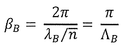
[0045]波長の光の場合: [0045] For light of wavelength:

[0046]回折格子と同一位相の光の場合、指数n1とn2の差は比較的小さい。ブラッグ波長では、透過損失は非常に少ない可能性がある;この波長における反射能は99.99%を超える可能性がある。 [0046] For light in phase with the grating, the difference between indices n1 and n2 is relatively small. At the Bragg wavelength, transmission losses can be very low; reflectivity at this wavelength can exceed 99.99%.
[0047]光起電デバイスへの光または光起電デバイス内の光を処理するための他のより従来型の提案されている解決法は、入射光を捕捉するか、さもなければ含有するためにブラッグ反射率を用いるが、波長シフトを提供する能力に欠ける。本開示の態様は、分布ブラッグ反射体構造の形成に量子マッチングを使用して波長シフティングの問題に対処する。量子閉じ込めブラッグ回折格子において、反射体配列は、光学利得を2倍増強するために、光エネルギーを波腹で維持する。 [0047] Other more conventional proposed solutions for processing light to or within photovoltaic devices capture or otherwise contain the incident light. uses Bragg reflectance for , but lacks the ability to provide wavelength shift. Aspects of the present disclosure address the problem of wavelength shifting using quantum matching in the formation of distributed Bragg reflector structures. In a quantum confined Bragg grating, a reflector array keeps the optical energy at the antinodes to enhance the optical gain by a factor of two.
[0048]態様に従って、量子閉じ込めまたは量子マッチングは、酸化ケイ素(SiO2)基材内に埋め込まれたシリコン(Si)ナノ粒子/ナノ結晶の分布を用いて達成される。分布しているナノ粒子間の空間は、SiO2基材内に垂直キャビティを形成する(“垂直”は、層およびPVデバイス表面の平面に対し概して直角方向に伸長している)。キャビティ内の光信号の共鳴は、全体的分布およびこれらのキャビティの垂直距離に対応する周波数(波長)で光コヒーレンスをもたらす。したがって、量子マッチングにおいて、DBR構造の1以上の各層内のナノ粒子の相対的濃度および分布は、Si/SiO2層の屈折率および得られるスペクトルシフティングの範囲の両方に影響を有する。 [0048] According to embodiments, quantum confinement or quantum matching is achieved using a distribution of silicon (Si) nanoparticles/nanocrystals embedded within a silicon oxide (SiO2) substrate. The spaces between the distributed nanoparticles form vertical cavities within the SiO2 substrate ("vertical" extends generally perpendicular to the plane of the layers and the PV device surface). Resonance of the optical signal within the cavities results in optical coherence at frequencies (wavelengths) corresponding to the global distribution and vertical distance of these cavities. Therefore, in quantum matching, the relative concentration and distribution of nanoparticles within each layer or layers of the DBR structure has an impact on both the refractive index of the Si/SiO2 layers and the extent of spectral shifting obtained.
[0049]本開示の態様によると、2つの異なる層が、DBRコーティング40構造中で交互になっている:
(i)図5に示す層状配列中の層60は、SiO2基材内にSi粒子の分布を有する工学的に設計された材料から形成され;
(ii)交互になっている層66は、インジウム-スズ酸化物(ITO)など他の透明な導電性材料から形成される。同様に用いることができる代替材料としては、さまざまなタイプのドープされた二元化合物、例えば、アルミニウムドープ酸化亜鉛(AZO)、インジウムドープ酸化カドミウム、およびアルミニウム、カリウムまたはインジウムがドープされた酸化亜鉛(AZO、GZOまたはIZO)などが挙げられる。
[0049] According to aspects of the present disclosure, two different layers alternate in the
(i)
(ii) alternating
[0050]基材およびナノ粒子構成要素を提供するために用いられる材料は、標的波長に適した幾何学的形状の垂直キャビティを形成するための適合性に関連して選択される。
SERS層46の構造および組成
[0051]ふたたび図4の略図を参照すると、SERS層46は、ブラッグ反射体部分44を通過する光の伝達および波長の初期シフティングに続いて、入ってくる光に追加的な波長シフトをもたらす波長変換機関を形成する。
[0050] The materials used to provide the substrate and nanoparticle components are selected for their suitability for forming a vertical cavity of geometry suitable for the target wavelength.
Structure and Composition of
[0051] Referring again to the schematic diagram of FIG. 4, the
[0052]光子のダウンコンバージョンを散乱およびストークスシフトで考えると、近共鳴ラマン散乱は、紫外線(UV)または可視(VIS)励起源、例えば325nm励起源と仮定すると、赤外線(IR)エネルギー領域にT2(LO)ピークをもたらす。したがって、例えば、325nm源は、対象となる600nm~1050nmの領域内にピークを生じさせることができる。生じるT2(LO)ピークの強度は、6nm~30nmのZnSナノ粒子サイズに伴い上昇する。 [0052] Considering photon downconversion in terms of scattering and Stokes shift, near-resonant Raman scattering is T2 yields a (LO) peak. Thus, for example, a 325 nm source can produce a peak in the 600 nm to 1050 nm region of interest. The intensity of the resulting T2(LO) peak increases with ZnS nanoparticle sizes from 6 nm to 30 nm.
[0053]態様において、表面増強ラマン効果は、350nm~450nmの範囲にあるUVおよびVISを、ラマンシフト(ストークスシフト)の結果、600nm~1000nm領域にあるT2(LO)ピークに励起させる。このシフトは、量子閉じ込めと、表面プラズモンによって作り出される自由励起子発光エネルギーとによって生じるバンドギャップエネルギーの変化によってもたらされることができる。ZnS金属ナノ粒子はストロークシフトに必要なプラズモンエネルギーを提供し、したがって、対象領域で放出されるシフトした光子のエネルギー損失をもたらさない。 [0053] In embodiments, the surface-enhanced Raman effect excites UV and VIS in the 350 nm-450 nm range to a T2 (LO) peak in the 600 nm-1000 nm region as a result of a Raman shift (Stokes shift). This shift can be brought about by bandgap energy changes caused by quantum confinement and free exciton emission energies created by surface plasmons. The ZnS metal nanoparticles provide the plasmon energy required for the stroke shift, thus resulting in no energy loss for the shifted photons emitted in the region of interest.
[0054]ラマン散乱は、分子材料の電子からの双極子雲(dipole cloud)の形成の結果である。ラマン散乱信号のスペクトルシフティングおよび表面増強は、SERS層46を形成する基材内での適切な材料、例えば、銀、金および亜鉛などの導電性ナノ粒子の分布に起因する。材料およびそれらの分布を適切に選択することにより、SERS層46を局在表面プラズモン共鳴(LSPR)を示すように構成して、適した波長範囲の方へのスペクトルシフティングを提供することができる。本明細書中で用いられる“導電性”という用語は、比較的低い体積抵抗率を有することをさし、例えば、限定されるものではないが、典型的な導電性材料は、20℃で102オーム-m未満である体積抵抗率を有する。体積抵抗率は、材料が電流の流れに逆らう能力に関連する。
[0054] Raman scattering is the result of the formation of a dipole cloud from the electrons of a molecular material. The spectral shifting and surface enhancement of the Raman scattering signal is due to the distribution of conductive nanoparticles such as suitable materials such as silver, gold and zinc within the substrate forming the
[0055]埋め込まれたナノ結晶の分布がまばらな媒体を通過する光の伝搬は、均質媒体の有効屈折率を計算することにより概算することができ、以下のように計算する: [0055] The propagation of light through a medium with a sparse distribution of embedded nanocrystals can be approximated by calculating the effective refractive index of a homogeneous medium, calculated as follows:
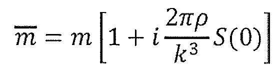
式中:
m=ナノ粒子が埋め込まれている光伝達性媒体の屈折率;
κ=ω/c 媒体中の波数;
ρ=N/V 粒子数N÷体積V;
S(0)は、前方向の散乱振幅である;
[0056]吸収媒体が複素屈折率を有する場合の吸収係数は、一般に以下である:
In the formula:
m = refractive index of the optically transmissive medium in which the nanoparticles are embedded;
κ=ω/c wavenumber in the medium;
ρ = N / V number of particles N / volume V;
S(0) is the forward scattering amplitude;
[0056] The absorption coefficient when the absorbing medium has a complex index of refraction is generally:

小さな同一ナノ粒子を含む薄層の場合、吸収係数は以下により与えることができる: For thin layers containing small identical nanoparticles, the absorption coefficient can be given by:

式中、Cextは単一粒子の消散断面積であり、散乱振幅ReS(0)の実部に比例する。
[0057]ベールの法則に従って、距離hにわたり有効媒体を通って伝搬する平行ビームの減衰は、以下を用いて得られる:
where C ext is the dissipation cross section of a single particle and is proportional to the real part of the scattering amplitude R e S(0).
[0057] According to Beer's law, the attenuation of a parallel beam propagating through an effective medium over a distance h is obtained using:
![]()
![]()
式中、Iは強度である。
[0058]波長シフティングは、本明細書中で参考として援用するvan Dijk et al.による“Competition between Extinction and Enhancement in Surface-Enhanced Raman Spectroscopy”という表題の論文、Physical Chemistry Letters, American Chemical Society, 2013. pp.1193-1196に記載されているように、競合過程の間の相互作用によって生じる。SERSは、ナノ粒子のプラズモン周波数において共鳴信号の消散をもたらすと同時に、共鳴波長からある距離において対応するラマン散乱信号の増強をもたらす働きをする。ナノ粒子がプラズモン共鳴で励起されたときにラマン信号が低減するこの直感に反した挙動は、典型的にPV適用に望ましい挙動である、より長波長への入射光のアップコンバージョンをもたらすように適合させることができる。あるいは、SERSは、波長バンドマッチングと同様に、より短波長への入射光のダウンコンバージョンを生じさせるために用いることができる。
where I is the intensity.
[0058] Wavelength shifting is described in van Dijk et al. in a paper entitled "Competition between Extinction and Enhancement in Surface-Enhanced Raman Spectroscopy", Physical Chemistry Letters, American Chemical Society, 2013. pp. 1193-1196, it arises through interactions between competing processes. SERS serves to provide resonance signal extinction at the nanoparticle's plasmon frequency while simultaneously providing corresponding enhancement of the Raman scattering signal at some distance from the resonance wavelength. This counterintuitive behavior of reduced Raman signal when nanoparticles are excited at plasmon resonance is adapted to result in upconversion of incident light to longer wavelengths, a behavior typically desired for PV applications. can be made Alternatively, SERS can be used to produce down-conversion of incident light to shorter wavelengths, similar to wavelength band matching.
[0059]ラマン散乱光エネルギーの波長および強度を調整するために制御することができる因子には、ナノ粒子のタイプ、形状、全体的サイズ、および濃度/分布がある。SERS構造を用いたスペクトル応答の設計は、例えば、A. Bouali, S. Haxha, F. Abdelmalek, M. Dridi,およびH. Bouchrihaによる“Tuning of Plasmonic Nanoparticle and Surface Enhanced Wavelength Shifting of a Nanosystem Sensing Using 3-D-FDTD Method”という表題の論文、IEEE Journal of Quantum Electronics Vol.50, No.8(2014年8月), pp.651-657に記載されており、これを本明細書中で参考として援用する。 [0059] Factors that can be controlled to tune the wavelength and intensity of the Raman scattered light energy include nanoparticle type, shape, overall size, and concentration/distribution. Spectral response design using SERS structures is described, for example, in A. et al. Bouali, S.; Haxha, F.; Abdelmalek, M.; Dridi, and H. Bouchriha, entitled "Tuning of Plasmonic Nanoparticles and Surface Enhanced Wavelength Shifting of a Nanosystem Sensing Using 3-D-FDTD Method," IEEE Quantum Journal of Economics Q. 50, No. 8 (August 2014), pp. 651-657, which is incorporated herein by reference.
[0060]プラズモン共鳴材料は、材料の粒径、サイズ、および周囲基材の誘電特性に特徴的な周波数スペクトルにわたり入射光を散乱させる。いくつかの材料についての共鳴散乱光は波長を増大させて、例えば入射光への“赤方偏移(red-shift)”をもたらすことができる。 [0060] Plasmon resonant materials scatter incident light over a frequency spectrum that is characteristic of the material's grain size, size, and the dielectric properties of the surrounding substrate. Resonantly scattered light for some materials can increase in wavelength, resulting in, for example, a "red-shift" to the incident light.
[0061]金属粒子におけるプラズモン発生の特徴は、その表面付近の領域における増強された電場の生成である。この電場と隣接材料の間の相互作用は、共鳴粒子および隣接材料の両方の散乱特性を著しく変化させることができる。表面増強ラマン分光法(SERS)では、ラマン散乱が数桁増強されるように工学的に設計された粒子コーティングされたフィルムにおける局在プラズモン共鳴が活用される。この技術を使用すると、対象材料に由来するラマン散乱を観察することができる;プラズモンによって生成される局所電場を用いて、散乱の強度を増強することができる。 [0061] A feature of plasmon generation in metal particles is the creation of an enhanced electric field in the region near their surface. The interaction between this electric field and neighboring materials can significantly change the scattering properties of both the resonant particles and the neighboring materials. Surface-enhanced Raman spectroscopy (SERS) exploits localized plasmon resonances in particle-coated films engineered to enhance Raman scattering by several orders of magnitude. Using this technique, Raman scattering originating from the material of interest can be observed; local electric fields generated by plasmons can be used to enhance the intensity of the scattering.
[0062]本開示の態様に従って、SERS層46は、透明な導電性ベース材料またはマトリックス内に埋め込まれた、酸化亜鉛(ZnO)または他の透明な導電性金属から形成された金属ナノ粒子から形成される。本開示の態様に従って、ITOは導電性ベース材料である。必要とされる波長シフティングの量に応じて、いくつかのタイプの金属ナノ粒子を、SERS層46でプラズモン応答を得るために用いることができる。適した金属ナノ粒子としては、金および銀などの貴金属、ならびに、低反応性および高反射に好ましい特性を有する金属、例えば、コバルトおよびクロムなどを挙げることができる。硝酸亜鉛などのさまざまな化合物を代替的に用いることができる。量子エレクトロニクス分野の技術者なら知っているように、もたらされるスペクトルシフトの量は、例えば適切に設計されたコーティングを施用することにより、材料中に工学的に設計することができる。達成されるスペクトルシフトは、部分的に、ナノ粒子のサイズおよび分布、ならびにベース材料またはマトリックスの複素屈折率の因子であることができる。
[0062] According to aspects of the present disclosure, the
[0063]さまざまなタイプのナノ粒子の使用、ならびに本開示のフィルムまたはコーティングの異なる層内でのそれらの相対的サイズおよび分布の制御により、アップコンバージョン、ダウンコンバージョン、または波長バンドマッチングへの使用を可能にする光波長の調整が可能になることに、留意すべきである。
ダウンコンバージョンフィルムの製作
[0064]例えば、太陽エネルギー変換適用に関し、出願人は、ダウンコンバージョンコーティングまたはフィルム40を上記配列を用いて形成すると、入射太陽光をPVデバイスによる効率的変換により好ましい波長に状態調整する適切な波長シフティングを提供することができることを見いだした。
[0063] The use of different types of nanoparticles and the control of their relative size and distribution within different layers of the films or coatings of the present disclosure allows for use in upconversion, downconversion, or wavelength band matching. It should be noted that the enabling light wavelength can be adjusted.
Production of down-conversion film
[0064] For example, with respect to solar energy conversion applications, Applicants have found that forming a down-conversion coating or
[0065]図4~6に示す層状配列に関し、製作工程は、透明なガラスまたはプラスチック基材であることができるカバー42から開始し、つぎにカバー42上にブラッグ反射体部分44の層を形成した後、SERS層46を形成する。
[0065] For the layered arrangement shown in FIGS. 4-6, the fabrication process begins with
[0066]ベースとしてのカバー42上にコーティング40を形成する工程は、以下の順序を用いることができる:
[0067](i)スパッタリングまたは他の付着技術を用いて50nmのITOまたは他の導電性光伝達性材料を付着させて、第1の層66を形成する。
[0066] The process of forming
[0067] (i)
[0068](ii)層66上にSiの薄層をスパッタリングするか、または他の方法で付着させる。
[0069](iii)焼結またはアニーリングを用いて付着Si層からナノ結晶を形成させる。態様によると、摂氏600~800度の範囲の焼結温度では、ITO層とは異なる所定の屈折率を有する層60を形成し、適した波長におけるブラッグ反射のための垂直キャビティを形成するのに望ましいナノ結晶分布を有するのに適したサイズおよび分布のSiナノ結晶が形成する。
(ii) Sputter or otherwise deposit a thin layer of Si on
[0069] (iii) Form nanocrystals from the deposited Si layer using sintering or annealing. According to embodiments, a sintering temperature in the range of 600 to 800 degrees Celsius is sufficient to form a
[0070](iv)形成したナノ結晶上にITOまたは他の導電性光伝達性材料を付着させることにより、埋め込み層を形成する。
[0071](v)工程(i)~(iv)を2回以上繰り返して、ブラッグ反射体部分44を形成する。
[0070] (iv) Forming a buried layer by depositing ITO or other conductive light transmissive material over the formed nanocrystals.
(v) Steps (i)-(iv) are repeated two or more times to form
[0072](vi)ITOなどの導電性透明ベースを適用し、該ベース上にZnOを埋め込むか、または他の方法で分布させることにより、SERS層を形成する。
[0073](vii)SERSを生じさせるのに適した分布を有するナノ粒子状ZnO粒子を形成する。
[0072] (vi) Applying a conductive transparent base such as ITO and embedding or otherwise distributing ZnO on the base to form the SERS layer.
[0073] (vii) forming nanoparticulate ZnO particles with a distribution suitable for producing SERS.
[0074]いくつかのナノ光学コーティングの形成方法が公知である。これらの方法としては、限定されるものではないが、ロールコーティング、スピンコーティング、物理蒸着、化学蒸着およびマグネトロンプラズマスパッタリングが挙げられる。ロールコーティングには、ポリマーバインダーから形成される充填剤および太陽光に暴露されると分解する充填剤を使用するという不利な点がある。 [0074] Several methods of forming nano-optical coatings are known. These methods include, but are not limited to, roll coating, spin coating, physical vapor deposition, chemical vapor deposition and magnetron plasma sputtering. Roll coating has the disadvantage of using fillers formed from polymeric binders and fillers that decompose on exposure to sunlight.
[0075]マグネトロンプラズマスパッタリングは、無機で持続時間の長い(long-lasting)金属酸化物、例えば、TiO2、SiO2、MgF2などのナノ光学コーティングに用いられる。この技術によりインライン処理が可能になり、好ましいサイクル時間内に非常に多くのガラスシートをスパッタリングすることができる。マグネトロンプラズマスパッタリング技術は、アディティブファブリケーション(additive fabrication)プロセスとしてナノ光学コーティングを一層ずつ構築する。 [0075] Magnetron plasma sputtering is used for nano-optical coatings of inorganic, long-lasting metal oxides, such as TiO2, SiO2, MgF2. This technique allows in-line processing, allowing a large number of glass sheets to be sputtered within a favorable cycle time. Magnetron plasma sputtering technology builds up nano-optical coatings layer by layer as an additive fabrication process.
[0076]図6の略図は、アディティブファブリケーションおよびその場でのコーティング内でのナノ粒子形成の順序を示す。左から右に、スパッタリングを用いて、(試料位置において)基材に材料および関連酸化物を施用する。その後、N2/O2雰囲気中のような制御条件下でのアニーリングプロセスを用いて、その基材へのコーティングを状態調整する。アニーリング温度は、限定されるものではないが、典型的には摂氏900~1200度の範囲にある。得られたナノ粒子を試験し、望ましい透過特性および反射特性をもたらすために用いることができる。 [0076] The schematic in Figure 6 shows the sequence of additive fabrication and nanoparticle formation within the in-situ coating. From left to right, sputtering is used to apply materials and related oxides to the substrate (at the sample location). An annealing process under controlled conditions, such as in a N2 / O2 atmosphere, is then used to condition the coating on the substrate. Annealing temperatures are typically, but not limited to, in the range of 900-1200 degrees Celsius. The resulting nanoparticles can be tested and used to provide desired transmission and reflection properties.
[0077]単一接合型c-Si太陽電池の上面および底面における良好な接触のために、透明導電性酸化物(TCO)内など、透明材料のマトリックスにナノ粒子を包含させるために、熱的アニーリングを達成することができる。同様に付加製造(additive manufacturing)プロセスを用いて金属酸化物のスパッタ層を熱的アニールしてその場でナノ結晶を作り出すことにより、改善された制御が可能になる;材料分野の技術者によく知られた方法を用いてアニーリングの温度および圧力を加えることにより、ナノ結晶活性層のサイズおよび密度の精密な制御が可能になる。 [0077] To incorporate the nanoparticles into a matrix of transparent material, such as in a transparent conductive oxide (TCO), for good contact on the top and bottom surfaces of single junction c-Si solar cells, thermal Annealing can be achieved. Similarly, using additive manufacturing processes to thermally anneal sputtered layers of metal oxides to create nanocrystals in situ allows for improved control; Applying the annealing temperature and pressure using known methods allows for precise control of the size and density of the nanocrystalline active layer.
[0078]記載した付加製造の順序は、インラインでの高処理量の処理に適している。石英ヒーターをスパッタリングチャンバー内に組み込むことができる。
[0079]態様によれば、700~1100nmのバンドパスと、PVおよび他の適用により適した、波長300nm~600nmの高エネルギー光子から800nm~900nmのより低エネルギーの光子へのダウンシフティング率が低いこととを達成するために、金属酸化物中で適切に構造化されて埋め込まれたナノ粒子を組み合わせる一連の工程がある。実験的コーティングの透過率および反射率スペクトルは、独立した試験によってバリデートされている。例えば、屋外試験では、72セルの実物大太陽電池パネルについて効率の向上が示され、野外実験に基づく太陽電池パネルの効率で平均15%~22%の全体的改善がみられる。
[0078] The additive manufacturing sequence described is suitable for in-line, high-throughput processing. A quartz heater can be incorporated into the sputtering chamber.
[0079] According to embodiments, the 700-1100 nm bandpass and the rate of downshifting from high energy photons at wavelengths 300 nm-600 nm to lower energy photons at 800 nm-900 nm, more suitable for PV and other applications There are a series of steps to combine appropriately structured embedded nanoparticles in metal oxides to achieve low . The transmittance and reflectance spectra of experimental coatings have been validated by independent testing. For example, field tests show improved efficiency for a 72-cell full-scale solar panel, with an average overall improvement of 15% to 22% in efficiency for solar panels based on field experiments.
[0080]図7の横断面の分解図は、本開示の態様に従って形成された透明なダウンコンバージョン(DC)フィルムまたはコーティング40に用いられる層状配列を、正確ではない縮尺で示している。フィルムまたはコーティング40は、ロール形態またはシート形態で製作した後、PVデバイス表面または他の基材の表面または構成要素に、例えばEVA(エチレン-酢酸ビニル)のような光学的接着剤を用いて施用することができる。
[0080] The cross-sectional exploded view of FIG. 7 illustrates, not to scale, the layered arrangement used in a transparent down-conversion (DC) film or
[0081]本開示の態様に従って、基材は、低鉄分の太陽電池用ガラス、例えば、インド、GujaratのGujarat Borosil Ltd.によって製造された太陽電池用ガラスであることができる。 [0081] According to aspects of the present disclosure, the substrate is a low iron solar glass, such as Gujarat Borosil Ltd., Gujarat, India. It can be a solar cell glass manufactured by
[0082]層は、いくつかの適した方法のいずれか、例えば、物理蒸着または化学蒸着により、光伝搬性基材上に形成することができる。焼結およびアニーリングプロセスは、例えば、高真空下または無酸素環境で実行することができる。 [0082] The layer can be formed on the light-transmissive substrate by any of several suitable methods, such as physical vapor deposition or chemical vapor deposition. Sintering and annealing processes can be performed, for example, under high vacuum or in an oxygen-free environment.
[0083]図7のフィルム40は、独立した光学的物品として用いることができ、または波長変換をもたらすために他の光学材料に付着させるか、または他の方法で連結することができる。
[0083] The
[0084]本開示の別の態様に従って、図7に示し本明細書中に記載するフィルム40は、ガラスまたは他の光学的材料または構成要素に施用するためのフィルム基材上に形成することができる。あるいは、フィルム40を形成する層は、改善されたスペクトル効率または応答のために、光伝搬性基材またはフォトニック構成要素の表面上に直接形成することができる。
[0084] In accordance with another aspect of the present disclosure, the
[0085]態様ではダウンコンバージョン機能について記載したが、本開示の装置および方法は、材料のタイプ、分布およびサイズを適切に変化させて、アップコンバージョンならびに好ましい波長範囲への光エネルギーのシフティングに代替的に適用することができる。 [0085] Although the embodiments describe a downconversion function, the apparatus and methods of the present disclosure can alternatively upconvert and shift light energy to a preferred wavelength range by appropriately changing the material type, distribution and size. can be applied
[0086]本開示の態様に従って、光学コーティングは、あらかじめ決定された波長範囲を反射するように形成された層のセットを有し、該層のセットは、交互になっている第1および第2の層を2対以上包含し、該第1の層は第1の屈折率n1を有し、該第2の層は、第1の屈折率n1より大きい第2の屈折率n2を有し、該第2の層はそれぞれ、第1の材料のナノ粒子の第1の分布を包含し、該層は、典型的には波長に対し光量または光エネルギーをプロットしたグラフによって示される、入射光波長の一部を第1の波長範囲にシフトさせ、第1の波長範囲の光を表面増強ラマン散乱層に方向付けるスペクトル特性を示す。表面増強ラマン散乱層は、第2の材料の導電性ナノ粒子の第2の分布により、第1の波長範囲の光が、ラマン散乱層中のナノ粒子の第2の分布に従って、第1の範囲とは異なる第2の波長範囲にさらにシフトするように構成される。層のスペクトル特性は、ナノ粒子の第1の分布内に形成される反射キャビティによって提供されることができる。第1の材料はシリコンであることができ;第2の材料は導電性金属であることができる。コーティングは、フィルムとして形成することができる。 [0086] According to an aspect of the present disclosure, the optical coating has a set of layers formed to reflect a predetermined wavelength range, the set of layers alternating first and second wherein the first layer has a first refractive index n1 and the second layer has a second refractive index n2 greater than the first refractive index n1 each of said second layers containing a first distribution of nanoparticles of a first material, said layers typically represented by a graph plotting light dose or light energy against wavelength; FIG. 1 shows spectral characteristics that shift a portion of incident light wavelengths to a first wavelength range and direct light in the first wavelength range to a surface-enhanced Raman scattering layer. The surface-enhanced Raman scattering layer is such that a second distribution of conductive nanoparticles of a second material causes light in a first wavelength range to scatter light in a first range according to a second distribution of nanoparticles in the Raman scattering layer. is configured to further shift to a second wavelength range different from. The spectral properties of the layer can be provided by reflective cavities formed within the first distribution of nanoparticles. The first material can be silicon; the second material can be a conductive metal. The coating can be formed as a film.
[0087]本開示の態様に従った光学コーティングは、標的波長を反射するように構成された分布ブラッグ反射体部分;ならびに、DBR部分に隣接し、DBR部分から標的波長の光を受け入れ、受け取った光からスペクトル的にシフトしている光を生じさせるように構成された、表面増強ラマン散乱部分;を有することができる。 [0087] An optical coating according to aspects of the present disclosure includes a distributed Bragg reflector portion configured to reflect a target wavelength; a surface-enhanced Raman scattering moiety configured to produce light that is spectrally shifted from the light.
[0088]本発明を詳細に記載し、適切または現在好ましい態様に特に関連して記載した可能性があるが、本発明の精神および範囲内で変動および改変をもたらすことができることは、理解されるであろう。したがって、ここで開示する態様は、あらゆる点で例示的であり、制約的ではないとみなされる。本発明の範囲は、添付する特許請求の範囲によって示され、その等価物の意味および範囲内で生じる変化はすべて、その中に包含されることを意図する。 [0088] While the invention has been described in detail and may have been described with particular reference to suitable or presently preferred embodiments, it is to be understood that variations and modifications can be effected within the spirit and scope of the invention. Will. Accordingly, the aspects disclosed herein are to be considered in all respects illustrative and not restrictive. The scope of the invention is indicated by the appended claims and all changes that come within the meaning and range of equivalents thereof are intended to be embraced therein.
20 PV変換器
40 コーティング
42 カバー
44 改変された分布ブラッグ反射体(DBR)部分
46 表面増強ラマン散乱(SERS)層
50 PV材料または他の基材
60 多層
66 多層
20
Claims (19)
あらかじめ決定された波長範囲を反射するように形成された層のセット、該層のセットは、交互になっている第1および第2の層を2対以上包含し、該第1の層は第1の屈折率n1を有し、該第2の層は、第1の屈折率n1より大きい第2の屈折率n2を有し、
該第2の層はそれぞれ、第1の材料のナノ粒子の第1の分布を包含し、
該層のセットは、入射光波長の一部を第1の波長範囲にシフトさせ、第1の波長範囲の光を表面増強ラマン散乱層に伝達する、スペクトル特性を示し;
該表面増強ラマン散乱層は、第2の材料のナノ粒子の第2の分布により、第1の波長範囲の光が、ラマン散乱層中のナノ粒子の第2の分布に従って、第1の範囲とは異なる第2の波長範囲にさらにシフトするように構成されている。 Optical coatings including:
A set of layers formed to reflect a predetermined range of wavelengths, the set of layers comprising two or more pairs of alternating first and second layers, the first layers having a refractive index n1 of 1 , the second layer having a second refractive index n2 greater than the first refractive index n1;
each of the second layers includes a first distribution of nanoparticles of a first material;
the set of layers exhibits spectral properties that shift a portion of incident light wavelengths to a first wavelength range and transmit light in the first wavelength range to the surface-enhanced Raman scattering layer;
The surface-enhanced Raman scattering layer is configured such that a second distribution of nanoparticles of a second material causes light in a first wavelength range to pass through the first range and a second distribution of nanoparticles in the Raman scattering layer. is configured to further shift to a different second wavelength range.
透過性材料から形成されたカバー層;
カバー層に隣接し、入射光範囲の光を受け取り、標的波長範囲の光を反射するように構成された、多層分布ブラッグ反射体部分;および
分布ブラッグ反射体部分に隣接し、分布ブラッグ反射体部分から標的波長範囲の光を受け入れ、受け取った光からスペクトル的にシフトしている出力光を生じさせるように構成された、表面増強ラマン散乱部分。 Optical coatings including:
a cover layer formed from a permeable material;
a multi-layer distributed Bragg reflector portion adjacent to the cover layer and configured to receive light in the incident light range and reflect light in the target wavelength range; and a distributed Bragg reflector portion adjacent to the distributed Bragg reflector portion. A surface-enhanced Raman scattering portion configured to accept light in a target wavelength range from and to produce output light that is spectrally shifted from the received light.
(a)層のセットを基材上に形成し、
該層のセットは、
(i)第1の屈折率n1を有する第1の層を付着させる工程、
(ii)第1の屈折率n1より大きい第2の屈折率n2を有する第2の層を付着させ、そして第1の材料のナノ粒子の第1の分布を有する第2の層を提供する工程、
を繰り返すことにより、入射光波長の一部を第1の波長範囲にシフトさせるスペクトル特性を示すように構成される、
(b)第2の材料のナノ粒子の第2の分布により、第1の波長範囲の光を受け取るように構成された表面増強ラマン散乱層を形成する、
該表面増強ラマン散乱層は、受け取った第1の波長範囲の光を、ラマン散乱層中のナノ粒子の第2の分布に従って、第1の範囲とは異なる第2の波長範囲にさらにシフトさせる。 Methods of forming optical coatings, including:
(a) forming a set of layers on a substrate;
The set of layers includes:
(i) depositing a first layer having a first refractive index n1;
(ii) depositing a second layer having a second refractive index n2 greater than the first refractive index n1 and providing the second layer having a first distribution of nanoparticles of the first material; the process of
configured to exhibit a spectral characteristic that shifts a portion of the incident light wavelengths to a first wavelength range by repeating
(b) a second distribution of nanoparticles of a second material to form a surface-enhanced Raman scattering layer configured to receive light in the first wavelength range;
The surface-enhanced Raman scattering layer further shifts received light in a first wavelength range to a second wavelength range different from the first range according to a second distribution of nanoparticles in the Raman scattering layer.
Applications Claiming Priority (3)
| Application Number | Priority Date | Filing Date | Title |
|---|---|---|---|
| US201962913315P | 2019-10-10 | 2019-10-10 | |
| US62/913,315 | 2019-10-10 | ||
| PCT/US2020/054586 WO2021071953A1 (en) | 2019-10-10 | 2020-10-07 | Optical coating for spectral conversion |
Publications (1)
| Publication Number | Publication Date |
|---|---|
| JP2022551920A true JP2022551920A (en) | 2022-12-14 |
Family
ID=73198434
Family Applications (1)
| Application Number | Title | Priority Date | Filing Date |
|---|---|---|---|
| JP2022521654A Pending JP2022551920A (en) | 2019-10-10 | 2020-10-07 | Optical coating for spectral conversion |
Country Status (9)
| Country | Link |
|---|---|
| US (1) | US10935707B1 (en) |
| EP (1) | EP4042490A1 (en) |
| JP (1) | JP2022551920A (en) |
| CN (1) | CN115039238B (en) |
| AU (1) | AU2020363647A1 (en) |
| BR (1) | BR112022006808A2 (en) |
| CA (1) | CA3157321A1 (en) |
| WO (1) | WO2021071953A1 (en) |
| ZA (1) | ZA202203512B (en) |
Families Citing this family (2)
| Publication number | Priority date | Publication date | Assignee | Title |
|---|---|---|---|---|
| US11851743B1 (en) * | 2022-08-19 | 2023-12-26 | SunDensity, Inc. | Metal nanoparticle fabrication on TCO for plasmonic interaction of photons |
| CN116014019A (en) * | 2023-01-10 | 2023-04-25 | 华为数字能源技术有限公司 | A kind of thin-film solar cell, its preparation method, photovoltaic module and power generation equipment |
Citations (2)
| Publication number | Priority date | Publication date | Assignee | Title |
|---|---|---|---|---|
| JP2013065833A (en) * | 2011-08-24 | 2013-04-11 | Commissariat A L'energie Atomique & Aux Energies Alternatives | Method of manufacturing optical reflector with semiconductor nanocrystals |
| JP2018121072A (en) * | 2012-10-11 | 2018-08-02 | ザ リージェンツ オブ ザ ユニヴァシティ オブ ミシガン | Organic photoelectric device with reflector |
Family Cites Families (18)
| Publication number | Priority date | Publication date | Assignee | Title |
|---|---|---|---|---|
| GB8602304D0 (en) | 1986-01-30 | 1986-03-05 | Dakubu S | Dihydropyridine condensation products |
| US20040142484A1 (en) * | 2002-09-30 | 2004-07-22 | Intel Corporation | Spectroscopic analysis system and method |
| DE102005000767A1 (en) * | 2005-01-04 | 2006-07-20 | Rwe Space Solar Power Gmbh | Monolithic multiple solar cell |
| US20070295383A1 (en) | 2006-03-31 | 2007-12-27 | Intematix Corporation | Wavelength-converting phosphors for enhancing the efficiency of a photovoltaic device |
| US8861072B2 (en) * | 2008-05-30 | 2014-10-14 | Opalux Incorporated | Tunable Bragg stack |
| DE102008029711A1 (en) * | 2008-06-24 | 2010-01-07 | Krones Ag | Changeable gripping element for transporting containers |
| US10105875B2 (en) * | 2008-08-21 | 2018-10-23 | Cam Holding Corporation | Enhanced surfaces, coatings, and related methods |
| US20100126567A1 (en) | 2008-11-21 | 2010-05-27 | Lightwave Power, Inc. | Surface plasmon energy conversion device |
| US20100126566A1 (en) | 2008-11-21 | 2010-05-27 | Lightwave Power, Inc. | Surface plasmon wavelength converter |
| US20100288352A1 (en) * | 2009-05-12 | 2010-11-18 | Lightwave Power, Inc. | Integrated solar cell nanoarray layers and light concentrating device |
| US10847666B2 (en) * | 2009-09-25 | 2020-11-24 | Immunolight, Llc | Up and down conversion systems for improved solar cell performance or other energy conversion |
| US20120037228A1 (en) | 2010-08-10 | 2012-02-16 | Du Pont Apollo Limited | Thin-Film Photovoltaic Cell Having Distributed Bragg Reflector |
| US20120080067A1 (en) * | 2010-09-30 | 2012-04-05 | General Electric Company | Photovoltaic devices |
| CN103904174B (en) * | 2014-04-11 | 2016-08-24 | 安徽三安光电有限公司 | The manufacture method of light-emitting diode chip for backlight unit |
| CN104678469B (en) * | 2015-03-17 | 2018-11-02 | 中国科学院上海高等研究院 | Graded index materials distributed bragg reflector mirror and its manufacturing method |
| US9954128B2 (en) | 2016-01-12 | 2018-04-24 | The Boeing Company | Structures for increased current generation and collection in solar cells with low absorptance and/or low diffusion length |
| CN109580586A (en) * | 2019-01-07 | 2019-04-05 | 重庆大学 | SF6Decompose gas joint enhancing Raman spectrum detecting device and detection method |
| CN117452544A (en) * | 2023-10-31 | 2024-01-26 | 苏州山河光电科技有限公司 | Linear polaroid based on super-surface optical structure |
-
2020
- 2020-10-07 CA CA3157321A patent/CA3157321A1/en active Pending
- 2020-10-07 AU AU2020363647A patent/AU2020363647A1/en not_active Abandoned
- 2020-10-07 BR BR112022006808A patent/BR112022006808A2/en unknown
- 2020-10-07 EP EP20804019.6A patent/EP4042490A1/en not_active Withdrawn
- 2020-10-07 US US17/064,699 patent/US10935707B1/en active Active
- 2020-10-07 JP JP2022521654A patent/JP2022551920A/en active Pending
- 2020-10-07 CN CN202080085766.8A patent/CN115039238B/en not_active Expired - Fee Related
- 2020-10-07 WO PCT/US2020/054586 patent/WO2021071953A1/en not_active Ceased
-
2022
- 2022-03-25 ZA ZA2022/03512A patent/ZA202203512B/en unknown
Patent Citations (2)
| Publication number | Priority date | Publication date | Assignee | Title |
|---|---|---|---|---|
| JP2013065833A (en) * | 2011-08-24 | 2013-04-11 | Commissariat A L'energie Atomique & Aux Energies Alternatives | Method of manufacturing optical reflector with semiconductor nanocrystals |
| JP2018121072A (en) * | 2012-10-11 | 2018-08-02 | ザ リージェンツ オブ ザ ユニヴァシティ オブ ミシガン | Organic photoelectric device with reflector |
Non-Patent Citations (1)
| Title |
|---|
| J.WALSHE ET AL: "BRAGG ENHANCED PLASMONIC LUMINESCENT DOWNSHIFTING FOR PV DEVICES", 32ND EUROPEAN PHOTOVOLTAIC SOLAR ENERGY CONFERENCE AND EXHIBITION, JPN6024016797, 29 June 2016 (2016-06-29), pages 1 - 5, ISSN: 0005557753 * |
Also Published As
| Publication number | Publication date |
|---|---|
| CN115039238B (en) | 2024-04-26 |
| CA3157321A1 (en) | 2021-04-15 |
| WO2021071953A1 (en) | 2021-04-15 |
| CN115039238A (en) | 2022-09-09 |
| BR112022006808A2 (en) | 2022-06-28 |
| US10935707B1 (en) | 2021-03-02 |
| EP4042490A1 (en) | 2022-08-17 |
| ZA202203512B (en) | 2024-10-30 |
| AU2020363647A1 (en) | 2022-04-21 |
Similar Documents
| Publication | Publication Date | Title |
|---|---|---|
| Ferry et al. | Plasmonic nanostructure design for efficient light coupling into solar cells | |
| Xu et al. | Enhanced photon collection in luminescent solar concentrators with distributed Bragg reflectors | |
| JP7526790B2 (en) | Method and apparatus for enhanced solar energy conversion - Patents.com | |
| Rehman et al. | Super absorption of solar energy using a plasmonic nanoparticle based CdTe solar cell | |
| JPWO2018043298A1 (en) | Light absorber, bolometer, infrared absorber, solar thermal power generator, radiation cooling film, and method of manufacturing light absorber | |
| CN116088077B (en) | A dual-wave dynamic thermal camouflage structure and its optimization method | |
| Bora et al. | Plasmonic black metals in resonant nanocavities | |
| Saravanan et al. | Study of ultrathin‐film amorphous silicon solar cell performance using photonic and plasmonic nanostructure | |
| JP2022551920A (en) | Optical coating for spectral conversion | |
| Yang et al. | Light trapping enhancement in a thin film with 2D conformal periodic hexagonal arrays | |
| CN112161954A (en) | Plasmon refractive index sensor based on out-of-plane lattice point resonance | |
| Jalali | Impact of one-dimensional photonic crystal back reflector in thin-film c-Si solar cells on efficiency: Impact of one-dimensional photonic crystal | |
| Wang et al. | Plasmonic light trapping in an ultrathin photovoltaic layer with film-coupled metamaterial structures | |
| Cui et al. | Electric and magnetic resonances in optical metamaterial for efficient absorption enhancement in ultrathin CdTe-based photovoltaic cells | |
| Jakšić et al. | Plasmonic enhancement of light trapping in photodetectors | |
| Ramachandran et al. | Antireflective coatings and optical filters | |
| Shabat et al. | Finite Difference Time Domain Simulation of light trapping in a GaAs complex structure | |
| Armghan et al. | Thin wire and circular disk resonator MXene solar absorber optimized using Machine learning for renewable energy applications | |
| Hyun Lee et al. | Light confinement-induced antireflection of ZnO nanocones | |
| CN118837982B (en) | Adjustable absorber | |
| Catchpole et al. | Novel applications for surface plasmons in photovoltaics | |
| Marrocco et al. | Modification of the scattering of silver nanoparticles induced by Fabry–Perot resonances rising from a finite Si layer | |
| Gad et al. | Enhancing the performance of thin film photovoltaic solar cells using truncated conical nanoparticles | |
| Dubey et al. | Light trapping enhancement in thin film silicon solar cell with different back reflector | |
| Jagathpriya et al. | Effect of Mirror Characteristics on Critical Coupling in Plasmonic Nanostructures |
Legal Events
| Date | Code | Title | Description |
|---|---|---|---|
| A621 | Written request for application examination |
Free format text: JAPANESE INTERMEDIATE CODE: A621 Effective date: 20230418 |
|
| A977 | Report on retrieval |
Free format text: JAPANESE INTERMEDIATE CODE: A971007 Effective date: 20240312 |
|
| A131 | Notification of reasons for refusal |
Free format text: JAPANESE INTERMEDIATE CODE: A131 Effective date: 20240501 |
|
| A521 | Request for written amendment filed |
Free format text: JAPANESE INTERMEDIATE CODE: A523 Effective date: 20240625 |
|
| A131 | Notification of reasons for refusal |
Free format text: JAPANESE INTERMEDIATE CODE: A131 Effective date: 20241002 |
|
| A02 | Decision of refusal |
Free format text: JAPANESE INTERMEDIATE CODE: A02 Effective date: 20250325 |