JP2022143679A - Photoelectric conversion elements, electronic devices, and power supply modules - Google Patents
Photoelectric conversion elements, electronic devices, and power supply modules Download PDFInfo
- Publication number
- JP2022143679A JP2022143679A JP2021044329A JP2021044329A JP2022143679A JP 2022143679 A JP2022143679 A JP 2022143679A JP 2021044329 A JP2021044329 A JP 2021044329A JP 2021044329 A JP2021044329 A JP 2021044329A JP 2022143679 A JP2022143679 A JP 2022143679A
- Authority
- JP
- Japan
- Prior art keywords
- photoelectric conversion
- electrode
- conversion element
- layer
- transport layer
- Prior art date
- Legal status (The legal status is an assumption and is not a legal conclusion. Google has not performed a legal analysis and makes no representation as to the accuracy of the status listed.)
- Pending
Links
Images


Classifications
-
- H—ELECTRICITY
- H10—SEMICONDUCTOR DEVICES; ELECTRIC SOLID-STATE DEVICES NOT OTHERWISE PROVIDED FOR
- H10K—ORGANIC ELECTRIC SOLID-STATE DEVICES
- H10K30/00—Organic devices sensitive to infrared radiation, light, electromagnetic radiation of shorter wavelength or corpuscular radiation
- H10K30/80—Constructional details
- H10K30/88—Passivation; Containers; Encapsulations
-
- H—ELECTRICITY
- H10—SEMICONDUCTOR DEVICES; ELECTRIC SOLID-STATE DEVICES NOT OTHERWISE PROVIDED FOR
- H10K—ORGANIC ELECTRIC SOLID-STATE DEVICES
- H10K85/00—Organic materials used in the body or electrodes of devices covered by this subclass
- H10K85/10—Organic polymers or oligomers
- H10K85/111—Organic polymers or oligomers comprising aromatic, heteroaromatic, or aryl chains, e.g. polyaniline, polyphenylene or polyphenylene vinylene
- H10K85/113—Heteroaromatic compounds comprising sulfur or selene, e.g. polythiophene
Landscapes
- Physics & Mathematics (AREA)
- Electromagnetism (AREA)
- Photovoltaic Devices (AREA)
- Electroluminescent Light Sources (AREA)
Abstract
【課題】高温高湿環境下に長時間置かれても光電変換効率が低下しない光電変換素子を提供する。【解決手段】第一の電極13、光電変換層、及び第二の電極を順次有する光電変換素子であって、第二の電極と光電変換層とを内包し、且つ第一の電極13における接着領域と接着する封止部材を有し、封止部材は接着部材21を含んでおり、光電変換素子の積層方向を含む断面において、第一の電極13における接着領域を有さない面から前記接着領域と接着している接着部材21までの積層方向における長さの最大値Lmax及び最小値Lminの差は、1000nm以下であることを特徴とする光電変換素子。【選択図】図3Kind Code: A1 A photoelectric conversion element is provided in which the photoelectric conversion efficiency does not decrease even when placed in a high-temperature and high-humidity environment for a long time. A photoelectric conversion element having a first electrode (13), a photoelectric conversion layer, and a second electrode in this order, the second electrode and the photoelectric conversion layer are included, and adhesion in the first electrode (13) is provided. It has a sealing member that adheres to the region, the sealing member includes an adhesive member 21, and in a cross section including the stacking direction of the photoelectric conversion element, the bonding is performed from the surface of the first electrode 13 that does not have a bonding region. A photoelectric conversion element, wherein the difference between the maximum value Lmax and the minimum value Lmin of the length in the stacking direction up to the adhesive member 21 bonded to the region is 1000 nm or less. [Selection drawing] Fig. 3
Description
本発明は、光電変換素子、電子機器、及び電源モジュールに関する。 The present invention relates to photoelectric conversion elements, electronic devices, and power supply modules.
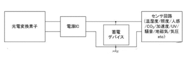
近年、あらゆるものがインターネットに接続し、包括的な制御を可能とするIoT(Internet of Things)社会の実現が期待されている。このようなIoT社会の実現のためには、多数のセンサを様々なものに取り付け、データを取得することが求められているが、多数のセンサを動かす電源が必要となる。多数のセンサへの配線や蓄電池の使用は実用的ではなく、また、環境負荷低減への社会的なニーズの高まりから、環境発電素子による給電が期待されている。 In recent years, there are expectations for the realization of an IoT (Internet of Things) society in which everything is connected to the Internet and comprehensive control is possible. In order to realize such an IoT society, it is required to attach a large number of sensors to various things and acquire data. Wiring to a large number of sensors and the use of storage batteries are not practical, and power supply by energy harvesting elements is expected due to the increasing social needs for reducing environmental load.
これらの中でも、光電変換素子は光があればどこでも発電できる素子として注目を集めている。特にフレキシブル性を持った光電変換素子は、高効率であることが期待されるとともに、様々な曲面に追従可能であってウェアラブルデバイス等へ適応可能であることも併せて期待されている。
例えば、非特許文献1及び2には、光電変換素子のウェアラブルデバイスに対する可能性検討の結果が報告されている。
また、一般的にフレキシブル性を有する高効率な環境発電素子としては、有機薄膜太陽電池が期待されており、特許文献1では、透明基材フィルムを基材とする光電変換素子が提案されている。
Among these, photoelectric conversion elements are attracting attention as elements that can generate electricity anywhere as long as there is light. In particular, flexible photoelectric conversion elements are expected to have high efficiency, and are also expected to be able to follow various curved surfaces and to be applicable to wearable devices and the like.
For example, Non-Patent
In addition, organic thin-film solar cells are generally expected as highly efficient energy harvesting elements having flexibility, and
一般的な有機薄膜太陽電池における光電変換素子は、支持基板である基材上に、第一の電極、電子輸送層、光電変換層、正孔輸送層、及び第二の電極をこの順で積層した構造を有する。一方で、このような構造を有する光電変換素子は、内部に水等が侵入することで機能が低下するため、外部物質が光電変換素子内部へ侵入することを抑制する封止部材が更に設けられている。このような封止部材としては、例えば、上記構造を有する光電変換素子において、第二の電極側からフィルムを被せて基材側の部材と貼り合わせる部材等が知られている。 A photoelectric conversion element in a general organic thin-film solar cell is formed by stacking a first electrode, an electron transport layer, a photoelectric conversion layer, a hole transport layer, and a second electrode in this order on a substrate, which is a support substrate. It has a structure that On the other hand, since the function of the photoelectric conversion element having such a structure deteriorates due to intrusion of water or the like into the interior, a sealing member is further provided to suppress the intrusion of external substances into the photoelectric conversion element. ing. As such a sealing member, for example, in the photoelectric conversion element having the structure described above, a member that is covered with a film from the second electrode side and bonded to the member on the substrate side is known.
しかしながら、外部物質の侵入を抑制する封止部材を有する光電変換素子であっても、高温高湿環境下に長時間置かれることで光電変換効率が低下する課題がある。 However, even a photoelectric conversion element having a sealing member that suppresses intrusion of external substances has a problem that the photoelectric conversion efficiency is lowered by being placed in a high-temperature and high-humidity environment for a long time.
本発明は、第一の電極、光電変換層、及び第二の電極を順次有する光電変換素子であって、前記第一の電極及び前記第二の電極から選ばれる一方の電極と光電変換層とを内包し、且つ前記第一の電極及び前記第二の電極から選ばれる他方の電極における接着領域と接着する封止部材を有し、前記光電変換素子の積層方向を含む断面において、前記他方の電極における前記接着領域を有さない面から前記接着領域と接着している前記封止部材までの積層方向における長さLの最大値及び最小値の差は、1000nm以下であることを特徴とする光電変換素子に関する。 The present invention is a photoelectric conversion element having a first electrode, a photoelectric conversion layer, and a second electrode in sequence, wherein one electrode selected from the first electrode and the second electrode and the photoelectric conversion layer and has a sealing member that adheres to an adhesion region in the other electrode selected from the first electrode and the second electrode, and in a cross section including the stacking direction of the photoelectric conversion element, the other A difference between a maximum value and a minimum value of a length L in the stacking direction from a surface of the electrode not having the bonding region to the sealing member bonded to the bonding region is 1000 nm or less. It relates to a photoelectric conversion element.
本発明によれば、高温高湿環境下に長時間置かれたとしても光電変換効率の低下が抑制される光電変換素子を提供することができる。 ADVANTAGE OF THE INVENTION According to this invention, the photoelectric conversion element which can suppress the fall of a photoelectric conversion efficiency even if it sets to a high-temperature and high-humidity environment for a long time can be provided.
以下、本発明の実施形態の一例について説明する。 An example of an embodiment of the present invention will be described below.
<<光電変換素子>>
「光電変換素子」とは、光エネルギーを電気エネルギーに変換する素子または電気エネルギーを光エネルギーに変換する素子である。具体的には、太陽電池およびフォトダイオードなどを構成する素子が挙げられる。
<<Photoelectric conversion element>>
A “photoelectric conversion device” is a device that converts light energy into electrical energy or a device that converts electrical energy into light energy. Specific examples include elements that constitute solar cells, photodiodes, and the like.
光電変換素子は、少なくとも、第一の電極、光電変換層、及び第二の電極を順次有する。「順次」とは、これら電極および層が全体として上記の順で並んでいればよく、電極と層との間に他の層などが挿入されていてもよい。他の層が挿入されている場合としては、例えば、第一の電極、電子輸送層、光電変換層、正孔輸送層、及び第二の電極を順次有する光電変換素子が挙げられる。この場合、更に、電極と層との間または層と層との間に他の層などが挿入されていてもよい。また、「順次」とは、これら電極および層が、第一の電極側から順に積層されていてもよいし、第二の電極側から順に積層されていてもよいことを表す。具体的には、光電変換素子は、光の入射面側から観察した場合に、第一の電極、光電変換層、及び第二の電極の順に積層されていてもよいし、第二の電極、光電変換層、及び第一の電極の順に積層されていてもよい。また、光電変換素子が電子輸送層および正孔輸送層を有す場合、光電変換素子は、光の入射面側から観察した場合に、第一の電極、電子輸送層、光電変換層、正孔輸送層、及び第二の電極の順に積層されていてもよいし、第二の電極、正孔輸送層、光電変換層、電子輸送層、及び第一の電極の順に積層されていてもよい。なお、本開示では、光の入射面側から観察した場合に、第一の電極、電子輸送層、光電変換層、正孔輸送層、及び第二の電極の順に積層されている場合を主に説明するが、本光電変換素子はかかる態様に限定されない。当業者であれば、かかる説明から他の態様、すなわち、光の入射面側から観察した場合に、第二の電極、正孔輸送層、光電変換層、電子輸送層、及び第一の電極の順に積層されている場合などについても容易に理解できる。 A photoelectric conversion element has at least a first electrode, a photoelectric conversion layer, and a second electrode in this order. "Sequentially" means that these electrodes and layers are arranged in the above order as a whole, and other layers may be inserted between the electrodes and the layers. Examples of the case where other layers are inserted include a photoelectric conversion element having a first electrode, an electron transport layer, a photoelectric conversion layer, a hole transport layer, and a second electrode in this order. In this case, another layer or the like may be inserted between the electrode and the layer or between the layers. Further, "sequentially" means that these electrodes and layers may be laminated in order from the first electrode side, or may be laminated in order from the second electrode side. Specifically, the photoelectric conversion element may be laminated in order of the first electrode, the photoelectric conversion layer, and the second electrode when observed from the light incident surface side, or the second electrode, The photoelectric conversion layer and the first electrode may be laminated in this order. When the photoelectric conversion element has an electron-transporting layer and a hole-transporting layer, when viewed from the light incident surface side, the photoelectric conversion element includes the first electrode, the electron-transporting layer, the photoelectric conversion layer, the hole The transport layer and the second electrode may be stacked in this order, or the second electrode, the hole transport layer, the photoelectric conversion layer, the electron transport layer and the first electrode may be stacked in this order. In the present disclosure, when observed from the light incident surface side, the first electrode, the electron transport layer, the photoelectric conversion layer, the hole transport layer, and the second electrode are mainly laminated in this order. Although explained, the present photoelectric conversion element is not limited to such an aspect. A person skilled in the art will understand from such a description other aspects, that is, when observed from the light incident surface side, the second electrode, the hole transport layer, the photoelectric conversion layer, the electron transport layer, and the first electrode. It is easy to understand the case where the layers are laminated in order.
光電変換素子は、封止部材を有する。封止部材は、第一の電極及び第二の電極から選ばれる一方の電極(以下、「一方の電極」とも称する)と光電変換層とを内包し、光電変換素子が電子輸送層及び正孔輸送層を有する場合は、更に、電子輸送層及び正孔輸送層も内包する。また、封止部材は、第一の電極及び第二の電極から選ばれる他方の電極(以下、「他方の電極」とも称する)における接着領域と接着する。なお、「内包」とは、少なくとも封止部材及び他方の電極で形作られる空間内に一方の電極及び光電変換層などが設けられていることを表す。なお、上記空間は封止部材及び他方の電極に加えて他の構成(端子等)で形作られていてもよい。「接着領域」とは、他方の電極において封止部材と直接的又は間接的に接触することで接着される領域であって、一方の電極と対向する面の一部に位置する領域である。また、「一方の電極」及び「他方の電極」の位置関係は、特に限定されない。本開示では、一方の電極が光の入射面から遠い位置に設けられた電極であり、他方の電極が光の入射面から近い位置に設けられた電極である場合を主に説明するが、本光電変換素子はかかる態様に限定されない。当業者であれば、かかる説明から他の態様、すなわち、一方の電極が光の入射面から近い位置に設けられた電極であり、他方の電極が光の入射面から遠い位置に設けられた電極である場合などについても容易に理解できる。 A photoelectric conversion element has a sealing member. The sealing member includes one electrode selected from the first electrode and the second electrode (hereinafter also referred to as "one electrode") and the photoelectric conversion layer, and the photoelectric conversion element includes the electron transport layer and the hole When it has a transport layer, it also includes an electron transport layer and a hole transport layer. Also, the sealing member adheres to the adhesion region of the other electrode selected from the first electrode and the second electrode (hereinafter also referred to as "the other electrode"). Note that the term “inclusive” means that one electrode, a photoelectric conversion layer, and the like are provided in a space defined by at least the sealing member and the other electrode. In addition to the sealing member and the other electrode, the space may be formed by other structures (terminals, etc.). The “adhesion region” is a region where the other electrode is adhered by direct or indirect contact with the sealing member, and is a region located on a part of the surface facing the one electrode. In addition, the positional relationship between "one electrode" and "the other electrode" is not particularly limited. In the present disclosure, a case where one electrode is provided far from the light incident surface and the other electrode is provided close to the light incident surface will be mainly described. A photoelectric conversion element is not limited to this aspect. A person skilled in the art will understand from such a description other aspects, that is, an electrode in which one electrode is provided at a position close to the light incident surface and the other electrode is provided at a position far from the light incident surface. , etc., can be easily understood.
また、光電変換素子は、必要に応じて、基材、表面保護層、UVカット層などを有する。
基材を有する場合、光電変換素子は、光の入射面側から観察した場合に、基材、第一の電極、電子輸送層、光電変換層、正孔輸送層、及び第二の電極の順に積層されている構成、又は基材、第二の電極、正孔輸送層、光電変換層、電子輸送層、及び第一の電極の順に積層されている構成を有することが好ましい。また、基材は、他方の電極の接着領域を有さない面側において、他方の電極と隣接して設けられていることが好ましい。
Moreover, the photoelectric conversion element has a base material, a surface protective layer, a UV cut layer, etc., as required.
When the photoelectric conversion element has a substrate, when observed from the light incident surface side, the substrate, the first electrode, the electron transport layer, the photoelectric conversion layer, the hole transport layer, and the second electrode in that order. It is preferable to have a laminated structure or a structure in which the substrate, the second electrode, the hole transport layer, the photoelectric conversion layer, the electron transport layer, and the first electrode are laminated in this order. Moreover, it is preferable that the base material is provided adjacent to the other electrode on the side of the other electrode that does not have the bonding region.
<基材>
「基材」とは、光電変換素子を構成する各電極及び各層などを支持する部材である。基材は、光電変換効率を高める観点から光透過性が高いことが好ましく、透明であることがより好ましい。また、基材は、光電変換素子の用途の幅を広げる観点からフレキシブル性が高いことが好ましい。
<Base material>
A “base material” is a member that supports each electrode, each layer, and the like that constitute a photoelectric conversion element. From the viewpoint of increasing the photoelectric conversion efficiency, the substrate preferably has high light transmittance, and is more preferably transparent. Moreover, it is preferable that the base material has high flexibility from the viewpoint of widening the range of applications of the photoelectric conversion element.
透明性及びフレキシブル性を有する基材の材料としては、例えば、ポリエチレンテレフタレート等のポリエステル、ポリカーボネート、ポリイミド、ポリメチルメタクリレート、ポリスルホン、及びポリエーテルエーテルケトン等の樹脂フィルム、並びに平均厚みが200μm以下の薄膜ガラスなどが挙げられる。これら材料の中でも、易製造性及びコストの観点から、ポリエステル及びポリイミドの樹脂フィルム、並びに薄膜ガラスが好ましい。
透明性を有するがフレキシブル性を有さない基材の材料としては、例えば、ガラスなどの無機物透明結晶体などが挙げられる。これら材料は、フレキシブル性を有さないが高い平坦性を有するため好ましい。
なお、基材は、ガスバリア性を有することが好ましい。ガスバリア性とは、水蒸気や酸素などの透過を抑制する機能である。本開示において「ガスバリア性を有する基材」とは、基材自体がガスバリア性を有するものに限定されず、基材に隣接する位置にガスバリア性を有する層であるガスバリア層を有するものも含まれる。基材がガスバリア性を有することで、高温高湿環境下に長時間置かれたとしても光電変換効率の低下がより抑制される光電変換素子を提供することができる。なお、ガスバリア層については後述する。
ガスバリア性を有する基材に要求される機能は、一般的に水蒸気透過量及び酸素透過量などで表現される。JIS K7129 B法準拠に準拠する一日あたりの水蒸気透過量は、例えば、1×10⁻²g/m2以下であることが好ましく、低ければ低いほど好ましい。また、JIS K7126-2に準拠する一日あたりの酸素透過量は、例えば、1cm3/m2・atm以下であることが好ましく、低ければ低いほど好ましい。
なお、ガスバリア性を有する樹脂フィルムとしては、適宜公知のものを用いることができ、例えば、アルミニウム被覆された樹脂フィルムや酸化ケイ素被覆された樹脂フィルムなどが挙げられる。
Materials for the substrate having transparency and flexibility include resin films such as polyester such as polyethylene terephthalate, polycarbonate, polyimide, polymethylmethacrylate, polysulfone, and polyetheretherketone, and thin films having an average thickness of 200 μm or less. Glass etc. are mentioned. Among these materials, polyester and polyimide resin films and thin glass are preferred from the viewpoint of ease of manufacture and cost.
Examples of materials for the base material having transparency but not flexibility include inorganic transparent crystals such as glass. These materials are preferred because they do not have flexibility but have high flatness.
In addition, it is preferable that the base material has a gas barrier property. The gas barrier property is a function of suppressing permeation of water vapor, oxygen, and the like. In the present disclosure, the term "substrate having gas barrier properties" is not limited to those in which the substrate itself has gas barrier properties, but also includes substrates having a gas barrier layer, which is a layer having gas barrier properties, adjacent to the substrate. . Since the base material has gas barrier properties, it is possible to provide a photoelectric conversion element in which a decrease in photoelectric conversion efficiency is further suppressed even when placed in a high-temperature, high-humidity environment for a long time. Note that the gas barrier layer will be described later.
The functions required for a base material having gas barrier properties are generally expressed by the amount of water vapor permeation, the amount of oxygen permeation, and the like. The water vapor permeation amount per day conforming to JIS K7129 B method is preferably, for example, 1×10 −2 g/m 2 or less, and the lower the better. In addition, the oxygen permeation amount per day according to JIS K7126-2 is preferably, for example, 1 cm 3 /m 2 ·atm or less, and the lower the better.
As the resin film having gas barrier properties, a known one can be used as appropriate, and examples thereof include a resin film coated with aluminum and a resin film coated with silicon oxide.
<第一の電極>
「第一の電極」とは、光電変換されて生じた電子を捕集する電極である。第一の電極が光の入射面側に設けられている場合、第一の電極は、光電変換効率を高める観点から光透過性が高いことが好ましく、透明であることがより好ましい。但し、第一の電極が光の入射面の反対側に設けられている場合、光透過性及び透明性が低くてもよい。
<First electrode>
The “first electrode” is an electrode that collects electrons generated by photoelectric conversion. When the first electrode is provided on the light incident surface side, the first electrode preferably has high light transmittance from the viewpoint of increasing the photoelectric conversion efficiency, and more preferably is transparent. However, when the first electrode is provided on the opposite side of the light incident surface, the light transmittance and transparency may be low.
透明性を有する第一の電極としては、可視光に対して透明な電極である透明電極を用いることができる。透明電極は、例えば、透明導電膜、金属薄膜、及び透明導電膜が順次積層された構造体などである。なお、金属薄膜を挟み込む2つの透明導電膜は同一の材料から形成されていてもよいし、異なる材料から形成されていてもよい。
透明導電膜の材料としては、例えば、スズドープインジウム酸化物(ITO)、亜鉛ドープインジウム酸化物(IZO)、酸化亜鉛(ZnO)、フッ素ドープ酸化スズ(FTO)、アルミニウムドープ酸化亜鉛(AZO)、ガリウムドープ亜鉛酸化物(GZO)、酸化スズ(SnO2)、銀のナノワイヤー、及びナノカーボン(カーボンナノチューブ、グラフェン等)などが挙げられる。これら材料の中でも、スズドープインジウム酸化物(ITO)、亜鉛ドープインジウム酸化物(IZO)、及びアルミニウムドープ酸化亜鉛(AZO)が好ましい。
金属薄膜の材料としては、例えば、アルミニウム、銅、銀、金、白金、及びニッケル等の金属により形成される薄膜などが挙げられる。
なお、透明性を有する第一の電極は、硬性を維持する観点から、上記の基材と一体化しているものを用いることが好ましい。例えば、FTOコートガラス、ITOコートガラス、アルミニウムコートガラス、FTOコート透明プラスチック膜、ITOコート透明プラスチック膜、ITO/銀/ITO積層コートプラスチック膜などが挙げられる。
As the transparent first electrode, a transparent electrode that is transparent to visible light can be used. The transparent electrode is, for example, a structure in which a transparent conductive film, a metal thin film, and a transparent conductive film are sequentially laminated. The two transparent conductive films sandwiching the metal thin film may be made of the same material or may be made of different materials.
Materials for the transparent conductive film include, for example, tin-doped indium oxide (ITO), zinc-doped indium oxide (IZO), zinc oxide (ZnO), fluorine-doped tin oxide (FTO), aluminum-doped zinc oxide (AZO), gallium-doped zinc oxide (GZO), tin oxide (SnO2), silver nanowires, and nanocarbons (carbon nanotubes, graphene, etc.). Among these materials, tin-doped indium oxide (ITO), zinc-doped indium oxide (IZO), and aluminum-doped zinc oxide (AZO) are preferred.
Materials for the metal thin film include, for example, thin films formed of metals such as aluminum, copper, silver, gold, platinum, and nickel.
From the viewpoint of maintaining hardness, the transparent first electrode is preferably integrated with the base material. Examples thereof include FTO-coated glass, ITO-coated glass, aluminum-coated glass, FTO-coated transparent plastic film, ITO-coated transparent plastic film, and ITO/silver/ITO laminated coated plastic film.
透明性を有さない第一の電極の材料としては、例えば、白金、金、銀、銅、及びアルミニウム等の金属、並びにグラファイトなどが挙げられる。 Examples of materials for the non-transparent first electrode include metals such as platinum, gold, silver, copper, and aluminum, and graphite.
第一の電極の平均厚みは、5nm以上10μm以下であることが好ましく、50nm以上1μm以下であることがより好ましい。 The average thickness of the first electrode is preferably 5 nm or more and 10 μm or less, more preferably 50 nm or more and 1 μm or less.
第一の電極のシート抵抗は、50Ω/□以下であることが好ましく、30Ω/□以下であることがより好ましく、20Ω/□以下であることが更に好ましい。 The sheet resistance of the first electrode is preferably 50Ω/□ or less, more preferably 30Ω/□ or less, and even more preferably 20Ω/□ or less.
第一の電極が透明性を有する場合、第一の電極の光透過度は、60%以上であることが好ましく、70%以上であることがより好ましく、80%以上であることが更に好ましく、90%以上であることが特に好ましい。上限については特に制限はなく、目的に応じて適宜選択することができる。 When the first electrode has transparency, the light transmittance of the first electrode is preferably 60% or more, more preferably 70% or more, and even more preferably 80% or more, 90% or more is particularly preferred. The upper limit is not particularly limited, and can be appropriately selected depending on the purpose.
第一の電極は、湿式製膜法、蒸着法およびスパッタ法等の乾式製膜法、印刷法などにより形成することができる。 The first electrode can be formed by a wet film forming method, a dry film forming method such as a vapor deposition method and a sputtering method, a printing method, or the like.
<電子輸送層>
「電子輸送層」とは、光電変換層で生じた電子を輸送し、光電変換層で生じた正孔の侵入を抑制する層である。電子輸送層は、1層からなる構造でもよいし、2層以上有する構造であってもよい。以下、一例として、電子輸送層を2層有する構造である場合について説明する。具体的には、第一の電子輸送層と、第一の電子輸送層及び光電変換層の間に設けられた第二の電子輸送層(「中間層」とも称する)と、を有する構造である。なお、電子輸送層が1層からなる構造である場合、第一の電子輸送層と同様の層であることが好ましい。
<Electron transport layer>
The “electron transport layer” is a layer that transports electrons generated in the photoelectric conversion layer and suppresses penetration of holes generated in the photoelectric conversion layer. The electron transport layer may have a structure consisting of one layer, or may have a structure having two or more layers. As an example, a structure having two electron transport layers will be described below. Specifically, it is a structure having a first electron-transporting layer and a second electron-transporting layer (also referred to as an “intermediate layer”) provided between the first electron-transporting layer and the photoelectric conversion layer. . When the electron-transporting layer has a single-layer structure, it is preferably the same layer as the first electron-transporting layer.
-第一の電子輸送層-
第一の電子輸送層は、金属酸化物の粒子を含有する層であることが好ましい。
金属酸化物としては、例えば、チタン、亜鉛、リチウム、及びスズ等の酸化物、並びにITO、FTO、ATO、AZO、及びGZOなどが挙げられる。これらの中でも、酸化亜鉛であることが好ましく、導電性を高めるためにドープされた酸化亜鉛であることがより好ましい。ドープされた酸化亜鉛としては、例えば、アルミニウムドープ酸化亜鉛、ガリウムドープ酸化亜鉛、及びリチウムドープ酸化亜鉛などが挙げられる。なお、金属酸化物は、金属のアルコキシド等を原料とするものを用いてもよい。
- First electron transport layer -
The first electron-transporting layer is preferably a layer containing metal oxide particles.
Examples of metal oxides include oxides of titanium, zinc, lithium, and tin, and ITO, FTO, ATO, AZO, and GZO. Among these, zinc oxide is preferred, and zinc oxide doped to increase conductivity is more preferred. Doped zinc oxides include, for example, aluminum-doped zinc oxide, gallium-doped zinc oxide, and lithium-doped zinc oxide. As the metal oxide, a metal alkoxide or the like may be used as a raw material.
金属酸化物の粒子の平均粒子径としては、1nm以上50nm以下であることが好ましく、5nm以上20nm以下であることがより好ましい。
金属酸化物の粒子の平均粒子径は、例えば、次のような方法により金属酸化物の粒子の粒子径を無作為に100個以上測定し、これらの平均値を求めることで算出される。まず、金属酸化物の粒子を含む分散液を、マイクロピペットを用いてガラス製のネブライザーに移す。次に、ネブライザーから、TEM用・コロジオン膜付きグリッドに噴霧させて分散液を散布する。PVD法を用いて、グリッドをカーボン蒸着し、電子顕微鏡にて、金属酸化物の粒子の像を取得する。得られた像に画像処理を行い、金属酸化物の粒子の粒子径を測定する。なお、光電変換素子の断面を走査型透過電子顕微鏡(TEM)により観察し、画像処理を用いて粒子認識を行うことで金属酸化物の粒子の粒子径を測定してもよい。また、レーザー回折・散乱法等により粒度分布の測定を行ってもよい。光電変換素子の断面出しの方法やTEMによる観察、粒度分布の測定は公知の方法で行うことができる。
The average particle size of the metal oxide particles is preferably 1 nm or more and 50 nm or less, more preferably 5 nm or more and 20 nm or less.
The average particle size of the metal oxide particles is calculated, for example, by randomly measuring the particle size of 100 or more metal oxide particles by the following method and calculating the average value thereof. First, a dispersion containing metal oxide particles is transferred to a glass nebulizer using a micropipette. Next, the dispersion liquid is sprayed from a nebulizer onto a grid for TEM and with a collodion membrane. A PVD method is used to deposit carbon on the grid, and an image of the metal oxide particles is obtained with an electron microscope. The obtained image is subjected to image processing, and the particle diameter of the metal oxide particles is measured. Note that the particle diameter of the metal oxide particles may be measured by observing the cross section of the photoelectric conversion element with a scanning transmission electron microscope (TEM) and performing particle recognition using image processing. Also, the particle size distribution may be measured by a laser diffraction/scattering method or the like. The method of cross-sectioning of the photoelectric conversion element, the observation by TEM, and the measurement of the particle size distribution can be performed by known methods.
第一の電子輸送層の平均厚みは、1nm以上300nm以下であることが好ましく、10nm以上150nm以下であることがより好ましい。 The average thickness of the first electron transport layer is preferably 1 nm or more and 300 nm or less, more preferably 10 nm or more and 150 nm or less.
第一の電子輸送層の製造方法としては、例えば、金属酸化物の粒子と分散媒とを含む分散液を塗布して乾燥させる方法が挙げられる。分散媒としては、例えば、メタノール、エタノール、イソプロパノール、1-プロパノール、2-メトキシエタノール、及び2-エトキシエタノール等のアルコール類、並びにこれらの混合物などが挙げられる。 Examples of the method for producing the first electron-transporting layer include a method of applying and drying a dispersion containing metal oxide particles and a dispersion medium. Examples of dispersion media include alcohols such as methanol, ethanol, isopropanol, 1-propanol, 2-methoxyethanol, and 2-ethoxyethanol, and mixtures thereof.
-第二の電子輸送層(中間層)-
第二の電子輸送層は、アミン化合物を含有する層であることが好ましい。アミン化合物としては、第二の電子輸送層を設けることで光電変換素子の光電変換効率を向上させることができる材料であれば特に限定されないが、例えば、下記一般式(4)で表されるアミン化合物などを用いることが好ましい。
-Second electron transport layer (intermediate layer)-
The second electron transport layer is preferably a layer containing an amine compound. The amine compound is not particularly limited as long as it is a material capable of improving the photoelectric conversion efficiency of the photoelectric conversion element by providing the second electron transport layer. It is preferable to use a compound or the like.

上記一般式(4)中、R4及びR5は、置換基を有してもよい炭素数が1以上4以下のアルキル基またはR4及びR5が結合する環構造を表し、置換基を有してもよい炭素数が1以上4以下のアルキル基であることが好ましく、置換基を有さない炭素数が1以上4以下のアルキル基であることがより好ましい。上記置換基としては、例えば、メチル基、エチル基、及び水酸基などが挙げられる。また、上記環構造における炭素数は3以上6以下であることが好ましい。なお、R4及びR5が置換基を有してもよい炭素数が1以上4以下のアルキル基である場合、R4及びR5におけるアルキル基は同一でも異なってもよい。 In the above general formula (4), R 4 and R 5 represent an optionally substituted alkyl group having 1 to 4 carbon atoms or a ring structure in which R 4 and R 5 are bonded, It is preferably an alkyl group which may have 1 to 4 carbon atoms, and more preferably an alkyl group which does not have a substituent and has 1 to 4 carbon atoms. Examples of the substituent include methyl group, ethyl group, and hydroxyl group. Moreover, the number of carbon atoms in the ring structure is preferably 3 or more and 6 or less. When R 4 and R 5 are optionally substituted alkyl groups having 1 to 4 carbon atoms, the alkyl groups in R 4 and R 5 may be the same or different.
上記一般式(4)中、Xは、炭素数6以上14以下の2価の芳香族基又は炭素数が1以上4以下のアルキル基を表し、炭素数6以上14以下の2価の芳香族基であることが好ましい。 In the general formula (4), X represents a divalent aromatic group having 6 to 14 carbon atoms or an alkyl group having 1 to 4 carbon atoms, and a divalent aromatic group having 6 to 14 carbon atoms It is preferably a group.
上記一般式(4)中、Aは、下記構造式(1)~(3)で表される置換基のいずれかを表し、構造式(1)で表される置換基であることが好ましい。 In the above general formula (4), A represents any one of the substituents represented by the following structural formulas (1) to (3), preferably the substituent represented by the structural formula (1).
![]()
![]()
![]()
![]()
![]()
![]()
上記一般式(4)以外のアミン化合物としては、例えば、3-アミノプロピルトリエトキシシラン、3-アミノプロピルトリメトキシシラン、3-アミノプロピルジエトキシメチルシラン、3-(2-アミノエチルアミノ)プロピルトリメトキシシラン、3-(2-アミノエチルアミノ)プロピルジメトキシメチルシラン、3-(2-アミノエチルアミノ)プロピルトリエトキシシラン、トリメトキシ[3-(フェニルアミノ)プロピル]シラン、トリメトキシ[3-(メチルアミノ)プロピル]シラン、ビス[3-(トリメトシキシリル)プロピル]アミン、ビス[3-(トリエトシキシリル)プロピル]アミン、N,N’-ビス[3-(トリメトシキシリル)プロピル]エタン-1,2-ジアミンなどを挙げることができる。 Examples of amine compounds other than the general formula (4) include 3-aminopropyltriethoxysilane, 3-aminopropyltrimethoxysilane, 3-aminopropyldiethoxymethylsilane, 3-(2-aminoethylamino)propyl Trimethoxysilane, 3-(2-aminoethylamino)propyldimethoxymethylsilane, 3-(2-aminoethylamino)propyltriethoxysilane, trimethoxy[3-(phenylamino)propyl]silane, trimethoxy[3-(methyl amino) propyl] silane, bis [3-(trimethoxylyl) propyl] amine, bis [3-(triethoxylyl) propyl] amine, N,N'-bis [3-(trimethoxylyl) propyl] ethane- 1,2-diamine and the like can be mentioned.
第二の電子輸送層の製造方法としては、例えば、アミン化合物を含有する溶液をスピンコート法、ディッピング法などで付与して乾燥させる方法が挙げられる。 Examples of the method for producing the second electron transport layer include a method in which a solution containing an amine compound is applied by a spin coating method, a dipping method, or the like, and dried.
<光電変換層>
「光電変換層」とは、光を吸収することで電子及び正孔を発生させる層である。光電変換層は、2種以上の有機材料を含有し、具体的には、ドナー性有機材料(p型有機半導体材料とも称する)とアクセプター性有機材料(n型有機半導体材料とも称する)とを含有する。ドナー性有機材料およびアクセプター性有機材料は、それぞれ、複数種類の有機材料を用いてよく、これにより光電変換層が3種以上の有機材料を含有することが好ましい。また、光電変換層において、ドナー性有機材料及びアクセプター性有機材料は、混合されてバルクヘテロ構造を形成していることが好ましい。
<Photoelectric conversion layer>
A “photoelectric conversion layer” is a layer that generates electrons and holes by absorbing light. The photoelectric conversion layer contains two or more organic materials, specifically, a donor organic material (also referred to as a p-type organic semiconductor material) and an acceptor organic material (also referred to as an n-type organic semiconductor material). do. A plurality of types of organic materials may be used for each of the donor organic material and the acceptor organic material, and the photoelectric conversion layer preferably contains three or more types of organic materials. Moreover, in the photoelectric conversion layer, the donor organic material and the acceptor organic material are preferably mixed to form a bulk heterostructure.
-ドナー性有機材料-
ドナー性有機材料は、最高被占軌道(HOMO)準位が4.8eV以上5.7eV以下であるπ電子共役化合物であることが好ましく、5.1eV以上5.5eV以下であるπ電子共役化合物または5.2eV以上5.6eV以下であるπ電子共役化合物であることがより好ましい。
なお、最高被占軌道(HOMO)準位は、光電子収量分光法による測定、サイクリックボルタンメトリー法による測定などによって求めることができる。具体的には、理研計器AC-3などの装置を用いて測定することができる。
-Donor organic material-
The donor organic material is preferably a π-electron conjugated compound having a highest occupied molecular orbital (HOMO) level of 4.8 eV or more and 5.7 eV or less, and a π-electron conjugated compound of 5.1 eV or more and 5.5 eV or less. Alternatively, it is more preferably a π-electron conjugated compound with 5.2 eV or more and 5.6 eV or less.
Note that the highest occupied molecular orbital (HOMO) level can be obtained by measurement by photoelectron yield spectroscopy, measurement by cyclic voltammetry, or the like. Specifically, it can be measured using an apparatus such as Riken Keiki AC-3.
ドナー性有機材料としては、例えば、各種の芳香族誘導体(例えば、チオフェン、フルオレン、カルバゾール、チエノチオフェン、ベンゾジチオフェン、ジチエノシロール、キノキサリン、ベンゾチアジアゾールなど)をカップリングさせた共役高分子、低分子共役化合物であるポルフィリン類およびフタロシアニン類などが挙げられる。また、ドナー性有機材料は、分子内に電子供与性部位と電子受容性部位とを有するドナーアクセプター連結系材料類等であってもよい。 Examples of donor organic materials include conjugated polymers and low-molecular conjugates obtained by coupling various aromatic derivatives (e.g., thiophene, fluorene, carbazole, thienothiophene, benzodithiophene, dithienosilol, quinoxaline, benzothiadiazole, etc.). compounds such as porphyrins and phthalocyanines; The donor organic material may also be a donor-acceptor linking system material having an electron-donating site and an electron-accepting site in the molecule.
ドナー性有機材料の数平均分子量(Mn)は、低分子である場合は、10,000以下であることが好ましく、5,000以下であることがより好ましい。また、高分子である場合は、10,000以上であることが好ましい。 The number average molecular weight (Mn) of the donor organic material is preferably 10,000 or less, more preferably 5,000 or less, when it is a low molecular weight material. Moreover, when it is a polymer, it is preferably 10,000 or more.
ドナー性有機材料の好ましい一例としては、最高被占軌道(HOMO)準位が5.1eV以上5.5eV以下であり且つ数平均分子量(Mn)が10,000以下である有機材料が挙げられる。このような有機材料としては、例えば、下記一般式(1)で表される化合物などが挙げられる。 A preferred example of the donor organic material is an organic material having a highest occupied molecular orbital (HOMO) level of 5.1 eV or more and 5.5 eV or less and a number average molecular weight (Mn) of 10,000 or less. Examples of such organic materials include compounds represented by the following general formula (1).

上記一般式(1)中、R1は炭素数が2以上8以下のアルキル基を表す。 In general formula (1) above, R 1 represents an alkyl group having 2 to 8 carbon atoms.
上記一般式(1)中、nは1以上3以下の整数を表す。 In the general formula (1), n represents an integer of 1 or more and 3 or less.
上記一般式(1)中、Yはハロゲン原子を表す。 In general formula (1) above, Y represents a halogen atom.
上記一般式(1)中、mは0以上4以下の整数を表す。 In the general formula (1), m represents an integer of 0 or more and 4 or less.
上記一般式(1)中、Xは下記一般式(2)又は下記一般式(3)を表す。 In the above general formula (1), X represents the following general formula (2) or the following general formula (3).


上記一般式(2)中、R2は直鎖又は分岐のアルキル基を表し、炭素数が2以上30以下の直鎖又は分岐のアルキル基であることが好ましい。 In general formula (2) above, R 2 represents a linear or branched alkyl group, preferably a linear or branched alkyl group having 2 or more and 30 or less carbon atoms.
上記一般式(3)中、R3は直鎖又は分岐のアルキル基を表し、炭素数が2以上30以下の直鎖又は分岐のアルキル基であることが好ましい。 In general formula (3) above, R 3 represents a linear or branched alkyl group, preferably a linear or branched alkyl group having 2 or more and 30 or less carbon atoms.
ドナー性有機材料の好ましい他の一例としては、最高被占軌道(HOMO)準位が5.2eV以上5.6eV以下であり且つ数平均分子量(Mn)が10,000以上である有機材料が挙げられる。なお、この有機材料は、上記の、最高被占軌道(HOMO)準位が5.1eV以上5.5eV以下であり且つ数平均分子量(Mn)が10,000以下である有機材料と併用することが好ましい。 Another preferred example of the donor organic material is an organic material having a highest occupied molecular orbital (HOMO) level of 5.2 eV or more and 5.6 eV or less and a number average molecular weight (Mn) of 10,000 or more. be done. This organic material should be used in combination with the above organic material having a highest occupied molecular orbital (HOMO) level of 5.1 eV or more and 5.5 eV or less and a number average molecular weight (Mn) of 10,000 or less. is preferred.
最高被占軌道(HOMO)準位が5.2eV以上5.6eV以下であり且つ数平均分子量(Mn)が10,000以上である有機材料としては、例えば、2,1,3-ベンゾチアジアゾール-チオフェン系共重合体、キノキサリン-チオフェン系共重合体、チオフェン-ベンゾジチオフェン系共重合体、ポリフルオレン系重合体などが挙げられる。 Examples of organic materials having a highest occupied molecular orbital (HOMO) level of 5.2 eV or more and 5.6 eV or less and a number average molecular weight (Mn) of 10,000 or more include 2,1,3-benzothiadiazole- Thiophene-based copolymers, quinoxaline-thiophene-based copolymers, thiophene-benzodithiophene-based copolymers, polyfluorene-based polymers and the like can be mentioned.
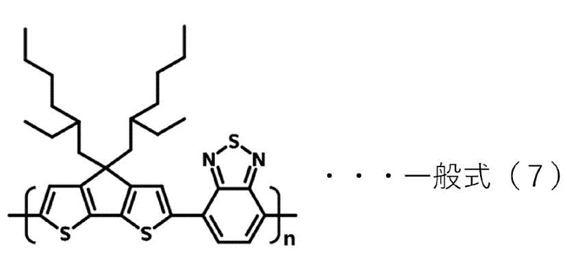
2,1,3-ベンゾチアジアゾール-チオフェン系共重合体とは、チオフェン骨格と2,1,3-ベンゾチアジアゾール骨格を主鎖に有する共役系共重合体を表す。2,1,3-ベンゾチアジアゾール-チオフェン系共重合体の具体例としては、下記一般式(5)~(8)などが挙げられる。なお、下記一般式(5)~(8)におけるnは、それぞれ独立して、1以上1000以下の整数を表す。 A 2,1,3-benzothiadiazole-thiophene-based copolymer represents a conjugated copolymer having a thiophene skeleton and a 2,1,3-benzothiadiazole skeleton in the main chain. Specific examples of the 2,1,3-benzothiadiazole-thiophene copolymer include the following general formulas (5) to (8). Each n in the following general formulas (5) to (8) independently represents an integer of 1 or more and 1000 or less.


キノキサリン-チオフェン系共重合体とは、チオフェン骨格とキノキサリン骨格を主鎖に有する共役系共重合体を表す。キノキサリン-チオフェン系共重合体の具体例としては、下記一般式(9)などが挙げられる。なお、下記一般式(9)におけるnは、1以上1000以下の整数を表す。 A quinoxaline-thiophene-based copolymer represents a conjugated copolymer having a thiophene skeleton and a quinoxaline skeleton in the main chain. Specific examples of the quinoxaline-thiophene copolymer include the following general formula (9). In addition, n in the following general formula (9) represents an integer of 1 or more and 1000 or less.

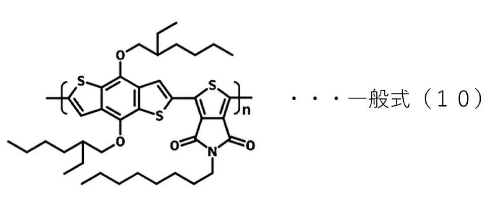
チオフェン-ベンゾジチオフェン系共重合体とは、チオフェン骨格とベンゾジチオフェン骨格を主鎖に有する共役系共重合体を表す。チオフェン-ベンゾジチオフェン系共重合体の具体例としては、下記一般式(10)~(13)などが挙げられる。なお、下記一般式(10)~(13)におけるnは、それぞれ独立して、1以上1000以下の整数を表す。 A thiophene-benzodithiophene-based copolymer represents a conjugated copolymer having a thiophene skeleton and a benzodithiophene skeleton in the main chain. Specific examples of the thiophene-benzodithiophene-based copolymer include the following general formulas (10) to (13). Each n in the following general formulas (10) to (13) independently represents an integer of 1 or more and 1000 or less.


-アクセプター性有機材料-
アクセプター性有機材料は、最低空軌道(LUMO)準位が3.5eV以上4.5eV以下であるπ電子共役化合物であることが好ましい。
-Acceptor Organic Materials-
The acceptor organic material is preferably a π-electron conjugated compound having a lowest unoccupied molecular orbital (LUMO) level of 3.5 eV or more and 4.5 eV or less.
アクセプター性有機材料としては、例えば、フラーレン又はその誘導体、ナフタレンテトラカルボン酸イミド誘導体、ペリレンテトラカルボン酸イミド誘導体などが挙げられる。これらの中でも、フラーレン誘導体が好ましい。
フラーレン誘導体としては、例えば、C60、フェニル-C61-酪酸メチル(公知文献等において、PCBM、[60]PCBM、又はPC61BMと記載されているフラーレン誘導体)、C70、フェニル-C71-酪酸メチル(公知文献等において、PCBM、[70]PCBM、又はPC71BMと記載されているフラーレン誘導体)、下記一般式(14)で表されるフラロピロリジン系フラーレン誘導体などが挙げられるが、下記一般式(14)で表されるフラロピロリジン系フラーレン誘導体であることが好ましい。
Acceptor organic materials include, for example, fullerenes or derivatives thereof, naphthalenetetracarboxylic acid imide derivatives, perylenetetracarboxylic acid imide derivatives, and the like. Among these, fullerene derivatives are preferred.
Examples of fullerene derivatives include C 60 , phenyl-C 61 -methyl butyrate (fullerene derivatives described as PCBM, [60]PCBM, or PC 61 BM in known literature), C 70 , phenyl-C 71 -Methyl butyrate (fullerene derivatives described as PCBM, [70]PCBM, or PC 71 BM in known documents, etc.), fulleropyrrolidine-based fullerene derivatives represented by the following general formula (14), etc. and a fulleropyrrolidine-based fullerene derivative represented by the following general formula (14).

上記一般式(14)中、Y1及びY2は、それぞれ独立して、水素原子、アルキル基、アルケニル基、アルキニル基、アリール基、又はアラルキル基を表す。但し、Y1及びY2が共に水素原子であることはない。また、上記のアルキル基、アルケニル基、アルキニル基、アリール基、及びアラルキル基はいずれも、置換基を有していても有していなくてもよい。 In general formula (14) above, Y 1 and Y 2 each independently represent a hydrogen atom, an alkyl group, an alkenyl group, an alkynyl group, an aryl group, or an aralkyl group. However, Y 1 and Y 2 are not both hydrogen atoms. Further, any of the above alkyl groups, alkenyl groups, alkynyl groups, aryl groups and aralkyl groups may or may not have a substituent.
Y1及びY2におけるアルキル基としては、炭素数1以上22以下のアルキル基が好ましく、炭素数1以上12以下のアルキル基がより好ましく、炭素数6以上12以下のアルキル基が更に好ましい。これらのアルキル基は、直鎖状及び分枝鎖状のいずれでもよいが、直鎖状であることが好ましい。なお、アルキル基には、炭素鎖中に更にS、Oなどの異種元素が1個又は2個以上含まれていてもよい。 As the alkyl group for Y 1 and Y 2 , an alkyl group having 1 to 22 carbon atoms is preferable, an alkyl group having 1 to 12 carbon atoms is more preferable, and an alkyl group having 6 to 12 carbon atoms is even more preferable. These alkyl groups may be linear or branched, but preferably linear. The alkyl group may further contain one or more different elements such as S and O in the carbon chain.
Y1及びY2におけるアルケニル基としては、炭素数2以上10以下のアルケニル基が好ましく、より好ましい具体例としては、ビニル基、1-プロペニル基、アリル基、イソプロペニル基、1-ブテニル基、2-ブテニル基、3-ブテニル基、1-メチル-2-プロペニル基、1,3-ブタジエニル基等の炭素数2以上4以下の直鎖状又は分岐鎖状アルケニル基を挙げることができる。 The alkenyl group for Y 1 and Y 2 is preferably an alkenyl group having 2 to 10 carbon atoms, and more preferred specific examples include a vinyl group, a 1-propenyl group, an allyl group, an isopropenyl group, a 1-butenyl group, Linear or branched alkenyl groups having 2 to 4 carbon atoms such as 2-butenyl group, 3-butenyl group, 1-methyl-2-propenyl group and 1,3-butadienyl group can be mentioned.
Y1及びY2におけるアルキニル基としては、炭素数1以上10以下のアルキニル基が好ましく、より好ましい具体例として、エチニル基、1-プロピニル基、2-プロピニル基、1-メチル-2-プロピニル基、1-ブチニル基、2-ブチニル基、3-ブチニル基等の炭素数2以上4以下の直鎖状又は分岐鎖状アルキニル基などが挙げられる。 The alkynyl group for Y 1 and Y 2 is preferably an alkynyl group having 1 to 10 carbon atoms, and more preferred specific examples include ethynyl, 1-propynyl, 2-propynyl and 1-methyl-2-propynyl groups. , 1-butynyl group, 2-butynyl group, 3-butynyl group, and the like, and linear or branched alkynyl groups having 2 to 4 carbon atoms.
Y1及びY2におけるアリール基としては、フェニル基、ナフチル基、アントラリル基、フェナントリル基などが挙げられる。 Examples of the aryl group for Y 1 and Y 2 include a phenyl group, naphthyl group, anthralyl group, and phenanthryl group.
Y1及びY2におけるアラルキル基としては、2-フェニルエチル、ベンジル、1-フェニルエチル、3-フェニルプロピル、4-フェニルブチル等の炭素数7以上20以下のアラルキル基などが挙げられる。 Examples of the aralkyl group for Y 1 and Y 2 include aralkyl groups having 7 to 20 carbon atoms such as 2-phenylethyl, benzyl, 1-phenylethyl, 3-phenylpropyl and 4-phenylbutyl.
Y1及びY2におけるアルキル基、アルケニル基、アルキニル基、アリール基、又はアラルキル基が置換基を有する場合、当該置換基の具体例としては、例えば、アルキル基、アルコキシカルボニル基、ポリエーテル基、アルカノイル基、アミノ基、アミノカルボニル基、アルコキシ基、アルキルチオ基、基:-CONHCOR’(ただし、式中、R’はアルキル基である)、基:-C(=NR’)-R”(ただし、式中、R’及びR”はアルキル基である)、基:-NR’=CR”R’”(ただし、式中、R’、R”及びR’”はアルキル基である)などが挙げられる。 When the alkyl group, alkenyl group, alkynyl group, aryl group, or aralkyl group in Y 1 and Y 2 has a substituent, specific examples of the substituent include an alkyl group, an alkoxycarbonyl group, a polyether group, Alkanoyl group, amino group, aminocarbonyl group, alkoxy group, alkylthio group, group: -CONHCOR' (wherein R' is an alkyl group), group: -C(=NR')-R" (where , wherein R′ and R″ are alkyl groups), the group —NR′═CR″R′″ (wherein R′, R″ and R′″ are alkyl groups), etc. mentioned.
Y1及びY2における置換基のうち、ポリエーテル基としては、例えば、式:Y3-(OY4)n-O-で表される基を例示できる。ここで、Y3はアルキル基等の一価の炭化水素基であり、Y4は、二価の脂肪族炭化水素基である。上記式で表されるポリエーテル基において、-(OY4)n-で表される繰り返し単位の具体例としては、-(OCH2)n-、-(OC2H4)n-、-(OC3H6)n-等のアルコキシ鎖が挙げられる。これらの繰り返し単位の繰り返し数nは、1以上20以下が好ましく、1以上5以下がより好ましい。-(OY4)n-で表される繰り返し単位には、同一の繰り返し単位だけではなく、2種以上の異なる繰り返し単位が含まれていてもよい。なお、上記繰り返し単位のうち、-OC2H4-及び-OC3H6-については、直鎖状及び分枝鎖状のいずれであってもよい。 Among the substituents for Y 1 and Y 2 , examples of polyether groups include groups represented by the formula: Y 3 —(OY 4 ) n —O—. Here, Y3 is a monovalent hydrocarbon group such as an alkyl group, and Y4 is a divalent aliphatic hydrocarbon group. Specific examples of the repeating unit represented by -(OY 4 ) n - in the polyether group represented by the above formula include -(OCH 2 ) n -, -(OC 2 H 4 ) n -, -( Alkoxy chains such as OC 3 H 6 ) n - are included. The repeating number n of these repeating units is preferably 1 or more and 20 or less, more preferably 1 or more and 5 or less. The repeating unit represented by -(OY 4 ) n - may contain not only the same repeating unit but also two or more different repeating units. Among the above repeating units, —OC 2 H 4 — and —OC 3 H 6 — may be linear or branched.
Y1及びY2における置換基のうち、アルキル基と、アルコキシカルボニル基、アルカノイル基、アルコキシ基、アルキルチオ基、ポリエーテル基、基:-CONHCOR’、基:-C(=NR’)-R”、及び基:-NR’=CR”R’”におけるアルキル基部分と、は炭素数1以上22以下のアルキル基が好ましく、炭素数1以上12以下のアルキル基がより好ましく、炭素数6以上12以下のアルキル基が更に好ましい。 Among the substituents in Y 1 and Y 2 , an alkyl group, an alkoxycarbonyl group, an alkanoyl group, an alkoxy group, an alkylthio group, a polyether group, a group: -CONHCOR', a group: -C(=NR')-R" , and the group: -NR'=CR"R'", the alkyl group portion is preferably an alkyl group having 1 to 22 carbon atoms, more preferably an alkyl group having 1 to 12 carbon atoms, and 6 to 12 carbon atoms. The following alkyl groups are more preferred.
Y1及びY2における置換基のうち、アミノ基と、アミノカルボニル基におけるアミノ基部分と、は炭素数1以上20以下のアルキル基が1個又は2個以上結合したアミノ基が好ましい。 Of the substituents for Y 1 and Y 2 , the amino group and the amino group moiety in the aminocarbonyl group are preferably amino groups to which one or more alkyl groups having 1 to 20 carbon atoms are bonded.
上記一般式(14)中、Arは、アリール基を表す。但し、アリール基は置換基を有していても有していなくてもよい。 In general formula (14) above, Ar represents an aryl group. However, the aryl group may or may not have a substituent.
Arのアリール基としては、フェニル基、ナフチル基、アントラリル基、フェナントリル基などが挙げられる。これらの中でも、フェニル基が好ましい。 Aryl groups for Ar include phenyl, naphthyl, anthralyl, and phenanthryl groups. Among these, a phenyl group is preferred.
Arのアリール基が置換基を有する場合、当該置換基の具体例としては、例えば、アリール基、アルキル基、シアノ基、アルコキシ基、アルコキシカルボニル基などが挙げられる。これらの置換基のうちのアリール基としては、フェニル基等を例示できる。また、これらの置換基のうちのアルキル基と、アルコキシ基のアルキル基部分と、は炭素数1以上22以下のアルキル基が好ましい。これらの置換基の数、及び置換位置については特に限定されないが、例えば、1個以上3個以下の置換基が任意の位置に存在することができる。 When the aryl group of Ar has a substituent, specific examples of the substituent include an aryl group, an alkyl group, a cyano group, an alkoxy group, and an alkoxycarbonyl group. Examples of the aryl group among these substituents include a phenyl group and the like. Moreover, the alkyl group among these substituents and the alkyl group portion of the alkoxy group are preferably alkyl groups having 1 or more and 22 or less carbon atoms. Although the number of these substituents and the substitution positions are not particularly limited, for example, 1 or more and 3 or less substituents can exist at arbitrary positions.
-光電変換層の平均厚み-
光電変換層の平均厚みは、50nm以上400nm以下であることが好ましく、60nm以上250nm以下であることがより好ましい。平均厚みが50nm以上であることで、光電変換層の光吸収による生じるキャリア量が十分となる。また、平均厚みが400nm以下であることで、光吸収により生じるキャリアの輸送効率低下が抑制される。
光電変換層の平均厚みは、例えば、次のような方法により光電変換層の厚みを無作為に9点で測定し、これらの平均値を求めることで算出される。まず、基材上に光電変換層を構成する材料を含む液体を塗布して乾燥させた後、溶剤で任意の点ふき取り、Bruker社製DEKTAKを用い、ふき取った場所の段差の高さを測定し、得られた測定値を厚みとする。なお、光電変換素子の断面を走査型電子顕微鏡(SEM)又は透過型電子顕微鏡(TEM)を用いて観察することにより、光電変換層の平均厚みを測定してもよい。
-Average thickness of photoelectric conversion layer-
The average thickness of the photoelectric conversion layer is preferably 50 nm or more and 400 nm or less, more preferably 60 nm or more and 250 nm or less. When the average thickness is 50 nm or more, the amount of carriers generated by light absorption in the photoelectric conversion layer becomes sufficient. In addition, since the average thickness is 400 nm or less, a decrease in carrier transport efficiency caused by light absorption is suppressed.
The average thickness of the photoelectric conversion layer is calculated, for example, by randomly measuring the thickness of the photoelectric conversion layer at 9 points by the following method and calculating the average value of these measurements. First, a liquid containing a material that constitutes the photoelectric conversion layer was applied onto the base material and dried, then any points were wiped off with a solvent, and the height of the step at the location where the wiping was performed was measured using DEKTAK manufactured by Bruker. , the obtained measured value is taken as the thickness. The average thickness of the photoelectric conversion layer may be measured by observing the cross section of the photoelectric conversion element with a scanning electron microscope (SEM) or transmission electron microscope (TEM).
-光電変換層におけるバルクへテロ接合の形成方法-
光電変換層は、上記の各有機材料を順次積層して平面的な接合界面を有する層としてもよいが、接合界面の面積を大きくするため、上記の各有機材料が三次元的に混在した構造を有するバルクへテロ接合を形成させることが好ましい。バルクヘテロ接合は、例えば、次のようにして形成する。
各有機材料が溶解性の高い材料である場合は、各有機材料を溶剤に溶かし、各有機材料が分子状で混合された溶液を作製し、塗布後に乾燥させて溶剤を除去することで形成する。この場合、更に加熱処理を行うことで各有機材料の凝集状態を最適化してもよい。
一方で、溶解性の低い有機材料を用いる場合は、一方の有機材料が溶解した溶液に他方の有機材料を分散させた液体を作製し、塗布後に乾燥させて溶剤を除去することで形成する。この場合、更に加熱処理を行うことで各有機材料の凝集状態を最適化してもよい。
-Method for Forming Bulk Heterojunction in Photoelectric Conversion Layer-
The photoelectric conversion layer may be a layer having a planar bonding interface by sequentially laminating each of the above organic materials. However, in order to increase the area of the bonding interface, the above organic materials are three-dimensionally mixed. It is preferred to form a bulk heterojunction with A bulk heterojunction is formed, for example, as follows.
When each organic material is a highly soluble material, each organic material is dissolved in a solvent to prepare a solution in which each organic material is mixed in a molecular form, and then dried to remove the solvent after coating. . In this case, the aggregation state of each organic material may be optimized by further performing heat treatment.
On the other hand, when using an organic material with low solubility, a liquid is prepared by dispersing the other organic material in a solution in which one organic material is dissolved, and the liquid is dried after coating to remove the solvent. In this case, the aggregation state of each organic material may be optimized by further performing heat treatment.
-光電変換層の作製方法-
光電変換層の作製方法は、上記の各有機材料を含有する液体を付与する工程などを有する。付与方法としては、例えば、スピンコート法、ブレードコート法、スリットダイコート法、スクリーン印刷法、バーコーター法、鋳型法、印刷転写法、浸漬引き上げ法、インクジェット法、スプレー法、真空蒸着法などが挙げられる。これらの中から、厚み制御や配向制御など、作製しようとする光電変換層の特性に応じて適宜選択する。
-Method for producing photoelectric conversion layer-
A method for producing a photoelectric conversion layer includes a step of applying a liquid containing each of the above organic materials. Application methods include, for example, spin coating, blade coating, slit die coating, screen printing, bar coating, casting, printing transfer, immersion and pulling, inkjet, spraying, and vacuum deposition. be done. From these, it is appropriately selected according to the characteristics of the photoelectric conversion layer to be produced, such as thickness control and orientation control.
例えば、スピンコート法を用いる場合、上記の各有機材料を5mg/mL以上40mg/mL以下の濃度で含有する溶液を用いることが好ましい。なお、濃度とは、各有機材料を含む溶液の体積に対する各有機材料の合計質量を表す。上記濃度に設定することで均質な光電変換層を容易に作製することができる。 For example, when spin coating is used, it is preferable to use a solution containing each of the above organic materials at a concentration of 5 mg/mL or more and 40 mg/mL or less. Note that the concentration represents the total mass of each organic material with respect to the volume of the solution containing each organic material. A homogeneous photoelectric conversion layer can be easily produced by setting the above concentration.
また、付与された各有機材料を含む液体から溶媒又は分散媒を除去するために、減圧下又は不活性雰囲気下(窒素、アルゴン雰囲気下)においてアニーリング処理を行ってもよい。アニーリング処理の温度は、40℃以上300℃以下であることが好ましく、50℃以上150℃以下であることがより好ましい。なお、アニーリング処理を行うことで、積層した層間の界面において、各層を構成する材料が互いに浸透することで接触面積が増加し、短絡電流を増大させることができる場合があるため好ましい。 Further, annealing may be performed under reduced pressure or in an inert atmosphere (nitrogen or argon atmosphere) in order to remove the solvent or dispersion medium from the applied liquid containing each organic material. The temperature of the annealing treatment is preferably 40° C. or higher and 300° C. or lower, and more preferably 50° C. or higher and 150° C. or lower. Annealing treatment is preferable because the materials constituting each layer permeate each other at the interface between the laminated layers, thereby increasing the contact area and increasing the short-circuit current.
各有機材料を溶解又は分散させる溶媒又は分散媒としては、例えば、メタノール、エタノール、ブタノール、トルエン、キシレン、o-クロロフェノール、アセトン、酢酸エチル、エチレングリコール、テトラヒドロフラン、ジクロロメタン、クロロホルム、ジクロロエタン、クロロベンゼン、ジクロロベンゼン、トリクロロベンゼン、オルトジクロロベンゼン、クロロナフタレン、ジメチルホルムアミド、ジメチルスルホキシド、N-メチルピロリドン、及びγ-ブチロラクトンなどが挙げられる。これらは、1種単独で使用してもよいし、2種以上を併用してもよい。また、これらの中でも、クロロベンゼン、クロロホルム、オルトジクロロベンゼンが特に好ましい。
なお、上記溶媒又は分散媒には各種添加剤を含有させてもよい。各種添加剤としては、例えば、ジヨードオクタン、オクタンジチオール等を用いることができる。
Examples of solvents or dispersion media for dissolving or dispersing each organic material include methanol, ethanol, butanol, toluene, xylene, o-chlorophenol, acetone, ethyl acetate, ethylene glycol, tetrahydrofuran, dichloromethane, chloroform, dichloroethane, chlorobenzene, Dichlorobenzene, trichlorobenzene, ortho-dichlorobenzene, chloronaphthalene, dimethylformamide, dimethylsulfoxide, N-methylpyrrolidone, γ-butyrolactone and the like. These may be used individually by 1 type, and may use 2 or more types together. Among these, chlorobenzene, chloroform, and ortho-dichlorobenzene are particularly preferred.
The solvent or dispersion medium may contain various additives. Examples of various additives that can be used include diiodooctane and octanedithiol.
<正孔輸送層>
「正孔輸送層」とは、光電変換層で生じた正孔を輸送し、光電変換層で生じた電子の侵入を抑制する層である。正孔輸送層は、1層からなる構造でもよいし、2層以上有する構造であってもよい。以下、一例として、正孔輸送層を1層有する構造である場合について説明する。
<Hole transport layer>
The “hole transport layer” is a layer that transports holes generated in the photoelectric conversion layer and suppresses penetration of electrons generated in the photoelectric conversion layer. The hole transport layer may have a structure consisting of one layer, or may have a structure having two or more layers. As an example, a structure having one hole transport layer will be described below.
正孔輸送層は、正孔輸送性を有する有機化合物及び無機化合物から選ばれる少なくとも1つを含有する層であることが好ましい。正孔輸送性を有する有機化合物としては、PEDOT:PSS(ポリエチレンジオキシチオフェン:ポリスチレンスルホン酸)等の導電性高分子、及び芳香族アミン誘導体などが挙げられる。正孔輸送性を有する無機化合物としては、酸化モリブデン、酸化タングステン、酸化バナジウム、酸化ニッケル、及び酸化銅(I)などが挙げられる。これら正孔輸送性を有する化合物の中でも、酸化モリブデン、酸化タングステン、及び酸化バナジウムが好ましい。 The hole-transporting layer is preferably a layer containing at least one selected from organic compounds and inorganic compounds having hole-transporting properties. Organic compounds having hole-transport properties include conductive polymers such as PEDOT:PSS (polyethylenedioxythiophene:polystyrenesulfonic acid), aromatic amine derivatives, and the like. Examples of inorganic compounds having hole-transport properties include molybdenum oxide, tungsten oxide, vanadium oxide, nickel oxide, and copper (I) oxide. Among these hole-transporting compounds, molybdenum oxide, tungsten oxide, and vanadium oxide are preferred.
正孔輸送層の平均厚みは、200nm以下であることが好ましく、1nm以上50nm以下であることがより好ましい。 The average thickness of the hole transport layer is preferably 200 nm or less, more preferably 1 nm or more and 50 nm or less.
正孔輸送層の製造方法としては、例えば、正孔輸送性を有する化合物と溶媒又は分散媒とを含む液体を塗布して乾燥させる方法が挙げられる。塗布方法としては、スピンコート法、ゾルゲル法、スリットダイコート法、及びスパッタリング法などが挙げられる。 Examples of the method for producing the hole transport layer include a method of applying and drying a liquid containing a compound having a hole transport property and a solvent or a dispersion medium. Examples of coating methods include a spin coating method, a sol-gel method, a slit die coating method, a sputtering method, and the like.
<第二の電極>
「第二の電極」とは、光電変換されて生じた正孔を捕集する電極である。第二の電極が光の入射面側に設けられている場合、第二の電極は、光電変換効率を高める観点から光透過性が高いことが好ましく、透明であることがより好ましい。但し、第二の電極が光の入射面の反対側に設けられている場合、光透過性及び透明性が低くてもよい。
第二の電極は、上記の第一の電極と同様のものを用いることができるため説明を省略する。
<Second electrode>
The “second electrode” is an electrode that collects holes generated by photoelectric conversion. When the second electrode is provided on the light incident surface side, the second electrode preferably has high light transmittance from the viewpoint of increasing the photoelectric conversion efficiency, and is more preferably transparent. However, when the second electrode is provided on the opposite side of the light incident surface, the light transmittance and transparency may be low.
Since the second electrode can be the same as the first electrode, the description thereof is omitted.
<表面保護層(パッシベーション層)>
「表面保護層」とは、光の入射面の反対側に設けられている電極と封止部材とが直接接触することを防止する層である。また、表面保護層は、光の入射面の反対側に設けられている電極に加え、積層されている各層の露出面が封止部材と直接接触することを防止するように設けられている部材であってもよい。なお、表面保護層は、パッシベーション層とも称される。
<Surface protective layer (passivation layer)>
The “surface protective layer” is a layer that prevents direct contact between the electrode provided on the opposite side of the light incident surface and the sealing member. In addition to the electrode provided on the opposite side of the light incident surface, the surface protective layer is a member provided so as to prevent the exposed surfaces of the laminated layers from directly contacting the sealing member. may be Note that the surface protective layer is also called a passivation layer.
表面保護層の材料としては、例えば、SiOx、SiOxNy、Al2O3等の金属酸化物、ポリエチレン、フッ素系コーティング剤、ポリパラキシリレン等のポリマーなどが挙げられる。これらは、1種単独で使用してもよいし、2種以上を併用してもよい。これらの中でも、金属酸化物又はフッ素系コーティング剤が好ましい。 Examples of materials for the surface protective layer include metal oxides such as SiOx, SiOxNy, and Al2O3 , polyethylene, fluorine-based coating agents, and polymers such as polyparaxylylene. These may be used individually by 1 type, and may use 2 or more types together. Among these, metal oxides or fluorine-based coating agents are preferred.
表面保護層の平均厚みは、1nm以上10μm以下であることが好ましい。 The average thickness of the surface protective layer is preferably 1 nm or more and 10 μm or less.
表面保護層の製造方法としては、例えば、真空蒸着法、スパッタリング法、反応性スパッタリング法、MBE(分子線エピタキシ)法、プラズマCVD法、レーザーCVD法、熱CVD法、ガスソースCVD法、コーティング法、印刷法、転写法などが挙げられる。 Examples of methods for producing the surface protective layer include vacuum deposition, sputtering, reactive sputtering, MBE (molecular beam epitaxy), plasma CVD, laser CVD, thermal CVD, gas source CVD, and coating. , a printing method, a transfer method, and the like.
<封止部材>
「封止部材」とは、水および酸素などの外部物質が光電変換素子内部(具体的には、少なくとも封止部材及び他方の電極で形作られる空間内)へ侵入して上記各層と接触することを抑制する部材である。封止部材は、外部物質が光電変換素子内部へ侵入することを抑制するガスバリア部材及び他方の電極における接着領域と接着する接着部材を有することが好ましく、これら部材が一体化したフィルム状の部材であることがより好ましい。また、封止部材は、一方の電極を被覆するように設けられている。なお、封止部材が光の入射面の反対側に設けられている場合、封止部材は光透過性又は透明性を有していなくてもよい。
<Sealing member>
The “sealing member” means that external substances such as water and oxygen enter the inside of the photoelectric conversion element (specifically, the space formed by at least the sealing member and the other electrode) and come into contact with the above layers. It is a member that suppresses The sealing member preferably has a gas barrier member that suppresses the intrusion of external substances into the photoelectric conversion element and an adhesive member that adheres to the adhesive region of the other electrode. It is more preferable to have Also, the sealing member is provided so as to cover one of the electrodes. In addition, when the sealing member is provided on the opposite side of the light incident surface, the sealing member does not have to be light transmissive or transparent.
ガスバリア部材に要求される機能は、一般的に水蒸気透過量及び酸素透過量などで表現される。JIS K7129 B法準拠に準拠する一日あたりの水蒸気透過量は、例えば、1×10⁻²g/m2以下であることが好ましく、低ければ低いほど好ましい。また、JIS K7126-2に準拠する一日あたりの酸素透過量は、例えば、1cm3/m2・atm以下であることが好ましく、低ければ低いほど好ましい。 The functions required of the gas barrier member are generally expressed by the amount of water vapor permeation, the amount of oxygen permeation, and the like. The water vapor permeation amount per day conforming to JIS K7129 B method is preferably, for example, 1×10 −2 g/m 2 or less, and the lower the better. In addition, the oxygen permeation amount per day according to JIS K7126-2 is preferably, for example, 1 cm 3 /m 2 ·atm or less, and the lower the better.
ガスバリア部材の材料は、例えば、金属箔、金属箔に樹脂材料を積層したフィルム、SiO2などの無機材料と有機材料を積層させた構造を有するフィルム、及びガラスなどが挙げられる。 Materials for the gas barrier member include, for example, metal foil, a film obtained by laminating a resin material on a metal foil, a film having a structure obtained by laminating an inorganic material such as SiO 2 and an organic material, and glass.
接着部材の材料は、例えば、有機電界発光素子及び有機トランジスタ等の封止に用いられる一般的な材料を使用することができる。具体的には、感圧接着性樹脂、熱硬化性樹脂、熱可塑性樹脂、光硬化性樹脂などが挙げられる。これらの中でも、封止工程で加熱する必要がない感圧接着性樹脂又は低温加熱で接着可能な樹脂が好ましい。より具体的には、エポキシ系樹脂、ポリオレフィン系樹脂、エチレン-酢酸ビニル共重合体樹脂、スチレン-イソブチレン樹脂、ポリエステル系樹脂、アクリル系樹脂、ウレタン系樹脂、シリコーン系樹脂などが挙げられるが、接着性を向上させる観点からエポキシ系樹脂又はポリオレフィン系樹脂が好ましい。これら樹脂の主鎖、分岐鎖、末端における化学修飾、分子量の調整等によって、各種接着特性を得ることができる。なお、接着部材は、上記樹脂に加えて、吸湿性の材料又はハイドロタルサイトなどが含まれていてもよい。 As the material of the adhesive member, for example, general materials used for encapsulation of organic electroluminescence elements, organic transistors, and the like can be used. Specific examples include pressure-sensitive adhesive resins, thermosetting resins, thermoplastic resins, and photocurable resins. Among these, a pressure-sensitive adhesive resin which does not need to be heated in the sealing step or a resin which can be adhered by heating at a low temperature is preferable. More specific examples include epoxy resins, polyolefin resins, ethylene-vinyl acetate copolymer resins, styrene-isobutylene resins, polyester resins, acrylic resins, urethane resins, and silicone resins. Epoxy-based resins or polyolefin-based resins are preferred from the viewpoint of improving the properties. Various adhesive properties can be obtained by chemically modifying the main chain, branched chains and terminals of these resins, adjusting the molecular weight, and the like. The adhesive member may contain a hygroscopic material, hydrotalcite, or the like in addition to the above resin.
<UVカット層>
「UVカット層」とは、光の入射面側に設けられ、UV光による光電変換素子の劣化を抑制する層である。UVカット層は、UV光を吸収するフィルム状の部材であることが好ましい。また、UVカット層は、光の入射面側に位置する基材上に設けられていることが好ましい。
<UV cut layer>
The “UV cut layer” is a layer that is provided on the light incident surface side and suppresses deterioration of the photoelectric conversion element due to UV light. The UV cut layer is preferably a film-like member that absorbs UV light. Moreover, it is preferable that the UV cut layer is provided on the substrate located on the light incident surface side.
UVカット層に要求される機能は、一般的に光透過率などで表現される。波長370nm以下の光に対する光透過率は、例えば、1%未満であることが好ましい。また、波長410nm以下の光に対する光透過率は、例えば、1%未満であることが好ましい。 The functions required of the UV cut layer are generally expressed in terms of light transmittance and the like. The light transmittance for light with a wavelength of 370 nm or less is preferably less than 1%, for example. Also, the light transmittance for light with a wavelength of 410 nm or less is preferably less than 1%, for example.
<ガスバリア層>
「ガスバリア層」とは、水および酸素などの外部物質が光電変換素子内部へ侵入することを抑制する層である。ガスバリア層は、連続膜であることが好ましい。また、ガスバリア層は、基材と隣接して設けられることが好ましく、他方の電極と基材との間に設けられることがより好ましい。なお、ガスバリア層が基材と隣接して設けられている場合、本開示では、ガスバリア層を、基材を構成する一構成とみなす。
<Gas barrier layer>
A "gas barrier layer" is a layer that prevents external substances such as water and oxygen from penetrating into the photoelectric conversion element. The gas barrier layer is preferably a continuous film. Also, the gas barrier layer is preferably provided adjacent to the substrate, and more preferably provided between the other electrode and the substrate. In the present disclosure, when the gas barrier layer is provided adjacent to the substrate, the gas barrier layer is regarded as one component of the substrate.
ガスバリア層に要求される機能は、一般的に水蒸気透過量及び酸素透過量などで表現される。JIS K7129 B法に準拠する一日あたりの水蒸気透過量は、例えば、1×10⁻²g/m2以下であることが好ましく、低ければ低いほど好ましい。また、JIS K7126-2に準拠する一日あたりの酸素透過量は、例えば、1cm3/m2・atm以下であることが好ましく、低ければ低いほど好ましい。 The functions required of the gas barrier layer are generally expressed by the amount of water vapor permeation, the amount of oxygen permeation, and the like. The water vapor permeation amount per day according to JIS K7129 B method is preferably, for example, 1×10 −2 g/m 2 or less, and the lower the better. In addition, the oxygen permeation amount per day according to JIS K7126-2 is preferably, for example, 1 cm 3 /m 2 ·atm or less, and the lower the better.
ガスバリア層の材料としては、例えば、SiO2、SiNx、Al2O3、SiC、SiCN、SiOC、SiOAlを含む材料、及びシロキサン系材料などが挙げられる。 Materials for the gas barrier layer include, for example, materials containing SiO 2 , SiNx, Al 2 O 3 , SiC, SiCN, SiOC, and SiOAl, and siloxane-based materials.
<その他の層>
光電変換素子は、更に必要に応じて、絶縁性多孔質層、劣化防止層、保護層などのその他の層を有してもよい。
<Other layers>
The photoelectric conversion element may further have other layers such as an insulating porous layer, a deterioration preventing layer, and a protective layer, if necessary.
<光電変換素子の構成> <Structure of photoelectric conversion element>
光電変換素子の構成の一例について図1~2を用いて説明する。図1は、光電変換素子の一例を示す俯瞰概略図である。図2は、光電変換素子の一例を示す断面概略図である。 An example of the configuration of a photoelectric conversion element will be described with reference to FIGS. 1 and 2. FIG. FIG. 1 is a schematic bird's-eye view showing an example of a photoelectric conversion element. FIG. 2 is a schematic cross-sectional view showing an example of a photoelectric conversion element.
図1の俯瞰概略図に示す通り、光電変換素子1は、光電変換可能な領域である光電変換領域2、光電変換領域2を取り囲む封止領域3、及び端子等のその他部材が設けられたその他領域4を有する。
As shown in the schematic bird's-eye view of FIG. 1, the
図2の断面概略図に示す通り、光電変換素子1は、光電変換領域2において、積層方向zに沿って、光の入射面側から順に、UVカット層11、基材12、第一の電極13、第一の電子輸送層14、第二の電子輸送層(中間層)15、光電変換層16、正孔輸送層17、第二の電極18、表面保護層(パッシベーション層)19、及び封止部材20を積層した構造(以降、「構造A」とも称する)を有する。また、光電変換素子1は、封止領域3において、積層方向zに沿って、光の入射面側から順に、UVカット層11、基材12、第一の電極13、及び封止部材20を積層した構造を有する。このとき、封止部材20は、接着部材21及びガスバリア部材22を有する。また、封止部材20は、第一の電子輸送層14、第二の電子輸送層(中間層)15、光電変換層16、正孔輸送層17、第二の電極18、及び表面保護層(パッシベーション層)19を内包し、且つ第一の電極13における接着領域30と接着している。なお、光電変換素子1において、第一の電極13は上記の「他方の電極」に相当し、第二の電極18は上記の「一方の電極」に相当する。また、光電変換素子1は、更に、別の光電変換素子と直列又は並列に電気的に接続されるための接続部などを有していてもよい。また、積層方向zは、光電変換素子における各層の面(xy面)に対して垂直な方向を表す。
As shown in the schematic cross-sectional view of FIG. 2, the
なお、構造Aを有する光電変換素子1の光電変換領域2における第一の電極13から第二の電極18までの積層順は、上記の通り、この順に限られない。具体的には、光電変換素子1は、光電変換領域2において、積層方向zに沿って、光の入射面側から順に、UVカット層11、基材12、第二の電極13、正孔輸送層14、光電変換層15、第二の電子輸送層(中間層)16、第一の電子輸送層17、第一の電極18、表面保護層(パッシベーション層)19、及び封止部材20を積層した構造(以降、「構造B」とも称する)であってもよい。このとき、封止部材20は、正孔輸送層14、光電変換層15、第二の電子輸送層(中間層)16、第一の電子輸送層17、第一の電極18、及び表面保護層(パッシベーション層)19を内包し、且つ第二の電極13における接着領域30と接着している。なお、光電変換素子1において、第二の電極13は上記の「他方の電極」に相当し、第一の電極18は上記の「一方の電極」に相当する。
本開示では、図1~2に示す通り、構造Aを有する光電変換素子を一例として主に説明するが、当業者であれば、かかる説明から構造Bを有する光電変換素子について容易に理解できる。
As described above, the stacking order from the
In the present disclosure, as shown in FIGS. 1 and 2, the photoelectric conversion element having structure A will be mainly described as an example, but those skilled in the art can easily understand the photoelectric conversion element having structure B from this description.
次に、封止部材20及び第一の電極13(他方の電極)の接着態様について図3を用いて説明する。図3は、光電変換素子の接着領域近傍における構造の一例を示す断面概略図である。
Next, the adhesion state of the sealing
接着領域30近傍を拡大した図3の断面概略図に示す通り、封止部材20の接着部材21及び第一の電極13(他方の電極)が直接的に又は間接的に接触することで接着している。接着部材21及び第一の電極13(他方の電極)の接着態様としては、理想的には、接着部材21及び第一の電極13(他方の電極)が直接接触して接着していることが好ましいが、実際は、図3に示す通り、光電変換素子1の製造工程上の都合により、いずれかの層を形成していた材料などに由来する付着物23を介して接着部材21及び第一の電極13(他方の電極)が間接的に接着している場合がある。また、接着部材21及び第一の電極13(他方の電極)が直接接触して接着している場合であったとしても、図3に示す通り、光電変換素子1の製造工程上の都合により、部分的に削られた第一の電極13(他方の電極)における凹部及び接着部材21が接着している場合もある。このように、接着部材21及び第一の電極13(他方の電極)の接着界面が凹凸を有する場合、接着部材21が第一の電極13(他方の電極)と十分に接着することが困難になる部分が発生する頻度が高まり、封止部材20の封止性能が低下し、結果として、光電変換素子が高温高湿環境下に長時間置かれることで光電変換効率が低下する課題が生じる。
As shown in the schematic cross-sectional view of FIG. 3 in which the vicinity of the
上記課題に対し、封止部材20の封止性能を向上させる手法としては、光電変換素子1の積層方向zを含む断面において、第一の電極13(他方の電極)における接着領域30を有さない面31から接着領域30と接着している封止部材21までの積層方向zにおける長さLの最大値Lmax及び最小値Lminの差を1000nm以下にすることが有効であり、500nm以下にすることが好ましく、100nm以下にすることがより好ましい。1000nm以下であることで、接着部材21及び第一の電極13(他方の電極)の接着界面における凹凸の程度が小さくなり、封止部材20の封止性能が向上する。一方で、長さLの最大値Lmax及び最小値Lminの差は、20nm以上であることが好ましい。20nm以上であることで、凹凸により接着部材21及び第一の電極13(他方の電極)の間でアンカー効果が生じ、封止部材20の封止性能が向上する。
なお、光電変換素子1の積層方向zを含む断面は封止領域3(接着領域30を含む範囲)において作成する。また、長さLは、断面内の積層方向zと直行する方向(例えば、y方向)において2.5μmの長さの評価区間Eを設定し、評価区間E内において測定する。すなわち、評価区間E内における長さLの最大値がLmaxであり、長さLの最小値がLminであり、このLmax及びLminから上記差を算出する。また、評価区間Eにおいて、接着部材21及び第一の電極13(他方の電極)の接着界面に空隙が存在する場合、長さLは、面31から封止部材21までの積層方向zにおける長さから空隙部分の積層方向zにおける長さを差し引いた長さであるとする。また、評価区間Eは、封止領域3の外周部より100μm以上内側の領域であってかつ封止領域3の内周部より100μm以上内側の領域において設定する。また、上記の差は、異なる3箇所以上の評価区間でそれぞれ算出された差の平均値を採用する。
As a method for improving the sealing performance of the sealing
A cross section including the stacking direction z of the
長さLの最大値Lmax及び最小値Lminの差が1000nm以下である場合、上記の通り、光電変換素子が高温高湿環境下に長時間置かれたとしても光電変換効率の低下が抑制される。光電変換効率の低下が抑制されるとは、具体的には、光電変換素子を40℃、90%Rh環境下に500時間静置する試験を行った場合において、光電変換効率の維持率が80%以上であることを表す。なお、光電変換効率の維持率とは、試験前の光電変換効率に対する試験後の光電変換効率の割合を表す。 When the difference between the maximum value L max and the minimum value L min of the length L is 1000 nm or less, as described above, even if the photoelectric conversion element is placed in a high temperature and high humidity environment for a long time, the decrease in photoelectric conversion efficiency is suppressed. be done. Suppressing a decrease in photoelectric conversion efficiency specifically means that the photoelectric conversion efficiency maintenance rate is 80 in a test in which the photoelectric conversion element is left in an environment of 40° C. and 90% Rh for 500 hours. % or more. Note that the maintenance rate of the photoelectric conversion efficiency represents the ratio of the photoelectric conversion efficiency after the test to the photoelectric conversion efficiency before the test.
<<光電変換モジュール>>
「光電変換モジュール」とは、電気的に接続されている複数の光電変換素子を有するものである。電気的な接続は、光電変換素子が直列に接続されている場合及び並列に接続されている場合のいずれであってもよい。また、光電変換モジュールは、直列に接続されている複数の光電変換素子および並列に接続されている複数の光電変換素子の両方を有していてもよい。なお、本開示における「接続」は、いずれも、物理的な接続に限定されず、電気的な接続も含まれるものとする。
<<Photoelectric conversion module>>
A “photoelectric conversion module” has a plurality of electrically connected photoelectric conversion elements. The electrical connection may be either serial connection or parallel connection of the photoelectric conversion elements. Moreover, the photoelectric conversion module may have both a plurality of photoelectric conversion elements connected in series and a plurality of photoelectric conversion elements connected in parallel. Note that "connection" in the present disclosure is not limited to physical connection, and includes electrical connection.
光電変換モジュールは、複数の光電変換素子と、光電変換素子間を電気的に接続する接続部と、を有し、必要に応じてその他部材を有する。言い換えると、光電変換モジュールは、少なくとも、第一の光電変換素子と、第二の光電変換素子と、第一の光電変換素子及び第二の光電変換素子を電気的に接続する接続部と、を有し、必要に応じてその他部材を有する。なお、光電変換素子および接続部は、機能上区別される部材であればよく、光電変換素子および接続部がそれぞれ独立した部材であってもよいが、光電変換素子および接続部が連続的または一体的に設けられた部材であってもよい。例えば、光電変換素子の一構成である電極等と接続部とが、それぞれ独立した部材であってもよいが、連続的または一体的に設けられた部材であってもよい。 A photoelectric conversion module includes a plurality of photoelectric conversion elements, a connecting portion that electrically connects the photoelectric conversion elements, and other members as necessary. In other words, the photoelectric conversion module includes at least a first photoelectric conversion element, a second photoelectric conversion element, and a connection portion that electrically connects the first photoelectric conversion element and the second photoelectric conversion element. and other members as necessary. Note that the photoelectric conversion element and the connection portion may be functionally distinct members, and the photoelectric conversion element and the connection portion may be independent members. It may be a member that is provided on purpose. For example, the electrodes and the like, which are one component of the photoelectric conversion element, and the connection portion may be independent members, or may be members provided continuously or integrally.
<<光電変換素子、光電変換モジュールの製造方法>>
光電変換モジュールの製造方法の一例について説明することで、同時に、光電変換素子の製造方法の一例についても説明する。なお、本開示では、図2に示すような構造Aを有する光電変換素子の製造方法の一例について説明するが、当業者であれば、かかる説明から構造Bを有する光電変換素子の製造方法の一例について容易に理解できる。
<<Method for Manufacturing Photoelectric Conversion Element and Photoelectric Conversion Module>>
By describing an example of a method for manufacturing a photoelectric conversion module, an example of a method for manufacturing a photoelectric conversion element will also be described at the same time. In the present disclosure, an example of a method for manufacturing a photoelectric conversion element having structure A as shown in FIG. 2 will be described. can be easily understood.
光電変換素子を有する光電変換モジュールの製造方法は、例えば、基材上にガスバリア層を形成するガスバリア層形成工程と、ガスバリア層を有する基材上に第一の電極を形成する第一の電極形成工程と、第一の電極上に電子輸送層を形成する電子輸送層形成工程と、電子輸送層上に光電変換層を形成する光電変換層形成工程と、電子輸送層及び光電変換層を貫通する貫通部を形成する貫通部形成工程と、光電変換層上に正孔輸送層を形成し且つ貫通部における第一の電極、電子輸送層、及び光電変換層の露出表面を正孔輸送層の材料で被覆する正孔輸送層形成工程と、正孔輸送層上に第二の電極を形成し且つ貫通部を第二の電極の材料で充填して貫通構造を形成する第二の電極形成工程と、第二の電極上に表面保護層を形成する表面保護層形成工程と、電子輸送層から表面保護層までの積層物における外周部を除去することで第一の電極における接着領域を形成する接着領域形成工程と、封止部材に電子輸送層から表面保護層までの積層物を内包させ且つ接着領域と接触させる封止部材形成工程とを有し、必要に応じて、UVカット層形成工程などのその他工程等を有する。 A method for manufacturing a photoelectric conversion module having a photoelectric conversion element includes, for example, a gas barrier layer forming step of forming a gas barrier layer on a base material, and a first electrode forming step of forming a first electrode on the base material having the gas barrier layer. an electron transport layer forming step of forming an electron transport layer on the first electrode; a photoelectric conversion layer forming step of forming a photoelectric conversion layer on the electron transport layer; a through portion forming step of forming a through portion; forming a hole transport layer on the photoelectric conversion layer; and a second electrode forming step of forming a second electrode on the hole transport layer and filling the through portion with the material of the second electrode to form a through structure. a surface protective layer forming step of forming a surface protective layer on the second electrode; It has a region forming step and a sealing member forming step in which the laminate from the electron transport layer to the surface protective layer is included in the sealing member and is brought into contact with the adhesion region, and if necessary, a UV cut layer forming step, etc. Other processes, etc.
<ガスバリア層形成工程>
光電変換素子を有する光電変換モジュールの製造方法は、基材上にガスバリア層を形成するガスバリア層形成工程を有することが好ましい。なお、基材自体がガスバリア性を有する場合、ガスバリア層は形成しなくてもよい。
<Gas barrier layer forming step>
A method for manufacturing a photoelectric conversion module having photoelectric conversion elements preferably includes a gas barrier layer forming step of forming a gas barrier layer on a substrate. In addition, when the base material itself has gas barrier properties, the gas barrier layer may not be formed.
<第一の電極形成工程>
光電変換素子を有する光電変換モジュールの製造方法は、ガスバリア層を有する基材上に第一の電極を形成する第一の電極形成工程を有することが好ましい。なお、基材がガスバリア層を有さない場合は、基材上に第一の電極を形成してもよい。
第一の電極を形成する方法は、第一の電極に関する説明において記載した通りである。
<First electrode forming step>
A method for manufacturing a photoelectric conversion module having photoelectric conversion elements preferably includes a first electrode forming step of forming a first electrode on a substrate having a gas barrier layer. In addition, when the substrate does not have a gas barrier layer, the first electrode may be formed on the substrate.
The method of forming the first electrode is as described in the description of the first electrode.
<電子輸送層形成工程>
光電変換素子を有する光電変換モジュールの製造方法は、第一の電極上に電子輸送層を形成する電子輸送層形成工程を有することが好ましい。また、電子輸送層として第一の電子輸送層および第二の電子輸送層(中間層)を有する場合は、電子輸送層形成工程は、第一の電極上に第一の電子輸送層を形成する第一の電子輸送層形成工程と、第一の電子輸送層上に第二の電子輸送層を形成する第二の電子輸送層形成工程と、を有することが好ましい。
電子輸送層を形成する方法は、電子輸送層に関する説明において記載した通りである。
<Electron transport layer forming step>
A method for manufacturing a photoelectric conversion module having a photoelectric conversion element preferably includes an electron transport layer forming step of forming an electron transport layer on the first electrode. Further, when the electron transport layer has a first electron transport layer and a second electron transport layer (intermediate layer), the electron transport layer forming step forms the first electron transport layer on the first electrode. It is preferable to have a first electron transporting layer forming step and a second electron transporting layer forming step of forming a second electron transporting layer on the first electron transporting layer.
The method of forming the electron transport layer is as described in the description of the electron transport layer.
<光電変換層形成工程>
光電変換素子を有する光電変換モジュールの製造方法は、電子輸送層上に光電変換層を形成する光電変換層形成工程を有することが好ましい。
光電変換層を形成する方法は、光電変換層に関する説明において記載した通りである。
<Photoelectric conversion layer forming step>
A method for manufacturing a photoelectric conversion module having a photoelectric conversion element preferably includes a photoelectric conversion layer forming step of forming a photoelectric conversion layer on an electron transport layer.
The method for forming the photoelectric conversion layer is as described in the explanation regarding the photoelectric conversion layer.
<貫通部形成工程>
光電変換素子を有する光電変換モジュールの製造方法は、電子輸送層及び光電変換層を貫通する貫通部を形成する貫通部形成工程を有することが好ましい。本開示において貫通部とは空孔を表し、図2に示すような構造Aを有する光電変換素子であれば電子輸送層及び光電変換層を貫通する空孔を表す。貫通部の形状および大きさ等は、光電変換素子間を電気的に接続可能である限り限定されないが、例えば、光電変換モジュールを第二の電極側から平面視した場合にライン状または円形状になる形状が挙げられ、光電変換素子の断面を観察した場合に長方形または正方形になる形状が挙げられる。この貫通部により各層が分割されて複数の光電変換素子が形成される。
貫通部を形成する方法としては、例えば、レーザーデリーションやメカニカルスクライブなどが挙げられる。
<Penetrating portion forming process>
A method for manufacturing a photoelectric conversion module having a photoelectric conversion element preferably includes a penetrating portion forming step of forming a penetrating portion that penetrates the electron transport layer and the photoelectric conversion layer. In the present disclosure, the penetrating part represents a hole, and in the case of a photoelectric conversion element having structure A as shown in FIG. 2, represents a hole penetrating the electron transport layer and the photoelectric conversion layer. The shape, size, etc. of the through portion are not limited as long as the photoelectric conversion elements can be electrically connected. Examples include a shape that becomes a rectangle or a square when the cross section of the photoelectric conversion element is observed. Each layer is divided by the penetrating portion to form a plurality of photoelectric conversion elements.
Examples of methods for forming the penetrating portion include laser deletion and mechanical scribing.
<正孔輸送層形成工程>
光電変換素子を有する光電変換モジュールの製造方法は、光電変換層上に正孔輸送層を形成し且つ貫通部における第一の電極、電子輸送層、及び光電変換層の露出表面を正孔輸送層の材料で被覆する正孔輸送層形成工程を有することが好ましい。
正孔輸送層を形成する方法は、正孔輸送層に関する説明において記載した通りである。
<Hole transport layer forming step>
A method for manufacturing a photoelectric conversion module having a photoelectric conversion element includes forming a hole transport layer on a photoelectric conversion layer, and exposing the exposed surfaces of the first electrode, the electron transport layer, and the photoelectric conversion layer in the through portion to the hole transport layer. It is preferable to have a hole transport layer forming step of coating with a material of
The method of forming the hole transport layer is as described in the description of the hole transport layer.
<第二の電極形成工程>
光電変換素子を有する光電変換モジュールの製造方法は、正孔輸送層上に第二の電極を形成し且つ貫通部を第二の電極の材料で充填して貫通構造を形成する第二の電極形成工程を有することが好ましい。本開示において貫通構造とは貫通部の内部を満たす構造体を表し、図2に示すような構造Aを有する光電変換モジュールであれば正孔輸送層の材料および第二の電極の材料で形成される構造体を表す。この貫通構造が、光電変換素子間を接続する接続部として機能する。
第二の電極を形成する方法は、第二の電極に関する説明において記載した通りである。
<Second electrode forming step>
A method for manufacturing a photoelectric conversion module having a photoelectric conversion element includes forming a second electrode on a hole transport layer and filling a through portion with a material for the second electrode to form a through structure. It is preferable to have a step. In the present disclosure, the penetrating structure represents a structure that fills the inside of the penetrating portion, and in the case of a photoelectric conversion module having structure A as shown in FIG. Represents a structure that This penetrating structure functions as a connecting portion that connects the photoelectric conversion elements.
The method of forming the second electrode is as described in the description of the second electrode.
<表面保護層形成工程>
光電変換素子を有する光電変換モジュールの製造方法は、第二の電極上に表面保護層を形成する表面保護層形成工程を有することが好ましい。
<Surface protective layer forming step>
A method for manufacturing a photoelectric conversion module having a photoelectric conversion element preferably includes a surface protective layer forming step of forming a surface protective layer on the second electrode.
<接着領域形成工程>
光電変換素子を有する光電変換モジュールの製造方法は、電子輸送層から表面保護層までの積層物(電子輸送層、光電変換層、正孔輸送層、第二の電極、及び表面保護層の積層物)における外周部を除去することで第一の電極を露出させて、第一の電極上に接着領域を形成する接着領域形成工程を有することが好ましい。
外周部を除去する方法としては、例えば、レーザーデリーション及びメカニカルスクライブなどが挙げられる。なお、この外周部の除去に伴い、図3に示すような、いずれかの層を形成していた材料などに由来する付着物23又は部分的に削られた第一の電極13(他方の電極)における凹部などが生じうる。この結果、接着部材及び第一の電極(他方の電極)の接着界面に凹凸が生じ、接着部材が第一の電極(他方の電極)と十分に接着することが困難になる部分が発生する頻度が高まり、封止部材の封止性能が低下し、結果として、光電変換素子が高温高湿環境下に長時間置かれることで光電変換効率が低下する課題が生じる。
本課題に対しては、上記の通り、光電変換素子の積層方向を含む断面において、第一の電極(他方の電極)における接着領域を有さない面から接着領域と接着している封止部材までの積層方向における長さLの最大値及び最小値の差を1000nm以下にすることが有効であるが、本構成を満たす接着界面を形成する方法としては、特に限定されないが、一例として、波長355nmのレーザーを用い、パワー10mW、加工ピッチ40μm、周波数5kHz、速度80mm/sで行う方法等が挙げられる。
<Adhesion region forming process>
A method for manufacturing a photoelectric conversion module having a photoelectric conversion element includes a laminate from an electron transport layer to a surface protective layer (a laminate of an electron transport layer, a photoelectric conversion layer, a hole transport layer, a second electrode, and a surface protective layer). ) to expose the first electrode by removing the outer peripheral portion thereof, and forming a bonding region on the first electrode.
Examples of methods for removing the outer peripheral portion include laser deletion and mechanical scribing. As shown in FIG. 3, the removal of the outer peripheral portion is accompanied by the
For this problem, as described above, in a cross section including the stacking direction of the photoelectric conversion element, the first electrode (the other electrode) has a sealing member that is bonded to the bonding region from the side that does not have the bonding region. It is effective to set the difference between the maximum and minimum values of the length L in the stacking direction to 1000 nm or less, but the method for forming an adhesive interface that satisfies this configuration is not particularly limited. A method of using a laser of 355 nm, power of 10 mW, processing pitch of 40 μm, frequency of 5 kHz, and speed of 80 mm/s.
<封止部材形成工程>
光電変換素子を有する光電変換モジュールの製造方法は、封止部材に電子輸送層から表面保護層までの積層物(電子輸送層、光電変換層、正孔輸送層、第二の電極、及び表面保護層の積層物)を内包させ且つ接着領域と接触させることで接着させる封止部材形成工程を有していてもよい。また、封止部材形成工程は、接着部材を先に塗布し、続いてガスバリア部材を接着部材上に貼ることで行ってもよいし、事前に接着部材をガスバリア部材に塗布しておいたものを貼ることで行ってもよい。
なお、封止部材は、光電変換素子における上記積層物を内包するが、本製造方法にて説明した通り、封止部材が光電変換モジュールを内包することで、結果として光電変換素子における上記積層物が内包される態様であってもよい。言い換えると、各光電変換素子において上記積層物が内包される態様に限らない。
<Sealing member forming process>
A method for manufacturing a photoelectric conversion module having a photoelectric conversion element includes forming a laminate from an electron transport layer to a surface protective layer (an electron transport layer, a photoelectric conversion layer, a hole transport layer, a second electrode, and a surface protective layer) on a sealing member. A laminate of layers) may be included and bonded by contact with the bonding area. The sealing member forming step may be performed by first applying the adhesive member and then attaching the gas barrier member on the adhesive member, or by applying the adhesive member to the gas barrier member in advance. You can do it by pasting.
The sealing member encloses the laminate in the photoelectric conversion element. As described in the manufacturing method of the present invention, the encapsulation of the photoelectric conversion module in the sealing member results in may be included. In other words, it is not limited to the aspect in which the laminate is included in each photoelectric conversion element.
<UVカット層形成工程>
光電変換素子を有する光電変換モジュールの製造方法は、必要に応じて、光の入射面側にUVカット層を形成するUVカット層形成工程を有していてもよい。
<UV cut layer forming step>
A method for manufacturing a photoelectric conversion module having photoelectric conversion elements may optionally include a UV cut layer forming step of forming a UV cut layer on the light incident surface side.
<その他工程>
光電変換素子を有する光電変換モジュールの製造方法は、必要に応じて、絶縁性多孔質層形成工程、劣化防止層形成工程、保護層形成工程等を有していてもよい。
<Other processes>
A method for manufacturing a photoelectric conversion module having photoelectric conversion elements may optionally include an insulating porous layer forming step, a deterioration preventing layer forming step, a protective layer forming step, and the like.
<光電変換素子、光電変換モジュールの製造方法の具体例>
図4Aから図4Mを用いて、光電変換素子を有する光電変換モジュールの製造方法の一例を詳細に説明する。図4Aから図4Mは、光電変換モジュールの製造方法の一例を示す概略図である。
図4Aに示すように、まず、ガスバリア性を有する基材12上に第一の電極13を形成する。一つの基材12上に複数の光電変換素子を形成する場合、図4Bに示すように、形成した第一の電極13の一部を消失させ、第一の分割部13’を形成する。次に、図4C及び図4Dに示すように、基材12及び第一の電極13上に第1の電子輸送層14及び第2の電子輸送層(中間層)15を形成する。次に形成した第2の電子輸送層15上に、図4Eに示すように、光電変換層16を形成する。光電変換層16を形成した後、図4Fに示すように、第一の電極13上に形成した第1の電子輸送層14及び第2の電子輸送層15と、光電変換層16とを、貫通するよう所定の領域を除去し、貫通部16’を形成する。貫通部16’を形成した後、図4G及び図4Hに示すように、正孔輸送層17及び第二の電極18を形成する。また、正孔輸送層17及び第二の電極18の形成に伴い、貫通部16’に正孔輸送層の材料および第二の電極の材料からなる構造体である接続部18’が形成される。一つの基材12上に複数の光電変換素子を形成する場合、図4Iに示すように、第二の電極18に第二の分割部13’’を形成する。次に、図4Jに示すように、第二の電極18上に表面保護層19を形成する。次に、図4Kに示すように、電子輸送層14から表面保護層19までの積層物における外周部を除去することで第一の電極13を露出させて、第一の電極13上に接着領域を形成し、更に、封止部材20で電子輸送層から表面保護層までの積層物を内包させ且つ接着領域と接触させることで接着させる。
<Specific examples of methods for manufacturing photoelectric conversion elements and photoelectric conversion modules>
An example of a method for manufacturing a photoelectric conversion module having photoelectric conversion elements will be described in detail with reference to FIGS. 4A to 4M. 4A to 4M are schematic diagrams showing an example of a method for manufacturing a photoelectric conversion module.
As shown in FIG. 4A, first, a
<<電子機器>>
電子機器は、少なくとも、上記の光電変換素子(複数の光電変換素子を有する光電変換モジュールであってもよい)と、光電変換素子と電気的に接続された装置と、を有する。光電変換素子と電気的に接続された装置は、光電変換素子が光電変換することにより生じた電力などにより動作する装置である。また、電子機器は、用途によって複数の実施形態を有し、例えば、次の第一の形態および第二の形態などを挙げることができる。
第一の形態は、光電変換素子と、光電変換素子と電気的に接続された装置と、を有し、必要に応じて、その他装置を有する電子機器である。
第二の形態は、光電変換素子と、光電変換素子と電気的に接続された蓄電池と、光電変換素子および蓄電池と電気的に接続された装置と、を有し、必要に応じて、その他装置を有する電子機器である。
<< electronic equipment >>
An electronic device includes at least the above photoelectric conversion element (which may be a photoelectric conversion module having a plurality of photoelectric conversion elements) and a device electrically connected to the photoelectric conversion element. A device electrically connected to a photoelectric conversion element is a device that operates by electric power generated by photoelectric conversion of the photoelectric conversion element. Further, electronic devices have a plurality of embodiments depending on their uses, and for example, the following first and second embodiments can be mentioned.
A first form is an electronic device having a photoelectric conversion element, a device electrically connected to the photoelectric conversion element, and optionally other devices.
A second form includes a photoelectric conversion element, a storage battery electrically connected to the photoelectric conversion element, a device electrically connected to the photoelectric conversion element and the storage battery, and other devices as necessary. is an electronic device having
<<電源モジュール>>
電源モジュールは、少なくとも、上記の光電変換素子と、光電変換素子と電気的に接続された電源IC(Integrated Circuit)と、を有し、必要に応じて、その他装置を有する。
<<Power supply module>>
The power supply module has at least the photoelectric conversion element and a power supply IC (Integrated Circuit) electrically connected to the photoelectric conversion element, and optionally other devices.
<<用途>>
上記の光電変換素子は、自立型電源として機能させることができ、光電変換によって発生した電力を用いて、装置を動作させることができる。また、光電変換素子は、光が照射されることにより発電することが可能であるため、電子機器を外部電源に接続したり、電池交換したりする必要がない。そのため、電源設備がない場所でも電子機器を動作させたり、身に着けて持ち歩いたり、電池交換が困難な場所でも電池を交換することなく、電子機器を動作させたりすることができる。また、電子機器に乾電池を用いる場合は、その分、電子機器が重くなったり、サイズが大きくなったりするため、壁や天井への設置、持ち運びに支障を来すことがあるが、光電変換素子は、軽量で薄いため、設置自由度が高く、身に着けたり、持ち歩く上でもメリットが大きい。
このように、光電変換素子は自立型電源として使用できるため、光電変換素子を搭載した電子機器は様々な用途に用いることができる。例えば、光電変換素子を搭載した電子機器の用途としては、電子卓上計算機、腕時計、携帯電話、電子手帳、電子ペーパーなどの表示機器、パソコン用マウス、パソコン用キーボードなどのパソコンの付属機器、温湿度センサや人感センサなどの各種センサ機器、ビーコンやGPS(Global Positionin System)などの発信機、補助灯、リモコン等が挙げられる。
<<Usage>>
The above photoelectric conversion element can function as a stand-alone power supply, and the power generated by photoelectric conversion can be used to operate a device. In addition, since the photoelectric conversion element can generate power when irradiated with light, it is not necessary to connect the electronic device to an external power source or replace the battery. Therefore, it is possible to operate the electronic device even in a place where there is no power supply facility, carry it around by wearing it, or operate the electronic device without changing the battery even in a place where it is difficult to replace the battery. In addition, when dry batteries are used in electronic devices, the electronic devices become heavier and larger in size, which may hinder installation on walls or ceilings and transportation. is lightweight and thin, so it has a high degree of freedom in installation, and has great merits in terms of wearing and carrying.
As described above, the photoelectric conversion element can be used as a stand-alone power source, so that the electronic device equipped with the photoelectric conversion element can be used for various purposes. For example, applications of electronic devices equipped with photoelectric conversion elements include electronic desk calculators, wristwatches, mobile phones, electronic notebooks, display devices such as electronic paper, personal computer accessories such as computer mice and computer keyboards, and temperature and humidity. Examples include various sensor devices such as sensors and motion sensors, transmitters such as beacons and GPS (Global Positioning System), auxiliary lights, and remote controllers.
本開示の光電変換素子は、低照度の光でも発電できる。低照度とは、例えば、照明等で照らされた室内環境における照度が挙げられ、具体的には、20ルクス以上1,000ルクス以下の照度であり、太陽の直射光(およそ100,000ルクス)と比較し、非常に微弱である。即ち室内でも、更に薄暗い影のところでも発電することが可能であるため、適用範囲が広い。また、乾電池のように液漏れがなく、ボタン電池のように誤飲することもなく安全性が高い。更に、充電式や乾電池式の電気器具の連続使用時間を長くするための補助電源として用いることもできる。このように、光電変換素子と、光電変換素子が光電変換することによって発生した電力によって動作する装置とを組み合わせることで、軽量で使い勝手がよく、設置自由度が高く、交換が不要で、安全性に優れ、かつ環境負荷低減にも有効な電子機器を得ることができる。そのため、光電変換素子を搭載した電子機器は様々な用途に用いることができる。 The photoelectric conversion device of the present disclosure can generate power even with low-illuminance light. Low illuminance includes, for example, illuminance in an indoor environment illuminated by lighting etc. Specifically, it is an illuminance of 20 lux or more and 1,000 lux or less, and direct sunlight (about 100,000 lux). is very weak compared to In other words, it has a wide range of applications because it can generate electricity indoors and even in dim shadows. In addition, unlike dry batteries, there is no liquid leakage, and unlike button batteries, there is no accidental ingestion, so safety is high. Furthermore, it can also be used as an auxiliary power source for extending the continuous use time of rechargeable or dry battery electric appliances. In this way, by combining a photoelectric conversion element with a device that operates on the electric power generated by the photoelectric conversion of the photoelectric conversion element, it is lightweight and easy to use, has a high degree of freedom in installation, does not require replacement, and is safe. It is possible to obtain an electronic device that is excellent in terms of environmental load reduction. Therefore, an electronic device equipped with a photoelectric conversion element can be used for various purposes.
光電変換素子と、光電変換素子が光電変換することによって発生した電力によって動作する装置回路とを組み合わせた電子機器の基本構成の一例を示す概略図を図5に示す。光電変換素子に光が照射されると発電して電力を取り出すことができ、装置回路はその電力によって動作することが可能になる。
しかし、光電変換素子は周囲の照度によって出力が変化するため、図5に示す電子機器は安定に動作することができない場合がある。この場合、図6の電子機器の基本構成の一例を示す概略図に示すように、装置回路側に安定した電圧を供給するために、光電変換素子と装置回路との間に電源ICを組み込むことが好ましい。
また、光電変換素子は十分な照度の光が照射されていれば発電できるが、発電するだけの照度が足りなくなると、所望の電力が得られなくなり、これが光電変換素子の欠点でもある。この場合には、図7の電子機器の基本構成の一例を示す概略図に示すように、キャパシタ等の蓄電デバイスを電源ICと機器回路との間に設けることによって、光電変換素子からの余剰電力を蓄電デバイスに充電することができ、照度が低すぎる場合や、光電変換素子に光が当たらない場合でも、蓄電デバイスに蓄えられた電力を機器回路に供給することができ、機器回路を安定に動作させることが可能となる。
このように、光電変換素子および機器回路を組み合わせた電子機器において、電源ICや蓄電デバイスを組み合わせることで、電源のない環境でも動作可能であり、また電池交換が不要で、安定に駆動させることが可能になり、光電変換素子を搭載した電子機器は様々な用途に用いることができる。
FIG. 5 is a schematic diagram showing an example of the basic configuration of an electronic device in which a photoelectric conversion element and a device circuit that operates on the power generated by the photoelectric conversion of the photoelectric conversion element are combined. When the photoelectric conversion element is irradiated with light, power can be generated and extracted, and the device circuit can operate with the power.
However, since the output of the photoelectric conversion element changes depending on the ambient illuminance, the electronic device shown in FIG. 5 may not operate stably. In this case, as shown in FIG. 6, which is a schematic diagram showing an example of the basic configuration of an electronic device, a power supply IC is incorporated between the photoelectric conversion element and the device circuit in order to supply a stable voltage to the device circuit side. is preferred.
Photoelectric conversion elements can generate electricity when exposed to light of sufficient illuminance. In this case, as shown in a schematic diagram showing an example of the basic configuration of an electronic device in FIG. can be charged to the storage device, and even when the illuminance is too low or the photoelectric conversion element is not exposed to light, the power stored in the storage device can be supplied to the device circuit, stabilizing the device circuit. It is possible to operate.
In this way, by combining a power supply IC and a power storage device in an electronic device that combines a photoelectric conversion element and a device circuit, it is possible to operate even in an environment without a power supply, and it is possible to operate stably without the need for battery replacement. Electronic devices equipped with photoelectric conversion elements can be used for various purposes.
また、光電変換素子は、電源モジュールとしても使用することが可能である。例えば、図8の電源モジュールの基本構成の一例を示す概略図に示すように、光電変換素子および電源ICを接続すると、光電変換素子が光電変換することによって発生した電力を電源ICにて一定の電圧レベルで供給することが可能な直流電源モジュールを構成することができる。
更に、図9の電源モジュールの基本構成の一例を示す概略図に示すように、電源ICに蓄電デバイスを追加することにより、光電変換素子が発生させた電力を蓄電デバイスに充電することが可能になり、照度が低すぎる場合や、光電変換素子に光が当たらない状態になっても、電力を供給することが可能な電源モジュールを構成することができる。
図8及び図9に示した電源モジュールは、従来の一次電池のように電池交換をすることなく、電源モジュールとして使用することが可能である。そのため、光電変換素子を搭載した電源モジュールは様々な用途に用いることができる。
Moreover, the photoelectric conversion element can also be used as a power supply module. For example, as shown in a schematic diagram showing an example of the basic configuration of a power supply module in FIG. It is possible to configure a DC power supply module that can supply voltage levels.
Furthermore, as shown in a schematic diagram of an example of the basic configuration of a power supply module in FIG. 9, by adding an electricity storage device to the power supply IC, it becomes possible to charge the electricity storage device with the power generated by the photoelectric conversion element. Therefore, it is possible to configure a power supply module capable of supplying electric power even when the illuminance is too low or when the photoelectric conversion element is not exposed to light.
The power supply module shown in FIGS. 8 and 9 can be used as a power supply module without replacing the battery unlike a conventional primary battery. Therefore, a power supply module equipped with a photoelectric conversion element can be used for various purposes.
以下、上記の光電変換素子と、電力によって動作する装置と、を有する電子機器の具体的な用途について説明する。 Specific uses of the electronic device having the above-described photoelectric conversion element and a device that operates on electric power will be described below.
<パソコン用マウス用途>
図10は、電子機器の一例としてのパソコン用マウス(以降、「マウス」とも称する)の基本構成の一例を示す概略図である。図10に示すように、マウスは、光電変換素子と、電源ICと、蓄電デバイスと、マウス制御回路と、を有する。また、マウス制御回路の電源は、接続されている光電変換素子又は蓄電デバイスから電力が供給される。これにより、マウスを使用していない時に蓄電デバイスに充電し、その電力でマウスを動作させることができ、配線や電池交換が不要なマウスを得ることができる。また、電池が不要になることで軽量化も可能となり、マウス用途として好適である。
<Use for computer mouse>
FIG. 10 is a schematic diagram showing an example of the basic configuration of a personal computer mouse (hereinafter also referred to as a "mouse") as an example of electronic equipment. As shown in FIG. 10, the mouse has a photoelectric conversion element, a power supply IC, an electricity storage device, and a mouse control circuit. Also, the power supply of the mouse control circuit is supplied with power from the connected photoelectric conversion element or electricity storage device. As a result, the electric storage device can be charged when the mouse is not in use, and the electric power can be used to operate the mouse, and a mouse that does not require wiring or battery replacement can be obtained. In addition, since no battery is required, the weight can be reduced, making it suitable for use as a mouse.
図11は、図10に示したパソコン用マウスの一例を示す概略外観図である。図11に示すように、光電変換素子、電源IC、蓄電デバイス、及びマウス制御回路は、マウス内部に実装されるが、光電変換素子に光が当たるように光電変換素子の上部は透明の筐体で覆われている。また、マウスの筐体すべてを透明な樹脂で成形することも可能である。光電変換素子の配置は、これに限られるものではなく、例えば、マウスを手で覆っていても光が光電変換素子に当たる位置に配置することもできる。 11 is a schematic external view showing an example of the computer mouse shown in FIG. 10. FIG. As shown in FIG. 11, the photoelectric conversion element, the power supply IC, the power storage device, and the mouse control circuit are mounted inside the mouse. covered with It is also possible to mold the entire housing of the mouse with transparent resin. The arrangement of the photoelectric conversion element is not limited to this. For example, the photoelectric conversion element can be arranged at a position where light hits the photoelectric conversion element even when the mouse is covered with a hand.
<パソコン用キーボード用途>
図12は、電子機器の一例としてのパソコン用キーボード(以降、「キーボード」とも称する)の基本構成の一例を示す概略図である。図12に示すように、キーボードは、光電変換素子と、電源ICと、蓄電デバイスと、キーボード制御回路と、を有する。また、キーボード制御回路の電源は、接続されている光電変換素子又は蓄電デバイスから電力が供給される。これにより、キーボードを使用していない時に蓄電デバイスに充電し、その電力でキーボードを動作させることができ、配線や電池交換が不要なキーボードを得ることができる。また、電池が不要になることで軽量化も可能となり、キーボード用途として好適である。
<Use for computer keyboards>
FIG. 12 is a schematic diagram showing an example of a basic configuration of a personal computer keyboard (hereinafter also referred to as a “keyboard”) as an example of electronic equipment. As shown in FIG. 12, the keyboard has a photoelectric conversion element, a power supply IC, an electricity storage device, and a keyboard control circuit. Also, the keyboard control circuit is supplied with power from a connected photoelectric conversion element or electricity storage device. As a result, the power storage device can be charged when the keyboard is not in use, and the keyboard can be operated with the electric power, and a keyboard that does not require wiring or battery replacement can be obtained. In addition, since no battery is required, the weight can be reduced, making it suitable for use as a keyboard.
図13は、図12に示したパソコン用キーボードの一例を示す概略外観図である。図13に示すように、光電変換素子、電源IC、蓄電デバイス、及びキーボード制御回路は、キーボード内部に実装されるが、光電変換素子に光が当たるように光電変換素子の上部は透明の筐体で覆われている。また、キーボードの筐体すべてを透明な樹脂で成形することも可能である。光電変換素子の配置は、これに限られるものではなく、例えば、光電変換素子を組み込むスペースが小さい小型のキーボードである場合には、図14の、図12に示したパソコン用キーボードの他の一例を示す概略外観図に示すように、キーの一部に小型の光電変換素子を埋め込むこともできる。 13 is a schematic external view showing an example of the personal computer keyboard shown in FIG. 12. FIG. As shown in FIG. 13, the photoelectric conversion element, the power supply IC, the power storage device, and the keyboard control circuit are mounted inside the keyboard. covered with It is also possible to mold the entire keyboard housing with transparent resin. The arrangement of the photoelectric conversion elements is not limited to this. For example, in the case of a small keyboard with a small space for incorporating the photoelectric conversion elements, another example of the personal computer keyboard shown in FIG. 14 and FIG. , a small photoelectric conversion element can be embedded in a part of the key.
<センサ用途>
図15は、電子機器の一例としてのセンサの基本構成の一例を示す概略図である。図15に示すように、センサは、光電変換素子と、電源ICと、蓄電デバイスと、センサ回路と、を有する。また、センサ回路の電源は、接続されている光電変換素子又は蓄電デバイスから電力が供給される。これにより、外部電源に接続する必要がなく、また電池交換を行う必要もなく、センサを構成することが可能となる。センサのセンシング対象としては、温湿度、照度、人感、CO2、加速度、UV、騒音、地磁気、気圧などを挙げることができる。センサは、図16中Aに示すように、定期的に測定対象をセンシングして取得したデータをPC(Personal Computer)やスマートフォンなどに無線通信で送信することが好ましい。
<Sensor applications>
FIG. 15 is a schematic diagram showing an example of a basic configuration of a sensor as an example of electronic equipment. As shown in FIG. 15, the sensor has a photoelectric conversion element, a power supply IC, an electricity storage device, and a sensor circuit. Further, the power source of the sensor circuit is supplied with power from the connected photoelectric conversion element or electricity storage device. This makes it possible to configure the sensor without the need to connect to an external power source or to replace the battery. Sensing targets of the sensor include temperature and humidity, illuminance, human sensation, CO 2 , acceleration, UV, noise, geomagnetism, atmospheric pressure, and the like. As shown in A in FIG. 16, the sensor preferably senses the object to be measured periodically and transmits acquired data to a PC (Personal Computer), a smart phone, or the like by wireless communication.
IoT(Internet of Things)社会の到来により、センサは急増することが予想されている。一方で、この無数のセンサの電池を一つ一つ交換するには大きな手間がかかり、現実的ではない。またセンサは、天井や壁など、電池交換しにくい場所に配置されることも作業性を低下させている。そのため、光電変換素子により電力供給できるセンサのメリットは非常に大きい。また、本開示の光電変換素子は、低照度でも高い出力を得ることができ、かつ出力の光入射角依存性が小さいことから、設置自由度が高いといったメリットも得られる。 With the advent of the IoT (Internet of Things) society, the number of sensors is expected to increase rapidly. On the other hand, it takes a lot of time and effort to replace the batteries of these countless sensors one by one, which is not practical. In addition, locating the sensor in a location where it is difficult to replace the battery, such as the ceiling or wall, also reduces workability. Therefore, the advantage of a sensor that can be powered by a photoelectric conversion element is very large. In addition, the photoelectric conversion element of the present disclosure can obtain high output even at low illuminance, and the light incidence angle dependence of the output is small, so that there is also an advantage that the degree of freedom in installation is high.
<ターンテーブル用途>
図17は、電子機器の一例としてのターンテーブルの基本構成の一例を示す概略図である。図17に示すように、ターンテーブルは、光電変換素子と、電源ICと、蓄電デバイスと、ターンテーブル制御回路と、を有する。また、ターンテーブル制御回路の電源は、接続されている光電変換素子又は蓄電デバイスから電力が供給される。これにより、外部電源に接続する必要がなく、また電池交換を行う必要もなく、ターンテーブルを構成することが可能となる。なお、ターンテーブルは、例えば、商品を陳列するショーケースなどに用いられるが、電源の配線は見栄えが悪く、また電池交換の際には陳列物を撤去しなければならず、大きな手間がかかっていた。そのため、光電変換素子により電力供給できるターンテーブルのメリットは非常に大きい。
<Use for turntable>
FIG. 17 is a schematic diagram showing an example of a basic configuration of a turntable as an example of electronic equipment. As shown in FIG. 17, the turntable has a photoelectric conversion element, a power supply IC, an electricity storage device, and a turntable control circuit. Further, the power supply of the turntable control circuit is supplied with power from the connected photoelectric conversion element or electricity storage device. As a result, the turntable can be configured without connecting to an external power source and without the need to replace the battery. Turntables are used, for example, as showcases for displaying products, but the wiring for the power supply is unattractive, and the display must be removed when the batteries are replaced, which is very time-consuming. rice field. Therefore, the advantage of a turntable that can be powered by a photoelectric conversion element is very large.
以下、本発明の実施例を説明するが、本発明はこれら実施例に何ら限定されるものではない。 Examples of the present invention will be described below, but the present invention is not limited to these examples.
(実施例1)
<光電変換モジュールの作製>
-第一の電極付き基材-
まず、インジウムドープ酸化スズ(ITO)が、パターン製膜されたガスバリア層付きポリエチレンテレフタレート(PET)基材(50mm×50mm)をジオマテック株式会社より調達した。なお、図4Bに示すように、第一の電極には第一の分割部が形成されている。
(Example 1)
<Fabrication of photoelectric conversion module>
-Substrate with first electrode-
First, a polyethylene terephthalate (PET) substrate (50 mm×50 mm) with a gas barrier layer on which indium-doped tin oxide (ITO) was patterned was procured from Geomatec. In addition, as shown in FIG. 4B, the first electrode is formed with a first divided portion.
-第一の電子輸送層の形成-
次に、酸化亜鉛ナノ粒子液(Aldrich社製、平均粒子径12nm)を、ITOガスバリアPETフィルム(15Ω/□)上に3,000rpmでスピンコートし、100℃で10分乾燥させ、平均厚み30nmの電子輸送層を形成した。
-Formation of first electron transport layer-
Next, a zinc oxide nanoparticle liquid (manufactured by Aldrich,
-第二の電子輸送層(中間層)の形成-
次に、ジメチルアミノ安息香酸(東京化成工業株式会社製)をエタノールに溶かし、1mg/mlの溶液を調整し、第一の電子輸送層上に、3,000rpmでスピンコートし、平均厚み10nm未満の第二の電子輸送層を形成した。
-Formation of second electron transport layer (intermediate layer)-
Next, dimethylaminobenzoic acid (manufactured by Tokyo Kasei Kogyo Co., Ltd.) was dissolved in ethanol to prepare a 1 mg/ml solution, which was then spin-coated onto the first electron-transporting layer at 3,000 rpm to an average thickness of less than 10 nm. to form a second electron-transporting layer of
-光電変換層の形成-
下記に示す例示化合物1(数平均分子量(Mn)=1,554、最高被占軌道(HOMO)準位:5.13eV)15mgと、下記に示す例示化合物3の10mgを、クロロホルム1mLに溶解させ、光電変換層塗工液Aとした。
-Formation of photoelectric conversion layer-


次に、中間層上に光電変換層塗工液Aを600rpmでスピンコートし、平均厚み220nmの光電変換層を形成した。 Next, the photoelectric conversion layer coating liquid A was spin-coated on the intermediate layer at 600 rpm to form a photoelectric conversion layer having an average thickness of 220 nm.
-貫通部の形成-
次に、光電変換素子間を直列に接続する接続部を形成する前段階として貫通部を形成した。貫通部は、レーザーデリーションを用いて形成(デリーション)され、光電変換モジュールを第二の電極側から平面視した場合における貫通部の形状は長方形であった。
- Formation of penetrating part -
Next, through portions were formed as a pre-step for forming connection portions for serially connecting the photoelectric conversion elements. The penetrating portion was formed (deleted) using laser deletion, and the shape of the penetrating portion was rectangular when the photoelectric conversion module was viewed from the second electrode side.
-正孔輸送層、第二の電極、及び接続部の形成-
次に、光電変換層上および貫通部に酸化モリブデン(高純度化学株式会社製)からなる正孔輸送層の材料を50nmの平均厚みで、銀からなる第二の電極の材料を100nmの平均厚みで、順次真空蒸着にて付与し、正孔輸送層、第二の電極、及び接続部を形成した。なお、図4Iに示すように、第二の電極に第二の分割部を形成した。
-Formation of hole transport layer, second electrode, and connection part-
Next, on the photoelectric conversion layer and in the penetrating portion, molybdenum oxide (manufactured by Kojundo Chemical Co., Ltd.) was applied to a hole transport layer material with an average thickness of 50 nm, and silver was applied to a second electrode material with an average thickness of 100 nm. were sequentially applied by vacuum vapor deposition to form a hole transport layer, a second electrode, and a connection portion. In addition, as shown in FIG. 4I, a second divided portion was formed on the second electrode.
-表面保護層の形成-
次に、第二の電極上にフッ素コーティング剤(株式会社ハーベス社製)からなる表面保護層の材料を1000rpmでスピンコートし、表面保護層を形成した。
-Formation of surface protective layer-
Next, a material for a surface protective layer consisting of a fluorine coating agent (manufactured by Harves Co., Ltd.) was spin-coated on the second electrode at 1000 rpm to form a surface protective layer.
-封止領域の形成-
次に、形成した電子輸送層から表面保護層までの積層物における外周部(幅3mm)を、レーザー加工機(TOWAレーザーフロント製)を用いて除去することで第一の電極を露出させて、第一の電極上に接着領域を形成させた。なお、レーザー照射条件に関し、出力、加工ピッチ、周波数、及び速度を調整することで、長さLの最大値Lmax及び最小値Lminの差が100nmになるようにした。
-Formation of sealing area-
Next, the outer peripheral portion (
-封止部材の形成-
ポリオレフィン系樹脂の接着部材(株式会社MORESCO製)及びAl/PET積層ガスバリア部材(東洋アルミニウム株式会社製)が一体化して形成された封止部材を、形成した電子輸送層から表面保護層までの積層物を内包し且つ第一の電極上の接着領域と接触するように配置し、真空ラミネータ(常陽工学株式会社製)を用いて0.2MPaの圧力で接着させた。
-Formation of sealing member-
A sealing member formed by integrating a polyolefin resin adhesive member (MORESCO Co., Ltd.) and an Al/PET laminated gas barrier member (Toyo Aluminum Co., Ltd.) is laminated from the electron transport layer to the surface protective layer. An object was enclosed and placed in contact with the bonding area on the first electrode, and bonded with a pressure of 0.2 MPa using a vacuum laminator (manufactured by Joyo Engineering Co., Ltd.).
-長さLの最大値Lmax及び最小値Lminの差の測定-
作製した光電変換モジュールの封止領域において、イオンミリング(株式会社日立ハイテク製)を用いて、積層方向を含む断面を作製した。次に断面の略中央部において、異なる3箇所を評価区間(長さ:2.5μm)として設定し、各評価区間を走査型電子顕微鏡(SEM,ZEISS社製)により観察することで長さLを測定し、最大値Lmax及び最小値Lminの差を算出し、更に、各評価区間における最大値Lmax及び最小値Lminの差の平均値を算出した。結果を表1に示した。
-Measurement of the difference between the maximum value L max and the minimum value L min of the length L-
In the sealed region of the produced photoelectric conversion module, ion milling (manufactured by Hitachi High-Tech Co., Ltd.) was used to produce a cross section including the lamination direction. Next, three different evaluation sections (length: 2.5 μm) are set at approximately the center of the cross section, and each evaluation section is observed with a scanning electron microscope (SEM, manufactured by ZEISS) to obtain a length L was measured, the difference between the maximum value L max and the minimum value L min was calculated, and the average value of the difference between the maximum value L max and the minimum value L min in each evaluation interval was calculated. Table 1 shows the results.
-光電変換効率の維持率の算出-
まず、作製した光電変換モジュールを構成する各光電変換素子の白色LED照射下(色温度5000K,照度200lx)における電流-電圧特性を計測した。得られた電流-電圧曲線から、光電変換効率を算出した。白色LED照明は電球形LEDランプ(東芝ライテック株式会社製、LDA11N-G/40W)を用い、評価機器(ソースメータ)はKETSIGHT B2902Aを用いて測定した。LED光源の出力の測定はセコニック社製分光色彩照度計C-7000を用いた。
次に、作製した光電変換モジュールを40℃、90%Rhの恒温恒湿試験槽にて500時間静置した。その後、恒温恒湿試験槽から光電変換モジュールを取り出し、上記と同様に電流-電圧特性を計測し、得られた電流-電圧曲線から、光電変換効率を算出した。
上記算出結果から、恒温恒湿試験前の光電変換効率に対する恒温恒湿試験後の光電変換効率の割合である光電変換効率の維持率を算出した。結果を表1に示した。なお、光電変換効率の維持率は、次式「光電変換効率の維持率=(恒温恒湿試験前の光電変換効率/恒温恒湿試験後の光電変換効率)×100」で求められる。
- Calculation of maintenance rate of photoelectric conversion efficiency -
First, the current-voltage characteristics of each photoelectric conversion element constituting the manufactured photoelectric conversion module were measured under white LED irradiation (color temperature: 5000 K, illuminance: 200 lx). The photoelectric conversion efficiency was calculated from the obtained current-voltage curve. White LED illumination used a bulb-shaped LED lamp (LDA11N-G/40W manufactured by Toshiba Lighting & Technology Co., Ltd.), and measurement was performed using KETSIGHT B2902A as an evaluation instrument (source meter). A spectrophotometer C-7000 manufactured by Sekonic was used to measure the output of the LED light source.
Next, the produced photoelectric conversion module was allowed to stand in a constant temperature and humidity test chamber at 40° C. and 90% Rh for 500 hours. After that, the photoelectric conversion module was taken out from the constant temperature and humidity test chamber, the current-voltage characteristics were measured in the same manner as above, and the photoelectric conversion efficiency was calculated from the obtained current-voltage curve.
From the above calculation results, the maintenance rate of the photoelectric conversion efficiency was calculated, which is the ratio of the photoelectric conversion efficiency after the constant temperature and humidity test to the photoelectric conversion efficiency before the constant temperature and humidity test. Table 1 shows the results. The maintenance rate of the photoelectric conversion efficiency is obtained by the following formula "the maintenance rate of the photoelectric conversion efficiency=(the photoelectric conversion efficiency before the constant temperature and humidity test/the photoelectric conversion efficiency after the constant temperature and humidity test)×100".
(実施例2)
<光電変換モジュールの作製>
実施例1の光電変換モジュールの作製において、長さLの最大値Lmax及び最小値Lminの差が350nmになるように封止領域を形成した以外は実施例1と同様にして光電変換モジュールを作製した。
また、実施例1と同様に長さLの最大値Lmax及び最小値Lminの差の測定と、光電変換効率の維持率の算出と、を行った。結果を表1に示す。
(Example 2)
<Fabrication of photoelectric conversion module>
The photoelectric conversion module of Example 1 was fabricated in the same manner as in Example 1, except that the sealing region was formed so that the difference between the maximum value L max and the minimum value L min of the length L was 350 nm. was made.
Further, in the same manner as in Example 1, the difference between the maximum value Lmax and the minimum value Lmin of the length L was measured, and the photoelectric conversion efficiency maintenance rate was calculated. Table 1 shows the results.
(実施例3)
<光電変換モジュールの作製>
実施例1の光電変換モジュールの作製において、長さLの最大値Lmax及び最小値Lminの差が500nmになるように封止領域を形成した以外は実施例1と同様にして光電変換モジュールを作製した。
また、実施例1と同様に長さLの最大値Lmax及び最小値Lminの差の測定と、光電変換効率の維持率の算出と、を行った。結果を表1に示す。
(Example 3)
<Fabrication of photoelectric conversion module>
A photoelectric conversion module was fabricated in the same manner as in Example 1, except that the sealing region was formed so that the difference between the maximum value Lmax and the minimum value Lmin of the length L was 500 nm. was made.
Further, in the same manner as in Example 1, the difference between the maximum value Lmax and the minimum value Lmin of the length L was measured, and the photoelectric conversion efficiency maintenance rate was calculated. Table 1 shows the results.
(実施例4)
<光電変換モジュールの作製>
実施例1の光電変換モジュールの作製において、長さLの最大値Lmax及び最小値Lminの差が550nmになるように封止領域を形成した以外は実施例1と同様にして光電変換モジュールを作製した。
また、実施例1と同様に長さLの最大値Lmax及び最小値Lminの差の測定と、光電変換効率の維持率の算出と、を行った。結果を表1に示す。
(Example 4)
<Fabrication of photoelectric conversion module>
In the fabrication of the photoelectric conversion module of Example 1, the photoelectric conversion module was fabricated in the same manner as in Example 1, except that the sealing region was formed so that the difference between the maximum value Lmax and the minimum value Lmin of the length L was 550 nm. was made.
Further, in the same manner as in Example 1, the difference between the maximum value Lmax and the minimum value Lmin of the length L was measured, and the photoelectric conversion efficiency maintenance rate was calculated. Table 1 shows the results.
(実施例5)
<光電変換モジュールの作製>
実施例1の光電変換モジュールの作製において、長さLの最大値Lmax及び最小値Lminの差が800nmになるように封止領域を形成した以外は実施例1と同様にして光電変換モジュールを作製した。
また、実施例1と同様に長さLの最大値Lmax及び最小値Lminの差の測定と、光電変換効率の維持率の算出と、を行った。結果を表1に示す。
(Example 5)
<Fabrication of photoelectric conversion module>
In the fabrication of the photoelectric conversion module of Example 1, the photoelectric conversion module was fabricated in the same manner as in Example 1, except that the sealing region was formed so that the difference between the maximum value Lmax and the minimum value Lmin of the length L was 800 nm. was made.
Further, in the same manner as in Example 1, the difference between the maximum value Lmax and the minimum value Lmin of the length L was measured, and the photoelectric conversion efficiency maintenance rate was calculated. Table 1 shows the results.
(実施例6)
<光電変換モジュールの作製>
実施例1の光電変換モジュールの作製において、長さLの最大値Lmax及び最小値Lminの差が1000nmになるように封止領域を形成した以外は実施例1と同様にして光電変換モジュールを作製した。
また、実施例1と同様に長さLの最大値Lmax及び最小値Lminの差の測定と、光電変換効率の維持率の算出と、を行った。結果を表1に示す。
(Example 6)
<Fabrication of photoelectric conversion module>
In the fabrication of the photoelectric conversion module of Example 1, the photoelectric conversion module was fabricated in the same manner as in Example 1, except that the sealing region was formed so that the difference between the maximum value Lmax and the minimum value Lmin of the length L was 1000 nm. was made.
Further, in the same manner as in Example 1, the difference between the maximum value Lmax and the minimum value Lmin of the length L was measured, and the photoelectric conversion efficiency maintenance rate was calculated. Table 1 shows the results.
(実施例7)
<光電変換モジュールの作製>
実施例6の光電変換モジュールの作製において、封止部材を、エポキシ系樹脂の接着部材及びAl/PET積層ガスバリア部材が一体化して形成された封止部材(テサテープ株式会社製)に変更した以外は実施例6と同様にして光電変換モジュールを作製した。
また、実施例1と同様に長さLの最大値Lmax及び最小値Lminの差の測定と、光電変換効率の維持率の算出と、を行った。結果を表1に示す。
(Example 7)
<Fabrication of photoelectric conversion module>
In the fabrication of the photoelectric conversion module of Example 6, except that the sealing member was changed to a sealing member (manufactured by Tesa Tape Co., Ltd.) formed by integrating an epoxy-based resin adhesive member and an Al/PET laminated gas barrier member. A photoelectric conversion module was produced in the same manner as in Example 6.
Further, in the same manner as in Example 1, the difference between the maximum value Lmax and the minimum value Lmin of the length L was measured, and the photoelectric conversion efficiency maintenance rate was calculated. Table 1 shows the results.
(実施例8)
<光電変換モジュールの作製>
実施例6の光電変換モジュールの作製において、封止部材を、アクリル系樹脂の接着部材及びAl/PET積層ガスバリア部材が一体化して形成された封止部材(テサテープ株式会社製)に変更した以外は実施例6と同様にして光電変換モジュールを作製した。
また、実施例1と同様に長さLの最大値Lmax及び最小値Lminの差の測定と、光電変換効率の維持率の算出と、を行った。結果を表1に示す。
(Example 8)
<Fabrication of photoelectric conversion module>
In the fabrication of the photoelectric conversion module of Example 6, except that the sealing member was changed to a sealing member (manufactured by Tesa Tape Co., Ltd.) formed by integrating an acrylic resin adhesive member and an Al/PET laminated gas barrier member. A photoelectric conversion module was produced in the same manner as in Example 6.
Further, in the same manner as in Example 1, the difference between the maximum value Lmax and the minimum value Lmin of the length L was measured, and the photoelectric conversion efficiency maintenance rate was calculated. Table 1 shows the results.
(実施例9)
<光電変換モジュールの作製>
実施例6の光電変換モジュールの作製において、封止部材を、シリコーン系樹脂の接着部材及びAl/PET積層ガスバリア部材が一体化して形成された封止部材(テサテープ株式会社製)に変更した以外は実施例6と同様にして光電変換モジュールを作製した。
また、実施例1と同様に長さLの最大値Lmax及び最小値Lminの差の測定と、光電変換効率の維持率の算出と、を行った。結果を表1に示す。
(Example 9)
<Fabrication of photoelectric conversion module>
In the fabrication of the photoelectric conversion module of Example 6, except that the sealing member was changed to a sealing member (manufactured by Tesa Tape Co., Ltd.) formed by integrating a silicone-based resin adhesive member and an Al/PET laminated gas barrier member. A photoelectric conversion module was produced in the same manner as in Example 6.
Further, in the same manner as in Example 1, the difference between the maximum value Lmax and the minimum value Lmin of the length L was measured, and the photoelectric conversion efficiency maintenance rate was calculated. Table 1 shows the results.
(実施例10)
<光電変換モジュールの作製>
実施例3の光電変換モジュールの作製において、光電変換層塗工液Aを下記の光電変換層塗工液Bに変更した以外は実施例3と同様にして光電変換モジュールを作製した。
また、実施例1と同様に長さLの最大値Lmax及び最小値Lminの差の測定と、光電変換効率の維持率の算出と、を行った。結果を表1に示す。
(Example 10)
<Fabrication of photoelectric conversion module>
A photoelectric conversion module was produced in the same manner as in Example 3, except that the photoelectric conversion layer coating solution A was changed to the photoelectric conversion layer coating solution B below.
Further, in the same manner as in Example 1, the difference between the maximum value Lmax and the minimum value Lmin of the length L was measured, and the photoelectric conversion efficiency maintenance rate was calculated. Table 1 shows the results.
-光電変換層塗工液B-
下記に示す例示化合物2(数平均分子量(Mn)=1,463、最高被占軌道(HOMO)準位:5.27eV)16mgと、下記に示す例示化合物3の10mgを、クロロホルム1mLに溶解させ、光電変換層塗工液Bとした。
-Photoelectric conversion layer coating solution B-


(実施例11)
<光電変換モジュールの作製>
実施例10の光電変換モジュールの作製において、長さLの最大値Lmax及び最小値Lminの差が1000nmになるように封止領域を形成した以外は実施例10と同様にして光電変換モジュールを作製した。
また、実施例1と同様に長さLの最大値Lmax及び最小値Lminの差の測定と、光電変換効率の維持率の算出と、を行った。結果を表1に示す。
(Example 11)
<Fabrication of photoelectric conversion module>
The photoelectric conversion module of Example 10 was fabricated in the same manner as in Example 10, except that the sealing region was formed so that the difference between the maximum value Lmax and the minimum value Lmin of the length L was 1000 nm. was made.
Further, in the same manner as in Example 1, the difference between the maximum value Lmax and the minimum value Lmin of the length L was measured, and the photoelectric conversion efficiency maintenance rate was calculated. Table 1 shows the results.
(実施例12)
<光電変換モジュールの作製>
実施例3の光電変換モジュールの作製において、光電変換層塗工液Aを下記の光電変換層塗工液Cに変更した以外は実施例3と同様にして光電変換モジュールを作製した。
また、実施例1と同様に長さLの最大値Lmax及び最小値Lminの差の測定と、光電変換効率の維持率の算出と、を行った。結果を表1に示す。
(Example 12)
<Fabrication of photoelectric conversion module>
A photoelectric conversion module was produced in the same manner as in Example 3, except that the photoelectric conversion layer coating solution A was changed to the photoelectric conversion layer coating solution C below.
Further, in the same manner as in Example 1, the difference between the maximum value Lmax and the minimum value Lmin of the length L was measured, and the photoelectric conversion efficiency maintenance rate was calculated. Table 1 shows the results.
-光電変換層塗工液C-
下記に示す例示化合物4(数平均分子量(Mn)=2,029、最高被占軌道(HOMO)準位:5.50eV)16mgと、下記に示す例示化合物3の10mgを、クロロホルム1mLに溶解させ、光電変換層塗工液Cとした。
-Photoelectric conversion layer coating liquid C-


(実施例13)
<光電変換モジュールの作製>
実施例12の光電変換モジュールの作製において、長さLの最大値Lmax及び最小値Lminの差が1000nmになるように封止領域を形成した以外は実施例12と同様にして光電変換モジュールを作製した。
また、実施例1と同様に長さLの最大値Lmax及び最小値Lminの差の測定と、光電変換効率の維持率の算出と、を行った。結果を表1に示す。
(Example 13)
<Fabrication of photoelectric conversion module>
The photoelectric conversion module of Example 12 was fabricated in the same manner as in Example 12, except that the sealing region was formed so that the difference between the maximum value L max and the minimum value L min of the length L was 1000 nm. was made.
Further, in the same manner as in Example 1, the difference between the maximum value Lmax and the minimum value Lmin of the length L was measured, and the photoelectric conversion efficiency maintenance rate was calculated. Table 1 shows the results.
(実施例14)
<光電変換モジュールの作製>
実施例3の光電変換モジュールの作製において、光電変換層塗工液Aを下記の光電変換層塗工液Dに変更した以外は実施例3と同様にして光電変換モジュールを作製した。
また、実施例1と同様に長さLの最大値Lmax及び最小値Lminの差の測定と、光電変換効率の維持率の算出と、を行った。結果を表1に示す。
(Example 14)
<Fabrication of photoelectric conversion module>
A photoelectric conversion module was produced in the same manner as in Example 3, except that the photoelectric conversion layer coating solution A was changed to the photoelectric conversion layer coating solution D below.
Further, in the same manner as in Example 1, the difference between the maximum value Lmax and the minimum value Lmin of the length L was measured, and the photoelectric conversion efficiency maintenance rate was calculated. Table 1 shows the results.
-光電変換層塗工液D-
下記に示す例示化合物1(数平均分子量(Mn)=1,554、最高被占軌道(HOMO)準位:5.13eV)16mgと、PC61BM(E100H,フロンティアカーボン社製)10mgを、クロロホルム1mLに溶解させ、光電変換層塗工液Dとした。
-Photoelectric conversion layer coating solution D-

(実施例15)
<光電変換モジュールの作製>
実施例14の光電変換モジュールの作製において、長さLの最大値Lmax及び最小値Lminの差が1000nmになるように封止領域を形成した以外は実施例14と同様にして光電変換モジュールを作製した。
また、実施例1と同様に長さLの最大値Lmax及び最小値Lminの差の測定と、光電変換効率の維持率の算出と、を行った。結果を表1に示す。
(Example 15)
<Fabrication of photoelectric conversion module>
A photoelectric conversion module was fabricated in the same manner as in Example 14, except that the sealing region was formed so that the difference between the maximum value Lmax and the minimum value Lmin of the length L was 1000 nm. was made.
Further, in the same manner as in Example 1, the difference between the maximum value Lmax and the minimum value Lmin of the length L was measured, and the photoelectric conversion efficiency maintenance rate was calculated. Table 1 shows the results.
(実施例16)
<光電変換モジュールの作製>
実施例3の光電変換モジュールの作製において、光電変換層塗工液Aを下記の光電変換層塗工液Eに変更した以外は実施例3と同様にして光電変換モジュールを作製した。
また、実施例1と同様に長さLの最大値Lmax及び最小値Lminの差の測定と、光電変換効率の維持率の算出と、を行った。結果を表1に示す。
(Example 16)
<Fabrication of photoelectric conversion module>
A photoelectric conversion module was produced in the same manner as in Example 3, except that the photoelectric conversion layer coating solution A was changed to the photoelectric conversion layer coating solution E below.
Further, in the same manner as in Example 1, the difference between the maximum value Lmax and the minimum value Lmin of the length L was measured, and the photoelectric conversion efficiency maintenance rate was calculated. Table 1 shows the results.
-光電変換層塗工液E-
下記に示す例示化合物1(数平均分子量(Mn)=1,554、最高被占軌道(HOMO)準位:5.13eV)14.5mgと、下記に示す例示化合物5(数平均分子量(Mn)=15,000、最高被占軌道(HOMO)準位:5.33eV)0.9mg、PC61BM(E100H,フロンティアカーボン社製)10mgを、クロロホルム1mLに溶解させ、光電変換層塗工液Eとした。
-Photoelectric conversion layer coating solution E-


(実施例17)
<光電変換モジュールの作製>
実施例16の光電変換モジュールの作製において、長さLの最大値Lmax及び最小値Lminの差が1000nmになるように封止領域を形成した以外は実施例16と同様にして光電変換モジュールを作製した。
また、実施例1と同様に長さLの最大値Lmax及び最小値Lminの差の測定と、光電変換効率の維持率の算出と、を行った。結果を表1に示す。
(Example 17)
<Fabrication of photoelectric conversion module>
The photoelectric conversion module of Example 16 was fabricated in the same manner as in Example 16, except that the sealing region was formed so that the difference between the maximum value L max and the minimum value L min of the length L was 1000 nm. was made.
Further, in the same manner as in Example 1, the difference between the maximum value Lmax and the minimum value Lmin of the length L was measured, and the photoelectric conversion efficiency maintenance rate was calculated. Table 1 shows the results.
(実施例18)
<光電変換モジュールの作製>
実施例3の光電変換モジュールの作製において、光電変換層塗工液Aを下記の光電変換層塗工液Fに変更した以外は実施例3と同様にして光電変換モジュールを作製した。
また、実施例1と同様に長さLの最大値Lmax及び最小値Lminの差の測定と、光電変換効率の維持率の算出と、を行った。結果を表1に示す。
(Example 18)
<Fabrication of photoelectric conversion module>
A photoelectric conversion module was produced in the same manner as in Example 3, except that the photoelectric conversion layer coating solution A was changed to the photoelectric conversion layer coating solution F below.
Further, in the same manner as in Example 1, the difference between the maximum value Lmax and the minimum value Lmin of the length L was measured, and the photoelectric conversion efficiency maintenance rate was calculated. Table 1 shows the results.
-光電変換層塗工液F-
下記に示す例示化合物1(数平均分子量(Mn)=1,554、最高被占軌道(HOMO)準位:5.13eV)15mgと、下記に示す例示化合物6(数平均分子量(Mn)=15,000、最高被占軌道(HOMO)準位:5.33eV)1mg、PC61BM(E100H,フロンティアカーボン社製)10mgを、クロロホルム1mLに溶解させ、光電変換層塗工液Fとした。
-Photoelectric conversion layer coating solution F-

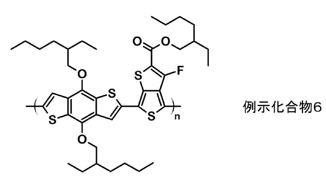
(実施例19)
<光電変換モジュールの作製>
実施例18の光電変換モジュールの作製において、長さLの最大値Lmax及び最小値Lminの差が1000nmになるように封止領域を形成した以外は実施例18と同様にして光電変換モジュールを作製した。
また、実施例1と同様に長さLの最大値Lmax及び最小値Lminの差の測定と、光電変換効率の維持率の算出と、を行った。結果を表1に示す。
(Example 19)
<Fabrication of photoelectric conversion module>
In the fabrication of the photoelectric conversion module of Example 18, the photoelectric conversion module was fabricated in the same manner as in Example 18, except that the sealing region was formed so that the difference between the maximum value Lmax and the minimum value Lmin of the length L was 1000 nm. was made.
Further, in the same manner as in Example 1, the difference between the maximum value Lmax and the minimum value Lmin of the length L was measured, and the photoelectric conversion efficiency maintenance rate was calculated. Table 1 shows the results.
(実施例20)
<光電変換モジュールの作製>
実施例3の光電変換モジュールの作製において、光電変換層塗工液Aを下記の光電変換層塗工液Gに変更した以外は実施例3と同様にして光電変換モジュールを作製した。
また、実施例1と同様に長さLの最大値Lmax及び最小値Lminの差の測定と、光電変換効率の維持率の算出と、を行った。結果を表1に示す。
(Example 20)
<Fabrication of photoelectric conversion module>
A photoelectric conversion module was produced in the same manner as in Example 3, except that the photoelectric conversion layer coating solution A was changed to the photoelectric conversion layer coating solution G below.
Further, in the same manner as in Example 1, the difference between the maximum value Lmax and the minimum value Lmin of the length L was measured, and the photoelectric conversion efficiency maintenance rate was calculated. Table 1 shows the results.
-光電変換層塗工液G-
下記に示す例示化合物7(数平均分子量(Mn)=1,806、最高被占軌道(HOMO)準位:5.20eV)15.5mgと、下記に示す例示化合物3の10mgを、クロロホルム1mLに溶解させ、光電変換層塗工液Gとした。
-Photoelectric conversion layer coating solution G-
Exemplified compound 7 shown below (number average molecular weight (Mn) = 1,806, highest occupied molecular orbital (HOMO) level: 5.20 eV) 15.5 mg and 10 mg of


(実施例21)
<光電変換モジュールの作製>
実施例20の光電変換モジュールの作製において、長さLの最大値Lmax及び最小値Lminの差が1000nmになるように封止領域を形成した以外は実施例20と同様にして光電変換モジュールを作製した。
また、実施例1と同様に長さLの最大値Lmax及び最小値Lminの差の測定と、光電変換効率の維持率の算出と、を行った。結果を表1に示す。
(Example 21)
<Fabrication of photoelectric conversion module>
The photoelectric conversion module of Example 20 was fabricated in the same manner as in Example 20, except that the sealing region was formed so that the difference between the maximum value Lmax and the minimum value Lmin of the length L was 1000 nm. was made.
Further, in the same manner as in Example 1, the difference between the maximum value Lmax and the minimum value Lmin of the length L was measured, and the photoelectric conversion efficiency maintenance rate was calculated. Table 1 shows the results.
(実施例22)
<光電変換モジュールの作製>
実施例3の光電変換モジュールの作製において、光電変換層塗工液Aを下記の光電変換層塗工液Hに変更した以外は実施例3と同様にして光電変換モジュールを作製した。
また、実施例1と同様に長さLの最大値Lmax及び最小値Lminの差の測定と、光電変換効率の維持率の算出と、を行った。結果を表1に示す。
(Example 22)
<Fabrication of photoelectric conversion module>
A photoelectric conversion module was produced in the same manner as in Example 3, except that the photoelectric conversion layer coating solution A was changed to the photoelectric conversion layer coating solution H below.
Further, in the same manner as in Example 1, the difference between the maximum value Lmax and the minimum value Lmin of the length L was measured, and the photoelectric conversion efficiency maintenance rate was calculated. Table 1 shows the results.
-光電変換層塗工液H-
下記に示す例示化合物8(数平均分子量(Mn)=1,886、最高被占軌道(HOMO)準位:5.00eV)16mgと、下記に示す例示化合物3の10mgを、クロロホルム1mLに溶解させ、光電変換層塗工液Hとした。
-Photoelectric conversion layer coating liquid H-
Exemplary compound 8 shown below (number average molecular weight (Mn) = 1,886, highest occupied molecular orbital (HOMO) level: 5.00 eV) 16 mg and 10 mg of

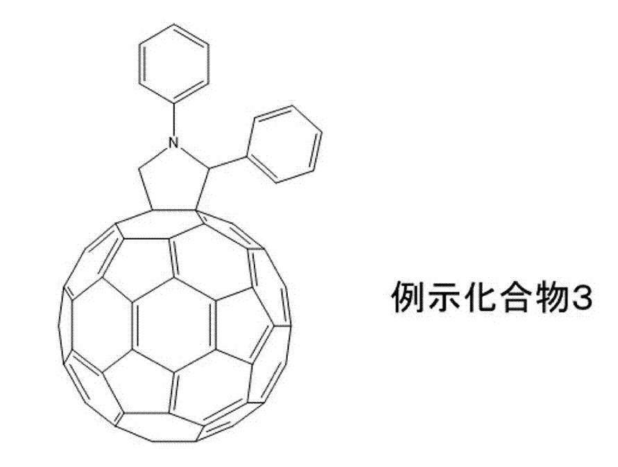
(実施例23)
<光電変換モジュールの作製>
実施例22の光電変換モジュールの作製において、長さLの最大値Lmax及び最小値Lminの差が1000nmになるように封止領域を形成した以外は実施例22と同様にして光電変換モジュールを作製した。
また、実施例1と同様に長さLの最大値Lmax及び最小値Lminの差の測定と、光電変換効率の維持率の算出と、を行った。結果を表1に示す。
(Example 23)
<Fabrication of photoelectric conversion module>
In the fabrication of the photoelectric conversion module of Example 22, the photoelectric conversion module was fabricated in the same manner as in Example 22, except that the sealing region was formed so that the difference between the maximum value Lmax and the minimum value Lmin of the length L was 1000 nm. was made.
Further, in the same manner as in Example 1, the difference between the maximum value Lmax and the minimum value Lmin of the length L was measured, and the photoelectric conversion efficiency maintenance rate was calculated. Table 1 shows the results.
(実施例24)
<光電変換モジュールの作製>
実施例3の光電変換モジュールの作製において、光電変換層塗工液Aを下記の光電変換層塗工液Iに変更した以外は実施例3と同様にして光電変換モジュールを作製した。
また、実施例1と同様に長さLの最大値Lmax及び最小値Lminの差の測定と、光電変換効率の維持率の算出と、を行った。結果を表1に示す。
(Example 24)
<Fabrication of photoelectric conversion module>
A photoelectric conversion module was produced in the same manner as in Example 3, except that the photoelectric conversion layer coating solution A was changed to the photoelectric conversion layer coating solution I below.
Further, in the same manner as in Example 1, the difference between the maximum value Lmax and the minimum value Lmin of the length L was measured, and the photoelectric conversion efficiency maintenance rate was calculated. Table 1 shows the results.
-光電変換層塗工液I-
P3HT(aldrich社製,数平均分子量(Mn)=54,000,最高被占軌道(HOMO)準位:5.00eV)10mgと、PC61BM(E100H,フロンティアカーボン社製)10mgを、クロロホルム1mLに溶解させ、光電変換層塗工液Gとした。
-Photoelectric conversion layer coating solution I-
10 mg of P3HT (manufactured by aldrich, number average molecular weight (Mn) = 54,000, highest occupied molecular orbital (HOMO) level: 5.00 eV) and 10 mg of PC61BM (E100H, manufactured by Frontier Carbon) were dissolved in 1 mL of chloroform. and a photoelectric conversion layer coating solution G was obtained.
(実施例25)
<光電変換モジュールの作製>
実施例24の光電変換モジュールの作製において、長さLの最大値Lmax及び最小値Lminの差が1000nmになるように封止領域を形成した以外は実施例24と同様にして光電変換モジュールを作製した。
また、実施例1と同様に長さLの最大値Lmax及び最小値Lminの差の測定と、光電変換効率の維持率の算出と、を行った。結果を表1に示す。
(Example 25)
<Fabrication of photoelectric conversion module>
In the fabrication of the photoelectric conversion module of Example 24, the photoelectric conversion module was fabricated in the same manner as in Example 24, except that the sealing region was formed so that the difference between the maximum value Lmax and the minimum value Lmin of the length L was 1000 nm. was made.
Further, in the same manner as in Example 1, the difference between the maximum value Lmax and the minimum value Lmin of the length L was measured, and the photoelectric conversion efficiency maintenance rate was calculated. Table 1 shows the results.
(実施例26)
<光電変換モジュールの作製>
実施例3の光電変換モジュールの作製において、第二の電子輸送層(中間層)を形成しなかった以外は実施例3と同様にして光電変換モジュールを作製した。
また、実施例1と同様に長さLの最大値Lmax及び最小値Lminの差の測定と、光電変換効率の維持率の算出と、を行った。結果を表1に示す。
(Example 26)
<Fabrication of photoelectric conversion module>
A photoelectric conversion module was fabricated in the same manner as in Example 3, except that the second electron transport layer (intermediate layer) was not formed.
Further, in the same manner as in Example 1, the difference between the maximum value Lmax and the minimum value Lmin of the length L was measured, and the photoelectric conversion efficiency maintenance rate was calculated. Table 1 shows the results.
(実施例27)
<光電変換モジュールの作製>
実施例26の光電変換モジュールの作製において、長さLの最大値Lmax及び最小値Lminの差が1000nmになるように封止領域を形成した以外は実施例26と同様にして光電変換モジュールを作製した。
また、実施例1と同様に長さLの最大値Lmax及び最小値Lminの差の測定と、光電変換効率の維持率の算出と、を行った。結果を表1に示す。
(Example 27)
<Fabrication of photoelectric conversion module>
In the fabrication of the photoelectric conversion module of Example 26, the photoelectric conversion module was fabricated in the same manner as in Example 26, except that the sealing region was formed so that the difference between the maximum value Lmax and the minimum value Lmin of the length L was 1000 nm. was made.
Further, in the same manner as in Example 1, the difference between the maximum value Lmax and the minimum value Lmin of the length L was measured, and the photoelectric conversion efficiency maintenance rate was calculated. Table 1 shows the results.
(実施例28)
<光電変換モジュールの作製>
実施例3の光電変換モジュールの作製において、光電変換層塗工液Aを下記の光電変換層塗工液Jに変更した以外は実施例3と同様にして光電変換モジュールを作製した。
また、実施例1と同様に長さLの最大値Lmax及び最小値Lminの差の測定と、光電変換効率の維持率の算出と、を行った。結果を表1に示す。
(Example 28)
<Fabrication of photoelectric conversion module>
A photoelectric conversion module was produced in the same manner as in Example 3, except that the photoelectric conversion layer coating solution A was changed to the photoelectric conversion layer coating solution J below.
Further, in the same manner as in Example 1, the difference between the maximum value Lmax and the minimum value Lmin of the length L was measured, and the photoelectric conversion efficiency maintenance rate was calculated. Table 1 shows the results.
-光電変換層塗工液J-
下記に示す例示化合物1(数平均分子量(Mn)=1,554、最高被占軌道(HOMO)準位:5.13eV)10mgと、下記に示す例示化合物9(ITIC-F、Merck社製)の10mgを、クロロホルム1mLに溶解させ、光電変換層塗工液Jとした。
-Photoelectric conversion layer coating solution J-
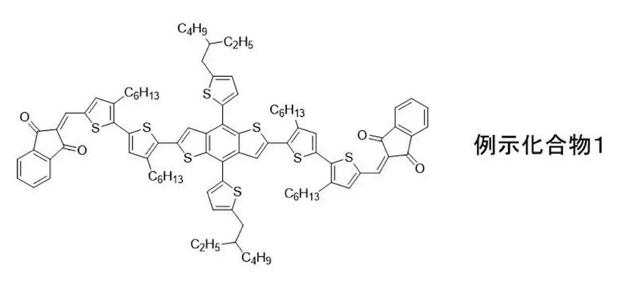

(実施例29)
<光電変換モジュールの作製>
実施例28の光電変換モジュールの作製において、長さLの最大値Lmax及び最小値Lminの差が1000nmになるように封止領域を形成した以外は実施例28と同様にして光電変換モジュールを作製した。
また、実施例1と同様に長さLの最大値Lmax及び最小値Lminの差の測定と、光電変換効率の維持率の算出と、を行った。結果を表1に示す。
(Example 29)
<Fabrication of photoelectric conversion module>
In the fabrication of the photoelectric conversion module of Example 28, the photoelectric conversion module was fabricated in the same manner as in Example 28, except that the sealing region was formed so that the difference between the maximum value Lmax and the minimum value Lmin of the length L was 1000 nm. was made.
Further, in the same manner as in Example 1, the difference between the maximum value Lmax and the minimum value Lmin of the length L was measured, and the photoelectric conversion efficiency maintenance rate was calculated. Table 1 shows the results.
(比較例1)
<光電変換モジュールの作製>
実施例1の光電変換モジュールの作製において、長さLの最大値Lmax及び最小値Lminの差が1050nmになるように封止領域を形成した以外は実施例1と同様にして光電変換モジュールを作製した。
また、実施例1と同様に長さLの最大値Lmax及び最小値Lminの差の測定と、光電変換効率の維持率の算出と、を行った。結果を表2に示す。
(Comparative example 1)
<Fabrication of photoelectric conversion module>
In the fabrication of the photoelectric conversion module of Example 1, the photoelectric conversion module was fabricated in the same manner as in Example 1, except that the sealing region was formed so that the difference between the maximum value Lmax and the minimum value Lmin of the length L was 1050 nm. was made.
Further, in the same manner as in Example 1, the difference between the maximum value Lmax and the minimum value Lmin of the length L was measured, and the photoelectric conversion efficiency maintenance rate was calculated. Table 2 shows the results.
(比較例2)
<光電変換モジュールの作製>
実施例1の光電変換モジュールの作製において、長さLの最大値Lmax及び最小値Lminの差が1100nmになるように封止領域を形成した以外は実施例1と同様にして光電変換モジュールを作製した。
また、実施例1と同様に長さLの最大値Lmax及び最小値Lminの差の測定と、光電変換効率の維持率の算出と、を行った。結果を表2に示す。
(Comparative example 2)
<Fabrication of photoelectric conversion module>
In the fabrication of the photoelectric conversion module of Example 1, the photoelectric conversion module was fabricated in the same manner as in Example 1, except that the sealing region was formed so that the difference between the maximum value Lmax and the minimum value Lmin of the length L was 1100 nm. was made.
Further, in the same manner as in Example 1, the difference between the maximum value Lmax and the minimum value Lmin of the length L was measured, and the photoelectric conversion efficiency maintenance rate was calculated. Table 2 shows the results.
(比較例3)
<光電変換モジュールの作製>
実施例1の光電変換モジュールの作製において、長さLの最大値Lmax及び最小値Lminの差が1300nmになるように封止領域を形成した以外は実施例1と同様にして光電変換モジュールを作製した。
また、実施例1と同様に長さLの最大値Lmax及び最小値Lminの差の測定と、光電変換効率の維持率の算出と、を行った。結果を表2に示す。
(Comparative Example 3)
<Fabrication of photoelectric conversion module>
In the fabrication of the photoelectric conversion module of Example 1, the photoelectric conversion module was fabricated in the same manner as in Example 1, except that the sealing region was formed so that the difference between the maximum value Lmax and the minimum value Lmin of the length L was 1300 nm. was made.
Further, in the same manner as in Example 1, the difference between the maximum value Lmax and the minimum value Lmin of the length L was measured, and the photoelectric conversion efficiency maintenance rate was calculated. Table 2 shows the results.
(比較例4)
<光電変換モジュールの作製>
比較例1の光電変換モジュールの作製において、封止部材を、エポキシ系樹脂の接着部材及びAl/PET積層ガスバリア部材が一体化して形成された封止部材(テサテープ株式会社製)に変更した以外は比較例1と同様にして光電変換モジュールを作製した。
また、実施例1と同様に長さLの最大値Lmax及び最小値Lminの差の測定と、光電変換効率の維持率の算出と、を行った。結果を表2に示す。
(Comparative Example 4)
<Fabrication of photoelectric conversion module>
In the fabrication of the photoelectric conversion module of Comparative Example 1, except that the sealing member was changed to a sealing member (manufactured by Tesa Tape Co., Ltd.) formed by integrating an epoxy-based resin adhesive member and an Al/PET laminated gas barrier member. A photoelectric conversion module was produced in the same manner as in Comparative Example 1.
Further, in the same manner as in Example 1, the difference between the maximum value Lmax and the minimum value Lmin of the length L was measured, and the photoelectric conversion efficiency maintenance rate was calculated. Table 2 shows the results.
(比較例5)
<光電変換モジュールの作製>
比較例1の光電変換モジュールの作製において、封止部材を、シリコーン系樹脂の接着部材及びAl/PET積層ガスバリア部材が一体化して形成された封止部材(テサテープ株式会社製)に変更した以外は比較例1と同様にして光電変換モジュールを作製した。
また、実施例1と同様に長さLの最大値Lmax及び最小値Lminの差の測定と、光電変換効率の維持率の算出と、を行った。結果を表2に示す。
(Comparative Example 5)
<Fabrication of photoelectric conversion module>
In the fabrication of the photoelectric conversion module of Comparative Example 1, except that the sealing member was changed to a sealing member (manufactured by Tesa Tape Co., Ltd.) formed by integrating a silicone-based resin adhesive member and an Al/PET laminated gas barrier member. A photoelectric conversion module was produced in the same manner as in Comparative Example 1.
Further, in the same manner as in Example 1, the difference between the maximum value Lmax and the minimum value Lmin of the length L was measured, and the photoelectric conversion efficiency maintenance rate was calculated. Table 2 shows the results.
(比較例6)
<光電変換モジュールの作製>
比較例1の光電変換モジュールの作製において、封止部材を、アクリル系樹脂の接着部材及びAl/PET積層ガスバリア部材が一体化して形成された封止部材(テサテープ株式会社製)に変更した以外は比較例1と同様にして光電変換モジュールを作製した。
また、実施例1と同様に長さLの最大値Lmax及び最小値Lminの差の測定と、光電変換効率の維持率の算出と、を行った。結果を表2に示す。
(Comparative Example 6)
<Fabrication of photoelectric conversion module>
In the fabrication of the photoelectric conversion module of Comparative Example 1, except that the sealing member was changed to a sealing member (manufactured by Tesa Tape Co., Ltd.) formed by integrating an acrylic resin adhesive member and an Al/PET laminated gas barrier member. A photoelectric conversion module was produced in the same manner as in Comparative Example 1.
Further, in the same manner as in Example 1, the difference between the maximum value Lmax and the minimum value Lmin of the length L was measured, and the photoelectric conversion efficiency maintenance rate was calculated. Table 2 shows the results.
(比較例7)
<光電変換モジュールの作製>
実施例10の光電変換モジュールの作製において、長さLの最大値Lmax及び最小値Lminの差が1050nmになるように封止領域を形成した以外は実施例10と同様にして光電変換モジュールを作製した。
また、実施例1と同様に長さLの最大値Lmax及び最小値Lminの差の測定と、光電変換効率の維持率の算出と、を行った。結果を表2に示す。
(Comparative Example 7)
<Fabrication of photoelectric conversion module>
The photoelectric conversion module of Example 10 was fabricated in the same manner as in Example 10, except that the sealing region was formed so that the difference between the maximum value L max and the minimum value L min of the length L was 1050 nm. was made.
Further, in the same manner as in Example 1, the difference between the maximum value Lmax and the minimum value Lmin of the length L was measured, and the photoelectric conversion efficiency maintenance rate was calculated. Table 2 shows the results.
(比較例8)
<光電変換モジュールの作製>
実施例12の光電変換モジュールの作製において、長さLの最大値Lmax及び最小値Lminの差が1050nmになるように封止領域を形成した以外は実施例12と同様にして光電変換モジュールを作製した。
また、実施例1と同様に長さLの最大値Lmax及び最小値Lminの差の測定と、光電変換効率の維持率の算出と、を行った。結果を表2に示す。
(Comparative Example 8)
<Fabrication of photoelectric conversion module>
The photoelectric conversion module of Example 12 was fabricated in the same manner as in Example 12, except that the sealing region was formed such that the difference between the maximum value L max and the minimum value L min of the length L was 1050 nm. was made.
Further, in the same manner as in Example 1, the difference between the maximum value Lmax and the minimum value Lmin of the length L was measured, and the photoelectric conversion efficiency maintenance rate was calculated. Table 2 shows the results.
(比較例9)
<光電変換モジュールの作製>
実施例14の光電変換モジュールの作製において、長さLの最大値Lmax及び最小値Lminの差が1050nmになるように封止領域を形成した以外は実施例14と同様にして光電変換モジュールを作製した。
また、実施例1と同様に長さLの最大値Lmax及び最小値Lminの差の測定と、光電変換効率の維持率の算出と、を行った。結果を表2に示す。
(Comparative Example 9)
<Fabrication of photoelectric conversion module>
The photoelectric conversion module of Example 14 was fabricated in the same manner as in Example 14, except that the sealing region was formed so that the difference between the maximum value L max and the minimum value L min of the length L was 1050 nm. was made.
Further, in the same manner as in Example 1, the difference between the maximum value Lmax and the minimum value Lmin of the length L was measured, and the photoelectric conversion efficiency maintenance rate was calculated. Table 2 shows the results.
(比較例10)
<光電変換モジュールの作製>
実施例16の光電変換モジュールの作製において、長さLの最大値Lmax及び最小値Lminの差が1050nmになるように封止領域を形成した以外は実施例16と同様にして光電変換モジュールを作製した。
また、実施例1と同様に長さLの最大値Lmax及び最小値Lminの差の測定と、光電変換効率の維持率の算出と、を行った。結果を表2に示す。
(Comparative Example 10)
<Fabrication of photoelectric conversion module>
The photoelectric conversion module of Example 16 was fabricated in the same manner as in Example 16, except that the sealing region was formed so that the difference between the maximum value L max and the minimum value L min of the length L was 1050 nm. was made.
Further, in the same manner as in Example 1, the difference between the maximum value Lmax and the minimum value Lmin of the length L was measured, and the photoelectric conversion efficiency maintenance rate was calculated. Table 2 shows the results.
(比較例11)
<光電変換モジュールの作製>
実施例18の光電変換モジュールの作製において、長さLの最大値Lmax及び最小値Lminの差が1050nmになるように封止領域を形成した以外は実施例18と同様にして光電変換モジュールを作製した。
また、実施例1と同様に長さLの最大値Lmax及び最小値Lminの差の測定と、光電変換効率の維持率の算出と、を行った。結果を表2に示す。
(Comparative Example 11)
<Fabrication of photoelectric conversion module>
The photoelectric conversion module of Example 18 was fabricated in the same manner as in Example 18, except that the sealing region was formed so that the difference between the maximum value L max and the minimum value L min of the length L was 1050 nm. was made.
Further, in the same manner as in Example 1, the difference between the maximum value Lmax and the minimum value Lmin of the length L was measured, and the photoelectric conversion efficiency maintenance rate was calculated. Table 2 shows the results.
(比較例12)
<光電変換モジュールの作製>
実施例20の光電変換モジュールの作製において、長さLの最大値Lmax及び最小値Lminの差が1050nmになるように封止領域を形成した以外は実施例20と同様にして光電変換モジュールを作製した。
また、実施例1と同様に長さLの最大値Lmax及び最小値Lminの差の測定と、光電変換効率の維持率の算出と、を行った。結果を表2に示す。
(Comparative Example 12)
<Fabrication of photoelectric conversion module>
In the fabrication of the photoelectric conversion module of Example 20, the photoelectric conversion module was fabricated in the same manner as in Example 20, except that the sealing region was formed so that the difference between the maximum value Lmax and the minimum value Lmin of the length L was 1050 nm. was made.
Further, in the same manner as in Example 1, the difference between the maximum value Lmax and the minimum value Lmin of the length L was measured, and the photoelectric conversion efficiency maintenance rate was calculated. Table 2 shows the results.
(比較例13)
<光電変換モジュールの作製>
実施例22の光電変換モジュールの作製において、長さLの最大値Lmax及び最小値Lminの差が1050nmになるように封止領域を形成した以外は実施例22と同様にして光電変換モジュールを作製した。
また、実施例1と同様に長さLの最大値Lmax及び最小値Lminの差の測定と、光電変換効率の維持率の算出と、を行った。結果を表2に示す。
(Comparative Example 13)
<Fabrication of photoelectric conversion module>
The photoelectric conversion module of Example 22 was fabricated in the same manner as in Example 22, except that the sealing region was formed such that the difference between the maximum value L max and the minimum value L min of the length L was 1050 nm. was made.
Further, in the same manner as in Example 1, the difference between the maximum value Lmax and the minimum value Lmin of the length L was measured, and the photoelectric conversion efficiency maintenance rate was calculated. Table 2 shows the results.
(比較例14)
<光電変換モジュールの作製>
実施例24の光電変換モジュールの作製において、長さLの最大値Lmax及び最小値Lminの差が1050nmになるように封止領域を形成した以外は実施例24と同様にして光電変換モジュールを作製した。
また、実施例1と同様に長さLの最大値Lmax及び最小値Lminの差の測定と、光電変換効率の維持率の算出と、を行った。結果を表2に示す。
(Comparative Example 14)
<Fabrication of photoelectric conversion module>
In the fabrication of the photoelectric conversion module of Example 24, the photoelectric conversion module was fabricated in the same manner as in Example 24, except that the sealing region was formed so that the difference between the maximum value Lmax and the minimum value Lmin of the length L was 1050 nm. was made.
Further, in the same manner as in Example 1, the difference between the maximum value Lmax and the minimum value Lmin of the length L was measured, and the photoelectric conversion efficiency maintenance rate was calculated. Table 2 shows the results.
(比較例15)
<光電変換モジュールの作製>
実施例26の光電変換モジュールの作製において、長さLの最大値Lmax及び最小値Lminの差が1050nmになるように封止領域を形成した以外は実施例26と同様にして光電変換モジュールを作製した。
また、実施例1と同様に長さLの最大値Lmax及び最小値Lminの差の測定と、光電変換効率の維持率の算出と、を行った。結果を表2に示す。
(Comparative Example 15)
<Fabrication of photoelectric conversion module>
In the fabrication of the photoelectric conversion module of Example 26, the photoelectric conversion module was fabricated in the same manner as in Example 26, except that the sealing region was formed so that the difference between the maximum value Lmax and the minimum value Lmin of the length L was 1050 nm. was made.
Further, in the same manner as in Example 1, the difference between the maximum value Lmax and the minimum value Lmin of the length L was measured, and the photoelectric conversion efficiency maintenance rate was calculated. Table 2 shows the results.
(比較例16)
<光電変換モジュールの作製>
実施例28の光電変換モジュールの作製において、長さLの最大値Lmax及び最小値Lminの差が1050nmになるように封止領域を形成した以外は実施例28と同様にして光電変換モジュールを作製した。
また、実施例1と同様に長さLの最大値Lmax及び最小値Lminの差の測定と、光電変換効率の維持率の算出と、を行った。結果を表2に示す。
(Comparative Example 16)
<Fabrication of photoelectric conversion module>
In the fabrication of the photoelectric conversion module of Example 28, the photoelectric conversion module was fabricated in the same manner as in Example 28, except that the sealing region was formed so that the difference between the maximum value Lmax and the minimum value Lmin of the length L was 1050 nm. was made.
Further, in the same manner as in Example 1, the difference between the maximum value Lmax and the minimum value Lmin of the length L was measured, and the photoelectric conversion efficiency maintenance rate was calculated. Table 2 shows the results.


表1及び表2の結果から、本開示の光電変換素子は、長さLの最大値Lmax及び最小値Lminの差が1000nm以下であることで、高温高湿環境下に長時間置かれたとしても光電変換効率の低下が抑制されることが分かった。 From the results of Tables 1 and 2, the photoelectric conversion element of the present disclosure has a difference of 1000 nm or less between the maximum value L max and the minimum value L min of the length L, so that it can be placed in a high temperature and high humidity environment for a long time. It was found that the decrease in the photoelectric conversion efficiency was suppressed even if the
1 光電変換素子
2 光電変換領域
3 封止領域
4 その他部材
11 UVカット層
12 基材
13 第一の電極
14 第一の電子輸送層
15 第二の電子輸送層(中間層)
16 光電変換層
17 正孔輸送層
18 第二の電極
19 表面保護層
20 封止部材
21 接着部材
22 ガスバリア部材
23 付着物
30 接着領域
31 接着領域を有さない面
REFERENCE SIGNS
REFERENCE SIGNS
Claims (14)
前記第一の電極及び前記第二の電極から選ばれる一方の電極と光電変換層とを内包し、且つ前記第一の電極及び前記第二の電極から選ばれる他方の電極における接着領域と接着する封止部材を有し、
前記光電変換素子の積層方向を含む断面において、前記他方の電極における前記接着領域を有さない面から前記接着領域と接着している前記封止部材までの積層方向における長さLの最大値及び最小値の差は、1000nm以下であることを特徴とする光電変換素子。 A photoelectric conversion element sequentially having a first electrode, a photoelectric conversion layer, and a second electrode,
Including one electrode selected from the first electrode and the second electrode and a photoelectric conversion layer, and bonding with the bonding region in the other electrode selected from the first electrode and the second electrode having a sealing member;
In a cross section including the stacking direction of the photoelectric conversion element, the maximum value of the length L in the stacking direction from the surface of the other electrode that does not have the bonding region to the sealing member that is bonded to the bonding region, and A photoelectric conversion element, wherein the minimum value difference is 1000 nm or less.
前記接着部材は、エポキシ系樹脂及びポリオレフィン系樹脂からなる群より選ばれる少なくとも1つを含有する請求項1から3のいずれか一項に記載の光電変換素子。 The sealing member has an adhesive member for adhering to the other electrode,
The photoelectric conversion element according to any one of claims 1 to 3, wherein the adhesive member contains at least one selected from the group consisting of epoxy resin and polyolefin resin.
前記基材は、ガスバリア性を有する請求項1から5のいずれか一項に記載の光電変換素子。 Further, a base material is provided on the side of the other electrode that does not have the adhesive region,
The photoelectric conversion element according to any one of claims 1 to 5, wherein the substrate has gas barrier properties.


前記第一の電子輸送層は、金属酸化物の粒子を含有し、
前記第二の電子輸送層は、下記一般式(4)で表されるアミン化合物を含有する請求項7に記載の光電変換素子。
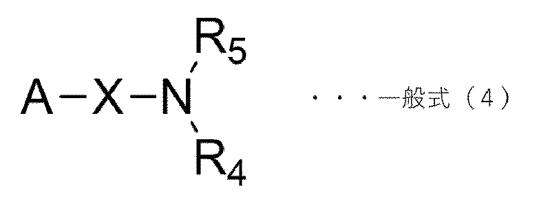
The first electron-transporting layer contains metal oxide particles,
8. The photoelectric conversion device according to claim 7, wherein the second electron transport layer contains an amine compound represented by the following general formula (4).
Priority Applications (2)
| Application Number | Priority Date | Filing Date | Title |
|---|---|---|---|
| JP2021044329A JP2022143679A (en) | 2021-03-18 | 2021-03-18 | Photoelectric conversion elements, electronic devices, and power supply modules |
| EP22160519.9A EP4064376B1 (en) | 2021-03-18 | 2022-03-07 | Photoelectric conversion element |
Applications Claiming Priority (1)
| Application Number | Priority Date | Filing Date | Title |
|---|---|---|---|
| JP2021044329A JP2022143679A (en) | 2021-03-18 | 2021-03-18 | Photoelectric conversion elements, electronic devices, and power supply modules |
Publications (1)
| Publication Number | Publication Date |
|---|---|
| JP2022143679A true JP2022143679A (en) | 2022-10-03 |
Family
ID=80684101
Family Applications (1)
| Application Number | Title | Priority Date | Filing Date |
|---|---|---|---|
| JP2021044329A Pending JP2022143679A (en) | 2021-03-18 | 2021-03-18 | Photoelectric conversion elements, electronic devices, and power supply modules |
Country Status (2)
| Country | Link |
|---|---|
| EP (1) | EP4064376B1 (en) |
| JP (1) | JP2022143679A (en) |
Families Citing this family (2)
| Publication number | Priority date | Publication date | Assignee | Title |
|---|---|---|---|---|
| MX2023009682A (en) | 2021-02-19 | 2023-10-30 | Sudo Biosciences Ltd | Tyk2 inhibitors and uses thereof. |
| IL305165A (en) | 2021-02-19 | 2023-10-01 | Sudo Biosciences Ltd | TYK2 inhibitors and their uses |
Citations (7)
| Publication number | Priority date | Publication date | Assignee | Title |
|---|---|---|---|---|
| JP2003092417A (en) * | 2001-09-18 | 2003-03-28 | Seiko Epson Corp | Photoelectric conversion element |
| WO2010106853A1 (en) * | 2009-03-16 | 2010-09-23 | コニカミノルタホールディングス株式会社 | Organic electronic panel and method for manufacturing organic electronic panel |
| JP2010287800A (en) * | 2009-06-12 | 2010-12-24 | Tokki Corp | Organic device manufacturing apparatus and organic device manufacturing method |
| JP2012054494A (en) * | 2010-09-03 | 2012-03-15 | Dainippon Printing Co Ltd | Solar cell and solar cell module |
| WO2015022922A1 (en) * | 2013-08-14 | 2015-02-19 | Jx日鉱日石エネルギー株式会社 | Light emitting element and method for manufacturing light emitting element |
| JP2018152516A (en) * | 2017-03-14 | 2018-09-27 | 株式会社豊田中央研究所 | SOLAR CELL, SOLAR CELL MODULE, AND SOLAR CELL MANUFACTURING METHOD |
| JP2020025068A (en) * | 2018-07-31 | 2020-02-13 | 株式会社リコー | Photoelectric conversion element, photoelectric conversion element module, organic thin-film solar cell, electronic device, and power supply module |
Family Cites Families (3)
| Publication number | Priority date | Publication date | Assignee | Title |
|---|---|---|---|---|
| DE102004063133A1 (en) * | 2004-12-22 | 2006-07-13 | Schott Ag | Organic electrical or electronic component with increased lifetime |
| JP2014220333A (en) | 2013-05-07 | 2014-11-20 | Jx日鉱日石エネルギー株式会社 | Method of manufacturing photoelectric conversion element and photoelectric conversion element |
| CN106876586A (en) * | 2015-11-24 | 2017-06-20 | 松下电器产业株式会社 | Solar Cell |
-
2021
- 2021-03-18 JP JP2021044329A patent/JP2022143679A/en active Pending
-
2022
- 2022-03-07 EP EP22160519.9A patent/EP4064376B1/en active Active
Patent Citations (7)
| Publication number | Priority date | Publication date | Assignee | Title |
|---|---|---|---|---|
| JP2003092417A (en) * | 2001-09-18 | 2003-03-28 | Seiko Epson Corp | Photoelectric conversion element |
| WO2010106853A1 (en) * | 2009-03-16 | 2010-09-23 | コニカミノルタホールディングス株式会社 | Organic electronic panel and method for manufacturing organic electronic panel |
| JP2010287800A (en) * | 2009-06-12 | 2010-12-24 | Tokki Corp | Organic device manufacturing apparatus and organic device manufacturing method |
| JP2012054494A (en) * | 2010-09-03 | 2012-03-15 | Dainippon Printing Co Ltd | Solar cell and solar cell module |
| WO2015022922A1 (en) * | 2013-08-14 | 2015-02-19 | Jx日鉱日石エネルギー株式会社 | Light emitting element and method for manufacturing light emitting element |
| JP2018152516A (en) * | 2017-03-14 | 2018-09-27 | 株式会社豊田中央研究所 | SOLAR CELL, SOLAR CELL MODULE, AND SOLAR CELL MANUFACTURING METHOD |
| JP2020025068A (en) * | 2018-07-31 | 2020-02-13 | 株式会社リコー | Photoelectric conversion element, photoelectric conversion element module, organic thin-film solar cell, electronic device, and power supply module |
Also Published As
| Publication number | Publication date |
|---|---|
| EP4064376B1 (en) | 2024-05-01 |
| EP4064376A1 (en) | 2022-09-28 |
Similar Documents
| Publication | Publication Date | Title |
|---|---|---|
| WO2020026752A1 (en) | Photoelectric conversion element, photoelectric conversion element module, organic thin-film solar cell, electronic apparatus, and power supply module | |
| JP6880726B2 (en) | Photoelectric conversion element | |
| JP2021118190A (en) | Photoelectric conversion element, photoelectric conversion element module, electronic device, and power supply module | |
| EP4064376B1 (en) | Photoelectric conversion element | |
| EP4006979B1 (en) | Photoelectric conversion module, electronic device, and power supply module | |
| US20230232642A1 (en) | Photoelectric conversion element, photoelectric conversion element module, electronic device, power supply module, and method for producing photoelectric conversion element | |
| EP4122027B1 (en) | Photoelectric conversion element, photoelectric conversion module, electronic device, and power supply module | |
| JP7738819B2 (en) | Photoelectric conversion element, photoelectric conversion module, electronic device, and power supply module | |
| US20220173263A1 (en) | Photoelectric conversion module, electronic device, and power supply module | |
| JP2023056085A (en) | Photoelectric conversion elements, electronic devices, and power supply modules | |
| JP7677033B2 (en) | Photoelectric conversion element, electronic device, and power supply module |
Legal Events
| Date | Code | Title | Description |
|---|---|---|---|
| RD03 | Notification of appointment of power of attorney |
Free format text: JAPANESE INTERMEDIATE CODE: A7423 Effective date: 20231117 |
|
| A621 | Written request for application examination |
Free format text: JAPANESE INTERMEDIATE CODE: A621 Effective date: 20240119 |
|
| A977 | Report on retrieval |
Free format text: JAPANESE INTERMEDIATE CODE: A971007 Effective date: 20241113 |
|
| A131 | Notification of reasons for refusal |
Free format text: JAPANESE INTERMEDIATE CODE: A131 Effective date: 20241118 |
|
| A02 | Decision of refusal |
Free format text: JAPANESE INTERMEDIATE CODE: A02 Effective date: 20250409 |