JP2022134875A - Ringing suppression circuit - Google Patents
Ringing suppression circuit Download PDFInfo
- Publication number
- JP2022134875A JP2022134875A JP2021034348A JP2021034348A JP2022134875A JP 2022134875 A JP2022134875 A JP 2022134875A JP 2021034348 A JP2021034348 A JP 2021034348A JP 2021034348 A JP2021034348 A JP 2021034348A JP 2022134875 A JP2022134875 A JP 2022134875A
- Authority
- JP
- Japan
- Prior art keywords
- circuit
- control signal
- period
- ringing
- ringing suppression
- Prior art date
- Legal status (The legal status is an assumption and is not a legal conclusion. Google has not performed a legal analysis and makes no representation as to the accuracy of the status listed.)
- Pending
Links
Images


Classifications
-
- H—ELECTRICITY
- H04—ELECTRIC COMMUNICATION TECHNIQUE
- H04B—TRANSMISSION
- H04B3/00—Line transmission systems
- H04B3/02—Details
- H04B3/20—Reducing echo effects or singing; Opening or closing transmitting path; Conditioning for transmission in one direction or the other
-
- H—ELECTRICITY
- H04—ELECTRIC COMMUNICATION TECHNIQUE
- H04L—TRANSMISSION OF DIGITAL INFORMATION, e.g. TELEGRAPHIC COMMUNICATION
- H04L12/00—Data switching networks
- H04L12/28—Data switching networks characterised by path configuration, e.g. LAN [Local Area Networks] or WAN [Wide Area Networks]
- H04L12/40—Bus networks
- H04L2012/40208—Bus networks characterized by the use of a particular bus standard
- H04L2012/40215—Controller Area Network CAN
-
- H—ELECTRICITY
- H04—ELECTRIC COMMUNICATION TECHNIQUE
- H04L—TRANSMISSION OF DIGITAL INFORMATION, e.g. TELEGRAPHIC COMMUNICATION
- H04L12/00—Data switching networks
- H04L12/28—Data switching networks characterised by path configuration, e.g. LAN [Local Area Networks] or WAN [Wide Area Networks]
- H04L12/40—Bus networks
- H04L2012/40267—Bus for use in transportation systems
- H04L2012/40273—Bus for use in transportation systems the transportation system being a vehicle
Landscapes
- Engineering & Computer Science (AREA)
- Computer Networks & Wireless Communication (AREA)
- Signal Processing (AREA)
- Dc Digital Transmission (AREA)
- Electronic Switches (AREA)
- Logic Circuits (AREA)
Abstract
Description
本発明の実施形態は、リンギング抑制回路に関する。 Embodiments of the present invention relate to ringing suppression circuits.
従来、車載ネットワークとして、CAN(Controller Area Network)が採用されている。CANは、バス(CANバス)のバスラインに引き込み線を介してノード(CANノード)を接続するライン型のネットワークである。CANにおいては、バスラインに引き込み線を追加接続することで、CANノードの追加を簡単に行うことができる。 Conventionally, a CAN (Controller Area Network) has been adopted as an in-vehicle network. CAN is a line-type network in which nodes (CAN nodes) are connected to bus lines of a bus (CAN bus) via drop lines. In CAN, additional CAN nodes can be easily added by additionally connecting lead-in lines to bus lines.
CANでは、通信品質を向上させるために、CANバスの末端に終端抵抗を配置する。しかしながら、CANバスに任意のCANノードを追加可能であることから、伝送線路のインピーダンスは理想状態であるとは限らず、信号伝送の際にリンギングが生じることがあるという課題がある。 In CAN, a terminating resistor is placed at the end of the CAN bus in order to improve communication quality. However, since any CAN node can be added to the CAN bus, the impedance of the transmission line is not necessarily in an ideal state, and ringing may occur during signal transmission.
実施形態は、CANバスに対する終端器の接続又は非接続を制御することによりリンギングを抑制することができるリンギング抑制回路を提供することを目的とする。 An object of the embodiment is to provide a ringing suppression circuit capable of suppressing ringing by controlling connection or disconnection of a terminator to a CAN bus.
実施形態のリンギング抑制回路は、終端器と、第1及び第2のバスライン相互間に前記終端器を接続するためのスイッチング素子と、前記第1及び第2のバスラインにより伝送された信号を受信する受信回路から前記信号の受信結果が与えられ、前記受信結果に基づいて前記スイッチング素子を制御するための制御信号を生成する制御信号生成回路と、を具備する。 A ringing suppression circuit according to an embodiment includes a terminator, a switching element for connecting the terminator between first and second bus lines, and a signal transmitted by the first and second bus lines. a control signal generation circuit that receives a reception result of the signal from a reception circuit that receives the signal and generates a control signal for controlling the switching element based on the reception result.
以下、図面を参照して本発明の実施の形態について詳細に説明する。 BEST MODE FOR CARRYING OUT THE INVENTION Hereinafter, embodiments of the present invention will be described in detail with reference to the drawings.
(第1の実施の形態)
図1は本発明の第1の実施の形態に係るリンギング抑制回路を示すブロック図である。本実施の形態においては、受信回路の出力を利用して、ドミナントからリセッシブへの変化を検出し、検出タイミングから所定期間だけCANバスのバスラインに終端器を接続可能とすることにより、リンギングを抑制して、安定した通信を可能にするものである。
(First embodiment)
FIG. 1 is a block diagram showing a ringing suppression circuit according to a first embodiment of the invention. In the present embodiment, the output of the receiving circuit is used to detect the change from dominant to recessive, and a terminator can be connected to the bus line of the CAN bus for a predetermined period from the detection timing, thereby suppressing ringing. It suppresses it and enables stable communication.
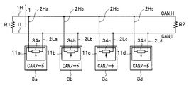
図2はCANバスのトポロジーを示す説明図である。図1は図2中の1つのCANノードに対して設けられるリンギング抑制回路の具体的な構成の一例を示している。また、図3はCANノードの比較例を採用したCANバスのトポロジーを示す説明図である。なお、図2及び図3において、同一の構成要素には同一符号を付して、重複する説明は省略するものとする。 FIG. 2 is an explanatory diagram showing the topology of the CAN bus. FIG. 1 shows an example of a specific configuration of a ringing suppression circuit provided for one CAN node in FIG. FIG. 3 is an explanatory diagram showing the topology of a CAN bus employing a comparative example of CAN nodes. In addition, in FIG.2 and FIG.3, the same code|symbol shall be attached|subjected to the same component, and the overlapping description shall be abbreviate|omitted.
図2に示すように、CANバス1は、CAN_Hライン1H及びCAH_Lライン1Lの2本のバスラインを有し、CAN_Hライン1H及びCAH_Lライン1Lによって差動信号を伝送する。CANバス1には、引き込み線2Ha,2La、引き込み線2Hb,2Lb、引き込み線2Hc,2Lc、引き込み線2Hd,2Ldをそれぞれ介してCANノード3a~3dが接続される。なお、引き込み線2Ha~2Hdを区別する必要がない場合には代表して引き込み線2Hといい、引き込み線2La~2Ldを区別する必要がない場合には代表して引き込み線2Lといい、引き込み線2Ha~2Hd,2La~2Ldを区別する必要がない場合には代表して引き込み線2という。また、CANノード3a~3dを区別する必要がない場合には代表してCANノード3という。
As shown in FIG. 2, the
CANバス1の一方端及び他方端には、CAN_Hライン1HとCAH_Lライン1Lとの間に終端抵抗R1,R2がそれぞれ接続される。
Termination resistors R1 and R2 are connected to one end and the other end of the
図1に示すように、CANノード3は、送信回路31と受信回路32とを有する。送信回路31は、引き込み線2Hを介してCAN_Hライン1Hに接続され、引き込み線2Lを介してCAH_Lライン1Lに接続される。また、同様に、受信回路32は、引き込み線2Hを介してCAN_Hライン1Hに接続され、引き込み線2Lを介してCAH_Lライン1Lに接続される。
As shown in FIG. 1, the CAN node 3 has a
CANノード3の送信回路31は、送信すべきデータをCANプロトコルに対応する送信データに変換した後、送信データの各ビットの値に応じて引き込み線2H,2Lを駆動することで信号の伝送を行う。送信回路31は、送信データの論理値"0"(ドミナント)を伝送する場合には、CAN_Hライン1H,1L間に所定の電圧差を生じさせ、送信データの論理値"1"(リセッシブ)を伝送する場合には、CAN_Hライン1H,1Lを同電圧とする。
The
例えば、送信回路31は、引き込み線2H,2Lを介してCAN_Hライン1H,1Lのいずれにも中点電圧を印加する信号経路を有し、この信号経路を用いて、リセッシブ時にはCAN_Hライン1H,1Lを同電圧とする。また、送信回路31は、引き込み線2Hを介してCAN_Hライン1Hに電流を供給し、引き込み線2Lを介してCAH_Lライン1Lから電流を引き抜く信号経路を有し、この信号経路を用いて、ドミナント時にはCAN_Hライン1H,1L間に所定の電圧を発生させる。
For example, the
受信回路32は、CANバス1を介して伝送された信号を受信して受信結果を出力する。例えば、受信回路32は、引き込み線2H,2Lを介してCAN_Hライン1H,1L間の電圧差を検出し、この電圧差が所定の閾値以下である場合にはリセッシブの伝送期間であると判定し、この電圧差が所定の閾値を超えた場合にはドミナントの伝送期間であると判定する。受信回路32は、リセッシブ期間とドミナント期間にそれぞれ対応するレベルの信号を受信結果として出力する。
The
(リンギング)
CANにおいては、上述したように、CANノード3をCANバス1に任意に接続可能であることから、データ送信時にインピーダンス不整合による反射が生じ、リンギングが発生する。ところで、リセッシブ時に中点電圧を印加する送信回路31内の信号経路のインピーダンスは、終端抵抗R1,R2の抵抗値に比べて極めて大きい。また、ドミナント時に電流を流す送信回路31内の信号経路のインピーダンスは、終端抵抗R1,R2と同様に比較的小さい。このため、リセッシブからドミナントへの移行時におけるリンギングのレベルは比較的小さく、ドミナントからリセッシブへの移行時におけるリンギングのレベルは比較的大きい。
(ringing)
In CAN, as described above, since the CAN node 3 can be arbitrarily connected to the
図4は図3に示す比較例のCANノードを採用した場合におけるリンギングの影響を説明するための波形図である。 FIG. 4 is a waveform diagram for explaining the influence of ringing when the CAN node of the comparative example shown in FIG. 3 is adopted.
図3に示す比較例のCANノード3Ra~3Rd(以下、これらを区別する必要がない場合には、代表してCANノード3Rという)は、図1の送信回路31及び受信回路32と同様の構成を有する。CANノード3R内の送信回路31において、図4に示す送信信号TXDを送信するものとする。即ち、この場合には、送信回路31は、リセッシブ期間においてCAN_Hライン1H,1Lをいずれも中点電圧とし、ドミナント期間においてCAN_Hライン1H,1L間に所定の電圧差を発生させる。
CAN nodes 3Ra to 3Rd of the comparative example shown in FIG. 3 (hereinafter referred to as CAN node 3R representatively when there is no need to distinguish between them) have the same configuration as the transmitting
即ち、CAN_Hライン1Hに流れるバス信号CAN_H(図4の実線)は、リセッシブ期間に中点電圧となり、ドミナント期間に中点電圧よりも高い電圧となる。また、CAN_Lライン1Lに流れるバス信号CAN_L(図4の細線)は、リセッシブ期間に中点電圧となり、ドミナント期間に中点電圧よりも低い電圧となる。
CANノード3R内の受信回路32は、引き込み線2Hに発生する電圧と、引き込み線2Lに発生する電圧との差電圧を求める。図4に示すように、差電圧(CAN_H-CAN_L)は、リセッシブ期間に0Vとなり、ドミナント期間には、図示しない所定の閾値を超える電圧レベルとなる。
That is, the bus signal CAN_H (the solid line in FIG. 4) flowing through the
A
しかしながら、上述したように、ドミナントからリセッシブへの移行時において比較的大きなレベルのリンギングが発生する結果、このリンギングによってドミナント期間からリセッシブ期間への移行直後において差電圧が図示しない所定の閾値を超える電圧となってしまう。CANノード3Rの受信回路32は、差電圧を所定の閾値と比較することで、ドミナント期間であるかリセッシブ期間であるかを判定する。即ち、図4の例では、CANノード3Rの受信回路32は、ドミナント期間においてドミナントを検出するだけでなく、ドミナント期間直後のリセッシブ期間においてもリンギングの影響によりドミナントを誤検出してしまう。
However, as described above, a relatively large level of ringing occurs at the transition from dominant to recessive, and as a result of this ringing, the difference voltage exceeds a predetermined threshold (not shown) immediately after the transition from the dominant period to the recessive period. becomes. The
なお、CANバス1において、終端抵抗R1,R2近傍のCANノード3Rにおいては比較的リンギングのレベルは小さく、終端抵抗R1,R2から離れた距離のCANノード3R程、リンギングのレベルは大きくなる。
In the
(構成)
そこで、本実施の形態においては、図2に示すように、ドミナントからリセッシブへの移行の検知結果に基づいて、リンギングを抑制するためのリンギング抑制回路11a~11d(以下、これらを区別する必要がない場合には、リンギング抑制回路11という)が各CANノード3a~3dにそれぞれ対応して設けられる。リンギング抑制回路11a~11dは相互に同一構成であり、リンギング抑制回路11a~11dには、リンギング抑制器34a~34d(以下、これらを区別する必要がない場合には、代表してリンギング抑制器34という)が設けられている。図1に示すように、リンギング抑制回路11は、リンギング抑制器34と各CANノード3にそれぞれ構成された制御信号生成回路33により構成される。リンギング抑制器34は、終端器(Z)35及びスイッチ36により構成される。
(Constitution)
Therefore, in the present embodiment, as shown in FIG. 2, ringing
なお、図2では全てのCANノード3にそれぞれリンギング抑制回路11が設けられる例を説明するが、1つ以上の一部のCANノード3にリンギング抑制回路11を設けるように構成されていてもよい。
Note that FIG. 2 illustrates an example in which all the CAN nodes 3 are provided with the ringing
本実施の形態においては、CAN_Hライン1H,1L相互間に、引き込み線2H,2Lを介してリンギング抑制器34が設けられる。即ち、リンギング抑制器34を構成する終端器35の一端は引き込み線2Hを介してCAN_Hライン1Hに接続される。終端器35の他端はスイッチ36の一端に接続され、スイッチ36の他端は引き込み線2Lを介してCAH_Lライン1Lに接続される。スイッチング素子により構成されるスイッチ36は、制御信号のパルス期間にオンとなり、他の期間にオフとなる。
In the present embodiment, a ringing
終端器35は、スイッチ36のオン時に、CAN_Hライン1H,1L相互間に電気的に接続されて、CANバス1により伝送される信号に生じるリンギングを抑制する。例えば、終端器35としては、反射を抑制する抵抗値を有する抵抗を採用してもよい。例えば、終端器35は、終端抵抗R1,R2の抵抗値と同一の抵抗値の抵抗素子により構成してもよい。なお、リンギング抑制器34は、リンギング抑制回路11内に構成する例を説明したが、リンギング抑制器34を、CANノード3毎に、各CANノード3に接続される各引き込み線2の近傍に設ける構成でも構わない。
The
本実施の形態においては、リンギング抑制回路11は、ドミナントからリセッシブへの移行の検知結果に基づいて、終端器35をCAN_Hライン1H,1L相互間に電気的に接続するようになっている。この場合において、本実施の形態においては、ドミナントからリセッシブへの移行を、受信回路32の出力を利用して検出することにより、高精度のリンギング抑制制御を可能にする。
In this embodiment, the ringing
各CANノード3同士は、通信に関する回路部分については、相互に同一構成である。図1において、受信回路32は、引き込み線2Hに発生する電圧と、引き込み線2Lに発生する電圧との差電圧、即ち、CAN_Hライン1H,1L相互間の電圧を求める。受信回路32は、図示しないコンパレータを有しており、差電圧をコンパレータにより所定の閾値と比較することで、受信信号のドミナント期間とリセッシブ期間を判定する。受信回路32は、例えば、ドミナント期間がローレベルでリセッシブ期間がハイレベルの受信結果を出力する。受信回路32の出力(受信結果)は、CANノード3内のデータ処理を行う図示しない回路ブロックに供給される。
The CAN nodes 3 have the same configuration in terms of circuit portions related to communication. In FIG. 1, the receiving
本実施の形態においては、受信回路32の出力は、制御信号生成回路33にも供給される。制御信号生成回路33は、タイマー回路33aを有している。タイマー回路33aは時刻情報を発生する。制御信号生成回路33は、受信回路32の出力によりドミナント期間からリセッシブ期間の移行タイミングを検出し、タイマー回路33aの時刻情報を用いて、所定の幅のパルス信号を移行タイミングにおいて発生する。制御信号生成回路33は、発生したパルス信号を制御信号としてリンギング抑制器34に出力する。なお、制御信号のパルス幅(パルス期間)は、比較的高いレベルのリンギングが生じる期間に対応する幅に設定される。
In this embodiment, the output of the receiving
なお、制御信号生成回路33は、比較的簡単な構成の論理回路により構成することができる。 Note that the control signal generation circuit 33 can be configured by a logic circuit having a relatively simple configuration.
次に、このように構成された実施の形態の作用について図5を参照して説明する。図5は第1の実施の形態におけるリンギング抑制を説明するための波形図である。 Next, the operation of the embodiment configured as described above will be described with reference to FIG. FIG. 5 is a waveform diagram for explaining ringing suppression in the first embodiment.
いま、いずれかのCANノード3の送信回路31から図5に示す送信信号TXDを送信し、他のCANノード3の受信回路32において送信信号TXDを受信するものとする。この場合には、送信回路31は、リセッシブ期間においてCAN_Hライン1H,1Lをいずれも中点電圧とし、ドミナント期間においてCAN_Hライン1H,1L間に所定の電圧差を発生させる。CAN_Hライン1Hに流れるバス信号CAN_H(図5の実線)は、リセッシブ期間に中点電圧となり、ドミナント期間に中点電圧よりも高い電圧となる。また、CAN_Lライン1Lに流れるバス信号CAN_L(図5の細線)は、リセッシブ期間に中点電圧となり、ドミナント期間に中点電圧よりも低い電圧となる。
5 is transmitted from the transmitting
受信回路32は、引き込み線2Hに発生する電圧と、引き込み線2Lに発生する電圧との差電圧を求める。図5に示すように、差電圧(CAN_H-CAN_L)は、リセッシブ期間に0Vとなり、ドミナント期間には、図示しない所定の閾値を超える電圧レベルとなる。ドミナント期間からリセッシブ期間に移行するタイミングt1において、差電圧(CAN_H-CAN_L)は、所定の閾値を超える電圧レベルから比較的低い電圧レベルに変化する。従って、受信回路32の出力は、図5に示すように、タイミングt1において、例えばドミナントを示すローレベルからリセッシブを示すハイレベルに変化する。
The receiving
受信回路32の出力は制御信号生成回路33に供給されており、制御信号生成回路33は、受信回路32の出力がローレベルからハイレベルに変化するタイミングt1で立ち上がるパルスを発生する。制御信号生成回路33は、パルス信号のパルス幅をタイマー回路33aの出力に基づく所定のパルス期間に設定する(図5参照)。制御信号生成回路33は、発生したパルスを制御信号としてリンギング抑制器34のスイッチ36に出力する。
The output of the receiving
スイッチ36は、制御信号のローレベル期間にはオフである。スイッチ36のオフ期間には、終端器35は、CAN_Hライン1H,1L相互間には接続されない。制御信号がハイレベルになると、スイッチ36はオンとなって、終端器35はCAN_Hライン1H,1L相互間に電気的に接続される。これにより、スイッチ36のオン期間には、インピーダンス整合により反射が抑制され、また、リンギングのエネルギが終端器35により消費される結果、リンギングのレベルが小さくなる。即ち、タイミングt1から立ち上がるパルスのパルス幅の期間におけるリンギングのレベルが十分に小さくなり、この期間の差電圧(CAN_H-CAN_L)が所定の閾値を超えることがない。これにより、タイミングt1から所定期間における受信回路32の出力はローレベルを維持することになり、受信回路32は、リセッシブ期間においてドミナントと誤判定することがない。こうして、受信回路32は、送信信号のドミナント期間及びリセッシブ期間に正確に対応した受信結果を出力する。
このように本実施の形態においては、受信回路の出力を利用して、ドミナントからリセッシブへの変化を検出し、検出タイミングから所定期間だけCANバスのバスラインに終端器を接続可能とすることにより、リンギングを抑制して、安定した通信を可能にすることができる。終端器の接続、非接続を制御する制御信号は、簡単な回路構成の論理回路によって生成でき、装置規模の増大を抑制しつつ確実なリンギング制御を可能にしている。 Thus, in this embodiment, the output of the receiving circuit is used to detect the change from dominant to recessive, and the terminator can be connected to the bus line of the CAN bus for a predetermined period from the detection timing. , ringing can be suppressed to enable stable communication. A control signal for controlling the connection/disconnection of the terminator can be generated by a logic circuit with a simple circuit configuration, enabling reliable ringing control while suppressing an increase in the size of the device.
なお、受信先として指定されてCANノード3においてのみ終端器35をCAN_Hライン1H,1L相互間に接続する例を説明したが、受信先として指定されていないCANノード3においても、終端器35をCAN_Hライン1H,1L相互間に接続するようになっていてもよい。
Although the example in which the
また、上記説明では、制御信号のパルス幅は、タイマー回路33aからの時刻情報に基づいて設定されるものと説明したが、受信信号に基づくクロックを用いてパルス幅を設定するようになっていてもよい。
Also, in the above description, the pulse width of the control signal is set based on the time information from the
(第2の実施の形態)
図6は本発明の第2の実施の形態を示すブロック図である。図6において図1と同一の構成要素には同一符号を付して説明を省略する。本実施の形態のCANノード40は、リンギング抑制回路11に代えてリンギング抑制回路41を採用した点が第1の実施の形態のCANノード3と異なる。リンギング抑制回路41は、制御信号生成回路33に代えて制御信号生成回路43を採用した点が第1の実施の形態のリンギング抑制回路11と異なる。本実施の形態は制御信号のパルス幅を、通信速度情報に基づいて変更可能にしたものである。なお、通信速度情報は、送信データの通信速度、即ち、1ビットの伝送に要する時間(1ビット時間)を示す情報である。
(Second embodiment)
FIG. 6 is a block diagram showing a second embodiment of the invention. In FIG. 6, the same components as those in FIG. 1 are assigned the same reference numerals, and descriptions thereof are omitted. CAN
第1の実施の形態においては、ドミナントからリセッシブの移行直後において、終端器35をCAN_Hライン1H,1L相互間に電気的に接続した。リセッシブの期間においては、CAN_Hライン1H,1Lはいずれも中点電圧であり、終端器35をCAN_Hライン1H,1L間に接続しても特には問題はない。しかし、ドミナント期間においては、CAN_Hライン1H,1L相互間には電圧差が生じており、終端器35がCAN_Hライン1H,1L間には接続された場合には、通信に不具合が生じる可能性がある。このため、制御信号のパルス幅は、ドミナントからリセッシブに移行した後、再度ドミナントに移行するまでの最短の期間、即ち、1ビット時間よりも短い時間幅に設定した方がよい。
制御信号生成回路43には、通信速度情報が入力される。通信速度情報は、CANバスを構成する際に取り決める通信速度に応じて、ハードウェアの電子回路で設定し制御回路43に取り込ませてもよいし、CPU(Central Processing Unit)やMCU(Micro Control Unit)等を用いたプロセッサから信号を与え制御回路43に取り込ませてもよい。
制御信号生成回路43は、制御信号生成回路33と同様に、受信回路32の出力によりドミナント期間からリセッシブ期間の移行タイミングを検出し、所定の幅のパルス信号を移行タイミングにおいて発生する。この場合において、制御信号生成回路43は、通信速度情報に基づいて、送信データの1ビット時間よりも短い時間のパルス幅であって、なるべく長いパルス幅又はリンギング期間よりも長いパルス幅の制御信号を発生するようになっている。
In the first embodiment, the
Communication speed information is input to the control
Similar to the control signal generation circuit 33, the control
例えば、制御信号生成回路43は、CAN FD(CAN with Flexible Data rate)等の5Mbpsの伝送速度を考慮した場合には、1ビット時間である200n秒よりも制御信号のパルス幅を短くする。なお、リンギング期間も200n秒程度の時間幅で発生する可能性があるので、制御信号のバルス幅としては、1ビット時間を超えないなるべく長い時間幅にした方がよい。
For example, the control
また、リンギング期間が比較的長い場合も考えられる。そこで、伝送速度が2Mbpsや4Mbpsの場合には、確実にリンギングを抑制できるように、制御信号のパルス幅を1ビット時間を超えないなるべく長い時間幅、又は、1ビット時間を超えない時間幅でリンギング期間と想定される時間よりも長い時間幅に設定するようになっている。 It is also conceivable that the ringing period is relatively long. Therefore, when the transmission speed is 2 Mbps or 4 Mbps, the pulse width of the control signal should be as long as possible without exceeding 1 bit time, or with a time width not exceeding 1 bit time, so that ringing can be reliably suppressed. The time width is set to be longer than the time assumed to be the ringing period.
なお、通信速度情報として、例えばパルス幅によって1ビット時間幅を示すパルスが入力される場合には、制御信号生成回路43は比較的簡単な論理回路によって構成することが可能である。
For example, when a pulse indicating a 1-bit time width is input as the communication speed information, the control
このように構成された実施の形態においては、制御信号のパルス幅は、通信速度情報に基づいて設定される。制御信号生成回路43は、通信速度情報を取得すると、ドミナント期間からリセッシブ期間への移行タイミングから通信速度情報に基づくパルス幅のパルスを制御信号として発生する。制御信号のパルス幅は、伝送されるデータの1ビット時間よりも短くなっている。従って、伝送データが、ドミナントからリセッシブに1ビットだけ移行した後、再びドミナントに移行する場合でも、ドミナント期間に終端器35がCAN_Hライン1H,1L相互間に電気的に接続されることはない。これにより、通信に悪影響を与えることなく、リンギングを抑制することが可能である。
In the embodiment configured as described above, the pulse width of the control signal is set based on the communication speed information. Upon obtaining the communication speed information, the control
また、通信速度が比較的低速である場合には、制御信号のパルス幅を比較的長くすることができ、リンギング期間が比較的長い場合でも、確実にリンギングの抑制が可能である。 Moreover, when the communication speed is relatively low, the pulse width of the control signal can be made relatively long, and even when the ringing period is relatively long, ringing can be reliably suppressed.
このように、本実施の形態においては、制御信号のパルス幅を通信速度情報に基づいて変更可能にしたことから、終端器の接続による通信の不具合が生じることを防止することができる。 As described above, in this embodiment, the pulse width of the control signal can be changed based on the communication speed information, so that it is possible to prevent communication problems caused by the connection of the terminator.
(第3の実施の形態)
図7は本発明の第3の実施の形態を示すブロック図である。図7において図1と同一の構成要素には同一符号を付して説明を省略する。本実施の形態のCANノード50は、リンギング抑制回路11に代えてリンギング抑制回路51を採用した点が第1の実施の形態と異なる。リンギング抑制回路51は、制御信号生成回路33に代えて制御信号生成回路53を採用した点が第1の実施の形態のリンギング抑制回路11と異なる。本実施の形態は通信速度が遅い期間、例えばアービトレーションフェーズにおいては、スイッチ36をオンにする制御信号の発生を停止させるようにしたものである。
(Third Embodiment)
FIG. 7 is a block diagram showing a third embodiment of the invention. In FIG. 7, the same components as those in FIG. 1 are given the same reference numerals, and descriptions thereof are omitted. CAN
上述したCAN FDにおいては、通信開始直後のアービトレーションフェーズにおいて通信速度を比較的遅くし、データを送信するデータフェーズにおいて通信速度を比較的早くする制御が行われることがある。通信速度が低速の場合には、1ビット時間が比較的長いことから、リンギング期間の終了後に差電圧(CAN_H-CAN_L)と所定の閾値とを比較することで、確実にドミナントとリセッシブとの判定が可能である。 In the CAN FD described above, control may be performed to relatively slow down the communication speed in the arbitration phase immediately after the start of communication, and to relatively speed up the communication speed in the data phase for transmitting data. When the communication speed is low, one bit time is relatively long. Therefore, by comparing the difference voltage (CAN_H-CAN_L) with a predetermined threshold after the end of the ringing period, it is possible to reliably determine dominant and recessive. is possible.
制御信号生成回路53は、制御信号生成回路33と同様の手法によって制御信号を発生する。本実施の形態においては、制御信号生成回路53は、アービトレーションフェーズにおいて制御信号の発生を停止し、調停後のデータフェーズ以降において、制御信号を発生するようになっている。
The control
制御回路52は、CANノード50の各部を制御する。制御回路52は、CPU(Central Processing Unit)やMCU(Micro Control Unit)等を用いたプロセッサによって構成されていてもよく、図示しないメモリに記憶されたプログラムに従って動作して各部を制御するものであってもよいし、ハードウェアの電子回路で機能の一部又は全部を実現するものであってもよい。
A
制御回路52は、送信回路31を制御して、送信データをCANバス1に送信させると共に、受信回路32を制御して、CANバス1から受信データを受信させる。制御回路52は、受信回路32が受信したデータを解析して、アービトレーションフェーズにおいて調停を実施することができる。制御回路52は、アービトレーションフェーズ等の低速通信が行われている期間を示す期間信号を制御信号生成回路53に出力するようになっている。制御信号生成回路53は、制御回路52からの期間信号を用いて、制御信号の発生を停止する停止期間を設定するようになっている。
The
なお、期間信号として、例えばパルス幅によってアービトレーションフェーズ等の低速通信が行われている期間を示すパルスが入力される場合には、制御信号生成回路53は比較的簡単な論理回路によって構成することが可能である。
When a pulse indicating a period during which low-speed communication such as an arbitration phase is performed is input as the period signal, the control
このように構成された実施の形態においては、制御回路52は、受信回路32の受信データの解析により、アービトレーションフェーズ等の低速通信が行われている期間を判定する。制御回路52は、このような低速通信が行われている期間を示す期間信号を制御信号生成回路53に出力する。
In the embodiment configured as described above, the
制御信号生成回路53は、制御回路52からの期間信号を受信する。制御信号生成回路53は、期間信号によって、アービトレーションフェーズ等の低速通信が行われている期間であることが示された場合には、制御信号の発生を停止する。制御信号生成回路53は、調停が終了してデータフェーズ等の比較的高速での通信の期間になったことが期間信号によって示されると、受信回路32からの検出信号に基づいて制御信号を発生する。即ち、制御信号生成回路53は、ドミナントからリセッシブへの移行後の所定期間にスイッチ36をオンにする制御信号を発生する。これにより、リンギングの発生が抑制され、確実なデータ受信が行われる。
The control
このように、本実施の形態においては、通信速度が比較的低速の期間には制御信号の発生を停止したことから、終端器の接続による通信の不具合が生じることを防止することができる。 As described above, in the present embodiment, generation of the control signal is stopped during a period when the communication speed is relatively low, so that it is possible to prevent communication failures due to the connection of the terminator.
なお、第3の実施の形態は、第1の実施の形態に適用した例を説明したが、第2の実施の形態に適用してもよいことは明らかである。
また、スイッチ36を外部からの制御信号によって直接制御することにより、停止期間の間終端器35がCAN_Hライン1H,1L間に電気的に接続されないように構成されていてもよい。
Although the third embodiment has been described as being applied to the first embodiment, it is obvious that the third embodiment may be applied to the second embodiment.
Alternatively, the
本発明は、上記実施形態に限定されるものではなく、実施段階ではその要旨を逸脱しない範囲で種々に変形することが可能である。また、上記実施形態には種々の段階の発明が含まれており、開示される複数の構成要件における適当な組み合わせにより種々の発明が抽出され得る。例えば、実施形態に示される全構成要件からいくつかの構成要件が削除されても、発明が解決しようとする課題の欄で述べた課題が解決でき、発明の効果の欄で述べられている効果が得られる場合には、この構成要件が削除された構成が発明として抽出され得る。 The present invention is not limited to the above-described embodiments, and can be modified in various ways without departing from the scope of the present invention at the implementation stage. In addition, the above-described embodiments include inventions at various stages, and various inventions can be extracted by appropriately combining a plurality of disclosed constituent elements. For example, even if some constituent elements are deleted from all the constituent elements shown in the embodiments, the problems described in the column of problems to be solved by the invention can be solved, and the effects described in the column of effects of the invention is obtained, the configuration from which this constituent element is deleted can be extracted as an invention.
1…CANバス、1H…CAN_Hライン、1L…CAH_Lライン、2,2H,2L…引き込み線、3…CANノード、11…リンギング抑制回路、31…送信回路、32…受信回路、33…制御信号生成回路、33a…タイマー回路、34…リンギング抑制器、35…終端器、36…スイッチ。
DESCRIPTION OF
Claims (9)
第1及び第2のバスライン相互間に前記終端器を接続するためのスイッチング素子と、
前記第1及び第2のバスラインにより伝送された信号を受信する受信回路から前記信号の受信結果が与えられ、前記受信結果に基づいて前記スイッチング素子を制御するための制御信号を生成する制御信号生成回路と、
を具備するリンギング抑制回路。 a terminator;
a switching element for connecting the terminator between the first and second bus lines;
A control signal for generating a control signal for controlling the switching element based on a reception result of the signal provided from a reception circuit that receives the signal transmitted through the first and second bus lines, and based on the reception result. a generating circuit;
A ringing suppression circuit comprising:
請求項1に記載のリンギング抑制回路。 The control signal generation circuit transmits the control signal to the switching element for connecting the terminator to the first and second bus lines for a predetermined period from the timing when the logic value of the signal changes according to the reception result. 2. The ringing suppression circuit of claim 1, wherein:
を具備する請求項1に記載のリンギング抑制回路。 2. The ringing suppressing circuit according to claim 1, wherein said control signal generating circuit comprises a timer circuit for generating said predetermined period of information.
請求項2に記載のリンギング抑制回路。 3. The ringing suppression circuit according to claim 2, wherein the timing at which the logic value of the signal changes is the timing at which the signal transitions from dominant to recessive.
請求項2に記載のリンギング抑制回路。 3. A ringing suppression circuit according to claim 2, wherein said predetermined period is a period shorter than one bit time of said signal.
請求項5に記載のリンギング抑制回路。 6. The ringing suppression circuit according to claim 5, wherein said control signal generation circuit changes said predetermined period based on information relating to communication speeds of signals transmitted through said first and second bus lines.
請求項1に記載のリンギング抑制回路。 2. The ringing suppression circuit according to claim 1, wherein said control signal generation circuit can set a stop period during which generation of said control signal is stopped.
請求項7に記載のリンギング抑制回路。 3. The control signal generating circuit sets the stop period when the communication speed is low when the communication speed of the signals transmitted by the first and second bus lines is variable between low speed and high speed. 8. The ringing suppression circuit according to 7.
請求項1に記載のリンギング抑制回路。 2. The ringing suppression circuit according to claim 1, wherein said switching element and control signal generation circuit are provided at one or more nodes connected to said first and second bus lines.
Priority Applications (2)
| Application Number | Priority Date | Filing Date | Title |
|---|---|---|---|
| JP2021034348A JP2022134875A (en) | 2021-03-04 | 2021-03-04 | Ringing suppression circuit |
| US17/392,510 US11979253B2 (en) | 2021-03-04 | 2021-08-03 | Ringing suppression circuit |
Applications Claiming Priority (1)
| Application Number | Priority Date | Filing Date | Title |
|---|---|---|---|
| JP2021034348A JP2022134875A (en) | 2021-03-04 | 2021-03-04 | Ringing suppression circuit |
Publications (1)
| Publication Number | Publication Date |
|---|---|
| JP2022134875A true JP2022134875A (en) | 2022-09-15 |
Family
ID=83116462
Family Applications (1)
| Application Number | Title | Priority Date | Filing Date |
|---|---|---|---|
| JP2021034348A Pending JP2022134875A (en) | 2021-03-04 | 2021-03-04 | Ringing suppression circuit |
Country Status (2)
| Country | Link |
|---|---|
| US (1) | US11979253B2 (en) |
| JP (1) | JP2022134875A (en) |
Families Citing this family (1)
| Publication number | Priority date | Publication date | Assignee | Title |
|---|---|---|---|---|
| US12413444B2 (en) * | 2023-09-08 | 2025-09-09 | Gm Cruise Holdings Llc | Switchable terminations based on device identifier on can bus |
Citations (4)
| Publication number | Priority date | Publication date | Assignee | Title |
|---|---|---|---|---|
| JP2011135283A (en) * | 2009-12-24 | 2011-07-07 | Denso Corp | Communication signal processing apparatus, and communication apparatus |
| JP2018022970A (en) * | 2016-08-02 | 2018-02-08 | 株式会社デンソー | Differential communication circuit |
| US20180287642A1 (en) * | 2017-04-03 | 2018-10-04 | Infineon Technologies Ag | Electronic circuit with a ringing suppression circuit, network, and method for operating the electronic circuit |
| JP2021034909A (en) * | 2019-08-26 | 2021-03-01 | 株式会社デンソー | Ringing restriction circuit |
Family Cites Families (5)
| Publication number | Priority date | Publication date | Assignee | Title |
|---|---|---|---|---|
| EP3217602B1 (en) | 2016-03-11 | 2019-02-27 | Nxp B.V. | A push pull ringing suppression circuit |
| JP2017212585A (en) | 2016-05-25 | 2017-11-30 | 株式会社デンソー | Ringing suppression circuit |
| JP6555208B2 (en) | 2016-07-29 | 2019-08-07 | 株式会社デンソー | Ringing suppression circuit |
| DE102018104732B3 (en) * | 2018-03-01 | 2019-02-21 | Infineon Technologies Ag | BUS DRIVER CIRCUIT |
| JP7168332B2 (en) * | 2018-03-16 | 2022-11-09 | 株式会社Soken | Ringing suppression circuit |
-
2021
- 2021-03-04 JP JP2021034348A patent/JP2022134875A/en active Pending
- 2021-08-03 US US17/392,510 patent/US11979253B2/en active Active
Patent Citations (4)
| Publication number | Priority date | Publication date | Assignee | Title |
|---|---|---|---|---|
| JP2011135283A (en) * | 2009-12-24 | 2011-07-07 | Denso Corp | Communication signal processing apparatus, and communication apparatus |
| JP2018022970A (en) * | 2016-08-02 | 2018-02-08 | 株式会社デンソー | Differential communication circuit |
| US20180287642A1 (en) * | 2017-04-03 | 2018-10-04 | Infineon Technologies Ag | Electronic circuit with a ringing suppression circuit, network, and method for operating the electronic circuit |
| JP2021034909A (en) * | 2019-08-26 | 2021-03-01 | 株式会社デンソー | Ringing restriction circuit |
Also Published As
| Publication number | Publication date |
|---|---|
| US11979253B2 (en) | 2024-05-07 |
| US20220286318A1 (en) | 2022-09-08 |
Similar Documents
| Publication | Publication Date | Title |
|---|---|---|
| CN111526077B (en) | Controller Area Network (CAN), CAN device and method therefor | |
| EP3541031B1 (en) | Apparatuses and methods for switching communication modes of a transceiver circuit | |
| JP6438983B2 (en) | Push-pull ringing suppression circuit | |
| JP6438982B2 (en) | Feedforward ringing suppression circuit | |
| CN108632180B (en) | Transmitter with independently adjustable voltage and impedance | |
| EP2800313B1 (en) | Devices and methods for an enhanced driver mode for a shared bus | |
| JP7042899B2 (en) | Vibration reduction units for bus systems and methods to reduce vibration tendencies during transitions between different bit states | |
| JP2018023067A (en) | Transmission circuit | |
| US10666320B2 (en) | Ringing suppression circuit | |
| KR20200033341A (en) | Transceiver for bus system, and method for reducing vibration tendency when switching between different bit states | |
| JP6460049B2 (en) | Ringing suppression circuit | |
| US20140177739A1 (en) | Transmission device and node for the same | |
| CN115811447A (en) | Controller area network transceiver | |
| US12224781B2 (en) | Transmitter circuit | |
| JP2022134875A (en) | Ringing suppression circuit | |
| CN112859663A (en) | Fieldbus system with switchable slew rate | |
| KR20200033340A (en) | Transceiver for bus system, and method for reducing vibration tendency when switching between different bit states | |
| KR102501624B1 (en) | Transceiver device for bus systems, and method for reducing oscillation tendency when transitioning between different bit states | |
| JP2023507418A (en) | Transmit/Receive Mechanism for Bus System and Method for Reducing Bus Differential Voltage Oscillation When Interference is Coupled | |
| JP4992489B2 (en) | Interface device and connection detection method | |
| JP2012205041A (en) | Interface circuit | |
| JP2026002485A (en) | communication equipment | |
| JP3708105B2 (en) | Data transmission apparatus and data transmission system | |
| JP2017085517A (en) | Transmission signal converter | |
| JP2004247821A (en) | Multiplex communication device |
Legal Events
| Date | Code | Title | Description |
|---|---|---|---|
| A621 | Written request for application examination |
Free format text: JAPANESE INTERMEDIATE CODE: A621 Effective date: 20230202 |
|
| A977 | Report on retrieval |
Free format text: JAPANESE INTERMEDIATE CODE: A971007 Effective date: 20240219 |
|
| A131 | Notification of reasons for refusal |
Free format text: JAPANESE INTERMEDIATE CODE: A131 Effective date: 20240227 |
|
| RD02 | Notification of acceptance of power of attorney |
Free format text: JAPANESE INTERMEDIATE CODE: A7422 Effective date: 20240424 |
|
| A521 | Request for written amendment filed |
Free format text: JAPANESE INTERMEDIATE CODE: A523 Effective date: 20240430 |
|
| A521 | Request for written amendment filed |
Free format text: JAPANESE INTERMEDIATE CODE: A821 Effective date: 20240425 |
|
| RD04 | Notification of resignation of power of attorney |
Free format text: JAPANESE INTERMEDIATE CODE: A7424 Effective date: 20240710 |
|
| A131 | Notification of reasons for refusal |
Free format text: JAPANESE INTERMEDIATE CODE: A131 Effective date: 20240716 |
|
| RD01 | Notification of change of attorney |
Free format text: JAPANESE INTERMEDIATE CODE: A7421 Effective date: 20240903 |
|
| A521 | Request for written amendment filed |
Free format text: JAPANESE INTERMEDIATE CODE: A523 Effective date: 20240913 |
|
| A02 | Decision of refusal |
Free format text: JAPANESE INTERMEDIATE CODE: A02 Effective date: 20241029 |