JP2022132459A - light emitting device - Google Patents
light emitting device Download PDFInfo
- Publication number
- JP2022132459A JP2022132459A JP2022113210A JP2022113210A JP2022132459A JP 2022132459 A JP2022132459 A JP 2022132459A JP 2022113210 A JP2022113210 A JP 2022113210A JP 2022113210 A JP2022113210 A JP 2022113210A JP 2022132459 A JP2022132459 A JP 2022132459A
- Authority
- JP
- Japan
- Prior art keywords
- light
- insulating film
- electrode
- film
- emitting
- Prior art date
- Legal status (The legal status is an assumption and is not a legal conclusion. Google has not performed a legal analysis and makes no representation as to the accuracy of the status listed.)
- Granted
Links
Images


Classifications
-
- H—ELECTRICITY
- H10—SEMICONDUCTOR DEVICES; ELECTRIC SOLID-STATE DEVICES NOT OTHERWISE PROVIDED FOR
- H10K—ORGANIC ELECTRIC SOLID-STATE DEVICES
- H10K59/00—Integrated devices, or assemblies of multiple devices, comprising at least one organic light-emitting element covered by group H10K50/00
- H10K59/10—OLED displays
- H10K59/12—Active-matrix OLED [AMOLED] displays
- H10K59/122—Pixel-defining structures or layers, e.g. banks
-
- H—ELECTRICITY
- H10—SEMICONDUCTOR DEVICES; ELECTRIC SOLID-STATE DEVICES NOT OTHERWISE PROVIDED FOR
- H10K—ORGANIC ELECTRIC SOLID-STATE DEVICES
- H10K59/00—Integrated devices, or assemblies of multiple devices, comprising at least one organic light-emitting element covered by group H10K50/00
- H10K59/10—OLED displays
- H10K59/12—Active-matrix OLED [AMOLED] displays
- H10K59/124—Insulating layers formed between TFT elements and OLED elements
-
- H—ELECTRICITY
- H10—SEMICONDUCTOR DEVICES; ELECTRIC SOLID-STATE DEVICES NOT OTHERWISE PROVIDED FOR
- H10K—ORGANIC ELECTRIC SOLID-STATE DEVICES
- H10K50/00—Organic light-emitting devices
- H10K50/80—Constructional details
- H10K50/805—Electrodes
- H10K50/82—Cathodes
- H10K50/828—Transparent cathodes, e.g. comprising thin metal layers
-
- H—ELECTRICITY
- H10—SEMICONDUCTOR DEVICES; ELECTRIC SOLID-STATE DEVICES NOT OTHERWISE PROVIDED FOR
- H10K—ORGANIC ELECTRIC SOLID-STATE DEVICES
- H10K50/00—Organic light-emitting devices
- H10K50/80—Constructional details
- H10K50/84—Passivation; Containers; Encapsulations
Landscapes
- Engineering & Computer Science (AREA)
- Microelectronics & Electronic Packaging (AREA)
- Electroluminescent Light Sources (AREA)
- Devices For Indicating Variable Information By Combining Individual Elements (AREA)
- Thin Film Transistor (AREA)
Abstract

【課題】発光素子を用いた発光装置において、外部より侵入する水の影響を抑制し、十分
な信頼性を有する封止構造を提供する。
【解決手段】発光装置は隔壁を有し、隔壁には発光素子が設けられる第1の開口部と、第
2の開口部が設けられ、第2の開口部は画素部の外周を囲んでいる。第2の開口部では、
隔壁が厚さ方向に貫通し、第2の開口部には発光素子の陰極が設けられ、さらには第2の
開口部の底部では、陰極と接する導電膜が設けられている。このような構成により、外部
より侵入してきた水が画素部の発光素子へ到達する経路を遮断し、その影響を抑えること
ができる。
【選択図】図18
A light-emitting device using a light-emitting element is provided with a sealing structure that suppresses the influence of water entering from the outside and has sufficient reliability.
A light-emitting device has a partition, and the partition is provided with a first opening in which a light-emitting element is provided and a second opening, and the second opening surrounds the periphery of a pixel portion. . At the second opening,
The partition penetrates in the thickness direction, the cathode of the light-emitting element is provided in the second opening, and the conductive film in contact with the cathode is provided at the bottom of the second opening. With such a configuration, it is possible to cut off the path of water entering from the outside and reach the light-emitting element of the pixel portion, thereby suppressing the influence thereof.
[Selection drawing] Fig. 18
Description
本発明は、電極間に発光性材料を挟み電極間に電流を流すことで発光する素子(発光素子
)を用いて作成された表示装置に関し、特にそのような表示装置における発光装置の封止
構造に関する。
1. Field of the Invention The present invention relates to a display device fabricated using an element (light-emitting element) that emits light when a light-emitting material is sandwiched between electrodes and a current is passed between the electrodes, and in particular, a sealing structure for a light-emitting device in such a display device. Regarding.
近年、発光素子を用いた薄型軽量ディスプレイの開発が盛んに行われている。発光素子は
、一対の電極間に電流を流すことで発光する材料を挟み込むことで作成されるが、液晶と
異なりそれ自体が発光するのでバックライトなどの光源がいらないうえ、素子自体が非常
に薄いため薄型軽量ディスプレイを作成するにあたり非常に有利である。
In recent years, thin and light displays using light-emitting elements have been actively developed. A light-emitting element is created by sandwiching a material that emits light when an electric current is passed between a pair of electrodes. Therefore, it is very advantageous in creating a thin and light display.
しかし、このような大きな長所を備えながら実用化に至っていない背景の一つに、信頼性
の問題がある。有機系の材料を用いた発光素子は湿気(水分)により劣化を起こすものが
多く、長期の信頼性を得にくいという欠点を有する。水分により劣化を起こした発光素子
は輝度低下を起こしたり、発光しなくなってしまったりする。これが発光素子を用いた表
示装置におけるダークスポット(黒点)やシュリンク(表示装置端部からの輝度劣化)の
原因になっていると考えられており、このような劣化を抑制するために様々な対策が提案
されている(例えば特許文献1、特許文献2参照)。
However, one of the reasons why it has not been put to practical use in spite of having such great advantages is the problem of reliability. A light-emitting element using an organic material often deteriorates due to humidity (moisture), and has a drawback that it is difficult to obtain long-term reliability. A light-emitting element that has deteriorated due to moisture causes a decrease in luminance or stops emitting light. This is thought to be the cause of dark spots (black dots) and shrinkage (luminance deterioration from the edges of the display device) in display devices using light-emitting elements, and various measures have been taken to suppress such deterioration. has been proposed (see, for example, Patent Documents 1 and 2).
しかし、これらのような対策を適用したとしても未だ十分な信頼性を得るまでには至って
おらず、さらなる信頼性の向上が望まれている。
However, even if these countermeasures are applied, sufficient reliability has not yet been obtained, and further improvement in reliability is desired.
そこで本発明では、有機系または無機系の発光素子を用いたアクティブマトリクス型ディ
スプレイにおいて、外部より侵入する水分の影響を抑制し、また、十分な信頼性を得るこ
とができるような封止構造を提供することを課題とする。
Therefore, in the present invention, in an active matrix type display using organic or inorganic light-emitting elements, a sealing structure is provided that suppresses the influence of moisture entering from the outside and that can obtain sufficient reliability. The task is to provide
本発明の発光装置の構成の一つを説明する。本発明の発光装置は第1の電極と第2の電極
との間に発光膜を挟んでなる発光素子を有している。また、その発光素子よりなる画素部
を有しており、画素部はその全面を第2の電極で覆われている。発光素子の第1の電極は
透水性の小さい絶縁膜に接して形成されていて、第1の電極の端部と非透水性の絶縁膜、
つまり透水性の小さい絶縁膜は隔壁により覆われている。そして隔壁には画素部の外周を
一周する開口部が形成されている。開口部は隔壁の厚さ方向に貫通して形成されており、
開口部の側面及び底面(合わせて内壁とも呼ぶ)は第2の電極で覆われている。この構成
を有する本発明の発光装置により課題を解決することができ、水分の侵入を防止すること
ができる。
One configuration of the light-emitting device of the present invention will be described. A light-emitting device of the present invention has a light-emitting element having a light-emitting film sandwiched between a first electrode and a second electrode. Further, it has a pixel portion including the light emitting element, and the entire surface of the pixel portion is covered with the second electrode. The first electrode of the light-emitting element is formed in contact with an insulating film with low water permeability, and the edge of the first electrode and the non-water-permeable insulating film,
In other words, the insulating film with low water permeability is covered with the partition walls. The partition wall is formed with an opening that encircles the periphery of the pixel portion. The opening is formed through the partition wall in the thickness direction,
Side and bottom surfaces of the opening (collectively referred to as inner walls) are covered with the second electrode. The problem can be solved by the light-emitting device of the present invention having this structure, and moisture can be prevented from entering.
本発明の発光装置の他の構成を説明する。本発明の発光装置は第1の電極と第2の電極と
の間に発光膜を挟んでなる発光素子を有している。また、その発光素子と薄膜トランジス
タを有する画素部を有しており、画素部はその全面を第2の電極で覆われている。薄膜ト
ランジスタ上には第1の層間絶縁膜が形成されており、それを覆って透水性の小さい絶縁
膜が形成され、さらにその上に第2の層間絶縁膜が形成されている。第2の層間絶縁膜上
に発光素子の第1の電極が形成されており、また、画素部の外周を一周する第1の開口部
が形成されている。第1の開口部は第2の層間絶縁膜を厚さ方向に貫通して形成されてい
る。第1の電極はその端部が隔壁により覆われており、隔壁には第1の開口部と同じ位置
に第2の開口部が形成されている。第2の開口部は隔壁を厚さ方向に貫通して形成されて
おり、第2の開口部の底面は第1の開口部の底面の内側に位置している。すなわち、第1
の開口部と第2の開口部は重なるように設けられている。また、第2の開口部の側面及び
底面は第2の電極で覆われている。この構成を有する本発明の発光装置により課題を解決
することができ、水分の侵入を防止することができる。
Another configuration of the light emitting device of the present invention will be described. A light-emitting device of the present invention has a light-emitting element having a light-emitting film sandwiched between a first electrode and a second electrode. Moreover, it has a pixel portion having the light emitting element and the thin film transistor, and the entire surface of the pixel portion is covered with the second electrode. A first interlayer insulating film is formed on the thin film transistor, an insulating film with low water permeability is formed thereon, and a second interlayer insulating film is formed thereon. A first electrode of the light emitting element is formed on the second interlayer insulating film, and a first opening is formed around the periphery of the pixel portion. The first opening is formed through the second interlayer insulating film in the thickness direction. The edge of the first electrode is covered with a partition, and the partition has a second opening at the same position as the first opening. The second opening is formed through the partition wall in the thickness direction, and the bottom surface of the second opening is located inside the bottom surface of the first opening. That is, the first
and the second opening are provided so as to overlap each other. Also, the side and bottom surfaces of the second opening are covered with the second electrode. The problem can be solved by the light-emitting device of the present invention having this structure, and moisture can be prevented from entering.
本発明の発光装置の他の構成を説明する。本発明の発光装置は第1の電極と第2の電極と
の間に発光膜を挟んでなる発光素子を有している。また、この発光素子と薄膜トランジス
タよりなる画素部を有し、画素部は全面を第2の電極で覆われている。薄膜トランジスタ
上には透水性の小さい材料よりなる第1の層間絶縁膜が形成されていて、そのさらに上に
は第2の層間絶縁膜が形成されている。第2の層間絶縁膜上には発光素子の第1の電極と
画素部の外周を一周する第1の開口部が形成されており、第1の開口部は第2の層間絶縁
膜を厚さ方向に貫通して形成されている。第1の電極はその端部が隔壁により覆われてお
り、隔壁には第1の開口部と同じ位置に第2の開口部が形成されている。第2の開口部は
隔壁を厚さ方向に貫通し、第2の開口部の底面は第1の開口部の底面の内側に位置してい
る。すなわち、第1の開口部と第2の開口部は重なるように設けられている。そして、第
2の開口部の側面及び底面は第2の電極で覆われている。この構成を有する本発明の発光
装置により課題を解決することができ、水分の侵入を防止することができる。
Another configuration of the light emitting device of the present invention will be described. A light-emitting device of the present invention has a light-emitting element having a light-emitting film sandwiched between a first electrode and a second electrode. Moreover, it has a pixel portion composed of this light emitting element and a thin film transistor, and the entire surface of the pixel portion is covered with a second electrode. A first interlayer insulating film made of a material with low water permeability is formed on the thin film transistor, and a second interlayer insulating film is formed further thereon. A first opening is formed on the second interlayer insulating film so as to surround the first electrode of the light-emitting element and the outer periphery of the pixel portion. It is formed penetrating in the direction. The edge of the first electrode is covered with a partition, and the partition has a second opening at the same position as the first opening. The second opening penetrates the partition wall in the thickness direction, and the bottom surface of the second opening is located inside the bottom surface of the first opening. That is, the first opening and the second opening are provided so as to overlap. The side and bottom surfaces of the second opening are covered with the second electrode. The problem can be solved by the light-emitting device of the present invention having this structure, and moisture can be prevented from entering.
本発明の発光装置の他の構成を説明する。本発明の発光装置は第1の電極と第2の電極と
の間に発光膜を挟んでなる発光素子を有している。また、この発光素子と薄膜トランジス
タよりなる画素部を有し、画素部はその全面を第2の電極で覆われている。薄膜トランジ
スタ上には層間絶縁膜が形成されており、また、層間絶縁膜には画素部の外周の少なくと
も一部に開口部が形成されている。開口部は層間絶縁膜を厚さ方向に貫通して形成されて
おり、その側面及び底面は透水性の小さい膜で覆われている。層間絶縁膜上には発光素子
の第1の電極が形成されており、その端部を覆って隔壁が形成されている。また、隔壁の
端部は開口部の側面及び底面を覆っている透水性の小さい膜に接しており、隔壁の全面は
第2の電極で覆われている。この構成を有する本発明の発光装置により課題を解決するこ
とができ、水分の侵入を防止することができる。
Another configuration of the light emitting device of the present invention will be described. A light-emitting device of the present invention has a light-emitting element having a light-emitting film sandwiched between a first electrode and a second electrode. Further, it has a pixel portion composed of this light emitting element and a thin film transistor, and the entire surface of the pixel portion is covered with a second electrode. An interlayer insulating film is formed on the thin film transistor, and an opening is formed in at least a part of the periphery of the pixel portion in the interlayer insulating film. The opening is formed through the interlayer insulating film in the thickness direction, and its side and bottom surfaces are covered with a film having low water permeability. A first electrode of the light emitting element is formed on the interlayer insulating film, and a partition wall is formed to cover the edge of the first electrode. In addition, the end of the partition is in contact with a film with low water permeability covering the side and bottom surfaces of the opening, and the entire surface of the partition is covered with the second electrode. The problem can be solved by the light-emitting device of the present invention having this structure, and moisture can be prevented from entering.
本発明の発光装置の他の構成を説明する。本発明の発光装置は第1の電極と第2の電極と
の間に発光膜を挟んでなる発光素子を有している。また、この発光素子と薄膜トランジス
タによりなる画素部を有し、画素部はその全面が第2の電極で覆われている。薄膜トラン
ジスタ上には第1の層間絶縁膜が形成されており、その第1の層間絶縁膜には画素部の外
周の少なくとも一部に開口部が形成されている。開口部は第1の層間絶縁膜を厚さ方向に
貫通しており、側面及び底面は透水性の小さい膜で覆われている。また、層間絶縁膜上に
は第2の層間絶縁膜が形成されており、第2の層間絶縁膜の端部は開口部の側面及び底面
を覆っている透水性の小さい膜に接している。第2の層間絶縁膜上には発光素子の第1の
電極が形成されており、その端部を覆って隔壁が形成されている。隔壁はその端部は開口
部の側面及び底面を覆う透水性の小さい膜に接しており、全面が第2の電極で覆われてい
る。この構成を有する本発明の発光装置により課題を解決することができ、水分の侵入を
防止することができる。
Another configuration of the light emitting device of the present invention will be described. A light-emitting device of the present invention has a light-emitting element having a light-emitting film sandwiched between a first electrode and a second electrode. In addition, a pixel portion including the light emitting element and the thin film transistor is provided, and the entire surface of the pixel portion is covered with the second electrode. A first interlayer insulating film is formed on the thin film transistor, and an opening is formed in at least part of the periphery of the pixel portion in the first interlayer insulating film. The opening penetrates through the first interlayer insulating film in the thickness direction, and the side and bottom surfaces are covered with a film having low water permeability. A second interlayer insulating film is formed on the interlayer insulating film, and the end of the second interlayer insulating film is in contact with a film with low water permeability covering the side and bottom surfaces of the opening. A first electrode of a light emitting element is formed on the second interlayer insulating film, and a partition wall is formed to cover the edge of the first electrode. The ends of the partition are in contact with a film with low water permeability covering the side and bottom surfaces of the opening, and the entire surface is covered with the second electrode. The problem can be solved by the light-emitting device of the present invention having this structure, and moisture can be prevented from entering.
上記構成をとることにより、発光素子中の発光膜に水分が侵入することを低減することが
できる。また、発光装置における発光素子の劣化を軽減することが可能となる。また発光
装置の信頼性を向上させることが可能となる。
By adopting the above structure, it is possible to reduce the intrusion of moisture into the light-emitting film in the light-emitting element. Moreover, deterioration of the light emitting element in the light emitting device can be reduced. Moreover, it is possible to improve the reliability of the light-emitting device.
以下、本発明の実施の形態について図面を参照しながら説明する。但し、本発明は多くの
異なる態様で実施することが可能であり、本発明の趣旨及びその範囲から逸脱することな
くその形態及び詳細を様々に変更し得ることは当業者であれば容易に理解される。従って
、本実施の形態の記載内容に限定して解釈されるものではない。
BEST MODE FOR CARRYING OUT THE INVENTION Hereinafter, embodiments of the present invention will be described with reference to the drawings. Those skilled in the art will readily appreciate, however, that the present invention may be embodied in many different forms and that various changes in form and detail may be made therein without departing from the spirit and scope of the invention. be done. Therefore, it should not be construed as being limited to the contents described in this embodiment.
本発明の主な趣旨は、外部より侵入してきた水分が画素部の発光膜へ到達する経路を遮断
することで水分影響を抑えることにある。
The main gist of the present invention is to suppress the effects of moisture by blocking the route for moisture entering from the outside to reach the light-emitting film of the pixel portion.
発光装置を形成する材料には水分を通しやすい材料と水分を通しにくい材料がある。たと
えば、発光素子同士を分離している隔壁に用いられる材料であるアクリル、ポリイミドな
どの有機系の材料には水分を通しやすいものが多い。また、シリコン(Si)と酸素(O
)との結合で骨格構造が構成される材料、いわゆるシロキサンも隔壁に用いられることが
あるが、水分を通しやすい。なおシロキサンは置換基として、少なくとも水素を含む有機
基(例えばアルキル基、芳香族炭化水素)が用いられる。置換基として、フルオロ基を用
いてもよい。または置換基として、少なくとも水素を含む有機基と、フルオロ基とを用い
てもよい。
Materials for forming a light-emitting device include materials that are easily permeable to moisture and materials that are difficult to permeate moisture. For example, many of organic materials such as acrylic and polyimide, which are used for partitions separating light emitting elements, easily permeate moisture. In addition, silicon (Si) and oxygen (O
), so-called siloxane, is sometimes used for partition walls, but it is permeable to moisture. As a substituent for siloxane, an organic group containing at least hydrogen (for example, an alkyl group or an aromatic hydrocarbon) is used. A fluoro group may be used as a substituent. Alternatively, an organic group containing at least hydrogen and a fluoro group may be used as substituents.
このような隔壁は直接発光膜に接するものである為に、隔壁を介しての発光膜への水分の
侵入が懸念されている。なお、上記した材料は隔壁だけでなく、層間絶縁膜にも用いられ
ることがあり、それら水分を通しやすい層同士が直接接して設けられている場合は隔壁と
層間絶縁膜間での水分の移動も考えられる。
Since such a partition wall is in direct contact with the light-emitting film, there is a concern that moisture may enter the light-emitting film through the partition wall. Note that the above materials are sometimes used not only for the partition wall but also for the interlayer insulating film. is also conceivable.
本発明では発光素子が形成されている部分を水分が通りにくい膜によって、発光素子を外
部から閉じる構成としている。これにより外部から侵入する水分の影響を抑制することが
できる。このような水分が通りにくい膜、つまり透水性の小さい膜は、金属膜や窒化珪素
、酸化珪素、窒素を含む酸化ケイ素、酸素を含む窒化ケイ素など無機系の膜を用いること
ができる。なお透水性が小さければその他の材料であってももちろん構わない。例えば、
有機材料であっても、相対的に透水性の小さい材料を用いることによって、発光素子を外
部からとじる構成とし、水分の侵入を防止することもできる。このように本発明は、発光
素子を外部からとじる構成となるように膜を設けたことを特徴とする。また本発明は、発
光素子へ水分が到達しないように膜を設けたことを特徴とする。
In the present invention, the portion where the light emitting element is formed is closed from the outside by a film through which moisture does not easily pass. As a result, the influence of moisture entering from the outside can be suppressed. As such a film through which moisture is difficult to pass, that is, a film with low water permeability, a metal film, an inorganic film such as silicon nitride, silicon oxide, silicon oxide containing nitrogen, or silicon nitride containing oxygen can be used. Of course, other materials may be used as long as the water permeability is small. for example,
Even if it is an organic material, by using a material with relatively low water permeability, the light-emitting element can be closed from the outside and moisture can be prevented from entering. As described above, the present invention is characterized in that the film is provided so that the light emitting element is closed from the outside. Another feature of the present invention is that a film is provided to prevent moisture from reaching the light-emitting element.
具体的な構成としては、第1に発光素子が形成されている画素部は、第2の電極によって
全て覆われている。画素部が第2の電極により覆われていることで、発光装置の内部雰囲
気に入り込み、残存している水分が発光膜に到達することを抑制している。
As a specific structure, the first pixel portion in which the light emitting element is formed is entirely covered with the second electrode. Since the pixel portion is covered with the second electrode, remaining moisture is prevented from entering the internal atmosphere of the light-emitting device and reaching the light-emitting film.
また、発光素子が形成されている層より下部の層(所謂層間絶縁膜、第1の層間絶縁膜に
相当)の上部に透水性の小さい絶縁膜を形成するか、当該層間絶縁膜(所謂第1の層間絶
縁膜に相当)を透水性の小さい絶縁膜で形成する。これにより、層間絶縁膜(所謂第1の
層間絶縁膜に相当)から、発光素子側の絶縁膜(所謂隔壁、第2の層間絶縁膜に相当)に
水分が移動するのを抑制することができる。
In addition, an insulating film with low water permeability is formed above a layer (so-called interlayer insulating film, corresponding to a first interlayer insulating film) below the layer in which the light emitting element is formed, or the interlayer insulating film (so-called second interlayer insulating film) is formed. 1) is formed of an insulating film with low water permeability. As a result, it is possible to suppress the migration of moisture from the interlayer insulating film (corresponding to a so-called first interlayer insulating film) to the insulating film (so-called partition, corresponding to a second interlayer insulating film) on the light emitting element side. .
そして、隔壁、又は隔壁及び第2の層間絶縁膜において、画素部の外周を囲むように開口
部を形成する。開口部は当該開口部が形成されている層を貫通して形成されており、下層
の透水性の小さい膜が露出まで達している。なお、第2の層間絶縁膜が形成されている場
合であって、第2の層間絶縁膜に設けられた開口部の内側に、隔壁に設けられた開口部の
底面が位置している。すなわち第2の層間絶縁膜に設けられた開口部と、隔壁に設けられ
た開口部とは重なるように設けられている。
そして両開口部の底面は第2の層間絶縁膜の下の透水性の小さい膜まで達する構造とする
。これら開口部の底面及び底面は前述した画素部を覆って形成されている発光素子の電極
によって覆われている。この構成により、隔壁を移動して発光膜に達する水分を遮断する
ことができる。
Then, an opening is formed in the partition or in the partition and the second interlayer insulating film so as to surround the periphery of the pixel portion. The openings are formed through the layer in which the openings are formed, and the lower water-permeable membrane is exposed. In the case where the second interlayer insulating film is formed, the bottom surface of the opening provided in the partition wall is located inside the opening provided in the second interlayer insulating film. That is, the opening provided in the second interlayer insulating film and the opening provided in the partition wall are provided so as to overlap each other.
The bottom surfaces of both openings are so structured as to reach the film with low water permeability under the second interlayer insulating film. The bottoms and bottoms of these openings are covered with the electrodes of the light-emitting elements formed to cover the above-described pixel portions. With this configuration, it is possible to block moisture from moving through the partition and reaching the light-emitting film.
以下、本発明のさらに具体的な構成を述べる。 A more specific configuration of the present invention will be described below.
(実施の形態1)
図1の断面図は本発明の発光装置の断面図である。基板100上に下地絶縁膜101が形
成されており、その上に半導体層102~104が形成されている。下地絶縁膜101と
半導体層102~104はゲート絶縁膜133に覆われており、ゲート絶縁膜133上に
は半導体膜102~104と一部重なってゲート電極105~107が形成されている。
ゲート絶縁膜133とゲート電極105~107は層間絶縁膜108で覆われており、層
間絶縁膜108の上には絶縁膜109が成膜されている。
(Embodiment 1)
The cross-sectional view of FIG. 1 is a cross-sectional view of the light emitting device of the present invention. A
The
基板100は薄膜トランジスタや発光素子を保持する為のものである。下地絶縁膜101
は基板100から薄膜トランジスタに悪影響を及ぼす物質が拡散するのを抑える為に形成
されているため、当該物質の拡散が問題なければ形成する必要はない。半導体層102~
104、ゲート絶縁膜133及びゲート電極105~107により薄膜トランジスタが形
成されている。薄膜トランジスタは駆動回路などに用いられる駆動回路部127に形成さ
れたものと発光素子122を駆動する為に画素部128に形成されたものがある。駆動回
路は本実施の形態のように一体形成しても良いし、画素部と別に形成しても良い。
The
is formed to suppress the diffusion of a substance that adversely affects the thin film transistor from the
104, a
本実施の形態では、層間絶縁膜108はアクリルやポリイミドなどの有機絶縁膜か、シロ
キサンなど、比較的透水性の高い絶縁膜を用いることを想定している。このような有機絶
縁膜を用いると、平坦性を高めることができる。
In this embodiment, it is assumed that the
また、絶縁膜109は窒化珪素や酸素を含む窒化珪素、窒素を含む酸化珪素、酸化珪素な
ど透水性の小さい膜で形成する。なお透水性の小さい絶縁膜109とは、窒化珪素や酸素
を含む窒化珪素、窒素を含む酸化珪素、酸化珪素に限定されるものではなく、層間絶縁膜
108と比べて透水性が小さければよい。なお、層間絶縁膜108とゲート絶縁膜133
、ゲート電極105~107との間には、他の材料よりなる絶縁膜が形成されていても良
い。
The insulating
, and between the
絶縁膜109の上には絶縁膜109と層間絶縁膜108に形成されたコンタクトホールを
介して半導体層102~104に電気的に接続する電極(配線)110~114が形成さ
れている。半導体層102、ゲート絶縁膜133、ゲート電極105及び電極(配線)1
10、111から薄膜トランジスタ115が、半導体層103、ゲート絶縁膜133、ゲ
ート電極106及び電極(配線)112、113から薄膜トランジスタ116が形成され
ている。なお、半導体層104、ゲート絶縁膜133、ゲート電極107及び電極(配線
)114は薄膜トランジスタ117の一部である。なお、薄膜トランジスタ115、11
6は発光装置における駆動回路部127の薄膜トランジスタの一部を表しており、薄膜ト
ランジスタ117は画素部128における薄膜トランジスタのうちの一つである。
Electrodes (wirings) 110 to 114 electrically connected to the semiconductor layers 102 to 104 through contact holes formed in the insulating
A
6 represents part of the thin film transistors of the
薄膜トランジスタ117の電極114に接して、第1の電極118が形成されており、そ
の端部を覆うように隔壁119が形成されている。隔壁119は主にアクリルやポリイミ
ドなどの有機絶縁膜か、シロキサンなど、比較的透水性の高い絶縁材料で形成されること
が多い。隔壁119は発光膜120と直接接しているため、隔壁を介して発光膜120に
伝わる水分が発光素子122の信頼性低下の原因として懸念される。
A
また、第1の電極118に接して発光膜120が形成されており、発光膜120と隔壁1
19の一部を覆って第2の電極121が形成されている。なお、発光素子122は第1の
電極118と第2の電極121、及びそれらに挟まれている発光膜120を有している。
画素部128には、このような発光素子122がマトリクス状に配置されている。
A light-emitting
A
Such light-emitting
隔壁119には画素部128の外周を一周して形成された第1の開口部129が形成され
ており、第1の開口部129の側面及び底面は第2の電極121によって覆われている。
なお、本実施の形態のように駆動回路部127が同一基板上に形成されている場合は、図
1のように当該第1の開口部129は駆動回路部127と画素部128との間の位置に形
成する。なお駆動回路が一体形成されていない発光装置であっても本発明を適用すること
が可能であり、画素部の外周に開口部を設ければよい。
A
Note that when the
また、第1の開口部129は隔壁119を貫通して形成されている。本実施の形態では第
1の開口部129の下部には電極(配線)110~114と同じ材料で接触部130が形
成されているが、これは第2の電極121の密着性を良くする為のものである。すなわち
透水性の小さい絶縁膜109と第2の電極121が接している構造であればよく、接触部
130は必須の構造では無い。なお透水性の小さい絶縁膜109とは、隔壁119と比べ
て透水性が小さければよい。本実施の形態では、アクリルやポリイミドなどの有機絶縁膜
か、シロキサンを用いて隔壁119を形成するため、絶縁膜109はこれらよりも透水性
が小さければよい。
Also, the
なお、第1の開口部129の内側に形成されている画素部128に信号を入れるための配
線は、絶縁膜109上に形成したのでは第2の電極121とショートしてしまう。これを
防ぐ為に第1の開口部129と重なる部分において、画素部128に信号を入れるための
配線はゲート電極105~107と同一レイヤを用いて形成された配線を介して画素部1
28の配線に接続される構造とする。
Note that wiring for inputting signals to the
The structure is such that it is connected to 28 wirings.
以上の構成を有する基板100はシール材123により対向基板124に固着されている
。対向基板124には凹部125を形成し、乾燥材126を形成しても良い。
The
このような構成を採ることによって発光膜120が外部から侵入する水分に曝される事を
抑制することができる。また、発光素子122の寿命を延ばすことができるため、発光装
置の信頼性が向上する。
By adopting such a configuration, it is possible to prevent the light-emitting
シール材123は紫外線硬化樹脂など透水性が比較的小さい有機系の材料を使用するが、
完全に水分の侵入を防止することは困難であり長期の使用などによりこのシール材を介し
て外部から水分が侵入してしまうことも考えられる。また、シール材と基板、及び対向基
板との密着性が悪いと、その密着性の悪い所からの水分の侵入も考えられ、シール材によ
って外部からの水分の侵入を完全に防止することは難しい。このシール材を介して外部よ
り侵入した水分が発光膜120へ達してしまうことが進行性の不良が現れる原因の一つと
なっていると考えられている。外部より侵入した水分が発光膜120へ達する経路にはい
くつかあるが、シール材123から侵入した水分が発光膜120へ到達するには内部雰囲
気131、隔壁119、層間絶縁膜108が主な経路であると考えられる。図面には矢印
で水分の侵入経路を模式的に示す。
The sealing
It is difficult to completely prevent moisture from entering, and it is conceivable that moisture may enter from the outside through this sealing material due to long-term use. Moreover, if the adhesion between the sealing material and the substrate or the counter substrate is poor, moisture may enter from the places where the adhesion is poor, and it is difficult to completely prevent the penetration of moisture from the outside by the sealing material. . It is considered that one of the causes of progressive defects is that moisture that enters from the outside reaches the light-emitting
内部雰囲気131へ拡散された水分は乾燥材126が形成されていればある程度吸収され
、吸収されなかった水分はそのまま内部雰囲気中にとどまるか、隔壁119へ侵入(もし
くは再侵入)する。内部雰囲気131にとどまった水分は第2の電極121の透水性が小
さいため、発光膜120へ到達することはできない。このとき、第2の電極121にピン
ホールなどが発生してないことが望まれる。続いてシール材123や内部雰囲気131か
ら隔壁119に侵入した水分に関しては、その水分が発光膜120に達する経路に必ず第
1の開口部129とその側面及び底面を覆った第2の電極121が存在し、第2の電極1
21は水分を通さないため、この水分は発光膜120に達する事はできない。最後に、層
間絶縁膜108に侵入した水分については絶縁膜109の存在により発光膜120に達す
る事ができない。このように、外部雰囲気より侵入した水分が発光膜120に達する経路
を遮断していることから本実施の形態における構成では外部より侵入する水分の影響を抑
制することが可能となる。なお、図面に記載の矢印のうち、×印が付いている矢印は透水
性の小さい材料により、それ以上の発光膜側への水分の侵入が抑制されていることを示す
。
The moisture diffused into the
Since 21 is impervious to moisture, this moisture cannot reach the
また、図1に示したように層間絶縁膜108の端面を透水性の小さい膜134で覆うと層
間絶縁膜108端部より侵入する水分の量を減少させることが可能となる為、好ましい構
成である。透水性の小さい膜134を電極(配線)110~114、接触部130等と同
じ材料で形成すれば、引き回し配線としても利用することができる。なお透水性の小さい
絶縁膜134とは、電極110~114に限定されるものではなく、層間絶縁膜108又
はシール材123と比べて透水性が小さければよい。
In addition, as shown in FIG. 1, if the end surface of the
図1(B)は図1(A)の構成において、隔壁119に下方の層まで達する、つまり下方
の層が露出するように第2の開口部132を形成した構成になっている。第2の開口部1
32は隔壁119を厚さ方向に貫通して形成されている。第2の開口部132は、第1の
開口部129の外側を一周して形成されており、シール材123から隔壁119に侵入し
た水分が隔壁119を伝って直接第1の開口部129に到達する事を防止する機能がある
。これにより第1の開口部129に到達する水分を減少させることができる、また、より
発光素子122の信頼性を上げることが可能となる。
FIG. 1B shows a structure in which a
32 is formed through the
図1(C)は、図1(B)に示す構成において、隔壁119の一部を除去した構成になっ
ている。このような構成においても、透水性の小さい絶縁膜109が設けられていること
により、水分の侵入を防ぐことができる。なお透水性の小さい絶縁膜109とは、窒化珪
素や酸素を含む窒化珪素、窒素を含む酸化珪素、酸化珪素に限定されるものではなく、層
間絶縁膜108と比べて透水性が小さければよい。
FIG. 1C shows a structure in which part of the
比較例として、図6に従来の発光装置の断面図を示す。なお、各々の構成材料については
図1と同じであるが、構造が異なっている。図6の場合は、水分は外部より層間絶縁膜2
00とシール材201とを介して侵入する。層間絶縁膜200より侵入した水分は隔壁2
02に侵入し、発光膜203に至る。また、シール材201より侵入した水分は内部雰囲
気204に拡散し、一部は乾燥材205に吸収されるが一部は内部雰囲気204に残存し
、また一部は隔壁202に侵入する。そして、隔壁202に侵入した水分は発光膜203
に至る。発光膜203に至った水分は発光膜203を劣化させ、発光素子206の信頼性
を低下させてしまう事になる。
As a comparative example, FIG. 6 shows a sectional view of a conventional light emitting device. It should be noted that each constituent material is the same as in FIG. 1, but the structure is different. In the case of FIG. 6, moisture is introduced into the interlayer insulating film 2 from the outside.
00 and the sealing
02 and reach the light-emitting
up to. Moisture reaching the light-emitting
(実施の形態2)
本実施の形態では図2を用いて本発明の他の実施の形態について説明する。尚、図1と同
じ部分に関しては特に説明をしないこともある。
(Embodiment 2)
In this embodiment, another embodiment of the present invention will be described with reference to FIG. Note that the same parts as those in FIG. 1 may not be particularly described.
図2は層間絶縁膜300を酸化珪素や窒化珪素、窒素を含む酸化珪素及び酸素を含む窒化
珪素などの材料で形成した例を示す。層間絶縁膜300は単層でも良いし、複数層であっ
ても良い。これらの材料は透水性が小さく、外周部が外気に曝されていても水分がほとん
ど侵入しないため図1のように層間絶縁膜の端面を透水性の小さい膜で覆わずとも水分は
層間絶縁膜300にほとんど侵入しない。そのため、図1における絶縁膜109に相当す
る構成を形成しなくても良い。以下に、層間絶縁膜の端面を透水性の小さい膜で覆わない
構成を説明する。なお、実施の形態1と同じ構成に関しては説明を省略する。
FIG. 2 shows an example in which the
まず比較例として、図2(A)に従来の構成を示す。層間絶縁膜300より侵入する水分
は無視できる程度であるが、シール材301を介して侵入した水分は内部雰囲気302、
隔壁303に侵入する。隔壁303に侵入した水分は発光膜304に達し、発光素子30
7の劣化をもたらす。
First, as a comparative example, a conventional configuration is shown in FIG. Moisture intruding through the
Invade the
result in a degradation of 7.
図2(B)は本発明を適用した発光装置の断面図である。図2(B)では隔壁303に下
方の層まで達する、つまり下方の層が露出する開口部305が形成されており、開口部3
05の側面及び底面は発光素子307の第2の電極306によって覆われている。第2の
電極306は透水性が小さいため、これによって隔壁303を介して侵入する水分は発光
膜304に達することができない。このとき、第2の電極121にピンホールなどが発生
してないことが望まれる。このような本発明を用いることによって、発光膜304の劣化
をもたらす水分を遮断することができ発光膜304の劣化を低減させる事ができるように
なる。
FIG. 2B is a cross-sectional view of a light emitting device to which the invention is applied. In FIG. 2B, an
05 are covered with the
なお、層間絶縁膜300とゲート電極、ゲート絶縁膜との間に他の材料よりなる絶縁膜を
さらに形成しても良い。但し、本構成の場合は、当該絶縁膜は、層間絶縁膜300と同様
の透水性の小さい膜であることが必要である。
An insulating film made of another material may be further formed between the interlayer insulating
なお接触部308は図1における接触部130と同様の機能を有するものであり、図1の
接触部130と同様、形成しなくとも良い。
Note that the
(実施の形態3)
本実施の形態では図3を用いて本発明の他の実施の形態について説明する。尚、図1と同
じ部分に関しては特に説明を行わないこともある。
(Embodiment 3)
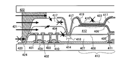
In this embodiment, another embodiment of the present invention will be described with reference to FIG. Note that the same parts as those in FIG. 1 may not be particularly described.
本実施の形態では配線401~405と画素電極(第1の電極)406が異なる層に形成
されている場合の例を説明する。本実施の形態では、第1の層間絶縁膜407上に絶縁膜
408が形成されている。第1の層間絶縁膜407はアクリルやポリイミドなどの有機絶
縁膜か、シロキサンなど、比較的透水性の高い絶縁膜を用いることを想定している。また
、絶縁膜408は窒化珪素や酸素を含む窒化珪素、窒素を含む酸化珪素、酸化珪素など透
水性の小さい膜で形成する。
In this embodiment mode, an example in which the
なお、第1の層間絶縁膜407とゲート電極、ゲート絶縁膜との間にさらに何層か絶縁膜
を形成してもかまわない。
Further, several insulating films may be formed between the first
絶縁膜408上には絶縁膜408と第1の層間絶縁膜407に開口されたコンタクトホー
ルを介して半導体層409~411に電気的に接続する電極(配線)401~405が形
成されている。
Electrodes (wirings) 401 to 405 electrically connected to the semiconductor layers 409 to 411 through contact holes opened in the insulating
絶縁膜408と電極(配線)401~405は第2の層間絶縁膜412で覆われており、
第2の層間絶縁膜412には画素部413の薄膜トランジスタの電極405に達するコン
タクトホールと、画素部413の周囲を一周して形成されている第1の開口部414が形
成されており、第1の開口部414は第2の層間絶縁膜を貫通している。なお、第1の開
口部414は、本実施の形態のように駆動回路部425が同一基板上に形成されている場
合は、図3のように駆動回路部425と画素部413との間に形成する。なお、駆動回路
が一体形成されていない発光装置であっても本発明を適用することが可能であり、画素部
の外周に開口部を形成すればよい。
The insulating
A contact hole reaching the
第2の層間絶縁膜412上には、当該第2の層間絶縁膜412に形成されたコンタクトホ
ールを介して薄膜トランジスタの電極405に電気的に接続する発光素子416の第1の
電極406が形成されている。
A
第2の層間絶縁膜412上には第1の電極406のコンタクトホール部及び端部を覆って
隔壁417が形成されている。隔壁417には第2の層間絶縁膜412に形成されている
第1の開口部414と同じ位置に第2の開口部418が形成されている。すなわち第1の
開口部と第2の開口部は重なるように設けられている。第2の開口部418はその底面が
第1の開口部414の内側に形成されており、絶縁膜408まで達している。第2の開口
部418も第1の開口部と同様、画素部413の周囲を囲んで形成されている。
A
なお、第1の電極406に面する隔壁417の端部は曲率を有し、当該曲率が連続的に変
化するテーパー形状をしていることが望ましい。また、隔壁417の一部と第1の電極4
06を覆って発光膜423が形成されており、隔壁417の一部と発光膜423を覆って
第2の電極419が形成されている。当該第2の電極419は隔壁417に形成された第
2の開口部418の側面及び底面を覆っている。
Note that an end portion of the
A light-emitting
なお、第2の層間絶縁膜及び隔壁の材料にはアクリルやポリイミドなどの有機絶縁膜やシ
ロキサンなどが多く用いられ、これらは比較的高い透水性を有していることが知られてい
る。そのためシール材を介して侵入した外部からの水分がこれらの膜を介して発光膜42
3に到達してしまうことが懸念されるが、本発明の構成を有する発光装置では、第1の層
間絶縁膜407に形成された第1の開口部414、隔壁417に形成された第2の開口部
418及び第2の開口部418の底面及び底面に形成された第2の電極419により外部
より侵入した水分が発光膜423へ到達するための経路は遮断されている。
Note that organic insulating films such as acrylic and polyimide, siloxane, and the like are often used as materials for the second interlayer insulating film and the partition walls, and are known to have relatively high water permeability. As a result, moisture from the outside entering through the sealant passes through these films to the light-emitting film 42 .
However, in the light-emitting device having the structure of the present invention, the
このように素子が形成された基板420はシール材421により対向基板422に固着さ
れ、発光装置となる。
The
このような構成を採ることによって、発光素子の第1の電極406が配線401~405
と異なる層に形成される、層間絶縁膜を2層有する構成であっても、外部から侵入する水
分による発光膜423の劣化を減少させることができる。また、発光素子416寿命を延
ばすことができ、発光装置の信頼性が向上する。すなわち、本発明の発光装置は外部雰囲
気よりシール材421を透過してきてしまった水分の経路が遮断されている構造である。
By adopting such a configuration, the
Even with a structure having two interlayer insulating films formed in different layers, deterioration of the
簡単に水分の侵入経路について説明する。まず、第1の層間絶縁膜407経由で侵入する
水分は絶縁膜408が存在することによってそれより発光膜423側へ侵入することがで
きない。また、図3に示したように第1の層間絶縁膜407の周辺端部を透水性の小さい
膜424で覆うと、第1の層間絶縁膜407へ侵入する水分の絶対量自体を減らすことが
できるので有効である。
A brief description will be given of the route of entry of moisture. First, moisture entering via the first
次に第2の層間絶縁膜412及び隔壁417へシール材421を介して侵入してきた水分
に関しては、第1の開口部414、第2の開口部418及び第2の開口部の底面及び底面
を覆っている第2の電極419により、それ以上発光膜423側へ侵入することが困難な
構造となっている。第2の開口部418の底面に形成された第2の電極419は絶縁膜4
08と接しており、水分の侵入を阻んでいる。また、本実施の形態では、第2の開口部4
18の底面に形成された第2の電極419は絶縁膜408と接しているが、実施の形態1
に示した構造(図1に示した接触部130)のように配線401~405と同じ材料で接
触部を形成しても良い。
Next, with regard to moisture entering the second
08 and prevents moisture from entering. Moreover, in the present embodiment, the second opening 4
A
1 (the
(実施の形態4)
本実施の形態では図4を用いて本発明の他の実施の形態について説明する。尚、図1及び
図3と同じ部分に関しては特に説明を行わないこともある。
(Embodiment 4)
In this embodiment, another embodiment of the present invention will be described with reference to FIG. Note that the same parts as those in FIGS. 1 and 3 may not be particularly described.
本実施の形態では配線501~505と画素電極(第1の電極)506が異なる層に形成
されている場合の例を説明する。本実施の形態では、第1の層間絶縁膜507は酸化珪素
や窒化珪素、窒素を含む酸化珪素及び酸素を含む窒化珪素などの材料で形成した例を示す
。第1の層間絶縁膜507は単層でも良いし、複数層であっても良い。これらの材料は透
水性が小さいため、外周部が外気に曝されていても水分がほとんど侵入しないことから図
3のように第1の層間絶縁膜の端面を透水性の小さい膜で覆わずとも水分は第1の層間絶
縁膜507にほとんど侵入しない。そのため、図3の絶縁膜408に相当する構成は形成
しなくても良い。その他の構成に関しては実施の形態3と同様である。
In this embodiment mode, an example in which the
図4(A)は従来の発光装置の断面図である。従来の構成では外部よりシール材508を
介して侵入した水分は内部雰囲気509、隔壁510、第2の層間絶縁膜511中を移動
しながら隔壁510より発光膜512へ到達し、発光膜512の劣化を引き起こす。なお
、本実施の形態の場合は第1の層間絶縁膜507は透水性が非常に小さい材料で形成させ
ることが前提であるため、第1の層間絶縁膜507経由の水分は考慮せずとも良い。
FIG. 4A is a cross-sectional view of a conventional light emitting device. In the conventional structure, water entering from the outside through the sealing
一方、図4(B)は本発明を適用した発光装置の断面図である。図4(B)では透水性の
高い材料で形成されている第2の層間絶縁膜511と隔壁510にそれぞれ第1の開口部
513と第2の開口部514が形成され、第2の開口部514の底面及び底面は発光素子
516の第2の電極515で覆われている。第1の開口部513と第2の開口部514は
画素部を一周するように形成されており、外部から侵入してきた水分が第2の層間絶縁膜
511及び隔壁510を介して発光膜512へ到達する経路を遮断している。
On the other hand, FIG. 4B is a cross-sectional view of a light emitting device to which the invention is applied. In FIG. 4B, a
このような構成を採ることによって、外部から水分が侵入することを抑制できる。また、
発光膜512の劣化を減少させることができるため、発光素子516の寿命を延ばすこと
ができ、発光装置の信頼性が向上する。
By adopting such a configuration, it is possible to suppress intrusion of moisture from the outside. again,
Since deterioration of the light-emitting
(実施の形態5)
本実施の形態では図5、及び図7を用いて本発明の他の実施の形態について説明する。尚
、図1、図3と同じ部分に関しては特に説明を行わない場合もある。
(Embodiment 5)
In this embodiment, another embodiment of the present invention will be described with reference to FIGS. 5 and 7. FIG. 1 and 3 may not be particularly described.
本実施の形態では、図1または図3とほぼ同様の構成であって、層間絶縁膜600上に透
水性の小さい絶縁膜(109、408に相当)を形成しない構造について、図5または図
7を参照しながら説明する。
In this embodiment, a structure having a configuration substantially similar to that of FIG. 1 or FIG. will be described with reference to.
図5(A)の構成においては、隔壁601において、開口部602を画素部603の外周
に形成し、開口部602の底面及び底面を発光素子604の第2の電極605で覆ってい
るため、水分の侵入をブロックすることができる。
In the structure of FIG. 5A, in the
また図5(B)に示す構成では、引き回し配線部608と駆動回路部609との間におい
て、層間絶縁膜600及びゲート絶縁膜、下地絶縁膜などに開口部610を形成している
。開口部610の側面及び底面を透水性の小さい膜611で覆っている。さらに、発光素
子604の第2の電極605の端部を透水性の小さい膜611と接するように形成するこ
とで、シール材606を介して外部より侵入する水分が層間絶縁膜600及び隔壁601
に侵入することを抑制することができる。なお、透水性の小さい膜611は画素部603
や駆動回路部609に形成される薄膜トランジスタの配線又は電極612~616と同じ
材料で形成し、同時に加工すれば工程の増加がない。
In the structure shown in FIG. 5B, an
can be prevented from invading Note that the
If they are formed from the same material as the wirings or
なお、本実施の形態では層間絶縁膜600に形成した開口部610は駆動回路部より外側
に形成されることとなるため、外部より信号を受け取る配線引き込み部(図15の(a)
に示す領域)においては画素部603全てを囲うことができないが、本発明の効果を発揮
することができ、信頼性の向上につながる。
In the present embodiment, the
2) cannot surround the
また、薄膜トランジスタの電極又は配線と、画素電極(第1の電極に相当)とが異なる層
に形成されており、第1の層間絶縁膜上に透水性の小さい絶縁膜が形成されていない場合
であっても、画素部と駆動回路部の間に開口部を形成する形態(実施の形態3、図3(B
)において絶縁膜408が無い場合)では、図5(A)に示すように本発明の開口部を設
けることにより、水分の侵入をブロックすることができる。
In addition, an electrode or wiring of a thin film transistor and a pixel electrode (corresponding to a first electrode) are formed in different layers, and an insulating film with low water permeability is not formed over the first interlayer insulating film. Even if there is, an opening is formed between the pixel portion and the driver circuit portion (Embodiment 3, FIG. 3B
) without the insulating film 408), by providing the opening of the present invention as shown in FIG. 5A, entry of moisture can be blocked.
また図7(B)に示した本実施の形態のように、駆動回路部705より外周部において第
1の層間絶縁膜702及びゲート絶縁膜、下地絶縁膜などに開口部707を形成している
。開口部707の側面及び底面を透水性の小さい膜708で覆う。さらに、発光素子70
9の第2の電極710の端部を透水性の小さい膜708と接するように形成する。その結
果シール材700を介して外部より侵入する水分が第1の層間絶縁膜702、第2の層間
絶縁膜701及び隔壁703に侵入することを抑制することができる。なお、透水性の小
さい膜708は画素部711や駆動回路部705に形成される薄膜トランジスタの配線又
は電極712~716と同じ材料で形成し、同時に加工すれば工程の増加がないので望ま
しい。
Further, as in this embodiment mode shown in FIG. 7B,
The end of the
なお、本実施の形態において開口部707は第1の層間絶縁膜702への水分の侵入を抑
制するため、第1の層間絶縁膜702に形成されており、第1の層間絶縁膜702の上と
下に密に配線が形成されている配線引き込み部(図15の(a)に示す領域)では上下の
配線のショートを防ぐ必要がある。そのため、本構成では画素部711全てを囲ってしま
うことはできないが、本発明の効果を発揮することができ、信頼性の向上につながる。
Note that in this embodiment, the
(実施の形態6)
本実施の形態では、本発明の一形態に相当する発光装置のパネルの外観の一例について図
14を用いて説明する。図14は基板上に形成されたトランジスタおよび発光素子を対向
基板4006との間に形成したシール材によって封止したパネルの上面図であり、実施の
形態1乃至実施の形態5のうちいずれかの構成を有している。
(Embodiment 6)
In this embodiment mode, an example of the appearance of a panel of a light-emitting device which corresponds to one embodiment of the present invention will be described with reference to FIGS. FIG. 14 is a top view of a panel in which a transistor and a light-emitting element formed over a substrate are sealed with a sealing material formed between a
基板4001上に形成された画素部4002と信号線駆動回路4003と走査線駆動回路
4004とを囲むようにして、シール材4005が形成されている。また、画素部400
2と信号線駆動回路4003と、走査線駆動回路4004の上に対向基板4006が形成
されている。よって画素部4002と信号線駆動回路4003と、走査線駆動回路400
4とは基板4001とシール材4005と対向基板4006とによって充填材と共に密封
されている。また、信号線駆動回路4003及び走査線駆動回路4004と、画素部40
02との間にはその底面と底面を発光素子の第2の電極で覆われた開口部4000が形成
されている。
A
2, a signal
4 is sealed by a
02, an
また、基板4001上に形成された画素部4002と信号線駆動回路4003と走査線駆
動回路4004とは薄膜トランジスタを複数有している。
A
また、引き回し配線は画素部4002と信号線駆動回路4003と、走査線駆動回路40
04とに、信号、または電源電圧を層供給すると目の配線に相当する。引き回し配線は、
接続端子と接続されており、接続端子はフレキシブルプリントサーキット(FPC)40
18が有する端子と異方性導電膜を介して電気的に接続されている。
In addition, the lead-out wiring is the
04 corresponds to wiring for supplying a signal or power supply voltage. The routing wiring is
It is connected to a connection terminal, and the connection terminal is a flexible printed circuit (FPC) 40
18 is electrically connected through an anisotropic conductive film.
なお、充填材としては窒素やアルゴンなどの不活性な気体の他に、紫外線硬化樹脂または
熱硬化樹脂を用いることができ、ポリビニルクロライド、アクリル、ポリイミド、エポキ
シ樹脂、シリコン樹脂、ポリビニルブチラル、またはエチレンビニレンアセテートを用い
る事ができる。
In addition to inert gases such as nitrogen and argon, the filler can be an ultraviolet curable resin or a thermosetting resin, such as polyvinyl chloride, acrylic, polyimide, epoxy resin, silicon resin, polyvinyl butyral, Ethylene vinylene acetate can be used.
図15は実施の形態5に示したような構成である場合の開口部の形成位置を示している。
このような構成である場合には、実施の形態5にも述べたように、外部からの信号を引き
込んで来る引き込み配線部分(図15(a))において開口部4000を形成するとショ
ートしてしまうため、画素部4002を開口部4000でもって完全に囲ってしまうこと
ができない。
FIG. 15 shows the formation positions of the openings in the case of the configuration shown in the fifth embodiment.
In such a configuration, as described in the fifth embodiment, if an
なお、本発明の表示装置は発光素子を有する画素部が形成されたパネルと、該パネルにI
Cが実装されたモジュールとをその範疇に含む。
Note that the display device of the present invention includes a panel in which a pixel portion having a light-emitting element is formed, and an I
C-implemented modules are included in this category.
(実施の形態7)
実施の形態6にその一例を示したようなモジュールを搭載した本発明の電子機器として、
ビデオカメラ、デジタルカメラ、ゴーグル型ディスプレイ(ヘッドマウントディスプレイ
)、ナビゲーションシステム、音響再生装置(カーオーディオコンポ等)、ノート型パー
ソナルコンピュータ、ゲーム機器、携帯情報端末(モバイルコンピュータ、携帯電話、携
帯型ゲーム機または電子書籍等)、記録媒体を備えた画像再生装置(具体的にはDigital
Versatile Disc(DVD)等の記録媒体を再生し、その画像を表示しうるディスプレイを
備えた装置)などが挙げられる。それらの電子機器の具体例を図16に示す。
(Embodiment 7)
As an electronic device of the present invention equipped with a module such as one example of which is shown in Embodiment 6,
Video cameras, digital cameras, goggle-type displays (head-mounted displays), navigation systems, audio playback devices (car audio components, etc.), notebook personal computers, game machines, personal digital assistants (mobile computers, mobile phones, portable game machines) or e-books, etc.), an image playback device equipped with a recording medium (specifically, Digital
a device that reproduces a recording medium such as a Versatile Disc (DVD) and has a display capable of displaying the image). Specific examples of those electronic devices are shown in FIG.
図16(A)は発光装置でありテレビ受像器などがこれに当たる。筐体2001、表示部
2003、スピーカー部2004等を含む。本発明の発光装置は、表示部2003におけ
る発光素子の劣化が抑制され、信頼性が向上する。画素部にはコントラストを高めるため
、偏光板、又は円偏光板を備えるとよい。例えば、封止基板へ1/4λ板、1/2λ板、
偏光板の順にフィルムを形成するとよい。さらに偏光板上に反射防止膜を形成してもよい
。
FIG. 16A shows a light-emitting device such as a television receiver. A
It is preferable to form the film in the order of the polarizing plate. Furthermore, an antireflection film may be formed on the polarizing plate.
図16(B)は携帯電話であり、本体2101、筐体2102、表示部2103、音声入
力部2104、音声出力部2105、操作キー2106、アンテナ2108等を含む。本
発明の携帯電話は、表示部2103における発光素子の劣化が抑制され、信頼性が向上す
る。
FIG. 16B shows a mobile phone including a
図16(C)はノート型パーソナルコンピュータであり、本体2201、筐体2202、
表示部2203、キーボード2204、外部接続ポート2205、ポインティングマウス
2206等を含む。本発明のノート型パーソナルコンピュータは、表示部2203におけ
る発光素子の劣化が抑制され、信頼性が向上する。
FIG. 16C shows a notebook personal computer including a
It includes a
図16(D)はモバイルコンピュータであり、本体2301、表示部2302、スイッチ
2303、操作キー2304、赤外線ポート2305等を含む。本発明のモバイルコンピ
ュータは、表示部2302における発光素子の劣化が抑制され、信頼性が向上する。
FIG. 16D shows a mobile computer including a
図16(E)は携帯型のゲーム機であり、筐体2401、表示部2402、スピーカー部
2403、操作キー2404、記録媒体挿入部2405等を含む。本発明の携帯型ゲーム
機は表示部2402における発光素子の劣化が抑制され、信頼性が向上する。
FIG. 16E shows a portable game machine including a
以上の様に、本発明の適用範囲は極めて広く、あらゆる分野の電子機器に用いることが可
能である。
As described above, the scope of application of the present invention is extremely wide, and it can be used in electronic devices in all fields.
本実施例では本発明の発光装置を作成する方法について図8、図9を参照しながら説明す
る。
In this embodiment, a method for manufacturing the light emitting device of the present invention will be described with reference to FIGS. 8 and 9. FIG.
基板800上に絶縁層801を形成した後、さらに半導体層を絶縁層801上に形成する
。(図8(A))
After forming the insulating
基板800の材料としては透光性を有するガラス、石英やプラスチック(ポリイミド、ア
クリル、ポリエチレンテレフタラート、ポリカーボネート、ポリアクリレート、ポリエー
テルスルホンなど)等を用いることができる。これら基板は必要に応じてCMP等により
研磨してから使用しても良い。本実施例においてはガラス基板を用いる。
As a material for the
絶縁層801は基板800中のアルカリ金属やアルカリ土類金属など、半導体膜の特性に
悪影響を及ぼすような元素が半導体層中に拡散するのを防ぐ為に形成する。材料としては
酸化珪素、窒化珪素、窒素を含む酸化珪素、酸素を含む窒化珪素などを用いることができ
、単層、または積層構造とすることにより形成する。なお、アルカリ金属やアルカリ土類
金属の拡散が心配ないようであれば特に絶縁層801は形成する必要がない。
The insulating
続いて形成される半導体層は本実施の形態では非晶質珪素膜をレーザ結晶化して得る。絶
縁層801上に非晶質珪素膜を25~100nm(好ましくは30~60nm)の膜厚で
形成する。形成方法としては公知の方法、例えばスパッタ法、減圧CVD法またはプラズ
マCVD法などが使用できる。その後、500℃で1時間の加熱処理を行い、水素出しを
する。
The subsequently formed semiconductor layer is obtained by laser crystallization of an amorphous silicon film in this embodiment. An amorphous silicon film is formed on the insulating
続いてレーザ照射装置を用いて非晶質珪素膜を結晶化して結晶質珪素膜を形成する。本実
施の形態のレーザ結晶化ではエキシマレーザを使用し、発振されたレーザビームを光学系
を用いて線状のビームスポットに加工し非晶質珪素膜に照射することで結晶質珪素膜とし
、半導体層として用いる。
Subsequently, the amorphous silicon film is crystallized using a laser irradiation device to form a crystalline silicon film. In the laser crystallization of the present embodiment, an excimer laser is used, and an oscillated laser beam is processed into a linear beam spot using an optical system and irradiated onto an amorphous silicon film to form a crystalline silicon film, Used as a semiconductor layer.
非晶質珪素膜の他の結晶化の方法としては、他に、熱処理のみにより結晶化を行う方法や
結晶化を促進する触媒元素を用い加熱処理を行う事によって行う方法もある。結晶化を促
進する元素としてはニッケル、鉄、パラジウム、錫、鉛、コバルト、白金、どう、金など
が挙げられ、このような元素を用いることによって熱処理のみで結晶化を行った場合に比
べ、低温、短時間で結晶化が行われるため、ガラス基板などへのダメージが少ない。熱処
理のみにより結晶化をする場合は、基板800を熱に強い石英基板などにしなければいけ
ない。
Other methods for crystallizing the amorphous silicon film include a method of crystallizing only by heat treatment and a method of performing heat treatment using a catalyst element that promotes crystallization. Examples of elements that promote crystallization include nickel, iron, palladium, tin, lead, cobalt, platinum, gold, and gold. Crystallization takes place at a low temperature in a short period of time, so there is little damage to glass substrates, etc. When crystallization is performed only by heat treatment, the
続いて、必要に応じて半導体層にしきい値をコントロールする為に微量の不純物添加、い
わゆるチャネルドーピングを行う。要求されるしきい値を得る為にN型もしくはP型を呈
する不純物(リン、ボロンなど)をイオンドーピング法などにより添加する。
Subsequently, if necessary, a small amount of impurity is added to the semiconductor layer, so-called channel doping, in order to control the threshold value. In order to obtain the required threshold value, an N-type or P-type impurity (phosphorus, boron, etc.) is added by an ion doping method or the like.
その後、図8(A)に示すように半導体層を所定の形状にパターニングし、島状の半導体
層802~804を得る。パターニングは半導体層にフォトレジストを塗布し、所定のマ
スク形状を露光し、焼成して、半導体層上にレジストマスクを形成し、このマスクを用い
てエッチングをすることにより行われる。
After that, as shown in FIG. 8A, the semiconductor layer is patterned into a predetermined shape to obtain island-shaped semiconductor layers 802 to 804 . Patterning is performed by applying a photoresist to the semiconductor layer, exposing it to a predetermined mask shape, baking it, forming a resist mask on the semiconductor layer, and etching using this mask.
続いて半導体層802~804を覆うようにゲート絶縁膜805を形成する。ゲート絶縁
膜805はプラズマCVD法またはスパッタ法を用いて膜厚を40~150nmとして珪
素を含む絶縁膜で形成する。
Subsequently, a
次いで、ゲート絶縁膜805上にゲート電極806~808を形成する。ゲート電極80
6~808はTa、W、Ti、Mo、Al、Cu、Cr、Ndから選ばれた元素、または
前記元素を主成分とする合金材料若しくは化合物材料で形成してもよい。また、リン等の
不純物元素をドーピングした多結晶珪素膜に代表される半導体膜を用いてもよい。また、
AgPdCu合金を用いてもよい。
Next,
6 to 808 may be made of an element selected from Ta, W, Ti, Mo, Al, Cu, Cr, and Nd, or an alloy material or compound material containing said element as a main component. A semiconductor film typified by a polycrystalline silicon film doped with an impurity element such as phosphorus may also be used. again,
AgPdCu alloys may also be used.
また、本実施の形態ではゲート電極806~808は単層で形成されているが、下層にタ
ングステン、上層にモリブデンなどの2層以上の積層構造でもかまわない。積層構造とし
てゲート電極を形成する場合であっても前段で述べた材料を使用するとよい。また、その
組み合わせも適宜選択すればよい。
In addition, although the
ゲート電極806~808の加工はフォトレジストを用いたマスクを利用し、エッチング
をして行う。
The
続いて、ゲート電極806~808をマスクとして半導体層802~804に高濃度の不
純物を添加する。これによって半導体層802~804、ゲート絶縁膜805、及びゲー
ト電極806~808を含む薄膜トランジスタが形成される。
Subsequently, high-concentration impurities are added to the semiconductor layers 802 to 804 using the
なお、薄膜トランジスタの作製工程については特に限定されず、所望の構造のトランジス
タを作製できるように適宜変更すればよい。
Note that the manufacturing process of the thin film transistor is not particularly limited, and may be changed as appropriate so that a transistor with a desired structure can be manufactured.
本実施の形態では、レーザ結晶化を使用して結晶化した結晶性シリコン膜を用いたトップ
ゲートの薄膜トランジスタを用いたが、非晶質半導体膜を用いたボトムゲート型の薄膜ト
ランジスタを画素部に用いることも可能である。非晶質半導体は珪素だけではなくシリコ
ンゲルマニウムも用いることができ、シリコンゲルマニウムを用いる場合、ゲルマニウム
の濃度は0.01~4.5atomic%程度であることが好ましい。
In this embodiment mode, a top-gate thin film transistor using a crystalline silicon film crystallized by laser crystallization is used, but a bottom-gate thin film transistor using an amorphous semiconductor film is used in a pixel portion. is also possible. Not only silicon but also silicon germanium can be used as the amorphous semiconductor. When silicon germanium is used, the concentration of germanium is preferably about 0.01 to 4.5 atomic %.
また非晶質半導体中に0.5nm~20nmの結晶を粒観察することができる微結晶半導
体膜(セミアモルファス半導体)を用いてもよい。また0.5nm~20nmの結晶を粒
観察することができる微結晶はいわゆるマイクロクリスタル(μc)とも呼ばれている。
Alternatively, a microcrystalline semiconductor film (semi-amorphous semiconductor) in which crystal grains of 0.5 nm to 20 nm can be observed in an amorphous semiconductor may be used. Also, a microcrystal whose grain size can be observed from 0.5 nm to 20 nm is called a so-called microcrystal (μc).
セミアモルファス半導体であるセミアモルファスシリコン(SASとも表記する)は、珪
化物気体をグロー放電分解することにより得ることができる。代表的な珪化物気体として
は、SiH4であり、その他にもSi2H6、SiH2Cl2、SiHCl3、SiCl4、S
iF4などを用いることができる。この珪化物気体を水素、水素とヘリウム、アルゴン、
クリプトン、ネオンから選ばれた一種または複数種の希ガス元素で希釈して用いることで
SASの形成を容易なものとすることができる。希釈率は10倍~1000倍の範囲で珪
化物気体を希釈することが好ましい。グロー放電分解による被膜の反応生成は0.1Pa
~133Paの範囲の圧力で行えば良い。グロー放電を形成するための電力は1MHz~
120MHz、好ましくは13MHz~60MHzの高周波電力を供給すれば良い。基板
加熱温度は300度以下が好ましく、100~250度の基板加熱温度が好適である。
Semi-amorphous silicon (also referred to as SAS), which is a semi-amorphous semiconductor, can be obtained by glow discharge decomposition of silicide gas. A typical silicide gas is SiH 4 , and also Si 2 H 6 , SiH 2 Cl 2 , SiHCl 3 , SiCl 4 , S
iF4 or the like can be used. This silicide gas is hydrogen, hydrogen and helium, argon,
By diluting with one or more rare gas elements selected from krypton and neon, the formation of SAS can be facilitated. It is preferable to dilute the silicide gas at a dilution ratio of 10 to 1000 times. The reaction generation of the film by glow discharge decomposition is 0.1 Pa
A pressure in the range of up to 133 Pa may be used. Power to form glow discharge is 1MHz~
A high frequency power of 120 MHz, preferably 13 MHz to 60 MHz may be supplied. The substrate heating temperature is preferably 300°C or less, and a substrate heating temperature of 100 to 250°C is suitable.
このようにして形成されたSASはラマンスペクトルが520cm-1よりも低波数側にシ
フトしており、X線回折ではSi結晶格子に由来するとされる(111)、(220)の
回折ピークが観測される。未結合手(ダングリングボンド)の中和剤として水素またはハ
ロゲンを少なくとも1原子%またはそれ以上含ませている。膜中の不純物元素として、酸
素、窒素、炭素などの大気成分の不純物は1×1020cm-1以下とすることが望ましく、特
に、酸素濃度は5×10¹⁹/cm3以下、好ましくは1×1019/cm3以下とする。TFTにし
たときのμ=1~10cm2/Vsecとなる。また、このSASをレーザでさらに結晶化して用
いても良い。
The SAS thus formed has a Raman spectrum shifted to the lower wavenumber side than 520 cm −1 , and in X-ray diffraction, diffraction peaks of (111) and (220), which are thought to be derived from the Si crystal lattice, are observed. be done. At least 1 atomic % or more of hydrogen or halogen is contained as a neutralizing agent for dangling bonds. As impurity elements in the film, the impurities of atmospheric components such as oxygen, nitrogen, and carbon are desirably 1×10 20 cm −1 or less, and in particular, the oxygen concentration is 5×10 19 /cm 3 or less, preferably 1×10 19 cm −1 or less. ×10 19 /cm 3 or less. μ=1 to 10 cm 2 /Vsec in the case of TFT. Further, this SAS may be further crystallized by a laser and used.
続いて、ゲート電極806~808、ゲート絶縁膜805を覆う層間絶縁膜809を形成
する。層間絶縁膜809を形成する材料としては酸化珪素、アクリル、ポリイミドや珪素
と酸素との結合で骨格構造が構成され、置換基に少なくとも水素を含む、または置換基に
フッ素、アルキル基、または芳香族炭化水素のうち少なくとも1種を有する材料、シロキ
サン、Iow-k材料等の材料で形成すればよい。本実施例ではシロキサンを層間絶縁膜
809として形成した。(図8(B))
Subsequently, an
次に、層間絶縁膜809上に透水性の小さい材料によって絶縁膜810を成膜する。絶縁
膜810は窒化珪素や酸素を有する窒化珪素、酸化珪素、窒素を有する酸化珪素などを用
いるとよい。
Next, an insulating
続いて、絶縁膜810、層間絶縁膜809及びゲート絶縁膜805を貫通して半導体層8
02~804に至るコンタクトホールを形成すると共に基板周辺部において少なくとも絶
縁膜810、層間絶縁膜809及びゲート絶縁膜805を除去する。(図8(C))
Subsequently, the semiconductor layer 8 is formed through the insulating
02 to 804 are formed, and at least the insulating
コンタクトホールの形成と基板周辺部の絶縁膜除去はレジストを用いてエッチングにより
行えば良いが、層間絶縁膜809、絶縁膜810及びゲート電極802~804の材料に
よっては条件を変えて複数のエッチングによりコンタクトホールを形成する方が良い場合
がある。
The formation of the contact holes and the removal of the insulating film in the peripheral portion of the substrate may be performed by etching using a resist. Forming a contact hole may be better.
そして、当該コンタクトホールや層間絶縁膜809を覆う導電層を形成する。当該導電層
を所望の形状に加工し、配線(電極)811~815、引き回し配線816及び接触部8
17を形成する。これらはアルミニウム、銅等の単層でも良いが、本実施の形態ではモリ
ブデン、アルミニウム、モリブデンの順に形成された積層構造とする。積層配線としては
チタン、アルミニウム、チタンの順に形成された積層構造やチタン、窒化チタン、アルミ
ニウム、チタンの順に形成された積層構造でも良い。また、引き回し配線816は層間絶
縁膜809等の端面を覆うカバー膜としての役割も有する。接触部817は画素部822
と駆動回路部823との間に画素部822を囲むように一周させる。
Then, a conductive layer is formed to cover the contact hole and the
17 is formed. These may be single layers of aluminum, copper, or the like, but in the present embodiment, they have a laminated structure in which molybdenum, aluminum, and molybdenum are formed in this order. As the laminated wiring, a laminated structure formed in order of titanium, aluminum and titanium or a laminated structure formed in order of titanium, titanium nitride, aluminum and titanium may be used. The lead-out
and the
これにより、駆動回路部の薄膜トランジスタと画素部の薄膜トランジスタが完成する。8
18は駆動回路部の薄膜トランジスタの一部を表し、819が画素部の薄膜トランジスタ
の一部を表している。
Thus, the thin film transistors of the drive circuit portion and the thin film transistors of the pixel portion are completed. 8
Reference numeral 18 denotes a portion of the thin film transistor in the driver circuit portion, and 819 denotes a portion of the thin film transistor in the pixel portion.
そして画素部の薄膜トランジスタ819の電極815を覆って、透光性を有する導電層を
形成したのち、当該透光性を有する導電層を加工して第1の電極820を形成する。ここ
で第1の電極820は薄膜トランジスタ819の電極815と電気的に接触しておいる。
第1の電極820の材料としてはインジウム錫酸化物(ITO:Indium Tin Oxide)や酸
化珪素を含有するITO、酸化インジウムに2~20%の酸化亜鉛を含有したIZO(In
dium Zinc Oxide)もしくは酸化亜鉛そのもの、そして酸化亜鉛にガリウムを含有したG
ZO(Galium Zinc Oxide)等を用いるとよい。(図8(D))
After a light-transmitting conductive layer is formed to cover the
Materials for the
Zinc Oxide) or zinc oxide itself, and zinc oxide containing gallium
ZO (Galium Zinc Oxide) or the like is preferably used. (Fig. 8(D))
次に絶縁膜810及び第1の電極820を覆って有機材料もしくは無機材料からなる絶縁
膜を形成する。続いて当該絶縁層は第1の電極の一部が露出するように加工し、隔壁82
1を形成する。隔壁821の材料としては、感光性を有する有機材料(アクリル、ポリイ
ミドなど)が好適に用いられるが、感光性を有さない有機材料や無機材料で形成してもか
まわない。隔壁821の第1の電極に面した端面は曲率を有し、当該曲率が連続的に変化
するテーパー形状をしていることが望ましい。なお、隔壁821に顔料やカーボンなど黒
色の物質を混入し、ブラックマトリクスとして用いても良い。(図9(A))
Next, an insulating film made of an organic material or an inorganic material is formed to cover the insulating
1 is formed. As a material of the
また、画素部822と駆動回路部823との間に画素部822の周囲を一周して開口部
824を形成する。開口部824の底面には接触部817が露出するように接触部817
と同位置に形成する。
In addition, an
formed at the same position as
次に、隔壁821から露出した第1の電極820を覆う発光層825を形成する。発光層
825は蒸着法やインクジェット法、スピンコート法などいずれの方法を用いて形成して
もかまわない。(図9(B))
Next, a light-emitting
続いて発光層825を覆う第2の電極826を形成する。これによって第1の電極820
と発光層825と第2の電極826とからなる発光素子827を形成することができる。
第2の電極826は開口部824まで覆うように成膜し、開口部824の底面及び底面を
覆うように形成する。
Subsequently, a
A light-emitting
The
その後、プラズマCVD法により窒素を含む酸化珪素膜をパッシベーション膜として形成
しても良い。窒素を含む酸化珪素膜を用いる場合には、プラズマCVD法でSiH4、N2
O、NH3から形成される酸化窒化ケイ素膜、またはSiH4、N2Oから形成される酸化
窒化ケイ素膜、あるいはSiH4、N2OをArで希釈したガスから形成される酸化窒化ケ
イ素膜を形成すれば良い。
After that, a silicon oxide film containing nitrogen may be formed as a passivation film by plasma CVD. When a silicon oxide film containing nitrogen is used, SiH 4 and N 2 are deposited by plasma CVD.
A silicon oxynitride film formed from O and NH 3 , a silicon oxynitride film formed from SiH 4 and N 2 O, or a silicon oxynitride film formed from a gas obtained by diluting SiH 4 and N 2 O with Ar should be formed.
また、パッシベーション膜としてSiH4、N2O、H2から形成される酸化窒化水素化ケ
イ素膜を適用しても良い。もちろん、パッシベーション膜は単層構造に限定されるもので
はなく、ケイ素を含む他の絶縁膜を単層構造、もしくは積層構造として用いても良い。ま
た、窒化炭素膜と窒化ケイ素膜の多層膜やスチレンポリマーの多層膜、窒化ケイ素膜やダ
イヤモンドライクカーボン膜を、窒素を含む酸化珪素膜の代わりに形成してもよい。
Also, a hydrogenated silicon oxynitride film formed from SiH 4 , N 2 O, and H 2 may be applied as the passivation film. Of course, the passivation film is not limited to a single-layer structure, and other insulating films containing silicon may be used in a single-layer structure or a laminated structure. Also, a multilayer film of a carbon nitride film and a silicon nitride film, a multilayer film of styrene polymer, a silicon nitride film, or a diamond-like carbon film may be formed instead of the nitrogen-containing silicon oxide film.
続いて表示部の封止を行う。対向基板829を封止に用いる場合は、絶縁性のシール材8
28により、外部接続部が露出するように貼り合わせる。対向基板829には凹部を形成
して乾燥材830を貼り付けても良い。対向基板829と素子が形成された基板800と
の間の空間には乾燥した窒素などの不活性気体を充填しても良いし、シール材828を画
素部全面に塗布しそれにより対向基板を形成しても良い。シール材には紫外線硬化樹脂な
どを用いると好適である。シール材には乾燥材やギャップを一定に保つための粒子を混入
しておいても良い。続いて外部接続部にフレキシブル配線基板を貼り付けることによって
、発光装置が完成する。
Subsequently, the display portion is sealed. When the
By 28, they are stuck together so that the external connection portion is exposed. A recess may be formed in the
なお、表示機能を有する本発明の発光表示装置には、アナログのビデオ信号、デジタルの
ビデオ信号のどちらを用いてもよい。デジタルのビデオ信号を用いる場合はそのビデオ信
号が電圧を用いているものと、電流を用いているものとに分けられる。発光素子の発光時
において、画素に入力されるビデオ信号は、発光素子に印加される電圧を一定に制御する
定電圧駆動と、発光素子に流れる電流を一定に制御する定電流駆動とがある。定電流駆動
は、発光素子の劣化、温度変化等による抵抗値の変化によらず、一定の電流が流れるよう
に制御することができる。本発明の発光装置の駆動方法には、このような駆動方法のいず
れを適用しても構わない。
Note that either an analog video signal or a digital video signal may be used for the light-emitting display device of the present invention having a display function. When a digital video signal is used, it is divided into those using voltage and those using current. When the light emitting element emits light, the video signal input to the pixel is classified into constant voltage driving that controls the voltage applied to the light emitting element constant and constant current driving that controls the current flowing through the light emitting element constant. Constant-current driving can be controlled so that a constant current flows regardless of changes in the resistance value due to deterioration of the light-emitting element, temperature change, or the like. Any of these driving methods may be applied to the driving method of the light emitting device of the present invention.
なお、図1(B)、図2(B)、図3(B)、図4(B)、図5(B)、図7(B)に示
した本発明の他の構成は本実施の形態で示した作成プロセスを適宜変更することで当業者
であれば容易に得ることができる。
1(B), 2(B), 3(B), 4(B), 5(B), and 7(B) of the present invention can It can be easily obtained by those skilled in the art by appropriately changing the creation process shown in the form.
本実施例では、画素構成の一例について図17(A)、(B)を参照しながら説明する。
本実施例では、図3、図4及び図7に示したような発光素子の第1の電極と薄膜トランジ
スタの電極が異なる層上に形成される場合に付いての画素構成である。なお、図17(B
)は本実施例における上面図であり、図17(A)は(B)におけるA-Bの断面図に相
当し、図17(B)において1012は発光膜、1009は補助配線、1010は隔壁で
ある。
In this embodiment, an example of a pixel configuration will be described with reference to FIGS.
In this embodiment, the pixel configuration is such that the first electrode of the light emitting element and the electrode of the thin film transistor are formed on different layers as shown in FIGS. Note that FIG.
) is a top view in this embodiment, FIG. 17A corresponds to a cross-sectional view along AB in FIG. 17B, and in FIG. is.
この場合、第1の電極1000が第2の層間絶縁膜1001上、薄膜トランジスタの電極
1002、1003が第1の層間絶縁膜1004上と、異なる層に形成されている為、第
2の電極1005を透明導電膜で形成し、発光した光が射出する方向を基板1006と反
対の方向(上面出射)とすると、発光素子1007と重なる位置に薄膜トランジスタ10
08を形成する事ができる。これは開口率の関係上、有利である。
In this case, since the
08 can be formed. This is advantageous in relation to the aperture ratio.
ところで、本実施例では第2の電極1005は透明導電膜で形成しているが、透明導電膜
は高抵抗なものが多い。第2の電極1005は画素部全面を覆うように形成するのだが、
透明導電膜であると抵抗が高いため、画素部周辺部と中央部で電圧降下により表示に影響
が出てしまう場合がある。
By the way, although the
Since the transparent conductive film has a high resistance, display may be affected due to a voltage drop between the periphery and the center of the pixel portion.
そこで本実施例では第1の電極1000と同じ層に低抵抗材料で補助配線1009を形成
し、それを第2の電極1005に接続する。補助配線1009は図17(B)のように画
素と画素との間にストライプ状に形成されており、隔壁1010に形成された開口部10
11を介して発光素子1007の第2の電極1005に画素部全体にわたって同様に接続
されている。
Therefore, in this embodiment, an
11 to the
この補助配線1009によって第2の電極1005の見かけの抵抗が下がって、電圧降下
が起こることを防ぐことができ、画素部全体において良好な表示を行うことが可能になる
。
The
このような補助配線1009は画素部の大部分に形成されなければ電圧降下を防ぐことが
できず、且つある程度の幅がなければ補助配線1009自身でも電圧降下が生じてしまう
為、有効に機能する程度の幅を有する補助配線1009を下層の第1の層間絶縁膜上に形
成することは困難である。しかし、第2の層間絶縁膜1001上に補助配線1009を形
成することによって、有効に機能しうる補助配線1009を形成することが可能となる。
Such an
なお、本実施例においては、隔壁1010に顔料やカーボンなど黒色の物質を混入し、ブ
ラックマトリクスとして用いても良い。
Note that in this embodiment, a black substance such as a pigment or carbon may be mixed into the
図17(C)は本実施例の他のパターンであり、補助配線が薄膜トランジスタの電極を兼
ねた構成となっている。
FIG. 17C shows another pattern of this embodiment, in which the auxiliary wiring also serves as the electrode of the thin film transistor.
本実施例では発光層825の構成について詳しく説明する。
In this embodiment, the structure of the light-emitting
発光膜は、有機化合物又は無機化合物を含む発光材料で形成された発光層を有する。有機
化合物は、その分子数から低分子系有機化合物、中分子系有機化合物(昇華性を有さず、
且つ分子数が20以下、又は連鎖する分子の長さが10μm以下の有機化合物を指してい
う)、高分子系有機化合物から選ばれた一種又は複数種の層を含む。また発光膜は、発光
層に加えて電子注入輸送性又は正孔注入輸送性の材料を有してもよく、当該材料は有機化
合物であっても、無機化合物であってもよい。
The light-emitting film has a light-emitting layer made of a light-emitting material containing an organic compound or an inorganic compound. Organic compounds are divided into low-molecular-weight organic compounds and middle-molecular-weight organic compounds (without sublimation,
and an organic compound having 20 or less molecules or a length of chained molecules of 10 μm or less), and includes one or more layers selected from polymeric organic compounds. In addition to the light-emitting layer, the light-emitting film may have an electron-injection-transporting material or a hole-injecting-transporting material, and the material may be an organic compound or an inorganic compound.
電荷注入輸送物質のうち、特に電子輸送性の高い物質としては、例えばトリス(8-キノ
リノラト)アルミニウム(略称:Alq3)、トリス(5-メチル-8-キノリノラト)
アルミニウム(略称:Almq3)、ビス(10-ヒドロキシベンゾ[h]-キノリナト)
ベリリウム(略称:BeBq2)、ビス(2-メチル-8-キノリノラト)-4-フェニ
ルフェノラト-アルミニウム(略称:BAlq)など、キノリン骨格またはベンゾキノリ
ン骨格を有する金属錯体等が挙げられる。また正孔輸送性の高い物質としては、例えば4
,4'-ビス[N-(1-ナフチル)-N-フェニル-アミノ]-ビフェニル(略称:α
-NPD)や4,4'-ビス[N-(3-メチルフェニル)-N-フェニル-アミノ]-
ビフェニル(略称:TPD)や4,4',4''-トリス(N,N-ジフェニル-アミノ)
-トリフェニルアミン(略称:TDATA)、4,4',4''-トリス[N-(3-メチ
ルフェニル)-N-フェニル-アミノ]-トリフェニルアミン(略称:MTDATA)な
どの芳香族アミン系(即ち、ベンゼン環-窒素の結合を有する)の化合物が挙げられる。
Among charge injecting and transporting substances, substances having particularly high electron transporting properties include, for example, tris(8-quinolinolato)aluminum (abbreviation: Alq 3 ) and tris(5-methyl-8-quinolinolato).
Aluminum (abbreviation: Almq 3 ), bis(10-hydroxybenzo[h]-quinolinato)
Metal complexes having a quinoline skeleton or benzoquinoline skeleton such as beryllium (abbreviation: BeBq 2 ), bis(2-methyl-8-quinolinolato)-4-phenylphenolato-aluminum (abbreviation: BAlq), and the like. As a substance with a high hole transport property, for example, 4
, 4′-bis[N-(1-naphthyl)-N-phenyl-amino]-biphenyl (abbreviation: α
-NPD) and 4,4'-bis[N-(3-methylphenyl)-N-phenyl-amino]-
Biphenyl (abbreviation: TPD) and 4,4',4''-tris (N,N-diphenyl-amino)
-triphenylamine (abbreviation: TDATA), 4,4′,4″-tris[N-(3-methylphenyl)-N-phenyl-amino]-triphenylamine (abbreviation: MTDATA) and other aromatic amines system (ie, having a benzene ring-nitrogen bond).
また、電荷注入輸送物質のうち、特に電子注入性の高い物質としては、フッ化リチウム(
LiF)、フッ化セシウム(CsF)、フッ化カルシウム(CaF2)等のようなアルカ
リ金属又はアルカリ土類金属の化合物が挙げられる。また、この他、Alq3のような電
子輸送性の高い物質とマグネシウム(Mg)のようなアルカリ土類金属との混合物であっ
てもよい。
Lithium fluoride (
LiF), cesium fluoride (CsF), calcium fluoride ( CaF2 ), and other compounds of alkali metals or alkaline earth metals. In addition, a mixture of a highly electron - transporting substance such as Alq3 and an alkaline earth metal such as magnesium (Mg) may be used.
電荷注入輸送物質のうち、正孔注入性の高い物質としては、例えば、モリブデン酸化物(
MoOx)やバナジウム酸化物(VOx)、ルテニウム酸化物(RuOx)、タングステ
ン酸化物(WOx)、マンガン酸化物(MnOx)等の金属酸化物が挙げられる。また、
この他、フタロシアニン(略称:H2Pc)や銅フタロシアニン(CuPC)等のフタロ
シアニン系の化合物が挙げられる。
Among charge injecting and transporting substances, molybdenum oxide (
MoOx), vanadium oxide (VOx), ruthenium oxide (RuOx), tungsten oxide (WOx), and manganese oxide (MnOx). again,
In addition, phthalocyanine compounds such as phthalocyanine (abbreviation: H 2 Pc) and copper phthalocyanine (CuPC) can be used.
発光層は、発光波長帯の異なる発光層を画素毎に形成して、カラー表示を行う構成として
も良い。典型的には、R(赤)、G(緑)、B(青)の各色に対応した発光層を形成する
。この場合にも、画素の光放射側にその発光波長帯の光を透過するフィルター(着色層)
を形成した構成とすることで、色純度の向上や、画素部の鏡面化(映り込み)の防止を図
ることができる。そのため、フィルター(着色層)を形成することで、画素部の鏡面化(
写り込み)を防止するために用いられていた円偏光板などを省略することが可能となり、
偏光板を用いた事によって約半分となっていた光の損失を無くすことができる。さらに、
斜方から画素部(表示画面)を見た場合に起こる色調の変化を低減すことができる。
The light-emitting layer may be configured to perform color display by forming light-emitting layers with different emission wavelength bands for each pixel. Typically, light-emitting layers corresponding to R (red), G (green), and B (blue) are formed. In this case also, a filter (colored layer) that transmits light in the emission wavelength band is provided on the light emitting side of the pixel.
is formed, it is possible to improve the color purity and prevent the pixel portion from becoming a mirror surface (reflection). Therefore, by forming a filter (colored layer), the pixel area is mirror-finished (
It is possible to omit the circularly polarizing plate etc. used to prevent reflection,
The use of the polarizing plate can eliminate the loss of light, which has been reduced to about half. moreover,
It is possible to reduce the change in color tone that occurs when the pixel portion (display screen) is viewed obliquely.
発光材料には様々な材料がある。低分子系有機発光材料では、4-ジシアノメチレン-2
-メチル-6-(1,1,7,7-テトラメチルジュロリジル-9-エニル) -4H-ピラン
(略称:DCJT)、4-ジシアノメチレン-2-t-ブチル-6-(1,1,7,7-テト
ラメチルジュロリジル-9-エニル) -4H-ピラン(略称:DPA)、ペリフランテン
、2,5-ジシアノ-1,4-ビス(10-メトキシ-1,1,7,7-テトラメチルジュロリ
ジル-9-エニル)ベンゼン、N,N’-ジメチルキナクリドン(略称:DMQd)、クマ
リン6、クマリン545T、トリス(8-キノリノラト)アルミニウム(略称:Alq3)
、9,9’-ビアントリル、9,10-ジフェニルアントラセン(略称:DPA)や9,1
0-ビス(2-ナフチル)アントラセン(略称:DNA)等を用いることができる。また、
この他の物質でもよい。
There are various kinds of luminescent materials. 4-dicyanomethylene-2 in low-molecular-weight organic light-emitting materials
-methyl-6-(1,1,7,7-tetramethyljulolidyl-9-enyl)-4H-pyran (abbreviation: DCJT), 4-dicyanomethylene-2-t-butyl-6-(1, 1,7,7-tetramethyljulolidyl-9-enyl)-4H-pyran (abbreviation: DPA), periflanthene, 2,5-dicyano-1,4-bis(10-methoxy-1,1,7, 7-tetramethyljulolidyl-9-enyl)benzene, N,N'-dimethylquinacridone (abbreviation: DMQd), coumarin 6, coumarin 545T, tris(8-quinolinolato)aluminum (abbreviation: Alq 3 )
, 9,9′-bianthryl, 9,10-diphenylanthracene (abbreviation: DPA) and 9,1
0-bis(2-naphthyl)anthracene (abbreviation: DNA) and the like can be used. again,
Other substances may be used.
一方、高分子系有機発光材料は低分子系に比べて物理的強度が高く、素子の耐久性が高い
。また塗布により成膜することが可能であるので、素子の形成が比較的容易である。高分
子系有機発光材料を用いた発光素子の構造は、低分子系有機発光材料を用いたときと基本
的には同じであり、TFT側から陰極、有機発光層、陽極の順に形成される。しかし、高
分子系有機発光材料を用いた発光層を形成する際には、低分子系有機発光材料を用いたと
きのような積層構造を形成させることは難しく、多くの場合2層構造となる。具体的には
、陰極、発光層。正孔輸送層、陽極の順に形成された積層構造である。
On the other hand, high-molecular-weight organic light-emitting materials have higher physical strength and higher device durability than low-molecular-weight materials. Moreover, since it is possible to form a film by coating, it is relatively easy to form an element. The structure of a light-emitting element using a high-molecular-weight organic light-emitting material is basically the same as when using a low-molecular-weight organic light-emitting material, and the cathode, organic light-emitting layer, and anode are formed in this order from the TFT side. However, when forming a light-emitting layer using a high-molecular-weight organic light-emitting material, it is difficult to form a layered structure as in the case of using a low-molecular-weight organic light-emitting material, and in many cases, a two-layer structure is formed. . Specifically, the cathode and the light-emitting layer. It has a laminated structure in which a hole transport layer and an anode are formed in this order.
発光色は、発光層を形成する材料で決まるため、これらを選択することで所望の発光を示
す発光素子を形成することができる。発光層の形成に用いることができる高分子系の電界
発光材料は、ポリパラフェニレンビニレン系、ポリパラフェニレン系、ポリチオフェン系
、ポリフルオレン系が挙げられる。
Since the emission color is determined by the material forming the light-emitting layer, a light-emitting element exhibiting desired emission can be formed by selecting these materials. Polymeric electroluminescent materials that can be used to form the light-emitting layer include polyparaphenylene vinylene, polyparaphenylene, polythiophene, and polyfluorene materials.
ポリパラフェニレンビニレン系には、ポリ(パラフェニレンビニレン) [PPV] の誘導
体、ポリ(2,5-ジアルコキシ-1,4-フェニレンビニレン) [RO-PPV]、ポ
リ(2-(2'-エチル-ヘキソキシ)-5-メトキシ-1,4-フェニレンビニレン)[
MEH-PPV]、ポリ(2-(ジアルコキシフェニル)-1,4-フェニレンビニレン)
[ROPh-PPV]等が挙げられる。ポリパラフェニレン系には、ポリパラフェニレン[
PPP]の誘導体、ポリ(2,5-ジアルコキシ-1,4-フェニレン)[RO-PPP]
、ポリ(2,5-ジヘキソキシ-1,4-フェニレン)等が挙げられる。ポリチオフェン
系には、ポリチオフェン[PT]の誘導体、ポリ(3-アルキルチオフェン)[PAT]
、ポリ(3-ヘキシルチオフェン)[PHT]、ポリ(3-シクロヘキシルチオフェン)
[PCHT]、ポリ(3-シクロヘキシル-4-メチルチオフェン)[PCHMT]、ポ
リ(3,4-ジシクロヘキシルチオフェン)[PDCHT]、ポリ[3-(4-オクチル
フェニル)-チオフェン][POPT]、ポリ[3-(4-オクチルフェニル)-2,2
ビチオフェン][PTOPT]等が挙げられる。ポリフルオレン系には、ポリフルオレン
[PF]の誘導体、ポリ(9,9-ジアルキルフルオレン)[PDAF]、ポリ(9,9
-ジオクチルフルオレン)[PDOF]等が挙げられる。
The polyparaphenylenevinylene system includes derivatives of poly(paraphenylenevinylene) [PPV], poly(2,5-dialkoxy-1,4-phenylenevinylene) [RO-PPV], poly(2-(2'- ethyl-hexoxy)-5-methoxy-1,4-phenylene vinylene) [
MEH-PPV], poly(2-(dialkoxyphenyl)-1,4-phenylene vinylene)
[ROPh-PPV] and the like. The polyparaphenylene system includes polyparaphenylene [
PPP], poly(2,5-dialkoxy-1,4-phenylene) [RO-PPP]
, poly(2,5-dihexoxy-1,4-phenylene) and the like. The polythiophene system includes derivatives of polythiophene [PT], poly(3-alkylthiophene) [PAT]
, poly(3-hexylthiophene) [PHT], poly(3-cyclohexylthiophene)
[PCHT], poly(3-cyclohexyl-4-methylthiophene) [PCHMT], poly(3,4-dicyclohexylthiophene) [PDCHT], poly[3-(4-octylphenyl)-thiophene] [POPT], poly [3-(4-octylphenyl)-2,2
bithiophene] [PTOPT] and the like. Polyfluorenes include derivatives of polyfluorene [PF], poly(9,9-dialkylfluorene) [PDAF], poly(9,9
-dioctylfluorene) [PDOF] and the like.
なお、正孔輸送性の高分子系有機発光材料を、陽極と発光性の高分子系有機発光材料の間
に挟んで形成すると、陽極からの正孔注入性を向上させることができる。一般にアクセプ
ター材料と共に水に溶解させたものをスピンコート法などで塗布する。また、有機溶媒に
は不溶であるため、上述した発光性の有機発光材料との積層が可能である。正孔輸送性の
高分子系有機発光材料としては、PEDOTとアクセプター材料としてのショウノウスル
ホン酸(CSA)の混合物、ポリアニリン[PANI]とアクセプター材料としてのポリ
スチレンスルホン酸[PSS]の混合物等が挙げられる。
In addition, when a hole-transporting high-molecular-weight organic light-emitting material is sandwiched between an anode and a light-emitting high-molecular-weight organic light-emitting material, hole injection from the anode can be improved. In general, a material dissolved in water together with an acceptor material is applied by a spin coating method or the like. In addition, since it is insoluble in organic solvents, it can be laminated with the above-described light-emitting organic light-emitting material. Examples of hole-transporting polymeric organic light-emitting materials include a mixture of PEDOT and camphor sulfonic acid (CSA) as an acceptor material, a mixture of polyaniline [PANI] and polystyrene sulfonic acid [PSS] as an acceptor material, and the like. .
また、発光層は単色又は白色の発光を呈する構成とすることができる。白色発光材料を用
いる場合には、画素の光放射側に特定の波長の光を透過するフィルター(着色層)を形成
した構成としてカラー表示を可能にすることができる。
In addition, the light-emitting layer can be configured to emit monochromatic or white light. When a white light-emitting material is used, a color display can be realized by forming a filter (colored layer) that transmits light of a specific wavelength on the light emitting side of the pixel.
白色に発光する発光層を形成するには、例えば、Alq3、部分的に赤色発光色素である
ナイルレッドをドープしたAlq3、Alq3、p-EtTAZ、TPD(芳香族ジアミン
)を蒸着法により順次積層することで白色を得ることができる。また、スピンコートを用
いた塗布法によりELを形成する場合には、塗布した後、真空加熱で焼成することが好ま
しい。例えば、正孔注入層として作用するポリ(エチレンジオキシチオフェン)/ポリ(
スチレンスルホン酸)水溶液(PEDOT/PSS)を全面に塗布、焼成し、その後、発
光層として作用する発光中心色素(1,1,4,4-テトラフェニル-1,3-ブタジエ
ン(TPB)、4-ジシアノメチレン-2-メチル-6-(p-ジメチルアミノ-スチリ
ル)-4H-ピラン(DCM1)、ナイルレッド、クマリン6など)ドープしたポリビニ
ルカルバゾール(PVK)溶液を全面に塗布、焼成すればよい。
In order to form a light-emitting layer that emits white light, for example, Alq 3 , Alq 3 partially doped with Nile Red, which is a red light-emitting dye, Alq 3 , p-EtTAZ, and TPD (aromatic diamine) are vapor-deposited. A white color can be obtained by sequentially laminating the layers. Further, when the EL is formed by a coating method using spin coating, it is preferable to bake the coating by vacuum heating after coating. For example, poly(ethylenedioxythiophene)/poly(
Styrenesulfonic acid) aqueous solution (PEDOT/PSS) is coated on the entire surface, baked, and then the luminescent center dye (1,1,4,4-tetraphenyl-1,3-butadiene (TPB), 4 -dicyanomethylene-2-methyl-6-(p-dimethylamino-styryl)-4H-pyran (DCM1), Nile red, coumarin 6, etc.) doped polyvinylcarbazole (PVK) solution may be applied to the entire surface and baked. .
発光層は単層で形成することもでき、ホール輸送性のポリビニルカルバゾール(PVK)
に電子輸送性の1,3,4-オキサジアゾール誘導体(PBD)を分散させてもよい。ま
た、30wt%のPBDを電子輸送剤として分散し、4種類の色素(TPB、クマリン6、
DCM1、ナイルレッド)を適当量分散することで白色発光が得られる。ここで示した白
色発光が得られる発光素子の他にも、発光層の材料を適宜選択することによって、赤色発
光、緑色発光、または青色発光が得られる発光素子を形成することができる。
The light-emitting layer can also be formed of a single layer and is made of hole-transporting polyvinylcarbazole (PVK).
An electron-transporting 1,3,4-oxadiazole derivative (PBD) may be dispersed in the layer. In addition, 30 wt% PBD was dispersed as an electron transport agent, and four types of dyes (TPB, coumarin 6,
White light emission can be obtained by dispersing an appropriate amount of DCM1, Nile Red). In addition to the light-emitting element that emits white light shown here, a light-emitting element that emits red light, green light, or blue light can be formed by appropriately selecting a material for the light-emitting layer.
なお、正孔輸送性の高分子系有機発光材料を、陽極と発光性の高分子系有機発光材料の間
に挟んで形成すると、陽極からの正孔注入性を向上させることができる。一般にアクセプ
ター材料と共に水に溶解させたものをスピンコート法などで塗布する。また、有機溶媒に
は不溶であるため、上述した発光性の有機発光材料との積層が可能である。正孔輸送性の
高分子系有機発光材料としては、PEDOTとアクセプター材料としてのショウノウスル
ホン酸(CSA)の混合物、ポリアニリン[PANI]とアクセプター材料としてのポリ
スチレンスルホン酸[PSS]の混合物等が挙げられる。
In addition, when a hole-transporting high-molecular-weight organic light-emitting material is sandwiched between an anode and a light-emitting high-molecular-weight organic light-emitting material, hole injection from the anode can be improved. In general, a material dissolved in water together with an acceptor material is applied by a spin coating method or the like. In addition, since it is insoluble in organic solvents, it can be laminated with the above-described light-emitting organic light-emitting material. Examples of hole-transporting polymeric organic light-emitting materials include a mixture of PEDOT and camphor sulfonic acid (CSA) as an acceptor material, a mixture of polyaniline [PANI] and polystyrene sulfonic acid [PSS] as an acceptor material, and the like. .
さらに、発光層は、一重項励起発光材料の他、金属錯体などを含む三重項励起材料を用い
ても良い。例えば、赤色の発光性の画素、緑色の発光性の画素及び青色の発光性の画素の
うち、輝度半減時間が比較的短い赤色の発光性の画素を三重項励起発光材料で形成し、他
を一重項励起発光材料で形成する。三重項励起発光材料は発光効率が良いので、同じ輝度
を得るのに消費電力が少なくて済むという特徴がある。すなわち、赤色画素に適用した場
合、発光素子に流す電流量が少なくて済むので、信頼性を向上させることができる。低消
費電力化として、赤色の発光性の画素と緑色の発光性の画素とを三重項励起発光材料で形
成し、青色の発光性の画素を一重項励起発光材料で形成しても良い。人間の視感度が高い
緑色の発光素子も三重項励起発光材料で形成することで、より低消費電力化を図ることが
できる。
Further, for the light-emitting layer, a triplet excited material including a metal complex may be used in addition to the singlet excited light emitting material. For example, among red light-emitting pixels, green light-emitting pixels, and blue light-emitting pixels, the red light-emitting pixels having relatively short luminance half-life times are formed of a triplet excited light-emitting material, and the others are formed. It is made of a singlet excited luminescent material. Since the triplet excitation light-emitting material has high luminous efficiency, it has the feature of requiring less power consumption to obtain the same luminance. That is, when applied to a red pixel, the amount of current flowing through the light-emitting element is small, so reliability can be improved. In order to reduce power consumption, a red light-emitting pixel and a green light-emitting pixel may be formed using a triplet excited light-emitting material, and a blue light-emitting pixel may be formed using a singlet excited light emitting material. By using a triplet excited light-emitting material for a green light-emitting element, which is highly visible to humans, power consumption can be further reduced.
三重項励起発光材料の一例としては、金属錯体をドーパントとして用いたものがあり、第
三遷移系列元素である白金を中心金属とする金属錯体、イリジウムを中心金属とする金属
錯体などが知られている。三重項励起発光材料としては、これらの化合物に限られること
はなく、上記構造を有し、且つ中心金属に周期表の8~10属に属する元素を有する化合
物を用いることも可能である。
Examples of triplet excited luminescent materials include those using a metal complex as a dopant. Metal complexes with platinum, which is a third transition series element, as the central metal, and metal complexes with iridium as the central metal are known. there is The triplet excited luminescent material is not limited to these compounds, and compounds having the above structure and having an element belonging to Groups 8 to 10 of the periodic table as the central metal can also be used.
以上に掲げる発光層を形成する物質は一例であり、正孔注入輸送層、正孔輸送層、電子注
入輸送層、電子輸送層、発光層、電子ブロック層、正孔ブロック層などの機能性の各層を
適宜積層することで発光素子を形成することができる。また、これらの各層を合わせた混
合層又は混合接合を形成しても良い。発光層の層構造は変化しうるものであり、特定の電
子注入領域や発光領域を備えていない代わりに、もっぱらこの目的用の電極を備えたり、
発光性の材料を分散させて備えたりする変形は、本発明の趣旨を逸脱しない範囲において
許容されうるものである。
The materials for forming the light-emitting layer listed above are examples, and functional materials such as a hole injection transport layer, a hole transport layer, an electron injection transport layer, an electron transport layer, a light-emitting layer, an electron block layer, and a hole block layer can be used. A light-emitting element can be formed by appropriately stacking each layer. Also, a mixed layer or a mixed junction may be formed by combining these layers. The layer structure of the light-emitting layer may vary, and instead of having a specific electron-injection region or light-emitting region, it may have electrodes exclusively for this purpose,
Modifications such as distributing light-emitting materials are permissible without departing from the gist of the present invention.
上記のような材料で形成した発光素子は、順方向にバイアスすることで発光する。発光素
子を用いて形成する表示装置の画素は、単純マトリクス方式、若しくはアクティブマトリ
クス方式で駆動することができる。いずれにしても、個々の画素は、ある特定のタイミン
グで順方向バイアスを印加して発光させることとなるが、ある一定期間は非発光状態とな
っている。この非発光時間に逆方向のバイアスを印加することで発光素子の信頼性を向上
させることができる。発光素子では、一定駆動条件下で発光強度が低下する劣化や、画素
内で非発光領域が拡大して見かけ上輝度が低下する劣化モードがあるが、順方向及び逆方
向にバイアスを印加する交流的な駆動を行うことで、劣化の進行を遅くすることができ、
発光装置の信頼性を向上させることができる。
A light-emitting element formed of the above materials emits light when biased in the forward direction. A pixel of a display device formed using a light-emitting element can be driven by a simple matrix method or an active matrix method. In any case, each pixel is applied with a forward bias at a specific timing to emit light, but remains in a non-light emitting state for a certain period of time. The reliability of the light-emitting element can be improved by applying a reverse bias during this non-light-emitting time. In light-emitting elements, there are deterioration modes in which the light emission intensity decreases under certain driving conditions, and in which the non-light-emitting area expands within the pixel and the apparent brightness decreases. Degradation progress can be slowed down by performing the appropriate driving,
The reliability of the light emitting device can be improved.
本実施例では本発明を利用した発光装置の構成の1例を図10を参照しながら説明する。 In this embodiment, an example of the structure of a light emitting device using the present invention will be described with reference to FIG.
図10(A)は第1の電極900が透光性を有する導電膜により形成されており、基板9
01側に発光層902より発せられた光が取り出される下面発光の構造である。なお90
3は対向基板であり、発光素子904が形成された後、シール材などを用い、基板901
に固着される。対向基板903に凹部を形成して乾燥材905を形成しても良いし、対向
基板903と素子との間に透光性を有する樹脂等を充填し、封止することによって発光素
子904が水分により劣化することを防ぐ事もできる。また、樹脂が吸湿性を有している
ことが望ましい。さらに樹脂中に透光性の高い乾燥材を分散させるとさらに水分の影響を
抑えることが可能になるためさらに望ましい形態である。
In FIG. 10A, the
It is a bottom emission structure in which light emitted from the
Reference numeral 3 denotes a counter substrate.
affixed to A recess may be formed in the
図10(B)は第1の電極900と第2の電極906両方が透光性を有する導電膜により
形成されており、基板901及び対向基板903の両方に光を取り出すことが可能な構成
となっている両面発光の発光装置の例である。また、この構成では基板901と対向基板
903の外側に偏光板を形成することによって画面が透けてしまうことを防ぐことができ
、視認性が向上する。偏光板の外側には保護フィルムを形成すると良い。図10(B)で
は、対向基板903側から光を取り出すため、対向基板904と素子との間に透光性を有
する樹脂等を充填するとよい。勿論、乾燥剤を設けても構わない。
FIG. 10B shows a structure in which both the
図10(C)は第2の電極906が透光性を有する導電膜により形成されており、対向基
板903の方向に光を取り出す構成となっている上面発光の発光装置の一例である。発光
素子904と薄膜トランジスタの配線が異なる層に形成される為、発光素子904の下部
にも薄膜トランジスタを形成することができ、開口率に有利な構成である。図10(C)
では、対向基板903側から光を取り出すため、対向基板904と素子との間に透光性を
有する樹脂等を充填するとよい。勿論、乾燥剤を設けても構わない。
FIG. 10C shows an example of a top-emission light-emitting device in which the
Then, in order to extract light from the
ところで、両面発光や上面発光の場合に用いられる透明電極であるITOやITSOは抵
抗加熱により蒸着でもって成膜することが困難であるためスパッタ法による成膜が主とし
て行われる。第2の電極906をスパッタリング法により形成する場合、電子注入層の表
面もしくは電子注入層と電子輸送層の界面にスパッタリングによるダメージが入ってしま
うことがあり、発光素子の特性に悪影響を及ぼす可能性がある。これを防ぐためには、ス
パッタリングによるダメージを受けにくい材料を第2の電極906に最も近い位置に形成
するとよい。このようなスパッタダメージを受けにくい材料で、電界発光層に用いること
ができる材料としては酸化モリブデン(MoOx)が挙げられる。しかし、MoOxは正
孔注入層として好適な物質であるため、第2の電極906に接して形成するには第2の電
極906を陽極とする必要がある。このように陰極を第1の電極、陽極を第2の電極とす
る素子を仮に逆積みの素子を呼んでいる。
By the way, since it is difficult to form a film of ITO or ITSO, which is a transparent electrode used for double-sided emission or top emission, by vapor deposition using resistance heating, the film is mainly formed by sputtering. When the
そこで、この逆積み素子の場合は本実施例のように図11(A)の順(順積み)で形成す
るのではなく、図11(B)のように第1の電極を陰極として形成し、その後順に、電子
注入層、電子輸送層、発光層、正孔輸送層、正孔注入層(MoOx)、第2の電極(陽極
)と形成する。また、画素の駆動用薄膜トランジスタはNチャネル型とする必要がある。
本実施例の場合、発光素子駆動用のトランジスタはPチャネル型トランジスタを使用して
いるが、逆積みの素子を用いることで基板内のトランジスタ全てをNチャネル型トランジ
スタとすることも可能となる。
Therefore, in the case of this reverse stacked element, the first electrode is formed as a cathode as shown in FIG. 11B, instead of forming in the order of FIG. , an electron injection layer, an electron transport layer, a light emitting layer, a hole transport layer, a hole injection layer (MoOx), and a second electrode (anode) are formed in this order. In addition, it is necessary to use an N-channel thin film transistor for driving the pixel.
In this embodiment, P-channel transistors are used as the transistors for driving the light-emitting elements, but by using reverse-stacked elements, it is possible to make all the transistors in the substrate N-channel transistors.
MoOxは蒸着法により形成し、x=3以上のものが好適に使用できる。また、MoOx
層は銅フタロシアニン(CuPc)などの有機金属錯体や有機物と共蒸着することで有機
、無機の混合層としても良い。逆積み素子を用いた場合、画素部の薄膜トランジスタはも
ともとN型であるa-Si:Hを半導体層としたトランジスタを用いると工程が簡略化さ
れて好適である。駆動回路部が同一基板上に形成されている場合は駆動回路部のみレーザ
等を照射することで結晶化して用いるとよい。
MoOx is formed by a vapor deposition method, and those with x=3 or more can be preferably used. In addition, MoOx
The layer may be an organic-inorganic mixed layer by co-depositing an organic metal complex such as copper phthalocyanine (CuPc) or an organic substance. In the case of using an inverse stacked element, it is preferable to use a transistor having a semiconductor layer of a-Si:H, which is originally N-type, as the thin film transistor in the pixel portion because the process is simplified. When the driver circuit portion is formed over the same substrate, only the driver circuit portion may be crystallized by laser irradiation or the like before use.
本実施例では、画素回路、保護回路及びそれらの動作について説明する。 In this embodiment, pixel circuits, protection circuits, and operations thereof will be described.
図12(A)に示す画素は、列方向に信号線1410及び電源線1411、1412、行
方向に走査線1414が配置される。また、スイッチング用TFT1401、駆動用TF
T1403、電流制御用TFT1404、容量素子1402及び発光素子1405を有す
る。
In the pixel shown in FIG. 12A, a
It has a
図12(C)に示す画素は、TFT1403のゲート電極が、行方向に配置された電源線
1412に接続される点が異なっており、それ以外は図12(A)に示す画素と同じ構成
である。つまり、図12(A)(C)に示す両画素は、同じ等価回路図を示す。しかしな
がら、行方向に電源線1412が配置される場合(図12(A))と、列方向に電源線1
412が配置される場合(図12(C))とでは、各電源線は異なるレイヤーの導電膜で
形成される。ここでは、駆動用TFT1403のゲート電極が接続される配線に注目し、
これらを形成するレイヤーが異なることを表すために、図12(A)(C)として分けて
記載する。
The pixel shown in FIG. 12C is different in that the gate electrode of the
In the case where 412 is arranged (FIG. 12(C)), each power supply line is formed of a conductive film in a different layer. Here, attention is focused on the wiring to which the gate electrode of the driving
12(A) and 12(C) are separately shown in order to show that the layers forming these are different.
図12(A)(C)に示す画素の特徴として、画素内にTFT1403、1404が直列
に接続されており、TFT1403のチャネル長L(1403)、チャネル幅W(1403)
、TFT1404のチャネル長L(1404)、チャネル幅W(1404)は、L(1403)
/W(1403):L(1404)/W(1404)=5~6000:1を満たすように設定す
るとよい。
The pixel shown in FIGS. 12A and 12C is characterized in that
, the channel length L (1404) and the channel width W (1404) of the
/W(1403):L(1404)/W(1404)=5 to 6000:1.
なお、TFT1403は、飽和領域で動作し発光素子1406に流れる電流値を制御する
役目を有し、TFT1404は線形領域で動作し発光素子1406に対する電流の供給を
制御する役目を有する。両TFTは同じ導電型を有していると形成工程上好ましく、本実
施例ではnチャネル型TFTとして形成する。またTFT1403には、エンハンスメン
ト型だけでなく、ディプリーション型のTFTを用いてもよい。上記構成を有する本発明
は、TFT1404が線形領域で動作するために、TFT1404のVgsの僅かな変動
は、発光素子1406の電流値に影響を及ぼさない。つまり、発光素子1406の電流値
は、飽和領域で動作するTFT1403により決定することができる。上記構成により、
TFTの特性バラツキに起因した発光素子の輝度ムラを改善して、画質を向上させた表示
装置を提供することができる。
Note that the
It is possible to provide a display device with improved image quality by improving luminance unevenness of light-emitting elements caused by variations in TFT characteristics.
図12(A)~(D)に示す画素において、TFT1401は、画素に対するビデオ信号
の入力を制御するものであり、TFT1401がオンとなると、画素内にビデオ信号が入
力される。すると、容量素子1402にそのビデオ信号の電圧が保持される。なお図12
(A)(C)には、容量素子1402を形成した構成を示したが、本発明はこれに限定さ
れず、ビデオ信号を保持する容量がゲート容量などでまかなうことが可能な場合には、容
量素子1402を形成しなくてもよい。
In the pixels shown in FIGS. 12A to 12D, the
(A) and (C) show the configuration in which the
図12(B)に示す画素は、TFT1406と走査線1415を追加している以外は、図
12(A)に示す画素構成と同じである。同様に、図12(D)に示す画素は、TFT1
406と走査線1415を追加している以外は、図12(C)に示す画素構成と同じであ
る。
A pixel shown in FIG. 12B has the same pixel configuration as that shown in FIG. 12A except that a
The pixel configuration is the same as that shown in FIG. 12C except that 406 and
TFT1406は、新たに配置された走査線1415によりオン又はオフが制御される。
TFT1406がオンとなると、容量素子1402に保持された電荷は放電し、TFT1
404がオフとなる。つまり、TFT1406の配置により、強制的に発光素子1405
に電流が流れない状態を作ることができる。そのためTFT1406を消去用TFTと呼
ぶことができる。従って、図12(B)(D)の構成は、全ての画素に対する信号の書き
込みを待つことなく、書き込み期間の開始と同時又は直後に点灯期間を開始することがで
きるため、デューティ比を向上することが可能となる。
The
When the
404 is turned off. In other words, the placement of the
It is possible to create a state in which no current flows through Therefore, the
図12(E)に示す画素は、列方向に信号線1410、電源線1411、行方向に走査線
1414が配置される。また、スイッチング用TFT1401、駆動用TFT1403、
容量素子1402及び発光素子1405を有する。図12(F)に示す画素は、TFT4
06と走査線1415を追加している以外は、図12(E)に示す画素構成と同じである
。なお、図12(F)の構成も、TFT1406の配置により、デューティ比を向上する
ことが可能となる。
In the pixel shown in FIG. 12E,
It has a
12E except that 06 and
以上のように、多様な画素回路を採用することができる。特に、非晶質半導体膜から薄膜
トランジスタを形成する場合、駆動用TFTの半導体膜を大きくすると好ましい。そのた
め、上記画素回路において、電界発光層からの光が封止基板側から射出する上面発光型と
すると好ましい。
As described above, various pixel circuits can be employed. In particular, when forming a thin film transistor from an amorphous semiconductor film, it is preferable to enlarge the semiconductor film of the driving TFT. Therefore, in the above pixel circuit, it is preferable to employ a top emission type in which light from the electroluminescent layer is emitted from the sealing substrate side.
このようなアクティブマトリクス型の発光装置は、画素密度が増えた場合、各画素にTF
Tが形成されているため低電圧駆動でき、有利であると考えられている。
In such an active matrix type light emitting device, when the pixel density is increased, each pixel has a TF.
It is believed to be advantageous because it can be driven at a low voltage because of the T formation.
本実施例では、一画素に各TFTが形成されるアクティブマトリクス型の発光装置につい
て説明したが、一列毎にTFTが形成されるパッシブマトリクス型の発光装置を形成する
こともできる。パッシブマトリクス型の発光装置は、各画素にTFTが形成されていない
ため、高開口率となる。発光が電界発光層の両側へ射出する発光装置の場合、パッシブマ
トリクス型の表示装置を用いる透過率が高まる。
In this embodiment, an active matrix type light emitting device in which each TFT is formed in one pixel has been described, but a passive matrix type light emitting device in which a TFT is formed in each column can also be formed. A passive matrix type light emitting device has a high aperture ratio because a TFT is not formed in each pixel. In the case of a light-emitting device in which light is emitted to both sides of the electroluminescent layer, the transmittance using a passive matrix display device is increased.
続いて、図12(E)に示す等価回路を用い、走査線及び信号線に保護回路としてダイオ
ードを形成する場合について説明する。
Next, using the equivalent circuit shown in FIG. 12E, the case where diodes are formed as protective circuits in scan lines and signal lines will be described.
図13には、画素部1500にTFT1401、1403、容量素子1402、発光素子
1405が形成されている。信号線1410には、ダイオード1561と1562が形成
されている。ダイオード1561と1562は、TFT1401又は1403と同様に、
上記実施例に基づき形成され、ゲート電極、半導体層、ソース電極及びドレイン電極等を
有する。ダイオード1561と1562は、ゲート電極と、ドレイン電極又はソース電極
とを接続することによりダイオードとして動作させている。
In FIG. 13,
It is formed based on the above embodiment, and has a gate electrode, a semiconductor layer, a source electrode, a drain electrode, and the like.
ダイオードと接続する共通電位線1554、1555はゲート電極と同じレイヤーで形成
している。従って、ダイオードのソース電極又はドレイン電極と接続するには、ゲート絶
縁層にコンタクトホールを形成する必要がある。
Common
走査線1414に形成されるダイオードも同様な構成である。
A diode formed in the
このように、本発明によれば、入力段に形成される保護ダイオードを同時に形成すること
ができる。なお、保護ダイオードを形成する位置は、これに限定されず、駆動回路と画素
との間に形成することもできる。
Thus, according to the present invention, the protective diode formed in the input stage can be formed at the same time. Note that the position where the protection diode is formed is not limited to this, and can be formed between the driving circuit and the pixel.
本実施例では図4の構成を有する本発明の実施例について図18、図19を参照しながら
説明する。図18には本実施例で作製した本発明の発光装置(実施例6の発光装置、図1
8(A))と比較例として作製した発光装置(図18(B))の断面図である。
In this embodiment, an embodiment of the present invention having the structure shown in FIG. 4 will be described with reference to FIGS. 18 and 19. FIG. FIG. 18 shows the light-emitting device of the present invention manufactured in this example (the light-emitting device of Example 6, FIG.
8(A)) and a cross-sectional view of a light-emitting device (FIG. 18(B)) manufactured as a comparative example.
本発明の実施例である図18(A)の発光装置は基板300上に下地絶縁膜3001が形
成され、その上に図4における第1の層間絶縁膜507に相当する第1の層間絶縁膜30
02が形成されている。第1の層間絶縁膜3002上の外周には配線に相当する導電膜3
003が形成され、より内側には図4における第2の層間絶縁膜511に相当する第2の
層間絶縁膜3005が形成されている。また、第2の層間絶縁膜3005の端部はシール
材3012よりも内側に形成されている。第2の層間絶縁膜3005上部には発光素子3
011の第1の電極3006が形成され、第2の層間絶縁膜3005と第1の電極300
6を覆って隔壁3007が形成されている。本実施例において、隔壁3007の外周側端
部は第2の層間絶縁膜3005の外側端部より外側に位置する。また、隔壁3007には
第1の電極3006に対応する開口部と、第2の層間絶縁膜3005の端部より基板外側
に、隔壁を厚さ方向に貫通する開口部3008が形成されている。隔壁に形成された第1
の電極3006に対応する開口部の内側端面から第1の電極3006上を連続して覆って
発光層3009が形成されている。また、発光層3009、隔壁3007を覆って発光素
子3011の第2の電極3010が形成されており、第2の電極3010の隔壁を厚さ方
向に貫通する開口部3008において、当該開口部3008の内側端面及び下部の膜が露
出している部分を覆い、第2の電極3010の端部は、開口部3008より外側に位置し
ている。本実施例における本発明の発光装置は上記したような構成の素子基板を、シール
材3012を用いて対向基板3013に固着して得る。
In the light emitting device shown in FIG. 18A, which is an embodiment of the present invention, a
02 is formed. A conductive film 3 corresponding to wiring is formed on the outer circumference of the first
003 is formed, and a second
011
A
A light-emitting
なお、本実施例では本発明の特徴点である隔壁を厚さ方向に貫通し、その側面が発光素子
の第2の電極で覆われている開口部の有意性について検討するため、駆動回路部や画素部
のトランジスタを形成していないことからゲート絶縁膜に相当する層は形成されていない
。
Note that, in this embodiment, in order to examine the significance of the opening that penetrates the partition wall in the thickness direction and the side surface of which is covered with the second electrode of the light-emitting element, which is a feature of the present invention, the driving circuit portion A layer corresponding to a gate insulating film is not formed because transistors in a pixel portion are not formed.
また、それぞれの材料については、基板3000及び対向基板3013はガラス基板、下
地絶縁膜3001及び第1の層間絶縁膜3002は酸化ケイ素、配線は第1の層間絶縁膜
側からチタン、窒化チタン、アルミニウム、チタンの積層、第2の層間絶縁膜3005は
シロキサン、発光素子3011の第1の電極はITSO、隔壁はポリイミド、発光素子3
011の第2の電極3010はアルミニウムで形成した。なお、発光層3009における
発光材料はDMQdを用いた。
Materials for the
The
図18(B)には比較例1として作製した従来の構成を有する発光装置の断面図を示す。
図18(B)は基板3000、下地絶縁膜3001、第1の層間絶縁膜3002、配線3
003、第2の層間絶縁膜3005、発光素子3011の第1の電極3006、発光層3
009、シール材3012及び対向基板はその形状も材料も図18(A)と同じである。
その他の部分に関しては、材料は同じであるが形状が異なっており、隔壁3501はその
端部が第2の層間絶縁膜3005の端部より外側に位置していることは図18(A)と同
じであるが、膜厚方向に貫通する開口部が設けられていない点が異なっている。また図1
8(B)では、発光素子の第2の電極3502はその端部が隔壁3501の端部より内側
に位置している。
FIG. 18B shows a cross-sectional view of a light-emitting device having a conventional structure manufactured as Comparative Example 1. FIG.
FIG. 18B shows a
003, second
009, the sealing
The other portions are made of the same material but have different shapes, and the edge of the
8B, the end of the
なお、このどちらの発光装置にも乾燥材は使用していない。 Neither of these light emitting devices uses a desiccant.
このような2つの発光装置を作製し、温度65℃、湿度95%の雰囲気下で同じ時間だけ
保存した後、光らせて画素部周辺部の画素の発光の様子を撮影した。図18(A)に対応
する実施例6のパネルの写真を図19(A)、図18(B)に対応する比較例の写真を図
19(B)に示す。図19中、緑色に見える部分が発光している部分、緑色の部分の一つ
一つが各々1画素に対応する。また、図中画素部と示された位置が、画素が配置される画
素部に当たり、図面向かって左側が基板周辺部側、向かって右側が基板内側である。
Two such light-emitting devices were manufactured, stored for the same amount of time in an atmosphere of 65° C. and 95% humidity, and then illuminated to photograph the light emission state of the pixels in the periphery of the pixel portion. A photograph of the panel of Example 6 corresponding to FIG. 18(A) is shown in FIG. 19(A), and a photograph of the comparative example corresponding to FIG. 18(B) is shown in FIG. 19(B). In FIG. 19, the portion that looks green corresponds to a luminous portion, and each green portion corresponds to one pixel. In addition, the position shown as a pixel portion in the drawing corresponds to the pixel portion where the pixels are arranged, the left side of the drawing is the substrate peripheral portion side, and the right side of the drawing is the inside of the substrate.
実施例6の本発明の発光装置の写真である図19(A)には画素の輝度劣化は見受けられ
ないが、比較例の写真である図19(B)には画素部周辺部から画素部内側に向かって輝
度劣化が起きている様子が見てとれる。
In FIG. 19A, which is a photograph of the light-emitting device of the present invention of Example 6, no luminance deterioration of pixels is observed, but in FIG. It can be seen that luminance degradation occurs toward the inside.
このように本発明の構成を有する実施例6の発光装置は比較例の発光装置と比較して外部
からの水分の侵入を抑え、輝度劣化の発生を有効に抑制することができる。また、これに
より発光装置の信頼性も向上させることができる。
As described above, the light-emitting device of Example 6 having the structure of the present invention can suppress the intrusion of moisture from the outside and effectively suppress the occurrence of luminance deterioration, as compared with the light-emitting device of the comparative example. In addition, the reliability of the light-emitting device can be improved thereby.
Claims (2)
前記発光素子が設けられ、且つ上面に前記第2の電極が設けられた画素部と、
前記第1の電極に接して設けられた膜と、
前記第1の電極の端部を覆い、且つ前記膜上に設けられた隔壁と、
前記画素部の外周において、前記隔壁に設けられた開口部と、を有し、
前記開口部は前記隔壁を厚さ方向に貫通して設けられ、
前記開口部の側面及び底面は、前記第2の電極で覆われていることを特徴とする発光装置。 a light-emitting element provided with a light-emitting film between a first electrode and a second electrode;
a pixel portion provided with the light emitting element and having the second electrode provided on an upper surface thereof;
a film provided in contact with the first electrode;
a partition covering the end of the first electrode and provided on the film;
and an opening provided in the partition on the periphery of the pixel section,
The opening is provided through the partition in the thickness direction,
A light-emitting device, wherein the side and bottom surfaces of the opening are covered with the second electrode.
Priority Applications (1)
| Application Number | Priority Date | Filing Date | Title |
|---|---|---|---|
| JP2023135328A JP2023159894A (en) | 2004-03-16 | 2023-08-23 | light emitting device |
Applications Claiming Priority (4)
| Application Number | Priority Date | Filing Date | Title |
|---|---|---|---|
| JP2004075428 | 2004-03-16 | ||
| JP2004075428 | 2004-03-16 | ||
| JP2020029682A JP2020080324A (en) | 2004-03-16 | 2020-02-25 | Light emitting device |
| JP2021110154A JP2021166191A (en) | 2004-03-16 | 2021-07-01 | Light emitting device |
Related Parent Applications (1)
| Application Number | Title | Priority Date | Filing Date |
|---|---|---|---|
| JP2021110154A Division JP2021166191A (en) | 2004-03-16 | 2021-07-01 | Light emitting device |
Related Child Applications (1)
| Application Number | Title | Priority Date | Filing Date |
|---|---|---|---|
| JP2023135328A Division JP2023159894A (en) | 2004-03-16 | 2023-08-23 | light emitting device |
Publications (2)
| Publication Number | Publication Date |
|---|---|
| JP2022132459A true JP2022132459A (en) | 2022-09-08 |
| JP7394927B2 JP7394927B2 (en) | 2023-12-08 |
Family
ID=35042268
Family Applications (15)
| Application Number | Title | Priority Date | Filing Date |
|---|---|---|---|
| JP2010260038A Expired - Fee Related JP5084896B2 (en) | 2004-03-16 | 2010-11-22 | Light emitting device |
| JP2011063579A Expired - Fee Related JP5084931B2 (en) | 2004-03-16 | 2011-03-23 | Light emitting device |
| JP2012034766A Withdrawn JP2012124175A (en) | 2004-03-16 | 2012-02-21 | Light-emitting device |
| JP2012197261A Withdrawn JP2013008694A (en) | 2004-03-16 | 2012-09-07 | Light-emitting device |
| JP2013240895A Expired - Lifetime JP5732516B2 (en) | 2004-03-16 | 2013-11-21 | Light emitting device |
| JP2015005531A Expired - Fee Related JP5982506B2 (en) | 2004-03-16 | 2015-01-15 | Light emitting device |
| JP2016005697A Expired - Lifetime JP5982594B2 (en) | 2004-03-16 | 2016-01-15 | Light emitting device |
| JP2016005881A Withdrawn JP2016076502A (en) | 2004-03-16 | 2016-01-15 | Light emitting device |
| JP2016233863A Withdrawn JP2017041458A (en) | 2004-03-16 | 2016-12-01 | Light emitting device |
| JP2017171340A Withdrawn JP2018014335A (en) | 2004-03-16 | 2017-09-06 | Light emitting device |
| JP2018145152A Withdrawn JP2018166122A (en) | 2004-03-16 | 2018-08-01 | Light emitting device |
| JP2020029682A Withdrawn JP2020080324A (en) | 2004-03-16 | 2020-02-25 | Light emitting device |
| JP2021110154A Withdrawn JP2021166191A (en) | 2004-03-16 | 2021-07-01 | Light emitting device |
| JP2022113210A Expired - Lifetime JP7394927B2 (en) | 2004-03-16 | 2022-07-14 | light emitting device |
| JP2023135328A Withdrawn JP2023159894A (en) | 2004-03-16 | 2023-08-23 | light emitting device |
Family Applications Before (13)
| Application Number | Title | Priority Date | Filing Date |
|---|---|---|---|
| JP2010260038A Expired - Fee Related JP5084896B2 (en) | 2004-03-16 | 2010-11-22 | Light emitting device |
| JP2011063579A Expired - Fee Related JP5084931B2 (en) | 2004-03-16 | 2011-03-23 | Light emitting device |
| JP2012034766A Withdrawn JP2012124175A (en) | 2004-03-16 | 2012-02-21 | Light-emitting device |
| JP2012197261A Withdrawn JP2013008694A (en) | 2004-03-16 | 2012-09-07 | Light-emitting device |
| JP2013240895A Expired - Lifetime JP5732516B2 (en) | 2004-03-16 | 2013-11-21 | Light emitting device |
| JP2015005531A Expired - Fee Related JP5982506B2 (en) | 2004-03-16 | 2015-01-15 | Light emitting device |
| JP2016005697A Expired - Lifetime JP5982594B2 (en) | 2004-03-16 | 2016-01-15 | Light emitting device |
| JP2016005881A Withdrawn JP2016076502A (en) | 2004-03-16 | 2016-01-15 | Light emitting device |
| JP2016233863A Withdrawn JP2017041458A (en) | 2004-03-16 | 2016-12-01 | Light emitting device |
| JP2017171340A Withdrawn JP2018014335A (en) | 2004-03-16 | 2017-09-06 | Light emitting device |
| JP2018145152A Withdrawn JP2018166122A (en) | 2004-03-16 | 2018-08-01 | Light emitting device |
| JP2020029682A Withdrawn JP2020080324A (en) | 2004-03-16 | 2020-02-25 | Light emitting device |
| JP2021110154A Withdrawn JP2021166191A (en) | 2004-03-16 | 2021-07-01 | Light emitting device |
Family Applications After (1)
| Application Number | Title | Priority Date | Filing Date |
|---|---|---|---|
| JP2023135328A Withdrawn JP2023159894A (en) | 2004-03-16 | 2023-08-23 | light emitting device |
Country Status (3)
| Country | Link |
|---|---|
| US (1) | US7619258B2 (en) |
| JP (15) | JP5084896B2 (en) |
| CN (1) | CN100585905C (en) |
Families Citing this family (94)
| Publication number | Priority date | Publication date | Assignee | Title |
|---|---|---|---|---|
| SG142140A1 (en) * | 2003-06-27 | 2008-05-28 | Semiconductor Energy Lab | Display device and method of manufacturing thereof |
| US7928654B2 (en) | 2003-08-29 | 2011-04-19 | Semiconductor Energy Laboratory Co., Ltd. | Display device and method for manufacturing the same |
| JP4741177B2 (en) * | 2003-08-29 | 2011-08-03 | 株式会社半導体エネルギー研究所 | Method for manufacturing display device |
| KR100681022B1 (en) * | 2004-06-16 | 2007-02-09 | 엘지전자 주식회사 | Organic electroluminescent display device and manufacturing method thereof |
| US7753751B2 (en) | 2004-09-29 | 2010-07-13 | Semiconductor Energy Laboratory Co., Ltd. | Method of fabricating the display device |
| US20090026922A1 (en) * | 2005-04-21 | 2009-01-29 | Semiconductor Energy Laboratory Co., Ltd. | Light emitting element, light emitting device, and electronic device |
| US8017252B2 (en) | 2005-06-22 | 2011-09-13 | Semiconductor Energy Laboratory Co., Ltd. | Light emitting device and electronic appliance using the same |
| JP4142058B2 (en) * | 2005-06-22 | 2008-08-27 | エプソンイメージングデバイス株式会社 | Electro-optical device and electronic apparatus |
| US8227982B2 (en) * | 2005-07-25 | 2012-07-24 | Semiconductor Energy Laboratory Co., Ltd. | Light-emitting element, light-emitting device, and electronic appliance |
| TWI517378B (en) | 2005-10-17 | 2016-01-11 | 半導體能源研究所股份有限公司 | Semiconductor device and method of manufacturing same |
| KR100730156B1 (en) * | 2005-11-03 | 2007-06-19 | 삼성에스디아이 주식회사 | Flat panel display device |
| KR100673765B1 (en) | 2006-01-20 | 2007-01-24 | 삼성에스디아이 주식회사 | Organic light emitting display device and manufacturing method |
| US8038495B2 (en) | 2006-01-20 | 2011-10-18 | Samsung Mobile Display Co., Ltd. | Organic light-emitting display device and manufacturing method of the same |
| KR100635514B1 (en) * | 2006-01-23 | 2006-10-18 | 삼성에스디아이 주식회사 | Organic light emitting display device and manufacturing method |
| US8164257B2 (en) | 2006-01-25 | 2012-04-24 | Samsung Mobile Display Co., Ltd. | Organic light emitting display and method of fabricating the same |
| KR100685853B1 (en) * | 2006-01-25 | 2007-02-22 | 삼성에스디아이 주식회사 | Organic light emitting display device and manufacturing method |
| KR100671647B1 (en) | 2006-01-26 | 2007-01-19 | 삼성에스디아이 주식회사 | Organic light emitting display device |
| JP4555258B2 (en) * | 2006-01-26 | 2010-09-29 | 三星モバイルディスプレイ株式會社 | Organic electroluminescence display |
| US9112170B2 (en) * | 2006-03-21 | 2015-08-18 | Semiconductor Energy Laboratory Co., Ltd. | Light-emitting element, light-emitting device, and electronic device |
| JP5207670B2 (en) * | 2006-07-19 | 2013-06-12 | キヤノン株式会社 | Display device |
| US8221177B2 (en) * | 2007-02-28 | 2012-07-17 | Canon Kabushiki Kaisha | Organic EL panel including an element substrate dehydrated in a shorter time and method for manufacturing the same |
| US8035296B2 (en) * | 2007-06-12 | 2011-10-11 | Canon Kabushiki Kaisha | Organic light-emitting apparatus with resin layer extending from light-emitting section over wiring lines |
| JP5017584B2 (en) * | 2007-08-02 | 2012-09-05 | 株式会社ジャパンディスプレイイースト | Organic EL display device |
| TWI363577B (en) * | 2007-11-21 | 2012-05-01 | Chimei Innolux Corp | Display device, method of the same and electronic device including the same |
| JP5230384B2 (en) * | 2007-12-07 | 2013-07-10 | 株式会社ジャパンディスプレイウェスト | Display device and electronic device |
| JP4991634B2 (en) * | 2008-06-09 | 2012-08-01 | キヤノン株式会社 | Organic EL light emitting device |
| JP2010093068A (en) * | 2008-10-08 | 2010-04-22 | Hitachi Displays Ltd | Organic el display device and method of manufacturing the same |
| TWI607670B (en) | 2009-01-08 | 2017-12-01 | 半導體能源研究所股份有限公司 | Light-emitting device and electronic device |
| JP2010257957A (en) * | 2009-04-01 | 2010-11-11 | Seiko Epson Corp | Organic electroluminescence device |
| US8766269B2 (en) * | 2009-07-02 | 2014-07-01 | Semiconductor Energy Laboratory Co., Ltd. | Light-emitting device, lighting device, and electronic device |
| KR101156435B1 (en) * | 2010-01-08 | 2012-06-18 | 삼성모바일디스플레이주식회사 | Organic light emitting display device |
| TWI589042B (en) | 2010-01-20 | 2017-06-21 | 半導體能源研究所股份有限公司 | Light emitting device, flexible light emitting device, electronic device, lighting device, and manufacturing method of light emitting device and flexible light emitting device |
| US9000442B2 (en) * | 2010-01-20 | 2015-04-07 | Semiconductor Energy Laboratory Co., Ltd. | Light-emitting device, flexible light-emitting device, electronic device, and method for manufacturing light-emitting device and flexible-light emitting device |
| EP2503618B1 (en) | 2011-03-23 | 2014-01-01 | Semiconductor Energy Laboratory Co., Ltd. | Composite material, light-emitting element, light-emitting device, electronic device, and lighting device |
| KR101519916B1 (en) * | 2011-04-07 | 2015-05-13 | 엘지디스플레이 주식회사 | Oganic electro-luminesence display device and manufactucring metod of the same |
| TWI602334B (en) | 2011-05-13 | 2017-10-11 | 半導體能源研究所股份有限公司 | Light-emitting element and light-emitting device |
| US9419239B2 (en) | 2011-07-08 | 2016-08-16 | Semiconductor Energy Laboratory Co., Ltd. | Composite material, light-emitting element, light-emitting device, electronic device, lighting device, and organic compound |
| KR20130025717A (en) * | 2011-09-02 | 2013-03-12 | 삼성디스플레이 주식회사 | Organic light emitting display apparatus and method of manufacturing organic light emitting display apparatus |
| CN103035663B (en) * | 2011-10-04 | 2016-08-10 | 乐金显示有限公司 | Display device |
| KR101926073B1 (en) * | 2012-07-24 | 2018-12-07 | 삼성디스플레이 주식회사 | Organic light emitting display apparatus and the manufacturing method thereof |
| JP6142151B2 (en) | 2012-07-31 | 2017-06-07 | 株式会社Joled | Display device and electronic device |
| US12302698B2 (en) | 2012-07-31 | 2025-05-13 | Jdi Design And Development G.K. | Display unit with moisture proof film outside of seal section and electronic apparatus with said display unit |
| KR101955621B1 (en) | 2012-09-21 | 2019-05-31 | 삼성디스플레이 주식회사 | Organic light emitting display panel and fabricating method for the same |
| US9366913B2 (en) | 2013-02-21 | 2016-06-14 | Semiconductor Energy Laboratory Co., Ltd. | Liquid crystal display device and electronic device |
| JP6133173B2 (en) * | 2013-08-29 | 2017-05-24 | 株式会社ジャパンディスプレイ | Organic electroluminescence display device |
| KR102116896B1 (en) * | 2013-10-14 | 2020-06-01 | 삼성디스플레이 주식회사 | Organic light emitting diode display |
| KR102207563B1 (en) * | 2013-10-29 | 2021-01-27 | 삼성디스플레이 주식회사 | Organic light emitting display devices and methods of manufacturing organic light emitting display devices |
| JP6329795B2 (en) | 2014-03-27 | 2018-05-23 | 株式会社ジャパンディスプレイ | EL display device and method of manufacturing EL display device |
| US9105615B1 (en) * | 2014-06-12 | 2015-08-11 | Amazon Technologies, Inc. | Substrate vias for a display device |
| US20160014910A1 (en) * | 2014-07-10 | 2016-01-14 | Peerless Industries, Inc. | Enclosed media device with improved heat transfer capabilities |
| JP6659094B2 (en) * | 2014-08-11 | 2020-03-04 | キヤノン株式会社 | Light emitting device |
| KR102360783B1 (en) * | 2014-09-16 | 2022-02-10 | 삼성디스플레이 주식회사 | display device |
| KR102284756B1 (en) * | 2014-09-23 | 2021-08-03 | 삼성디스플레이 주식회사 | display device |
| KR102293835B1 (en) * | 2014-09-30 | 2021-08-25 | 엘지디스플레이 주식회사 | Organic light emitting diode display device |
| KR102352285B1 (en) * | 2014-10-10 | 2022-01-18 | 삼성디스플레이 주식회사 | Display apparatus and manufacturing method thereof |
| WO2016067144A1 (en) * | 2014-10-28 | 2016-05-06 | Semiconductor Energy Laboratory Co., Ltd. | Display device, manufacturing method of display device, and electronic device |
| KR102387904B1 (en) * | 2014-12-01 | 2022-04-18 | 엘지디스플레이 주식회사 | Organic light emitting display panel and method of manufacturing the same |
| WO2016088394A1 (en) | 2014-12-04 | 2016-06-09 | 株式会社Joled | Display apparatus and electronic device |
| KR102350366B1 (en) * | 2014-12-31 | 2022-01-11 | 엘지디스플레이 주식회사 | Organic light emitting display device |
| JP6512833B2 (en) | 2015-01-16 | 2019-05-15 | 株式会社ジャパンディスプレイ | Display device |
| KR102399574B1 (en) * | 2015-04-03 | 2022-05-19 | 삼성디스플레이 주식회사 | Organic light emitting display apparatus |
| CN104992945A (en) * | 2015-05-28 | 2015-10-21 | 京东方科技集团股份有限公司 | Display substrate, manufacture method thereof and display device |
| KR102477299B1 (en) * | 2015-06-12 | 2022-12-14 | 삼성디스플레이 주식회사 | Display device |
| CN105304686B (en) * | 2015-11-30 | 2018-09-25 | 上海天马有机发光显示技术有限公司 | A kind of display panel and preparation method thereof |
| JP6557601B2 (en) * | 2015-12-29 | 2019-08-07 | 株式会社ジャパンディスプレイ | Display device and method for manufacturing display device |
| KR102628849B1 (en) * | 2016-03-24 | 2024-01-25 | 삼성디스플레이 주식회사 | Organic light-emitting display apparatus |
| JP6711667B2 (en) * | 2016-03-30 | 2020-06-17 | 京セラ株式会社 | Light emitting device |
| KR102568631B1 (en) | 2016-04-15 | 2023-08-21 | 삼성디스플레이 주식회사 | Organic light emitting diode display device |
| JP6715708B2 (en) | 2016-07-08 | 2020-07-01 | 株式会社ジャパンディスプレイ | Display device |
| KR102383745B1 (en) * | 2016-11-11 | 2022-04-08 | 삼성디스플레이 주식회사 | Display device |
| CN107068715B (en) | 2017-03-28 | 2019-12-20 | 上海天马微电子有限公司 | Organic light-emitting display panel, organic light-emitting display device and preparation method of organic light-emitting display panel |
| KR102457251B1 (en) | 2017-03-31 | 2022-10-21 | 삼성디스플레이 주식회사 | Organic light-emitting display apparatus |
| WO2019030858A1 (en) | 2017-08-09 | 2019-02-14 | シャープ株式会社 | Display device, display device production method, and display device production device |
| KR102369730B1 (en) * | 2017-08-31 | 2022-03-02 | 엘지디스플레이 주식회사 | Organic light emitting diode display |
| CN108010941B (en) * | 2017-11-15 | 2020-08-11 | 纳晶科技股份有限公司 | Packaging structure and method for light-emitting element |
| KR102483320B1 (en) * | 2017-11-29 | 2022-12-30 | 삼성디스플레이 주식회사 | Organic light emitting diode display |
| KR102482534B1 (en) * | 2017-12-19 | 2022-12-28 | 엘지디스플레이 주식회사 | Organic light emitting display device and method of manufacturing the same |
| CN111512701B (en) | 2017-12-26 | 2023-07-21 | 堺显示器制品株式会社 | Organic EL device and manufacturing method thereof |
| JP2019153551A (en) * | 2018-03-06 | 2019-09-12 | 株式会社ジャパンディスプレイ | Organic el display |
| JP7108478B2 (en) | 2018-06-21 | 2022-07-28 | 株式会社ジャパンディスプレイ | Display device |
| JP6759287B2 (en) * | 2018-07-19 | 2020-09-23 | 堺ディスプレイプロダクト株式会社 | Organic EL device and its manufacturing method |
| US11968863B2 (en) | 2018-08-29 | 2024-04-23 | Semiconductor Energy Laboratory Co., Ltd. | Display panel, display device, input/output device, and data processing device |
| KR102662722B1 (en) * | 2018-09-17 | 2024-05-02 | 삼성디스플레이 주식회사 | Display device |
| CN109243305B (en) * | 2018-09-17 | 2021-10-12 | 京东方科技集团股份有限公司 | Display panel, display device, and method for manufacturing display panel |
| CN111370439A (en) | 2018-12-07 | 2020-07-03 | 京东方科技集团股份有限公司 | Display panel, method for producing the same, and display device |
| KR102640017B1 (en) * | 2018-12-17 | 2024-02-27 | 엘지디스플레이 주식회사 | Narrow bezel electroluminesence display |
| CN110098228B (en) * | 2019-04-25 | 2021-09-24 | 上海天马有机发光显示技术有限公司 | Display panel and display device |
| KR102656092B1 (en) * | 2019-07-15 | 2024-04-11 | 삼성디스플레이 주식회사 | Display device and method of manufacturing the same |
| JP7310470B2 (en) * | 2019-09-12 | 2023-07-19 | 富士フイルムビジネスイノベーション株式会社 | Optical device, image forming device |
| CN110739340B (en) * | 2019-10-30 | 2022-06-24 | 京东方科技集团股份有限公司 | Display device, display panel and manufacturing method thereof |
| CN110808270A (en) * | 2019-11-12 | 2020-02-18 | 杭州追猎科技有限公司 | An organic light-emitting panel packaging structure |
| CN110993814B (en) * | 2019-11-15 | 2021-09-03 | 深圳市华星光电半导体显示技术有限公司 | Display device and method for manufacturing the same |
| CN110752250B (en) * | 2019-11-25 | 2021-08-17 | 昆山国显光电有限公司 | a display panel |
| KR102763278B1 (en) * | 2019-12-31 | 2025-02-10 | 삼성디스플레이 주식회사 | Display panel |
Citations (5)
| Publication number | Priority date | Publication date | Assignee | Title |
|---|---|---|---|---|
| JP2002324662A (en) * | 2001-04-23 | 2002-11-08 | Semiconductor Energy Lab Co Ltd | Display device and manufacturing method thereof |
| JP2003229250A (en) * | 2001-11-16 | 2003-08-15 | Semiconductor Energy Lab Co Ltd | Light emitting device |
| JP2003271075A (en) * | 2002-03-13 | 2003-09-25 | Toshiba Corp | Display device |
| JP2004071558A (en) * | 2002-07-25 | 2004-03-04 | Semiconductor Energy Lab Co Ltd | Method of manufacturing light-emitting device |
| JP2005302707A (en) * | 2004-03-16 | 2005-10-27 | Semiconductor Energy Lab Co Ltd | Light emitting device |
Family Cites Families (80)
| Publication number | Priority date | Publication date | Assignee | Title |
|---|---|---|---|---|
| JPH07169567A (en) | 1993-12-16 | 1995-07-04 | Idemitsu Kosan Co Ltd | Organic EL element |
| US5684365A (en) | 1994-12-14 | 1997-11-04 | Eastman Kodak Company | TFT-el display panel using organic electroluminescent media |
| JPH09148066A (en) | 1995-11-24 | 1997-06-06 | Pioneer Electron Corp | Organic electroluminescent element |
| JP3774897B2 (en) | 1997-06-03 | 2006-05-17 | ソニー株式会社 | Organic electroluminescence device |
| US6016033A (en) | 1997-07-11 | 2000-01-18 | Fed Corporation | Electrode structure for high resolution organic light-emitting diode displays and method for making the same |
| JP3830238B2 (en) | 1997-08-29 | 2006-10-04 | セイコーエプソン株式会社 | Active matrix type device |
| JPH11202349A (en) | 1998-01-12 | 1999-07-30 | Semiconductor Energy Lab Co Ltd | Display device |
| JP3646510B2 (en) | 1998-03-18 | 2005-05-11 | セイコーエプソン株式会社 | Thin film forming method, display device, and color filter |
| JP2001052864A (en) * | 1999-06-04 | 2001-02-23 | Semiconductor Energy Lab Co Ltd | Making method of opto-electronical device |
| JP4075028B2 (en) * | 1999-06-14 | 2008-04-16 | セイコーエプソン株式会社 | Circuit board, display device, and electronic device |
| KR100335462B1 (en) | 1999-08-11 | 2002-05-04 | 구본준, 론 위라하디락사 | Liquid Crystal Display Panel |
| KR100720066B1 (en) | 1999-11-09 | 2007-05-18 | 가부시키가이샤 한도오따이 에네루기 켄큐쇼 | Method of manufacturing a light emitting device |
| JP4831862B2 (en) * | 1999-11-30 | 2011-12-07 | 株式会社半導体エネルギー研究所 | Electronic equipment |
| TW587239B (en) * | 1999-11-30 | 2004-05-11 | Semiconductor Energy Lab | Electric device |
| JP4748847B2 (en) * | 1999-12-15 | 2011-08-17 | 株式会社半導体エネルギー研究所 | EL display device and electric appliance |
| KR100315209B1 (en) | 1999-12-17 | 2001-11-29 | 구본준, 론 위라하디락사 | Liquid Crystal Display Device and Method of Fabricating the Same |
| TW525305B (en) | 2000-02-22 | 2003-03-21 | Semiconductor Energy Lab | Self-light-emitting device and method of manufacturing the same |
| JP4831873B2 (en) * | 2000-02-22 | 2011-12-07 | 株式会社半導体エネルギー研究所 | Self-luminous device and manufacturing method thereof |
| JP4601843B2 (en) * | 2000-02-29 | 2010-12-22 | 株式会社半導体エネルギー研究所 | Light emitting device |
| TWI226205B (en) | 2000-03-27 | 2005-01-01 | Semiconductor Energy Lab | Self-light emitting device and method of manufacturing the same |
| JP4889872B2 (en) * | 2000-04-17 | 2012-03-07 | 株式会社半導体エネルギー研究所 | Light emitting device and electric appliance using the same |
| JP2002032057A (en) * | 2000-05-08 | 2002-01-31 | Semiconductor Energy Lab Co Ltd | Light emitting device and driving method therefor |
| US7633471B2 (en) | 2000-05-12 | 2009-12-15 | Semiconductor Energy Laboratory Co., Ltd. | Light-emitting device and electric appliance |
| JP4683766B2 (en) * | 2000-05-22 | 2011-05-18 | 株式会社半導体エネルギー研究所 | Active matrix light emitting device |
| JP2001357973A (en) | 2000-06-15 | 2001-12-26 | Sony Corp | Display device |
| US7019718B2 (en) | 2000-07-25 | 2006-03-28 | Semiconductor Energy Laboratory Co., Ltd. | Display device |
| JP4671551B2 (en) * | 2000-07-25 | 2011-04-20 | 株式会社半導体エネルギー研究所 | Display device |
| US7223643B2 (en) | 2000-08-11 | 2007-05-29 | Semiconductor Energy Laboratory Co., Ltd. | Method of manufacturing a semiconductor device |
| US6605826B2 (en) | 2000-08-18 | 2003-08-12 | Semiconductor Energy Laboratory Co., Ltd. | Light-emitting device and display device |
| JP2002164181A (en) * | 2000-09-18 | 2002-06-07 | Semiconductor Energy Lab Co Ltd | Display device and its manufacturing method |
| JP2002190390A (en) * | 2000-10-10 | 2002-07-05 | Semiconductor Energy Lab Co Ltd | Repair method and manufacturing method for light- emitting device |
| US6664732B2 (en) | 2000-10-26 | 2003-12-16 | Semiconductor Energy Laboratory Co., Ltd. | Light emitting device and manufacturing method thereof |
| JP3943900B2 (en) * | 2000-11-09 | 2007-07-11 | 株式会社東芝 | Self-luminous display device |
| TW522577B (en) | 2000-11-10 | 2003-03-01 | Semiconductor Energy Lab | Light emitting device |
| US6646284B2 (en) | 2000-12-12 | 2003-11-11 | Semiconductor Energy Laboratory Co., Ltd. | Light emitting device and method of manufacturing the same |
| JP4137454B2 (en) * | 2001-01-17 | 2008-08-20 | 株式会社半導体エネルギー研究所 | Light emitting device, electronic device, and method for manufacturing light emitting device |
| JP4693253B2 (en) * | 2001-01-30 | 2011-06-01 | 株式会社半導体エネルギー研究所 | Light emitting device, electronic equipment |
| SG143942A1 (en) | 2001-02-19 | 2008-07-29 | Semiconductor Energy Lab | Light emitting device and method of manufacturing the same |
| JP4223218B2 (en) * | 2001-02-19 | 2009-02-12 | 株式会社半導体エネルギー研究所 | Light emitting device |
| US6717181B2 (en) | 2001-02-22 | 2004-04-06 | Semiconductor Energy Laboratory Co., Ltd. | Luminescent device having thin film transistor |
| US6992439B2 (en) | 2001-02-22 | 2006-01-31 | Semiconductor Energy Laboratory Co., Ltd. | Display device with sealing structure for protecting organic light emitting element |
| JP2002329576A (en) | 2001-04-27 | 2002-11-15 | Semiconductor Energy Lab Co Ltd | Light emitting device and manufacturing method thereof |
| US6952023B2 (en) | 2001-07-17 | 2005-10-04 | Semiconductor Energy Laboratory Co., Ltd. | Light emitting device |
| JP4103373B2 (en) * | 2001-11-08 | 2008-06-18 | 松下電器産業株式会社 | Electroluminescence display device and method of manufacturing electroluminescence display device |
| US7042024B2 (en) | 2001-11-09 | 2006-05-09 | Semiconductor Energy Laboratory Co., Ltd. | Light emitting apparatus and method for manufacturing the same |
| CN100380673C (en) | 2001-11-09 | 2008-04-09 | 株式会社半导体能源研究所 | Light emitting device and manufacturing method thereof |
| JP4451054B2 (en) * | 2001-11-09 | 2010-04-14 | 株式会社半導体エネルギー研究所 | Light emitting device and manufacturing method thereof |
| JP4493905B2 (en) * | 2001-11-09 | 2010-06-30 | 株式会社半導体エネルギー研究所 | Light emitting device and manufacturing method thereof |
| US6822264B2 (en) | 2001-11-16 | 2004-11-23 | Semiconductor Energy Laboratory Co., Ltd. | Light emitting device |
| JP2003186422A (en) * | 2001-12-18 | 2003-07-04 | Matsushita Electric Ind Co Ltd | EL display device |
| JP2003257654A (en) * | 2001-12-25 | 2003-09-12 | Hitachi Ltd | Image display device and method of manufacturing the same |
| KR100652047B1 (en) | 2001-12-29 | 2006-11-30 | 엘지.필립스 엘시디 주식회사 | LCD display device |
| US7109653B2 (en) * | 2002-01-15 | 2006-09-19 | Seiko Epson Corporation | Sealing structure with barrier membrane for electronic element, display device, electronic apparatus, and fabrication method for electronic element |
| US7038377B2 (en) * | 2002-01-16 | 2006-05-02 | Seiko Epson Corporation | Display device with a narrow frame |
| JP2003288983A (en) * | 2002-01-24 | 2003-10-10 | Semiconductor Energy Lab Co Ltd | Light emitting device, method for preparing and manufacturing the device |
| SG126714A1 (en) | 2002-01-24 | 2006-11-29 | Semiconductor Energy Lab | Light emitting device and method of manufacturing the same |
| JP4627966B2 (en) * | 2002-01-24 | 2011-02-09 | 株式会社半導体エネルギー研究所 | Light emitting device and manufacturing method thereof |
| JP4095830B2 (en) * | 2002-01-29 | 2008-06-04 | 統寶光電股▲ふん▼有限公司 | Organic LED device and manufacturing method thereof |
| EP1343206B1 (en) * | 2002-03-07 | 2016-10-26 | Semiconductor Energy Laboratory Co., Ltd. | Light emitting apparatus, electronic apparatus, illuminating device and method of fabricating the light emitting apparatus |
| JP4651916B2 (en) * | 2002-03-07 | 2011-03-16 | 株式会社半導体エネルギー研究所 | Method for manufacturing light emitting device |
| JP4545385B2 (en) * | 2002-03-26 | 2010-09-15 | 株式会社半導体エネルギー研究所 | Method for manufacturing light emitting device |
| JP2003297552A (en) | 2002-03-29 | 2003-10-17 | Pioneer Electronic Corp | Organic electroluminescence display panel |
| JP2004006282A (en) * | 2002-03-29 | 2004-01-08 | Sanyo Electric Co Ltd | Method for vapor deposition and for manufacturing display device |
| JP4027149B2 (en) * | 2002-04-30 | 2007-12-26 | 三洋電機株式会社 | Electroluminescence display device |
| JP4391126B2 (en) * | 2002-05-15 | 2009-12-24 | 株式会社半導体エネルギー研究所 | Method for manufacturing light emitting device |
| JP2004062164A (en) * | 2002-06-07 | 2004-02-26 | Seiko Epson Corp | Electro-optical devices and electronic equipment |
| US7897979B2 (en) * | 2002-06-07 | 2011-03-01 | Semiconductor Energy Laboratory Co., Ltd. | Light emitting device and manufacturing method thereof |
| JP4240276B2 (en) * | 2002-07-05 | 2009-03-18 | 株式会社半導体エネルギー研究所 | Light emitting device |
| JP4640690B2 (en) * | 2002-07-24 | 2011-03-02 | 日本電気株式会社 | Manufacturing method of active matrix organic EL display device |
| JP4454262B2 (en) * | 2002-07-25 | 2010-04-21 | 三洋電機株式会社 | Electroluminescence display device |
| JP2004071460A (en) * | 2002-08-08 | 2004-03-04 | Seiko Epson Corp | Electro-optical device, method of manufacturing the same, and electronic apparatus |
| JP4906051B2 (en) | 2002-12-19 | 2012-03-28 | 株式会社半導体エネルギー研究所 | Display device |
| KR100521272B1 (en) * | 2002-12-20 | 2005-10-12 | 삼성에스디아이 주식회사 | OELD with improved brightness |
| KR100845408B1 (en) | 2002-12-31 | 2008-07-10 | 엘지디스플레이 주식회사 | LCD Display |
| KR100675630B1 (en) | 2002-12-31 | 2007-02-01 | 엘지.필립스 엘시디 주식회사 | Liquid crystal display panel and manufacturing method thereof |
| JP4417027B2 (en) | 2003-05-21 | 2010-02-17 | 株式会社半導体エネルギー研究所 | Light emitting device |
| SG142140A1 (en) | 2003-06-27 | 2008-05-28 | Semiconductor Energy Lab | Display device and method of manufacturing thereof |
| US7928654B2 (en) | 2003-08-29 | 2011-04-19 | Semiconductor Energy Laboratory Co., Ltd. | Display device and method for manufacturing the same |
| JP4741177B2 (en) | 2003-08-29 | 2011-08-03 | 株式会社半導体エネルギー研究所 | Method for manufacturing display device |
| JP4278499B2 (en) * | 2003-12-01 | 2009-06-17 | 三菱電機株式会社 | Display device |
-
2005
- 2005-03-10 US US11/077,347 patent/US7619258B2/en active Active
- 2005-03-16 CN CN200510055811A patent/CN100585905C/en not_active Expired - Fee Related
-
2010
- 2010-11-22 JP JP2010260038A patent/JP5084896B2/en not_active Expired - Fee Related
-
2011
- 2011-03-23 JP JP2011063579A patent/JP5084931B2/en not_active Expired - Fee Related
-
2012
- 2012-02-21 JP JP2012034766A patent/JP2012124175A/en not_active Withdrawn
- 2012-09-07 JP JP2012197261A patent/JP2013008694A/en not_active Withdrawn
-
2013
- 2013-11-21 JP JP2013240895A patent/JP5732516B2/en not_active Expired - Lifetime
-
2015
- 2015-01-15 JP JP2015005531A patent/JP5982506B2/en not_active Expired - Fee Related
-
2016
- 2016-01-15 JP JP2016005697A patent/JP5982594B2/en not_active Expired - Lifetime
- 2016-01-15 JP JP2016005881A patent/JP2016076502A/en not_active Withdrawn
- 2016-12-01 JP JP2016233863A patent/JP2017041458A/en not_active Withdrawn
-
2017
- 2017-09-06 JP JP2017171340A patent/JP2018014335A/en not_active Withdrawn
-
2018
- 2018-08-01 JP JP2018145152A patent/JP2018166122A/en not_active Withdrawn
-
2020
- 2020-02-25 JP JP2020029682A patent/JP2020080324A/en not_active Withdrawn
-
2021
- 2021-07-01 JP JP2021110154A patent/JP2021166191A/en not_active Withdrawn
-
2022
- 2022-07-14 JP JP2022113210A patent/JP7394927B2/en not_active Expired - Lifetime
-
2023
- 2023-08-23 JP JP2023135328A patent/JP2023159894A/en not_active Withdrawn
Patent Citations (5)
| Publication number | Priority date | Publication date | Assignee | Title |
|---|---|---|---|---|
| JP2002324662A (en) * | 2001-04-23 | 2002-11-08 | Semiconductor Energy Lab Co Ltd | Display device and manufacturing method thereof |
| JP2003229250A (en) * | 2001-11-16 | 2003-08-15 | Semiconductor Energy Lab Co Ltd | Light emitting device |
| JP2003271075A (en) * | 2002-03-13 | 2003-09-25 | Toshiba Corp | Display device |
| JP2004071558A (en) * | 2002-07-25 | 2004-03-04 | Semiconductor Energy Lab Co Ltd | Method of manufacturing light-emitting device |
| JP2005302707A (en) * | 2004-03-16 | 2005-10-27 | Semiconductor Energy Lab Co Ltd | Light emitting device |
Also Published As
| Publication number | Publication date |
|---|---|
| JP2020080324A (en) | 2020-05-28 |
| JP2018166122A (en) | 2018-10-25 |
| JP5732516B2 (en) | 2015-06-10 |
| JP2018014335A (en) | 2018-01-25 |
| JP2023159894A (en) | 2023-11-01 |
| US7619258B2 (en) | 2009-11-17 |
| JP2017041458A (en) | 2017-02-23 |
| CN100585905C (en) | 2010-01-27 |
| JP2015109285A (en) | 2015-06-11 |
| JP5084896B2 (en) | 2012-11-28 |
| US20050218396A1 (en) | 2005-10-06 |
| JP2011040413A (en) | 2011-02-24 |
| JP2012124175A (en) | 2012-06-28 |
| JP2016076502A (en) | 2016-05-12 |
| JP2013008694A (en) | 2013-01-10 |
| JP2011119285A (en) | 2011-06-16 |
| JP7394927B2 (en) | 2023-12-08 |
| JP5982594B2 (en) | 2016-08-31 |
| JP2014063749A (en) | 2014-04-10 |
| JP2016085990A (en) | 2016-05-19 |
| CN1671255A (en) | 2005-09-21 |
| JP5982506B2 (en) | 2016-08-31 |
| JP5084931B2 (en) | 2012-11-28 |
| JP2021166191A (en) | 2021-10-14 |
Similar Documents
| Publication | Publication Date | Title |
|---|---|---|
| JP7394927B2 (en) | light emitting device | |
| JP7325596B2 (en) | light emitting device | |
| JP4776949B2 (en) | Light emitting device | |
| JP2005276620A (en) | Light emitting device, electronic equipment, and television receiver | |
| JP4785415B2 (en) | Method for manufacturing electroluminescence display device | |
| JP4679187B2 (en) | Method for manufacturing light emitting device |
Legal Events
| Date | Code | Title | Description |
|---|---|---|---|
| A621 | Written request for application examination |
Free format text: JAPANESE INTERMEDIATE CODE: A621 Effective date: 20220727 |
|
| A977 | Report on retrieval |
Free format text: JAPANESE INTERMEDIATE CODE: A971007 Effective date: 20230419 |
|
| A131 | Notification of reasons for refusal |
Free format text: JAPANESE INTERMEDIATE CODE: A131 Effective date: 20230425 |
|
| A601 | Written request for extension of time |
Free format text: JAPANESE INTERMEDIATE CODE: A601 Effective date: 20230623 |
|
| A521 | Request for written amendment filed |
Free format text: JAPANESE INTERMEDIATE CODE: A523 Effective date: 20230823 |
|
| A131 | Notification of reasons for refusal |
Free format text: JAPANESE INTERMEDIATE CODE: A131 Effective date: 20230912 |
|
| A521 | Request for written amendment filed |
Free format text: JAPANESE INTERMEDIATE CODE: A523 Effective date: 20231024 |
|
| TRDD | Decision of grant or rejection written | ||
| A01 | Written decision to grant a patent or to grant a registration (utility model) |
Free format text: JAPANESE INTERMEDIATE CODE: A01 Effective date: 20231114 |
|
| A61 | First payment of annual fees (during grant procedure) |
Free format text: JAPANESE INTERMEDIATE CODE: A61 Effective date: 20231128 |
|
| R150 | Certificate of patent or registration of utility model |
Ref document number: 7394927 Country of ref document: JP Free format text: JAPANESE INTERMEDIATE CODE: R150 |
|
| EXPY | Cancellation because of completion of term |