[go: up one dir, main page]

JP2022047037A - Display device - Google Patents

Display device Download PDF

Info

Publication number
JP2022047037A
JP2022047037A JP2020152738A JP2020152738A JP2022047037A JP 2022047037 A JP2022047037 A JP 2022047037A JP 2020152738 A JP2020152738 A JP 2020152738A JP 2020152738 A JP2020152738 A JP 2020152738A JP 2022047037 A JP2022047037 A JP 2022047037A
Authority
JP
Japan
Prior art keywords
substrate
pixel
light emitting
pixel portion
drive circuit
Prior art date
Legal status (The legal status is an assumption and is not a legal conclusion. Google has not performed a legal analysis and makes no representation as to the accuracy of the status listed.)
Pending
Application number
JP2020152738A
Other languages
Japanese (ja)
Inventor
雅延 池田
Masanobu Ikeda
義典 青木
Yoshinori Aoki
耀博 小川
Akihiro Ogawa
Current Assignee (The listed assignees may be inaccurate. Google has not performed a legal analysis and makes no representation or warranty as to the accuracy of the list.)
Japan Display Inc
Original Assignee
Japan Display Inc
Priority date (The priority date is an assumption and is not a legal conclusion. Google has not performed a legal analysis and makes no representation as to the accuracy of the date listed.)
Filing date
Publication date
Application filed by Japan Display Inc filed Critical Japan Display Inc
Priority to JP2020152738A priority Critical patent/JP2022047037A/en
Priority to US17/463,558 priority patent/US20220084991A1/en
Publication of JP2022047037A publication Critical patent/JP2022047037A/en
Pending legal-status Critical Current

Links

Images

Classifications

    • H10W90/00
    • HELECTRICITY
    • H10SEMICONDUCTOR DEVICES; ELECTRIC SOLID-STATE DEVICES NOT OTHERWISE PROVIDED FOR
    • H10DINORGANIC ELECTRIC SEMICONDUCTOR DEVICES
    • H10D30/00Field-effect transistors [FET]
    • H10D30/60Insulated-gate field-effect transistors [IGFET]
    • H10D30/67Thin-film transistors [TFT]
    • H10D30/6704Thin-film transistors [TFT] having supplementary regions or layers in the thin films or in the insulated bulk substrates for controlling properties of the device
    • H10D30/6723Thin-film transistors [TFT] having supplementary regions or layers in the thin films or in the insulated bulk substrates for controlling properties of the device having light shields
    • HELECTRICITY
    • H10SEMICONDUCTOR DEVICES; ELECTRIC SOLID-STATE DEVICES NOT OTHERWISE PROVIDED FOR
    • H10DINORGANIC ELECTRIC SEMICONDUCTOR DEVICES
    • H10D86/00Integrated devices formed in or on insulating or conducting substrates, e.g. formed in silicon-on-insulator [SOI] substrates or on stainless steel or glass substrates
    • H10D86/40Integrated devices formed in or on insulating or conducting substrates, e.g. formed in silicon-on-insulator [SOI] substrates or on stainless steel or glass substrates characterised by multiple TFTs
    • H10D86/441Interconnections, e.g. scanning lines
    • HELECTRICITY
    • H10SEMICONDUCTOR DEVICES; ELECTRIC SOLID-STATE DEVICES NOT OTHERWISE PROVIDED FOR
    • H10DINORGANIC ELECTRIC SEMICONDUCTOR DEVICES
    • H10D86/00Integrated devices formed in or on insulating or conducting substrates, e.g. formed in silicon-on-insulator [SOI] substrates or on stainless steel or glass substrates
    • H10D86/40Integrated devices formed in or on insulating or conducting substrates, e.g. formed in silicon-on-insulator [SOI] substrates or on stainless steel or glass substrates characterised by multiple TFTs
    • H10D86/60Integrated devices formed in or on insulating or conducting substrates, e.g. formed in silicon-on-insulator [SOI] substrates or on stainless steel or glass substrates characterised by multiple TFTs wherein the TFTs are in active matrices
    • HELECTRICITY
    • H10SEMICONDUCTOR DEVICES; ELECTRIC SOLID-STATE DEVICES NOT OTHERWISE PROVIDED FOR
    • H10HINORGANIC LIGHT-EMITTING SEMICONDUCTOR DEVICES HAVING POTENTIAL BARRIERS
    • H10H20/00Individual inorganic light-emitting semiconductor devices having potential barriers, e.g. light-emitting diodes [LED]
    • H10H20/80Constructional details
    • H10H20/85Packages
    • H10H20/855Optical field-shaping means, e.g. lenses
    • HELECTRICITY
    • H10SEMICONDUCTOR DEVICES; ELECTRIC SOLID-STATE DEVICES NOT OTHERWISE PROVIDED FOR
    • H10HINORGANIC LIGHT-EMITTING SEMICONDUCTOR DEVICES HAVING POTENTIAL BARRIERS
    • H10H20/00Individual inorganic light-emitting semiconductor devices having potential barriers, e.g. light-emitting diodes [LED]
    • H10H20/80Constructional details
    • H10H20/85Packages
    • H10H20/857Interconnections, e.g. lead-frames, bond wires or solder balls
    • H10W70/688

Landscapes

  • Engineering & Computer Science (AREA)
  • Devices For Indicating Variable Information By Combining Individual Elements (AREA)
  • Power Engineering (AREA)
  • Microelectronics & Electronic Packaging (AREA)
  • Physics & Mathematics (AREA)
  • Condensed Matter Physics & Semiconductors (AREA)
  • General Physics & Mathematics (AREA)
  • Computer Hardware Design (AREA)
  • Control Of Indicators Other Than Cathode Ray Tubes (AREA)
  • Control Of El Displays (AREA)
  • Led Device Packages (AREA)
  • Electroluminescent Light Sources (AREA)

Abstract

Figure 2022047037000001

【課題】駆動回路が配置される周辺領域を、表示領域として有効に活用することができる表示装置を提供すること。
【解決手段】表示装置は、第1基板と、前記第1基板に設けられ、各画素に第1発光素子を含む第1画素部と、前記第1基板に設けられ、前記第1画素部に隣接して配置され、前記第1画素部に接続された駆動回路と、第2基板と、前記第2基板に設けられ、各画素に第2発光素子を含むと共に、平面視において前記駆動回路に重畳して配置された第2画素部と、前記駆動回路と前記第2画素部とを電気的に接続する接続部と、を含む。
【選択図】図1

Figure 2022047037000001

PROBLEM TO BE SOLVED: To provide a display device capable of effectively utilizing a peripheral area in which a drive circuit is arranged as a display area.
A display device is provided on a first substrate, a first pixel portion provided on the first substrate and including a first light emitting element in each pixel, and a first pixel portion provided on the first substrate. A drive circuit arranged adjacent to each other and connected to the first pixel portion, a second substrate, and a second light emitting element provided on the second substrate, each pixel includes a second light emitting element, and the drive circuit has a plan view. It includes a second pixel portion arranged so as to be superimposed, and a connection portion for electrically connecting the drive circuit and the second pixel portion.
[Selection diagram] Fig. 1

Description

本発明の一実施形態は、表示装置に関する。特に、画素にLED(Light Emitting Diode)素子を有する表示装置に関する。 One embodiment of the present invention relates to a display device. In particular, the present invention relates to a display device having an LED (Light Emitting Diode) element in a pixel.

近年、次世代の表示装置として、各画素にLED素子を実装したLEDディスプレイの開発が進められている。通常、LEDディスプレイは、画素部を構成する回路基板上に、複数のLED素子を実装した構造を有している。回路基板は、各画素に対応する位置に、LED素子を発光させるための画素回路を有する。画素回路を用いて各画素のLED素子を発光させる方式をアクティブ駆動方式という。 In recent years, as a next-generation display device, development of an LED display in which an LED element is mounted on each pixel has been promoted. Usually, an LED display has a structure in which a plurality of LED elements are mounted on a circuit board constituting a pixel portion. The circuit board has a pixel circuit for causing the LED element to emit light at a position corresponding to each pixel. A method of emitting light from the LED element of each pixel using a pixel circuit is called an active drive method.

アクティブ駆動方式のLEDディスプレイは、表示領域に複数の画素回路が配置され、表示領域以外の領域(周辺領域)に画素回路を駆動する駆動回路(例えば、走査線駆動回路)が配置される。LEDディスプレイにおいて、実効的に画像を表示可能な領域は、表示領域であり、駆動回路が配置される周辺領域は、画像を表示することができない。そのため、従来のLEDディスプレイは、表示領域を囲むように非表示領域を有していた。 In the active drive type LED display, a plurality of pixel circuits are arranged in a display area, and a drive circuit (for example, a scanning line drive circuit) for driving the pixel circuits is arranged in an area (peripheral area) other than the display area. In the LED display, the area where the image can be effectively displayed is the display area, and the peripheral area where the drive circuit is arranged cannot display the image. Therefore, the conventional LED display has a non-display area so as to surround the display area.

複数のLEDディスプレイを並べて配置することにより大画面ディスプレイを構成した場合、前述の非表示領域が画面を横切る格子上の枠として視認される。そのため、非表示領域の面積を小さくするための様々な技術の開発が進められている。例えば、特許文献1には、複数のLEDディスプレイを用いて大画面ディスプレイを構成するに当たり、LEDディスプレイの非表示領域(走査駆動ユニット等)を意図的に偏らせて配置し、隣接するLEDディスプレイの間に配置される非表示領域の面積を小さくする技術が開示されている。 When a large screen display is configured by arranging a plurality of LED displays side by side, the above-mentioned non-display area is visually recognized as a frame on a grid that crosses the screen. Therefore, various technologies for reducing the area of the non-display area are being developed. For example, in Patent Document 1, when a large screen display is configured by using a plurality of LED displays, the non-display area (scanning drive unit, etc.) of the LED display is intentionally biased and arranged, and the adjacent LED displays are arranged. A technique for reducing the area of the non-display area arranged between them is disclosed.

米国特許出願公開第2018/0308832号明細書U.S. Patent Application Publication No. 2018/0308832

特許文献1に記載された技術は、LEDディスプレイの一部の領域において非表示領域の面積を小さくすることができるが、それと引き換えに、相対的に他の領域の非表示領域の面積が大きくなる。すなわち、特許文献1に記載された技術は、依然として、駆動回路が配置される周辺領域がデッドスペースとなってしまい、LEDディスプレイのサイズを有効に活用することができない問題がある。 The technique described in Patent Document 1 can reduce the area of the non-display area in a part of the LED display, but in exchange for that, the area of the non-display area in the other area becomes relatively large. .. That is, the technique described in Patent Document 1 still has a problem that the peripheral area in which the drive circuit is arranged becomes a dead space, and the size of the LED display cannot be effectively utilized.

本発明の課題の一つは、駆動回路が配置される周辺領域を、表示領域として有効に活用することができる表示装置を提供することにある。 One of the problems of the present invention is to provide a display device capable of effectively utilizing a peripheral area in which a drive circuit is arranged as a display area.

本発明の一実施形態における表示装置は、第1基板と、前記第1基板に設けられ、各画素に第1発光素子を含む第1画素部と、前記第1基板に設けられ、前記第1画素部に隣接して配置され、前記第1画素部に接続された駆動回路と、第2基板と、前記第2基板に設けられ、各画素に第2発光素子を含むと共に、平面視において前記駆動回路に重畳して配置された第2画素部と、前記駆動回路と前記第2画素部とを電気的に接続する接続部と、を含む。 The display device according to the embodiment of the present invention is provided on the first substrate, the first pixel portion which is provided on the first substrate and includes the first light emitting element in each pixel, and the first substrate. A drive circuit arranged adjacent to the pixel unit and connected to the first pixel unit, a second substrate, and a second light emitting element provided on the second substrate, each pixel includes a second light emitting element, and the above-mentioned in a plan view. It includes a second pixel portion arranged so as to be superimposed on the drive circuit, and a connection portion for electrically connecting the drive circuit and the second pixel portion.

本発明の一実施形態における表示装置は、第1基板と、前記第1基板に設けられ、各画素に第1発光素子を含む第1画素部と、前記第1基板に設けられ、前記第1画素部の周辺に配置された駆動回路と、第2基板と、前記第2基板に設けられ、各画素に第2発光素子を含むと共に、平面視において前記駆動回路に重畳して配置される第2画素部と、を含み、前記第1基板の前記第1発光素子及び前記第2基板の前記第2発光素子は、前記第1基板の前記駆動回路から出力された信号に基づいて制御される。 The display device according to the embodiment of the present invention is provided on the first substrate, the first pixel portion which is provided on the first substrate and includes the first light emitting element in each pixel, and the first substrate. A drive circuit arranged around the pixel portion, a second substrate, and a second substrate provided on the second substrate, each pixel includes a second light emitting element, and is arranged so as to be superimposed on the drive circuit in a plan view. The first light emitting element of the first substrate and the second light emitting element of the second substrate, including a two-pixel portion, are controlled based on a signal output from the drive circuit of the first substrate. ..

本発明の第1実施形態の表示装置の構成を示す平面図である。It is a top view which shows the structure of the display device of 1st Embodiment of this invention. 本発明の第1実施形態の表示パネルにおける接続部の近傍の構成を示す拡大断面図である。It is an enlarged sectional view which shows the structure of the vicinity of the connection part in the display panel of 1st Embodiment of this invention. 本発明の第1実施形態の表示パネルにおける接続部の近傍の構成を示す拡大平面図である。It is an enlarged plan view which shows the structure of the vicinity of the connection part in the display panel of 1st Embodiment of this invention. 本発明の第1実施形態の表示パネルの回路構成を示すブロック図である。It is a block diagram which shows the circuit structure of the display panel of 1st Embodiment of this invention. 本発明の第1実施形態の表示パネルにおける画素回路の構成を示す回路図である。It is a circuit diagram which shows the structure of the pixel circuit in the display panel of 1st Embodiment of this invention. 本発明の第1実施形態の表示パネルにおける接続部の近傍の回路構成を示すブロック図である。It is a block diagram which shows the circuit structure in the vicinity of the connection part in the display panel of 1st Embodiment of this invention. 本発明の第1実施形態の表示パネルにおける接続部の近傍の回路構成を示すブロック図である。It is a block diagram which shows the circuit structure in the vicinity of the connection part in the display panel of 1st Embodiment of this invention. 本発明の第1実施形態の表示パネルにおける画素の構成を示す断面図である。It is sectional drawing which shows the structure of the pixel in the display panel of 1st Embodiment of this invention. 本発明の第1実施形態の表示パネルの製造方法を示す断面図である。It is sectional drawing which shows the manufacturing method of the display panel of 1st Embodiment of this invention. 本発明の第1実施形態の表示パネルの製造方法を示す断面図である。It is sectional drawing which shows the manufacturing method of the display panel of 1st Embodiment of this invention. 本発明の第1実施形態の表示パネルの製造方法を示す断面図である。It is sectional drawing which shows the manufacturing method of the display panel of 1st Embodiment of this invention. 本発明の第1実施形態の表示パネルの製造方法を示す断面図である。It is sectional drawing which shows the manufacturing method of the display panel of 1st Embodiment of this invention. 本発明の第2実施形態の表示装置における接続部の近傍の構成を示す拡大断面図である。It is an enlarged sectional view which shows the structure of the vicinity of the connection part in the display device of 2nd Embodiment of this invention. 本発明の第2実施形態の表示パネルにおける接続部の近傍の構成を示す拡大平面図である。It is an enlarged plan view which shows the structure of the vicinity of the connection part in the display panel of the 2nd Embodiment of this invention. 本発明の第3実施形態の表示パネルにおける接続部の近傍の構成を示す拡大断面図である。It is an enlarged sectional view which shows the structure of the vicinity of the connection part in the display panel of the 3rd Embodiment of this invention. 本発明の第3実施形態の表示パネルにおける接続部の近傍の構成を示す拡大平面図である。It is an enlarged plan view which shows the structure of the vicinity of the connection part in the display panel of the 3rd Embodiment of this invention. 本発明の第4実施形態の表示パネルにおける接続部の近傍の構成を示す拡大平面図である。It is an enlarged plan view which shows the structure of the vicinity of the connection part in the display panel of 4th Embodiment of this invention. 本発明の第5実施形態の表示パネルにおける接続部の近傍の構成を示す拡大断面図である。It is an enlarged sectional view which shows the structure of the vicinity of the connection part in the display panel of 5th Embodiment of this invention. 本発明の第6実施形態の表示パネルの構成を示す平面図である。It is a top view which shows the structure of the display panel of 6th Embodiment of this invention. 本発明の第6実施形態の表示パネルにおける連結部の近傍の構成を示す拡大断面図である。It is an enlarged sectional view which shows the structure of the vicinity of the connecting part in the display panel of 6th Embodiment of this invention. 本発明の第7実施形態の表示パネルにおける接続部の近傍の構成を示す拡大断面図である。It is an enlarged sectional view which shows the structure of the vicinity of the connection part in the display panel of 7th Embodiment of this invention.

以下、本発明の実施形態について、図面等を参照しつつ説明する。但し、本発明は、その要旨を逸脱しない範囲において様々な態様で実施することができる。本発明は、以下に例示する実施形態の記載内容に限定して解釈されるものではない。図面は、説明をより明確にするため、実際の態様に比べ、各部の幅、厚さ、形状等について模式的に表される場合がある。しかしながら、図面は、あくまで一例であって、本発明の解釈を限定するものではない。 Hereinafter, embodiments of the present invention will be described with reference to the drawings and the like. However, the present invention can be carried out in various embodiments without departing from the gist thereof. The present invention is not construed as being limited to the description of the embodiments exemplified below. In order to clarify the explanation, the drawings may schematically represent the width, thickness, shape, etc. of each part as compared with the actual embodiment. However, the drawings are merely examples and do not limit the interpretation of the present invention.

本発明の実施形態を説明する際、基板から発光素子に向かう方向を「上」とし、その逆の方向を「下」とする。ただし、「上に」または「下に」という表現は、単に、各要素の上限関係を説明しているにすぎない。例えば、基板の上に発光素子が配置されるという表現は、基板と発光素子との間に他の部材が介在する場合も含む。さらに、「上に」または「下に」という表現は、平面視において各要素が重畳する場合だけでなく、重畳しない場合をも含む。 In the description of the embodiment of the present invention, the direction from the substrate to the light emitting element is referred to as "up", and the opposite direction is referred to as "down". However, the expressions "above" or "below" merely explain the upper limit of each element. For example, the expression that the light emitting element is arranged on the substrate also includes the case where another member is interposed between the substrate and the light emitting element. Further, the expression "above" or "below" includes not only the case where the elements are superimposed in the plan view but also the case where the elements are not superimposed.

本発明の実施形態を説明する際、既に説明した要素と同様の機能を備えた要素については、同一の符号または同一の符号にアルファベット等の記号を付して、説明を省略することがある。 When the embodiment of the present invention is described, the same reference numerals or the same reference numerals with symbols such as alphabets may be added to the elements having the same functions as the elements already described, and the description thereof may be omitted.

本明細書及び特許請求の範囲において、「表示装置」とは、画像を表示する装置を指す。すなわち、「表示装置」は、表示パネル又は表示モジュールだけでなく、表示パネル又は表示モジュールに他の光学部材(例えば、偏光部材、タッチパネルなど)を取り付けた装置も含む。 As used herein and in the claims, "display device" refers to a device that displays an image. That is, the "display device" includes not only a display panel or a display module but also a device in which another optical member (for example, a polarizing member, a touch panel, etc.) is attached to the display panel or the display module.

<第1実施形態>
[表示装置の構成]
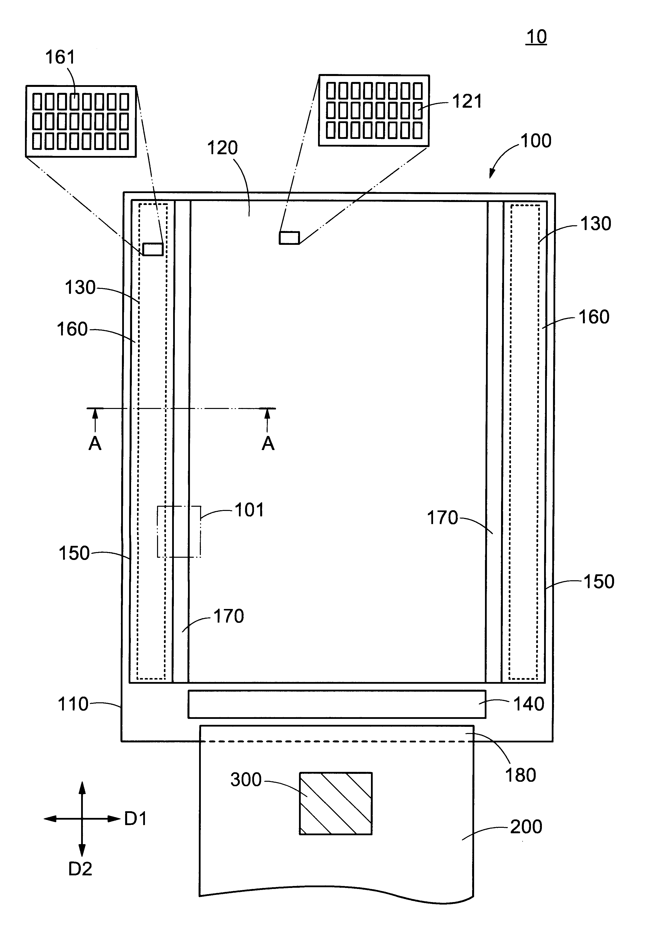
図1は、本発明の第1実施形態の表示装置10の構成を示す平面図である。図2は、本発明の第1実施形態の表示パネル100における接続部170の近傍の構成を示す拡大断面図である。具体的には、図2は、図1に示す表示パネル100をA-A線で切断した断面図に相当する。図3は、本発明の第1実施形態の表示パネル100における接続部170の近傍の構成を示す拡大平面図である。具体的には、図3は、図1に示す表示パネル100において、枠線101で囲まれた範囲を拡大した平面図に相当する。
<First Embodiment>
[Display device configuration]
FIG. 1 is a plan view showing the configuration of the display device 10 according to the first embodiment of the present invention. FIG. 2 is an enlarged cross-sectional view showing a configuration in the vicinity of the connection portion 170 in the display panel 100 of the first embodiment of the present invention. Specifically, FIG. 2 corresponds to a cross-sectional view of the display panel 100 shown in FIG. 1 cut along the line AA. FIG. 3 is an enlarged plan view showing a configuration in the vicinity of the connection portion 170 in the display panel 100 of the first embodiment of the present invention. Specifically, FIG. 3 corresponds to a plan view of the display panel 100 shown in FIG. 1 in which the range surrounded by the frame line 101 is enlarged.

図1に示すように、表示装置10は、表示パネル100、フレキシブルプリント回路基板200(FPC200)、および集積回路300を有する。表示パネル100は、画像を表示する表示デバイスである。フレキシブルプリント回路基板200は、図示しない外部装置から伝達された映像信号または制御信号を、表示パネル100に入力する配線群として機能する。集積回路300は、映像信号に対して所定の信号処理を行ったり、表示制御に必要な制御信号を生成したりする信号処理回路である。集積回路300への信号の入力及び出力は、フレキシブルプリント回路基板200に設けられた配線を介して行われる。 As shown in FIG. 1, the display device 10 includes a display panel 100, a flexible printed circuit board 200 (FPC200), and an integrated circuit 300. The display panel 100 is a display device for displaying an image. The flexible printed circuit board 200 functions as a wiring group for inputting a video signal or a control signal transmitted from an external device (not shown) to the display panel 100. The integrated circuit 300 is a signal processing circuit that performs predetermined signal processing on a video signal and generates a control signal necessary for display control. The input and output of the signal to the integrated circuit 300 are performed via the wiring provided on the flexible printed circuit board 200.

図1及び図2に示すように、表示パネル100は、第1基板110、第1画素部120、ゲート駆動回路130、データ駆動回路140、第2基板150、第2画素部160、接続部170、および端子部180を含む。ただし、これらの要素は一例であり、一部の要素については省略することが可能である。例えば、集積回路300がデータ駆動回路140と同等の機能を有していれば、データ駆動回路140を省略することが可能である。 As shown in FIGS. 1 and 2, the display panel 100 includes a first substrate 110, a first pixel unit 120, a gate drive circuit 130, a data drive circuit 140, a second substrate 150, a second pixel unit 160, and a connection unit 170. , And the terminal portion 180. However, these elements are examples, and some elements can be omitted. For example, if the integrated circuit 300 has the same function as the data drive circuit 140, the data drive circuit 140 can be omitted.

第1基板110は、第1画素部120、ゲート駆動回路130及びデータ駆動回路140を支持する支持基板として機能する。第1基板110としては、ガラス基板、樹脂基板、セラミック基板、半導体基板、金属基板等を用いることができる。本実施形態では、第1基板110としてガラス基板を用いる。第1基板110として樹脂基板を用いた場合、表示パネル100に可撓性を与えることができる。 The first substrate 110 functions as a support substrate that supports the first pixel unit 120, the gate drive circuit 130, and the data drive circuit 140. As the first substrate 110, a glass substrate, a resin substrate, a ceramic substrate, a semiconductor substrate, a metal substrate, or the like can be used. In this embodiment, a glass substrate is used as the first substrate 110. When a resin substrate is used as the first substrate 110, the display panel 100 can be provided with flexibility.

第1画素部120は、行方向(D1方向)および列方向(D2方向)に配置された複数の第1画素121を有する。本実施形態では、第1画素121は、赤、緑、青または白のいずれかの色に対応する画素である。複数の第1画素121は、それぞれ第1発光素子121aを含む。第1発光素子121aは、例えばLED素子である。つまり、第1発光素子121aは、赤色、緑色、青色または白色のいずれかに発光するLED素子である。図2に示すように、各第1発光素子121aは、接続電極121bを介して第1画素121ごとに配置された画素回路121cに接続される。 The first pixel unit 120 has a plurality of first pixels 121 arranged in the row direction (D1 direction) and the column direction (D2 direction). In the present embodiment, the first pixel 121 is a pixel corresponding to any one of red, green, blue, and white. Each of the plurality of first pixels 121 includes a first light emitting element 121a. The first light emitting element 121a is, for example, an LED element. That is, the first light emitting element 121a is an LED element that emits light in any of red, green, blue, and white. As shown in FIG. 2, each first light emitting element 121a is connected to a pixel circuit 121c arranged for each first pixel 121 via a connection electrode 121b.

図1に示すように、ゲート駆動回路130及びデータ駆動回路140は、第1画素部120に隣接して配置される。ゲート駆動回路130は、第1画素部120及び第2画素部160に延在するゲート信号線に対してゲート信号を供給する。データ駆動回路140は、第1画素部120及び第2画素部160に延在するデータ信号線に対してデータ信号を供給する。本実施形態では、第1画素部120に隣接して2つのゲート駆動回路130を配置する例を示したが、この例に限らず、ゲート駆動回路130は、1つであってもよい。 As shown in FIG. 1, the gate drive circuit 130 and the data drive circuit 140 are arranged adjacent to the first pixel unit 120. The gate drive circuit 130 supplies a gate signal to the gate signal line extending to the first pixel unit 120 and the second pixel unit 160. The data drive circuit 140 supplies a data signal to the data signal line extending to the first pixel unit 120 and the second pixel unit 160. In the present embodiment, an example in which two gate drive circuits 130 are arranged adjacent to the first pixel unit 120 is shown, but the present invention is not limited to this example, and the number of gate drive circuits 130 may be one.

第2画素部160は、第1画素部120と同様に、行方向(D1方向)および列方向(D2方向)に配置された複数の第2画素161を有する。本実施形態では、第2画素161は、赤、緑、青または白のいずれかの色に対応する画素である。複数の第2画素161は、それぞれ第2発光素子161aを含む。第2発光素子161aは、例えばLED素子である。つまり、第2発光素子161aは、赤色、緑色、青色または白色のいずれかに発光するLED素子である。図2に示すように、各第2発光素子161aは、接続電極161bを介して第2画素161ごとに配置された画素回路161cに接続される。 The second pixel unit 160 has a plurality of second pixels 161 arranged in the row direction (D1 direction) and the column direction (D2 direction), similarly to the first pixel unit 120. In the present embodiment, the second pixel 161 is a pixel corresponding to any one of red, green, blue, and white. Each of the plurality of second pixels 161 includes a second light emitting element 161a. The second light emitting element 161a is, for example, an LED element. That is, the second light emitting element 161a is an LED element that emits light in any of red, green, blue, and white. As shown in FIG. 2, each second light emitting element 161a is connected to a pixel circuit 161c arranged for each second pixel 161 via a connection electrode 161b.

本実施形態において、第2画素部160は、ゲート駆動回路130の上に配置される。すなわち、図1に示すように、第2画素部160は、平面視においてゲート駆動回路130に重畳して配置される。本実施形態では、ゲート駆動回路130が第1画素部120を挟むように配置されるため、2つの第2画素部160が、第1画素部120を挟むように配置される。第2画素部160の面積は、第1画素部120の面積よりも小さい。しかしながら、ゲート駆動回路130に重畳するように第2画素部160を配置することにより、第1画素部120に加え、ゲート駆動回路130が配置される周辺領域でも画像を表示することが可能となる。 In the present embodiment, the second pixel unit 160 is arranged on the gate drive circuit 130. That is, as shown in FIG. 1, the second pixel unit 160 is arranged so as to be superimposed on the gate drive circuit 130 in a plan view. In the present embodiment, since the gate drive circuit 130 is arranged so as to sandwich the first pixel unit 120, the two second pixel units 160 are arranged so as to sandwich the first pixel unit 120. The area of the second pixel portion 160 is smaller than the area of the first pixel portion 120. However, by arranging the second pixel unit 160 so as to overlap the gate drive circuit 130, it is possible to display an image not only in the first pixel unit 120 but also in the peripheral region where the gate drive circuit 130 is arranged. ..

本実施形態では、第2画素部160は、第2基板150に支持される。つまり、第2基板150は、第2画素部160の支持基板として機能する。第2基板150は、接着層190を用いてゲート駆動回路130の上に接着される。つまり、接着層190は、ゲート駆動回路130と第2画素部160との間に配置される。本実施形態では、接着層190の中には、スペーサ191が配置される。スペーサ191は、第1基板110またはゲート駆動回路130との間の間隔を保持する役割を有する。ただし、この例に限らず、接着層190を用いて間隔を保持することにより、スペーサ191を省略することも可能である。 In this embodiment, the second pixel portion 160 is supported by the second substrate 150. That is, the second substrate 150 functions as a support substrate for the second pixel portion 160. The second substrate 150 is bonded onto the gate drive circuit 130 using the adhesive layer 190. That is, the adhesive layer 190 is arranged between the gate drive circuit 130 and the second pixel portion 160. In the present embodiment, the spacer 191 is arranged in the adhesive layer 190. The spacer 191 has a role of maintaining a space between the first substrate 110 and the gate drive circuit 130. However, the present invention is not limited to this example, and the spacer 191 can be omitted by using the adhesive layer 190 to maintain the space.

さらに、本実施形態では、ゲート駆動回路130と第2画素部160との間に、カップリングによるノイズを低減するためのシールド層135を配置する。シールド層135としては、金属材料または金属酸化物材料で構成される層を用いることができる。本実施形態では、第1画素部120における接続電極121bの形成と同時にシールド層135を形成するため、シールド層135と接続電極121bとは同一の金属材料で構成される。ただし、この例に限らず、シールド層135は、画素回路121cを形成する過程において使用される他の金属材料または金属酸化物材料で構成される導電層で構成されてもよい。シールド層135は、例えばカソード電源線などと電気的に接続し、固定電位に保持することが好ましい。また、シールド層135が遮光性の金属材料により形成される場合、第2発光素子161aからゲート駆動回路130へ向かう光を遮光することができる。これにより、第2発光素子161aの光が照射されることによりゲート駆動回路130が誤作動を起こすなどの不具合を抑制することができる。 Further, in the present embodiment, a shield layer 135 for reducing noise due to coupling is arranged between the gate drive circuit 130 and the second pixel unit 160. As the shield layer 135, a layer made of a metal material or a metal oxide material can be used. In the present embodiment, since the shield layer 135 is formed at the same time as the formation of the connection electrode 121b in the first pixel portion 120, the shield layer 135 and the connection electrode 121b are made of the same metal material. However, not limited to this example, the shield layer 135 may be composed of a conductive layer made of another metal material or metal oxide material used in the process of forming the pixel circuit 121c. The shield layer 135 is preferably electrically connected to, for example, a cathode power line and held at a fixed potential. Further, when the shield layer 135 is formed of a light-shielding metal material, the light directed from the second light emitting element 161a to the gate drive circuit 130 can be shielded. As a result, it is possible to suppress problems such as malfunction of the gate drive circuit 130 due to irradiation of the light of the second light emitting element 161a.

また、本実施形態において、第2基板150の厚さは、第1基板110の厚さよりも薄いことが望ましい。例えば、第2基板150の厚さは、第1基板110の厚さの1/5以下であることが好ましい。第2基板150の厚さを相対的に第1基板110の厚さよりも薄くすることにより、第2基板150及び第2画素部160によって形成される、第1画素部120と第2画素部160との間の段差を目立たなくすることができる。 Further, in the present embodiment, it is desirable that the thickness of the second substrate 150 is thinner than the thickness of the first substrate 110. For example, the thickness of the second substrate 150 is preferably 1/5 or less of the thickness of the first substrate 110. The first pixel portion 120 and the second pixel portion 160 formed by the second substrate 150 and the second pixel portion 160 by making the thickness of the second substrate 150 relatively thinner than the thickness of the first substrate 110. The step between the and can be made inconspicuous.

第2画素部160は、接続部170を介してゲート駆動回路130と電気的に接続される。また、第2画素部160は、接続部170を介して第1画素部120と電気的に接続される。ゲート駆動回路130から出力されたゲート信号は、第1画素部120及び第2画素部160の両方に伝達される。 The second pixel unit 160 is electrically connected to the gate drive circuit 130 via the connection unit 170. Further, the second pixel unit 160 is electrically connected to the first pixel unit 120 via the connection unit 170. The gate signal output from the gate drive circuit 130 is transmitted to both the first pixel unit 120 and the second pixel unit 160.

図2及び図3に示すように、接続部170は、第1パッド171、第2パッド172及び導電部材173を含む。第1パッド171は、第1画素部120とゲート駆動回路130との間に配置された電極である。第2パッド172は、第2画素部160に隣接して配置された電極である。導電部材173は、第1パッド171と第2パッド172とを電気的に接続する。本実施形態では、導電部材173として、樹脂材料にカーボンブラック等の黒色の導電性材料を含有させた部材を用いる。 As shown in FIGS. 2 and 3, the connecting portion 170 includes a first pad 171 and a second pad 172 and a conductive member 173. The first pad 171 is an electrode arranged between the first pixel unit 120 and the gate drive circuit 130. The second pad 172 is an electrode arranged adjacent to the second pixel portion 160. The conductive member 173 electrically connects the first pad 171 and the second pad 172. In the present embodiment, as the conductive member 173, a member in which a black conductive material such as carbon black is contained in a resin material is used.

図2に示すように、導電部材173は、D2方向が長手方向となるように、第2基板150(厳密には、第2基板150及び接着層190)の側面に配置される。また、図3に示すように、導電部材173は、第1画素121と第2画素161との間に配置される。したがって、導電部材173として黒色の部材を用いた場合、第2発光素子161aから横方向(D1方向)に出射された光が、第2基板150の側面を介して第1画素部120へ進行することを抑制することができる。同様に、導電部材173として黒色の部材を用いた場合、第1発光素子121aから横方向(D1方向)に出射された光が、第2基板150の側面を介して第2画素部130へ進行することを抑制することができる。 As shown in FIG. 2, the conductive member 173 is arranged on the side surface of the second substrate 150 (strictly speaking, the second substrate 150 and the adhesive layer 190) so that the D2 direction is the longitudinal direction. Further, as shown in FIG. 3, the conductive member 173 is arranged between the first pixel 121 and the second pixel 161. Therefore, when a black member is used as the conductive member 173, the light emitted from the second light emitting element 161a in the lateral direction (D1 direction) travels to the first pixel portion 120 via the side surface of the second substrate 150. It can be suppressed. Similarly, when a black member is used as the conductive member 173, the light emitted from the first light emitting element 121a in the lateral direction (D1 direction) travels to the second pixel portion 130 via the side surface of the second substrate 150. Can be suppressed.

図3に示すように、第1画素121のそれぞれに電気的に接続された第1ゲート信号線131は、第1パッド171のそれぞれと接続される。第2画素161のそれぞれに電気的に接続された第2ゲート信号線132は、第2パッド172のそれぞれと接続される。すなわち、本実施形態の表示装置10において、各第1ゲート信号線131と各第2ゲート信号線132とは、接続部170を介して1対1に対応して電気的に接続される。具体的には、複数の第1ゲート信号線131におけるN(Nは、自然数)番目のゲート信号線と複数の第2ゲート信号線132におけるN(Nは、自然数)番目のゲート信号線とは、互いに電気的に接続される。 As shown in FIG. 3, the first gate signal line 131 electrically connected to each of the first pixels 121 is connected to each of the first pads 171. The second gate signal line 132 electrically connected to each of the second pixels 161 is connected to each of the second pads 172. That is, in the display device 10 of the present embodiment, each first gate signal line 131 and each second gate signal line 132 are electrically connected one-to-one via a connecting portion 170. Specifically, what is the N (N is a natural number) th gate signal line in the plurality of first gate signal lines 131 and the N (N is a natural number) th gate signal line in the plurality of second gate signal lines 132? , Electrically connected to each other.

以上説明したとおり、本実施形態の表示装置10は、第1画素部120に加え、ゲート駆動回路130に重畳して配置された第2画素部160も画像表示領域として機能させることができる。すなわち、本実施形態の表示装置10は、デッドスペースであった周辺領域を、表示領域として有効に活用することができる。 As described above, in the display device 10 of the present embodiment, in addition to the first pixel unit 120, the second pixel unit 160 arranged superimposed on the gate drive circuit 130 can also function as an image display area. That is, the display device 10 of the present embodiment can effectively utilize the peripheral area that was the dead space as the display area.

[表示パネルの回路構成]
図4は、本発明の第1実施形態の表示パネル100の回路構成を示すブロック図である。ただし、図4は、説明を簡単にするために、第2画素部160及び接続部170については図示を省略している。
[Display panel circuit configuration]
FIG. 4 is a block diagram showing a circuit configuration of the display panel 100 according to the first embodiment of the present invention. However, in FIG. 4, for the sake of simplicity, the second pixel portion 160 and the connection portion 170 are not shown.

第1画素部120に対応する領域には、複数の画素回路121cが配置される。各画素回路121cのそれぞれは、各第1発光素子121aを発光させるための回路である。各画素回路121cは、各第1画素121に対応して配置される。すなわち、第1画素部120には、複数の画素回路121cが、行方向(D1方向)および列方向(D2方向)に配置される。第1画素部120に対して行方向(D1方向)に隣接する位置には、ゲート駆動回路130が配置される。第1画素部120に対して列方向(D2方向)に隣接する位置には、データ駆動回路140が配置される。 A plurality of pixel circuits 121c are arranged in the area corresponding to the first pixel unit 120. Each of the pixel circuits 121c is a circuit for causing each first light emitting element 121a to emit light. Each pixel circuit 121c is arranged corresponding to each first pixel 121. That is, a plurality of pixel circuits 121c are arranged in the first pixel unit 120 in the row direction (D1 direction) and the column direction (D2 direction). The gate drive circuit 130 is arranged at a position adjacent to the row direction (D1 direction) with respect to the first pixel unit 120. The data drive circuit 140 is arranged at a position adjacent to the first pixel unit 120 in the column direction (D2 direction).

ゲート駆動回路130には、複数の第1ゲート信号線131が接続される。データ駆動回路140には、複数の第1データ信号線141が接続される。各第1ゲート信号線131及び各第1データ信号線141は、第1画素部120に延在する。各画素回路121cは、第1ゲート信号線131と第1データ信号線141とが交差する位置に設けられ、第1ゲート信号線131及び第1データ信号線141に電気的に接続される。図4では、説明を簡単にするため、信号線として、第1ゲート信号線131及び第1データ信号線141のみを示しているが、実際には、画素回路121cの構成に応じて、他の信号線が設けられる。 A plurality of first gate signal lines 131 are connected to the gate drive circuit 130. A plurality of first data signal lines 141 are connected to the data drive circuit 140. Each first gate signal line 131 and each first data signal line 141 extend to the first pixel unit 120. Each pixel circuit 121c is provided at a position where the first gate signal line 131 and the first data signal line 141 intersect, and is electrically connected to the first gate signal line 131 and the first data signal line 141. In FIG. 4, for the sake of simplicity, only the first gate signal line 131 and the first data signal line 141 are shown as signal lines, but in reality, other signals may be used depending on the configuration of the pixel circuit 121c. A signal line is provided.

端子部180は、接続配線181を介してゲート駆動回路130に電気的に接続され、接続配線182を介してデータ駆動回路140に電気的に接続される。図1を用いて説明したように、端子部180には、フレキシブルプリント回路基板200が接続される。したがって、フレキシブルプリント回路基板200を介して入力された制御信号及び映像信号は、接続配線181及び182を介してゲート駆動回路130またはデータ駆動回路140に入力される。 The terminal portion 180 is electrically connected to the gate drive circuit 130 via the connection wiring 181 and electrically connected to the data drive circuit 140 via the connection wiring 182. As described with reference to FIG. 1, a flexible printed circuit board 200 is connected to the terminal portion 180. Therefore, the control signal and the video signal input via the flexible printed circuit board 200 are input to the gate drive circuit 130 or the data drive circuit 140 via the connection wirings 181 and 182.

ここで、図4に示す画素回路121cの具体的な回路構成について説明する。図5は、本発明の第1実施形態の表示パネル100における画素回路121cの構成を示す回路図である。画素回路121cは、第1ゲート信号線131の一部、第1データ信号線141の一部、アノード電源線133の一部、カソード電源線134の一部、選択トランジスタ123、駆動トランジスタ124、及び保持容量125を含む。実際には、画素回路121cにおける駆動トランジスタ124とカソード電源線134との間に第1発光素子121aが接続される。ただし、図5において、第1発光素子121aは、画素回路121cに接続される素子であり、画素回路121cを構成する要素ではないため、第1発光素子121aは、点線で図示されている。図5に示した画素回路121cは、一例にすぎず、他の回路構成であってもよい。 Here, a specific circuit configuration of the pixel circuit 121c shown in FIG. 4 will be described. FIG. 5 is a circuit diagram showing the configuration of the pixel circuit 121c in the display panel 100 of the first embodiment of the present invention. The pixel circuit 121c includes a part of the first gate signal line 131, a part of the first data signal line 141, a part of the anode power supply line 133, a part of the cathode power supply line 134, a selection transistor 123, a drive transistor 124, and the like. Includes holding capacity 125. Actually, the first light emitting element 121a is connected between the drive transistor 124 and the cathode power line 134 in the pixel circuit 121c. However, in FIG. 5, since the first light emitting element 121a is an element connected to the pixel circuit 121c and is not an element constituting the pixel circuit 121c, the first light emitting element 121a is shown by a dotted line. The pixel circuit 121c shown in FIG. 5 is merely an example, and may have another circuit configuration.

図5に示すように、選択トランジスタ123のゲート端子は、第1ゲート信号線131に接続される。選択トランジスタ123のソース端子及びドレイン端子は、それぞれ第1データ信号線141及び駆動トランジスタ124のゲート端子に接続される。ただし、選択トランジスタ123のソース端子及びドレイン端子は、選択トランジスタ123のソース-ドレイン間の電位差に応じて、互いに入れ替わる場合がある。 As shown in FIG. 5, the gate terminal of the selection transistor 123 is connected to the first gate signal line 131. The source terminal and drain terminal of the selection transistor 123 are connected to the gate terminal of the first data signal line 141 and the drive transistor 124, respectively. However, the source terminal and the drain terminal of the selection transistor 123 may be interchanged with each other depending on the potential difference between the source and drain of the selection transistor 123.

本実施形態では、駆動トランジスタ124はNチャネル型トランジスタである。したがって、駆動トランジスタ124のソース端子及びドレイン端子は、それぞれ第1発光素子121a及びアノード電源線133に接続される。駆動トランジスタ124のゲート端子とソース端子との間には保持容量125が接続される。すなわち、保持容量125は、選択トランジスタ123のドレイン端子にも接続される。第1発光素子121aのアノード端子は、駆動トランジスタ124を介してアノード電源線133に接続される。第1発光素子121aのカソード端子は、カソード電源線134に接続される。 In this embodiment, the drive transistor 124 is an N-channel transistor. Therefore, the source terminal and the drain terminal of the drive transistor 124 are connected to the first light emitting element 121a and the anode power supply line 133, respectively. A holding capacity 125 is connected between the gate terminal and the source terminal of the drive transistor 124. That is, the holding capacity 125 is also connected to the drain terminal of the selection transistor 123. The anode terminal of the first light emitting element 121a is connected to the anode power supply line 133 via the drive transistor 124. The cathode terminal of the first light emitting element 121a is connected to the cathode power supply line 134.

第1データ信号線141には、第1発光素子121aの発光強度を決めるデータ信号(諧調信号)が供給される。データ信号は、表示する画像に応じた信号であるため、画像信号または映像信号とも呼ばれる。第1ゲート信号線131には、データ信号を書き込む選択トランジスタ123を選択するためのゲート信号が供給される。選択トランジスタ123がオン状態になると、第1データ信号線141から入力されたデータ信号が保持容量125に保持される。その後、駆動トランジスタ124がオン状態になると、データ信号に応じた駆動電流が駆動トランジスタ124のドレイン端子とソース端子との間を流れる。駆動トランジスタ124のソース端子から出力された駆動電流が第1発光素子121aに入力されると、第1発光素子121aがデータ信号に応じた発光強度で発光する。 A data signal (tone signal) that determines the emission intensity of the first light emitting element 121a is supplied to the first data signal line 141. Since the data signal is a signal corresponding to the image to be displayed, it is also called an image signal or a video signal. A gate signal for selecting a selection transistor 123 for writing a data signal is supplied to the first gate signal line 131. When the selection transistor 123 is turned on, the data signal input from the first data signal line 141 is held in the holding capacity 125. After that, when the drive transistor 124 is turned on, a drive current corresponding to the data signal flows between the drain terminal and the source terminal of the drive transistor 124. When the drive current output from the source terminal of the drive transistor 124 is input to the first light emitting element 121a, the first light emitting element 121a emits light with a light emitting intensity corresponding to the data signal.

前述したように、本実施形態の表示装置10は、ゲート駆動回路130の上方に、複数の第2画素161を有する第2画素部160が配置される。各画素回路161cは、前述の画素回路121cと同様の回路構成(すなわち、図5に示した回路構成)を有している。したがって、本実施形態では、第1画素121に加えて、第2画素161に対してゲート信号及びデータ信号を供給する必要がある。 As described above, in the display device 10 of the present embodiment, the second pixel unit 160 having a plurality of second pixels 161 is arranged above the gate drive circuit 130. Each pixel circuit 161c has the same circuit configuration as the pixel circuit 121c described above (that is, the circuit configuration shown in FIG. 5). Therefore, in the present embodiment, it is necessary to supply the gate signal and the data signal to the second pixel 161 in addition to the first pixel 121.

図6は、本発明の第1実施形態の表示パネル100における接続部170の近傍の回路構成を示すブロック図である。具体的には、図6は、第2画素161の画素回路161cとゲート駆動回路130との接続関係を示している。図6に示すように、ゲート駆動回路130に接続された第1ゲート信号線131は、導電部材173を介して第2ゲート信号線132と電気的に接続される。したがって、例えば、ゲート駆動回路130からN番目の第1ゲート信号線131に対して出力されたゲート信号は、第1ゲート信号線131に接続された第2ゲート信号線132にも伝達される。つまり、N番目の第1ゲート信号線131に接続された複数の第1画素121とN番目の第2ゲート信号線132に接続された複数の第2画素161とは、同じ行に位置する画素として制御される。このように、本実施形態では、ゲート駆動回路130が、第1画素部120及び第2画素部160の両方に対してゲート信号を供給する。 FIG. 6 is a block diagram showing a circuit configuration in the vicinity of the connection portion 170 in the display panel 100 of the first embodiment of the present invention. Specifically, FIG. 6 shows the connection relationship between the pixel circuit 161c of the second pixel 161 and the gate drive circuit 130. As shown in FIG. 6, the first gate signal line 131 connected to the gate drive circuit 130 is electrically connected to the second gate signal line 132 via the conductive member 173. Therefore, for example, the gate signal output from the gate drive circuit 130 to the Nth first gate signal line 131 is also transmitted to the second gate signal line 132 connected to the first gate signal line 131. That is, the plurality of first pixels 121 connected to the Nth first gate signal line 131 and the plurality of second pixels 161 connected to the Nth second gate signal line 132 are pixels located in the same row. Is controlled as. As described above, in the present embodiment, the gate drive circuit 130 supplies the gate signal to both the first pixel unit 120 and the second pixel unit 160.

図7は、本発明の第1実施形態の表示パネル100における接続部170の近傍の回路構成を示すブロック図である。具体的には、図7は、第2画素161の画素回路161cとデータ駆動回路140との接続関係を示している。図7に示すように、データ駆動回路140に接続された第1データ信号線141の一部は、第1画素121の画素回路121cに接続される。他方、第1データ信号線141の他の一部は、導電部材173を介して第2データ信号線142と電気的に接続される。第2データ信号線142は、第2画素161の画素回路161cに接続される。このように、本実施形態では、データ駆動回路140が、第1画素部120及び第2画素部160の両方に対してデータ信号を供給する。 FIG. 7 is a block diagram showing a circuit configuration in the vicinity of the connection portion 170 in the display panel 100 of the first embodiment of the present invention. Specifically, FIG. 7 shows the connection relationship between the pixel circuit 161c of the second pixel 161 and the data drive circuit 140. As shown in FIG. 7, a part of the first data signal line 141 connected to the data drive circuit 140 is connected to the pixel circuit 121c of the first pixel 121. On the other hand, the other part of the first data signal line 141 is electrically connected to the second data signal line 142 via the conductive member 173. The second data signal line 142 is connected to the pixel circuit 161c of the second pixel 161. As described above, in the present embodiment, the data drive circuit 140 supplies the data signal to both the first pixel unit 120 and the second pixel unit 160.

[画素の断面構造]
図8は、本発明の第1実施形態の表示パネル100における画素の構成を示す断面図である。本実施形態では、表示パネル100の画素構造について、第1画素121を例示して説明する。第2画素161の断面構造は、第1画素121の断面構造と同じであるため、第2画素161についての説明は省略する。また、図5に示したように、第1画素121には、複数のトランジスタを用いた画素回路121cが配置されるが、説明を簡単にするため、一部の要素についての説明を省略する。
[Cross-sectional structure of pixels]
FIG. 8 is a cross-sectional view showing the configuration of pixels in the display panel 100 according to the first embodiment of the present invention. In the present embodiment, the pixel structure of the display panel 100 will be described by exemplifying the first pixel 121. Since the cross-sectional structure of the second pixel 161 is the same as the cross-sectional structure of the first pixel 121, the description of the second pixel 161 will be omitted. Further, as shown in FIG. 5, a pixel circuit 121c using a plurality of transistors is arranged in the first pixel 121, but the description of some elements will be omitted for the sake of simplicity.

第1基板110の上には、ベース層11が設けられる。ベース層11は、酸化シリコン層、窒化シリコン層、または、それらを積層した絶縁層である。ベース層11は、第1基板110からアルカリ成分等が侵入することを防ぐバリア層として機能する。ベース層11の上には、駆動トランジスタ124(図5参照)が設けられる。 A base layer 11 is provided on the first substrate 110. The base layer 11 is a silicon oxide layer, a silicon nitride layer, or an insulating layer obtained by laminating them. The base layer 11 functions as a barrier layer for preventing the intrusion of alkaline components and the like from the first substrate 110. A drive transistor 124 (see FIG. 5) is provided on the base layer 11.

駆動トランジスタ124は、半導体層12、ゲート絶縁層13およびゲート電極14を含む。半導体層12には、絶縁層15を介してソース電極16およびドレイン電極17が接続される。ソース電極16及びドレイン電極17は、それぞれ駆動トランジスタ124のソース端子及びドレイン端子として機能する。図示は省略するが、ゲート電極14は、図5に示したように選択トランジスタ123のドレイン端子に接続される。 The drive transistor 124 includes a semiconductor layer 12, a gate insulating layer 13, and a gate electrode 14. A source electrode 16 and a drain electrode 17 are connected to the semiconductor layer 12 via an insulating layer 15. The source electrode 16 and the drain electrode 17 function as a source terminal and a drain terminal of the drive transistor 124, respectively. Although not shown, the gate electrode 14 is connected to the drain terminal of the selection transistor 123 as shown in FIG.

ソース電極16およびドレイン電極17と同一の層には、配線18が設けられている。配線18は、図5に示したアノード電源線133として機能する。そのため、ソース電極16および配線18は、平坦化層19の上に設けられた接続配線20によって電気的に接続される。平坦化層19は、ポリイミド、アクリル等の樹脂材料を用いた透明な樹脂層である。接続配線20は、ITO(Indium Tin Oxide)などの金属酸化物材料を用いた透明導電層である。ただし、この例に限らず、接続配線20として、その他の金属材料を用いることもできる。 Wiring 18 is provided on the same layer as the source electrode 16 and the drain electrode 17. The wiring 18 functions as the anode power line 133 shown in FIG. Therefore, the source electrode 16 and the wiring 18 are electrically connected by the connection wiring 20 provided on the flattening layer 19. The flattening layer 19 is a transparent resin layer using a resin material such as polyimide or acrylic. The connection wiring 20 is a transparent conductive layer using a metal oxide material such as ITO (Indium Tin Oxide). However, the present invention is not limited to this example, and other metal materials may be used as the connection wiring 20.

接続配線20の上には、窒化シリコン等で構成された絶縁層21が設けられる。絶縁層21の上には、アノード電極22およびカソード電極23が設けられる。本実施形態において、アノード電極22およびカソード電極23は、ITOなどの金属酸化物材料を用いた透明導電層である。アノード電極22は、平坦化層19および絶縁層21に設けられた開口を介してドレイン電極17に接続される。 An insulating layer 21 made of silicon nitride or the like is provided on the connection wiring 20. An anode electrode 22 and a cathode electrode 23 are provided on the insulating layer 21. In the present embodiment, the anode electrode 22 and the cathode electrode 23 are transparent conductive layers using a metal oxide material such as ITO. The anode electrode 22 is connected to the drain electrode 17 via the openings provided in the flattening layer 19 and the insulating layer 21.

アノード電極22およびカソード電極23は、それぞれ平坦化層24を介して実装パッド25aおよび25bに接続される。実装パッド25aおよび25bは、例えば、タンタル、タングステン等の金属材料で構成される。実装パッド25aおよび25bの上には、それぞれ接続電極26aおよび26bが設けられる。本実施形態では、接続電極26aおよび26bとして、錫(Sn)で構成される電極を配置する。図8に示す接続電極26a及び26bは、図2に示した接続電極121bに対応する。 The anode electrode 22 and the cathode electrode 23 are connected to the mounting pads 25a and 25b via the flattening layer 24, respectively. The mounting pads 25a and 25b are made of a metal material such as tantalum or tungsten. Connection electrodes 26a and 26b are provided on the mounting pads 25a and 25b, respectively. In the present embodiment, electrodes composed of tin (Sn) are arranged as the connection electrodes 26a and 26b. The connection electrodes 26a and 26b shown in FIG. 8 correspond to the connection electrodes 121b shown in FIG.

接続電極26aおよび26bには、それぞれ第1発光素子121aの端子電極27aおよび27bが接合される。本実施形態では、端子電極27aおよび27bは、金(Au)で構成される電極である。端子電極27aおよび27bは、銀(Ag)で構成されてもよい。 The terminal electrodes 27a and 27b of the first light emitting element 121a are bonded to the connection electrodes 26a and 26b, respectively. In this embodiment, the terminal electrodes 27a and 27b are electrodes made of gold (Au). The terminal electrodes 27a and 27b may be made of silver (Ag).

第1発光素子121aは、図5に示したように、駆動トランジスタ124のドレイン端子とカソード電源線134との間に接続される。すなわち、第1発光素子121aの端子電極27aは、駆動トランジスタ124のドレイン電極17に接続されたアノード電極22に接続される。第1発光素子121aの端子電極27bは、カソード電極23に接続される。図8では図示を省略しているが、カソード電極23は、図5に示したようにカソード電源線134と電気的に接続される。 As shown in FIG. 5, the first light emitting element 121a is connected between the drain terminal of the drive transistor 124 and the cathode power supply line 134. That is, the terminal electrode 27a of the first light emitting element 121a is connected to the anode electrode 22 connected to the drain electrode 17 of the drive transistor 124. The terminal electrode 27b of the first light emitting element 121a is connected to the cathode electrode 23. Although not shown in FIG. 8, the cathode electrode 23 is electrically connected to the cathode power supply line 134 as shown in FIG.

本実施形態では、第1発光素子121aとして、フリップチップ型のLED素子を用いる例について説明した。フリップチップ型のLED素子は、n型半導体及びp型半導体のそれぞれに接続された端子電極が、同一方向(図8に示す例では、第1基板110に向かう方向)に向かって配置された構造を有している。しかしながら、この例に限られず、第1発光素子121aとして、フェイスアップ型のLED素子を用いることも可能である。フェイスアップ型のLED素子は、支持基板に近い側にアノード電極(もしくはカソード電極)を有し、支持基板から遠い側にカソード電極(もしくはアノード電極)を有する構造を有する。換言すれば、フェイスアップ型のLED素子は、アノード電極とカソード電極との間に半導体層を挟んだ構造を有している。 In this embodiment, an example in which a flip-chip type LED element is used as the first light emitting element 121a has been described. The flip-chip type LED element has a structure in which terminal electrodes connected to each of the n-type semiconductor and the p-type semiconductor are arranged in the same direction (in the example shown in FIG. 8, the direction toward the first substrate 110). have. However, the present invention is not limited to this example, and a face-up type LED element can be used as the first light emitting element 121a. The face-up type LED element has a structure having an anode electrode (or cathode electrode) on the side close to the support substrate and a cathode electrode (or cathode electrode) on the side far from the support substrate. In other words, the face-up type LED element has a structure in which a semiconductor layer is sandwiched between an anode electrode and a cathode electrode.

[表示装置の製造方法]
図9A、図9B、図10A及び図10Bは、本発明の第1実施形態の表示パネル100の製造方法を示す断面図である。
[Manufacturing method of display device]
9A, 9B, 10A and 10B are cross-sectional views showing a method of manufacturing the display panel 100 according to the first embodiment of the present invention.

まず、図9Aに示すように、第1基板110の上に、画素回路121c、第1パッド171及びゲート駆動回路130を形成する。画素回路121c及びゲート駆動回路130は、公知の薄膜形成技術を用いて形成したトランジスタを用いて構成すればよい。図示は省略するが、第1基板110の上には、他にもデータ駆動回路140及び端子部180等が形成される。画素回路121cの上には、接続電極121bが形成される。ゲート駆動回路130の上には、接続電極121bの形成と同時に、シールド層135が形成される。 First, as shown in FIG. 9A, the pixel circuit 121c, the first pad 171 and the gate drive circuit 130 are formed on the first substrate 110. The pixel circuit 121c and the gate drive circuit 130 may be configured by using transistors formed by using a known thin film forming technique. Although not shown, a data drive circuit 140, a terminal portion 180, and the like are also formed on the first substrate 110. A connection electrode 121b is formed on the pixel circuit 121c. A shield layer 135 is formed on the gate drive circuit 130 at the same time as the connection electrode 121b is formed.

次に、図9Bに示すように、各接続電極121bの上に第1発光素子121aが配置される。本実施形態では、各接続電極121bの上に、各第1発光素子121aを載せた状態でレーザー光の照射を行い、接続電極121bと第1発光素子121aの端子電極27a及び27b(図8参照)とを接合する。本実施形態では、接続電極121bの構成材料が錫であり、端子電極27a及び27bの構成材料が金であるため、接合部には錫と金とで構成される共晶合金が形成される。これにより、複数の第1画素121を有する第1画素部120を形成することができる。 Next, as shown in FIG. 9B, the first light emitting element 121a is arranged on each connection electrode 121b. In the present embodiment, laser light is irradiated with each first light emitting element 121a mounted on each connection electrode 121b, and the connection electrodes 121b and the terminal electrodes 27a and 27b of the first light emitting element 121a (see FIG. 8). ) And join. In the present embodiment, since the constituent material of the connection electrode 121b is tin and the constituent materials of the terminal electrodes 27a and 27b are gold, a eutectic alloy composed of tin and gold is formed at the joint portion. As a result, the first pixel unit 120 having a plurality of first pixels 121 can be formed.

次に、図10Aに示すように、第2画素部160及び第2パッド172をゲート駆動回路130の上に接着する。具体的には、ゲート駆動回路130の上に、接着層190を介して第2基板150を接着する。本実施形態では、接着層190として、熱硬化樹脂を用いる。このとき、第1基板110の上において、第1パッド171の少なくとも一部を露出させておく。 Next, as shown in FIG. 10A, the second pixel portion 160 and the second pad 172 are bonded onto the gate drive circuit 130. Specifically, the second substrate 150 is adhered onto the gate drive circuit 130 via the adhesive layer 190. In this embodiment, a thermosetting resin is used as the adhesive layer 190. At this time, at least a part of the first pad 171 is exposed on the first substrate 110.

次に、図10Bに示すように、導電部材173を形成して、第1パッド171と第2パッド172とを電気的に接続する。導電部材173の形成方法に特に制限はないが、導電材料を含む微量な液体を局所的に塗布する方法を用いることが好ましい。このような方法としては、ディスペンサー方式、インクジェット方式、静電塗布方式などの塗布方法が挙げられる。このように、局所的に狙った部分に導電材料を塗布する技術を用いれば、高い自由度で導電部材173を形成することができる。以上の方法により、図2を用いて説明した表示装置10を形成することができる。 Next, as shown in FIG. 10B, the conductive member 173 is formed to electrically connect the first pad 171 and the second pad 172. The method for forming the conductive member 173 is not particularly limited, but it is preferable to use a method in which a trace amount of liquid containing a conductive material is locally applied. Examples of such a method include coating methods such as a dispenser method, an inkjet method, and an electrostatic coating method. As described above, if the technique of applying the conductive material to the locally targeted portion is used, the conductive member 173 can be formed with a high degree of freedom. By the above method, the display device 10 described with reference to FIG. 2 can be formed.

<第2実施形態>
本実施形態では、第1実施形態とは異なる方法でゲート駆動回路130と第2画素部160とを電気的に接続した例について説明する。具体的には、本実施形態の表示パネル100は、接続部170aに含まれる導電部材173aが、第2基板150aを貫通する。本実施形態では、第1実施形態と相違する部分について説明する。本実施形態の説明に用いる図面について、第1実施形態と同一の構成については、同一の符号を付して詳細な説明を省略する。
<Second Embodiment>
In this embodiment, an example in which the gate drive circuit 130 and the second pixel unit 160 are electrically connected by a method different from that of the first embodiment will be described. Specifically, in the display panel 100 of the present embodiment, the conductive member 173a included in the connecting portion 170a penetrates the second substrate 150a. In this embodiment, a part different from the first embodiment will be described. Regarding the drawings used for the description of the present embodiment, the same components as those of the first embodiment are designated by the same reference numerals, and detailed description thereof will be omitted.

図11は、本発明の第2実施形態の表示パネル100aにおける接続部170aの近傍の構成を示す拡大断面図である。図12は、本発明の第2実施形態の表示パネル100aにおける接続部170aの近傍の構成を示す拡大平面図である。図11に示すように、本実施形態の導電部材173aは、第1パッド171と第2パッド172とを電気的に接続する際に、第2基板150a及び接着層190aを貫通する。つまり、導電部材173aは、第2基板150a及び接着層190aのそれぞれに設けられた開口部151及び192を介して第1パッド171及び第2パッド172に接続される。 FIG. 11 is an enlarged cross-sectional view showing a configuration in the vicinity of the connection portion 170a in the display panel 100a according to the second embodiment of the present invention. FIG. 12 is an enlarged plan view showing a configuration in the vicinity of the connection portion 170a in the display panel 100a according to the second embodiment of the present invention. As shown in FIG. 11, the conductive member 173a of the present embodiment penetrates the second substrate 150a and the adhesive layer 190a when the first pad 171 and the second pad 172 are electrically connected. That is, the conductive member 173a is connected to the first pad 171 and the second pad 172 via the openings 151 and 192 provided in the second substrate 150a and the adhesive layer 190a, respectively.

本実施形態では、第2基板150a及び接着層190aは、どちらも樹脂材料で構成される。したがって、接着層190aを用いて第2基板150aを接着した後、例えばレーザー光の照射等により開口部151及び開口部192を形成することができる。開口部151及び開口部192を形成した後、第1実施形態と同様の方法(例えば、ディスペンサー方式など)で導電部材173aを形成すればよい。 In the present embodiment, both the second substrate 150a and the adhesive layer 190a are made of a resin material. Therefore, after the second substrate 150a is adhered using the adhesive layer 190a, the opening 151 and the opening 192 can be formed by, for example, irradiation with a laser beam or the like. After forming the opening 151 and the opening 192, the conductive member 173a may be formed by the same method as in the first embodiment (for example, a dispenser method or the like).

図12に示すように、導電部材173aは、D2方向が長手方向となるように、第1画素121と第2画素161との間に配置される。したがって、導電部材173aとして黒色の部材を用いた場合、第2発光素子161aから横方向(D1方向)に出射された光が、第1画素部120へ進行することを抑制することができる。ただし、導電部材173bが黒色であることは、必須ではない。 As shown in FIG. 12, the conductive member 173a is arranged between the first pixel 121 and the second pixel 161 so that the D2 direction is the longitudinal direction. Therefore, when a black member is used as the conductive member 173a, it is possible to suppress the light emitted from the second light emitting element 161a in the lateral direction (D1 direction) from advancing to the first pixel unit 120. However, it is not essential that the conductive member 173b is black.

<第3実施形態>
本実施形態では、第1実施形態とは異なる方法でゲート駆動回路130と第2画素部160とを電気的に接続した例について説明する。具体的には、本実施形態の表示パネル100は、第1パッド171と第2パッド172とを向かい合わせに配置し、それらの間を導電部材173bにより電気的に接続する。本実施形態では、第1実施形態と相違する部分について説明する。本実施形態の説明に用いる図面について、第1実施形態と同一の構成については、同一の符号を付して詳細な説明を省略する。
<Third Embodiment>
In this embodiment, an example in which the gate drive circuit 130 and the second pixel unit 160 are electrically connected by a method different from that of the first embodiment will be described. Specifically, in the display panel 100 of the present embodiment, the first pad 171 and the second pad 172 are arranged to face each other, and the two pads are electrically connected to each other by a conductive member 173b. In this embodiment, a part different from the first embodiment will be described. Regarding the drawings used for the description of the present embodiment, the same components as those of the first embodiment are designated by the same reference numerals, and detailed description thereof will be omitted.

図13は、本発明の第3実施形態の表示パネル100bにおける接続部170aの近傍の構成を示す拡大断面図である。図14は、本発明の第3実施形態の表示パネル100bにおける接続部170bの近傍の構成を示す拡大平面図である。図13に示すように、本実施形態では、第2基板150及び第2画素部160の位置関係が第1実施形態とは逆である。すなわち、本実施形態の表示パネル100bは、第1パッド171と第2パッド172とが向かい合わせに配置される。そして、第1パッド171と第2パッド172との間には、導電部材173bが配置される。これにより、ゲート駆動回路130と第2画素部160とを電気的に接続することができる。 FIG. 13 is an enlarged cross-sectional view showing a configuration in the vicinity of the connection portion 170a in the display panel 100b according to the third embodiment of the present invention. FIG. 14 is an enlarged plan view showing a configuration in the vicinity of the connection portion 170b in the display panel 100b according to the third embodiment of the present invention. As shown in FIG. 13, in the present embodiment, the positional relationship between the second substrate 150 and the second pixel unit 160 is opposite to that in the first embodiment. That is, in the display panel 100b of the present embodiment, the first pad 171 and the second pad 172 are arranged to face each other. Then, a conductive member 173b is arranged between the first pad 171 and the second pad 172. As a result, the gate drive circuit 130 and the second pixel unit 160 can be electrically connected.

導電部材173bは、第1実施形態及び第2実施形態と同様の方法(例えば、ディスペンサー方式など)で形成することが可能である。本実施形態では、予め第1パッド171の上に導電部材173bを形成しておく。その後、ゲート駆動回路130の上、及び、導電部材173bの周囲に、接着層190を設ける。接着層190を設けたら、第1パッド171の位置と第2パッド172の位置とが重畳するように第1基板110と第2基板150との位置合わせを行う。第1基板110と第2基板150との位置合わせを行った後、接着層190を介して第1基板110と第2基板150とを貼り合わせる。このとき、第1パッド171と第2パッド172とが導電部材173bを介して電気的に接続される。 The conductive member 173b can be formed by the same method as in the first embodiment and the second embodiment (for example, a dispenser method or the like). In the present embodiment, the conductive member 173b is formed on the first pad 171 in advance. After that, the adhesive layer 190 is provided on the gate drive circuit 130 and around the conductive member 173b. After the adhesive layer 190 is provided, the positions of the first substrate 110 and the second substrate 150 are aligned so that the positions of the first pad 171 and the positions of the second pad 172 overlap. After aligning the first substrate 110 and the second substrate 150, the first substrate 110 and the second substrate 150 are bonded together via the adhesive layer 190. At this time, the first pad 171 and the second pad 172 are electrically connected via the conductive member 173b.

図14に示すように、導電部材173bは、D2方向が長手方向となるように、第1画素121と第2画素161との間に配置される。したがって、導電部材173bとして黒色の部材を用いた場合、第2発光素子161aから横方向(D1方向)に出射された光が、第1画素部120へ進行することを抑制することができる。ただし、導電部材173bが黒色であることは、必須ではない。 As shown in FIG. 14, the conductive member 173b is arranged between the first pixel 121 and the second pixel 161 so that the D2 direction is the longitudinal direction. Therefore, when a black member is used as the conductive member 173b, it is possible to suppress the light emitted from the second light emitting element 161a in the lateral direction (D1 direction) from advancing to the first pixel unit 120. However, it is not essential that the conductive member 173b is black.

本実施形態では、第2発光素子161aから出力された光が、第2基板150を通して出射される。すなわち、本実施形態の第2発光素子161aの光出射面は、第1実施形態の第2発光素子161aの光出射面とは逆である。ただし、この例に限られるものではなく、本実施形態は、第1実施形態と同じ構造の第2発光素子161aを用いてもよい。その場合、第2発光素子161aの下方に位置するシールド層135を金属材料で構成することにより、反射部材として利用すればよい。 In the present embodiment, the light output from the second light emitting element 161a is emitted through the second substrate 150. That is, the light emitting surface of the second light emitting element 161a of the present embodiment is opposite to the light emitting surface of the second light emitting element 161a of the first embodiment. However, the present invention is not limited to this example, and the second light emitting element 161a having the same structure as that of the first embodiment may be used in the present embodiment. In that case, the shield layer 135 located below the second light emitting element 161a may be used as a reflective member by being made of a metal material.

<第4実施形態>
本実施形態では、第1実施形態とは異なる第1画素部120c及び第2画素部160cを有する表示パネル100cの例について説明する。具体的には、本実施形態の表示パネル100cは、第1画素部120c及び第2画素部160cに、それぞれ第1遮光層31及び第2遮光層32が設けられている。本実施形態では、第1実施形態と相違する部分について説明する。本実施形態の説明に用いる図面について、第1実施形態と同一の構成については、同一の符号を付して詳細な説明を省略する。
<Fourth Embodiment>
In this embodiment, an example of a display panel 100c having a first pixel unit 120c and a second pixel unit 160c different from the first embodiment will be described. Specifically, in the display panel 100c of the present embodiment, the first pixel unit 120c and the second pixel unit 160c are provided with a first light-shielding layer 31 and a second light-shielding layer 32, respectively. In this embodiment, a part different from the first embodiment will be described. Regarding the drawings used for the description of the present embodiment, the same components as those of the first embodiment are designated by the same reference numerals, and detailed description thereof will be omitted.

図15は、本発明の第4実施形態の表示パネル100cにおける接続部170cの近傍の構成を示す拡大平面図である。図15に示すように、本実施形態の表示パネル100cは、第1画素部120cに第1遮光層31を有する。第1遮光層31は、第1発光素子121aに対応する位置(換言すれば、第1画素121に対応する位置ともいえる)に開口部31aを有する。 FIG. 15 is an enlarged plan view showing a configuration in the vicinity of the connection portion 170c in the display panel 100c according to the fourth embodiment of the present invention. As shown in FIG. 15, the display panel 100c of the present embodiment has a first light-shielding layer 31 in the first pixel unit 120c. The first light-shielding layer 31 has an opening 31a at a position corresponding to the first light emitting element 121a (in other words, a position corresponding to the first pixel 121).

第1遮光層31は、例えば黒色顔料を含む樹脂層を用いることができる。すなわち、第1遮光層31は、絶縁性の黒色部材である。これにより、本実施形態の表示パネル100cは、第1画素部120cにおける第1画素121以外の領域が、光を吸収する領域として機能する。 As the first light-shielding layer 31, for example, a resin layer containing a black pigment can be used. That is, the first light-shielding layer 31 is an insulating black member. As a result, in the display panel 100c of the present embodiment, the region other than the first pixel 121 in the first pixel unit 120c functions as a region for absorbing light.

また、第2画素部160cは、第1画素部120cと同様に、第2遮光層32を有する。第2遮光層32は、第2発光素子161aに対応する位置(換言すれば、第2画素161に対応する位置ともいえる)に開口部32aを有する。この場合においても、第2画素部160cにおける第2画素161以外の領域は、光を吸収する領域として機能する。 Further, the second pixel unit 160c has a second light-shielding layer 32, similarly to the first pixel unit 120c. The second light-shielding layer 32 has an opening 32a at a position corresponding to the second light emitting element 161a (in other words, a position corresponding to the second pixel 161). Even in this case, the region other than the second pixel 161 in the second pixel portion 160c functions as a region for absorbing light.

以上のとおり、本実施形態の表示パネル100cは、第1画素部120c及び第2画素部160cに、光を吸収する第1遮光層31及び第2遮光層32を有する。そのため、第1画素部120c及び第2画素部160cでは、外部から侵入した光を吸収することができる。これにより、第2基板150及び第2画素部160cによって形成される段差を目立たなくすることができる。また、画素以外の領域で反射する光を抑制することにより、画像表示の際、コントラストを向上させることができる。 As described above, the display panel 100c of the present embodiment has a first light-shielding layer 31 and a second light-shielding layer 32 for absorbing light in the first pixel unit 120c and the second pixel unit 160c. Therefore, the first pixel unit 120c and the second pixel unit 160c can absorb the light that has entered from the outside. Thereby, the step formed by the second substrate 150 and the second pixel portion 160c can be made inconspicuous. Further, by suppressing the light reflected in the region other than the pixel, the contrast can be improved at the time of displaying the image.

<第5実施形態>
本実施形態では、第1実施形態とは異なる第2画素部160dを有する表示パネル100dの例について説明する。具体的には、本実施形態の表示パネル100dは、第2画素部160dの一部が湾曲している。本実施形態では、第1実施形態と相違する部分について説明する。本実施形態の説明に用いる図面について、第1実施形態と同一の構成については、同一の符号を付して詳細な説明を省略する。
<Fifth Embodiment>
In this embodiment, an example of a display panel 100d having a second pixel portion 160d different from that of the first embodiment will be described. Specifically, in the display panel 100d of the present embodiment, a part of the second pixel portion 160d is curved. In this embodiment, a part different from the first embodiment will be described. Regarding the drawings used for the description of the present embodiment, the same components as those of the first embodiment are designated by the same reference numerals, and detailed description thereof will be omitted.

図16は、本発明の第5実施形態の表示パネル100dにおける接続部170の近傍の構成を示す拡大断面図である。本実施形態では、第2画素部160dを支持する第2基板150dとして、樹脂材料で構成された基板を用いる。つまり、第2基板150dは、可撓性を有するフレキシブル基板である。したがって、本実施形態では、第2基板150dの可撓性を利用することにより、第2基板150dの一部(具体的には、平面視において、第1基板110と重畳しない部分)を湾曲させることが可能である。 FIG. 16 is an enlarged cross-sectional view showing a configuration in the vicinity of the connection portion 170 in the display panel 100d according to the fifth embodiment of the present invention. In the present embodiment, a substrate made of a resin material is used as the second substrate 150d that supports the second pixel portion 160d. That is, the second substrate 150d is a flexible substrate having flexibility. Therefore, in the present embodiment, by utilizing the flexibility of the second substrate 150d, a part of the second substrate 150d (specifically, a portion that does not overlap with the first substrate 110 in a plan view) is curved. It is possible.

第1実施形態と同様に、第2基板150dの厚さは、第1基板110の厚さよりも薄いことが望ましい。例えば、第2基板150dの厚さは、第1基板110の厚さの1/5以下であることが好ましい。第2基板150dの厚さを相対的に第1基板110の厚さよりも薄くすることにより、第2基板150d及び第2画素部160dによって形成される、第1画素部120と第2画素部160dとの間の段差を目立たなくすることができる。 As in the first embodiment, it is desirable that the thickness of the second substrate 150d is thinner than the thickness of the first substrate 110. For example, the thickness of the second substrate 150d is preferably 1/5 or less of the thickness of the first substrate 110. By making the thickness of the second substrate 150d relatively thinner than the thickness of the first substrate 110, the first pixel portion 120 and the second pixel portion 160d formed by the second substrate 150d and the second pixel portion 160d are formed. The step between the and can be made inconspicuous.

本実施形態の表示パネル100cは、図16に示すように、平面視において、第2基板150dが湾曲しているため、第2基板150dに支持された第2画素部160dも湾曲している。図16には図示されないが、第1実施形態と同様に、表示パネル100dは、第1画素部120を挟むように第2画素部160dを有する。すなわち、本実施形態の表示パネル100cは、ゲート駆動回路130が配置される側の画面端部に湾曲部160daを有し、当該湾曲部160daにも画像を表示することができる。 As shown in FIG. 16, in the display panel 100c of the present embodiment, since the second substrate 150d is curved in a plan view, the second pixel portion 160d supported by the second substrate 150d is also curved. Although not shown in FIG. 16, the display panel 100d has a second pixel portion 160d so as to sandwich the first pixel portion 120, as in the first embodiment. That is, the display panel 100c of the present embodiment has a curved portion 160da at the end of the screen on the side where the gate drive circuit 130 is arranged, and an image can be displayed on the curved portion 160da as well.

<第6実施形態>
本実施形態では、複数の表示パネルを連結した複合画面を有する表示装置の例について説明する。具体的には、本実施形態の表示パネル100eは、第1表示パネル100-1と第2表示パネル100-2とを連結して横長の表示パネル100eを構成している。本実施形態では、第1実施形態と相違する部分について説明する。本実施形態の説明に用いる図面について、第1実施形態と同一の構成については、同一の符号を付して詳細な説明を省略する。
<Sixth Embodiment>
In this embodiment, an example of a display device having a composite screen in which a plurality of display panels are connected will be described. Specifically, the display panel 100e of the present embodiment constitutes a horizontally long display panel 100e by connecting the first display panel 100-1 and the second display panel 100-2. In this embodiment, a part different from the first embodiment will be described. Regarding the drawings used for the description of the present embodiment, the same components as those of the first embodiment are designated by the same reference numerals, and detailed description thereof will be omitted.

図17は、本発明の第6実施形態の表示パネル100eの構成を示す平面図である。図18は、本発明の第6実施形態の表示パネル100eにおける連結部の近傍の構成を示す拡大断面図である。具体的には、図18は、図17に示す表示パネル100eをB-B線で切断した断面図に相当する。 FIG. 17 is a plan view showing the configuration of the display panel 100e according to the sixth embodiment of the present invention. FIG. 18 is an enlarged cross-sectional view showing a configuration in the vicinity of the connecting portion in the display panel 100e according to the sixth embodiment of the present invention. Specifically, FIG. 18 corresponds to a cross-sectional view of the display panel 100e shown in FIG. 17 cut along the line BB.

図17に示すように、本実施形態の表示パネル100eは、第1表示パネル100-1と第2表示パネル100-2とを長辺を向かい合わせて連結した構成を有する。本実施形態において、表示パネル100eは、第1表示パネル100-1と第2表示パネル100-2とに跨って第2画素部160eを有する。すなわち、表示パネル100eは、複数の表示パネル(具体的には、第1表示パネル100-1及び第2表示パネル100-2)で1つの第2画素部160eを共有する構造を有する。ただし、本実施形態では、2枚の表示パネルを連結する例を示したが、この例に限らず、連結する表示パネルの枚数に制限はない。 As shown in FIG. 17, the display panel 100e of the present embodiment has a configuration in which the first display panel 100-1 and the second display panel 100-2 are connected with their long sides facing each other. In the present embodiment, the display panel 100e has a second pixel portion 160e straddling the first display panel 100-1 and the second display panel 100-2. That is, the display panel 100e has a structure in which one second pixel portion 160e is shared by a plurality of display panels (specifically, the first display panel 100-1 and the second display panel 100-2). However, in the present embodiment, an example of connecting two display panels is shown, but the present invention is not limited to this example, and the number of display panels to be connected is not limited.

図18に示すように、第1表示パネル100-1及び第2表示パネル100-2は、それぞれが第1実施形態と同様の構成を有している。第1実施形態と異なる点は、第2画素部160eが、第1表示パネル100-1と第2表示パネル100-2とに跨って設けられている点である。したがって、本実施形態の表示パネル100eは、第1表示パネル100-1と第2表示パネル100-2との連結部においても第2画素部160eによって画像を表示することができる。 As shown in FIG. 18, the first display panel 100-1 and the second display panel 100-2 each have the same configuration as that of the first embodiment. The difference from the first embodiment is that the second pixel unit 160e is provided so as to straddle the first display panel 100-1 and the second display panel 100-2. Therefore, the display panel 100e of the present embodiment can display an image by the second pixel unit 160e even at the connecting portion between the first display panel 100-1 and the second display panel 100-2.

本実施形態の表示パネル100eがさらに第1実施形態と異なる点は、第2表示パネル100-2の接続部170eが第2パッドを有していない点である。すなわち、本実施形態において、第2画素部160eは、ゲート駆動回路130-1と電気的に接続されるものの、ゲート駆動回路130-2とは電気的に接続されない。本実施形態では、第2表示パネル100-2において、接続部170eから第2パッドを省略した例を示したが、これに限らず、導電部材173eを絶縁性部材に変更してもよい。 The display panel 100e of the present embodiment is further different from the first embodiment in that the connection portion 170e of the second display panel 100-2 does not have the second pad. That is, in the present embodiment, the second pixel unit 160e is electrically connected to the gate drive circuit 130-1 but not to the gate drive circuit 130-2. In the present embodiment, in the second display panel 100-2, an example in which the second pad is omitted from the connection portion 170e is shown, but the present invention is not limited to this, and the conductive member 173e may be changed to an insulating member.

本実施形態の表示パネル100eは、第2画素部160eに配置された複数の第2画素161eに対し、ゲート駆動回路130-1からゲート信号を供給する。第1実施形態と同様に、ゲート駆動回路130-1と第2画素部160eとは接続部170を介して電気的に接続される。このとき、ゲート駆動回路130-2は、第2画素部160eと電気的に接続されていないため、第2表示パネル100-2の第1画素部120のみに対してゲート信号を供給する。 The display panel 100e of the present embodiment supplies a gate signal from the gate drive circuit 130-1 to a plurality of second pixels 161e arranged in the second pixel unit 160e. Similar to the first embodiment, the gate drive circuit 130-1 and the second pixel unit 160e are electrically connected via the connection unit 170. At this time, since the gate drive circuit 130-2 is not electrically connected to the second pixel unit 160e, the gate signal is supplied only to the first pixel unit 120 of the second display panel 100-2.

本実施形態では、第2表示パネル100-2に配置された接続部170eを、第2基板150eを固定するために用いる。つまり、接続部170eの導電部材173eは、第2表示パネル100-2の第1基板110と第2基板150eとを固定するための固定部材として機能する。本実施形態によれば、第1表示パネル100-1と第2表示パネル100-2とを隙間なく連結することができる。さらに、本実施形態によれば、第1表示パネル100-1の接続部170と第2表示パネル100-2の接続部170eとにより第2画素部160eを強固に支持することができる。 In the present embodiment, the connection portion 170e arranged on the second display panel 100-2 is used to fix the second substrate 150e. That is, the conductive member 173e of the connecting portion 170e functions as a fixing member for fixing the first substrate 110 and the second substrate 150e of the second display panel 100-2. According to this embodiment, the first display panel 100-1 and the second display panel 100-2 can be connected without a gap. Further, according to the present embodiment, the second pixel portion 160e can be firmly supported by the connection portion 170 of the first display panel 100-1 and the connection portion 170e of the second display panel 100-2.

本実施形態では、第2表示パネル100-2の接続部170eを固定部材として用いる例を示したが、この例に限られるものではない。例えば、接続部170eに対して第2パッド172を設け、接続部170eを介してゲート駆動回路130-2と第2画素部160eとを電気的に接続することも可能である。この場合、第2画素部160eに配置されるゲート信号線を、ゲート駆動回路130-1に接続される第1ゲート信号線と、ゲート駆動回路130-2に接続される第2ゲート信号線とに分ける。これにより、第2画素部160eに配置されるゲート信号線の負荷を低減することができる。 In the present embodiment, an example in which the connecting portion 170e of the second display panel 100-2 is used as a fixing member is shown, but the present invention is not limited to this example. For example, it is also possible to provide a second pad 172 to the connection portion 170e and electrically connect the gate drive circuit 130-2 and the second pixel portion 160e via the connection portion 170e. In this case, the gate signal line arranged in the second pixel unit 160e is the first gate signal line connected to the gate drive circuit 130-1 and the second gate signal line connected to the gate drive circuit 130-2. Divide into. As a result, the load on the gate signal line arranged in the second pixel unit 160e can be reduced.

<第7実施形態>
本実施形態では、第1実施形態で説明した表示パネル100に対してカバー部材を付加した例について説明する。本実施形態では、第1実施形態と相違する部分について説明する。本実施形態の説明に用いる図面について、第1実施形態と同一の構成については、同一の符号を付して詳細な説明を省略する。
<7th Embodiment>
In this embodiment, an example in which a cover member is added to the display panel 100 described in the first embodiment will be described. In this embodiment, a part different from the first embodiment will be described. Regarding the drawings used for the description of the present embodiment, the same components as those of the first embodiment are designated by the same reference numerals, and detailed description thereof will be omitted.

図19は、本発明の第7実施形態の表示パネル100fにおける接続部170の近傍の構成を示す拡大断面図である。図19に示すように、本実施形態の表示パネル100fは、第1画素部120及び第2画素部160を覆うカバー部材195及び偏光板196を有する。カバー部材195及び偏光板196は、接着層197を介して第1画素部120及び第2画素部160に接着される。偏光板196は、例えば、カバー部材195の主面のうち、第1画素部120及び第2画素部160に向かい合う面に偏光板を設けることができる。カバー部材195としては、ガラス基板または樹脂基板等の透光性を有する基板を用いることができる。本実施形態では、接着層197として、透光性を有する樹脂層を用いる。カバー部材195に対して偏光板196を設けることにより、外部から侵入する光を遮ることが可能となり、コントラストを向上させることが可能となる。 FIG. 19 is an enlarged cross-sectional view showing a configuration in the vicinity of the connection portion 170 in the display panel 100f according to the seventh embodiment of the present invention. As shown in FIG. 19, the display panel 100f of the present embodiment has a cover member 195 and a polarizing plate 196 that cover the first pixel portion 120 and the second pixel portion 160. The cover member 195 and the polarizing plate 196 are adhered to the first pixel portion 120 and the second pixel portion 160 via the adhesive layer 197. For the polarizing plate 196, for example, the polarizing plate may be provided on the surface of the main surface of the cover member 195 facing the first pixel portion 120 and the second pixel portion 160. As the cover member 195, a transparent substrate such as a glass substrate or a resin substrate can be used. In this embodiment, a translucent resin layer is used as the adhesive layer 197. By providing the polarizing plate 196 to the cover member 195, it is possible to block the light entering from the outside, and it is possible to improve the contrast.

カバー部材195の厚さは、第1発光素子121aの光出射面と第2発光素子161aの光出射面との間の高さ方向における差分Hの3倍以上(好ましくは5倍以上)とする。第1発光素子121aと第2発光素子161aとの間の段差に起因する視覚的な違和感は、カバー部材195の厚さを十分に厚くすることにより緩和することができる。また、カバー部材195の厚さを相対的に厚くすることにより、表示パネル100fの剛性を高めることができる。 The thickness of the cover member 195 is 3 times or more (preferably 5 times or more) the difference H in the height direction between the light emitting surface of the first light emitting element 121a and the light emitting surface of the second light emitting element 161a. .. The visual discomfort caused by the step between the first light emitting element 121a and the second light emitting element 161a can be alleviated by sufficiently increasing the thickness of the cover member 195. Further, by increasing the thickness of the cover member 195 relatively, the rigidity of the display panel 100f can be increased.

<第8実施形態>
第1実施形態の表示装置10では、第1画素部120よりも第2画素部160の方がユーザに対して近い。つまり、第1画素部120の第1発光素子121aと第2画素部160の第2発光素子161aとを同じ発光強度で光らせた場合、ユーザは、相対的に第2発光素子161aの方が明るく感じる場合がある。このような明るさの違いは、第1画素部120と第2画素部160との境界を認識させるような違和感をユーザに与える可能性がある。
<8th Embodiment>
In the display device 10 of the first embodiment, the second pixel unit 160 is closer to the user than the first pixel unit 120. That is, when the first light emitting element 121a of the first pixel unit 120 and the second light emitting element 161a of the second pixel unit 160 are illuminated with the same light emitting intensity, the user is relatively brighter in the second light emitting element 161a. You may feel it. Such a difference in brightness may give the user a sense of discomfort such as recognizing the boundary between the first pixel unit 120 and the second pixel unit 160.

そこで、本実施形態では、第1画素部120に配置される第1画素121の発光強度に比べて、第2画素部160に配置される第2画素161の発光強度を相対的に低減する。つまり、同じ明るさで発光させる場合において、第2発光素子161aの発光強度を第1発光素子121aの発光強度よりも下げる。この場合、発光強度を低減する割合(減衰率)は、第1発光素子121aの光出射面と第2発光素子161aの光出射面との高さ方向における差分H(図19参照)に応じて設定される。このように、第2発光素子161aの発光強度をあらかじめ所定の割合で低減しておくことにより、第1画素部120と第2画素部160との境界を認識させるような違和感をユーザに与えないようにすることができる。 Therefore, in the present embodiment, the light emission intensity of the second pixel 161 arranged in the second pixel unit 160 is relatively reduced as compared with the light emission intensity of the first pixel 121 arranged in the first pixel unit 120. That is, when emitting light with the same brightness, the emission intensity of the second light emitting element 161a is lower than the emission intensity of the first light emitting element 121a. In this case, the rate of reducing the light emission intensity (damping factor) depends on the difference H (see FIG. 19) in the height direction between the light emitting surface of the first light emitting element 121a and the light emitting surface of the second light emitting element 161a. Set. In this way, by reducing the light emission intensity of the second light emitting element 161a at a predetermined ratio in advance, the user does not feel a sense of discomfort such as recognizing the boundary between the first pixel unit 120 and the second pixel unit 160. Can be done.

本実施形態において、第2発光素子161aの発光強度を低減するためには、第1データ信号線141(図5参照)に供給されるデータ信号を調整すればよい。この場合、データ駆動回路140からあらかじめ調整済みのデータ信号を出力してもよいし、データ駆動回路140と第2画素部160との間に、データ信号を変換するための処理回路を設けてもよい。 In the present embodiment, in order to reduce the emission intensity of the second light emitting element 161a, the data signal supplied to the first data signal line 141 (see FIG. 5) may be adjusted. In this case, the data signal adjusted in advance may be output from the data drive circuit 140, or a processing circuit for converting the data signal may be provided between the data drive circuit 140 and the second pixel unit 160. good.

<第9実施形態>
第1実施形態から第8実施形態までは、各画素に発光素子を有する表示装置を例示したが、この例に限られるものではない。本発明は、表示装置以外の電子部品に適用してもよい。例えば、本発明は、生体情報を検出するためのセンサ、又は、生体情報を検出する対象物に向けて光を照射するための発光装置に適用することもできる。
<9th embodiment>
From the first embodiment to the eighth embodiment, a display device having a light emitting element in each pixel has been exemplified, but the present invention is not limited to this example. The present invention may be applied to electronic components other than display devices. For example, the present invention can also be applied to a sensor for detecting biological information or a light emitting device for irradiating light toward an object for detecting biological information.

生体情報を検出するセンサに対して本発明を適用する場合、各画素に対してセンシングを行う受光素子を配置すればよい。この場合、生体情報を検出するセンサは、第1基板に支持される第1受光素子と第2基板に支持される第2受光素子とを用いてセンシングを行うことができる。第2基板は、第1基板に配置された駆動回路上に重畳して配置される。これにより、駆動回路が配置される周辺領域を、センシング領域として有効に活用することができるセンサを提供することができる。 When the present invention is applied to a sensor that detects biological information, a light receiving element that performs sensing may be arranged for each pixel. In this case, the sensor for detecting biological information can perform sensing by using the first light receiving element supported by the first substrate and the second light receiving element supported by the second substrate. The second substrate is arranged so as to be superimposed on the drive circuit arranged on the first substrate. This makes it possible to provide a sensor that can effectively utilize the peripheral region in which the drive circuit is arranged as a sensing region.

生体情報を検出する対象物に向けて光を照射するための発光装置に対して本発明を適用する場合、各画素に対して発光素子を配置すればよい。この場合、発光装置は、第1基板に支持される第1発光素子と第2基板に支持される第2発光素子とを用いて生体情報を検出する対象物に対して光照射を行うことができる。第2基板は、第1基板に配置された駆動回路上に重畳して配置される。これにより、駆動回路が配置される周辺領域を、発光領域として有効に活用することができる発光装置を提供することができる。 When the present invention is applied to a light emitting device for irradiating light toward an object for detecting biological information, a light emitting element may be arranged for each pixel. In this case, the light emitting device may irradiate an object for detecting biological information with light by using the first light emitting element supported by the first substrate and the second light emitting element supported by the second substrate. can. The second substrate is arranged so as to be superimposed on the drive circuit arranged on the first substrate. This makes it possible to provide a light emitting device that can effectively utilize the peripheral region in which the drive circuit is arranged as a light emitting region.

本発明の実施形態として上述した各実施形態は、相互に矛盾しない限りにおいて、適宜組み合わせて実施することができる。各実施形態を基にして、当業者が適宜構成要素の追加、削除もしくは設計変更を行ったもの、または、工程の追加、省略もしくは条件変更を行ったものも、本発明の要旨を備えている限り、本発明の範囲に含まれる。 Each of the above-described embodiments of the present invention can be appropriately combined and carried out as long as they do not contradict each other. Based on each embodiment, those skilled in the art who have added, deleted, or changed the design of components as appropriate, or those who have added, omitted, or changed the conditions of processes also have the gist of the present invention. To the extent, it is included in the scope of the present invention.

また、上述した各実施形態の態様によりもたらされる作用効果とは異なる他の作用効果であっても、本明細書の記載から明らかなもの、または、当業者において容易に予測し得るものについては、当然に本発明によりもたらされるものと解される。 Further, even if the action / effect is different from the action / effect brought about by the embodiment of each of the above-mentioned embodiments, those which are clear from the description of the present specification or which can be easily predicted by those skilled in the art are referred to. Naturally, it is understood that it is brought about by the present invention.

10…表示装置、11…ベース層、12…半導体層、13…ゲート絶縁層、14…ゲート電極、15…絶縁層、16…ソース電極、17…ドレイン電極、18…配線、19…平坦化層、20…接続配線、21…絶縁層、22…アノード電極、23…カソード電極、24…平坦化層、25a、25b…実装パッド、26a、26b…接続電極、27a、27b…端子電極、31…第1遮光層、31a…開口部、32…第2遮光層、32a…開口部、100、100a、100b、100c、100d、100e、100f、100-1、100-2…表示パネル、101…枠線、110…第1基板、120、120c…第1画素部、121…第1画素、121a…第1発光素子、121b…接続電極、121c…画素回路、123…選択トランジスタ、124…駆動トランジスタ、125…保持容量、130、130-1、130-2…ゲート駆動回路、131…第1ゲート信号線、132…第2ゲート信号線、133…アノード電源線、134…カソード電源線、135…シールド層、140…データ駆動回路、141…第1データ信号線、142…第2データ信号線、150、150a、150d、150e…第2基板、151…開口部、160、160c、160d、160e…第2画素部、160da…湾曲部、161、161e…第2画素、161a…第2発光素子、161b…接続電極、161c…画素回路、170、170a、170b、170c、170e…接続部、171…第1パッド、172…第2パッド、173、173a、173b、173e…導電部材、180…端子部、181、182…接続配線、190、190a…接着層、191…スペーサ、192…開口部、195…カバー部材、196…偏光板、197…接着層、200…フレキシブルプリント回路基板、300…集積回路 10 ... Display device, 11 ... Base layer, 12 ... Semiconductor layer, 13 ... Gate insulating layer, 14 ... Gate electrode, 15 ... Insulation layer, 16 ... Source electrode, 17 ... Drain electrode, 18 ... Wiring, 19 ... Flattening layer , 20 ... connection wiring, 21 ... insulating layer, 22 ... anode electrode, 23 ... cathode electrode, 24 ... flattening layer, 25a, 25b ... mounting pad, 26a, 26b ... connection electrode, 27a, 27b ... terminal electrode, 31 ... 1st light-shielding layer, 31a ... opening, 32 ... second light-shielding layer, 32a ... opening, 100, 100a, 100b, 100c, 100d, 100e, 100f, 100-1, 100-2 ... display panel, 101 ... frame Wire, 110 ... 1st substrate, 120, 120c ... 1st pixel unit, 121 ... 1st pixel, 121a ... 1st light emitting element, 121b ... connection electrode, 121c ... pixel circuit, 123 ... selection transistor, 124 ... drive transistor, 125 ... holding capacity, 130, 130-1, 130-2 ... gate drive circuit, 131 ... first gate signal line, 132 ... second gate signal line, 133 ... anode power supply line, 134 ... cathode power supply line, 135 ... shield Layer, 140 ... data drive circuit, 141 ... first data signal line, 142 ... second data signal line, 150, 150a, 150d, 150e ... second substrate, 151 ... opening, 160, 160c, 160d, 160e ... first 2 pixel part, 160da ... curved part, 161, 161e ... second pixel, 161a ... second light emitting element, 161b ... connection electrode, 161c ... pixel circuit, 170, 170a, 170b, 170c, 170e ... connection part, 171 ... 1 pad, 172 ... 2nd pad, 173, 173a, 173b, 173e ... Conductive member, 180 ... Terminal part, 181, 182 ... Connection wiring, 190, 190a ... Adhesive layer, 191 ... Spacer, 192 ... Opening, 195 ... Cover member, 196 ... Plate plate, 197 ... Adhesive layer, 200 ... Flexible printed circuit board, 300 ... Integrated circuit

Claims (18)

第1基板と、
前記第1基板に設けられ、各画素に第1発光素子を含む第1画素部と、
前記第1基板に設けられ、前記第1画素部に隣接して配置され、前記第1画素部に接続された駆動回路と、
第2基板と、
前記第2基板に設けられ、各画素に第2発光素子を含むと共に、平面視において前記駆動回路に重畳して配置された第2画素部と、
前記駆動回路と前記第2画素部とを電気的に接続する接続部と、
を含む、表示装置。
1st board and
A first pixel portion provided on the first substrate and including a first light emitting element in each pixel,
A drive circuit provided on the first substrate, arranged adjacent to the first pixel portion, and connected to the first pixel portion.
With the second board
A second pixel portion provided on the second substrate, each pixel includes a second light emitting element, and is arranged so as to be superimposed on the drive circuit in a plan view.
A connection portion that electrically connects the drive circuit and the second pixel portion,
Including display devices.
前記接続部は、前記第1基板上において前記第1画素部と前記駆動回路との間に配置された第1パッド、前記第2基板上において前記第2画素部に隣接して配置された第2パッド、及び前記第1パッドと前記第2パッドとを電気的に接続する導電部材を含む、請求項1に記載の表示装置。 The connection portion is a first pad arranged between the first pixel portion and the drive circuit on the first substrate, and a second pad arranged adjacent to the second pixel portion on the second substrate. The display device according to claim 1, further comprising two pads and a conductive member that electrically connects the first pad and the second pad. 前記導電部材は、前記第2画素部を支持する前記第2基板の側面に設けられる、請求項2に記載の表示装置。 The display device according to claim 2, wherein the conductive member is provided on the side surface of the second substrate that supports the second pixel portion. 前記導電部材は、前記第2画素部を支持する前記第2基板に設けられた開口部の内側に設けられる、請求項2に記載の表示装置。 The display device according to claim 2, wherein the conductive member is provided inside an opening provided in the second substrate that supports the second pixel portion. 前記導電部材は、黒色の部材である、請求項2乃至4のいずれか一項に記載の表示装置。 The display device according to any one of claims 2 to 4, wherein the conductive member is a black member. 前記第2画素部は、前記第2基板に形成された複数のゲート信号線を有し、
前記接続部は、前記第1基板の前記駆動回路と前記第2基板の前記複数のゲート信号線とを電気的に接続する、請求項1乃至5のいずれか一項に記載の表示装置。
The second pixel portion has a plurality of gate signal lines formed on the second substrate, and has a plurality of gate signal lines.
The display device according to any one of claims 1 to 5, wherein the connection portion electrically connects the drive circuit of the first substrate and the plurality of gate signal lines of the second substrate.
前記第1画素部は、前記第1基板に形成された複数の第1ゲート信号線を有し、
前記第2画素部は、前記第2基板に形成された複数の第2ゲート信号線を有し、
前記複数の第1ゲート信号線におけるN(Nは、自然数)番目のゲート信号線と前記複数の第2ゲート信号線におけるN番目のゲート信号線とは、前記接続部を介して電気的に接続される、請求項1乃至5のいずれか一項に記載の表示装置。
The first pixel portion has a plurality of first gate signal lines formed on the first substrate.
The second pixel portion has a plurality of second gate signal lines formed on the second substrate.
The N (N is a natural number) th gate signal line in the plurality of first gate signal lines and the Nth gate signal line in the plurality of second gate signal lines are electrically connected via the connection portion. The display device according to any one of claims 1 to 5.
前記複数の第1ゲート信号線及び前記複数の第2ゲート信号線は、前記接続部を介して前記駆動回路に接続される、請求項7に記載の表示装置。 The display device according to claim 7, wherein the plurality of first gate signal lines and the plurality of second gate signal lines are connected to the drive circuit via the connection portion. 第1基板と、
前記第1基板に設けられ、各画素に第1発光素子を含む第1画素部と、
前記第1基板に設けられ、前記第1画素部の周辺に配置された駆動回路と、
第2基板と、
前記第2基板に設けられ、各画素に第2発光素子を含むと共に、平面視において前記駆動回路に重畳して配置される第2画素部と、を含み、
前記第1基板の前記第1発光素子及び前記第2基板の前記第2発光素子は、前記第1基板の前記駆動回路から出力された信号に基づいて制御される、表示装置。
1st board and
A first pixel portion provided on the first substrate and including a first light emitting element in each pixel,
A drive circuit provided on the first substrate and arranged around the first pixel portion, and
With the second board
A second pixel portion provided on the second substrate, each pixel includes a second light emitting element, and is arranged so as to be superimposed on the drive circuit in a plan view.
A display device in which the first light emitting element of the first substrate and the second light emitting element of the second substrate are controlled based on a signal output from the drive circuit of the first substrate.
前記第1画素部は、前記第1基板に形成された複数の第1ゲート信号線を有し、
前記第2画素部は、前記第2基板に形成された複数の第2ゲート信号線を有し、
前記信号は、前記複数の第1ゲート信号線及び前記複数の第2ゲート信号線に伝達されるゲート信号である、請求項9に記載の表示装置。
The first pixel portion has a plurality of first gate signal lines formed on the first substrate.
The second pixel portion has a plurality of second gate signal lines formed on the second substrate.
The display device according to claim 9, wherein the signal is a gate signal transmitted to the plurality of first gate signal lines and the plurality of second gate signal lines.
前記複数の第1ゲート信号線におけるN(Nは、自然数)番目のゲート信号線と前記複数の第2ゲート信号線におけるN番目のゲート信号線とは、互いに電気的に接続される、請求項10に記載の表示装置。 A claim that the N (N is a natural number) th gate signal line in the plurality of first gate signal lines and the Nth gate signal line in the plurality of second gate signal lines are electrically connected to each other. 10. The display device according to 10. 前記駆動回路と前記第2画素部との間に配置されたシールド層をさらに含み、
前記シールド層は、前記第1基板に形成されると共に金属材料で構成される、請求項1乃至11のいずれか一項に記載の表示装置。
Further including a shield layer arranged between the drive circuit and the second pixel portion,
The display device according to any one of claims 1 to 11, wherein the shield layer is formed on the first substrate and is made of a metal material.
前記駆動回路と前記第2画素部との間に配置された接着層をさらに含む、請求項1乃至12のいずれか一項に記載の表示装置。 The display device according to any one of claims 1 to 12, further comprising an adhesive layer arranged between the drive circuit and the second pixel portion. 前記駆動回路と前記第2画素部との間に配置されたスペーサをさらに含む、請求項1乃至13のいずれか一項に記載の表示装置。 The display device according to any one of claims 1 to 13, further comprising a spacer arranged between the drive circuit and the second pixel portion. 前記第1画素部は、前記第1発光素子に対応する位置に開口部を有する第1遮光層を有し、
前記第2画素部は、前記第2発光素子に対応する位置に開口部を有する第2遮光層を有する、請求項1乃至14のいずれか一項に記載の表示装置。
The first pixel portion has a first light-shielding layer having an opening at a position corresponding to the first light emitting element.
The display device according to any one of claims 1 to 14, wherein the second pixel unit has a second light-shielding layer having an opening at a position corresponding to the second light emitting element.
前記第2基板は、可撓性を有し、平面視において、前記第1基板と重畳しない湾曲部分を有する、請求項1乃至15のいずれか一項に記載の表示装置。 The display device according to any one of claims 1 to 15, wherein the second substrate has flexibility and has a curved portion that does not overlap with the first substrate in a plan view. 前記第2基板の厚さは、前記第1基板の厚さの1/5以下である、請求項1乃至15のいずれか一項に記載の表示装置。 The display device according to any one of claims 1 to 15, wherein the thickness of the second substrate is 1/5 or less of the thickness of the first substrate. 前記第1画素部及び前記第2画素部を覆うカバー部材をさらに含み、
前記カバー部材の厚さは、前記第1発光素子の光出射面と前記第2発光素子の光出射面との間の高さ方向における差分の5倍以上である、請求項1乃至17のいずれか一項に記載の表示装置。
A cover member that covers the first pixel portion and the second pixel portion is further included.
Any of claims 1 to 17, wherein the thickness of the cover member is at least 5 times the difference in the height direction between the light emitting surface of the first light emitting element and the light emitting surface of the second light emitting element. The display device according to item 1.
JP2020152738A 2020-09-11 2020-09-11 Display device Pending JP2022047037A (en)

Priority Applications (2)

Application Number Priority Date Filing Date Title
JP2020152738A JP2022047037A (en) 2020-09-11 2020-09-11 Display device
US17/463,558 US20220084991A1 (en) 2020-09-11 2021-09-01 Display device

Applications Claiming Priority (1)

Application Number Priority Date Filing Date Title
JP2020152738A JP2022047037A (en) 2020-09-11 2020-09-11 Display device

Publications (1)

Publication Number Publication Date
JP2022047037A true JP2022047037A (en) 2022-03-24

Family

ID=80627009

Family Applications (1)

Application Number Title Priority Date Filing Date
JP2020152738A Pending JP2022047037A (en) 2020-09-11 2020-09-11 Display device

Country Status (2)

Country Link
US (1) US20220084991A1 (en)
JP (1) JP2022047037A (en)

Families Citing this family (2)

* Cited by examiner, † Cited by third party
Publication number Priority date Publication date Assignee Title
WO2024065411A1 (en) * 2022-09-29 2024-04-04 京东方科技集团股份有限公司 Touch-control display panel and display apparatus
CN117499520A (en) * 2023-04-21 2024-02-02 武汉华星光电技术有限公司 Display device

Family Cites Families (5)

* Cited by examiner, † Cited by third party
Publication number Priority date Publication date Assignee Title
KR101263196B1 (en) * 2006-01-02 2013-05-10 삼성디스플레이 주식회사 Display substrate and method of manufacturing the same
JP2016103395A (en) * 2014-11-28 2016-06-02 株式会社ジャパンディスプレイ Display device
JP6707416B2 (en) * 2016-07-29 2020-06-10 株式会社ジャパンディスプレイ Display device
JP6962773B2 (en) * 2017-10-12 2021-11-05 株式会社ジャパンディスプレイ Display device
CN109212854B (en) * 2018-08-29 2021-06-01 武汉华星光电技术有限公司 Manufacturing method of LTPS array substrate

Also Published As

Publication number Publication date
US20220084991A1 (en) 2022-03-17

Similar Documents

Publication Publication Date Title
CN109949711B (en) Display panel, display device and manufacturing method of display panel
KR102631839B1 (en) Display device
CN109935173B (en) Display module and display device
JP2019197723A (en) Organic light-emitting display apparatus
JP2008224935A (en) Display device and electronic device
JP2020166058A (en) Display device
WO2020021978A1 (en) Display apparatus having attached detection device
JP2022047037A (en) Display device
JP2021157106A (en) Display device
US20210384284A1 (en) Display device including a lower metal line
KR20230097243A (en) Display device
JP2022100254A (en) Transparent display device
CN115996615A (en) Display panel and display device
KR20220000015A (en) Display device
US12374257B2 (en) Display device, gamma correction circuit and display driving method
KR20190010298A (en) Transparent display device
KR20250132822A (en) Display device
KR102901312B1 (en) Organic light emitting pannel and including organic light emitting display
CN116209320A (en) Display panel and display device
KR20250033414A (en) Display apparatus
KR20240133364A (en) Display device
CN116209319A (en) Display device and display panel
KR20200095627A (en) Display device
CN116390567A (en) Display device
KR20240023269A (en) Display apparatus