JP2021141222A - Semiconductor module - Google Patents
Semiconductor module Download PDFInfo
- Publication number
- JP2021141222A JP2021141222A JP2020038369A JP2020038369A JP2021141222A JP 2021141222 A JP2021141222 A JP 2021141222A JP 2020038369 A JP2020038369 A JP 2020038369A JP 2020038369 A JP2020038369 A JP 2020038369A JP 2021141222 A JP2021141222 A JP 2021141222A
- Authority
- JP
- Japan
- Prior art keywords
- conductive layer
- semiconductor element
- semiconductor
- terminal
- electrode
- Prior art date
- Legal status (The legal status is an assumption and is not a legal conclusion. Google has not performed a legal analysis and makes no representation as to the accuracy of the status listed.)
- Granted
Links
- 239000004065 semiconductor Substances 0.000 title claims abstract description 195
- 230000020169 heat generation Effects 0.000 abstract description 4
- 239000000758 substrate Substances 0.000 description 20
- 229910052751 metal Inorganic materials 0.000 description 13
- 239000002184 metal Substances 0.000 description 13
- 239000000956 alloy Substances 0.000 description 10
- RYGMFSIKBFXOCR-UHFFFAOYSA-N Copper Chemical compound [Cu] RYGMFSIKBFXOCR-UHFFFAOYSA-N 0.000 description 6
- 229910052802 copper Inorganic materials 0.000 description 6
- 239000010949 copper Substances 0.000 description 6
- 239000000463 material Substances 0.000 description 6
- 239000004020 conductor Substances 0.000 description 4
- 230000002500 effect on skin Effects 0.000 description 4
- 229920005989 resin Polymers 0.000 description 4
- 239000011347 resin Substances 0.000 description 4
- 229910000838 Al alloy Inorganic materials 0.000 description 3
- 229910000881 Cu alloy Inorganic materials 0.000 description 3
- 229910000640 Fe alloy Inorganic materials 0.000 description 3
- 239000007769 metal material Substances 0.000 description 3
- JMASRVWKEDWRBT-UHFFFAOYSA-N Gallium nitride Chemical compound [Ga]#N JMASRVWKEDWRBT-UHFFFAOYSA-N 0.000 description 2
- 229910052782 aluminium Inorganic materials 0.000 description 2
- XAGFODPZIPBFFR-UHFFFAOYSA-N aluminium Chemical compound [Al] XAGFODPZIPBFFR-UHFFFAOYSA-N 0.000 description 2
- 238000005452 bending Methods 0.000 description 2
- 229910010293 ceramic material Inorganic materials 0.000 description 2
- 230000000694 effects Effects 0.000 description 2
- 238000005516 engineering process Methods 0.000 description 2
- 230000005669 field effect Effects 0.000 description 2
- 230000017525 heat dissipation Effects 0.000 description 2
- 229910044991 metal oxide Inorganic materials 0.000 description 2
- 150000004706 metal oxides Chemical class 0.000 description 2
- 238000000034 method Methods 0.000 description 2
- HBMJWWWQQXIZIP-UHFFFAOYSA-N silicon carbide Chemical compound [Si+]#[C-] HBMJWWWQQXIZIP-UHFFFAOYSA-N 0.000 description 2
- 229910018072 Al 2 O 3 Inorganic materials 0.000 description 1
- PIGFYZPCRLYGLF-UHFFFAOYSA-N Aluminum nitride Chemical compound [Al]#N PIGFYZPCRLYGLF-UHFFFAOYSA-N 0.000 description 1
- 239000004593 Epoxy Substances 0.000 description 1
- 229910002601 GaN Inorganic materials 0.000 description 1
- 229910052581 Si3N4 Inorganic materials 0.000 description 1
- XUIMIQQOPSSXEZ-UHFFFAOYSA-N Silicon Chemical compound [Si] XUIMIQQOPSSXEZ-UHFFFAOYSA-N 0.000 description 1
- 239000000853 adhesive Substances 0.000 description 1
- 230000001070 adhesive effect Effects 0.000 description 1
- 229910045601 alloy Inorganic materials 0.000 description 1
- PNEYBMLMFCGWSK-UHFFFAOYSA-N aluminium oxide Inorganic materials [O-2].[O-2].[O-2].[Al+3].[Al+3] PNEYBMLMFCGWSK-UHFFFAOYSA-N 0.000 description 1
- 230000000903 blocking effect Effects 0.000 description 1
- 238000005219 brazing Methods 0.000 description 1
- 238000006243 chemical reaction Methods 0.000 description 1
- 239000012141 concentrate Substances 0.000 description 1
- 239000011889 copper foil Substances 0.000 description 1
- 238000010586 diagram Methods 0.000 description 1
- 239000003822 epoxy resin Substances 0.000 description 1
- 239000000945 filler Substances 0.000 description 1
- 239000011810 insulating material Substances 0.000 description 1
- 238000009413 insulation Methods 0.000 description 1
- 238000010030 laminating Methods 0.000 description 1
- 230000004048 modification Effects 0.000 description 1
- 238000012986 modification Methods 0.000 description 1
- 230000002093 peripheral effect Effects 0.000 description 1
- 229920000647 polyepoxide Polymers 0.000 description 1
- 238000007789 sealing Methods 0.000 description 1
- 229910052710 silicon Inorganic materials 0.000 description 1
- 239000010703 silicon Substances 0.000 description 1
- 229910010271 silicon carbide Inorganic materials 0.000 description 1
- HQVNEWCFYHHQES-UHFFFAOYSA-N silicon nitride Chemical compound N12[Si]34N5[Si]62N3[Si]51N64 HQVNEWCFYHHQES-UHFFFAOYSA-N 0.000 description 1
- 229910000679 solder Inorganic materials 0.000 description 1
- 229920003002 synthetic resin Polymers 0.000 description 1
- 239000000057 synthetic resin Substances 0.000 description 1
- 229910052720 vanadium Inorganic materials 0.000 description 1
Images


Classifications
-
- H—ELECTRICITY
- H01—ELECTRIC ELEMENTS
- H01L—SEMICONDUCTOR DEVICES NOT COVERED BY CLASS H10
- H01L24/00—Arrangements for connecting or disconnecting semiconductor or solid-state bodies; Methods or apparatus related thereto
- H01L24/01—Means for bonding being attached to, or being formed on, the surface to be connected, e.g. chip-to-package, die-attach, "first-level" interconnects; Manufacturing methods related thereto
- H01L24/26—Layer connectors, e.g. plate connectors, solder or adhesive layers; Manufacturing methods related thereto
- H01L24/31—Structure, shape, material or disposition of the layer connectors after the connecting process
- H01L24/32—Structure, shape, material or disposition of the layer connectors after the connecting process of an individual layer connector
-
- H—ELECTRICITY
- H01—ELECTRIC ELEMENTS
- H01L—SEMICONDUCTOR DEVICES NOT COVERED BY CLASS H10
- H01L25/00—Assemblies consisting of a plurality of semiconductor or other solid state devices
- H01L25/03—Assemblies consisting of a plurality of semiconductor or other solid state devices all the devices being of a type provided for in a single subclass of subclasses H10B, H10F, H10H, H10K or H10N, e.g. assemblies of rectifier diodes
- H01L25/04—Assemblies consisting of a plurality of semiconductor or other solid state devices all the devices being of a type provided for in a single subclass of subclasses H10B, H10F, H10H, H10K or H10N, e.g. assemblies of rectifier diodes the devices not having separate containers
- H01L25/07—Assemblies consisting of a plurality of semiconductor or other solid state devices all the devices being of a type provided for in a single subclass of subclasses H10B, H10F, H10H, H10K or H10N, e.g. assemblies of rectifier diodes the devices not having separate containers the devices being of a type provided for in group subclass H10D
- H01L25/072—Assemblies consisting of a plurality of semiconductor or other solid state devices all the devices being of a type provided for in a single subclass of subclasses H10B, H10F, H10H, H10K or H10N, e.g. assemblies of rectifier diodes the devices not having separate containers the devices being of a type provided for in group subclass H10D the devices being arranged next to each other
-
- H—ELECTRICITY
- H01—ELECTRIC ELEMENTS
- H01L—SEMICONDUCTOR DEVICES NOT COVERED BY CLASS H10
- H01L23/00—Details of semiconductor or other solid state devices
- H01L23/02—Containers; Seals
- H01L23/04—Containers; Seals characterised by the shape of the container or parts, e.g. caps, walls
- H01L23/043—Containers; Seals characterised by the shape of the container or parts, e.g. caps, walls the container being a hollow construction and having a conductive base as a mounting as well as a lead for the semiconductor body
- H01L23/047—Containers; Seals characterised by the shape of the container or parts, e.g. caps, walls the container being a hollow construction and having a conductive base as a mounting as well as a lead for the semiconductor body the other leads being parallel to the base
-
- H—ELECTRICITY
- H01—ELECTRIC ELEMENTS
- H01L—SEMICONDUCTOR DEVICES NOT COVERED BY CLASS H10
- H01L23/00—Details of semiconductor or other solid state devices
- H01L23/16—Fillings or auxiliary members in containers or encapsulations, e.g. centering rings
- H01L23/18—Fillings characterised by the material, its physical or chemical properties, or its arrangement within the complete device
- H01L23/24—Fillings characterised by the material, its physical or chemical properties, or its arrangement within the complete device solid or gel at the normal operating temperature of the device
-
- H—ELECTRICITY
- H01—ELECTRIC ELEMENTS
- H01L—SEMICONDUCTOR DEVICES NOT COVERED BY CLASS H10
- H01L23/00—Details of semiconductor or other solid state devices
- H01L23/48—Arrangements for conducting electric current to or from the solid state body in operation, e.g. leads, terminal arrangements ; Selection of materials therefor
- H01L23/488—Arrangements for conducting electric current to or from the solid state body in operation, e.g. leads, terminal arrangements ; Selection of materials therefor consisting of soldered or bonded constructions
- H01L23/498—Leads, i.e. metallisations or lead-frames on insulating substrates, e.g. chip carriers
- H01L23/49811—Additional leads joined to the metallisation on the insulating substrate, e.g. pins, bumps, wires, flat leads
-
- H—ELECTRICITY
- H01—ELECTRIC ELEMENTS
- H01L—SEMICONDUCTOR DEVICES NOT COVERED BY CLASS H10
- H01L23/00—Details of semiconductor or other solid state devices
- H01L23/48—Arrangements for conducting electric current to or from the solid state body in operation, e.g. leads, terminal arrangements ; Selection of materials therefor
- H01L23/488—Arrangements for conducting electric current to or from the solid state body in operation, e.g. leads, terminal arrangements ; Selection of materials therefor consisting of soldered or bonded constructions
- H01L23/498—Leads, i.e. metallisations or lead-frames on insulating substrates, e.g. chip carriers
- H01L23/49838—Geometry or layout
- H01L23/49844—Geometry or layout for individual devices of subclass H10D
-
- H—ELECTRICITY
- H01—ELECTRIC ELEMENTS
- H01L—SEMICONDUCTOR DEVICES NOT COVERED BY CLASS H10
- H01L23/00—Details of semiconductor or other solid state devices
- H01L23/52—Arrangements for conducting electric current within the device in operation from one component to another, i.e. interconnections, e.g. wires, lead frames
- H01L23/538—Arrangements for conducting electric current within the device in operation from one component to another, i.e. interconnections, e.g. wires, lead frames the interconnection structure between a plurality of semiconductor chips being formed on, or in, insulating substrates
- H01L23/5386—Geometry or layout of the interconnection structure
-
- H—ELECTRICITY
- H01—ELECTRIC ELEMENTS
- H01L—SEMICONDUCTOR DEVICES NOT COVERED BY CLASS H10
- H01L24/00—Arrangements for connecting or disconnecting semiconductor or solid-state bodies; Methods or apparatus related thereto
- H01L24/01—Means for bonding being attached to, or being formed on, the surface to be connected, e.g. chip-to-package, die-attach, "first-level" interconnects; Manufacturing methods related thereto
- H01L24/34—Strap connectors, e.g. copper straps for grounding power devices; Manufacturing methods related thereto
- H01L24/39—Structure, shape, material or disposition of the strap connectors after the connecting process
- H01L24/41—Structure, shape, material or disposition of the strap connectors after the connecting process of a plurality of strap connectors
-
- H—ELECTRICITY
- H01—ELECTRIC ELEMENTS
- H01L—SEMICONDUCTOR DEVICES NOT COVERED BY CLASS H10
- H01L24/00—Arrangements for connecting or disconnecting semiconductor or solid-state bodies; Methods or apparatus related thereto
- H01L24/01—Means for bonding being attached to, or being formed on, the surface to be connected, e.g. chip-to-package, die-attach, "first-level" interconnects; Manufacturing methods related thereto
- H01L24/42—Wire connectors; Manufacturing methods related thereto
- H01L24/47—Structure, shape, material or disposition of the wire connectors after the connecting process
- H01L24/48—Structure, shape, material or disposition of the wire connectors after the connecting process of an individual wire connector
-
- H—ELECTRICITY
- H02—GENERATION; CONVERSION OR DISTRIBUTION OF ELECTRIC POWER
- H02M—APPARATUS FOR CONVERSION BETWEEN AC AND AC, BETWEEN AC AND DC, OR BETWEEN DC AND DC, AND FOR USE WITH MAINS OR SIMILAR POWER SUPPLY SYSTEMS; CONVERSION OF DC OR AC INPUT POWER INTO SURGE OUTPUT POWER; CONTROL OR REGULATION THEREOF
- H02M7/00—Conversion of AC power input into DC power output; Conversion of DC power input into AC power output
- H02M7/003—Constructional details, e.g. physical layout, assembly, wiring or busbar connections
-
- H—ELECTRICITY
- H01—ELECTRIC ELEMENTS
- H01L—SEMICONDUCTOR DEVICES NOT COVERED BY CLASS H10
- H01L2224/00—Indexing scheme for arrangements for connecting or disconnecting semiconductor or solid-state bodies and methods related thereto as covered by H01L24/00
- H01L2224/01—Means for bonding being attached to, or being formed on, the surface to be connected, e.g. chip-to-package, die-attach, "first-level" interconnects; Manufacturing methods related thereto
- H01L2224/02—Bonding areas; Manufacturing methods related thereto
- H01L2224/04—Structure, shape, material or disposition of the bonding areas prior to the connecting process
- H01L2224/06—Structure, shape, material or disposition of the bonding areas prior to the connecting process of a plurality of bonding areas
- H01L2224/0601—Structure
- H01L2224/0603—Bonding areas having different sizes, e.g. different heights or widths
-
- H—ELECTRICITY
- H01—ELECTRIC ELEMENTS
- H01L—SEMICONDUCTOR DEVICES NOT COVERED BY CLASS H10
- H01L2224/00—Indexing scheme for arrangements for connecting or disconnecting semiconductor or solid-state bodies and methods related thereto as covered by H01L24/00
- H01L2224/01—Means for bonding being attached to, or being formed on, the surface to be connected, e.g. chip-to-package, die-attach, "first-level" interconnects; Manufacturing methods related thereto
- H01L2224/26—Layer connectors, e.g. plate connectors, solder or adhesive layers; Manufacturing methods related thereto
- H01L2224/31—Structure, shape, material or disposition of the layer connectors after the connecting process
- H01L2224/32—Structure, shape, material or disposition of the layer connectors after the connecting process of an individual layer connector
- H01L2224/321—Disposition
- H01L2224/32151—Disposition the layer connector connecting between a semiconductor or solid-state body and an item not being a semiconductor or solid-state body, e.g. chip-to-substrate, chip-to-passive
- H01L2224/32221—Disposition the layer connector connecting between a semiconductor or solid-state body and an item not being a semiconductor or solid-state body, e.g. chip-to-substrate, chip-to-passive the body and the item being stacked
- H01L2224/32245—Disposition the layer connector connecting between a semiconductor or solid-state body and an item not being a semiconductor or solid-state body, e.g. chip-to-substrate, chip-to-passive the body and the item being stacked the item being metallic
-
- H—ELECTRICITY
- H01—ELECTRIC ELEMENTS
- H01L—SEMICONDUCTOR DEVICES NOT COVERED BY CLASS H10
- H01L2224/00—Indexing scheme for arrangements for connecting or disconnecting semiconductor or solid-state bodies and methods related thereto as covered by H01L24/00
- H01L2224/01—Means for bonding being attached to, or being formed on, the surface to be connected, e.g. chip-to-package, die-attach, "first-level" interconnects; Manufacturing methods related thereto
- H01L2224/34—Strap connectors, e.g. copper straps for grounding power devices; Manufacturing methods related thereto
- H01L2224/36—Structure, shape, material or disposition of the strap connectors prior to the connecting process
- H01L2224/37—Structure, shape, material or disposition of the strap connectors prior to the connecting process of an individual strap connector
- H01L2224/37001—Core members of the connector
- H01L2224/37099—Material
- H01L2224/371—Material with a principal constituent of the material being a metal or a metalloid, e.g. boron [B], silicon [Si], germanium [Ge], arsenic [As], antimony [Sb], tellurium [Te] and polonium [Po], and alloys thereof
-
- H—ELECTRICITY
- H01—ELECTRIC ELEMENTS
- H01L—SEMICONDUCTOR DEVICES NOT COVERED BY CLASS H10
- H01L2224/00—Indexing scheme for arrangements for connecting or disconnecting semiconductor or solid-state bodies and methods related thereto as covered by H01L24/00
- H01L2224/01—Means for bonding being attached to, or being formed on, the surface to be connected, e.g. chip-to-package, die-attach, "first-level" interconnects; Manufacturing methods related thereto
- H01L2224/34—Strap connectors, e.g. copper straps for grounding power devices; Manufacturing methods related thereto
- H01L2224/39—Structure, shape, material or disposition of the strap connectors after the connecting process
- H01L2224/40—Structure, shape, material or disposition of the strap connectors after the connecting process of an individual strap connector
- H01L2224/4005—Shape
- H01L2224/4009—Loop shape
- H01L2224/40095—Kinked
-
- H—ELECTRICITY
- H01—ELECTRIC ELEMENTS
- H01L—SEMICONDUCTOR DEVICES NOT COVERED BY CLASS H10
- H01L2224/00—Indexing scheme for arrangements for connecting or disconnecting semiconductor or solid-state bodies and methods related thereto as covered by H01L24/00
- H01L2224/01—Means for bonding being attached to, or being formed on, the surface to be connected, e.g. chip-to-package, die-attach, "first-level" interconnects; Manufacturing methods related thereto
- H01L2224/34—Strap connectors, e.g. copper straps for grounding power devices; Manufacturing methods related thereto
- H01L2224/39—Structure, shape, material or disposition of the strap connectors after the connecting process
- H01L2224/40—Structure, shape, material or disposition of the strap connectors after the connecting process of an individual strap connector
- H01L2224/401—Disposition
- H01L2224/40135—Connecting between different semiconductor or solid-state bodies, i.e. chip-to-chip
- H01L2224/40137—Connecting between different semiconductor or solid-state bodies, i.e. chip-to-chip the bodies being arranged next to each other, e.g. on a common substrate
-
- H—ELECTRICITY
- H01—ELECTRIC ELEMENTS
- H01L—SEMICONDUCTOR DEVICES NOT COVERED BY CLASS H10
- H01L2224/00—Indexing scheme for arrangements for connecting or disconnecting semiconductor or solid-state bodies and methods related thereto as covered by H01L24/00
- H01L2224/01—Means for bonding being attached to, or being formed on, the surface to be connected, e.g. chip-to-package, die-attach, "first-level" interconnects; Manufacturing methods related thereto
- H01L2224/34—Strap connectors, e.g. copper straps for grounding power devices; Manufacturing methods related thereto
- H01L2224/39—Structure, shape, material or disposition of the strap connectors after the connecting process
- H01L2224/40—Structure, shape, material or disposition of the strap connectors after the connecting process of an individual strap connector
- H01L2224/401—Disposition
- H01L2224/40151—Connecting between a semiconductor or solid-state body and an item not being a semiconductor or solid-state body, e.g. chip-to-substrate, chip-to-passive
- H01L2224/40221—Connecting between a semiconductor or solid-state body and an item not being a semiconductor or solid-state body, e.g. chip-to-substrate, chip-to-passive the body and the item being stacked
- H01L2224/40225—Connecting between a semiconductor or solid-state body and an item not being a semiconductor or solid-state body, e.g. chip-to-substrate, chip-to-passive the body and the item being stacked the item being non-metallic, e.g. insulating substrate with or without metallisation
-
- H—ELECTRICITY
- H01—ELECTRIC ELEMENTS
- H01L—SEMICONDUCTOR DEVICES NOT COVERED BY CLASS H10
- H01L2224/00—Indexing scheme for arrangements for connecting or disconnecting semiconductor or solid-state bodies and methods related thereto as covered by H01L24/00
- H01L2224/01—Means for bonding being attached to, or being formed on, the surface to be connected, e.g. chip-to-package, die-attach, "first-level" interconnects; Manufacturing methods related thereto
- H01L2224/34—Strap connectors, e.g. copper straps for grounding power devices; Manufacturing methods related thereto
- H01L2224/39—Structure, shape, material or disposition of the strap connectors after the connecting process
- H01L2224/41—Structure, shape, material or disposition of the strap connectors after the connecting process of a plurality of strap connectors
- H01L2224/411—Disposition
- H01L2224/4111—Disposition the connectors being bonded to at least one common bonding area, e.g. daisy chain
- H01L2224/41113—Disposition the connectors being bonded to at least one common bonding area, e.g. daisy chain the connectors connecting different bonding areas on the semiconductor or solid-state body to a common bonding area outside the body, e.g. converging straps
-
- H—ELECTRICITY
- H01—ELECTRIC ELEMENTS
- H01L—SEMICONDUCTOR DEVICES NOT COVERED BY CLASS H10
- H01L2224/00—Indexing scheme for arrangements for connecting or disconnecting semiconductor or solid-state bodies and methods related thereto as covered by H01L24/00
- H01L2224/01—Means for bonding being attached to, or being formed on, the surface to be connected, e.g. chip-to-package, die-attach, "first-level" interconnects; Manufacturing methods related thereto
- H01L2224/42—Wire connectors; Manufacturing methods related thereto
- H01L2224/47—Structure, shape, material or disposition of the wire connectors after the connecting process
- H01L2224/48—Structure, shape, material or disposition of the wire connectors after the connecting process of an individual wire connector
- H01L2224/481—Disposition
- H01L2224/48151—Connecting between a semiconductor or solid-state body and an item not being a semiconductor or solid-state body, e.g. chip-to-substrate, chip-to-passive
- H01L2224/48153—Connecting between a semiconductor or solid-state body and an item not being a semiconductor or solid-state body, e.g. chip-to-substrate, chip-to-passive the body and the item being arranged next to each other, e.g. on a common substrate
-
- H—ELECTRICITY
- H01—ELECTRIC ELEMENTS
- H01L—SEMICONDUCTOR DEVICES NOT COVERED BY CLASS H10
- H01L2224/00—Indexing scheme for arrangements for connecting or disconnecting semiconductor or solid-state bodies and methods related thereto as covered by H01L24/00
- H01L2224/73—Means for bonding being of different types provided for in two or more of groups H01L2224/10, H01L2224/18, H01L2224/26, H01L2224/34, H01L2224/42, H01L2224/50, H01L2224/63, H01L2224/71
- H01L2224/732—Location after the connecting process
- H01L2224/73201—Location after the connecting process on the same surface
- H01L2224/73221—Strap and wire connectors
-
- H—ELECTRICITY
- H01—ELECTRIC ELEMENTS
- H01L—SEMICONDUCTOR DEVICES NOT COVERED BY CLASS H10
- H01L23/00—Details of semiconductor or other solid state devices
- H01L23/28—Encapsulations, e.g. encapsulating layers, coatings, e.g. for protection
- H01L23/29—Encapsulations, e.g. encapsulating layers, coatings, e.g. for protection characterised by the material, e.g. carbon
- H01L23/293—Organic, e.g. plastic
- H01L23/295—Organic, e.g. plastic containing a filler
-
- H—ELECTRICITY
- H01—ELECTRIC ELEMENTS
- H01L—SEMICONDUCTOR DEVICES NOT COVERED BY CLASS H10
- H01L24/00—Arrangements for connecting or disconnecting semiconductor or solid-state bodies; Methods or apparatus related thereto
- H01L24/01—Means for bonding being attached to, or being formed on, the surface to be connected, e.g. chip-to-package, die-attach, "first-level" interconnects; Manufacturing methods related thereto
- H01L24/34—Strap connectors, e.g. copper straps for grounding power devices; Manufacturing methods related thereto
- H01L24/36—Structure, shape, material or disposition of the strap connectors prior to the connecting process
- H01L24/37—Structure, shape, material or disposition of the strap connectors prior to the connecting process of an individual strap connector
-
- H—ELECTRICITY
- H01—ELECTRIC ELEMENTS
- H01L—SEMICONDUCTOR DEVICES NOT COVERED BY CLASS H10
- H01L24/00—Arrangements for connecting or disconnecting semiconductor or solid-state bodies; Methods or apparatus related thereto
- H01L24/01—Means for bonding being attached to, or being formed on, the surface to be connected, e.g. chip-to-package, die-attach, "first-level" interconnects; Manufacturing methods related thereto
- H01L24/34—Strap connectors, e.g. copper straps for grounding power devices; Manufacturing methods related thereto
- H01L24/39—Structure, shape, material or disposition of the strap connectors after the connecting process
- H01L24/40—Structure, shape, material or disposition of the strap connectors after the connecting process of an individual strap connector
-
- H—ELECTRICITY
- H01—ELECTRIC ELEMENTS
- H01L—SEMICONDUCTOR DEVICES NOT COVERED BY CLASS H10
- H01L2924/00—Indexing scheme for arrangements or methods for connecting or disconnecting semiconductor or solid-state bodies as covered by H01L24/00
- H01L2924/0001—Technical content checked by a classifier
- H01L2924/00014—Technical content checked by a classifier the subject-matter covered by the group, the symbol of which is combined with the symbol of this group, being disclosed without further technical details
-
- H—ELECTRICITY
- H01—ELECTRIC ELEMENTS
- H01L—SEMICONDUCTOR DEVICES NOT COVERED BY CLASS H10
- H01L2924/00—Indexing scheme for arrangements or methods for connecting or disconnecting semiconductor or solid-state bodies as covered by H01L24/00
- H01L2924/15—Details of package parts other than the semiconductor or other solid state devices to be connected
- H01L2924/181—Encapsulation
Landscapes
- Engineering & Computer Science (AREA)
- Power Engineering (AREA)
- Microelectronics & Electronic Packaging (AREA)
- Computer Hardware Design (AREA)
- Physics & Mathematics (AREA)
- Condensed Matter Physics & Semiconductors (AREA)
- General Physics & Mathematics (AREA)
- Geometry (AREA)
- Chemical & Material Sciences (AREA)
- Dispersion Chemistry (AREA)
- Inverter Devices (AREA)
Abstract
Description
本発明は、半導体モジュールに関する。 The present invention relates to a semiconductor module.
半導体装置は、IGBT(Insulated Gate Bipolar Transistor)、パワーMOSFET(Metal Oxide Semiconductor Field Effect Transistor)、FWD(Free Wheeling Diode)等の半導体素子が設けられた基板を有し、インバータ装置等に利用されている(例えば特許文献1−6参照)。 The semiconductor device has a substrate provided with semiconductor elements such as an IGBT (Insulated Gate Bipolar Transistor), a power MOSFET (Metal Oxide Semiconductor Field Effect Transistor), and an FWD (Free Wheeling Diode), and is used for an inverter device or the like. (See, for example, Patent Documents 1-6).
特許文献1では、P端子とN端子を並行平板状に配置し、各端子の端部が2つに分岐していることが記載されている。特許文献2では、配線パターンを溝によって複数に分割することで、表皮効果に起因する配線の電気抵抗及びインダクタンスの増加を低減する半導体モジュールが記載されている。特許文献3では、配線基板の導体板に代えて、複数の導体線を束ねて板状にすることが記載されている。特許文献4では、底面部と側壁部とを備え、隣り合う出力側配線導体の側壁部が互いに略平行に近接配置されている複数の出力側配線導体が記載されている。特許文献5、6では、それぞれ並列接続された上アーム及び下アームの各半導体チップが載置された配線パターンを設けることが記載されている。
Patent Document 1 describes that the P terminal and the N terminal are arranged in a parallel flat plate shape, and the end of each terminal is branched into two.
ところで、車載用の直流バッテリから交流モータを動作させるためパワーモジュールの構成部品は、直流バッテリからの電流を繋ぐP端子、N端子と直流から交流に変換した電流をモータに繋ぐ出力端子(U,V,W)が必要である。また、直流から交流に変換するためには、いわゆる「2in1構成」が3相必要となる。従来技術の構成の場合、1相毎の電流の流れは、1つのP端子から1つのN端子に向かっている。また、PN端子、出力端子の接続方式として、接続のし易さからネジ止めが採用されている。 By the way, in order to operate the AC motor from the DC battery for vehicles, the components of the power module are the P terminal that connects the current from the DC battery, the N terminal and the output terminal (U,) that connects the current converted from DC to AC to the motor. V, W) is required. Further, in order to convert from direct current to alternating current, a so-called "2in1 configuration" requires three phases. In the case of the conventional configuration, the current flow for each phase is from one P terminal to one N terminal. In addition, as a connection method for the PN terminal and the output terminal, screwing is adopted for ease of connection.
また、PN端子間の配線インダクタンス値は、スイッチング損失に影響する。例えば、インダクタンス値が低い程スイッチング時のdi/dtを上げることができ、スイッチング損失を下げることが可能である。 Further, the wiring inductance value between the PN terminals affects the switching loss. For example, the lower the inductance value, the higher the di / dt at the time of switching, and the lower the switching loss.
しかしながら、現状としてそのような構造が実現できておらず、PN端子間のインダクタンス値が高く、スイッチング損失の低減が十分にできていない。また、パワーモジュールの高出力、高周波数化が進むと、端子の発熱も問題になってくる。 However, at present, such a structure has not been realized, the inductance value between the PN terminals is high, and the switching loss cannot be sufficiently reduced. In addition, as the output and frequency of the power module increase, the heat generation of the terminals also becomes a problem.
本発明はかかる点に鑑みてなされたものであり、PN端子間のインダクタンスを低減すると共に、端子の発熱を分散させることが可能な半導体モジュールを提供することを目的の1つとする。 The present invention has been made in view of this point, and one of the objects of the present invention is to provide a semiconductor module capable of reducing the inductance between PN terminals and dispersing the heat generated by the terminals.
本発明の一態様の半導体モジュールは、それぞれ上面電極と下面電極を有する第1半導体素子、第2半導体素子、第3半導体素子、及び第4半導体素子と、所定方向に延在し、それぞれ独立して前記所定方向に交差する方向に並んで配置された第1導電層、第2導電層、第3導電層、及び第4導電層と、前記第2導電層及び前記第3導電層に接続されたケース端子と、を備え、前記第1半導体素子の下面電極は、前記第1導電層に導電接続され、前記第2半導体素子の下面電極は、前記第2導電層に導電接続され、前記第3半導体素子の下面電極は、前記第3導電層に導電接続され、前記第4半導体素子の下面電極は、前記第4導電層に導電接続され、前記第3導電層及び前記第4導電層は、前記第1導電層と前記第2導電層の間に挟まれるように配置され、前記ケース端子に接続されて同電位である。 The semiconductor module according to one aspect of the present invention extends in a predetermined direction from the first semiconductor element, the second semiconductor element, the third semiconductor element, and the fourth semiconductor element, which have an upper surface electrode and a lower surface electrode, respectively, and are independent of each other. The first conductive layer, the second conductive layer, the third conductive layer, and the fourth conductive layer arranged side by side in the direction intersecting the predetermined directions are connected to the second conductive layer and the third conductive layer. The lower surface electrode of the first semiconductor element is conductively connected to the first conductive layer, and the lower surface electrode of the second semiconductor element is conductively connected to the second conductive layer. The lower surface electrode of the three semiconductor elements is conductively connected to the third conductive layer, the lower surface electrode of the fourth semiconductor element is conductively connected to the fourth conductive layer, and the third conductive layer and the fourth conductive layer are conductively connected. , It is arranged so as to be sandwiched between the first conductive layer and the second conductive layer, and is connected to the case terminal and has the same potential.
本発明によれば、PN端子間のインダクタンスを低減すると共に、端子の発熱を分散させることが可能である。 According to the present invention, it is possible to reduce the inductance between the PN terminals and disperse the heat generated by the terminals.
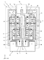
以下、本発明を適用可能な半導体モジュールについて説明する。図1は、本実施の形態に係る半導体装置の平面図である。図2は、図1に示す半導体装置をA−A線に沿って切断した断面図である。図3は、本実施の形態に係る回路板のレイアウトを示す平面図である。図4は、本実施の形態に係る半導体素子の平面図である。図5は、本実施の形態に係る出力端子の平面図である。図6は、本実施の形態に係るP端子及びN端子の平面図である。なお、以下に示す半導体モジュールはあくまで一例にすぎず、これに限定されることなく適宜変更が可能である。 Hereinafter, the semiconductor module to which the present invention can be applied will be described. FIG. 1 is a plan view of the semiconductor device according to the present embodiment. FIG. 2 is a cross-sectional view of the semiconductor device shown in FIG. 1 cut along the line AA. FIG. 3 is a plan view showing the layout of the circuit board according to the present embodiment. FIG. 4 is a plan view of the semiconductor element according to the present embodiment. FIG. 5 is a plan view of the output terminal according to the present embodiment. FIG. 6 is a plan view of the P terminal and the N terminal according to the present embodiment. The semiconductor modules shown below are merely examples, and the modules are not limited to these and can be changed as appropriate.
また、以下の図において、複数の半導体モジュールが並ぶ方向をX方向、直列接続される上アームと下アームの並び方向をY方向、高さ方向をZ方向と定義することにする。図示されたX、Y、Zの各軸は互いに直交し、右手系を成している。また、場合によっては、X方向を左右方向、Y方向を前後方向、Z方向を上下方向と呼ぶことがある。これらの方向(前後左右上下方向)は、説明の便宜上用いる文言であり、半導体装置の取付姿勢によっては、XYZ方向のそれぞれとの対応関係が変わることがある。例えば、半導体装置の放熱面側(冷却器側)を下面側とし、その反対側を上面側と呼ぶことにする。また、本明細書において、平面視は、半導体装置の上面をZ方向正側からみた場合を意味する。 Further, in the following figure, the direction in which a plurality of semiconductor modules are arranged is defined as the X direction, the arrangement direction of the upper arm and the lower arm connected in series is defined as the Y direction, and the height direction is defined as the Z direction. The illustrated X, Y, and Z axes are orthogonal to each other, forming a right-handed system. In some cases, the X direction may be referred to as a left-right direction, the Y direction may be referred to as a front-rear direction, and the Z direction may be referred to as a vertical direction. These directions (front-back, left-right, up-down directions) are terms used for convenience of explanation, and the correspondence with each of the XYZ directions may change depending on the mounting posture of the semiconductor device. For example, the heat dissipation surface side (cooler side) of the semiconductor device is referred to as the lower surface side, and the opposite side is referred to as the upper surface side. Further, in the present specification, the plan view means a case where the upper surface of the semiconductor device is viewed from the positive side in the Z direction.
本実施の形態に係る半導体装置は、例えばパワーモジュール等の電力変換装置に適用されるものであり、インバータ回路を構成するパワーモジュールである。半導体装置は、半導体モジュール1を備えている。図1では、単一の半導体モジュール1について説明する。例えば、半導体装置が三相インバータ回路を構成する場合、図1の半導体モジュールがU相、V相、W相の順にX方向に3つ並んで配置される。 The semiconductor device according to the present embodiment is applied to a power conversion device such as a power module, and is a power module constituting an inverter circuit. The semiconductor device includes a semiconductor module 1. FIG. 1 describes a single semiconductor module 1. For example, when a semiconductor device constitutes a three-phase inverter circuit, three semiconductor modules of FIG. 1 are arranged side by side in the X direction in the order of U phase, V phase, and W phase.
図1から図6に示すように、半導体モジュール1は、ベース板10と、ベース板10上に配置される積層基板2と、積層基板2上に配置される複数の半導体素子と、積層基板2及び半導体素子を収容するケース部材11と、ケース部材11内に充填される封止樹脂12と、を含んで構成される。
As shown in FIGS. 1 to 6, the semiconductor module 1 includes a
ベース板10は、上面と下面を有する長方形の板である。ベース板10は、放熱板として機能する。また、ベース板10は、X方向に長い平面視矩形状を有している。ベース板10は、例えば銅、アルミニウム又はこれらの合金等からなる金属板であり、表面にメッキ処理が施されてもよい。
The
ベース板10の上面には、平面視矩形状で且つ枠状のケース部材11が配置される。ケース部材11は、例えば合成樹脂によって成形され、接着剤(不図示)を介してベース板10の上面に接合される。ケース部材11の一側壁部13には、外部接続用の制御端子14が設けられている。例えば、ケース部材11のX方向で対向する一対の側壁部のうち、X方向正側の側壁部13に、制御端子14が一体成型により埋め込まれている。
A
制御端子14は、例えば銅素材、銅合金系素材、アルミニウム合金系素材、鉄合金系素材等の金属素材の板状体を折り曲げて形成される。制御端子14の一部は、側壁部13の上面に露出している。また、詳細は後述するが、ケース部材11のY方向で対向する一対の側壁部13において、Y方向正側には、ケース端子としての出力端子15(M端子)が設けられており、Y方向負側には、ケース端子としての正極端子16(P端子)及び負極端子17(N端子)が設けられている。
The
また、ケース部材11の内側において、ベース板10の上面には、積層基板2が配置されている。積層基板2は、金属層と絶縁層とを積層して形成され、例えば、DCB(Direct Copper Bonding)基板やAMB(Active Metal Brazing)基板、あるいは金属ベース基板で構成される。具体的に積層基板2は、絶縁板20と、絶縁板20の下面に配置された放熱板21と、絶縁板20の上面に配置された複数の回路板22と、を有する。積層基板2は、例えば平面視矩形状に形成される。
Further, inside the
絶縁板20は、Z方向に所定の厚みを有し、上面と下面を有する平板状に形成される。絶縁板20は、例えばアルミナ(Al2O3)、窒化アルミニウム(AlN)、窒化珪素(Si3N4)等のセラミックス材料、エポキシ等の樹脂材料、又はセラミックス材料をフィラーとして用いたエポキシ樹脂材料等の絶縁材料によって形成される。なお、絶縁板20は、絶縁層又は絶縁フィルムと呼ばれてもよい。
The insulating
放熱板21は、Z方向に所定の厚みを有し、絶縁板20の下面全体を覆うように形成される。放熱板21は、例えば銅やアルミニウム等の熱伝導性の良好な金属板によって形成される。
The
絶縁板20の上面(主面)には、複数の回路板22が、電気的に互いに絶縁された状態で、独立して島状に形成されている。複数の回路板22は、銅箔等によって形成される所定厚みの金属層で構成される。具体的に複数の回路板22は、Y方向(所定方向)に延在する第1〜第6導電層23−28を含んで構成される。第1〜第6導電層23−28は、X方向(Y方向に交差する方向)に並んで配置されている。具体的に複数の回路板22は、X方向負側から第1導電層23、第5導電層27、第3導電層25、第4導電層26、第6導電層28、第2導電層24、の順に配置されている。
On the upper surface (main surface) of the insulating
第1導電層23のY方向負側の端部は、第3導電層25のY方向負側の端部よりもY方向負側に位置している。第2導電層24のY方向負側の端部は、第4導電層26のY方向負側の端部よりもY方向負側に位置している。
The end of the first
第3導電層25及び第4導電層26は、第1導電層23と第2導電層24の間に挟まれるように配置されている。第5導電層27は、第1導電層23と第3導電層25の間に配置されている。第6導電層28は、第2導電層24と第4導電層26の間に配置されている。
The third
第5導電層27は、Y方向負側がクランク状に屈曲しており、その端部は、第1導電層23よりもX方向正側で且つ第3導電層25よりもY方向負側に位置している。第6導電層28は、Y方向負側がクランク状に屈曲しており、その端部は、第2導電層24よりもX方向負側で且つ第4導電層26よりもY方向負側に位置している。このように、第1導電層23、第3導電層25、及び第5導電層27と、第2導電層24、第4導電層26、及び第6導電層28とは、絶縁板20のX方向中央を挟んで鏡像配置されている。
The fifth
詳細は後述するが、第1導電層23及び第2導電層24のY方向負側の端部(他端側)は、正極端子16に接続される。また、第3導電層25及び第4導電層26のY方向正側の端部(一端側)は、出力端子15に接続される。更に、第5導電層27及び第6導電層28のY方向負側の端部(他端側)は、負極端子17に接続される。
Although details will be described later, the end portion (other end side) on the negative side in the Y direction of the first
また、第3導電層25と第4導電層26の間には、Y方向に延びて比較的幅の狭い制御用回路板29a−29cが配置されている。制御用回路板29a、29bは、Y方向正側においてX方向に並んで配置されており、制御用回路板29cは、Y方向負側に配置されている。これらの制御用回路板29a−29cには、制御用の配線(不図示)が接続される。
Further, between the third
回路板22の上面の所定箇所には、半田等の接合材(不図示)を介して複数の半導体素子3が配置されている。半導体素子は、例えばシリコン(Si)、炭化けい素(SiC)、窒化ガリウム(GaN)等の半導体基板によって平面視方形状に形成される。本実施の形態において、半導体素子は、IGBT(Insulated Gate Bipolar Transistor)素子とFWD(Free Wheeling Diode)素子の機能を一体化したRC(Reverse Conducting)−IGBT素子で構成される。
A plurality of semiconductor elements 3 are arranged at predetermined positions on the upper surface of the
なお、半導体素子は、これに限定されず、IGBT、パワーMOSFET(Metal Oxide Semiconductor Field Effect Transistor)、BJT(Bipolar Junction Transistor)等のスイッチング素子、FWD(Free Wheeling Diode)等のダイオードを組み合わせて構成されてもよい。また、半導体素子として、逆バイアスに対して十分な耐圧を有するRB(Reverse Blocking)−IGBT等を用いてもよい。また、半導体素子の形状、配置数、配置箇所等は適宜変更が可能である。 The semiconductor element is not limited to this, and is configured by combining a switching element such as an IGBT, a power MOSFET (Metal Oxide Semiconductor Field Effect Transistor), a BJT (Bipolar Junction Transistor), and a diode such as an FWD (Free Wheeling Diode). You may. Further, as the semiconductor element, an RB (Reverse Blocking) -IGBT or the like having a sufficient withstand voltage against reverse bias may be used. In addition, the shape, number of arrangements, arrangement locations, etc. of the semiconductor elements can be changed as appropriate.
本実施の形態では、1相につき、8つの半導体素子が配置されている。具体的に本実施の形態では、第1〜第4半導体素子3a−3dが、それぞれ2つずつ、Y方向に並んで配置されている。各半導体素子は、それぞれ上面電極(エミッタ電極又はソース電極と呼ばれてよい)と下面電極(コレクタ電極又はドレイン電極と呼ばれてよい)を有している。また、各半導体素子は、上面の外周側に偏ってゲート電極30(図4参照)が配置されている。2つずつ配置された各第1〜第4半導体素子3a−3dは、ゲート電極30がY方向で対向している。
In this embodiment, eight semiconductor elements are arranged for each phase. Specifically, in the present embodiment, two first to
第1半導体素子3aは、第1導電層23の上面に配置されている。すなわち、第1半導体素子3aの下面電極は、第1導電層23に導電接続されている。2つの第1半導体素子3aは、第1導電層23のY方向正側に偏って配置され、並列接続されている。
The
第2半導体素子3bは、第2導電層24の上面に配置されている。すなわち、第2半導体素子3bの下面電極は、第2導電層24に導電接続されている。2つの第2半導体素子3bは、第2導電層24のY方向正側に偏って配置され、並列接続されている。
The
第3半導体素子3cは、第3導電層25の上面に配置されている。すなわち、第3半導体素子3cの下面電極は、第3導電層25に導電接続されている。2つの第3半導体素子3cは、第3導電層25のY方向負側に偏って配置され、並列接続されている。
The
第4半導体素子3dは、第4導電層26の上面に配置されている。すなわち、第4半導体素子3dの下面電極は、第4導電層26に導電接続されている。2つの第4半導体素子3dは、第4導電層26のY方向負側に偏って配置され、並列接続されている。
The fourth semiconductor element 3d is arranged on the upper surface of the fourth
第1半導体素子3a及び第2半導体素子3bは、上アームを構成し、第3半導体素子3c及び第4半導体素子3dは、下アームを構成する。上アームと下アームは、直列接続される。図1に示すように、第1半導体素子3a及び第2半導体素子3bは、後述する出力端子15側に偏って配置されており、第3半導体素子3c及び第4半導体素子3dは、負極端子17側に偏って配置されている。
The
また、第1半導体素子3a及び第3半導体素子3cと、第2半導体素子3b及び第4半導体素子3dとは、積層基板2のX方向中央を挟んで鏡像配置されている。また、上アームを構成する第1半導体素子3a及び第2半導体素子3bは、積層基板2のX方向中央から遠ざけて配置されているのに対し、下アームを構成する第3半導体素子3c及び第4半導体素子3dは、積層基板2のX方向中央に近づけて配置されている。
Further, the
また、各半導体素子の上面電極と所定の回路板22とは、主電流配線部材としての金属配線板(第1〜第4配線4a−4d)により電気的に接続される。第1配線4aは、第1半導体素子3aの上面電極と第3導電層25を接続する。第2配線4bは、第2半導体素子3bの上面電極と第4導電層26を接続する。第3配線4cは、第3半導体素子3cの上面電極と第5導電層27を接続する。第4配線4dは、第4半導体素子3dの上面電極と第6導電層28を接続する。
Further, the top electrode of each semiconductor element and the
金属配線板は、例えば、銅素材、銅合金系素材、アルミニウム合金系素材、鉄合金系素材等の金属素材を用いて、プレス加工等によって折り曲げて形成される。なお、各金属配線板は、全て同じ構成を有するため、共通の符号を付して説明する。具体的に金属配線板は、図4に示すように、所定の半導体素子の上面電極に接合される第1接合部40と、所定の回路板22に接合される第2接合部41と、第1接合部40及び第2接合部41を連結する連結部42と、によって構成される。なお、図4に示す金属配線板の形状はあくまで一例を示すものであり、適宜変更が可能である。また、金属配線板は、リードフレームと呼ばれてもよい。また、各金属配線板(第1〜第4配線4a−4d)は、図1に示す平面視において、X方向に延びている。
The metal wiring plate is formed by bending a metal material such as a copper material, a copper alloy material, an aluminum alloy material, or an iron alloy material by press working or the like. Since all the metal wiring boards have the same configuration, they will be described with a common reference numeral. Specifically, as shown in FIG. 4, the metal wiring board has a first joining
また、ケース部材11には、上記したように主電流の外部接続用のケース端子として、出力端子15、正極端子16、及び負極端子17が設けられている。出力端子15は、ケース部材11のY方向で対向する一対の側壁部13のY方向正側に配置されている。正極端子16及び負極端子17は、ケース部材11のY方向で対向する一対の側壁部13のY方向負側に配置されている。
Further, as described above, the
これらのケース端子は、例えば、銅素材、銅合金系素材、アルミニウム合金系素材、鉄合金系素材等の金属素材を用いて、プレス加工等によって形成される。図1及び図5に示すように、出力端子15は、2つに分岐した出力端部15a、15bを有している。出力端部15a、15bは、X方向に並んで配置されている。X方向負側に位置する出力端部15aは、第3導電層25のY方向正側の端部(一端側)に接続されている。X方向正側に位置する出力端部15bは、第4導電層26のY方向正側の端部(一端側)に接続されている。詳細は後述するが、第3導電層25及び第4導電層26は、出力端子15に接続されることで、同電位となっている。
These case terminals are formed by press working or the like using, for example, a metal material such as a copper material, a copper alloy material, an aluminum alloy material, or an iron alloy material. As shown in FIGS. 1 and 5, the
図1及び図6に示すように、正極端子16は、2つに分岐した正極端部16a、16bを有している。正極端部16a、16bは、所定間隔を空けてX方向に並んで配置されている。正極端部16a、16bは、間に負極端子17を挟んでいる。X方向負側に位置する正極端部16aは、第1導電層23のY方向負側の端部(他端側)に接続されている。X方向正側に位置する正極端部16bは、第2導電層24のY方向負側の端部(他端側)に接続されている。
As shown in FIGS. 1 and 6, the
図1及び図6に示すように、負極端子17は、2つに分岐した負極端部17a、17bを有している。負極端部17a、17bは、正極端部16a、16bの間に挟まれるように、X方向に並んで配置されている。X方向負側に位置する負極端部17aは、第5導電層27のY方向負側の端部(他端側)に接続されている。X方向正側に位置する負極端部17bは、第6導電層28のY方向負側の端部(他端側)に接続されている。
As shown in FIGS. 1 and 6, the
ところで、半導体モジュールにおいては、PN端子間のインダクタンスがスイッチング損失に影響を及ぼすことから、そのインダクタンスの低減が求められている。また、昨今の技術革新に伴って、SiCやGaN等の次世代デバイス(ワイドバンドギャップ半導体と呼ばれてもよい)が採用されると、スイッチングの周波数が高周波化(例えば20〜100kHz)することが予想される。この場合、電流の表皮効果により絶縁基板の回路板端部に電流が集中することで当該端部が異常発熱してしまうという問題がある。これは、従来の比較的低い周波数(10kHz以下)では、問題とはならなかった。なお、表皮効果とは、導電層の端部に電流が偏って流れる現象をいう。 By the way, in a semiconductor module, since the inductance between PN terminals affects the switching loss, it is required to reduce the inductance. In addition, with the recent technological innovation, when next-generation devices such as SiC and GaN (which may be called wide bandgap semiconductors) are adopted, the switching frequency becomes higher (for example, 20 to 100 kHz). Is expected. In this case, there is a problem that the current concentrates on the end portion of the circuit board of the insulating substrate due to the skin effect of the current, and the end portion abnormally generates heat. This was not a problem at conventional relatively low frequencies (10 kHz or less). The skin effect is a phenomenon in which an electric current flows unevenly at the end of the conductive layer.
そこで、本件発明者等は、絶縁基板の回路板、半導体素子、及びケース端子のレイアウトに着目し、本発明に想到した。図7は、本実施の形態に係る半導体モジュールの電流の流れを示す模式図である。具体的に本実施の形態では、図7に示すように、半導体素子が配置される複数の回路板を所定方向に延ばして形成し、当該所定方向に交差する方向で複数の回路板を並べる構成とした。また、複数の回路板のうち、内側に位置する所定の回路板(第3導電層25及び第4導電層26)は、ケース端子としての出力端子15に接続されることで同電位となっている。
Therefore, the present inventors have focused on the layout of the circuit board of the insulating substrate, the semiconductor element, and the case terminal, and came up with the present invention. FIG. 7 is a schematic view showing a current flow of the semiconductor module according to the present embodiment. Specifically, in the present embodiment, as shown in FIG. 7, a plurality of circuit boards on which semiconductor elements are arranged are formed by extending them in a predetermined direction, and a plurality of circuit boards are arranged in a direction intersecting the predetermined directions. And said. Further, among the plurality of circuit boards, the predetermined circuit boards (third
より具体的には、出力端子15は、Y方向正側の端部に設けられ、2つに分岐した出力端部15a、15bを有している。また、一方の出力端部15aは、第3導電層25の一端側に接続され、他方の出力端部15bは、第4導電層26の一端側に接続されている。
More specifically, the
また、Y方向負側の端部には、2つに分岐した正極端部16a、16bを有する正極端子16が設けられている。一方の正極端部16aは、第1導電層23の他端側に接続され、他方の正極端部16bは、第2導電層24の他端側に接続されている。すなわち、第1半導体素子3a及び第2半導体素子3bは、上アームを構成する。
Further, a
また、Y方向負側の端部には、2つに分岐した負極端部17a、17bを有する負極端子17が設けられている。更に、第1導電層23と第3導電層25の間に第5導電層が配置され、第2導電層24と第4導電層26の間に第6導電層28が配置されている。一方の負極端部17aは、第5導電層27の他端側に接続され、他方の負極端部17bは、第6導電層28の他端側に接続されている。すなわち、第3半導体素子3c及び第4半導体素子3dは、下アームを構成する。
Further, a
このように、本実施の形態では、PN間のインダクタンスを下げるために、
(1)主電流の流れる並列数を従来の1列から2列に増やした。
(2)P端子とN端子間の電流経路ができる限り近くなるように互いに平行となるような配線パターン(回路板のレイアウト)とした。
As described above, in the present embodiment, in order to reduce the inductance between PNs,
(1) The number of parallel lines in which the main current flows has been increased from the conventional one row to two rows.
(2) The wiring pattern (circuit board layout) is set so that the current paths between the P terminal and the N terminal are parallel to each other so as to be as close as possible.
図7に示すように、半導体モジュール1では、正極端子16から流れる主電流が両外側の正極端部16a、16bにより2つに分流される。主電流は、第1導電層23(第2導電層24)から上アームの第1半導体素子3a(第2半導体素子3b)を経由して第3導電層25(第4導電層26)を流れる。更に主電流は、下アームの第3半導体素子3c(第4半導体素子3d)を経由して第5導電層27(第6導電層28)から負極端部17a(負極端部17b)に流れ込む。
As shown in FIG. 7, in the semiconductor module 1, the main current flowing from the
このように、本実施の形態では、電流経路となる回路板のレイアウトを複数の直線で構成したことにより、電流経路が複数に分散される。この結果、1つの回路板において表皮効果によって端部に流れる電流が分散され、回路板の端部において、過度の発熱を防止することが可能なっている。また、図7に示すように、上アームの電流経路F1と下アームの電流経路F2が平行で隣接しており、互いに逆方向に主電流が流れている。よって、相互インダクタンスの効果により、低インダクタンス化を実現でき、スイッチング損失が低減される。また、各ケース端子の端部を複数に分岐する構成としたことで、樹脂で封止したときの他の部材同士間における密着度が向上され、剥がれ難くすることが可能である。また、上記したように全体のレイアウトが鏡像配置となっているため、電流経路を2つに分けても電流の偏りが生じ難くなり、局所的な発熱を抑制することが可能になっている。 As described above, in the present embodiment, the current path is dispersed into a plurality of lines by configuring the layout of the circuit board serving as the current path with a plurality of straight lines. As a result, the current flowing to the end portion of one circuit board is dispersed by the skin effect, and it is possible to prevent excessive heat generation at the end portion of the circuit board. Further, as shown in FIG. 7, the current path F1 of the upper arm and the current path F2 of the lower arm are parallel and adjacent to each other, and the main currents flow in opposite directions. Therefore, due to the effect of mutual inductance, low inductance can be realized and switching loss is reduced. Further, by adopting a configuration in which the end portion of each case terminal is branched into a plurality of parts, the degree of adhesion between other members when sealed with a resin is improved, and it is possible to prevent the case terminals from peeling off. Further, since the entire layout is a mirror image arrangement as described above, even if the current path is divided into two, the current is less likely to be biased, and it is possible to suppress local heat generation.
以上説明したように、本実施の形態によれば、PN端子間のインダクタンスを低減することが可能である。 As described above, according to the present embodiment, it is possible to reduce the inductance between the PN terminals.
また、上記実施の形態において、半導体素子の個数及び配置箇所は、上記構成に限定されず、適宜変更が可能である。 Further, in the above embodiment, the number and arrangement locations of the semiconductor elements are not limited to the above configuration, and can be appropriately changed.
また、上記実施の形態において、回路板の個数及びレイアウトは、上記構成に限定されず、適宜変更が可能である。 Further, in the above embodiment, the number and layout of the circuit boards are not limited to the above configuration and can be changed as appropriate.
また、上記実施の形態では、積層基板2や半導体素子が平面視矩形状又は方形状に形成される構成としたが、この構成に限定されない。積層基板2や半導体素子は、上記以外の多角形状に形成されてもよい。
Further, in the above embodiment, the
また、本実施の形態及び変形例を説明したが、他の実施の形態として、上記実施の形態及び変形例を全体的又は部分的に組み合わせたものでもよい。 Moreover, although the present embodiment and the modified example have been described, as another embodiment, the above-described embodiment and the modified example may be combined in whole or in part.
また、本実施の形態は上記の実施の形態及び変形例に限定されるものではなく、技術的思想の趣旨を逸脱しない範囲において様々に変更、置換、変形されてもよい。さらに、技術の進歩又は派生する別技術によって、技術的思想を別の仕方で実現することができれば、その方法を用いて実施されてもよい。したがって、特許請求の範囲は、技術的思想の範囲内に含まれ得る全ての実施態様をカバーしている。 Further, the present embodiment is not limited to the above-described embodiment and modification, and may be variously modified, replaced, or modified without departing from the spirit of the technical idea. Further, if the technical idea can be realized in another way by the advancement of the technology or another technology derived from it, it may be carried out by using that method. Therefore, the claims cover all embodiments that may be included within the scope of the technical idea.
下記に、上記実施の形態における特徴点を整理する。
上記実施の形態に記載の半導体モジュールは、それぞれ上面電極と下面電極を有する第1半導体素子、第2半導体素子、第3半導体素子、及び第4半導体素子と、所定方向に延在し、それぞれ独立して前記所定方向に交差する方向に並んで配置された第1導電層、第2導電層、第3導電層、及び第4導電層と、前記第2導電層及び前記第3導電層に接続されたケース端子と、を備え、前記第1半導体素子の下面電極は、前記第1導電層に導電接続され、前記第2半導体素子の下面電極は、前記第2導電層に導電接続され、前記第3半導体素子の下面電極は、前記第3導電層に導電接続され、前記第4半導体素子の下面電極は、前記第4導電層に導電接続され、前記第3導電層及び前記第4導電層は、前記第1導電層と前記第2導電層の間に挟まれるように配置され、前記ケース端子に接続されて同電位である。
The feature points in the above embodiment are summarized below.
The semiconductor module according to the above embodiment extends in a predetermined direction from a first semiconductor element, a second semiconductor element, a third semiconductor element, and a fourth semiconductor element having an upper surface electrode and a lower surface electrode, respectively, and is independent of each other. Then, the first conductive layer, the second conductive layer, the third conductive layer, and the fourth conductive layer arranged side by side in the direction intersecting the predetermined directions are connected to the second conductive layer and the third conductive layer. The lower surface electrode of the first semiconductor element is conductively connected to the first conductive layer, and the lower surface electrode of the second semiconductor element is conductively connected to the second conductive layer. The lower surface electrode of the third semiconductor element is conductively connected to the third conductive layer, the lower surface electrode of the fourth semiconductor element is conductively connected to the fourth conductive layer, and the third conductive layer and the fourth conductive layer are conductively connected. Is arranged so as to be sandwiched between the first conductive layer and the second conductive layer, and is connected to the case terminal and has the same potential.
また、上記の半導体モジュールにおいて、前記ケース端子は、少なくとも2つに分岐した出力端部を有する出力端子で構成され、一方の前記出力端部は、前記第3導電層の一端側に接続され、他方の前記出力端部は、前記第4導電層の一端側に接続されている。 Further, in the above semiconductor module, the case terminal is composed of an output terminal having at least two branched output ends, and one of the output ends is connected to one end side of the third conductive layer. The other output end is connected to one end side of the fourth conductive layer.
また、上記の半導体モジュールは、少なくとも2つに分岐した正極端部を有する正極端子を更に備え、前記第1半導体素子及び前記第2半導体素子は、上アームを構成し、一方の前記正極端部は、前記第1導電層の他端側に接続され、他方の前記正極端部は、前記第2導電層の他端側に接続されている。 Further, the semiconductor module further includes a positive electrode terminal having a positive electrode end portion branched into at least two, and the first semiconductor element and the second semiconductor element form an upper arm, and one of the positive electrode end portions. Is connected to the other end side of the first conductive layer, and the other positive electrode end is connected to the other end side of the second conductive layer.
また、上記の半導体モジュールは、少なくとも2つに分岐した負極端部を有する負極端子と、前記所定方向に延び、前記第1導電層と前記第3導電層の間に配置された第5導電層と、前記所定方向に延び、前記第2導電層と前記第4導電層の間に配置された第6導電層と、を更に備え、前記第3半導体素子及び前記第4半導体素子は、下アームを構成し、一方の前記負極端部は、前記第5導電層の他端側に接続され、他方の前記負極端部は、前記第6導電層の他端側に接続され、一方及び他方の前記負極端部は、一方及び他方の前記正極端部の間に挟まれるように配置されている。 Further, the semiconductor module has a negative electrode terminal having at least two branched negative electrode ends, and a fifth conductive layer extending in a predetermined direction and arranged between the first conductive layer and the third conductive layer. And a sixth conductive layer extending in the predetermined direction and arranged between the second conductive layer and the fourth conductive layer, and the third semiconductor element and the fourth semiconductor element are lower arms. One of the negative electrode ends is connected to the other end of the fifth conductive layer, and the other negative end is connected to the other end of the sixth conductive layer. The negative electrode end is arranged so as to be sandwiched between one and the other positive end.
また、上記の半導体モジュールにおいて、前記第1半導体素子及び前記第2半導体素子は、前記出力端子側に偏って配置され、前記第3半導体素子及び前記第4半導体素子は、前記負極端子側に偏って配置されている。 Further, in the above semiconductor module, the first semiconductor element and the second semiconductor element are biased toward the output terminal side, and the third semiconductor element and the fourth semiconductor element are biased toward the negative electrode terminal side. Is arranged.
また、上記の半導体モジュールは、前記第1半導体素子の上面電極と前記第3導電層を接続する第1配線と、前記第2半導体素子の上面電極と前記第4導電層を接続する第2配線と、前記第3半導体素子の上面電極と前記第5導電層を接続する第3配線と、前記第4半導体素子の上面電極と前記第6導電層を接続する第4配線と、を更に備え、前記第1配線、前記第2配線、前記第3配線、及び前記第4配線は、前記所定方向に交差する方向に延びている。 Further, the semiconductor module includes a first wiring that connects the upper surface electrode of the first semiconductor element and the third conductive layer, and a second wiring that connects the upper surface electrode of the second semiconductor element and the fourth conductive layer. A third wiring for connecting the upper surface electrode of the third semiconductor element and the fifth conductive layer, and a fourth wiring for connecting the upper surface electrode of the fourth semiconductor element and the sixth conductive layer are further provided. The first wiring, the second wiring, the third wiring, and the fourth wiring extend in a direction intersecting the predetermined direction.
また、上記の半導体モジュールにおいて、前記第1半導体素子、前記第2半導体素子、前記第3半導体素子、及び前記第4半導体素子は、それぞれ複数ずつ、前記所定方向に並んで配置されている。 Further, in the above-mentioned semiconductor module, a plurality of the first semiconductor element, the second semiconductor element, the third semiconductor element, and the fourth semiconductor element are arranged side by side in the predetermined direction.
また、上記の半導体モジュールにおいて、前記第1半導体素子、前記第3半導体素子、前記第1導電層、前記第3導電層、及び前記第5導電層と、前記第2半導体素子、前記第4半導体素子、前記第2導電層、前記第4導電層、及び前記第6導電層とは、鏡像配置されている。 Further, in the above semiconductor module, the first semiconductor element, the third semiconductor element, the first conductive layer, the third conductive layer, the fifth conductive layer, the second semiconductor element, and the fourth semiconductor. The element, the second conductive layer, the fourth conductive layer, and the sixth conductive layer are arranged in a mirror image.
以上説明したように、本発明は、PN端子間のインダクタンスを低減すると共に、端子の発熱を分散させることができるという効果を有し、特に、半導体モジュールに有用である。 As described above, the present invention has the effect of reducing the inductance between the PN terminals and dispersing the heat generated by the terminals, and is particularly useful for semiconductor modules.
1 :半導体モジュール
2 :積層基板
3a :第1半導体素子
3b :第2半導体素子
3c :第3半導体素子
3d :第4半導体素子
4a :第1配線
4b :第2配線
4c :第3配線
4d :第4配線
10 :ベース板
11 :ケース部材
12 :封止樹脂
13 :側壁部
14 :制御端子
15 :出力端子
15a :出力端部
15b :出力端部
16 :正極端子
16a :正極端部
16b :正極端部
17 :負極端子
17a :負極端部
17b :負極端部
20 :絶縁板
21 :放熱板
22 :回路板
23 :第1導電層
24 :第2導電層
25 :第3導電層
26 :第4導電層
27 :第5導電層
28 :第6導電層
29a :制御用回路板
29b :制御用回路板
29c :制御用回路板
30 :ゲート電極
40 :第1接合部
41 :第2接合部
42 :連結部
F1 :電流経路
F2 :電流経路
1: Semiconductor module 2: Laminated
Claims (8)
所定方向に延在し、それぞれ独立して前記所定方向に交差する方向に並んで配置された第1導電層、第2導電層、第3導電層、及び第4導電層と、
前記第2導電層及び前記第3導電層に接続されたケース端子と、を備え、
前記第1半導体素子の下面電極は、前記第1導電層に導電接続され、
前記第2半導体素子の下面電極は、前記第2導電層に導電接続され、
前記第3半導体素子の下面電極は、前記第3導電層に導電接続され、
前記第4半導体素子の下面電極は、前記第4導電層に導電接続され、
前記第3導電層及び前記第4導電層は、前記第1導電層と前記第2導電層の間に挟まれるように配置され、前記ケース端子に接続されて同電位である、半導体モジュール。 A first semiconductor element, a second semiconductor element, a third semiconductor element, and a fourth semiconductor element having an upper surface electrode and a lower surface electrode, respectively.
The first conductive layer, the second conductive layer, the third conductive layer, and the fourth conductive layer, which extend in a predetermined direction and are independently arranged side by side in a direction intersecting the predetermined direction,
The second conductive layer and the case terminal connected to the third conductive layer are provided.
The bottom electrode of the first semiconductor element is conductively connected to the first conductive layer.
The bottom electrode of the second semiconductor element is conductively connected to the second conductive layer.
The bottom electrode of the third semiconductor element is conductively connected to the third conductive layer.
The bottom electrode of the fourth semiconductor element is conductively connected to the fourth conductive layer.
A semiconductor module in which the third conductive layer and the fourth conductive layer are arranged so as to be sandwiched between the first conductive layer and the second conductive layer, and are connected to the case terminals to have the same potential.
一方の前記出力端部は、前記第3導電層の一端側に接続され、
他方の前記出力端部は、前記第4導電層の一端側に接続されている、請求項1に記載の半導体モジュール。 The case terminal is composed of an output terminal having an output end branched into at least two.
One of the output ends is connected to one end side of the third conductive layer.
The semiconductor module according to claim 1, wherein the other output end is connected to one end side of the fourth conductive layer.
前記第1半導体素子及び前記第2半導体素子は、上アームを構成し、
一方の前記正極端部は、前記第1導電層の他端側に接続され、
他方の前記正極端部は、前記第2導電層の他端側に接続されている、請求項2に記載の半導体モジュール。 Further provided with a positive electrode terminal having a positive electrode end branched into at least two,
The first semiconductor element and the second semiconductor element constitute an upper arm, and the first semiconductor element and the second semiconductor element form an upper arm.
One end of the positive electrode is connected to the other end of the first conductive layer.
The semiconductor module according to claim 2, wherein the other positive end is connected to the other end of the second conductive layer.
前記所定方向に延び、前記第1導電層と前記第3導電層の間に配置された第5導電層と、
前記所定方向に延び、前記第2導電層と前記第4導電層の間に配置された第6導電層と、を更に備え、
前記第3半導体素子及び前記第4半導体素子は、下アームを構成し、
一方の前記負極端部は、前記第5導電層の他端側に接続され、
他方の前記負極端部は、前記第6導電層の他端側に接続され、
一方及び他方の前記負極端部は、一方及び他方の前記正極端部の間に挟まれるように配置されている、請求項3に記載の半導体モジュール。 A negative electrode terminal having a negative electrode end branched into at least two, and a negative electrode terminal.
A fifth conductive layer extending in a predetermined direction and arranged between the first conductive layer and the third conductive layer,
A sixth conductive layer extending in the predetermined direction and arranged between the second conductive layer and the fourth conductive layer is further provided.
The third semiconductor element and the fourth semiconductor element constitute a lower arm, and the third semiconductor element and the fourth semiconductor element form a lower arm.
One end of the negative electrode is connected to the other end of the fifth conductive layer.
The other end of the negative electrode is connected to the other end of the sixth conductive layer.
The semiconductor module according to claim 3, wherein the negative electrode ends of one and the other are arranged so as to be sandwiched between the positive electrode ends of one and the other.
前記第3半導体素子及び前記第4半導体素子は、前記負極端子側に偏って配置されている、請求項4に記載の半導体モジュール。 The first semiconductor element and the second semiconductor element are arranged unevenly on the output terminal side.
The semiconductor module according to claim 4, wherein the third semiconductor element and the fourth semiconductor element are unevenly arranged on the negative electrode terminal side.
前記第2半導体素子の上面電極と前記第4導電層を接続する第2配線と、
前記第3半導体素子の上面電極と前記第5導電層を接続する第3配線と、
前記第4半導体素子の上面電極と前記第6導電層を接続する第4配線と、を更に備え、
前記第1配線、前記第2配線、前記第3配線、及び前記第4配線は、前記所定方向に交差する方向に延びている、請求項4又は請求項5に記載の半導体モジュール。 The first wiring connecting the upper surface electrode of the first semiconductor element and the third conductive layer, and
A second wiring connecting the upper surface electrode of the second semiconductor element and the fourth conductive layer, and
A third wiring connecting the upper surface electrode of the third semiconductor element and the fifth conductive layer, and
A fourth wiring for connecting the upper surface electrode of the fourth semiconductor element and the sixth conductive layer is further provided.
The semiconductor module according to claim 4 or 5, wherein the first wiring, the second wiring, the third wiring, and the fourth wiring extend in a direction intersecting the predetermined direction.
Priority Applications (2)
| Application Number | Priority Date | Filing Date | Title |
|---|---|---|---|
| JP2020038369A JP7532813B2 (en) | 2020-03-06 | 2020-03-06 | Semiconductor Module |
| US17/187,668 US11398448B2 (en) | 2020-03-06 | 2021-02-26 | Semiconductor module |
Applications Claiming Priority (1)
| Application Number | Priority Date | Filing Date | Title |
|---|---|---|---|
| JP2020038369A JP7532813B2 (en) | 2020-03-06 | 2020-03-06 | Semiconductor Module |
Publications (2)
| Publication Number | Publication Date |
|---|---|
| JP2021141222A true JP2021141222A (en) | 2021-09-16 |
| JP7532813B2 JP7532813B2 (en) | 2024-08-14 |
Family
ID=77556517
Family Applications (1)
| Application Number | Title | Priority Date | Filing Date |
|---|---|---|---|
| JP2020038369A Active JP7532813B2 (en) | 2020-03-06 | 2020-03-06 | Semiconductor Module |
Country Status (2)
| Country | Link |
|---|---|
| US (1) | US11398448B2 (en) |
| JP (1) | JP7532813B2 (en) |
Cited By (3)
| Publication number | Priority date | Publication date | Assignee | Title |
|---|---|---|---|---|
| WO2023189266A1 (en) * | 2022-03-28 | 2023-10-05 | 富士電機株式会社 | Metal wiring board |
| WO2023189265A1 (en) * | 2022-03-28 | 2023-10-05 | 富士電機株式会社 | Semiconductor module |
| DE112023000179T5 (en) | 2022-04-13 | 2024-04-25 | Fuji Electric Co., Ltd. | semiconductor device |
Families Citing this family (3)
| Publication number | Priority date | Publication date | Assignee | Title |
|---|---|---|---|---|
| CN114765434A (en) * | 2022-04-21 | 2022-07-19 | 苏州汇川联合动力系统有限公司 | Power module and motor controller |
| DE102022205510A1 (en) * | 2022-05-31 | 2023-11-30 | Vitesco Technologies GmbH | Power module, inverter with a power module |
| FR3147461A1 (en) * | 2023-03-31 | 2024-10-04 | Valeo Eautomotive Germany Gmbh | POWER MODULE |
Citations (2)
| Publication number | Priority date | Publication date | Assignee | Title |
|---|---|---|---|---|
| JPH07297362A (en) * | 1992-08-26 | 1995-11-10 | Eupec Europ G Fur Leistungshalbleiter Mbh & Co Kg | Power semiconductor module |
| WO2015104914A1 (en) * | 2014-01-09 | 2015-07-16 | 日立オートモティブシステムズ株式会社 | Semiconductor device and power conversion device using same |
Family Cites Families (9)
| Publication number | Priority date | Publication date | Assignee | Title |
|---|---|---|---|---|
| JP4496896B2 (en) | 2004-09-02 | 2010-07-07 | トヨタ自動車株式会社 | Power converter |
| JP4988676B2 (en) | 2008-09-16 | 2012-08-01 | 三菱電機株式会社 | Semiconductor circuit device |
| CN102460695A (en) | 2009-06-19 | 2012-05-16 | 株式会社安川电机 | Wiring board and power conversion device |
| US8637964B2 (en) | 2011-10-26 | 2014-01-28 | Infineon Technologies Ag | Low stray inductance power module |
| CN111048491B (en) | 2012-03-01 | 2023-04-18 | 三菱电机株式会社 | Power semiconductor module and power conversion device |
| JP6123500B2 (en) | 2013-06-05 | 2017-05-10 | 住友電気工業株式会社 | Semiconductor module |
| DE102014116662B4 (en) | 2014-11-14 | 2018-03-08 | Infineon Technologies Ag | ELECTRICAL CONNECTION ASSEMBLY, SEMICONDUCTOR MODULE AND METHOD FOR PRODUCING A SEMICONDUCTOR MODULE |
| EP3480846B1 (en) | 2017-11-03 | 2025-02-19 | Infineon Technologies AG | Semiconductor arrangement with reliably switching controllable semiconductor elements |
| JP7119666B2 (en) | 2018-07-09 | 2022-08-17 | 株式会社アイシン | Switching element unit and switching element module |
-
2020
- 2020-03-06 JP JP2020038369A patent/JP7532813B2/en active Active
-
2021
- 2021-02-26 US US17/187,668 patent/US11398448B2/en active Active
Patent Citations (2)
| Publication number | Priority date | Publication date | Assignee | Title |
|---|---|---|---|---|
| JPH07297362A (en) * | 1992-08-26 | 1995-11-10 | Eupec Europ G Fur Leistungshalbleiter Mbh & Co Kg | Power semiconductor module |
| WO2015104914A1 (en) * | 2014-01-09 | 2015-07-16 | 日立オートモティブシステムズ株式会社 | Semiconductor device and power conversion device using same |
Cited By (3)
| Publication number | Priority date | Publication date | Assignee | Title |
|---|---|---|---|---|
| WO2023189266A1 (en) * | 2022-03-28 | 2023-10-05 | 富士電機株式会社 | Metal wiring board |
| WO2023189265A1 (en) * | 2022-03-28 | 2023-10-05 | 富士電機株式会社 | Semiconductor module |
| DE112023000179T5 (en) | 2022-04-13 | 2024-04-25 | Fuji Electric Co., Ltd. | semiconductor device |
Also Published As
| Publication number | Publication date |
|---|---|
| US11398448B2 (en) | 2022-07-26 |
| JP7532813B2 (en) | 2024-08-14 |
| US20210280550A1 (en) | 2021-09-09 |
Similar Documents
| Publication | Publication Date | Title |
|---|---|---|
| JP7532813B2 (en) | Semiconductor Module | |
| JP5121133B2 (en) | Power module assembly and three-phase inverter assembly | |
| JP7428018B2 (en) | semiconductor module | |
| JP7428017B2 (en) | semiconductor module | |
| US8421087B2 (en) | Semiconductor module including a switch and non-central diode | |
| JP2002026251A (en) | Semiconductor device | |
| JP2000164800A (en) | Semiconductor module | |
| US7148562B2 (en) | Power semiconductor device and power semiconductor module | |
| CN113557603B (en) | Semiconductor device with a semiconductor device having a plurality of semiconductor chips | |
| CN113823625A (en) | Power Modules and Motor Controllers | |
| JP7491043B2 (en) | Semiconductor Module | |
| CN112582356A (en) | Semiconductor device with a plurality of transistors | |
| US11335660B2 (en) | Semiconductor module | |
| JPWO2021002132A1 (en) | Circuit structure of semiconductor module | |
| JP2021158232A (en) | Semiconductor module | |
| JP7142784B2 (en) | electric circuit device | |
| WO2022059251A1 (en) | Semiconductor device | |
| US20230335460A1 (en) | Semiconductor module | |
| JP7231109B2 (en) | Electric circuits and semiconductor modules | |
| JP7118204B1 (en) | semiconductor equipment | |
| US11887905B2 (en) | Semiconductor device | |
| WO2022075003A1 (en) | Semiconductor device | |
| US20240355713A1 (en) | Semiconductor device | |
| CN216120276U (en) | Double-side heat dissipation power MOSFET semiconductor device | |
| JPH10163416A (en) | Power semiconductor module |
Legal Events
| Date | Code | Title | Description |
|---|---|---|---|
| A621 | Written request for application examination |
Free format text: JAPANESE INTERMEDIATE CODE: A621 Effective date: 20230213 |
|
| RD03 | Notification of appointment of power of attorney |
Free format text: JAPANESE INTERMEDIATE CODE: A7423 Effective date: 20231019 |
|
| A977 | Report on retrieval |
Free format text: JAPANESE INTERMEDIATE CODE: A971007 Effective date: 20231031 |
|
| A131 | Notification of reasons for refusal |
Free format text: JAPANESE INTERMEDIATE CODE: A131 Effective date: 20231128 |
|
| A601 | Written request for extension of time |
Free format text: JAPANESE INTERMEDIATE CODE: A601 Effective date: 20240126 |
|
| A521 | Request for written amendment filed |
Free format text: JAPANESE INTERMEDIATE CODE: A523 Effective date: 20240326 |
|
| TRDD | Decision of grant or rejection written | ||
| A01 | Written decision to grant a patent or to grant a registration (utility model) |
Free format text: JAPANESE INTERMEDIATE CODE: A01 Effective date: 20240702 |
|
| A61 | First payment of annual fees (during grant procedure) |
Free format text: JAPANESE INTERMEDIATE CODE: A61 Effective date: 20240715 |
|
| R150 | Certificate of patent or registration of utility model |
Ref document number: 7532813 Country of ref document: JP Free format text: JAPANESE INTERMEDIATE CODE: R150 |