JP2021093609A - Surface acoustic wave filter, duplexer, and module - Google Patents
Surface acoustic wave filter, duplexer, and module Download PDFInfo
- Publication number
- JP2021093609A JP2021093609A JP2019222544A JP2019222544A JP2021093609A JP 2021093609 A JP2021093609 A JP 2021093609A JP 2019222544 A JP2019222544 A JP 2019222544A JP 2019222544 A JP2019222544 A JP 2019222544A JP 2021093609 A JP2021093609 A JP 2021093609A
- Authority
- JP
- Japan
- Prior art keywords
- piezoelectric layer
- resonator
- wave filter
- thickness
- resonators
- Prior art date
- Legal status (The legal status is an assumption and is not a legal conclusion. Google has not performed a legal analysis and makes no representation as to the accuracy of the status listed.)
- Granted
Links
- 238000010897 surface acoustic wave method Methods 0.000 title claims abstract description 25
- 239000000758 substrate Substances 0.000 claims abstract description 32
- 239000000463 material Substances 0.000 claims abstract description 10
- 239000012212 insulator Substances 0.000 claims abstract description 4
- 239000004065 semiconductor Substances 0.000 claims abstract description 4
- 230000008878 coupling Effects 0.000 claims description 6
- 238000010168 coupling process Methods 0.000 claims description 6
- 238000005859 coupling reaction Methods 0.000 claims description 6
- 238000010586 diagram Methods 0.000 description 23
- VYPSYNLAJGMNEJ-UHFFFAOYSA-N Silicium dioxide Chemical compound O=[Si]=O VYPSYNLAJGMNEJ-UHFFFAOYSA-N 0.000 description 14
- 230000000694 effects Effects 0.000 description 13
- 230000005540 biological transmission Effects 0.000 description 10
- XUIMIQQOPSSXEZ-UHFFFAOYSA-N Silicon Chemical compound [Si] XUIMIQQOPSSXEZ-UHFFFAOYSA-N 0.000 description 7
- 229910052710 silicon Inorganic materials 0.000 description 7
- 239000010703 silicon Substances 0.000 description 7
- 235000012239 silicon dioxide Nutrition 0.000 description 7
- 239000000377 silicon dioxide Substances 0.000 description 7
- 230000007423 decrease Effects 0.000 description 6
- 238000000034 method Methods 0.000 description 5
- 230000001629 suppression Effects 0.000 description 5
- 229910052582 BN Inorganic materials 0.000 description 4
- PZNSFCLAULLKQX-UHFFFAOYSA-N Boron nitride Chemical compound N#B PZNSFCLAULLKQX-UHFFFAOYSA-N 0.000 description 4
- 229910052782 aluminium Inorganic materials 0.000 description 4
- 238000010295 mobile communication Methods 0.000 description 4
- 230000008569 process Effects 0.000 description 4
- 230000002411 adverse Effects 0.000 description 3
- XAGFODPZIPBFFR-UHFFFAOYSA-N aluminium Chemical compound [Al] XAGFODPZIPBFFR-UHFFFAOYSA-N 0.000 description 3
- PMHQVHHXPFUNSP-UHFFFAOYSA-M copper(1+);methylsulfanylmethane;bromide Chemical compound Br[Cu].CSC PMHQVHHXPFUNSP-UHFFFAOYSA-M 0.000 description 3
- 150000002500 ions Chemical class 0.000 description 3
- 230000000644 propagated effect Effects 0.000 description 3
- 229910052594 sapphire Inorganic materials 0.000 description 3
- 239000010980 sapphire Substances 0.000 description 3
- 238000005728 strengthening Methods 0.000 description 3
- WSMQKESQZFQMFW-UHFFFAOYSA-N 5-methyl-pyrazole-3-carboxylic acid Chemical compound CC1=CC(C(O)=O)=NN1 WSMQKESQZFQMFW-UHFFFAOYSA-N 0.000 description 2
- XKRFYHLGVUSROY-UHFFFAOYSA-N Argon Chemical compound [Ar] XKRFYHLGVUSROY-UHFFFAOYSA-N 0.000 description 2
- 230000009471 action Effects 0.000 description 2
- 229910045601 alloy Inorganic materials 0.000 description 2
- 239000000956 alloy Substances 0.000 description 2
- 230000008859 change Effects 0.000 description 2
- 230000000052 comparative effect Effects 0.000 description 2
- 239000000470 constituent Substances 0.000 description 2
- GQYHUHYESMUTHG-UHFFFAOYSA-N lithium niobate Chemical compound [Li+].[O-][Nb](=O)=O GQYHUHYESMUTHG-UHFFFAOYSA-N 0.000 description 2
- 230000009467 reduction Effects 0.000 description 2
- 238000012795 verification Methods 0.000 description 2
- 229910018072 Al 2 O 3 Inorganic materials 0.000 description 1
- PIGFYZPCRLYGLF-UHFFFAOYSA-N Aluminum nitride Chemical compound [Al]#N PIGFYZPCRLYGLF-UHFFFAOYSA-N 0.000 description 1
- 229910013641 LiNbO 3 Inorganic materials 0.000 description 1
- 229910004298 SiO 2 Inorganic materials 0.000 description 1
- 238000007792 addition Methods 0.000 description 1
- -1 and for example Substances 0.000 description 1
- 229910052786 argon Inorganic materials 0.000 description 1
- 229910052804 chromium Inorganic materials 0.000 description 1
- 238000004891 communication Methods 0.000 description 1
- 229910052802 copper Inorganic materials 0.000 description 1
- 238000013461 design Methods 0.000 description 1
- 230000005684 electric field Effects 0.000 description 1
- 238000005530 etching Methods 0.000 description 1
- 230000005284 excitation Effects 0.000 description 1
- 239000007789 gas Substances 0.000 description 1
- 229910052737 gold Inorganic materials 0.000 description 1
- 238000004519 manufacturing process Methods 0.000 description 1
- 229910052751 metal Inorganic materials 0.000 description 1
- 239000002184 metal Substances 0.000 description 1
- 150000002739 metals Chemical class 0.000 description 1
- 238000012986 modification Methods 0.000 description 1
- 230000004048 modification Effects 0.000 description 1
- 229910052759 nickel Inorganic materials 0.000 description 1
- 238000005457 optimization Methods 0.000 description 1
- 230000003071 parasitic effect Effects 0.000 description 1
- 238000000206 photolithography Methods 0.000 description 1
- 229910052697 platinum Inorganic materials 0.000 description 1
- 229910021420 polycrystalline silicon Inorganic materials 0.000 description 1
- 230000001902 propagating effect Effects 0.000 description 1
- 229910052709 silver Inorganic materials 0.000 description 1
- 238000004088 simulation Methods 0.000 description 1
- 230000002194 synthesizing effect Effects 0.000 description 1
- 229910052719 titanium Inorganic materials 0.000 description 1
Images


Classifications
-
- H—ELECTRICITY
- H03—ELECTRONIC CIRCUITRY
- H03H—IMPEDANCE NETWORKS, e.g. RESONANT CIRCUITS; RESONATORS
- H03H9/00—Networks comprising electromechanical or electro-acoustic elements; Electromechanical resonators
- H03H9/02—Details
- H03H9/125—Driving means, e.g. electrodes, coils
- H03H9/145—Driving means, e.g. electrodes, coils for networks using surface acoustic waves
-
- H—ELECTRICITY
- H03—ELECTRONIC CIRCUITRY
- H03H—IMPEDANCE NETWORKS, e.g. RESONANT CIRCUITS; RESONATORS
- H03H9/00—Networks comprising electromechanical or electro-acoustic elements; Electromechanical resonators
- H03H9/25—Constructional features of resonators using surface acoustic waves
-
- H—ELECTRICITY
- H03—ELECTRONIC CIRCUITRY
- H03H—IMPEDANCE NETWORKS, e.g. RESONANT CIRCUITS; RESONATORS
- H03H9/00—Networks comprising electromechanical or electro-acoustic elements; Electromechanical resonators
- H03H9/46—Filters
- H03H9/64—Filters using surface acoustic waves
Landscapes
- Physics & Mathematics (AREA)
- Acoustics & Sound (AREA)
- Surface Acoustic Wave Elements And Circuit Networks Thereof (AREA)
- Piezo-Electric Or Mechanical Vibrators, Or Delay Or Filter Circuits (AREA)
Abstract
Description
本発明は、表面弾性波フィルタ、デュプレクサ及びこれらを含むモジュールに関する。 The present invention relates to surface saw filters, duplexers and modules including them.
携帯電話端末や携帯情報端末等の通信機器端末においては、アンテナのフィルタやデュプレクサに用いられる弾性波デバイスにはより高いQ値が求められる。弾性波デバイスにはバルク弾性波デバイスと表面弾性波デバイスとがある。これらの弾性波デバイスのうち、表面弾性波デバイスが主流として使われるものの、表面弾性波デバイスはバルク弾性波デバイスに比較してQ値が低いという問題がある。 In communication equipment terminals such as mobile phone terminals and mobile information terminals, higher Q values are required for elastic wave devices used for antenna filters and duplexers. Surface acoustic wave devices include bulk surface acoustic wave devices and surface acoustic wave devices. Of these surface acoustic wave devices, surface acoustic wave devices are mainly used, but surface acoustic wave devices have a problem that their Q value is lower than that of bulk surface acoustic wave devices.
そこでこのQ値を向上させるため、特許文献1に記載のように、シリコンやサファイア等でなる基板上に、タンタル酸リチウム又はニオブ酸リチウム等からなる薄い圧電層を張り付ける多層膜構造とすることにより、弾性波基板の深さ方向への弾性波の漏洩を大幅に減少させ、これにより、Q値を大幅に向上させたものがある。
Therefore, in order to improve this Q value, as described in
しかしながら、上述した従来の弾性波デバイスのように、弾性波の圧電層への閉じこめを良くした構造では、伝播させるべき表面弾性波以外の縦波等の他の伝搬モードも励起されることで、通過帯域より高い周波数帯域において大きな寄生共振(スプリアス)が発生することがある。この高域スプリアスはフィルタの減衰特性に悪影響を与える。その結果、その移動体通信機器で使用する通過帯域のシステムに悪影響を与えたり、そのシステムから送信される信号により、他の周波数帯域のシステムに悪影響を与えたりするおそれがある。しかしながら、弾性波デバイスを構成している圧電層の層厚みの調整のみでこのスプリアスを抑制することは困難である。 However, in a structure in which elastic waves are better confined to a piezoelectric layer, such as the conventional surface acoustic wave device described above, other propagation modes such as longitudinal waves other than surface acoustic waves to be propagated are also excited. Large parasitic resonance (spurious) may occur in a frequency band higher than the passing band. This high frequency spurious adversely affects the attenuation characteristics of the filter. As a result, the passband system used in the mobile communication device may be adversely affected, or the signal transmitted from the system may adversely affect the system in another frequency band. However, it is difficult to suppress this spurious only by adjusting the layer thickness of the piezoelectric layer constituting the elastic wave device.
本発明は、上記問題点に鑑み、Q値を高く保持したままで、高域スプリアスの抑制を可能とした表面弾性波フィルタ、デュプレクサ及びモジュールを提供することを目的とする。 In view of the above problems, it is an object of the present invention to provide a surface elastic wave filter, a duplexer and a module capable of suppressing high-frequency spurious while maintaining a high Q value.
本発明の表面弾性波フィルタの1つの態様は、キャリア基板と、前記キャリア基板上に設けられた、圧電材料でなる圧電層と、前記圧電層上に形成されたIDT電極とを備えた共振子を有する表面弾性波フィルタであって、前記キャリア基板は高抵抗の半導体又は絶縁体で構成され、前記圧電層は、前記IDT電極の電極周期で定まる弾性波の波長をλとしたとき、0.15λ〜1.5λの厚みを有し、前記キャリア基板上に設けられる前記圧電層は、厚みの異なる複数の領域を備え、前記複数の領域にそれぞれIDT電極を有する共振子が構成され、前記複数の領域上にそれぞれ形成された共振子が接続されて構成された共振器を有する。
このように、共振器の圧電層を0.15λ〜1.5λの厚みとすることにより高い電気機械結合係数とQ値が保持される。また、各共振子は、弾性波が閉じ込められる薄い圧電層の厚さを複数の領域で変化させることにより、基本波の共振周波数とは反共振周波数をほぼ一定に保ったまま、共振周波数及び反共振周波数より高い周波数であって、高域スプリアスの出現する周波数を、各領域でそれぞれ構成される共振子ごとに変化させて分散させたものである。このように、圧電層の厚さが異なる共振子ごとにスプリアスが出現する周波数を変化させたので、これらの共振子を接続して構成される共振器を有することにより、周波数の異なるスプリアスが互いに強め合うことなく、フィルタ全体としてスプリアスの少ない表面弾性波フィルタを得ることができる。
One aspect of the surface elastic wave filter of the present invention is a resonator provided with a carrier substrate, a piezoelectric layer made of a piezoelectric material provided on the carrier substrate, and an IDT electrode formed on the piezoelectric layer. The carrier substrate is made of a high-resistance semiconductor or an insulator, and the piezoelectric layer has 0. When the wavelength of the elastic wave determined by the electrode period of the IDT electrode is λ. The piezoelectric layer having a thickness of 15λ to 1.5λ and provided on the carrier substrate includes a plurality of regions having different thicknesses, and each of the plurality of regions comprises a resonator having an IDT electrode. It has a resonator formed by connecting the resonators formed on the region of the above.
In this way, by setting the piezoelectric layer of the resonator to a thickness of 0.15λ to 1.5λ, a high electromechanical coupling coefficient and Q value are maintained. In addition, each resonator changes the thickness of the thin piezoelectric layer in which the elastic wave is confined in a plurality of regions, so that the resonance frequency and the anti-resonance frequency are kept substantially constant from the resonance frequency of the fundamental wave. It is a frequency higher than the resonance frequency, and the frequency at which the high-frequency spurious appears is varied and dispersed for each resonator composed in each region. In this way, the frequency at which spurs appear is changed for each resonator having a different thickness of the piezoelectric layer. Therefore, by having a resonator configured by connecting these resonators, spurs having different frequencies can be generated from each other. It is possible to obtain a surface elastic wave filter having less spurious as a whole filter without strengthening each other.
上述した本発明の態様において、前記圧電層の前記複数の領域の厚さは、ある領域の厚さに対し、次に厚さの小さい領域の厚さが10%以上小さくなるように、段階的な厚さの減少を持たせて設定され、前記複数の領域上にそれぞれ形成されたIDT電極が直列又は並列に接続された部分を含むものであることが好ましい。
このように、圧電層の厚さを10%以上異ならせることにより、圧電層の厚さが異なる領域の共振子で発生するスプリアスの周波数を、互いに強め合うことなく分散することができる。また、圧電層の厚さが異なる領域の共振子どうしを直列又は並列に接続することにより、さらなるスプリアスの抑制が可能となる。
In the above-described aspect of the present invention, the thickness of the plurality of regions of the piezoelectric layer is stepwise so that the thickness of the region having the next smallest thickness is 10% or more smaller than the thickness of a certain region. It is preferable that the IDT electrodes are set so as to have a small thickness reduction and the IDT electrodes formed on the plurality of regions are connected in series or in parallel.
By making the thicknesses of the piezoelectric layers different by 10% or more in this way, the frequencies of spurious generated by the resonators in the regions where the thicknesses of the piezoelectric layers are different can be dispersed without strengthening each other. Further, by connecting the resonators in the regions having different thicknesses of the piezoelectric layers in series or in parallel, further spurious suppression becomes possible.
上述した本発明の各態様において、圧電層で励起される圧電振動がSHモードであることが好ましい。
このように、圧電層で励起される圧電振動がSHモードであって、スプリアスが発生しやすい構成において、スプリアス抑制上、有効な効果が得られる。
In each aspect of the present invention described above, it is preferable that the piezoelectric vibration excited by the piezoelectric layer is in SH mode.
As described above, in the configuration in which the piezoelectric vibration excited by the piezoelectric layer is in the SH mode and spurious is likely to be generated, an effective effect for suppressing spurious can be obtained.
上述した本発明の各態様において、前記キャリア基板と前記圧電層との間に、両者の結合の容易化又は弾性波の音速の高速化の少なくともいずれかの役目を果たす1又は複数の中間層を備えることが好ましい。
このような中間層を備えることにより、キャリア基板との結合強度の向上又は伝播すべき表面弾性波の漏洩防止効果が得られる。
In each of the above-described aspects of the present invention, one or a plurality of intermediate layers that serve at least one of the functions of facilitating the coupling between the carrier substrate and the piezoelectric layer or increasing the speed of sound of elastic waves are provided. It is preferable to prepare.
By providing such an intermediate layer, it is possible to improve the bond strength with the carrier substrate or obtain the effect of preventing leakage of surface acoustic waves to be propagated.
上述した本発明の各態様の表面弾性波フィルタを含んでモジュールを実現することにより、高域スプリアスの抑制されたモジュールが提供できる。 By realizing the module including the surface elastic wave filter of each aspect of the present invention described above, it is possible to provide a module in which high frequency spurious is suppressed.
上述した本発明の各態様の表面弾性波フィルタを含んでデュプレクサを実現した場合も、高域スプリアスの抑制されたデュプレクサが提供できる。 Even when the duplexer is realized by including the surface elastic wave filter of each aspect of the present invention described above, the duplexer in which high-frequency spurious is suppressed can be provided.
上述した本発明のデュプレクサを含んでモジュールを実現した場合も、高域スプリアスの抑制されたモジュールが提供できる。 Even when the module is realized by including the duplexer of the present invention described above, it is possible to provide a module in which high-frequency spurious is suppressed.
本発明によれば、表面弾性波デバイス(共振子)の圧電層を0.15λ〜1.5λの厚みとすることにより高いQ値が保持される。また、弾性波が閉じ込められる薄い圧電層の厚さを共振子によって変化させることにより、基本波の共振周波数とは反共振周波数をほぼ一定に保ったまま、高域スプリアスの出現する周波数を共振子ごとに変化させることができる。このように、圧電層の厚さが異なる共振子ごとにスプリアスが出現する周波数を変化させることができるので、これらを共振子を接続して共振器を構成し、その共振器を用いて表面弾性波フィルタを構成することにより、周波数の異なるスプリアスが互いに強め合うことなく、スプリアスの少ない表面弾性波フィルタを得ることができる。 According to the present invention, a high Q value is maintained by setting the piezoelectric layer of the surface acoustic wave device (resonator) to a thickness of 0.15λ to 1.5λ. In addition, by changing the thickness of the thin piezoelectric layer in which the elastic wave is confined by the resonator, the frequency at which the high-frequency spurious appears is set to the resonator while keeping the anti-resonance frequency substantially constant from the resonance frequency of the fundamental wave. It can be changed for each. In this way, since the frequency at which spurious appears can be changed for each resonator having a different thickness of the piezoelectric layer, the resonators are connected to form a resonator, and the resonator is used for surface elasticity. By constructing the wave filter, it is possible to obtain a surface elastic wave filter having less spurious without intensifying spurs having different frequencies from each other.
図1aないし図1cは本発明の表面弾性波フィルタを構成するための共振子の1つをそれぞれ模式的に示す断面図(右側に示す)および略図(左側に示す)である。各共振子1A、1B、1Cは、キャリア基板2と、それぞれ厚さの異なる圧電層4と、圧電層4上に形成されたIDT電極5と、キャリア基板2と圧電層4との間に設けられた中間層3とを備えている。各共振子1A、1B、1Cは、SHモードの主振動を励起させるものである。
1a to 1c are a cross-sectional view (shown on the right side) and a schematic view (shown on the left side) schematically showing one of the resonators for forming the surface elastic wave filter of the present invention, respectively. The
キャリア基板2は高抵抗の半導体又は絶縁体で構成され、例えば非晶質でない結晶形態を持つシリコンや結晶質のサファイアが用いられる。キャリア基板2に用いられる材質としてはこれらに限定されず、多結晶シリコン、多結晶Al2O3、多結晶サファイアなど本発明の課題を解決しえるものであれば他の材質のものであってもよい。
The
圧電層4には、タンタル酸リチウム(LiTaO3)(以下LTと称することがある)又はニオブ酸リチウム(LiNbO3)(以下LNと称することがある)が用いられる。しかしながら、圧電層4はこれらの材質のものに限定されず、他の材質のものを用いることも可能である。
Lithium tantalate (LiTaO 3 ) (hereinafter sometimes referred to as LT) or lithium niobate (LiNbO 3 ) (hereinafter sometimes referred to as LN) is used for the
IDT電極5には、例えばAl、Au、Cu、Ni、Pt、Ti、Cr、Agあるいはこれらの合金等を用いることができるが、他の金属あるいは合金を用いてもよい。
For the
中間層3はキャリア基板2と圧電層4との結合強度を高めるかあるいは弾性波の伝搬速度の高速化を図る層の少なくともいずれかの目的を持って設けられる層である。キャリア基板2と圧電層4との結合強度を高める目的を持って設けられる場合、中間層3には例えば二酸化ケイ素(SiO2)等が用いられる。また、弾性波の高速化層として中間層3を設ける場合には、例えば窒化アルミニウム(AlN)又は窒化ホウ素アルミニウム(BXAl1−XN)等が用いられる。
The
このような弾性波デバイス1を製造する場合、圧電層4にはなるべく薄いものを用いることがQ値を向上させる上で有効である。圧電層4としては例えば15°〜52°YカットX伝搬のLTが用いられる。
When manufacturing such an
図1a〜図1cにそれぞれ示す共振子1A、1B、1Cが互いに異なる点は、圧電層4の厚さt1、t2、t3が互いに異なる(t1>t2>t3)ことである。本発明の表面弾性波フィルタを構成するための共振器は、図2aに示すように、例えば共振子1A、1B、1Cを一体の共振器として設ける。そして、その共振子1A、1B、1Cが配置されている領域の圧電層4の厚さが少なくとも2種以上異なるように構成する。あるいは例えば図2bに示すように、例えば共振子1A、1Bを一体の共振器として設け、その共振子1A、1Bが配置されている領域の圧電層4の厚さを異なるように構成してもよい。なお、図2aのように共振子が三つある場合において、三つの領域の圧電層の厚さが二種類のみに構成(例えばt1=t2>t3)してもある程度のスプリアス抑制効果が抑制できる。
The points that the
図2c〜図2eは圧電層4の厚さが異なる従来構成の共振器6X、6Y、6Z(圧電層4の厚さがそれぞれt1、t2、t3)を示す。これらの共振器6X、6Y、6Zは、本発明によるスプリアス抑制効果を説明するために示した比較例である。
2c to
図3aないし図3dは共振子1A、1B、1Cを用いて構成される本発明の共振器6A〜6Dを示す構成図である。図3aの共振器6Aは、圧電層4の厚さが異なる共振子1A、1B、1Cを直列に接続して構成した例を示す。図3bの共振器6Bは、圧電層4の厚さが異なる共振子1A、1B、1Cを並列に接続して構成した例を示す。図3cの共振器6Cは、圧電層4の厚さが異なる共振子1A、1Bを直列に接続して構成した例を示す。図3dの共振器6Dは、圧電層4の厚さが異なる共振子1A、1Bを並列に接続して構成した例を示す。
3a to 3d are block diagrams showing the
図4は、図3aに示すように、共振子1A、1B、1Cを直列に接続して構成した共振器6Aを、より具体化して示す平面図である。各共振子1A、1B、1Cは、くし歯状電極であるIDT電極5の両側に反射器7を設けて構成される。各共振子1A、1B、1Cは、互いに直列に接続され、その直列接続回路の一端には第1のポート8Aが設けられ、他端には第2のポート9Aが設けられる。
FIG. 4 is a plan view showing more concretely the
図5は、図3bに示すように、共振子1A、1B、1Cを並列に接続して構成した共振器6Bをより具体化して示す平面図である。各共振子1A、1B、1Cは、くし歯状電極であるIDT電極5の両側に反射器7を設けて構成される。共振器6Bの互いに並列に接続されたIDT電極5の一端には第1のポート8Bが設けられ、他端には第2のポート9Bが設けられる。
FIG. 5 is a plan view showing more concretely the
2つの共振子1A、1Bを直列に接続して共振器6C(図3c参照)を構成する場合は、図4から共振子1Cを除いた構成になる。また、2つの共振子1A、1Bを並列に接続して共振器(図3d参照)を構成する場合は、図5から共振子1Cを除いた構成になる。
When two
例えば図4に示すように、第1のポート8Aと第2のポート9Aとの間に高周波信号を入力するとIDT電極5の個々の電極間に電界が発生し、表面弾性波が励振されて圧電層4上を伝搬し、反射器7で反射されて電気的な共振が発生する。その共振周波数fRは、圧電層4を伝搬する表面弾性波の波長であるλと、電極周期Pとにより決定され、電極周期P(図6参照)は、P=λ/2により決定される。
For example, as shown in FIG. 4, when a high-frequency signal is input between the
次に、本発明により、IDT電極5を設ける圧電層4の厚さを異ならせた場合、スプリアス抑制効果が得られた検証結果について説明する。この検証は、シミュレーションにより行なった。すなわち、図2c〜図2eに示すように、共振器6X、6Y、6Zの各圧電層4の厚みを、それぞれt1、t2、t3と均一にしたものと、図3a〜図3dに示す本発明による共振器6A〜6Dとについて、スプリアス抑制効果について比較した。ここで、検証を行なう表面弾性波フィルタの構成材料として、本発明の共振器と従来例の共振器に共通に、キャリア基板2に200μmの厚さのシリコンを用いた。
Next, according to the present invention, when the thickness of the
本発明の共振器と従来例の共振器の他の構成要素の材質は、表1に示す通りである。すなわち、IDT電極5にAl、圧電層4にLT、中間層3に二酸化ケイ素を用いた。また、IDT電極5の周期P(=λ/2)を0.9μm(λ=1.8μm)、共振子1Aの圧電層4の厚さを0.3λ(0,54μm)、共振子1Bの圧電層4の厚さを0.25λ(0.45μm)、共振子1Cの圧電層4の厚さを0.2λ(0.36μm)とした。また、共振子1Aの中間層3の厚さ0.08λ(0,14μm)、共振子1B、1Cの中間層3の厚さは0.06λ(0.11μm)とした。また、IDT電極5の厚さは、0.08λ(0.14μm)とした。
The materials of the resonator of the present invention and other components of the conventional resonator are as shown in Table 1. That is, Al was used for the

図8は図3cないし図3eに示した比較例の共振器6X、6Y、6Zの周波数に対するアドミッタンス(dBシーメンス)を、1つのグラフに纏めて示す特性図である。共振器6X、6Y、6Zは、それぞれ共振子1A、1B、1Cを3つずつ並列に接続した構成としたものである。図8に示すように、圧電層4の厚さが表1の1A、1B、1Cに示すように異なる(共振器6Aの圧電層4の厚さがt1、6Bがt2、6Cがt3)場合、2GHz近傍の基本波の共振周波数fRや反共振周波数fAは殆ど変化しない。しかしながら、2.8GHz近傍の高域スプリアスが発生する周波数は、圧電層4の厚みが薄くなるに従って、より高い側に移行する。
FIG. 8 is a characteristic diagram showing the admittance (dB siemens) for the frequencies of the
この理由は次のように説明できる。図7に示すように、圧電層4の厚さが薄くなると、圧電層4内の弾性波の音速は大となる。スプリアスは、振動モードの異なる振動が同時に励起されることによって起こることが多いが、薄い圧電層4をキャリア基板2上に形成した構造では、圧電層4内での音速の圧電層厚に対する依存性が振動モードによって異なる。すなわち、基本波の振動モードの場合、膜厚が薄くなることによる音速の上昇度合より、スプリアス振動モードの場合、膜厚が薄くなることによる音速の上昇度合が大となる。このため、スプリアスが発生する周波数は、圧電層4の厚さが薄い程高くなる図示の現象が起こると説明できる。図5に示すように、これらの共振器6X、6Y、6Zにおける、スプリアス発生周波数帯域における最大アドミッタンスと最小アドミッタンスとの差は32dBであった。
The reason for this can be explained as follows. As shown in FIG. 7, when the thickness of the
図9は図3a及び図4に示した共振器6A、すなわち厚さの異なる共振子1A、1B、1Cを直列に接続して構成した共振器6Aの周波数に対するアドミッタンスを示す特性図である。このように、各スプリアス発生周波数帯域における最大アドミッタンスと最小アドミッタンスとの差は20dBと、個々の共振器6X、6Y、6Zの場合より大幅に減少した。このように、スプリアス発生周波数帯域における最大アドミッタンスと最小アドミッタンスとの差、言い換えればスプリアスが大幅に減少した理由は、共振器6Aにおける各共振子1A、1B、1Cの共振周波数と反共振周波数はほぼ同じであり、圧電層4の厚さを変えることにより、周波数及び反共振周波数より高い周波数のスプリアスは異なるように分散させて、各共振子1A、1B、1Cを電気的に直列に接続することにより、圧電層4の厚さが異なる領域ごとの共振子1A、1B、1Cにおいて分散したスプリアスが合成された結果、レベルが低減されるためである。
FIG. 9 is a characteristic diagram showing the admittance with respect to the frequency of the
図10は図3b及び図5に示した共振器6B、すなわち厚さの異なる共振子1A、1B、1Cを並列に接続して構成した共振器6Bの周波数に対するアド
ミッタンスを示す特性図である。この共振器6Bの場合も、スプリアス発生周波数帯域における最大アドミッタンスと最小アドミッタンスとの差は20dBと、個々の共振器6X、6Y、6Zの場合より大幅に減少した。このようにスプリアスが大幅に減少した理由は、図9に示す共振器6Aの場合と同様に、各共振子1A、1B、1Cの圧電層4の厚さが異なる領域ごとに、スプリアスの周波数が異なるように分散させ、これらの共振子1A、1B、1Cを並列に接続させたため、共振子1A、1B、1Cの分散したスプリアスが合成されたためである。
FIG. 10 is a characteristic diagram showing the admittance with respect to the frequency of the
図11は図3cに示した共振器6C、すなわち厚さの異なる共振子1A、1Bを直列に接続して構成した共振器6Cの周波数に対する減衰量を示す特性図である。この共振器6Cの場合も、スプリアス発生周波数帯域における最大アドミッタンスと最小アドミッタンスとの差は25dBと、個々の共振器6X、6Y、6Zの場合より減少した。このようにスプリアスが減少した理由は、図8、図9に示す、共振器6A、6Bの場合と同様に、圧電層4の厚さが異なる領域ごとに、スプリアスが発生する周波数が分散するためである。圧電層4の厚さが2種となる共振器6Cの場合、圧電層4の厚さが3種である共振器6A、6Bの場合に比較して、スプリアスの抑制度合が小さくなる理由は、圧電層4の厚さの異なる個々の領域で発生するスプリアスの強度が、共振器6Cの場合の方が、共振器6A、6Bの場合より大きくなるためである。
FIG. 11 is a characteristic diagram showing the amount of attenuation with respect to the frequency of the
図12は図3dに示した共振器6D、すなわち厚さの異なる共振子1A、1Bを並列に接続して構成した共振器6Dの周波数に対するアドミッタンスを示す特性図である。この共振器6Dの場合も、スプリアス発生周波数帯域における最大アドミッタンスと最小アドミッタンスとの差は25dBと、個々の共振器6X、6Y、6Zの場合より減少した。このように、共振器6Dのスプリアスが抑制される理由、及び共振器6A、6Bよりスプリアスが大きくなる理由は、図11に示した共振器6Cの場合と同じである。
FIG. 12 is a characteristic diagram showing admittance with respect to the frequency of the
図13は厚さがt1、t2、t3と異なるように圧電層4を形成する工程の一例を示す工程図である。図13(a)に示すように、圧電層4の表面のうち、厚さを薄くしない領域4a、すなわち厚さt1としておくべき領域には、レジスト10aを形成する。そして、レジスト10aを形成していない領域4bに例えばアルゴンガスイオンのようなイオン11の照射によるエッチングを行ない、図13(b)に示すように、圧電層4の薄くなった領域4cを形成する。続いて、さらに薄い圧電層の領域を得る場合には、図13(c)に示すように、厚さt1、t2として残しておく領域4a、4cにレジスト10a、10bを残留あるいは新たに形成し、残りの領域4dにイオン11を照射してエッチングを行なう。これにより、図13(d)に示すように、領域4cよりさらに厚さがt3と薄くなった領域4eを形成した後、レジスト10a、10bを除去する。
FIG. 13 is a process diagram showing an example of a process of forming the
このようにして圧電層4に厚さが異なる複数の領域4a、4c、4eを形成した後、各領域4a、4c、4eにそれぞれフォトリソグラフィ技術を用いてIDT電極5を形成する。
After forming a plurality of
圧電層4の厚さが異なる各領域4a、4b、4cの厚さt1、t2、t3は、ある領域4a(4b)の厚さt1(t2)に対し、次に厚さの小さい領域4b(4c)の厚さt2(t3)が10%以上小さくなるように、段階的な厚さの減少を持たせて設定することが好ましい。理論的には多少でも厚さの相違を設ければスプリアスの周波数がずれて分散するため、若干のスプリアス最大減衰量と最小減衰量との差は減少する。しかし、ある程度の厚さの相違として上記の10%以上の相違を設けることにより、各領域4a、4b、4cで発生するスプリアスの周波数が重ならないようにはっきりと分散することができるため、最大減衰量と最小減衰量との差は減少の程度は大きくなるためである。前記の数値例においては、
t2/t1=0.25/0.3=0.83
t3/t2=0.2/0.25=0.80
であり、圧電層4の領域4aと4cの厚さの差は1−0.83=0.17(17%)であり、圧電層4の領域4cと4eの厚さの差は1−0.80=0.20(20%)である。
The thicknesses t1, t2, and t3 of the
t2 / t1 = 0.25 / 0.3 = 0.83
t3 / t2 = 0.2 / 0.25 = 0.80
The difference in thickness between the
圧電層4としてLT、中間層3に二酸化ケイ素、キャリア基板2にシリコンを用いて構成したものにおいて、圧電層4の厚みは1.5λ以下とすることが好ましい。圧電層4の厚みが1.5λより大きくなると、圧電層4を薄くしたことによる、表面弾性波を圧電層4に沿ってガイドするガイド作用が低下し、Q値の低下を招くからである。
When the
また、圧電層4の厚みは、以下の理由で0.15λ以上とすることが好ましい。圧電層4として例えば42°YカットX伝搬のLTを用い、中間層3に二酸化ケイ素を用い、キャリア基板2にシリコンを用いた場合に、圧電層4の厚さを変化させると、電気機械結合係数K2(%)が変化する。前述のようにキャリア基板2に例えば0.08λの厚みの中間層3を介して圧電層4を設けた場合、圧電層4の厚みが0.15λで電気機械結合係数K2がピークを示すが、0.15λより小さくなると、電気機械結合係数K2の変化が大きく劣化し始めるため、特性が不安定になり歩留まり低下を招く。したがって、圧電層4の厚みは0.15λ以上であることが好ましい。
The thickness of the
上記例では、中間層3として二酸化ケイ素を用いた場合について説明したが、中間層3として窒化アルミニウム又は窒化ホウ素アルミニウム等の弾性波の伝搬の高速化のための材料を用いれば、伝搬すべき表面弾性波の伝搬速度を高め、より高周波での特性を改善することができる。
In the above example, the case where silicon dioxide is used as the
本発明を実施する場合、中間層3を無くし、圧電層4とキャリア基板2とを直接接合してもよい。この場合も圧電層4を薄くすることによる表面弾性波のガイド作用によるQ値の向上効果を、中間層を設けた場合のように得られる。但し、その効果は中間層3がある場合より劣る可能性がある。
When carrying out the present invention, the
また、本発明を実施する場合、中間層3として、第一層と第二層の2層を設けてもよい。その場合、圧電層4側の第一層として高速化層を用い、キャリア基板2側の第二層として結合を強化する層を用いることができる。すなわち、第一層として窒化アルミニウム又は窒化ホウ素アルミニウム等を用い、第二層として二酸化ケイ素等を用いることにより、Q値の向上と結合強度の向上の効果が得られる。この他、第一層として二酸化ケイ素を用い、第二層として窒化アルミニウム又は窒化ホウ素アルミニウム等を用いることも可能である。また、中間層3として3層以上の層構造を採用することも可能である。
Further, when carrying out the present invention, two layers, a first layer and a second layer, may be provided as the
また、圧電層4とキャリア基板2との接合層にシリコン多結晶層を設けてもよい。接合層にシリコン多結晶層を設けることで、高周波のリーク電流を抑える効果があり、圧電層を高周波の波長近くに薄くした場合、高周波ノイズを抑圧する効果がある。
Further, a silicon polycrystalline layer may be provided on the bonding layer between the
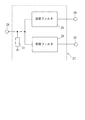
図14aは直列腕を構成する共振器S1〜S4及び並列腕を構成する共振器P1〜P3によりラダー型に組まれた表面弾性波フィルタを示す。この表面弾性波フィルタは、互いに直列接続された共振器S1〜S4の両端に入力ポート13と出力ポート14とを有する。並列腕を構成する共振器P1、P2、P3は、直列腕を構成する共振器S1〜S4どうしを接続するライン15とグランド16との間にそれぞれ挿入される。この構成において、直列腕を構成する共振器S1〜S4のそれぞれに、異なる厚さの圧電層を備えることにより、スプリアス減少の効果が得られる。共振器S1〜S4のうち、2つ以上の共振子の圧電層4の厚さを異ならせてもスプリアス減少の効果が得られる。
FIG. 14a shows a surface elastic wave filter assembled in a ladder shape by resonators S1 to S4 forming series arms and resonators P1 to P3 forming parallel arms. This surface elastic wave filter has an
直列腕を構成する共振器S1〜S4ではなく、並列腕を構成する共振器P1〜P3のすべて又は2つの共振器の圧電層の厚さを異ならせてもスプリアス減少の効果が得られる。直列腕を構成する共振器S1〜S4のうちの2つ以上と、並列腕を構成する共振器P1〜P3の2つ以上のものの圧電層4の厚さを異ならせて構成しても、スプリアス減少の効果が得られる。ラダー型に組まれる共振子S1〜S4及びP1〜P3の数は、用途に応じて任意に変更される。
The effect of reducing spurious can be obtained even if the thickness of the piezoelectric layer of all or two resonators P1 to P3 forming the parallel arm is different from that of the resonators S1 to S4 forming the series arm. Even if two or more of the resonators S1 to S4 forming the series arm and two or more of the resonators P1 to P3 forming the parallel arm are configured with different thicknesses of the
図14bは図14aの変形例の表面弾性波フィルタを示すもので、図14aの共振器S1〜S4、P1〜P3の一部(この例では直列腕の初段の共振器S1)を2つの共振器S11とS12に分割し、これらの共振器S11とS12の圧電層4の厚さを異ならせて、互いに直列に接続したものである。他の共振器S2〜S4、P1〜P3の圧電層4の厚さは同一とする。このように、一部の共振器を分割し、分割した圧電層の厚さを異ならせることにより、共振器S11とS12とで発生するスプリアスを低減することが可能となり、そのスプリアスの影響を低減することができる。共振器S11とS12とは互いに並列接続しても、スプリアスの低減効果が得られる。
FIG. 14b shows a surface elastic wave filter of a modified example of FIG. 14a, and two resonances of a part of the resonators S1 to S4 and P1 to P3 of FIG. 14a (in this example, the first-stage resonator S1 of the series arm). It is divided into vessels S11 and S12, and the thicknesses of the
図14bの表面弾性波フィルタにおいて、他の共振器S2〜S4及びP1〜P3の少なくとも一部においても、それぞれ圧電層4の厚さを異ならせて、互いに直列又は並列に接続して構成しても、スプリアスの影響を低減させることができる。なお、すべての共振器S1〜S4及びP1〜P3をそれぞれ圧電層の厚さが異なる共振器に分割して直列又は並列に接続してもよいが、共振器の分割数を多くすると、共振器で必要とする所要面積が増大するため、設計上の最適化により、共振器の一部のみを分割して直列又は並列に接続することが好ましいこともある。
In the surface elastic wave filter of FIG. 14b, at least a part of the other resonators S2 to S4 and P1 to P3 are also configured by having different thicknesses of the
図15は例えば図3a〜図3d又は図14aもしくは図14bのように構成された本発明による表面弾性波フィルタを用いた受信フィルタ20によるモジュール21の一例を示す。このモジュール21は、異なる複数の送受信信号を扱う移動体通信機器に使用されるものである。このモジュール21は、各周波数対応の本発明による表面弾性波フィルタにより構成される複数の受信フィルタ20と、各受信フィルタ20に対応して設けられたローノイズアンプ(LNA)22と、複数の受信フィルタ20と不図示のアンテナポートとの間に挿入されるスイッチ回路23が含まれる。
FIG. 15 shows an example of the
このモジュール21にも、受信回路を構成する場合に必要となる他の受動素子や回路を含んで構成してもよい。また、モジュール21は、他の回路とを組み合わせにより構成してもよい。
The
図15に示すように、本発明の表面弾性波フィルタ20を用いたモジュール21においても、高域スプリアスが抑制されたモジュール21を実現できる。
As shown in FIG. 15, even in the
図16は本発明による表面弾性波フィルタ用いて構成した送信フィルタ25及び受信フィルタ26を用いたデュプレクサ27の一例を示す。図16に示す送信フィルタ25及び受信フィルタ26は、例えば図3a〜図3dの共振器6A〜6Dを有する表面弾性波フィルタ、又は図14aもしくは図14bように構成された表面弾性波フィルタを用いたものである。このデュプレクサ27は、送信信号の周波数帯と受信信号の周波数帯が近接している移動体通信機器に使用されるものである。送信フィルタ25は不図示のアンテナに接続されるアンテナポート28と、不図示の送信回路に接続される送信回路接続ポート29との間に挿入される。受信フィルタ26はアンテナポート28と、不図示の受信回路に接続される受信回路接続ポート30との間に挿入される。アンテナポート28とグランドとの間は適宜のインピーダンス素子31で接続され、この素子31もデュプレクサ27の一部に含まれる。このように本発明の表面弾性波フィルタを用いてデュプレクサ27を構成することにより、高域スプリアスが抑制されたデュプレクサ27を実現できる。
FIG. 16 shows an example of a
図17は本発明によるデュプレクサ27を用いて構成したモジュール33の一例を示す。このモジュール33は、異なる複数の送受信信号を扱う移動体通信機器に使用されるものである。モジュール33は、図16に示した複数のデュプレクサ27と、各デュプレクサ27にそれぞれ対応して設けられた送信回路34に挿入されたパワーアンプ35と、受信回路36とを含んで構成される。複数のデュプレクサ27と不図示のアンテナポートとの間にスイッチ回路37が挿入され、このスイッチ回路37もモジュール33に含まれる。
FIG. 17 shows an example of the
このモジュール33にも、送受信回路を構成する場合に必要となる他の受動素子や回路を含んで構成してもよい。また、モジュール33は、デュプレクサ27と、パワーアンプ35以外の他の回路とを組み合わせにより構成してもよい。
The
図17に示すように、本発明の表面弾性波フィルタを含むデュプレクサ27を用いたモジュール33においても、高域スプリアスが抑制されたモジュール33を実現できる。
As shown in FIG. 17, even in the
以上、本発明についての説明を行なったが、上述した実施例に限らず、本発明の要旨を逸脱しない範囲において、種々の変更、付加が可能である。 The present invention has been described above, but the present invention is not limited to the above-described embodiment, and various modifications and additions can be made without departing from the gist of the present invention.
1A〜1C…共振子
2…キャリア基板
3…中間層
4…圧電層
5…IDT電極
7…反射器
6A〜6D…共振器
21、33…モジュール
27…デュプレクサ
S1〜S4、S11、S12、P1〜P3…共振器
t1、t2、t3…共振子が配置された領域
1A to 1C ...
Claims (7)
前記キャリア基板は高抵抗の半導体又は絶縁体で構成され、
前記圧電層は、前記IDT電極の電極周期で定まる弾性波の波長をλとしたとき、0.15λ〜1.5λの厚みを有し、
前記キャリア基板上に設けられる前記圧電層は、厚みの異なる複数の領域を備え、
前記複数の領域にそれぞれIDT電極を有する共振子が構成され、
前記複数の領域上にそれぞれ形成された共振子が接続されて構成された共振器を有する表面弾性波フィルタ。 A surface elastic wave filter having a carrier substrate, a piezoelectric layer made of a piezoelectric material provided on the carrier substrate, and a resonator having an IDT electrode formed on the piezoelectric layer.
The carrier substrate is composed of a high resistance semiconductor or an insulator.
The piezoelectric layer has a thickness of 0.15λ to 1.5λ, where λ is the wavelength of the elastic wave determined by the electrode period of the IDT electrode.
The piezoelectric layer provided on the carrier substrate includes a plurality of regions having different thicknesses.
A resonator having an IDT electrode in each of the plurality of regions is configured.
A surface elastic wave filter having a resonator formed by connecting resonators formed on the plurality of regions.
前記圧電層の前記複数の領域の厚さは、ある領域の厚さに対し、次に厚さの小さい領域の厚さが10%以上小さくなるように、段階的な厚さの減少を持たせて設定され、
前記複数の領域上にそれぞれ形成されたIDT電極が直列又は並列に接続された部分を含む、表面弾性波フィルタ。 In the surface elastic wave filter according to claim 1,
The thickness of the plurality of regions of the piezoelectric layer is gradually reduced so that the thickness of the region having the next smallest thickness is reduced by 10% or more with respect to the thickness of a certain region. Set,
A surface elastic wave filter including a portion in which IDT electrodes formed on the plurality of regions are connected in series or in parallel.
前記圧電層で励起される圧電振動の主振動が、SHモードである、表面弾性波フィルタ。 In the surface elastic wave filter according to claim 1 or 2.
A surface elastic wave filter in which the main vibration of the piezoelectric vibration excited by the piezoelectric layer is in SH mode.
前記キャリア基板と前記圧電層との間に、両者の結合の容易化又は弾性波の音速の高速化の少なくともいずれかの役目を果たす1又は複数の中間層を備えた、表面弾性波フィルタ。 In the surface elastic wave filter according to any one of claims 1 to 3,
A surface acoustic wave filter comprising one or a plurality of intermediate layers between the carrier substrate and the piezoelectric layer, which serve at least one of the functions of facilitating the coupling between the two and increasing the speed of sound of a surface acoustic wave.
Priority Applications (2)
| Application Number | Priority Date | Filing Date | Title |
|---|---|---|---|
| JP2019222544A JP7561343B2 (en) | 2019-12-09 | 2019-12-09 | Surface acoustic wave filters, duplexers and modules |
| CN202011421792.1A CN113037244A (en) | 2019-12-09 | 2020-12-08 | Surface acoustic wave filter, duplexer, and module |
Applications Claiming Priority (1)
| Application Number | Priority Date | Filing Date | Title |
|---|---|---|---|
| JP2019222544A JP7561343B2 (en) | 2019-12-09 | 2019-12-09 | Surface acoustic wave filters, duplexers and modules |
Publications (2)
| Publication Number | Publication Date |
|---|---|
| JP2021093609A true JP2021093609A (en) | 2021-06-17 |
| JP7561343B2 JP7561343B2 (en) | 2024-10-04 |
Family
ID=76312859
Family Applications (1)
| Application Number | Title | Priority Date | Filing Date |
|---|---|---|---|
| JP2019222544A Active JP7561343B2 (en) | 2019-12-09 | 2019-12-09 | Surface acoustic wave filters, duplexers and modules |
Country Status (2)
| Country | Link |
|---|---|
| JP (1) | JP7561343B2 (en) |
| CN (1) | CN113037244A (en) |
Cited By (1)
| Publication number | Priority date | Publication date | Assignee | Title |
|---|---|---|---|---|
| WO2024143006A1 (en) * | 2022-12-27 | 2024-07-04 | 株式会社村田製作所 | Elastic wave device |
Families Citing this family (1)
| Publication number | Priority date | Publication date | Assignee | Title |
|---|---|---|---|---|
| CN118432579B (en) * | 2024-06-26 | 2024-11-22 | 深圳飞骧科技股份有限公司 | Notch filter |
Citations (4)
| Publication number | Priority date | Publication date | Assignee | Title |
|---|---|---|---|---|
| WO2016027707A1 (en) * | 2014-08-22 | 2016-02-25 | 株式会社村田製作所 | Ladder filter |
| JP2016072808A (en) * | 2014-09-30 | 2016-05-09 | 株式会社村田製作所 | Duplexer and method of manufacturing the same |
| JP2019047363A (en) * | 2017-09-04 | 2019-03-22 | 株式会社村田製作所 | Elastic wave device, high frequency front end circuit, and communication apparatus |
| WO2019138810A1 (en) * | 2018-01-12 | 2019-07-18 | 株式会社村田製作所 | Elastic wave device, multiplexer, high-frequency front end circuit, and communication device |
Family Cites Families (6)
| Publication number | Priority date | Publication date | Assignee | Title |
|---|---|---|---|---|
| JP5766457B2 (en) * | 2011-02-09 | 2015-08-19 | 太陽誘電株式会社 | Elastic wave device and manufacturing method thereof |
| JP5891049B2 (en) * | 2012-01-31 | 2016-03-22 | スカイワークス・パナソニック フィルターソリューションズ ジャパン株式会社 | Antenna duplexer and its manufacturing method |
| WO2016100692A2 (en) * | 2014-12-17 | 2016-06-23 | Rf Micro Devices, Inc. | Plate wave devices with wave confinement structures and fabrication methods |
| JP2018093487A (en) * | 2016-11-30 | 2018-06-14 | スカイワークス ソリューションズ, インコーポレイテッドSkyworks Solutions, Inc. | Saw filter that comprises piezoelectric substrate having stepwise cross section |
| JP7027144B2 (en) * | 2017-12-07 | 2022-03-01 | 太陽誘電株式会社 | Elastic wave devices and their manufacturing methods and multiplexers |
| JP7169083B2 (en) * | 2018-04-04 | 2022-11-10 | 太陽誘電株式会社 | Acoustic wave devices and multiplexers |
-
2019
- 2019-12-09 JP JP2019222544A patent/JP7561343B2/en active Active
-
2020
- 2020-12-08 CN CN202011421792.1A patent/CN113037244A/en active Pending
Patent Citations (4)
| Publication number | Priority date | Publication date | Assignee | Title |
|---|---|---|---|---|
| WO2016027707A1 (en) * | 2014-08-22 | 2016-02-25 | 株式会社村田製作所 | Ladder filter |
| JP2016072808A (en) * | 2014-09-30 | 2016-05-09 | 株式会社村田製作所 | Duplexer and method of manufacturing the same |
| JP2019047363A (en) * | 2017-09-04 | 2019-03-22 | 株式会社村田製作所 | Elastic wave device, high frequency front end circuit, and communication apparatus |
| WO2019138810A1 (en) * | 2018-01-12 | 2019-07-18 | 株式会社村田製作所 | Elastic wave device, multiplexer, high-frequency front end circuit, and communication device |
Cited By (1)
| Publication number | Priority date | Publication date | Assignee | Title |
|---|---|---|---|---|
| WO2024143006A1 (en) * | 2022-12-27 | 2024-07-04 | 株式会社村田製作所 | Elastic wave device |
Also Published As
| Publication number | Publication date |
|---|---|
| CN113037244A (en) | 2021-06-25 |
| JP7561343B2 (en) | 2024-10-04 |
Similar Documents
| Publication | Publication Date | Title |
|---|---|---|
| JP6959819B2 (en) | Multiplexer | |
| US9819329B2 (en) | Ladder-type surface acoustic wave filter including series and parallel resonators | |
| JP6816834B2 (en) | Elastic wave devices, multiplexers, high frequency front-end circuits, and communication devices | |
| WO2009119007A1 (en) | Surface acoustic wave filter device | |
| US9847770B2 (en) | Elastic wave resonator, elastic wave filter apparatus, and duplexer | |
| WO2015080045A1 (en) | Splitter | |
| JP2017153132A (en) | Ladder type elastic wave filter and antenna duplexer using the same | |
| JP7004009B2 (en) | Elastic wave devices, multiplexers, high frequency front-end circuits, and communication devices | |
| JP2014039199A (en) | Acoustic wave filter, duplexer and module | |
| JP2017034363A (en) | Acoustic wave devices and modules | |
| US20230261633A1 (en) | Layered temperature-compensated surface acoustic wave resonator and packaging method | |
| JPWO2007007476A1 (en) | Boundary wave filter device | |
| CN111937305A (en) | Elastic wave element, elastic wave filter, branching filter, and communication device | |
| WO2021015187A1 (en) | Elastic wave filter | |
| JPWO2020036100A1 (en) | SAW filter | |
| US11979139B2 (en) | Elastic wave device, elastic waves filter, duplexer, and module | |
| JP7561343B2 (en) | Surface acoustic wave filters, duplexers and modules | |
| WO2000070758A1 (en) | Surface acoustic wave device | |
| JP2021122090A (en) | Acoustic wave filter | |
| JP2014160888A (en) | Acoustic wave resonator, acoustic wave filter using the same and antenna duplexer | |
| JP2020043386A (en) | Ladder type filter and multiplexer | |
| JP7510417B2 (en) | Acoustic wave device, high frequency front-end circuit and communication device | |
| JPWO2005036743A1 (en) | Boundary acoustic wave device | |
| JPH09121136A (en) | Ladder surface acoustic wave filter for resonator | |
| JP2006129057A (en) | Surface acoustic wave device |
Legal Events
| Date | Code | Title | Description |
|---|---|---|---|
| A621 | Written request for application examination |
Free format text: JAPANESE INTERMEDIATE CODE: A621 Effective date: 20221206 |
|
| A521 | Request for written amendment filed |
Free format text: JAPANESE INTERMEDIATE CODE: A523 Effective date: 20221209 |
|
| A977 | Report on retrieval |
Free format text: JAPANESE INTERMEDIATE CODE: A971007 Effective date: 20231003 |
|
| A131 | Notification of reasons for refusal |
Free format text: JAPANESE INTERMEDIATE CODE: A131 Effective date: 20231107 |
|
| A521 | Request for written amendment filed |
Free format text: JAPANESE INTERMEDIATE CODE: A523 Effective date: 20240105 |
|
| A131 | Notification of reasons for refusal |
Free format text: JAPANESE INTERMEDIATE CODE: A131 Effective date: 20240402 |
|
| A521 | Request for written amendment filed |
Free format text: JAPANESE INTERMEDIATE CODE: A523 Effective date: 20240603 |
|
| TRDD | Decision of grant or rejection written | ||
| A01 | Written decision to grant a patent or to grant a registration (utility model) |
Free format text: JAPANESE INTERMEDIATE CODE: A01 Effective date: 20240814 |
|
| A61 | First payment of annual fees (during grant procedure) |
Free format text: JAPANESE INTERMEDIATE CODE: A61 Effective date: 20240911 |
|
| R150 | Certificate of patent or registration of utility model |
Ref document number: 7561343 Country of ref document: JP Free format text: JAPANESE INTERMEDIATE CODE: R150 |