[go: up one dir, main page]

JP2020031423A - Signal generation device - Google Patents

Signal generation device Download PDF

Info

Publication number
JP2020031423A
JP2020031423A JP2019133206A JP2019133206A JP2020031423A JP 2020031423 A JP2020031423 A JP 2020031423A JP 2019133206 A JP2019133206 A JP 2019133206A JP 2019133206 A JP2019133206 A JP 2019133206A JP 2020031423 A JP2020031423 A JP 2020031423A
Authority
JP
Japan
Prior art keywords
voltage
signal
pair
circuit
peak
Prior art date
Legal status (The legal status is an assumption and is not a legal conclusion. Google has not performed a legal analysis and makes no representation as to the accuracy of the status listed.)
Granted
Application number
JP2019133206A
Other languages
Japanese (ja)
Other versions
JP7237759B2 (en
Inventor
浩一 柳沢
Koichi Yanagisawa
浩一 柳沢
大佳 池田
Hiroyoshi Ikeda
大佳 池田
真 笠井
Makoto Kasai
真 笠井
智春 坂井
Tomoharu Sakai
智春 坂井
Current Assignee (The listed assignees may be inaccurate. Google has not performed a legal analysis and makes no representation or warranty as to the accuracy of the list.)
Hioki EE Corp
Original Assignee
Hioki EE Corp
Priority date (The priority date is an assumption and is not a legal conclusion. Google has not performed a legal analysis and makes no representation as to the accuracy of the date listed.)
Filing date
Publication date
Application filed by Hioki EE Corp filed Critical Hioki EE Corp
Publication of JP2020031423A publication Critical patent/JP2020031423A/en
Application granted granted Critical
Publication of JP7237759B2 publication Critical patent/JP7237759B2/en
Active legal-status Critical Current
Anticipated expiration legal-status Critical

Links

Images

Landscapes

  • Dc Digital Transmission (AREA)

Abstract

【課題】シリアルバスに伝送されているCANフレームを特定可能な符号特定用信号を生成して、LVDSで出力する。【解決手段】CAN通信路(シリアルバスSB)を構成する一対の被覆導線La,Lbに一対のプローブPLa,PLbを介して接続されて、シリアルバスSBを介して伝送される2線差動電圧方式のロジック信号(被覆導線La,Lbに伝送される各電圧信号の電圧Va,Vbの電位差(Va−Vb)である差動信号)に基づき、このロジック信号に対応する符号を特定可能な符号特定用信号Sfを生成する。また、符号特定用信号SfをLVDS信号Vfに変換して外部に出力するLVDSドライバ6を備えている。【選択図】図1A code identification signal capable of identifying a CAN frame being transmitted over a serial bus is generated and output by LVDS. A two-wire differential voltage is connected via a pair of probes PLa and PLb to a pair of covered conductors La and Lb that constitute a CAN communication path (serial bus SB) and is transmitted via the serial bus SB. A code that can identify the code corresponding to this logic signal based on the logic signal of the system (the differential signal that is the potential difference (Va-Vb) between the voltages Va and Vb of the voltage signals transmitted to the coated conductors La and Lb) A specifying signal Sf is generated. It also has an LVDS driver 6 that converts the code specifying signal Sf into an LVDS signal Vf and outputs it to the outside. [Selection drawing] Fig. 1

Description

本発明は、通信路を介して伝送される2線差動電圧方式のロジック信号に基づいてロジック信号に対応する符号を特定可能な符号特定用信号を生成する信号生成装置に関するものである。   The present invention relates to a signal generation device that generates a code specifying signal capable of specifying a code corresponding to a logic signal based on a logic signal of a two-wire differential voltage system transmitted via a communication path.

例えば、下記の特許文献1には、CAN通信用のシリアルバス(車内LAN)を介して伝送されている各種CANフレーム(制御データ)を収集して記録可能に構成された車両データ収集装置(以下、単に「収集装置」ともいう)の発明が開示されている。この収集装置は、故障診断やメンテナンスなどを目的として外部機器を接続可能にシリアルバスに設けられているダイアグコネクタ(診断機器接続用コネクタ:以下、単に「コネクタ」ともいう)に接続可能に構成されている。また、この収集装置では、上記のコネクタに接続することでコネクタを介して供給される電源によって動作し、イグニッションスイッチの操作に連動してシリアルバスからのCANフレームの収集の開始/停止を自動的に実行する構成が採用されている。   For example, Patent Literature 1 below discloses a vehicle data collection device (hereinafter referred to as a vehicle data collection device) configured to collect and record various CAN frames (control data) transmitted via a serial bus (in-vehicle LAN) for CAN communication. , Also simply referred to as “collection device”). This collection device is configured to be connectable to a diagnostic connector (connector for diagnostic device connection: hereinafter simply referred to as a “connector”) provided on a serial bus so that external devices can be connected for the purpose of failure diagnosis and maintenance. ing. In addition, in this collecting device, when connected to the connector, the collecting device operates by a power supply supplied through the connector, and automatically starts / stops collecting CAN frames from the serial bus in conjunction with operation of an ignition switch. Is executed.

特開2008−70133号公報(第4−11頁、第1−17図)JP 2008-70133 A (Page 4-11, FIG. 1-17)

ところが、上記特許文献に開示の収集装置には、以下のような解決すべき課題が存在している。具体的には、上記の収集装置では、コネクタを介して接続したシリアルバスから各種のCANフレーム(2線差動電圧方式のロジック信号によって示されている符号の列)を収集する構成であることから、CANの通信プロトコル(CANプロトコル)に準拠した信号を入力する入力仕様が標準仕様となっている。しかしながら、CANの入力規格以外の入力規格(特に、LVDS(Low Voltage Differential Signaling)規格に準拠した入力規格)に適合した信号を入力する収集装置が既に多く存在しており、これらの収集装置をCANフレーム(または、ロジック信号によって示されている符号を特定可能な符号特定用信号)の収集に利用できれば便利である。   However, the collecting device disclosed in the above-mentioned patent document has the following problems to be solved. Specifically, the above-described collecting device is configured to collect various CAN frames (a sequence of codes indicated by a logic signal of a two-wire differential voltage system) from a serial bus connected via a connector. Thus, an input specification for inputting a signal conforming to a CAN communication protocol (CAN protocol) has become a standard specification. However, there are already many collecting devices for inputting a signal conforming to an input standard other than the CAN input standard (particularly, an input standard conforming to the LVDS (Low Voltage Differential Signaling) standard). It is convenient if it can be used for collecting a frame (or a code specifying signal capable of specifying a code indicated by a logic signal).

なお、自動車に搭載されているCAN通信用のシリアルバス(通信路)における課題について例示したが、自動車以外の分野(例えば、工場内に設置される機械設備の分野)においても、複数の機械設備がノードとして接続されたCAN通信用のシリアルバス(通信路)が使用されており、このシリアルバスを介して伝送されているCANフレーム(または、ロジック信号によって示されている符号を特定可能な符号特定用信号)の収集に際しても、CANの入力規格以外の入力規格(特に、LVDS規格に準拠した入力規格)に適合した信号(特にLVDS)を入力する収集装置を利用できれば便利である。   Although the problem in the serial bus (communication path) for CAN communication mounted on an automobile has been exemplified, a plurality of mechanical facilities may be used in a field other than the automobile (for example, a field of a mechanical facility installed in a factory). Is used as a CAN communication serial bus (communication path) connected as a node, and a CAN frame transmitted through the serial bus (or a code capable of specifying a code indicated by a logic signal) is used. It is convenient when collecting a signal (specifically, LVDS) that is compatible with an input standard other than the CAN input standard (particularly, an input standard conforming to the LVDS standard).

本発明は、かかる解決すべき課題に鑑みてなされたものであり、CAN通信用のシリアルバスを介して伝送されているCANフレーム(CANフレームを構成する符号)を特定可能な符号特定用信号を生成すると共にLVDSで出力可能とする信号生成装置を提供することを主目的とする。   The present invention has been made in view of such a problem to be solved, and provides a code specifying signal that can specify a CAN frame (a code forming a CAN frame) transmitted via a serial bus for CAN communication. A main object of the present invention is to provide a signal generation device that can generate and output the data using LVDS.

上記目的を達成すべく請求項1記載の信号生成装置は、CAN通信路を構成する一対の信号線に一対のプローブを介して接続されて、当該CAN通信路を介して伝送される2線差動電圧方式のロジック信号に基づき、当該ロジック信号に対応する符号を特定可能な符号特定用信号を生成する信号生成装置であって、前記符号特定用信号をLVDSに変換して外部に出力するLVDSドライバを備えている。   In order to achieve the above object, the signal generating device according to claim 1 is connected to a pair of signal lines constituting a CAN communication path via a pair of probes and transmitted through the CAN communication path. What is claimed is: 1. A signal generating device for generating a code specifying signal capable of specifying a code corresponding to a logic signal based on a dynamic voltage type logic signal, comprising: converting the code specifying signal into LVDS and outputting the LVDS to the outside It has a driver.

また、請求項2記載の信号生成装置は、請求項1記載の信号生成装置において、前記一対のプローブのうちの一方のプローブを含んで構成されて、前記一対の信号線のうちの当該一方のプローブを介して接続された一方の信号線に伝送されている電圧に応じて電圧が変化する第1電圧信号を発生させる第1ハイインピーダンス回路と、前記一対のプローブのうちの他方のプローブを含んで構成されて、前記一対の信号線のうちの当該他方のプローブを介して接続された他方の信号線に伝送されている電圧に応じて電圧が変化する第2電圧信号を発生させる第2ハイインピーダンス回路と、前記第1電圧信号および前記第2電圧信号を入力すると共に当該各電圧信号の差分電圧に応じて電圧が変化する差分信号を出力する差動増幅回路と、前記差分信号を、当該差分信号の交流成分のピークピーク電圧と同等のピークピーク電圧で、かつ低電圧期間の電圧がターゲット定電圧に規定されたシングルエンド信号に整形して出力する波形整形回路とを備えて、当該シングルエンド信号に基づいて前記符号特定用信号を生成する。   Further, the signal generation device according to claim 2 is the signal generation device according to claim 1, wherein the signal generation device includes one of the pair of probes and includes the one of the pair of signal lines. A first high-impedance circuit that generates a first voltage signal whose voltage changes in accordance with a voltage transmitted to one of the signal lines connected via the probe, and the other of the pair of probes And a second high signal that generates a second voltage signal whose voltage changes in accordance with the voltage transmitted to the other signal line of the pair of signal lines connected via the other probe. An impedance circuit, a differential amplifier circuit that receives the first voltage signal and the second voltage signal and outputs a differential signal whose voltage changes according to a differential voltage between the voltage signals; A waveform shaping circuit for shaping the minute signal into a single-ended signal having a peak-to-peak voltage equivalent to the peak-to-peak voltage of the AC component of the differential signal, and a voltage in a low voltage period specified as a target constant voltage, and outputting the signal. And generating the code specifying signal based on the single-ended signal.

また、請求項3記載の信号生成装置は、請求項1記載の信号生成装置において、前記一対のプローブのうちの一方のプローブを含んで構成されて、前記一対の信号線のうちの当該一方のプローブを介して接続された一方の信号線に伝送されている電圧に応じて電圧が変化する第1電圧信号を発生させる第1ハイインピーダンス回路と、前記一対のプローブのうちの他方のプローブを含んで構成されて、前記一対の信号線のうちの当該他方のプローブを介して接続された他方の信号線に伝送されている電圧に応じて電圧が変化する第2電圧信号を発生させる第2ハイインピーダンス回路と、前記第1電圧信号および前記第2電圧信号を入力すると共に当該各電圧信号の差分電圧に応じて電圧が変化する差分信号を出力する差動増幅回路と、前記差分信号を、当該差分信号の交流成分のピークピーク電圧と同等のピークピーク電圧で、かつ高電圧期間の電圧がターゲット定電圧に規定されたシングルエンド信号に整形して出力する波形整形回路とを備えて、当該シングルエンド信号に基づいて前記符号特定用信号を生成する。   The signal generating device according to a third aspect is the signal generating device according to the first aspect, wherein the signal generating device includes one of the pair of probes and includes the one of the pair of signal lines. A first high-impedance circuit that generates a first voltage signal whose voltage changes in accordance with a voltage transmitted to one of the signal lines connected via the probe, and the other of the pair of probes And a second high signal that generates a second voltage signal whose voltage changes in accordance with the voltage transmitted to the other signal line of the pair of signal lines connected via the other probe. An impedance circuit, a differential amplifier circuit that receives the first voltage signal and the second voltage signal and outputs a differential signal whose voltage changes according to a differential voltage between the voltage signals; A waveform shaping circuit for shaping the minute signal into a single-ended signal having a peak-to-peak voltage equivalent to the peak-to-peak voltage of the AC component of the differential signal, and a voltage in a high voltage period specified as a target constant voltage, and outputting the signal. And generating the code specifying signal based on the single-ended signal.

また、請求項4記載の信号生成装置は、請求項2または3記載の信号生成装置において、前記シングルエンド信号を閾値電圧と比較して二値化することにより前記符号特定用信号を生成する信号生成部を備えている。   According to a fourth aspect of the present invention, in the signal generation apparatus according to the second or third aspect, the signal for generating the code specifying signal by binarizing the single-ended signal by comparing the single-ended signal with a threshold voltage. A generation unit is provided.

また、請求項5記載の信号生成装置は、請求項1から4のいずれかに記載の信号生成装置において、前記一対の信号線は、被覆導線でそれぞれ構成され、前記一対のプローブは、対応する被覆導線における被覆部に接触させられて、当該被覆導線と容量結合する電極をそれぞれ備えている。   According to a fifth aspect of the present invention, in the signal generating device according to any one of the first to fourth aspects, the pair of signal lines are each configured by a covered conductor, and the pair of probes correspond to each other. An electrode is provided which is brought into contact with the covering portion of the covered conductor and is capacitively coupled to the covered conductor.

また、請求項6記載の信号生成装置は、請求項1から4のいずれかに記載の信号生成装置において、前記一対のプローブは、前記一対の信号線のうちの対応する信号線に装着されて、当該信号線に流れる電流であって、当該信号線に伝送されている電圧に応じて電流値が変化する電流を検出すると共に、当該電流値に応じて電圧値が変化する電圧信号をそれぞれ出力する一対の電流検出プローブで構成されている。   According to a sixth aspect of the present invention, in the signal generating apparatus according to any one of the first to fourth aspects, the pair of probes are mounted on corresponding signal lines of the pair of signal lines. Detecting a current flowing through the signal line, the current value changing according to the voltage transmitted to the signal line, and outputting a voltage signal changing a voltage value according to the current value, And a pair of current detection probes.

請求項1記載の信号生成装置によれば、CAN通信用の一対の信号線を介して伝送されているロジック信号に対応する符号を特定可能な符号特定用信号を生成すると共にLVDSに変換して出力するため、既に多く存在しているLVDS対応機器(収集装置など)を使用してロジック信号についての各種の処理を実行することができるため、極めて有用で便利となる。   According to the signal generation device of the first aspect, a code specifying signal capable of specifying a code corresponding to a logic signal transmitted through a pair of signal lines for CAN communication is generated and converted into LVDS. Since the output is performed, various processes for the logic signal can be executed using an LVDS-compatible device (collection device or the like) that already exists, which is extremely useful and convenient.

請求項2,3記載の信号生成装置によれば、第1ハイインピーダンス回路を介して一方の信号線に接続されると共に、第2ハイインピーダンス回路を介して他方の信号線に接続されるため、一対の信号線に伝送されている電圧に対して殆ど影響を与えることなく、この電圧を検出して符号特定用信号を生成し、LVDSに変換して外部のLVDS対応機器に出力することができる。   According to the signal generation device of the second and third aspects, the signal generation device is connected to one signal line via the first high impedance circuit, and is connected to the other signal line via the second high impedance circuit. The voltage transmitted to the pair of signal lines is hardly affected, and this voltage is detected, a code specifying signal is generated, converted to LVDS, and output to an external LVDS-compatible device. .

請求項4記載の信号生成装置によれば、波形整形回路の後段に配置された信号生成部が、ターゲット定電圧を基準として規定された閾値電圧と比較することで、シングルエンド信号を確実に二値化して(一定振幅の信号にして)符号特定用信号を生成することができる。   According to the signal generation device of the fourth aspect, the signal generation unit disposed at the subsequent stage of the waveform shaping circuit compares the single-ended signal with the threshold voltage defined on the basis of the target constant voltage, thereby reliably generating the single-ended signal. It is possible to generate a code specifying signal by converting the value (to a signal having a constant amplitude).

請求項5記載の信号生成装置によれば、一対のプローブに、対応する被覆導線における被覆部に接触させられて、被覆導線と容量結合する電極がそれぞれ備えられているため、一対の被覆導線における長手方向の任意の部位にプローブを接続する(つまり、被覆導線の任意の部位の被覆部に電極を接触させる)簡易な作業を行うことで、一対の信号線を介して伝送されているロジック信号によって示されている符号を特定可能な符号特定用信号を生成すると共にLVDSに変換して外部に出力することができる。   According to the signal generation device of the fifth aspect, since the pair of probes are provided with the electrodes that are brought into contact with the covering portions of the corresponding covered conductors and that are capacitively coupled to the covered conductors, respectively. By performing a simple operation of connecting a probe to an arbitrary portion in the longitudinal direction (that is, bringing an electrode into contact with a coating portion of an arbitrary portion of a coated conductor), a logic signal transmitted through a pair of signal lines is performed. Can generate a code specifying signal that can specify the code indicated by (1), and can convert the code into LVDS and output it to the outside.

請求項6記載の信号生成装置によれば、一対のプローブがそれぞれ電流検出プローブで構成されているため、一対の信号線における長手方向の任意の部位にプローブを接続する(つまり、信号線の任意の部位にプローブを装着する)簡易な作業を行うことで、一対の信号線を介して伝送されているロジック信号によって示されている符号を特定可能な符号特定用信号を生成すると共にLVDSに変換して外部に出力することができる。   According to the signal generating device of the sixth aspect, since each of the pair of probes is constituted by the current detection probe, the probe is connected to an arbitrary portion in the longitudinal direction of the pair of signal lines (that is, an arbitrary portion of the signal line). A simple operation is performed to generate a code specifying signal capable of specifying a code indicated by a logic signal transmitted through a pair of signal lines and to convert the code to LVDS. And output it to the outside.

信号生成装置1の構成を示すブロック図である。FIG. 2 is a block diagram illustrating a configuration of the signal generation device 1. 信号生成装置1の構成の一例を示す構成図である。FIG. 2 is a configuration diagram illustrating an example of a configuration of a signal generation device. 差動増幅回路41の他の構成を示す回路図である。FIG. 9 is a circuit diagram illustrating another configuration of the differential amplifier circuit 41. 差動増幅回路41の他の構成を示す回路図である。FIG. 9 is a circuit diagram illustrating another configuration of the differential amplifier circuit 41. 図2の波形整形回路42の構成、および信号生成部5の構成を示す回路図である。FIG. 3 is a circuit diagram showing a configuration of a waveform shaping circuit 42 in FIG. 2 and a configuration of a signal generation unit 5. 図5の波形整形回路42および信号生成部5を備えた信号生成装置1の動作を説明するための波形図である。FIG. 6 is a waveform chart for explaining an operation of the signal generation device 1 including the waveform shaping circuit 42 and the signal generation unit 5 of FIG. 5. 波形整形回路42の他の構成、および信号生成部5の他の構成を示す回路図である。FIG. 9 is a circuit diagram illustrating another configuration of the waveform shaping circuit and another configuration of the signal generation unit. 図7の波形整形回路42および信号生成部5を備えた信号生成装置1の動作を説明するための波形図である。FIG. 8 is a waveform chart for explaining an operation of the signal generation device 1 including the waveform shaping circuit 42 and the signal generation unit 5 of FIG. 7. プローブPLの他の構成を示す構成図である。FIG. 11 is a configuration diagram illustrating another configuration of a probe PL. 図5のスイッチ42fを負論理で動作する構成としたときの波形整形回路42の回路図である。FIG. 6 is a circuit diagram of a waveform shaping circuit when the switch of FIG. 5 is configured to operate with negative logic. 図7のスイッチ42fを負論理で動作する構成としたときの波形整形回路42の回路図である。FIG. 8 is a circuit diagram of the waveform shaping circuit 42 when the switch 42f of FIG. 7 operates in negative logic. 図5の第4インピーダンス素子42eを削除した構成の波形整形回路42の回路図である。FIG. 6 is a circuit diagram of a waveform shaping circuit having a configuration in which a fourth impedance element shown in FIG. 5 is omitted. 図7の第4インピーダンス素子42eを削除した構成の波形整形回路42の回路図である。FIG. 8 is a circuit diagram of a waveform shaping circuit 42 having a configuration in which a fourth impedance element 42e in FIG. 7 is deleted. 信号生成装置1を被覆導線La,Lbに接続する構成を説明するための構成図である。FIG. 2 is a configuration diagram for describing a configuration in which the signal generation device 1 is connected to covered conductors La and Lb. 信号生成装置1を被覆導線La,Lbに接続する他の構成を説明するための構成図である。FIG. 6 is a configuration diagram for explaining another configuration for connecting the signal generation device 1 to the covered conductors La and Lb. 信号生成装置1を電流検出プローブPLc,PLdで被覆導線La,Lbに接続する構造を説明するための構成図である。FIG. 2 is a configuration diagram for describing a structure in which the signal generation device 1 is connected to covered conductors La and Lb by current detection probes PLc and PLd.

以下、信号生成装置の実施の形態について、添付図面を参照して説明する。   Hereinafter, an embodiment of a signal generation device will be described with reference to the accompanying drawings.

図1,2に示す信号生成装置1は、「信号生成装置」の一例であって、第1インピーダンス素子2、第2インピーダンス素子3、差動増幅部4、信号生成部5、LVDSドライバ6および出力コネクタ7(または出力ケーブル)を備えて構成されている。この信号生成装置1は、自動車に配設されているCAN通信用のシリアルバスSB(「CAN通信路」の一例)からCANフレーム(「CAN通信路を介して伝送される2線差動電圧方式のロジック信号」の一例)を読み取り、読み取ったCANフレームと同じCANフレームCsを示すLVDS(後述するLVDS信号Vf)を各種のLVDS対応機器(収集装置など)に出力することができるように(CAN−LVDS変換器として)構成されている。なお、シリアルバスSBは、それぞれ被覆導線で構成された一対の信号線(高電位側信号線(CANH)と低電位側信号線(CANL))で構成されている。   The signal generation device 1 illustrated in FIGS. 1 and 2 is an example of a “signal generation device”, and includes a first impedance element 2, a second impedance element 3, a differential amplifier 4, a signal generator 5, an LVDS driver 6, An output connector 7 (or an output cable) is provided. The signal generating device 1 is configured to transmit a CAN frame (“2-wire differential voltage system transmitted via a CAN communication path”) from a CAN communication serial bus SB (an example of a “CAN communication path”) provided in an automobile. ), And outputs an LVDS (LVDS signal Vf to be described later) indicating the same CAN frame Cs as the read CAN frame to various LVDS-compatible devices (such as a collecting device). -As an LVDS converter). The serial bus SB is composed of a pair of signal lines (high-potential-side signal line (CANH) and low-potential-side signal line (CANL)) each composed of a coated conductor.

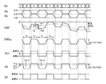
この場合、シリアルバスSBを介してのCANプロトコルに準拠した通信時には、図2に示すように、CANフレーム(符号列)を構成する各符号を表すロジック信号Saが、シリアルバスSBにおける2本の信号線のうちのCANHigh(CANH)の信号線としての被覆導線Laに伝送される電圧信号の電圧Va(以下、理解の容易のため、この電圧信号自体を電圧信号Vaともいう)と、2本の信号線のうちのCANLow(CANL)の信号線としての被覆導線Lbに伝送される電圧信号の電圧Vb(以下、理解の容易のため、この電圧信号自体を電圧信号Vbともいう)との間の電位差(Va−Vb)である差動信号として伝送される。信号生成装置1は、このロジック信号Sa(具体的には、電圧信号Va,Vbに基づき、図6に示すように、電圧信号Va,Vbに対応する符号Cs(電位差(Va−Vb)である差動信号に対応する符号Cs(「1」または「0」)))を特定可能な符号特定用信号Sfを生成すると共に、LVDS信号Vfに変換して装置外部に出力する。   In this case, at the time of communication conforming to the CAN protocol via the serial bus SB, as shown in FIG. 2, a logic signal Sa representing each code constituting the CAN frame (code string) is transmitted by two lines on the serial bus SB. Two voltage signals Va (hereinafter also referred to as a voltage signal Va itself for easy understanding) of a voltage signal transmitted to the covered conductor La as a signal line of CANHHigh (CANH) among the signal lines. Between the voltage signal Vb of the voltage signal transmitted to the covered conductor Lb as the signal line of CANLow (CANL) (hereinafter, also referred to as the voltage signal Vb for easy understanding). Is transmitted as a differential signal which is a potential difference (Va−Vb). The signal generation device 1 uses the logic signal Sa (specifically, based on the voltage signals Va and Vb, as shown in FIG. 6, a code Cs (potential difference (Va−Vb) corresponding to the voltage signals Va and Vb). A code specifying signal Sf that can specify the code Cs (“1” or “0”)) corresponding to the differential signal is generated, and is converted into an LVDS signal Vf and output to the outside of the device.

なお、シリアルバスSBを介してのロジック信号Saの伝送原理については公知のため、詳細な説明を省略するが、CANHigh(CANH)の電圧信号VaおよびCANLow(CANL)の電圧信号Vbの仕様について簡単に説明する。図6に示すように、電圧信号Va,Vbは、ベースになる電圧(+2.5V)から逆方向に変化する電圧信号であって、電圧信号Vaがこのベースの電圧のときには、電圧信号Vbも同じ期間に亘り同じベースの電圧になって、電位差(Va−Vb)がゼロ(最小)となるこの期間に伝送されるCANフレームを構成する符号Cs(論理値)は「1」を示すものとなる。一方、電圧信号Vaがこのベースの電圧よりも高電圧の規定電圧(+3.5V)のときには、電圧信号Vbは同じ期間に亘り、逆にベースの電圧よりも低電圧の他の規定電圧(+1.5V)になって、電位差(Va−Vb)が最大となるこの期間に伝送されるCANフレームを構成する符号Cs(論理値)は「0」を示すものとなる。また、シリアルバスSBにおいて差動信号を伝送するための基準電位となる信号線である「SG」や、差動信号の伝送の用途以外に配設されている信号線および電力線等の図示および説明を省略する。   Since the principle of transmission of the logic signal Sa via the serial bus SB is publicly known, a detailed description is omitted, but the specifications of the voltage signal Va of CANHHigh (CANH) and the voltage signal Vb of CANLow (CANL) will be briefly described. Will be described. As shown in FIG. 6, the voltage signals Va and Vb are voltage signals that change in the opposite direction from the base voltage (+2.5 V). When the voltage signal Va is the base voltage, the voltage signal Vb is also changed. The code Cs (logical value) constituting the CAN frame transmitted during this period in which the voltage of the same base becomes the same over the same period and the potential difference (Va−Vb) becomes zero (minimum) indicates “1”. Become. On the other hand, when the voltage signal Va is a specified voltage (+3.5 V) higher than the base voltage, the voltage signal Vb is set to the other specified voltage (+1 .5 V), the code Cs (logical value) constituting the CAN frame transmitted during this period in which the potential difference (Va−Vb) is the maximum indicates “0”. In addition, illustration and description of “SG” which is a signal line serving as a reference potential for transmitting a differential signal on the serial bus SB, and a signal line and a power line provided for purposes other than transmission of the differential signal Is omitted.

信号生成装置1は、図1,2に示すように、一対のプローブPLa,PLb(特に区別しないときには、プローブPLともいう)を介して被覆導線La,Lb(特に区別しないときには、被覆導線Lともいう)に接続される。一例として、プローブPLaは、電極部11aおよびシールドケーブル(同軸ケーブル)CBaを備えて構成されて、第1インピーダンス素子2に接続される。プローブPLbは、電極部11bおよびシールドケーブル(同軸ケーブル)CBbを備えてプローブPLaとは別体に構成されて、第2インピーダンス素子3に接続される。   As shown in FIGS. 1 and 2, the signal generation device 1 includes a pair of probes PLa and PLb (also referred to as a probe PL when not particularly distinguished) and covered wires La and Lb (when not particularly distinguished, also includes a covered wire L). Connected). As an example, the probe PLa includes an electrode portion 11a and a shielded cable (coaxial cable) CBa, and is connected to the first impedance element 2. The probe PLb includes an electrode portion 11b and a shielded cable (coaxial cable) CBb, is configured separately from the probe PLa, and is connected to the second impedance element 3.

電極部11a,11bは、電極21およびシールド22を備えて同一に構成されている。また、各電極部11a,11bは、被覆導線La,Lbのうちの任意の一方に対して着脱可能に構成されている。なお、理解の容易のため、図1,2に示すように、電極部11aは被覆導線Laに装着され、電極部11bは被覆導線Lbに装着されるものとする。また、電極部11a,11bは、対応する被覆導線Lへの装着状態において、その被覆導線Lの絶縁被覆部(以下、単に「被覆部」ともいう)に電極21が接触(当接)するように構成されている。この構成により、電極部11a,11bの各電極21は、対応する被覆導線La,Lbの金属部(芯線)と接触することなく非接触の状態(つまり、金属非接触の状態)で容量結合する。なお、この結合容量の容量値は、一般的に数pF程度の小容量値である。また、シールド22は、各電極部11a,11bが対応する被覆導線La,Lbに装着されている状態において、被覆導線La,Lbの被覆部における電極21の接触部位を、この電極21を含めて覆うことで、電極21が対応する被覆導線Laの金属部以外の金属部と容量結合することを防止する。   The electrode portions 11a and 11b have the same configuration including the electrode 21 and the shield 22. Each of the electrode portions 11a and 11b is configured to be detachable from any one of the covered conductors La and Lb. For easy understanding, it is assumed that the electrode portion 11a is attached to the covered conductor La and the electrode portion 11b is attached to the covered conductor Lb, as shown in FIGS. Further, the electrodes 21a and 11b are arranged such that the electrode 21 contacts (contacts) an insulating coating portion (hereinafter, also simply referred to as a “covering portion”) of the coating conductor L when the electrode portion 11a and 11b are attached to the corresponding coating conductor L. Is configured. With this configuration, the electrodes 21 of the electrode portions 11a and 11b are capacitively coupled in a non-contact state (that is, a metal non-contact state) without contacting the metal portions (core wires) of the corresponding covered conductors La and Lb. . The capacitance value of the coupling capacitance is generally a small capacitance value of about several pF. Further, in a state where each of the electrode portions 11a and 11b is attached to the corresponding covered conductors La and Lb, the shield 22 includes the contact portions of the electrodes 21 in the covering portions of the covered conductors La and Lb including the electrodes 21. The covering prevents the electrode 21 from being capacitively coupled to a metal part other than the metal part of the corresponding covered conductor La.

したがって、信号生成装置1では、被覆導線La,Lbの金属部(芯線)と電極部11a,11bの各電極21との間に形成される各結合容量は、被覆導線La,Lbと信号生成装置1側の電子回路とを直流的に絶縁するガルバニック絶縁回路として機能して、被覆導線La,Lbに重畳する虞のある直流電圧の信号生成装置1への印加を回避して、安全性を高めることが可能となっている。   Therefore, in the signal generation device 1, each coupling capacitance formed between the metal portion (core wire) of the covered conductors La and Lb and each electrode 21 of the electrode portions 11a and 11b is equal to the capacitance of the covered conductors La and Lb and the signal generation device. It functions as a galvanic insulation circuit that insulates the electronic circuit on the first side in a DC manner, and avoids applying a DC voltage, which may be superimposed on the covered conductors La and Lb, to the signal generation device 1 to enhance safety. It has become possible.

第1インピーダンス素子2は、本例では一例として、図2に示すように、抵抗31a、および抵抗31aに並列接続されたコンデンサ32aを備えて構成され、また第2インピーダンス素子3は、抵抗31b(抵抗31aと同じ抵抗値)、および抵抗31bに並列接続されたコンデンサ32b(コンデンサ32aと同じ容量値)を備えて構成されている。第1インピーダンス素子2では、抵抗31aは、高抵抗値の抵抗(少なくとも数MΩ程度の高(ハイ)インピーダンス抵抗)で構成されて、その一端(第1インピーダンス素子2の一端)がプローブPLaを構成するシールドケーブルCBaの芯線を介して電極部11aの電極21に接続されると共に後述する差動増幅回路41の入力段に配設された演算増幅器41aの入力端子(非反転入力端子)に接続され、その他端(第1インピーダンス素子2の他端)が信号生成装置1における基準電位の部位(グランドG)に接続されている。   As shown in FIG. 2, the first impedance element 2 includes, for example, a resistor 31a and a capacitor 32a connected in parallel with the resistor 31a, and the second impedance element 3 includes a resistor 31b ( It has the same resistance value as the resistor 31a) and a capacitor 32b (the same capacitance value as the capacitor 32a) connected in parallel to the resistor 31b. In the first impedance element 2, the resistor 31a is configured by a resistor having a high resistance value (at least a high (high) impedance resistance of about several MΩ), and one end (one end of the first impedance element 2) configures the probe PLa. Connected to the electrode 21 of the electrode portion 11a via the core wire of the shielded cable CBa to be connected, and to the input terminal (non-inverting input terminal) of the operational amplifier 41a disposed at the input stage of the differential amplifier circuit 41 described later. The other end (the other end of the first impedance element 2) is connected to a reference potential portion (ground G) in the signal generating device 1.

また、第2インピーダンス素子3では、抵抗31bは、高抵抗値の抵抗(高インピーダンス抵抗)で構成されて、その一端(第2インピーダンス素子3の一端)がプローブPLbを構成するシールドケーブルCBbの芯線を介して電極部11bの電極21に接続されると共に後述する差動増幅回路41の入力段に配設された演算増幅器41bの入力端子(非反転入力端子)に接続され、その他端(第2インピーダンス素子3の他端)がグランドGに接続されている。また、コンデンサ32a,32bの容量値は、上記した結合容量の容量値(数pF程度)に対して十分に大きな値(例えば、数十pF程度)に規定されている。   In the second impedance element 3, the resistor 31b is formed of a resistor having a high resistance value (high impedance resistance), and one end (one end of the second impedance element 3) is the core of the shielded cable CBb constituting the probe PLb. And to the input terminal (non-inverting input terminal) of the operational amplifier 41b disposed at the input stage of the differential amplifier circuit 41, which will be described later, and to the other end (the second terminal). The other end of the impedance element 3 is connected to the ground G. The capacitance of the capacitors 32a and 32b is set to a value (for example, about several tens pF) that is sufficiently larger than the capacitance of the above-described coupling capacitance (about several pF).

また、シールドケーブルCBaのシールドは、電極部11a側の端部(シールドケーブルCBaの自由端側の端部)が電極部11aのシールド22に接続されると共に、第1インピーダンス素子2側の端部(シールドケーブルCBaの基端部側の端部)がグランドGに接続されている。また、シールドケーブルCBbのシールドは、電極部11b側の端部(シールドケーブルCBbの自由端側の端部)が電極部11bのシールド22に接続されると共に、第2インピーダンス素子3側の端部(シールドケーブルCBbの基端部側の端部)がグランドGに接続されている。   The shield of the shielded cable CBa has an end on the electrode 11a side (an end on the free end side of the shielded cable CBa) connected to the shield 22 of the electrode 11a and an end on the first impedance element 2 side. (The end on the base end side of the shielded cable CBa) is connected to the ground G. The shield of the shielded cable CBb has an end on the electrode portion 11b side (an end on the free end side of the shielded cable CBb) connected to the shield 22 of the electrode portion 11b and an end on the second impedance element 3 side. (The end on the base end side of the shielded cable CBb) is connected to the ground G.

この構成により、第1インピーダンス素子2は、電極部11aの電極21と容量結合する一方の被覆導線Laに伝送されている電圧信号Vaの電圧Vaに応じて電圧が変化する(電圧Vaが上記のベースの電圧のときに低電圧となり、電圧Vaが上記の高電圧の規定電圧のときに高電圧となるように変化する)第1電圧信号Vc1を、両端間に発生させる。また、第2インピーダンス素子3は、電極部11bの電極21と容量結合する他方の被覆導線Lbに伝送されている電圧信号Vbの電圧Vbに応じて電圧が変化する(電圧Vbが上記のベースの電圧のときに高電圧となり、電圧Vbが上記の低電圧の規定電圧のときに低電圧となるように変化する)第2電圧信号Vc2を、両端間に発生させる。また、第1電圧信号Vc1および第2電圧信号Vc2は、共に、容量結合によって検出される信号であることから、電圧信号Va,Vbの変化(電圧信号Va,Vbのパルスの長さの変化や、このパルスの密度の変化)に応じて、直流レベル(直流成分)が変化する信号となっている。   With this configuration, the voltage of the first impedance element 2 changes in accordance with the voltage Va of the voltage signal Va transmitted to the one covered conductor La capacitively coupled to the electrode 21 of the electrode portion 11a (the voltage Va is changed as described above). A first voltage signal Vc1 is generated between both ends, which becomes low when the voltage of the base is low and changes so that it becomes high when the voltage Va is the specified voltage of the high voltage. Further, the voltage of the second impedance element 3 changes in accordance with the voltage Vb of the voltage signal Vb transmitted to the other coated conductive wire Lb capacitively coupled to the electrode 21 of the electrode portion 11b (the voltage Vb is lower than the voltage of the base described above). A second voltage signal Vc2 is generated between both ends. The second voltage signal Vc2 changes so that the voltage becomes high when the voltage is high and the voltage Vb becomes low when the voltage Vb is the specified low voltage. Further, since both the first voltage signal Vc1 and the second voltage signal Vc2 are signals detected by capacitive coupling, changes in the voltage signals Va and Vb (changes in the pulse lengths of the voltage signals Va and Vb, , This signal changes in DC level (DC component) in accordance with the change in the pulse density).

なお、各インピーダンス素子2,3は、上記の構成(抵抗31aおよびコンデンサ32aの並列回路、抵抗31bおよびコンデンサ32bの並列回路)に限定されるものではない。例えば、抵抗31aや抵抗31bだけの回路や、コンデンサ32aやコンデンサ32bだけの回路で構成してもよい。また、コンデンサ32a,32bについては、ディスクリート部品で構成することもできるし、インピーダンス素子2,3と対応する電極21とを接続するシールドケーブル(同軸ケーブル)CBa,CBbの配線容量(芯線とシールドとの間に形成される容量)で構成することもできる。   The impedance elements 2 and 3 are not limited to the above configuration (a parallel circuit of the resistor 31a and the capacitor 32a and a parallel circuit of the resistor 31b and the capacitor 32b). For example, a circuit having only the resistors 31a and 31b or a circuit having only the capacitors 32a and 32b may be used. The capacitors 32a and 32b can be composed of discrete components, and the wiring capacitances (core wires and shield wires) of shielded cables (coaxial cables) CBa and CBb connecting the impedance elements 2 and 3 and the corresponding electrodes 21 are formed. (Capacitor formed between them).

また、被覆導線Laの金属部(芯線)と、上記のような小容量値(数pF程度)の結合容量を介してハイインピーダンス状態で接続されるプローブPLaおよび第1インピーダンス素子2は、全体として第1ハイインピーダンス回路HIC1(電圧信号Vaの周波数域において、数十kΩ以上のハイインピーダンスとなる回路)を構成して、上記したように第1電圧信号Vc1を出力する。また、被覆導線Lbの金属部(芯線)と、上記のような小容量値(数pF程度)の結合容量を介してハイインピーダンス状態で接続されるプローブPLbおよび第2インピーダンス素子3は、全体として第2ハイインピーダンス回路HIC2(電圧信号Vbの周波数域において、数十kΩ以上のハイインピーダンスとなる回路)を構成して、上記したように第2電圧信号Vc2を出力する。また、この信号生成装置1では、被覆導線La,Lbに対して、このように各プローブPLa,PLbを介して高(ハイ)インピーダンスで接続される。したがって、信号生成装置1は、被覆導線La,Lbに伝送されている電圧信号Va,Vbに対して殆ど影響を与えることなく、電圧信号Va,Vbを検出することが可能となっている。   Further, the probe PLa and the first impedance element 2, which are connected in a high impedance state to the metal part (core wire) of the covered conductor La via the above-described coupling capacitance having a small capacitance value (about several pF), as a whole, The first high-impedance circuit HIC1 (a circuit having a high impedance of several tens of kΩ or more in the frequency range of the voltage signal Va) is configured to output the first voltage signal Vc1 as described above. Further, the probe PLb and the second impedance element 3 which are connected in a high impedance state to the metal part (core wire) of the covered conductor Lb via the above-described coupling capacitance having a small capacitance value (about several pF) as a whole A second high-impedance circuit HIC2 (a circuit having a high impedance of several tens kΩ or more in the frequency range of the voltage signal Vb) is configured to output the second voltage signal Vc2 as described above. Further, in the signal generating device 1, the coated conductors La and Lb are connected with high impedance through the probes PLa and PLb. Therefore, the signal generation device 1 can detect the voltage signals Va and Vb without substantially affecting the voltage signals Va and Vb transmitted to the covered conductors La and Lb.

差動増幅部4は、第1電圧信号Vc1および第2電圧信号Vc2を入力すると共に各電圧信号Vc1,Vc2の差分電圧(Vc1−Vc2)に応じて電圧が変化するシングルエンド信号Vdを出力する。   The differential amplifier 4 receives the first voltage signal Vc1 and the second voltage signal Vc2, and outputs a single-ended signal Vd whose voltage changes according to the difference voltage (Vc1−Vc2) between the voltage signals Vc1 and Vc2. .

具体的には、差動増幅部4は、図2に示すように、差動増幅回路41および波形整形回路42を備えて構成されている。本例では、差動増幅回路41および波形整形回路42は、演算増幅器やコンパレータで構成されている。具体的には、差動増幅回路41は、一例として、正電源電圧Vccおよび負電源電圧Vee(例えば、±10V)で動作する3つの演算増幅器41a,41b,41c、および7つの抵抗41d,41e,41f,41g,41h,41i,41jを備えて、全体として計装アンプに構成されている。この差動増幅回路41では、演算増幅器(第1演算増幅器)41aは、非反転入力端子が第1インピーダンス素子2の一端に接続され、反転入力端子と出力端子との間に抵抗41d(帰還抵抗)が接続されている。演算増幅器(第2演算増幅器)41bは、非反転入力端子が第2インピーダンス素子3の一端に接続され、反転入力端子と出力端子との間に抵抗41e(抵抗41dと同一抵抗値の帰還抵抗)が接続されている。また、演算増幅器41aおよび演算増幅器41bの各反転入力端子は抵抗41f(演算増幅器41aおよび演算増幅器41bの共通の入力抵抗)を介して接続されている。演算増幅器(第3演算増幅器)41cは、反転入力端子が抵抗41g(一方の入力抵抗)を介して演算増幅器41aの出力端子に接続され、非反転入力端子が抵抗41h(抵抗41gと同一抵抗値の他方の入力抵抗)を介して演算増幅器41bの出力端子に接続され、反転入力端子と出力端子との間に抵抗41i(帰還抵抗)が接続され、かつ反転入力端子は抵抗41j(抵抗41iと同一抵抗値)を介してグランドGに接続されて、各演算増幅器41a,41bから出力される出力信号の差分を増幅して出力する差動増幅器として機能する。   Specifically, as shown in FIG. 2, the differential amplifier 4 includes a differential amplifier circuit 41 and a waveform shaping circuit 42. In this example, the differential amplifying circuit 41 and the waveform shaping circuit 42 are composed of an operational amplifier and a comparator. Specifically, as an example, the differential amplifier circuit 41 includes three operational amplifiers 41a, 41b, 41c operating at a positive power supply voltage Vcc and a negative power supply voltage Vee (for example, ± 10 V), and seven resistors 41d, 41e. , 41f, 41g, 41h, 41i, and 41j, and is configured as an instrumentation amplifier as a whole. In the differential amplifier circuit 41, the operational amplifier (first operational amplifier) 41a has a non-inverting input terminal connected to one end of the first impedance element 2, and a resistor 41d (feedback resistor) between the inverting input terminal and the output terminal. ) Is connected. The operational amplifier (second operational amplifier) 41b has a non-inverting input terminal connected to one end of the second impedance element 3, and a resistor 41e (a feedback resistor having the same resistance value as the resistor 41d) between the inverting input terminal and the output terminal. Is connected. The inverting input terminals of the operational amplifier 41a and the operational amplifier 41b are connected via a resistor 41f (common input resistance of the operational amplifier 41a and the operational amplifier 41b). The operational amplifier (third operational amplifier) 41c has an inverting input terminal connected to the output terminal of the operational amplifier 41a via a resistor 41g (one input resistor), and a non-inverting input terminal having a resistor 41h (having the same resistance value as the resistor 41g). Is connected to the output terminal of the operational amplifier 41b via the other input resistor), a resistor 41i (feedback resistor) is connected between the inverting input terminal and the output terminal, and the inverting input terminal is connected to the resistor 41j (the resistor 41i). It is connected to the ground G via the same resistance value) and functions as a differential amplifier that amplifies and outputs a difference between output signals output from the operational amplifiers 41a and 41b.

この構成により、差動増幅回路41は、電圧信号Vc1,Vc2の差分電圧(Vc1−Vc2)を各抵抗41d,41e,41f,41g,41iの抵抗値で規定される公知の増幅率で反転増幅して、電圧信号としての差分信号Vd0を出力する。この差分信号Vd0は、シリアルバスSBにCANフレーム(符号列)を構成する符号Cs(「1」)が伝送されている期間において(電圧Va,Vbが共にベースの電圧のときに)高電位側電圧となり、CANフレームを構成する符号Cs(「0」)が伝送されている期間において(電圧Vaが高電圧の規定電圧で、電圧Vbが低電圧の規定電圧のときに)低電位側電圧となる電圧信号である。また、上記したように、各電圧信号Vc1,Vc2は共に電圧信号Va,Vbの変化に応じて直流レベルが変化する信号であることから、電圧信号Vc1,Vc2に基づいて生成される差分信号Vd0もまた、差動増幅回路41においてこの直流レベルの変化について軽減されてはいるものの、直流レベル(直流成分)が変化する信号である。   With this configuration, the differential amplifier circuit 41 inverts and amplifies the difference voltage (Vc1−Vc2) between the voltage signals Vc1 and Vc2 at a known amplification factor defined by the resistance values of the resistors 41d, 41e, 41f, 41g, and 41i. Then, a difference signal Vd0 as a voltage signal is output. The difference signal Vd0 is on the high potential side during the period when the code Cs (“1”) constituting the CAN frame (code string) is transmitted to the serial bus SB (when the voltages Va and Vb are both base voltages). During the period in which the code Cs (“0”) constituting the CAN frame is transmitted (when the voltage Va is the specified high voltage and the voltage Vb is the specified low voltage) Voltage signal. Further, as described above, since each of the voltage signals Vc1 and Vc2 is a signal whose DC level changes according to the change of the voltage signals Va and Vb, the difference signal Vd0 generated based on the voltage signals Vc1 and Vc2. This signal is also a signal whose DC level (DC component) changes although the change in the DC level is reduced in the differential amplifier circuit 41.

なお、この差動増幅回路41では、演算増幅器41aおよび演算増幅器41bの各反転入力端子に接続される入力抵抗を共通の1つの抵抗41fとする構成(計装アンプとする構成)を採用しているが、この構成に限定されるものではなく、例えば、図3に示すように、演算増幅器41aの反転入力端子に抵抗41faを個別の入力抵抗として接続して、この抵抗41faを介してこの反転入力端子をグランドGに接続し、かつ演算増幅器41bの反転入力端子に抵抗41fb(抵抗41faと同一抵抗値)を個別の入力抵抗として接続して、この抵抗41fbを介してこの反転入力端子をグランドGに接続する構成を採用することもできる。この構成においても差動増幅回路41は、上記の差分電圧(Vc1−Vc2)を、各抵抗41d,41e,41fa,41fb,41g,41iの抵抗値で規定される公知の増幅率で増幅して、差分信号Vd0を出力する。   The differential amplifier circuit 41 employs a configuration in which the input resistance connected to each inverting input terminal of the operational amplifier 41a and the operational amplifier 41b is one common resistor 41f (a configuration as an instrumentation amplifier). However, the present invention is not limited to this configuration. For example, as shown in FIG. 3, a resistor 41fa is connected as an individual input resistor to an inverting input terminal of an operational amplifier 41a, and the inverting input terminal is connected via the resistor 41fa. The input terminal is connected to the ground G, the resistor 41fb (the same resistance value as the resistor 41fa) is connected as an individual input resistor to the inverting input terminal of the operational amplifier 41b, and the inverting input terminal is grounded via the resistor 41fb. A configuration for connecting to G can also be adopted. Also in this configuration, the differential amplifier circuit 41 amplifies the differential voltage (Vc1−Vc2) at a known amplification factor defined by the resistance values of the resistors 41d, 41e, 41fa, 41fb, 41g, and 41i. , And outputs the difference signal Vd0.

また、図3に示す上記の差動増幅回路41では、演算増幅器41aおよび演算増幅器41bが、各電圧信号Vc1,Vc2の交流成分のみならず、直流成分をも増幅する構成であることから、この直流成分の大きいときには演算増幅器41aおよび演算増幅器41bの各出力端子から出力される出力信号が飽和することがある。この出力信号の飽和を軽減するため、図4に示す差動増幅回路41のように、演算増幅器41aの反転入力端子とグランドG(基準電位)との間に接続される抵抗41faに直列にコンデンサ41kを接続し、かつ演算増幅器41bの反転入力端子とグランドGとの間に接続される抵抗41fbに直列にコンデンサ41mを接続する構成を採用することもできる。この構成の演算増幅器41aおよび演算増幅器41bは、各電圧信号Vc1,Vc2の直流成分は増幅せずに交流成分のみを増幅して出力する交流増幅器として機能することから、出力端子から出力される出力信号が各電圧信号Vc1,Vc2の直流成分に起因して飽和する事態の発生を大幅に軽減することが可能となっている。   Further, in the differential amplifier circuit 41 shown in FIG. 3, the operational amplifier 41a and the operational amplifier 41b are configured to amplify not only the AC component but also the DC component of each of the voltage signals Vc1 and Vc2. When the DC component is large, the output signal output from each output terminal of the operational amplifier 41a and the operational amplifier 41b may be saturated. In order to reduce the saturation of the output signal, a capacitor is connected in series with a resistor 41fa connected between the inverting input terminal of the operational amplifier 41a and the ground G (reference potential) as in a differential amplifier circuit 41 shown in FIG. 41k, and a configuration in which a capacitor 41m is connected in series to a resistor 41fb connected between the inverting input terminal of the operational amplifier 41b and the ground G. The operational amplifier 41a and the operational amplifier 41b having this configuration function as AC amplifiers that amplify and output only the AC component without amplifying the DC components of the voltage signals Vc1 and Vc2, and thus output the output signal from the output terminal. It is possible to greatly reduce the occurrence of a situation where the signal is saturated due to the DC component of each of the voltage signals Vc1 and Vc2.

波形整形回路42は、差分信号Vd0を入力すると共に、この差分信号Vd0を、差分信号Vd0の交流成分のピークtoピーク電圧(ピークピーク電圧)と同等のピークtoピーク電圧(ピークピーク電圧)で、かつその高電位側電圧(高電圧期間の電圧)および低電位側電圧(低電圧期間の電圧)のうちのいずれか一方の電圧が予め規定されたターゲット定電圧Vtgに規定されたシングルエンド信号Vdに整形(波形整形)して出力する。この構成により、波形整形回路42は、シングルエンド信号Vdの上記のいずれか一方の電圧を、信号についての基準電位(ピークピーク電圧がゼロボルトのときの電圧。本例では、ターゲット定電圧Vtg)に固定する基準電位固定回路とも言える。   The waveform shaping circuit 42 receives the difference signal Vd0 and converts the difference signal Vd0 into a peak-to-peak voltage (peak-to-peak voltage) equivalent to the peak-to-peak voltage (peak-to-peak voltage) of the AC component of the difference signal Vd0. In addition, a single-ended signal Vd in which one of the high-potential-side voltage (voltage in the high-voltage period) and the low-potential-side voltage (voltage in the low-voltage period) is defined as a predetermined target constant voltage Vtg (Waveform shaping) and output. With this configuration, the waveform shaping circuit 42 sets one of the voltages of the single-ended signal Vd to the reference potential (the voltage when the peak-to-peak voltage is zero volts; in this example, the target constant voltage Vtg) of the signal. It can also be referred to as a fixed reference potential fixing circuit.

一例として、波形整形回路42は、図5に示すように、差分信号Vd0が入力される入力部42a、シングルエンド信号Vdが出力される出力部42b、コンデンサ42c、第3インピーダンス素子42d、ダイオードを含まずに直列接続された第4インピーダンス素子42eおよびスイッチ42fで構成された直列回路SC、並びにコンパレータなどで構成されると共にスイッチ42fをオン状態からオフ状態へ、またオフ状態からオン状態へ移行させる制御パルス信号Vctを、差分信号Vd0に基づいて生成して出力するスイッチ制御回路SWCを備えている。   As an example, as shown in FIG. 5, the waveform shaping circuit 42 includes an input unit 42a to which the differential signal Vd0 is input, an output unit 42b to which the single-ended signal Vd is output, a capacitor 42c, a third impedance element 42d, and a diode. A series circuit SC including a fourth impedance element 42e and a switch 42f connected in series without being included, and a comparator and the like, and switches the switch 42f from the on state to the off state and from the off state to the on state. A switch control circuit SWC that generates and outputs a control pulse signal Vct based on the difference signal Vd0 is provided.

具体的には、コンデンサ42cは、一端部が入力部42aに接続されると共に他端部が出力部42bに接続されている。第3インピーダンス素子42dは、一例として抵抗(1つの抵抗、または複数の抵抗を直列や並列に接続して構成された抵抗回路)で構成されて、一端部がコンデンサ42cの他端部に接続されると共に他端部にターゲット定電圧Vtgが印加されて、ターゲット定電圧Vtgをコンデンサ42cの他端部(および出力部42b)に供給する。なお、ターゲット定電圧Vtgは、正電源電圧Vccを下回り、かつ負電源電圧Veeを上回る任意の1つの定電圧に予め規定されている。第3インピーダンス素子42dについては、最も簡易な構成として、上記したように抵抗だけの構成とすることもできるが、この構成に限定されるものではない。図示はしないが、第3インピーダンス素子42dは、抵抗と共に、または抵抗に代えてインダクタを使用した構成としてもよい。なお、第3インピーダンス素子42dは、全体としてのインピーダンス値(抵抗だけで構成されているときには抵抗値)が第4インピーダンス素子42eのインピーダンス値(抵抗だけで構成されているときには抵抗値)よりも大きい値(例えば、抵抗だけの場合には、数kΩから数百kΩ程度)に規定されている。   Specifically, the capacitor 42c has one end connected to the input unit 42a and the other end connected to the output unit 42b. As an example, the third impedance element 42d is configured by a resistor (a resistor circuit configured by connecting one resistor or a plurality of resistors in series or in parallel), and one end is connected to the other end of the capacitor 42c. At the same time, the target constant voltage Vtg is applied to the other end, and the target constant voltage Vtg is supplied to the other end (and the output unit 42b) of the capacitor 42c. Note that the target constant voltage Vtg is defined in advance as any one constant voltage lower than the positive power supply voltage Vcc and higher than the negative power supply voltage Vee. As the third impedance element 42d, the simplest configuration may be a configuration including only a resistor as described above, but is not limited to this configuration. Although not shown, the third impedance element 42d may be configured to use an inductor together with or instead of the resistor. Note that the third impedance element 42d has an overall impedance value (a resistance value when configured only with a resistor) greater than an impedance value (a resistance value when configured only with a resistance) of the fourth impedance element 42e. It is specified to a value (for example, about several kΩ to several hundred kΩ when only the resistance is used).

直列回路SCは、図5に示すように、直列接続された第4インピーダンス素子42eおよびスイッチ42fで構成されると共に、一端部がコンデンサ42cの他端部(および出力部42b)に接続されると共に他端部にターゲット定電圧Vtgが印加されている。この構成により、直列回路SCは、スイッチ制御回路SWCから出力される制御パルス信号Vctによってスイッチ42fがオン状態に移行させられたときには、ターゲット定電圧Vtgのコンデンサ42cの他端部(および出力部42b)への印加を実行し、オフ状態に移行させられたときには、ターゲット定電圧Vtgのコンデンサ42cの他端部(および出力部42b)への印加を停止する。また、直列回路SCは、その順方向電圧が温度によって変動し易いダイオードを含まない構成であるため、温度変動の影響を受けることなく、ターゲット定電圧Vtgをそのままコンデンサ42cの他端部に印加することが可能となっている。   As shown in FIG. 5, the series circuit SC includes a fourth impedance element 42e and a switch 42f connected in series, and has one end connected to the other end (and the output unit 42b) of the capacitor 42c. The target constant voltage Vtg is applied to the other end. With this configuration, when the switch 42f is turned on by the control pulse signal Vct output from the switch control circuit SWC, the series circuit SC outputs the other end of the capacitor 42c of the target constant voltage Vtg (and the output unit 42b). ) Is executed, and when the state is shifted to the off state, the application of the target constant voltage Vtg to the other end of the capacitor 42c (and the output unit 42b) is stopped. Further, since the series circuit SC does not include a diode whose forward voltage easily fluctuates depending on temperature, the target constant voltage Vtg is directly applied to the other end of the capacitor 42c without being affected by temperature fluctuation. It has become possible.

スイッチ42fは、オン状態において低インピーダンスとなって、直列回路SCの他端部に印加されているターゲット定電圧Vtgを第4インピーダンス素子42e(例えば、第3インピーダンス素子42d全体の抵抗値に対して十分に小さい抵抗値の抵抗)を介して出力部42bに印加し得る半導体スイッチであれば、アナログスイッチ、バイポーラトランジスタおよび電界効果型トランジスタなどの種々の半導体スイッチで構成することができる。また、スイッチ42fは、本例では一例として、制御パルス信号Vctが高電位のときにオン状態に移行し、制御パルス信号Vctが低電位のときにオフ状態に移行するように(いわゆる、正論理(ハイアクティブ)で動作するように)構成されている。   The switch 42f has a low impedance in the ON state, and changes the target constant voltage Vtg applied to the other end of the series circuit SC to the fourth impedance element 42e (for example, with respect to the resistance value of the entire third impedance element 42d). Any semiconductor switch that can be applied to the output unit 42b via a resistor having a sufficiently small resistance value) can be configured with various semiconductor switches such as an analog switch, a bipolar transistor, and a field-effect transistor. In this example, the switch 42f is turned on when the control pulse signal Vct is at a high potential, and is turned off when the control pulse signal Vct is at a low potential. (Highly active).

第4インピーダンス素子42eは、本例では一例として、スイッチ42fがオン状態のときに、他端部に印加されているターゲット定電圧Vtgをコンデンサ42cの他端部(および出力部42b)に低インピーダンスで供給し得る十分に低い抵抗値に規定された抵抗で構成されている。ただし、第4インピーダンス素子42eの抵抗値は、スイッチ42fがオン状態(ターゲット定電圧Vtgの供給状態)のときであっても、差分信号Vd0の立ち下がりや立ち上がり時にはこの電圧変化の影響を受けて、コンデンサ42cの他端部の電圧がターゲット定電圧Vtgから若干変動し得る(差分信号Vd0の立ち下がり時には瞬間的に若干低下したり、立ち上がり時には瞬間的に若干上昇したりし得る)程度の抵抗値(例えば、十数Ωから数十Ω程度の抵抗値)に規定されている。また、第4インピーダンス素子42eについては、最も簡易な構成として、図5に示すように1本の抵抗で構成することもできるが、複数の抵抗を直列や並列に接続して構成してもよい。また、図示はしないが、第4インピーダンス素子42eは、抵抗と共に、または抵抗に代えてインダクタを使用した構成としてもよい。また、直列回路SCにおける第4インピーダンス素子42eとスイッチ42fの並び順は、図5に示す並び順の逆の順とすることもできる。   In the present example, as an example, the fourth impedance element 42e applies the low-impedance target constant voltage Vtg applied to the other end to the other end (and the output unit 42b) of the capacitor 42c when the switch 42f is on. And a resistor defined to have a sufficiently low resistance value that can be supplied by the resistor. However, the resistance value of the fourth impedance element 42e is affected by this voltage change when the differential signal Vd0 falls or rises, even when the switch 42f is in the ON state (the supply state of the target constant voltage Vtg). , The voltage at the other end of the capacitor 42c may slightly fluctuate from the target constant voltage Vtg (the voltage may slightly decrease momentarily when the difference signal Vd0 falls, or slightly increase when the difference signal Vd0 rises). It is specified to a value (for example, a resistance value of about several tens of Ω to several tens of Ω). Further, as the simplest configuration, the fourth impedance element 42e can be configured by one resistor as shown in FIG. 5, but may be configured by connecting a plurality of resistors in series or in parallel. . Although not shown, the fourth impedance element 42e may be configured to use an inductor together with or instead of the resistor. Further, the order of arrangement of the fourth impedance element 42e and the switch 42f in the series circuit SC may be reverse to the order shown in FIG.

スイッチ制御回路SWCは、図5に示す構成では、図6に示すように、入力部42aに入力される差分信号Vd0の交流成分Vd0ac(図6参照)における低電圧期間Tにスイッチ42fをオン状態に移行させるために高電位(高レベル。例えば、後述するコンパレータ42gについての正電源電圧Vccの近傍の電圧レベル)となり、交流成分Vd0acにおける高電圧期間Tにスイッチ42fをオフ状態に移行させるために低電位(低レベル。例えば、後述するコンパレータ42gについての負電源電圧Veeの近傍の電圧レベル)となる制御パルス信号Vctを出力する。 In the configuration shown in FIG. 5, the switch control circuit SWC switches the switch 42f during the low voltage period TL in the AC component Vd0 ac (see FIG. 6) of the difference signal Vd0 input to the input section 42a as shown in FIG. a high potential (high level. for example, the voltage level in the vicinity of the positive power supply voltage Vcc of the comparator 42g to be described later) in order to shift to the oN state, and the switch 42f in the oFF state to the high voltage period T H of the AC component Vd0 ac The control pulse signal Vct having a low potential (low level, for example, a voltage level near the negative power supply voltage Vee for the comparator 42g to be described later) is output in order to make the transition.

具体的には、スイッチ制御回路SWCは、図5に示すように、正電源電圧Vccおよび負電源電圧Veeで動作する1つのコンパレータ42g、および直流定電圧(バイアス電圧)Vbi1(≠0ボルト)を出力する1つの基準電源42hを有して構成されている。また、基準電源42hは、負極側がターゲット定電圧Vtgに接続されることにより、ターゲット定電圧Vtgに直流定電圧Vbi1が加算された電圧(Vtg+Vbi1)を基準電圧(第1基準電圧)Vr1として正極側から出力する。直流定電圧Vbi1は、差分信号Vd0の交流成分Vd0acについてのピークtoピーク電圧Vp(図6参照)の例えば数%から十数%の電圧値に規定されている。したがって、基準電圧Vr1は、ターゲット定電圧Vtgよりも若干高い電圧に規定されている。また、コンパレータ42gは、反転入力端子がコンデンサ42cの他端部に接続され、かつ非反転入力端子に基準電圧Vr1が入力されることで、出力端子から上記の制御パルス信号Vctを出力するように構成されている。 Specifically, as shown in FIG. 5, the switch control circuit SWC includes one comparator 42g operating with the positive power supply voltage Vcc and the negative power supply voltage Vee, and a DC constant voltage (bias voltage) Vbi1 (≠ 0 volt). It has one reference power source 42h for outputting. Further, the reference power supply 42h has the negative electrode connected to the target constant voltage Vtg, so that the voltage (Vtg + Vbi1) obtained by adding the DC constant voltage Vbi1 to the target constant voltage Vtg is used as the reference voltage (first reference voltage) Vr1. Output from The DC constant voltage Vbi1 is defined as a voltage value of, for example, several percent to ten and several percent of the peak-to-peak voltage Vp (see FIG. 6) for the AC component Vd0 ac of the difference signal Vd0. Therefore, reference voltage Vr1 is defined as a voltage slightly higher than target constant voltage Vtg. The comparator 42g outputs the control pulse signal Vct from the output terminal when the inverted input terminal is connected to the other end of the capacitor 42c and the reference voltage Vr1 is input to the non-inverted input terminal. It is configured.

この制御パルス信号Vctにより、スイッチ42fが、交流成分Vd0acにおける低電圧期間Tにオン状態に移行し、交流成分Vd0acにおける高電圧期間Tにオフ状態に移行したときの波形整形回路42の動作について説明する。なお、図6では理解の容易のため、差分信号Vd0の直流成分Aが差分信号Vd0の交流成分Vd0acの1周期内で大きく変動する状態で、差分信号Vd0を図示しているが、実際には、商用周波数のような100Hz未満の低周波ノイズが重畳することで、直流成分Aは、交流成分Vd0acの1周期(通常は、数μs以下)に対して十分に長い周期で変動する。このため、直流成分Aは差分信号Vd0の交流成分Vd0acの1周期内でほぼ一定であるものとして説明する。また、交流成分Vd0acについてのピークtoピーク電圧を符号Vpで示し、高電圧期間Tにおける差分信号Vd0の電圧値は、直流成分Aよりも電圧Vp1だけ高く、低電圧期間Tにおける差分信号Vd0の電圧値は、直流成分Aよりも電圧Vp2だけ低いものとする。また、シングルエンド信号Vdに生じるサグは無視するものとする。 The control pulse signal Vct, switch 42f is, the AC component shifts to the ON state to the low voltage period T L in Vd0 ac, the AC component Vd0 high voltage period in ac T H waveform shaping when the transition to the OFF state to the circuit 42 Will be described. 6 shows the difference signal Vd0 in a state where the DC component A of the difference signal Vd0 greatly fluctuates within one cycle of the AC component Vd0 ac of the difference signal Vd0 for easy understanding. Is that the DC component A fluctuates in a sufficiently long cycle with respect to one cycle of the AC component Vd0 ac (usually several μs or less) due to superposition of low frequency noise of less than 100 Hz such as a commercial frequency. Therefore, the DC component A is described as being substantially constant within one cycle of the AC component Vd0 ac of the difference signal Vd0. Further, a peak-to-peak voltage of the AC component Vd0 ac by symbol Vp, the voltage value of the difference signal Vd0 in the high voltage period T H, the DC component higher by a voltage Vp1 than A, the difference signal in the low voltage period T L The voltage value of Vd0 is lower than DC component A by voltage Vp2. Further, sag occurring in the single-ended signal Vd is ignored.

まず、スイッチ42fがオン状態になる低電圧期間Tでは、直列回路SCからターゲット定電圧Vtgが第4インピーダンス素子42eを介して低インピーダンスで供給されることにより、コンデンサ42cの他端部(および出力部42b)の電圧、つまり、シングルエンド信号Vdは、図6に示すように、ターゲット定電圧Vtgに規定される。また、差分信号Vd0が印加されるコンデンサ42cの一端部(入力部42a側の端部)の電圧は、低電圧期間Tであることから、電圧(A−Vp2)となっている。これにより、コンデンサ42cは、ターゲット定電圧Vtgに規定されている他端部の電圧を基準として一端部側の電圧を正電圧としたときに、電圧(A−Vp2−Vtg)に充電される。 First, in the low voltage period TL in which the switch 42f is turned on, the target constant voltage Vtg is supplied from the series circuit SC at a low impedance via the fourth impedance element 42e, so that the other end of the capacitor 42c (and The voltage of the output section 42b), that is, the single-ended signal Vd is defined as the target constant voltage Vtg as shown in FIG. Further, the voltage at one end of the capacitor 42c to which the difference signal Vd0 is applied (the end on the side of the input unit 42a) is the voltage (A-Vp2) because it is in the low voltage period TL . Thus, the capacitor 42c is charged to the voltage (A-Vp2-Vtg) when the voltage at one end is set to a positive voltage with reference to the voltage at the other end defined by the target constant voltage Vtg.

この状態から、スイッチ42fがオフ状態になる高電圧期間Tになったときには、直列回路SCからのターゲット定電圧Vtgの供給が停止されると共に、コンデンサ42cの一端部(入力部42a側の端部)の電圧が電圧(A+Vp1)となる。これにより、コンデンサ42cの他端部(および出力部42b)の電圧は、電圧(A+Vp1)から電圧(A−Vp2−Vtg)を減算した電圧(A+Vp1−(A−Vp2−Vtg))、すなわち電圧(Vp1+Vp2+Vtg)となる。また、電圧(Vp1+Vp2)は交流成分Vd0acのピークtoピーク電圧Vpである。このことから、コンデンサ42cの一端部(入力部42a側の端部)の電圧である電圧(Vp1+Vp2+Vtg)、つまり、シングルエンド信号Vdは、図6に示すように、電圧(Vp+Vtg)に規定される。 From this state, when it becomes a high voltage period T H of the switch 42f is turned off, along with the supply of the target constant voltage Vtg of a series circuit SC is stopped, the one end of the capacitor 42c (input section 42a side end Part) becomes the voltage (A + Vp1). Accordingly, the voltage at the other end of the capacitor 42c (and the output unit 42b) is a voltage (A + Vp1- (A-Vp2-Vtg)) obtained by subtracting the voltage (A-Vp2-Vtg) from the voltage (A + Vp1), that is, the voltage. (Vp1 + Vp2 + Vtg). The voltage (Vp1 + Vp2) is a peak-to-peak voltage Vp of the AC component Vd0 ac . Accordingly, the voltage (Vp1 + Vp2 + Vtg) which is the voltage at one end of the capacitor 42c (the end on the side of the input unit 42a), that is, the single-ended signal Vd is defined as the voltage (Vp + Vtg) as shown in FIG. .

以上のことから、図5に示す波形整形回路42は、スイッチ制御回路SWCがスイッチ42fをオン状態およびオフ状態に交互に移行させることにより、図6に示すように、差分信号Vd0(ピークtoピーク電圧Vpの交流成分Vd0acに直流成分Aが重畳した信号)を、差分信号Vd0の交流成分Vd0acのピークtoピーク電圧Vpと同等のピークtoピーク電圧Vpで、かつその低電位側電圧(低電圧期間Tの電圧)がターゲット定電圧Vtgに規定されたシングルエンド信号Vdに整形(波形整形)して出力部42bから出力する。すなわち、波形整形回路42は、差分信号Vd0に重畳している直流成分Aを除去(つまり、低周波ノイズを除去)する機能を備えている。これにより、この波形整形回路42は、CANフレームを構成する符号Csの変化に対応して電圧が変化する信号、つまり、この符号Csが「0」の期間には信号の電圧が低電位(ターゲット定電圧Vtg)になり、この符号Csが「1」の期間には信号の電圧が高電位になるシングルエンド信号Vdを出力する。 From the above, the waveform shaping circuit 42 shown in FIG. 5 is configured such that the switch control circuit SWC alternately shifts the switch 42f between the ON state and the OFF state, thereby obtaining the difference signal Vd0 (peak to peak) as shown in FIG. A signal obtained by superimposing the DC component A on the AC component Vd0 ac of the voltage Vp is converted into a peak-to-peak voltage Vp equivalent to the peak-to-peak voltage Vp of the AC component Vd0 ac of the difference signal Vd0, and its lower potential side voltage (lower). The voltage during the voltage period TL ) is shaped (waveform shaped) into a single-ended signal Vd defined by the target constant voltage Vtg and output from the output unit 42b. That is, the waveform shaping circuit 42 has a function of removing the DC component A superimposed on the difference signal Vd0 (that is, removing low-frequency noise). As a result, the waveform shaping circuit 42 outputs a signal whose voltage changes in response to the change of the code Cs constituting the CAN frame, that is, the voltage of the signal becomes low potential (target) while the code Cs is “0”. A constant voltage Vtg), and outputs a single-ended signal Vd in which the voltage of the signal becomes a high potential during a period when the code Cs is “1”.

次いで、スイッチ制御回路SWCのコンパレータ42gが、上記の制御パルス信号Vctを出力する動作について説明する。   Next, an operation in which the comparator 42g of the switch control circuit SWC outputs the above-described control pulse signal Vct will be described.

交流成分Vd0acが低電圧期間Tから高電圧期間Tに切り替わるとき(交流成分Vd0acの立ち上がり時)には、直列回路SCから第4インピーダンス素子42eを介して低インピーダンスでターゲット定電圧Vtgが印加されている出力部42bの電圧(コンデンサ42cの他端部の電圧。つまり、シングルエンド信号Vdの電圧)が、この交流成分Vd0acの電圧の変化の影響を受けてターゲット定電圧Vtgから瞬間的に上昇して、基準電圧Vr1を上回る。したがって、コンパレータ42gは、図6に示すように、制御パルス信号Vctを高電位から低電位に移行させる。この場合、直列回路SCではスイッチ42fがオフ状態に移行するため、直列回路SCによる出力部42bへのターゲット定電圧Vtgの印加が停止されて、シングルエンド信号Vdの電圧は、電圧(Vp+Vtg)に移行する。この結果、その後は、シングルエンド信号Vdの電圧は、基準電圧Vr1を上回る状態に維持される。なお、交流成分Vd0acの低電圧期間Tのときには、上記したようにシングルエンド信号Vdの電圧はターゲット定電圧Vtgになり、コンパレータ42gの反転入力端子もこのターゲット定電圧Vtgになる。しかしながら、コンパレータ42gの非反転入力端子に入力されている基準電圧Vr1(=Vtg+Vbi1)はこのターゲット定電圧Vtgよりも高い電圧である(同じ電圧ではない)ことから、コンパレータ42gは、高電位の制御パルス信号Vctの出力を継続する(つまり、直列回路SCから出力部42bへのターゲット定電圧Vtgの印加を継続させる)。 When AC component Vd0 ac is switched from the low voltage period T L to the high voltage period T H (at the rise of the AC component Vd0 ac), the target constant voltage with low impedance via a fourth impedance element 42e series circuit SC Vtg Is applied to the output portion 42b (the voltage at the other end of the capacitor 42c; that is, the voltage of the single-ended signal Vd) is changed from the target constant voltage Vtg by the influence of the change in the voltage of the AC component Vd0 ac. It rises momentarily and exceeds the reference voltage Vr1. Therefore, the comparator 42g shifts the control pulse signal Vct from the high potential to the low potential as shown in FIG. In this case, in the series circuit SC, since the switch 42f is turned off, the application of the target constant voltage Vtg to the output unit 42b by the series circuit SC is stopped, and the voltage of the single-ended signal Vd becomes the voltage (Vp + Vtg). Transition. As a result, thereafter, the voltage of the single-ended signal Vd is maintained at a level higher than the reference voltage Vr1. During the low voltage period TL of the AC component Vd0 ac, the voltage of the single-ended signal Vd becomes the target constant voltage Vtg as described above, and the inverting input terminal of the comparator 42g also becomes the target constant voltage Vtg. However, since the reference voltage Vr1 (= Vtg + Vbi1) input to the non-inverting input terminal of the comparator 42g is higher than the target constant voltage Vtg (not the same voltage), the comparator 42g controls the high potential. The output of the pulse signal Vct is continued (that is, the application of the target constant voltage Vtg from the series circuit SC to the output unit 42b is continued).

また、交流成分Vd0acが高電圧期間Tから低電圧期間Tに切り替わるとき(交流成分Vd0acの立ち下がり時)には、シングルエンド信号Vdの電圧は、交流成分Vd0acの電圧の低下に伴って電圧(Vp+Vtg)から低下して、基準電圧Vr1を下回る。したがって、コンパレータ42gは、図6に示すように、制御パルス信号Vctを低電位から高電位に移行させる。この場合、直列回路SCではスイッチ42fがオン状態に移行する。このため、直列回路SCによる出力部42bへのターゲット定電圧Vtgの印加が開始されて、その後は、シングルエンド信号Vdの電圧は、基準電圧Vr1より低いターゲット定電圧Vtgに維持される。 Also, the AC component Vd0 ac from high voltage period T H when switching to the low voltage period T L (fall time of the AC component Vd0 ac), the voltage of the single-ended signal Vd, the voltage drop of the AC component Vd0 ac , The voltage drops from the voltage (Vp + Vtg) and falls below the reference voltage Vr1. Therefore, the comparator 42g shifts the control pulse signal Vct from the low potential to the high potential as shown in FIG. In this case, in the series circuit SC, the switch 42f shifts to the ON state. Therefore, the application of the target constant voltage Vtg to the output unit 42b by the serial circuit SC is started, and thereafter, the voltage of the single-ended signal Vd is maintained at the target constant voltage Vtg lower than the reference voltage Vr1.

信号生成部5は、一例として、図5に示すように、正電源電圧Vccおよび負電源電圧Veeで動作する1つのコンパレータ14a、および直流定電圧(バイアス電圧)Vbi2(≠0ボルト)を出力する1つの基準電源14bを有して構成されている。また、基準電源14bは、負極側がターゲット定電圧Vtgに接続されることにより、ターゲット定電圧Vtgに直流定電圧Vbi2が加算された電圧(Vtg+Vbi2)を閾値電圧Vthとして正極側から出力する。直流定電圧Vbi2は、差分信号Vd0の交流成分Vd0acについてのピークtoピーク電圧Vpの例えば数%から十数%の電圧値に規定されている。したがって、閾値電圧Vthは、ターゲット定電圧Vtgよりも若干高い電圧に規定されている。なお、閾値電圧Vthと上記した基準電圧Vr1との大小関係には、同じであってもよいし、いずれが高い状態であってもよい(なお、図6では、一例として、基準電圧Vr1が閾値電圧Vthよりも高い状態となっている)。 As an example, as shown in FIG. 5, the signal generation unit 5 outputs one comparator 14a operating with the positive power supply voltage Vcc and the negative power supply voltage Vee, and a DC constant voltage (bias voltage) Vbi2 (≠ 0 volt). It is configured to have one reference power supply 14b. Further, the reference power supply 14b outputs the voltage (Vtg + Vbi2) obtained by adding the DC constant voltage Vbi2 to the target constant voltage Vtg as the threshold voltage Vth from the positive electrode side when the negative electrode side is connected to the target constant voltage Vtg. The DC constant voltage Vbi2 is defined as a voltage value of, for example, several percent to several tens of percent of the peak-to-peak voltage Vp for the AC component Vd0 ac of the difference signal Vd0. Therefore, the threshold voltage Vth is defined as a voltage slightly higher than the target constant voltage Vtg. Note that the magnitude relationship between the threshold voltage Vth and the above-described reference voltage Vr1 may be the same or may be higher (in FIG. 6, as an example, when the reference voltage Vr1 is the threshold voltage Vr1). Voltage Vth).

コンパレータ14aは、出力部42bに非反転入力端子が接続され、かつ閾値電圧Vthが反転入力端子に入力されて、出力部42bから出力されるシングルエンド信号Vdを閾値電圧Vthと比較して二値化することにより、出力端子から符号特定用信号Sfを出力する。上記したように、閾値電圧Vthがターゲット定電圧Vtgよりも若干高い電圧に規定されていることから、このコンパレータ14aを備えた信号生成部5は、図6に示すように、シングルエンド信号Vd(ピークtoピーク電圧が電圧Vpで、かつその低電位側電圧がターゲット定電圧Vtgに規定された信号)を閾値電圧Vthで確実に二値化して、シリアルバスSBを介して伝送されるCANフレームを構成する符号Csが「1」の期間において高電位(コンパレータ14aの最大出力電圧)となり、この符号Csが「0」の期間において低電位(コンパレータ14aの最小出力電圧)となる符号特定用信号Sfを生成して出力する。   The comparator 14a compares the single-ended signal Vd output from the output unit 42b with the threshold voltage Vth when the non-inverting input terminal is connected to the output unit 42b and the threshold voltage Vth is input to the inverting input terminal. Thus, the code specifying signal Sf is output from the output terminal. As described above, since the threshold voltage Vth is specified to be slightly higher than the target constant voltage Vtg, the signal generation unit 5 including the comparator 14a performs the single-end signal Vd ( A signal whose peak-to-peak voltage is the voltage Vp and whose lower potential side voltage is defined as the target constant voltage Vtg) is reliably binarized with the threshold voltage Vth, and the CAN frame transmitted via the serial bus SB is converted. A code specifying signal Sf that has a high potential (maximum output voltage of the comparator 14a) during a period in which the constituent code Cs is “1” and has a low potential (minimum output voltage of the comparator 14a) in a period during which the code Cs is “0”. Is generated and output.

ターゲット定電圧Vtgは、上記したように、正電源電圧Vccを下回り、かつ負電源電圧Veeを上回る任意の1つの定電圧に規定されるが、図5に示す構成の波形整形回路42および信号生成部5では、通常は、信号生成装置1におけるグランドGの電位(ゼロボルト)に規定される。したがって、波形整形回路42は、ピークtoピーク電圧Vpで、かつその低電位側電圧がターゲット定電圧Vtg(ゼロボルト)に規定されたシングルエンド信号Vdを出力する。   The target constant voltage Vtg is defined as any one constant voltage lower than the positive power supply voltage Vcc and higher than the negative power supply voltage Vee, as described above. However, the waveform shaping circuit 42 and the signal generation circuit having the configuration shown in FIG. In the unit 5, usually, the potential is set to the potential (zero volt) of the ground G in the signal generator 1. Therefore, the waveform shaping circuit 42 outputs the single-ended signal Vd whose peak-to-peak voltage is Vp and whose low-potential side voltage is defined as the target constant voltage Vtg (zero volt).

なお、波形整形回路42は、上記した図5の構成、すなわち、差分信号Vd0を入力すると共に、この差分信号Vd0を、差分信号Vd0の交流成分のピークtoピーク電圧Vpと同等のピークtoピーク電圧Vpで、かつその低電位側電圧(低電圧期間Tの電圧。ボトム電圧)がターゲット定電圧Vtgに規定されたシングルエンド信号Vdに整形(波形整形)して出力する構成に限定されない。例えば、波形整形回路42を図7に示すように構成することで、差分信号Vd0の交流成分のピークtoピーク電圧Vpと同等のピークtoピーク電圧Vpで、かつその高電位側電圧(高電圧期間Tの電圧。トップ電圧)がターゲット定電圧Vtgに規定されたシングルエンド信号Vdに整形(波形整形)して出力する構成とすることもできる。 The waveform shaping circuit 42 receives the configuration of FIG. 5 described above, that is, receives the difference signal Vd0 and converts the difference signal Vd0 into a peak-to-peak voltage Vp equivalent to the peak-to-peak voltage Vp of the AC component of the difference signal Vd0. The present invention is not limited to the configuration in which Vp and its lower potential side voltage (voltage in the low voltage period TL ; bottom voltage) is shaped (waveform shaped) into a single-ended signal Vd defined by the target constant voltage Vtg and output. For example, by configuring the waveform shaping circuit 42 as shown in FIG. 7, the peak-to-peak voltage Vp equivalent to the peak-to-peak voltage Vp of the AC component of the difference signal Vd0 and the high-potential-side voltage (high-voltage period) voltage of T H. Top voltage) may be configured to output the shaping (waveform shaping) a single-ended signal Vd as defined in the target constant voltage Vtg.

以下、図7に示す波形整形回路42および信号生成部5について説明する。なお、図5に示す波形整形回路42および信号生成部5と同一の構成については、同一の符号を付して重複する説明を省略する。   Hereinafter, the waveform shaping circuit 42 and the signal generator 5 shown in FIG. 7 will be described. Note that the same components as those of the waveform shaping circuit 42 and the signal generating unit 5 shown in FIG. 5 are denoted by the same reference numerals, and redundant description will be omitted.

一例として、波形整形回路42は、差分信号Vd0が入力される入力部42a、シングルエンド信号Vdが出力される出力部42b、コンデンサ42c、第3インピーダンス素子42d、第4インピーダンス素子42eおよびスイッチ42fで構成された直列回路SC、並びにダイオードを含まずにコンパレータなどで構成されると共にスイッチ42fをオン状態からオフ状態へ、またオフ状態からオン状態へ移行させる制御パルス信号Vctを出力するスイッチ制御回路SWCを備えている。   As an example, the waveform shaping circuit 42 includes an input unit 42a to which the difference signal Vd0 is input, an output unit 42b to which the single-ended signal Vd is output, a capacitor 42c, a third impedance element 42d, a fourth impedance element 42e, and a switch 42f. A switch control circuit SWC configured by a configured series circuit SC and a comparator without a diode and outputting a control pulse signal Vct for switching the switch 42f from the on state to the off state and from the off state to the on state. It has.

具体的には、第3インピーダンス素子42dは、一例として図7に示すように1本の抵抗(一端部がコンデンサ42cの他端部に接続され、他端部にターゲット定電圧Vtgが印加された抵抗)で構成されている。   Specifically, the third impedance element 42d has, as an example, one resistor (one end is connected to the other end of the capacitor 42c, and the target constant voltage Vtg is applied to the other end as shown in FIG. Resistance).

スイッチ制御回路SWCは、図7に示すように、正電源電圧Vccおよび負電源電圧Veeで動作する1つのコンパレータ42g、および直流定電圧(バイアス電圧)Vbi1を出力する1つの基準電源42hを有して構成されている。また、基準電源42hは、正極側がターゲット定電圧Vtgに接続されることにより、ターゲット定電圧Vtgから直流定電圧Vbi1が減算された電圧(Vtg−Vbi1)を基準電圧Vr1として負極側から出力する。直流定電圧Vbi1はピークtoピーク電圧Vpの例えば数%から十数%の電圧値に規定されていることから、基準電圧Vr1は、ターゲット定電圧Vtgよりも若干低い電圧に規定されている。また、コンパレータ42gは、非反転入力端子がコンデンサ42cの他端部に接続され、かつ反転入力端子に基準電圧Vr1が入力されることで、図8に示すように、差分信号Vd0の交流成分Vd0acにおける低電圧期間Tにスイッチ42fをオフ状態に移行させるために低電位となり、交流成分Vd0acにおける高電圧期間Tにスイッチ42fをオン状態に移行させるために高電圧となる制御パルス信号Vctを出力する。 As shown in FIG. 7, the switch control circuit SWC has one comparator 42g operating with the positive power supply voltage Vcc and the negative power supply voltage Vee, and one reference power supply 42h outputting the DC constant voltage (bias voltage) Vbi1. It is configured. In addition, the reference power supply 42h outputs the voltage (Vtg-Vbi1) obtained by subtracting the DC constant voltage Vbi1 from the target constant voltage Vtg as the reference voltage Vr1 from the negative electrode side when the positive electrode side is connected to the target constant voltage Vtg. Since the DC constant voltage Vbi1 is regulated to a voltage value of, for example, several percent to several tens of percent of the peak-to-peak voltage Vp, the reference voltage Vr1 is regulated to a voltage slightly lower than the target constant voltage Vtg. As shown in FIG. 8, the comparator 42g has an AC component Vd0 of the difference signal Vd0 when the non-inverting input terminal is connected to the other end of the capacitor 42c and the reference voltage Vr1 is input to the inverting input terminal. becomes a low potential in order to shift the switch 42f in the oFF state to the low voltage period T L in ac, high voltage and comprising control pulse signal to the high voltage period T H of the AC component Vd0 ac in order to shift the switch 42f in the oN state Vct is output.

この制御パルス信号Vctにより、スイッチ42fが、交流成分Vd0acにおける低電圧期間Tにオフ状態に移行し、交流成分Vd0acにおける高電圧期間Tにオン状態に移行したときの波形整形回路42の動作について説明する。なお、図8では理解の容易のため、差分信号Vd0の直流成分Aが差分信号Vd0の交流成分Vd0acの1周期内で大きく変動する状態で、差分信号Vd0を図示しているが、実際には、直流成分Aは、交流成分Vd0acの1周期(通常は、数μs以下)に対して十分に長い周期で変動する。このため、直流成分Aは差分信号Vd0の交流成分Vd0acの1周期内でほぼ一定であるするものとして説明する。また、交流成分Vd0acについてのピークtoピーク電圧を符号Vpで示し、高電圧期間Tにおける差分信号Vd0の電圧値は、直流成分Aよりも電圧Vp1だけ高く、低電圧期間Tにおける差分信号Vd0の電圧値は、直流成分Aよりも電圧Vp2だけ低いものとする。また、シングルエンド信号Vdに生じるサグは無視するものとする。 The control pulse signal Vct, switch 42f is, the AC component shifts to the OFF state to the low voltage period T L in Vd0 ac, the AC component Vd0 ac at high voltage period T waveform when the transition to the ON state to the H shaping circuit 42 Will be described. Note that FIG. 8 illustrates the difference signal Vd0 in a state where the DC component A of the difference signal Vd0 greatly fluctuates within one cycle of the AC component Vd0 ac of the difference signal Vd0 for easy understanding. In other words, the DC component A fluctuates in a sufficiently long cycle with respect to one cycle of the AC component Vd0 ac (normally, several μs or less). Therefore, the description will be made on the assumption that the DC component A is substantially constant within one cycle of the AC component Vd0 ac of the difference signal Vd0. Further, a peak-to-peak voltage of the AC component Vd0 ac by symbol Vp, the voltage value of the difference signal Vd0 in the high voltage period T H, the DC component higher by a voltage Vp1 than A, the difference signal in the low voltage period T L The voltage value of Vd0 is lower than DC component A by voltage Vp2. Further, sag occurring in the single-ended signal Vd is ignored.

まず、スイッチ42fがオン状態になる高電圧期間Tでは、直列回路SCからターゲット定電圧Vtgが第4インピーダンス素子42eを介して低インピーダンスで供給されることにより、コンデンサ42cの他端部(および出力部42b)の電圧、つまり、シングルエンド信号Vdは、図8に示すように、ターゲット定電圧Vtgに規定される。また、差分信号Vd0が印加されるコンデンサ42cの一端部(入力部42a側の端部)の電圧は、高電圧期間Tであることから、電圧(A+Vp1)となっている。これにより、コンデンサ42cは、ターゲット定電圧Vtgに規定されている他端部の電圧を基準として一端部側の電圧を正電圧としたときに、電圧(A+Vp1−Vtg)に充電される。 First, the high voltage period T H switch 42f is turned on, by the target constant voltage Vtg series circuit SC is supplied with low impedance via a fourth impedance element 42e, the other end of the capacitor 42c (and The voltage of the output section 42b), that is, the single-ended signal Vd is defined as the target constant voltage Vtg as shown in FIG. Further, the voltage of one end of the capacitor 42c (an end of the input portion 42a side) of the differential signal Vd0 is applied, since a high voltage period T H, and has a voltage (A + Vp1). Thus, the capacitor 42c is charged to the voltage (A + Vp1-Vtg) when the voltage at one end is set to a positive voltage with reference to the voltage at the other end defined by the target constant voltage Vtg.

この状態から、スイッチ42fがオフ状態になる低電圧期間Tになったときには、直列回路SCからのターゲット定電圧Vtgの供給が停止されると共に、コンデンサ42cの一端部(入力部42a側の端部)の電圧が電圧(A−Vp2)となる。これにより、コンデンサ42cの他端部(および出力部42b)の電圧は、電圧(A−Vp2)から電圧(A+Vp1−Vtg)を減算した電圧(A−Vp2−(A+Vp1−Vtg))、すなわち電圧(−(Vp1+Vp2)+Vtg)となる。また、電圧(Vp1+Vp2)は交流成分Vd0acのピークtoピーク電圧Vpである。このことから、コンデンサ42cの一端部(入力部42a側の端部)の電圧である電圧(−(Vp1+Vp2)+Vtg)、つまり、シングルエンド信号Vdは、図8に示すように、電圧(−Vp+Vtg)に規定される。 When a low voltage period TL in which the switch 42f is turned off from this state is reached, the supply of the target constant voltage Vtg from the series circuit SC is stopped, and one end of the capacitor 42c (the end on the side of the input unit 42a) is stopped. Part) becomes the voltage (A-Vp2). Accordingly, the voltage at the other end of the capacitor 42c (and the output unit 42b) is a voltage (A-Vp2- (A + Vp1-Vtg)) obtained by subtracting the voltage (A + Vp1-Vtg) from the voltage (A-Vp2), that is, the voltage. (-(Vp1 + Vp2) + Vtg). The voltage (Vp1 + Vp2) is a peak-to-peak voltage Vp of the AC component Vd0 ac . From this, the voltage (− (Vp1 + Vp2) + Vtg) which is the voltage at one end of the capacitor 42c (the end on the input unit 42a side), that is, the single-ended signal Vd is, as shown in FIG. 8, a voltage (−Vp + Vtg). ).

以上のことから、図7に示す波形整形回路42は、スイッチ制御回路SWCがスイッチ42fをオン状態およびオフ状態に交互に移行させることにより、図8に示すように、差分信号Vd0(ピークtoピーク電圧Vpの交流成分Vd0acに直流成分Aが重畳した信号)を、差分信号Vd0の交流成分Vd0acのピークtoピーク電圧Vpと同等のピークtoピーク電圧Vpで、かつその高電位側電圧(高電圧期間Tの電圧)がターゲット定電圧Vtgに規定されたシングルエンド信号Vdに整形(波形整形)して、つまり、直流成分Aの変動による影響を除去して出力部42bから出力する。これにより、この波形整形回路42は、CANフレームを構成する符号Csの変化に対応して電圧が変化する信号、つまり、この符号Csが「0」の期間には信号の電圧が低電位になり、この符号Csが「1」の期間には信号の電圧が高電位(ターゲット定電圧Vtg)になるシングルエンド信号Vdを出力する。 From the above, the waveform shaping circuit 42 shown in FIG. 7 is configured such that the switch control circuit SWC alternately shifts the switch 42f between the ON state and the OFF state, and as shown in FIG. 8, the difference signal Vd0 (peak to peak) A signal obtained by superimposing the DC component A on the AC component Vd0 ac of the voltage Vp is converted into a peak-to-peak voltage Vp equivalent to the peak-to-peak voltage Vp of the AC component Vd0 ac of the difference signal Vd0, and its high-potential side voltage (high voltage). and shaping (waveform shaping) a single-ended signal Vd voltage) is defined in the target constant voltage Vtg of the voltage period T H, that is, from the output portion 42b by removing the effects of changes in the DC component a. As a result, the waveform shaping circuit 42 changes the voltage of the signal corresponding to the change of the code Cs constituting the CAN frame, that is, the voltage of the signal becomes low potential while the code Cs is “0”. During the period in which the code Cs is "1", a single-ended signal Vd in which the signal voltage becomes a high potential (target constant voltage Vtg) is output.

また、スイッチ制御回路SWCのコンパレータ42gが、上記の制御パルス信号Vctを出力する動作について説明する。   The operation in which the comparator 42g of the switch control circuit SWC outputs the control pulse signal Vct will be described.

交流成分Vd0acが高電圧期間Tから低電圧期間Tに切り替わるとき(交流成分Vd0acの立ち下がり時)には、直列回路SCから第4インピーダンス素子42eを介して低インピーダンスでターゲット定電圧Vtgが印加されている出力部42bの電圧(コンデンサ42cの他端部の電圧。つまり、シングルエンド信号Vdの電圧)が、この交流成分Vd0acの電圧の変化の影響を受けてターゲット定電圧Vtgから瞬間的に低下して、基準電圧Vr1を下回る。したがって、コンパレータ42gは、図8に示すように、制御パルス信号Vctを高電位から低電位に移行させる。この場合、直列回路SCではスイッチ42fがオフ状態に移行するため、直列回路SCによる出力部42bへのターゲット定電圧Vtgの印加が停止されて、シングルエンド信号Vdの電圧は、電圧(−Vp+Vtg)に移行する。この結果、その後は、シングルエンド信号Vdの電圧は、基準電圧Vr1を下回る状態に維持される。なお、交流成分Vd0acの高電圧期間Tのときには、上記したようにシングルエンド信号Vdの電圧はターゲット定電圧Vtgになり、コンパレータ42gの非反転入力端子もこのターゲット定電圧Vtgになる。しかしながら、コンパレータ42gの反転入力端子に入力されている基準電圧Vr1(=Vtg−Vbi1)はこのターゲット定電圧Vtgよりも低い電圧である(同じ電圧ではない)ことから、コンパレータ42gは、高電位の制御パルス信号Vctの出力を継続する(つまり、直列回路SCから出力部42bへのターゲット定電圧Vtgの印加を継続させる)。 AC component Vd0 ac from high voltage period T H when switching to the low voltage period T L (fall time of the AC component Vd0 ac), the target constant voltage with low impedance via a fourth impedance element 42e series circuit SC The voltage of the output section 42b to which Vtg is applied (the voltage of the other end of the capacitor 42c; that is, the voltage of the single-ended signal Vd) is affected by the change in the voltage of the AC component Vd0 ac , and the target constant voltage Vtg. And instantaneously drops below the reference voltage Vr1. Therefore, the comparator 42g shifts the control pulse signal Vct from the high potential to the low potential as shown in FIG. In this case, in the serial circuit SC, the switch 42f is turned off, so that the application of the target constant voltage Vtg to the output unit 42b by the serial circuit SC is stopped, and the voltage of the single-ended signal Vd becomes the voltage (−Vp + Vtg). Move to As a result, thereafter, the voltage of the single-ended signal Vd is maintained at a level lower than the reference voltage Vr1. Note that when the high-voltage period T H of the AC component Vd0 ac, the voltage of the single-ended signal Vd as described above becomes the target constant voltage Vtg, the non-inverting input terminal of the comparator 42g also becomes the target constant voltage Vtg. However, since the reference voltage Vr1 (= Vtg-Vbi1) input to the inverting input terminal of the comparator 42g is lower than the target constant voltage Vtg (not the same voltage), the comparator 42g is connected to the high potential The output of the control pulse signal Vct is continued (that is, the application of the target constant voltage Vtg from the series circuit SC to the output unit 42b is continued).

また、交流成分Vd0acが低電圧期間Tから高電圧期間Tに切り替わるとき(交流成分Vd0acの立ち上がり時)には、シングルエンド信号Vdの電圧は、交流成分Vd0acの電圧の上昇に伴って電圧(−Vp+Vtg)から上昇して、基準電圧Vr1を上回る。したがって、コンパレータ42gは、図8に示すように、制御パルス信号Vctを低電位から高電位に移行させる。この場合、直列回路SCではスイッチ42fがオン状態に移行する。このため、直列回路SCによる出力部42bへのターゲット定電圧Vtgの印加が開始されて、その後は、シングルエンド信号Vdの電圧は、基準電圧Vr1より高いターゲット定電圧Vtgに維持される。 Further, when the AC component Vd0 ac is switched from the low voltage period T L to the high voltage period T H (at the rise of the AC component Vd0 ac), the voltage of the single-ended signal Vd is the increase in the voltage of the AC component Vd0 ac Accordingly, the voltage rises from the voltage (−Vp + Vtg) and exceeds the reference voltage Vr1. Therefore, the comparator 42g shifts the control pulse signal Vct from a low potential to a high potential as shown in FIG. In this case, in the series circuit SC, the switch 42f shifts to the ON state. Therefore, the application of the target constant voltage Vtg to the output unit 42b by the serial circuit SC is started, and thereafter, the voltage of the single-ended signal Vd is maintained at the target constant voltage Vtg higher than the reference voltage Vr1.

信号生成部5は、一例として、図7に示すように、1つのコンパレータ14aおよび1つの基準電源14bを有して構成されている。また、基準電源14bは、正極側がターゲット定電圧Vtgに接続されることにより、ターゲット定電圧Vtgから直流定電圧Vbi2が減算された電圧(Vtg−Vbi2)を閾値電圧Vthとして負極側から出力する。直流定電圧Vbi2はピークtoピーク電圧Vpの例えば数%から十数%の電圧値に規定されているため、閾値電圧Vthは、ターゲット定電圧Vtgよりも若干低い電圧に規定されている。   As an example, the signal generator 5 includes one comparator 14a and one reference power supply 14b, as shown in FIG. In addition, the reference power supply 14b outputs a voltage (Vtg-Vbi2) obtained by subtracting the DC constant voltage Vbi2 from the target constant voltage Vtg as the threshold voltage Vth from the negative electrode side when the positive electrode side is connected to the target constant voltage Vtg. Since the DC constant voltage Vbi2 is regulated to a voltage value of, for example, several percent to several tens of percent of the peak-to-peak voltage Vp, the threshold voltage Vth is regulated to a voltage slightly lower than the target constant voltage Vtg.

コンパレータ14aは、出力部42bに非反転入力端子が接続され、かつ閾値電圧Vthが反転入力端子に入力されて、出力部42bから出力されるシングルエンド信号Vdを閾値電圧Vthと比較して二値化することにより、出力端子から符号特定用信号Sfを出力する。上記したように、閾値電圧Vthがターゲット定電圧Vtgよりも若干低い電圧に規定されていることから、このコンパレータ14aを備えた信号生成部5は、図8に示すように、シングルエンド信号Vd(ピークtoピーク電圧が電圧Vpで、かつその高電位側電圧がターゲット定電圧Vtgに規定された信号)を閾値電圧Vthで確実に二値化して、シリアルバスSBを介して伝送されるCANフレームを構成する符号Csが「1」の期間において高電位(コンパレータ14aの最大出力電圧)となり、この符号Csが「0」の期間において低電位(コンパレータ14aの最小出力電圧)となる符号特定用信号Sfを生成して出力する。   The comparator 14a compares the single-ended signal Vd output from the output unit 42b with the threshold voltage Vth when the non-inverting input terminal is connected to the output unit 42b and the threshold voltage Vth is input to the inverting input terminal. Thus, the code specifying signal Sf is output from the output terminal. As described above, since the threshold voltage Vth is specified to be a voltage slightly lower than the target constant voltage Vtg, the signal generation unit 5 including the comparator 14a performs the single-end signal Vd ( A signal whose peak-to-peak voltage is the voltage Vp and whose high-potential side voltage is defined as the target constant voltage Vtg) is surely binarized with the threshold voltage Vth, and the CAN frame transmitted via the serial bus SB is transmitted. A code specifying signal Sf that has a high potential (maximum output voltage of the comparator 14a) during a period in which the constituent code Cs is “1” and has a low potential (minimum output voltage of the comparator 14a) in a period during which the code Cs is “0”. Is generated and output.

図7に示す構成の波形整形回路42および信号生成部5では、上記の構成により、例えば、ターゲット定電圧Vtgを、グランドGの電位(ゼロボルト)を超え、かつ正電源電圧Vcc未満の正の所定の電圧としたときには、波形整形回路42は、ピークtoピーク電圧Vpで、かつその高電位側電圧がこの正のターゲット定電圧Vtgに規定されたシングルエンド信号Vdを出力する。   In the waveform shaping circuit 42 and the signal generation unit 5 having the configuration shown in FIG. 7, for example, the target constant voltage Vtg exceeds the potential of the ground G (zero volts) and is lower than the positive power supply voltage Vcc. In this case, the waveform shaping circuit 42 outputs the single-ended signal Vd having the peak-to-peak voltage Vp and the high-potential-side voltage defined by the positive target constant voltage Vtg.

なお、波形整形回路42については、図5に示す構成や図7に示す構成に限定されるものではなく、図示はしないが、同等の機能を有する種々の構成で実現することができる。   The waveform shaping circuit 42 is not limited to the configuration shown in FIG. 5 or the configuration shown in FIG. 7, and although not shown, can be realized by various configurations having equivalent functions.

LVDSドライバ6は、信号生成部5から出力される符号特定用信号Sfを入力すると共にLVDS(以下、説明のため、LVDS信号Vfともいう)に変換して出力コネクタ7に出力する。出力コネクタ7には外部のLVDS対応機器が接続可能なため、LVDSドライバ6から出力されたLVDS信号Vfは、この出力コネクタ7に接続されたLVDS対応機器に出力される。   The LVDS driver 6 receives the code identification signal Sf output from the signal generation unit 5 and converts the code identification signal Sf into an LVDS (hereinafter, also referred to as an LVDS signal Vf for description) to output to the output connector 7. Since an external LVDS-compatible device can be connected to the output connector 7, the LVDS signal Vf output from the LVDS driver 6 is output to the LVDS-compatible device connected to the output connector 7.

次に、信号生成装置1の使用例、およびその際の信号生成装置1の動作について、図面を参照して説明する。なお、図1,2に示すように、プローブPLaは第1インピーダンス素子2に接続され(つまり、電極部11aの電極21はシールドケーブルCBaの芯線を介して第1インピーダンス素子2の一端に接続され、電極部11aのシールド22はシールドケーブルCBaのシールドを介して信号生成装置1のグランドGに接続され)、プローブPLbは第2インピーダンス素子3に接続されている(つまり、電極部11bの電極21はシールドケーブルCBbの芯線を介して第2インピーダンス素子3の一端に接続され、かつ電極部11bのシールド22はシールドケーブルCBbのシールドを介して信号生成装置1のグランドGに接続されている)ものとする。   Next, a usage example of the signal generation device 1 and an operation of the signal generation device 1 at that time will be described with reference to the drawings. Note that, as shown in FIGS. 1 and 2, the probe PLa is connected to the first impedance element 2 (that is, the electrode 21 of the electrode section 11a is connected to one end of the first impedance element 2 via the core wire of the shielded cable CBa). , The shield 22 of the electrode 11a is connected to the ground G of the signal generator 1 via the shield of the shielded cable CBa), and the probe PLb is connected to the second impedance element 3 (that is, the electrode 21 of the electrode 11b). Is connected to one end of the second impedance element 3 via the core wire of the shielded cable CBb, and the shield 22 of the electrode portion 11b is connected to the ground G of the signal generator 1 via the shield of the shielded cable CBb.) And

まず、図2に示すように、自動車に敷設されているシリアルバスSBにおける被覆導線La,Lbの被覆部に電極21が接触(当接)するように各プローブPLa,PLbの電極部11a,11bを被覆導線La,Lbにそれぞれ装着すると共に、シリアルバスSBから読み取ったCANフレーム(符号Csの列)を示すLVDS信号Vfを出力すべきLVDS対応機器を出力コネクタ7に接続する。   First, as shown in FIG. 2, the electrode portions 11a, 11b of the probes PLa, PLb so that the electrodes 21 contact (contact) the coating portions of the coating conductors La, Lb in the serial bus SB laid on the automobile. Are respectively attached to the coated conductors La and Lb, and an LVDS-compatible device that is to output an LVDS signal Vf indicating a CAN frame (column of code Cs) read from the serial bus SB is connected to the output connector 7.

この場合、本例の信号生成装置1では、被覆導線La,Lb自体を加工する(絶縁被覆を剥がす)ことなく、電極部11a,11bを装着するだけでシリアルバスSBからロジック信号Saを読み取ることができるため、シリアルバスSBにコネクタが配設されていない場合においても使用することができる。また、コネクタが配設されていたとしても、シリアルバスSBに対する接続場所(電極部11a,11bの装着場所)がコネクタの配設場所に限定されずに、被覆導線La,Lbの長手方向における任意の場所に接続する(電極部11a,11bを装着する)ことが可能となっている。   In this case, in the signal generation device 1 of the present example, the logic signal Sa is read from the serial bus SB only by attaching the electrode portions 11a and 11b without processing the coated conductors La and Lb themselves (stripping off the insulating coating). Therefore, it can be used even when no connector is provided on the serial bus SB. Further, even if the connector is provided, the connection place for the serial bus SB (the place where the electrode portions 11a and 11b are attached) is not limited to the place where the connector is provided, but may be any position in the longitudinal direction of the covered conductors La and Lb. (The electrode portions 11a and 11b are attached).

この状態において、自動車に搭載された図外のCAN通信対応機器(制御情報を示すCANフレームを出力するコントローラや、任意の計測結果を示すCANフレームを出力する検出器等)からシリアルバスSBにロジック信号Saが出力されたときに、信号生成装置1では、被覆導線Laに装着された電極部11aとシールドケーブルCBaを介して接続された第1インピーダンス素子2には、被覆導線Laに伝送されている電圧信号Vaの電圧Vaに応じて電圧が変化する第1電圧信号Vc1が発生し、また被覆導線Lbに装着された電極部11bとシールドケーブルCBbを介して接続された第2インピーダンス素子3には、被覆導線Lbに伝送されている電圧信号Vbの電圧Vbに応じて電圧が変化する第2電圧信号Vc2が発生する。   In this state, logic from a CAN communication-compatible device (a controller that outputs a CAN frame indicating control information, a detector that outputs a CAN frame indicating an arbitrary measurement result, etc.) mounted on the automobile to the serial bus SB is transmitted to the serial bus SB. When the signal Sa is output, the signal generation device 1 transmits the signal to the electrode portion 11a attached to the insulated conductor La and to the first impedance element 2 connected via the shielded cable CBa to the insulated conductor La. A first voltage signal Vc1 whose voltage changes in accordance with the voltage Va of the voltage signal Va is generated, and the first voltage signal Vc1 is generated by the second impedance element 3 connected to the electrode portion 11b attached to the insulated conductor Lb and the shield cable CBb. Generates a second voltage signal Vc2 whose voltage changes according to the voltage Vb of the voltage signal Vb transmitted to the covered conductor Lb. .

信号生成装置1では、差動増幅部4が、この第1電圧信号Vc1およびこの第2電圧信号Vc2を入力すると共に、これらの電圧信号Vc1,Vc2の差分電圧(Vc1−Vc2)に応じて電圧が変化するシングルエンド信号Vdを出力する。この場合、差動増幅部4では、波形整形回路42が図5に示す回路構成のときには、図6に示すように、シリアルバスSBに伝送されているCANフレームを構成する符号Csが「0」の期間には信号の電圧が低電位(ターゲット定電圧Vtg)になり、この符号Csが「1」の期間には信号の電圧が高電位になるシングルエンド信号Vd(つまり、低電位期間の信号の電圧(信号のボトム電圧)がターゲット定電圧Vtgに規定されるように波形整形された信号)を出力する。また、波形整形回路42が図7に示す回路構成のときには、図8に示すように、シリアルバスSBに伝送されているCANフレームを構成する符号Csが「1」の期間には信号の電圧が高電位(ターゲット定電圧Vtg)になり、この符号Csが「0」の期間には信号の電圧が低電位になるシングルエンド信号Vd(つまり、高電位期間の信号の電圧(信号のトップ電圧)がターゲット定電圧Vtgに規定されるように波形整形された信号)を出力する。   In the signal generating device 1, the differential amplifying unit 4 receives the first voltage signal Vc1 and the second voltage signal Vc2, and generates a voltage according to a difference voltage (Vc1−Vc2) between the voltage signals Vc1 and Vc2. Output a single-ended signal Vd. In this case, in the differential amplifying unit 4, when the waveform shaping circuit 42 has the circuit configuration shown in FIG. 5, the code Cs constituting the CAN frame transmitted to the serial bus SB is “0” as shown in FIG. , The signal voltage becomes low potential (target constant voltage Vtg), and the signal voltage becomes high potential during the period when the code Cs is “1” (that is, the signal in the low potential period). (A signal whose waveform is shaped such that the bottom voltage of the signal is defined as the target constant voltage Vtg) is output. Also, when the waveform shaping circuit 42 has the circuit configuration shown in FIG. 7, as shown in FIG. 8, the voltage of the signal is in the period when the code Cs constituting the CAN frame transmitted to the serial bus SB is “1”. The single-ended signal Vd becomes a high potential (target constant voltage Vtg), and the signal voltage becomes a low potential while the code Cs is “0” (that is, the signal voltage (the top voltage of the signal) in the high potential period). Output a signal whose waveform is shaped so as to be regulated by the target constant voltage Vtg).

また、信号生成装置1では、波形整形回路42が図5に示す回路構成のときには、この波形整形回路42の回路構成に対応して図5に示す回路に構成された信号生成部5が、図6に示すように、シリアルバスSBを介して伝送されるCANフレームを構成する符号Csが「1」の期間において「高電位期間」となり、この符号Csが「0」の期間において「低電位期間」となる符号特定用信号Sfを生成して出力する。また、波形整形回路42が図7に示す回路構成のときには、この波形整形回路42の回路構成に対応して図7に示す回路に構成された信号生成部5が、図8に示すように、シリアルバスSBを介して伝送されるCANフレームを構成する符号Csが「1」の期間において「高電位期間」となり、この符号Csが「0」の期間において「低電位期間」となる符号特定用信号Sfを生成して出力する。   In the signal generation device 1, when the waveform shaping circuit 42 has the circuit configuration shown in FIG. 5, the signal generation unit 5 configured in the circuit shown in FIG. As shown in FIG. 6, when the code Cs forming the CAN frame transmitted via the serial bus SB is “1”, the period is “high potential period”, and when the code Cs is “0”, the period is “low potential period”. Is generated and output. When the waveform shaping circuit 42 has the circuit configuration shown in FIG. 7, the signal generation unit 5 configured in the circuit shown in FIG. 7 corresponding to the circuit configuration of the waveform shaping circuit 42, as shown in FIG. A code identifying code that becomes a “high-potential period” when the code Cs constituting the CAN frame transmitted via the serial bus SB is “1” and becomes a “low-potential period” when the code Cs is “0” A signal Sf is generated and output.

また、LVDSドライバ6は、信号生成部5から出力される符号特定用信号Sfを入力すると共にLVDS信号Vfに変換して、出力コネクタ7に接続されたLVDS対応機器に出力する。これにより、このLVDS対応機器では、このLVDS信号Vfに基づき、LVDS信号Vfで示されるCANフレームCs(シリアルバスSBを介して伝送されるCANフレーム)についての各種の処理(記憶処理や表示処理など)が実行される。   Further, the LVDS driver 6 receives the code specifying signal Sf output from the signal generation unit 5, converts the signal Sf into an LVDS signal Vf, and outputs the LVDS signal Vf to an LVDS-compatible device connected to the output connector 7. Thus, in the LVDS-compatible device, based on the LVDS signal Vf, various processes (such as storage process and display process) for the CAN frame Cs (CAN frame transmitted via the serial bus SB) indicated by the LVDS signal Vf ) Is executed.

このように、この信号生成装置1では、一対のプローブPLa,PLbを介して接続された一対の被覆導線La,Lb(シリアルバスSB)を介して伝送されるロジック信号Saに対応する符号Csを特定可能な符号特定用信号Sfを生成(検出)すると共に、LVDS信号Vfに変換して外部に出力する。つまり、この信号生成装置1では、CAN通信用の一対の被覆導線La,Lbを介して伝送されているCANフレーム(符号の列)を特定可能な符号特定用信号Sfを生成すると共にLVDS信号Vfで出力する。したがって、この信号生成装置1によれば、既に多く存在しているLVDS対応機器(収集装置など)を使用してCANフレームについての各種の処理を実行することができるため、極めて有用で便利となる。   As described above, in the signal generation device 1, the code Cs corresponding to the logic signal Sa transmitted through the pair of covered conductors La and Lb (serial bus SB) connected via the pair of probes PLa and PLb is used. It generates (detects) a identifiable code specifying signal Sf, converts it into an LVDS signal Vf, and outputs it to the outside. In other words, the signal generation device 1 generates the code specifying signal Sf that can specify the CAN frame (code sequence) transmitted through the pair of covered conductive wires La and Lb for CAN communication, and generates the LVDS signal Vf To output. Therefore, according to the signal generation device 1, various processes for the CAN frame can be executed by using the existing LVDS-compatible devices (collection devices and the like), which is extremely useful and convenient. .

また、この信号生成装置1では、第1ハイインピーダンス回路HIC1を介して被覆導線Laに接続されると共に、第2ハイインピーダンス回路HIC2を介して被覆導線Lbに接続される。したがって、この信号生成装置1によれば、被覆導線La,Lbに伝送されている電圧信号Va,Vbに対して殆ど影響を与えることなく、電圧信号Va,Vbを検出して符号特定用信号Sfを生成し、LVDS信号Vfを外部のLVDS対応機器に出力することができる。   Further, in the signal generating device 1, the signal generating device 1 is connected to the covered conductor La via the first high impedance circuit HIC <b> 1, and is connected to the covered conductor Lb via the second high impedance circuit HIC <b> 2. Therefore, according to the signal generator 1, the voltage signals Va and Vb are detected and the code specifying signal Sf is detected without substantially affecting the voltage signals Va and Vb transmitted to the covered conductors La and Lb. And outputs the LVDS signal Vf to an external LVDS-compatible device.

また、この信号生成装置1では、第1電圧信号Vc1および第2電圧信号Vc2を入力すると共に差分電圧(Vc1−Vc2)に応じて電圧が変化する差分信号Vd0を出力する差動増幅回路41、およびこの差分信号Vd0を、差分信号Vd0の交流成分Vd0acのピークtoピーク電圧Vpと同等のピークtoピーク電圧Vpで、かつその高電位側電圧(高電圧期間Tの電圧)および低電位側電圧(低電圧期間Tの電圧)のうちのいずれか一方がターゲット定電圧Vtgに規定されたシングルエンド信号Vdに整形(波形整形)して出力する(つまり、差分信号Vd0に重畳している直流成分A(低周波ノイズ)を除去して出力する)波形整形回路42を備えて構成されている。 Further, in the signal generating device 1, the differential amplifier circuit 41 that receives the first voltage signal Vc1 and the second voltage signal Vc2 and outputs a differential signal Vd0 whose voltage changes according to the differential voltage (Vc1−Vc2). and the difference signal Vd0, the AC component in Vd0 ac peak-to-peak voltage Vp equal peak-to-peak voltage Vp, and (voltage of the high voltage period T H) the high-potential-side voltage of the differential signal Vd0 and the low-potential-side One of the voltages (the voltage in the low voltage period TL ) is shaped (waveform shaped) into a single-ended signal Vd defined by the target constant voltage Vtg and output (that is, superimposed on the difference signal Vd0). It is configured to include a waveform shaping circuit 42 for removing and outputting a DC component A (low frequency noise).

したがって、この信号生成装置1によれば、波形整形回路42の後段に配置される信号生成部5が、上記のターゲット定電圧Vtgを基準として規定された閾値電圧Vthと比較することで、シングルエンド信号Vdを確実に二値化して(一定振幅の信号にして)符号特定用信号Sfを生成することができる。   Therefore, according to the signal generation device 1, the signal generation unit 5 arranged at the subsequent stage of the waveform shaping circuit 42 compares the target constant voltage Vtg with the threshold voltage Vth defined as a reference, thereby providing a single-ended signal. The signal Vd can be surely binarized (converted into a signal of a constant amplitude) to generate the code specifying signal Sf.

なお、本例では、上記したように、波形整形回路42の後段に信号生成部5を配置して、二値化された(一定振幅の信号に変換された)符号特定用信号Sfを生成する構成を採用しているが、差分信号Vd0の交流成分Vd0acのピークtoピーク電圧Vpがほぼ一定のときには、シングルエンド信号Vdを二値化せずに、そのまま符号特定用信号Sfとして出力する構成を採用することもできる。この構成の信号生成装置1によれば、信号生成部5を不要にできる分だけ、装置構成を簡略化することができる。 In this example, as described above, the signal generation unit 5 is arranged at the subsequent stage of the waveform shaping circuit 42 to generate a binarized (specifically converted signal) code specifying signal Sf. Although the configuration is employed, when the peak-to-peak voltage Vp of the AC component Vd0 ac of the difference signal Vd0 is substantially constant, the single-end signal Vd is output as it is as the code specifying signal Sf without binarization. Can also be adopted. According to the signal generating device 1 having this configuration, the device configuration can be simplified as much as the signal generating unit 5 can be omitted.

また、この信号生成装置1では、シリアルバスSBを構成する一対の信号線が被覆導線La,Lbで構成され、一対のプローブPLa,PLbは、対応する被覆導線La,Lbにおける被覆部に接触させられて、被覆導線La,Lbと容量結合する電極21をそれぞれ備えている。したがって、この信号生成装置1によれば、一対の被覆導線La,Lbにおける長手方向の任意の部位にプローブPLa,PLbを接続する(つまり、被覆導線Lの任意の部位の被覆部に電極部11a,11bの各電極21を接触させる)簡易な作業を行うことで、シリアルバスSBを介して伝送されているロジック信号Saによって示されている符号Csを特定可能な符号特定用信号Sfを生成すると共に、LVDS信号Vfに変換して外部に出力することができる。   Further, in the signal generating device 1, a pair of signal lines constituting the serial bus SB are constituted by covered conductors La and Lb, and the pair of probes PLa and PLb are brought into contact with the covering portions of the corresponding covered conductors La and Lb. Each of the electrodes 21 is provided with an electrode 21 which is capacitively coupled to the covered conductors La and Lb. Therefore, according to the signal generation device 1, the probes PLa and PLb are connected to arbitrary portions in the longitudinal direction of the pair of covered conductors La and Lb (that is, the electrode portion 11a is connected to the covering portion of the arbitrary portion of the covered conductor L). , 11b) by performing a simple operation to generate a code specifying signal Sf capable of specifying the code Cs indicated by the logic signal Sa transmitted via the serial bus SB. At the same time, it can be converted to an LVDS signal Vf and output to the outside.

また、上記の信号生成装置1では、プローブPLa,PLbを備える構成を採用しているが、プローブPLa,PLbを別体とする構成を採用して、信号生成装置1を使用する際に、信号生成装置1にプローブPLa,PLbを接続するようにしてもよい。   Further, the above-described signal generation device 1 employs a configuration including the probes PLa and PLb, but adopts a configuration in which the probes PLa and PLb are provided separately, so that when the signal generation device 1 is used, a signal is generated. The probes PLa and PLb may be connected to the generator 1.

また、図5,7に示す上記の波形整形回路42では、直列回路SCのスイッチ42fが正論理で動作するように構成されているが、この構成に限定されず、負論理(ローアクティブ)で動作する(つまり、制御パルス信号Vctが低電位のときにオン状態に移行し、制御パルス信号Vctが高電位のときにオフ状態に移行するように動作する)構成であってもよい。この場合、制御パルス信号Vctを出力するスイッチ制御回路SWCの構成も図5,7の構成から変更する。以下では、図5,7に示す上記の波形整形回路42のスイッチ42fを負論理で動作する構成としたときの波形整形回路の構成について、図5の波形整形回路42に対応する波形整形回路42については図10を参照して、また図7の波形整形回路42に対応する波形整形回路42については図11を参照して、スイッチ制御回路SWCの構成を含めて説明する。   In the waveform shaping circuit 42 shown in FIGS. 5 and 7, the switch 42f of the series circuit SC is configured to operate with positive logic. However, the present invention is not limited to this configuration. The operation may be such that the operation is performed (that is, the operation is shifted to the on state when the control pulse signal Vct is at a low potential, and is turned off when the control pulse signal Vct is high). In this case, the configuration of the switch control circuit SWC that outputs the control pulse signal Vct is also changed from the configurations of FIGS. In the following, the configuration of the waveform shaping circuit when the switch 42f of the above-described waveform shaping circuit 42 shown in FIGS. The waveform shaping circuit 42 corresponding to the waveform shaping circuit 42 in FIG. 7 will be described with reference to FIG. 10, and the configuration of the switch control circuit SWC will be described with reference to FIG.

まず、図10を参照しつつ、負論理で動作するスイッチ42fを有する波形整形回路42の構成について説明する。なお、この波形整形回路42は、図5に示す波形整形回路42と比較して、スイッチ42fが負論理で動作する構成に加えて、上記したように制御パルス信号Vctを出力するスイッチ制御回路SWCの構成が相違すること以外は図5に示す波形整形回路42と同一である。このため、この波形整形回路42のスイッチ制御回路SWCについて主として説明する。   First, the configuration of the waveform shaping circuit 42 having the switch 42f operating with negative logic will be described with reference to FIG. The waveform shaping circuit 42 is different from the waveform shaping circuit 42 shown in FIG. 5 in that, in addition to the configuration in which the switch 42f operates with negative logic, the switch control circuit SWC that outputs the control pulse signal Vct as described above. Is the same as the waveform shaping circuit 42 shown in FIG. Therefore, the switch control circuit SWC of the waveform shaping circuit 42 will be mainly described.

この波形整形回路42のスイッチ制御回路SWCは、図5の波形整形回路42のスイッチ制御回路SWCと同様にして、図6に示すように、交流成分Vd0acにおける低電圧期間Tにスイッチ42fをオン状態に移行させることでシングルエンド信号Vdにおける低電位側電圧(低電圧期間Tの電圧)をターゲット定電圧Vtgに規定(固定)し、交流成分Vd0acにおける高電圧期間Tにスイッチ42fをオフ状態に移行させるための制御パルス信号Vctを出力する。ただし、図10の波形整形回路42のスイッチ42fは、図5の波形整形回路42のスイッチ42fとは異なり、負論理で動作する。このため、図10のスイッチ制御回路SWCからは、図5のスイッチ制御回路SWCから出力される制御パルス信号Vctの極性とは逆の極性の制御パルス信号Vctを出力させる(つまり、図8に示す制御パルス信号Vctと同じ極性で出力させる)必要がある。 The switch control circuit SWC of the waveform shaping circuit 42, like the switch control circuit SWC of the waveform shaping circuit 42 of FIG. 5, switches the switch 42f during the low voltage period TL of the AC component Vd0 ac as shown in FIG. defining a low-potential-side voltage (the voltage of the low voltage period T L) to the target constant voltage Vtg of the single-ended signal Vd by shifting the on state (fixed), the switch 42f to the high voltage period T H of the AC component Vd0 ac To output a control pulse signal Vct for shifting the control signal to the OFF state. However, the switch 42f of the waveform shaping circuit 42 in FIG. 10 operates with negative logic, unlike the switch 42f of the waveform shaping circuit 42 in FIG. Therefore, the switch control circuit SWC of FIG. 10 outputs a control pulse signal Vct having a polarity opposite to the polarity of the control pulse signal Vct output from the switch control circuit SWC of FIG. 5 (that is, shown in FIG. 8). (It must be output with the same polarity as the control pulse signal Vct).

したがって、図10の波形整形回路42におけるスイッチ制御回路SWCは、図8に示す極性で制御パルス信号Vctを出力する図7に示す波形整形回路42のスイッチ制御回路SWCと同等の基本構成を備えている。すなわち、図10のスイッチ制御回路SWCでは、コンパレータ42gの非反転入力端子がコンデンサ42cの他端部に接続され、反転入力端子に基準電圧Vr1が入力される構成となっている。ただし、図10の波形整形回路42では、基準電圧Vr1については図5の波形整形回路42と同等にする必要があることから、図10に示すように、基準電源42hは、図5の波形整形回路42と同等に構成されて、ターゲット定電圧Vtgよりも高い電圧を基準電圧Vr1として出力する。   Therefore, the switch control circuit SWC in the waveform shaping circuit 42 of FIG. 10 has the same basic configuration as the switch control circuit SWC of the waveform shaping circuit 42 shown in FIG. 7 that outputs the control pulse signal Vct with the polarity shown in FIG. I have. That is, in the switch control circuit SWC of FIG. 10, the non-inverting input terminal of the comparator 42g is connected to the other end of the capacitor 42c, and the reference voltage Vr1 is input to the inverting input terminal. However, in the waveform shaping circuit 42 of FIG. 10, since the reference voltage Vr1 needs to be equivalent to that of the waveform shaping circuit 42 of FIG. 5, as shown in FIG. It is configured similarly to the circuit 42 and outputs a voltage higher than the target constant voltage Vtg as the reference voltage Vr1.

この構成により、負論理のスイッチ42fを駆動するスイッチ制御回路SWCは、コンデンサ42cの他端部の電圧(つまり、シングルエンド信号Vdの電圧)が基準電圧Vr1を上回る状態から低下して基準電圧Vr1を下回った時点で、高電位から低電位に移行し、逆に、コンデンサ42cの他端部の電圧(シングルエンド信号Vdの電圧)が基準電圧Vr1を下回る状態から上昇して基準電圧Vr1を上回った時点で、低電位から高電位に移行する制御パルス信号Vct(図6に示す制御パルス信号Vctとは逆極性の信号(低電圧期間Tにおいて低電位となり、高電圧期間Tにおいて高電位となる信号))を生成して、負論理のスイッチ42fに出力する。その結果として、負論理のスイッチ42fは、図5に示す波形整形回路42の正論理のスイッチ42fと同じタイミングでオン状態からオフ状態に、またオフ状態からオン状態に移行する。つまり、図10に示すように負論理のスイッチ42fおよびこのスイッチ42f用に構成された上記のスイッチ制御回路SWCを備えた波形整形回路42は、図5に示す波形整形回路42(正論理のスイッチ42fを備えた波形整形回路)と同等に機能する。 With this configuration, the switch control circuit SWC that drives the negative logic switch 42f changes the voltage at the other end of the capacitor 42c (that is, the voltage of the single-ended signal Vd) from a state in which the voltage exceeds the reference voltage Vr1 to the reference voltage Vr1. When the voltage falls below the reference voltage Vr1, the voltage at the other end of the capacitor 42c (the voltage of the single-ended signal Vd) rises from a state below the reference voltage Vr1 and rises above the reference voltage Vr1. at the time the in the control pulse signal Vct (control pulse signal Vct the reverse polarity of the signal shown in FIG. 6 (low voltage period T L of the transition from a low potential to a high potential becomes a low potential, a high potential in the high-voltage period T H Is generated and output to the negative logic switch 42f. As a result, the negative logic switch 42f shifts from the on state to the off state and from the off state to the on state at the same timing as the positive logic switch 42f of the waveform shaping circuit 42 shown in FIG. That is, as shown in FIG. 10, the waveform shaping circuit 42 including the negative logic switch 42f and the switch control circuit SWC configured for the switch 42f is the waveform shaping circuit 42 (the positive logic switch) shown in FIG. 42f).

次に、図11を参照しつつ、負論理で動作するスイッチ42fを有する波形整形回路42の構成について説明する。なお、この波形整形回路42は、図7に示す波形整形回路42と比較して、スイッチ42fが負論理で動作する構成に加えて、上記したように制御パルス信号Vctを出力するスイッチ制御回路SWCの構成が相違すること以外は図7に示す波形整形回路42と同一である。このため、この波形整形回路42のスイッチ制御回路SWCについて主として説明する。   Next, the configuration of the waveform shaping circuit 42 having the switch 42f operating with negative logic will be described with reference to FIG. The waveform shaping circuit 42 is different from the waveform shaping circuit 42 shown in FIG. 7 in that, in addition to the configuration in which the switch 42f operates in negative logic, the switch control circuit SWC that outputs the control pulse signal Vct as described above. 7 is the same as the waveform shaping circuit 42 shown in FIG. Therefore, the switch control circuit SWC of the waveform shaping circuit 42 will be mainly described.

この波形整形回路42のスイッチ制御回路SWCは、図7の波形整形回路42のスイッチ制御回路SWCと同様にして、図8に示すように、交流成分Vd0acにおける高電圧期間Tにスイッチ42fをオン状態に移行させることでシングルエンド信号Vdにおける高電位側電圧(高電圧期間Tの電圧)をターゲット定電圧Vtgに規定(固定)し、交流成分Vd0acにおける低電圧期間Tにスイッチ42fをオフ状態に移行させるための制御パルス信号Vctを出力する。ただし、図11の波形整形回路42のスイッチ42fは、図7の波形整形回路42のスイッチ42fとは異なり、負論理で動作する。このため、図11のスイッチ制御回路SWCからは、図7のスイッチ制御回路SWCから出力される制御パルス信号Vctの極性とは逆の極性の制御パルス信号Vctを出力させる(つまり、図6に示す制御パルス信号Vctと同じ極性で出力させる)必要がある。 Switch control circuit SWC of the waveform shaping circuit 42, as in the switch control circuit SWC of the waveform shaping circuit 42 in FIG. 7, as shown in FIG. 8, the switch 42f to the high voltage period T H of the AC component Vd0 ac defining a high-potential voltage (voltage of the high voltage period T H) to the target constant voltage Vtg of the single-ended signal Vd by shifting the on state (fixed), the switch 42f in an alternating current component Vd0 ac to low voltage period T L To output a control pulse signal Vct for shifting the control signal to the OFF state. However, the switch 42f of the waveform shaping circuit 42 of FIG. 11 operates with negative logic, unlike the switch 42f of the waveform shaping circuit 42 of FIG. For this reason, the switch control circuit SWC in FIG. 11 outputs a control pulse signal Vct having a polarity opposite to the polarity of the control pulse signal Vct output from the switch control circuit SWC in FIG. 7 (that is, shown in FIG. 6). (It must be output with the same polarity as the control pulse signal Vct).

したがって、図11の波形整形回路42におけるスイッチ制御回路SWCは、図6に示す極性で制御パルス信号Vctを出力する図5に示す波形整形回路42のスイッチ制御回路SWCと同等の基本構成を備えている。すなわち、図11のスイッチ制御回路SWCでは、コンパレータ42gの反転入力端子がコンデンサ42cの他端部に接続され、非反転入力端子に基準電圧Vr1が入力される構成となっている。ただし、図11の波形整形回路42では、基準電圧Vr1については図7の波形整形回路42と同等にする必要があることから、図11に示すように、基準電源42hは、図7の波形整形回路42と同等に構成されて、ターゲット定電圧Vtgよりも低い電圧を基準電圧Vr1として出力する。   Therefore, the switch control circuit SWC in the waveform shaping circuit 42 of FIG. 11 has the same basic configuration as the switch control circuit SWC of the waveform shaping circuit 42 shown in FIG. 5 that outputs the control pulse signal Vct with the polarity shown in FIG. I have. That is, in the switch control circuit SWC of FIG. 11, the inverting input terminal of the comparator 42g is connected to the other end of the capacitor 42c, and the reference voltage Vr1 is input to the non-inverting input terminal. However, in the waveform shaping circuit 42 of FIG. 11, since the reference voltage Vr1 needs to be equivalent to that of the waveform shaping circuit 42 of FIG. 7, as shown in FIG. It is configured in the same way as the circuit 42 and outputs a voltage lower than the target constant voltage Vtg as the reference voltage Vr1.

この構成により、負論理のスイッチ42fを駆動するスイッチ制御回路SWCは、コンデンサ42cの他端部の電圧(つまり、シングルエンド信号Vdの電圧)が基準電圧Vr1を上回る状態から低下して基準電圧Vr1を下回った時点で、低電位から高電位に移行し、逆に、コンデンサ42cの他端部の電圧(シングルエンド信号Vdの電圧)が基準電圧Vr1を下回る状態から上昇して基準電圧Vr1を上回った時点で、高電位から低電位に移行する制御パルス信号Vct(図8に示す制御パルス信号Vctとは逆極性の信号(高電圧期間Tにおいて低電位となり、低電圧期間Tにおいて高電位となる信号))を生成して、負論理のスイッチ42fに出力する。その結果として、負論理のスイッチ42fは、図7に示す波形整形回路42の正論理のスイッチ42fと同じタイミングでオン状態からオフ状態に、またオフ状態からオン状態に移行する。つまり、図11に示すように負論理のスイッチ42fおよびこのスイッチ42f用に構成された上記のスイッチ制御回路SWCを備えた波形整形回路42は、図7に示す波形整形回路42(正論理のスイッチ42fを備えた波形整形回路)と同等に機能する。 With this configuration, the switch control circuit SWC that drives the negative logic switch 42f changes the voltage at the other end of the capacitor 42c (that is, the voltage of the single-ended signal Vd) from a state in which the voltage exceeds the reference voltage Vr1 to the reference voltage Vr1. When the voltage falls below the reference voltage Vr1, the voltage at the other end of the capacitor 42c (the voltage of the single-ended signal Vd) rises from a state below the reference voltage Vr1 and rises above the reference voltage Vr1. Once the becomes a low potential in the control pulse signal Vct (opposite polarity of the signal from the control pulse signal Vct shown in FIG. 8 (high voltage period T H of transition from the high potential to a low potential, a high potential in the low voltage period T L Is generated and output to the negative logic switch 42f. As a result, the negative logic switch 42f shifts from the on state to the off state and from the off state to the on state at the same timing as the positive logic switch 42f of the waveform shaping circuit 42 shown in FIG. That is, as shown in FIG. 11, the waveform shaping circuit 42 including the negative logic switch 42f and the above-described switch control circuit SWC configured for the switch 42f is different from the waveform shaping circuit 42 (positive logic switch) shown in FIG. 42f).

このように、図5,7に示す波形整形回路42のスイッチ42fを負論理で動作するスイッチに代える構成(図10,11に示す波形整形回路42の構成)を採用することもできる。   As described above, a configuration in which the switch 42f of the waveform shaping circuit 42 shown in FIGS. 5 and 7 is replaced with a switch operating with negative logic (the configuration of the waveform shaping circuit 42 shown in FIGS. 10 and 11) can also be adopted.

また、上記の信号生成装置1では、「高電位期間」および「低電位期間」の配列パターンがシリアルバスSBを介して伝送されているロジック信号Saのロジックパターン(つまり、電位差(Va−Vb)の大小のパターン)と反転する符号特定用信号Sfを生成して出力する構成を採用したが、図示はしないが、信号生成装置1が、「高電位期間」および「低電位期間」の配列パターンがシリアルバスSBを介して伝送されているロジック信号Saのロジックパターン(電位差(Va−Vb)の大小のパターン)と一致する符号特定用信号(上記した符号特定用信号Sfと位相が反転した信号)を生成して出力する構成を採用することもできる。   Further, in the signal generation device 1 described above, the arrangement pattern of the “high potential period” and the “low potential period” is the logic pattern of the logic signal Sa transmitted via the serial bus SB (that is, the potential difference (Va−Vb)). Although a configuration for generating and outputting a code specifying signal Sf that is inverted with respect to the pattern of the “high-potential period” and the “low-potential period” is adopted, although not shown, the signal generating device 1 Is a code specifying signal that matches the logic pattern of the logic signal Sa transmitted through the serial bus SB (a pattern of the magnitude of the potential difference (Va−Vb)) (a signal whose phase is inverted from that of the code specifying signal Sf described above). ) Can be adopted.

また、上記の各プローブPLa,PLbは、被覆導線Lの絶縁被覆部に接触すると共に被覆導線Lの金属部(芯線)と容量結合する電極21を有する構成であるが、この構成に限定されるものではない。例えば、図9に示すプローブPLa,PLbのように、ボディ部23、コンデンサ24および接触子25を備えた構成とすることもできる。この場合、ボディ部23は、絶縁材料を用いて、手で把持し得る外径の筒状体(両端が閉塞された筒体)に形成されている。また、コンデンサ24は、ボディ部23の内部に形成された中空部に配置されている。この場合、コンデンサ24の容量は、上記した結合容量と同等の容量値(数pF程度)に規定されている。また、接触子25は、導電性材料(金属材料)を用いて、先端部が鋭利な柱状体に形成されている。また、接触子25は、先端部がボディ部23の一方の端部における端面から突出した状態で、基端部がボディ部23の一方の端部側に埋設されることで、ボディ部23の一方の端部に固定されている。また、ボディ部23の他方の端部における端面には、シールドケーブルCBa(CBb)の端部が内部に挿入された状態で固定されている。また、ボディ部23の内部において、コンデンサ24の一対の端子のうちの一方の端子が接触子25の基端部に接続され、コンデンサ24の他方の端子がシールドケーブルCBa(CBb)の芯線CW1に接続されている。   Each of the probes PLa and PLb has a configuration in which the electrode 21 is in contact with the insulating coating of the coated conductor L and is capacitively coupled to the metal part (core wire) of the coated conductor L, but is limited to this configuration. Not something. For example, like the probes PLa and PLb shown in FIG. 9, a configuration including a body portion 23, a capacitor 24, and a contact 25 may be adopted. In this case, the body portion 23 is formed of a cylindrical body having an outer diameter that can be gripped by hand (a cylindrical body with both ends closed), using an insulating material. The capacitor 24 is disposed in a hollow part formed inside the body part 23. In this case, the capacitance of the capacitor 24 is specified to a capacitance value (about several pF) equivalent to the above-described coupling capacitance. Further, the contact 25 is formed of a conductive material (metal material) into a columnar body having a sharp tip. In addition, the contact 25 is embedded in the one end side of the body portion 23 in a state where the distal end portion protrudes from the end surface of the one end portion of the body portion 23, so that the contact portion 25 It is fixed to one end. Further, an end of the shielded cable CBa (CBb) is fixed to an end surface of the other end of the body portion 23 in a state where the end is inserted therein. Further, inside the body portion 23, one terminal of the pair of terminals of the capacitor 24 is connected to the base end of the contact 25, and the other terminal of the capacitor 24 is connected to the core CW1 of the shielded cable CBa (CBb). It is connected.

この構成のプローブPLa,PLbは、その接触子25の先端部を、対応する被覆導線La,Lbの絶縁被覆部CVから露出する金属部(芯線)CW2に金属接触させて使用される。この構成のプローブPLa,PLbにおいても、接触子25とシールドケーブルCBa(CBb)の芯線CW1との間に、電圧信号Va(Vb)の周波数域において数十kΩ以上のハイインピーダンスとなる小容量のコンデンサ24が介在することから、プローブPLは被覆導線Lにハイインピーダンス状態で接続される。したがって、このプローブPLaおよび第1インピーダンス素子2は、全体として上記の第1ハイインピーダンス回路HIC1を構成し、このプローブPLbおよび第2インピーダンス素子3は、全体として上記の第2ハイインピーダンス回路HIC2を構成することから、この構成のプローブPLa,PLbを使用する場合においても、信号生成装置1は、被覆導線La,Lbに伝送されている電圧信号Va,Vbに対して殆ど影響を与えることなく、電圧信号Va,Vbを検出することが可能となっている。   Probes PLa and PLb having this configuration are used by bringing the distal ends of the contacts 25 into metal contact with a metal portion (core wire) CW2 exposed from the insulating coating portion CV of the corresponding coated conductive wires La and Lb. Also in the probes PLa and PLb having this configuration, a small capacitance having a high impedance of several tens of kΩ or more in the frequency range of the voltage signal Va (Vb) is provided between the contact 25 and the core wire CW1 of the shielded cable CBa (CBb). Since the capacitor 24 is interposed, the probe PL is connected to the coated conductor L in a high impedance state. Therefore, the probe PLa and the first impedance element 2 constitute the first high impedance circuit HIC1 as a whole, and the probe PLb and the second impedance element 3 constitute the second high impedance circuit HIC2 as a whole. Therefore, even when the probes PLa and PLb having this configuration are used, the signal generation device 1 has almost no influence on the voltage signals Va and Vb transmitted to the coated conductors La and Lb, The signals Va and Vb can be detected.

また、この構成のプローブPLa,PLbでは、内蔵されたコンデンサ24が、被覆導線La,Lbと信号生成装置1側の電子回路とを直流的に絶縁するガルバニック絶縁回路として機能して、被覆導線La,Lbに重畳する虞のある直流電圧の信号生成装置1への印加を回避して、安全性を高めることが可能となっている。   Further, in the probes PLa and PLb having this configuration, the built-in capacitor 24 functions as a galvanic insulating circuit that insulates the covered conductors La and Lb and the electronic circuit on the signal generating device 1 side in a DC manner, and the covered conductor La is provided. , Lb can be prevented from being applied to the signal generation device 1 by a DC voltage, which can increase the safety.

また、上記した各波形整形回路42は、直列接続された第4インピーダンス素子42eおよびスイッチ42fで構成された直列回路SCを備えて、シングルエンド信号Vdの高電位側電圧(高電圧期間の電圧)および低電位側電圧(低電圧期間の電圧)のうちのいずれか一方の電圧をターゲット定電圧Vtgに規定(固定)する際に、直列回路SC(つまり、第4インピーダンス素子42e(十分に低い抵抗値の抵抗))を介してターゲット定電圧Vtgを、シングルエンド信号Vdが出力される出力部42bに、低インピーダンスで供給(印加)するように構成されているが、この構成に限定されるものではない。   Each of the above-described waveform shaping circuits 42 includes a series circuit SC including a fourth impedance element 42e and a switch 42f connected in series, and provides a high-potential-side voltage (voltage during a high voltage period) of the single-ended signal Vd. When defining (fixing) any one voltage of the low-potential-side voltage (voltage during the low-voltage period) to the target constant voltage Vtg, the series circuit SC (that is, the fourth impedance element 42e (the sufficiently low resistance)) is used. ), The target constant voltage Vtg is supplied (applied) with low impedance to the output section 42b from which the single-ended signal Vd is output, but is limited to this configuration. is not.

例えば、図5,7に示す各波形整形回路42を例に挙げて説明すると、対応する図12,13の波形整形回路42のように、第4インピーダンス素子42eを削除して(短絡して)、ターゲット定電圧Vtgをオン状態のスイッチ42fだけを介して直接供給し得る構成(一層低インピーダンスな状態で供給し得る構成)を採用することもできる。なお、この構成では、図12,13に示すように、コンデンサ42cの他端部と出力部42bとの間に第5インピーダンス素子42rを配設する構成を採用するものとする。   For example, taking the respective waveform shaping circuits 42 shown in FIGS. 5 and 7 as an example, the fourth impedance element 42e is deleted (short-circuited) as in the corresponding waveform shaping circuits 42 of FIGS. Alternatively, a configuration in which the target constant voltage Vtg can be directly supplied only through the ON-state switch 42f (a configuration in which the target constant voltage Vtg can be supplied in a lower impedance state) can be adopted. In this configuration, as shown in FIGS. 12 and 13, a configuration is adopted in which a fifth impedance element 42r is provided between the other end of the capacitor 42c and the output section 42b.

まず、図12の波形整形回路42の具体的な構成について、基本構成が関連する図5の波形整形回路42と比較しつつ説明する。なお、図5の波形整形回路42の構成と同一の構成については同一の符号を付して重複する説明を省略する。図12の波形整形回路42では、図5に示す波形整形回路42の第4インピーダンス素子42eが削除されている(短絡されている)。つまり、ターゲット定電圧Vtgの電位と出力部42bとの間に、スイッチ42fだけが配置されている。また、図12の波形整形回路42では、新たな第5インピーダンス素子42rが、一端部がコンデンサ42cの他端部(コンパレータ42gの反転入力端子が接続されている端部)に接続されると共に、他端部が出力部42bに接続されることで、コンデンサ42cの他端部と出力部42bとの間に配設されている。   First, the specific configuration of the waveform shaping circuit 42 of FIG. 12 will be described in comparison with the waveform shaping circuit 42 of FIG. Note that the same components as those of the waveform shaping circuit 42 in FIG. 5 are denoted by the same reference numerals, and redundant description will be omitted. In the waveform shaping circuit 42 of FIG. 12, the fourth impedance element 42e of the waveform shaping circuit 42 shown in FIG. 5 is deleted (short-circuited). That is, only the switch 42f is disposed between the potential of the target constant voltage Vtg and the output unit 42b. In the waveform shaping circuit 42 of FIG. 12, the new fifth impedance element 42r has one end connected to the other end of the capacitor 42c (the end to which the inverting input terminal of the comparator 42g is connected). The other end is connected to the output unit 42b, so that the capacitor 42c is provided between the other end of the capacitor 42c and the output unit 42b.

この構成により、図12の波形整形回路42では、オン状態のスイッチ42fを介して極めて低インピーダンス(第4インピーダンス素子42eを介して印加する図5の構成と比較して一層低インピーダンス)でターゲット定電圧Vtgを出力部42bに印加することが可能となっている。これにより、図12の波形整形回路42は、図5の波形整形回路42と同等に機能して差分信号Vd0からシングルエンド信号Vdを生成して出力すると共に、シングルエンド信号Vdの立ち下がりをより急峻にすること(ターゲット定電圧Vtgへの移行に要する時間をより短くすること)ができる。また、これにより、後段に配置された信号生成部5において、ターゲット定電圧Vtgを基準として規定された閾値電圧Vthと比較することで、シングルエンド信号Vdを一層確実に、かつより正確なパルス幅で二値化して符号特定用信号Sfを生成することができる。   With this configuration, in the waveform shaping circuit 42 of FIG. 12, the target is set at an extremely low impedance (the impedance is much lower than the configuration of FIG. 5 applied via the fourth impedance element 42e) via the switch 42f in the ON state. The voltage Vtg can be applied to the output unit 42b. Thus, the waveform shaping circuit 42 of FIG. 12 functions in the same manner as the waveform shaping circuit 42 of FIG. 5 to generate and output the single-ended signal Vd from the differential signal Vd0, and to further reduce the falling of the single-ended signal Vd. The steepness can be increased (the time required to shift to the target constant voltage Vtg can be shortened). In addition, the signal generation unit 5 disposed at the subsequent stage compares the single-ended signal Vd with the threshold voltage Vth defined on the basis of the target constant voltage Vtg, so that the single-ended signal Vd is more reliably and more accurately pulse-width-controlled. To generate the code specifying signal Sf.

次いで、図13の波形整形回路42の具体的な構成について、基本構成が関連する図7の波形整形回路42と比較しつつ説明する。なお、図7の波形整形回路42の構成と同一の構成については同一の符号を付して重複する説明を省略する。図13の波形整形回路42でも、図7に示す波形整形回路42の第4インピーダンス素子42eが削除されている(短絡されている)。つまり、ターゲット定電圧Vtgの電位と出力部42bとの間に、スイッチ42fだけが配置されている。また、図13の波形整形回路42では、新たな第5インピーダンス素子42rが、一端部がコンデンサ42cの他端部(コンパレータ42gの非反転入力端子が接続されている端部)に接続されると共に、他端部が出力部42bに接続されることで、コンデンサ42cの他端部と出力部42bとの間に配設されている。   Next, a specific configuration of the waveform shaping circuit 42 of FIG. 13 will be described in comparison with the waveform shaping circuit 42 of FIG. Note that the same components as those of the waveform shaping circuit 42 in FIG. 7 are denoted by the same reference numerals, and redundant description will be omitted. Also in the waveform shaping circuit 42 of FIG. 13, the fourth impedance element 42e of the waveform shaping circuit 42 shown in FIG. 7 is deleted (short-circuited). That is, only the switch 42f is disposed between the potential of the target constant voltage Vtg and the output unit 42b. In the waveform shaping circuit 42 of FIG. 13, a new fifth impedance element 42r is connected at one end to the other end of the capacitor 42c (the end to which the non-inverting input terminal of the comparator 42g is connected). The other end is connected to the output unit 42b, so that the capacitor 42c is disposed between the other end of the capacitor 42c and the output unit 42b.

この構成により、図13の波形整形回路42でも、オン状態のスイッチ42fを介して極めて低インピーダンス(第4インピーダンス素子42eを介して印加する図7の構成と比較して一層低インピーダンス)でターゲット定電圧Vtgを出力部42bに印加することが可能となっている。これにより、図13の波形整形回路42は、図7の波形整形回路42と同等に機能して差分信号Vd0からシングルエンド信号Vdを生成して出力すると共に、シングルエンド信号Vdの立ち上がりをより急峻にすること(ターゲット定電圧Vtgへの移行に要する時間をより短くすること)ができる。また、これにより、図13の波形整形回路42と同様にして、後段に配置された信号生成部5において、より正確なパルス幅で二値化された符号特定用信号Sfを生成させることができる。   With this configuration, even in the waveform shaping circuit 42 of FIG. 13, the target is set at an extremely low impedance via the switch 42f in the ON state (an even lower impedance as compared with the configuration of FIG. 7 applied via the fourth impedance element 42e). The voltage Vtg can be applied to the output unit 42b. Accordingly, the waveform shaping circuit 42 in FIG. 13 functions in the same manner as the waveform shaping circuit 42 in FIG. 7 to generate and output the single-ended signal Vd from the differential signal Vd0, and further makes the rising of the single-ended signal Vd steeper. (The time required for shifting to the target constant voltage Vtg can be shortened). Further, in this manner, similarly to the waveform shaping circuit 42 of FIG. 13, the signal generation unit 5 arranged at the subsequent stage can generate the code specifying signal Sf binarized with a more accurate pulse width. .

また、上記のように、互いに別体に構成されたプローブPLa,PLbを備えた信号生成装置1では、各電極部11a,11bが一体的に形成されている構成のプローブを備えた構成とは異なり、図14に示すように、別体に構成されたプローブPLa,PLbのそれぞれの自由端側に配設されることで互いに別体に形成された電極部11a,11bをシリアルバスSBにおける長手方向(長さ方向)Wに沿って離間する任意の2つの位置(同図に示すように、電極部11aは、一般的に互いにツイストされている(撚り合わされている)被覆導線La,Lbのうちの被覆導線Laの第1の位置P1に、電極部11bはシリアルバスSBを構成する被覆導線Lbの第2の位置P2)に装着して使用することができる。このため、図示はしないが、各電極部11a,11bが一体的に形成されていて、シリアルバスSBにおける長手方向Wに沿った同じ位置に取り付ける構成(ツイストされている被覆導線La,Lbをこの位置において解いて、電極部11a,11bを取付可能な距離だけ離す作業と、電極部11a,11bをこの位置における対応する被覆導線La,Lbに同時に取り付ける作業とを行う必要がある構成)のプローブを備えた構成とは異なり、各電極部11a,11bを、それぞれが取り付け易い各位置P1,P2においてツイストされている被覆導線La,Lbを解いて取り付けることができる。また、各電極部11a,11bをシリアルバスSBにおける長手方向Wに沿った別の位置P1,P2に取り付ける構成のため、ツイストされている被覆導線La,Lbを各位置P1,P2において解く量を少なくすることができる。したがって、信号生成装置1によれば、各電極部11a,11bのシリアルバスSBへの装着を確実に行えると共に、装着に要する時間の短縮も図ること(装着性を高めること)ができる。   Further, as described above, the signal generating device 1 including the probes PLa and PLb formed separately from each other is different from the configuration including the probe in which the electrode portions 11a and 11b are integrally formed. In contrast, as shown in FIG. 14, the electrodes 11a and 11b formed separately from each other by being disposed on the respective free ends of the probes PLa and PLb separately formed are separated from each other in the longitudinal direction of the serial bus SB. Any two positions separated from each other along the direction (length direction) W (as shown in the figure, the electrode portions 11a are generally formed of twisted covered conductors La and Lb which are twisted with each other). The electrode portion 11b can be mounted and used at the first position P1 of the covered conductor La, and at the second position P2) of the covered conductor Lb constituting the serial bus SB. For this reason, although not shown, the electrode portions 11a and 11b are integrally formed, and are attached to the same position along the longitudinal direction W of the serial bus SB (the twisted covered conductors La and Lb are connected to each other). A probe that needs to be unraveled at a position to separate the electrode portions 11a and 11b by a distance that can be attached and to simultaneously attach the electrode portions 11a and 11b to the corresponding covered conductors La and Lb at this position. Unlike the configuration provided with the above, each of the electrode portions 11a and 11b can be attached by untwisting the covered conductive wires La and Lb at each of the positions P1 and P2 where they can be easily attached. In addition, since the electrode portions 11a and 11b are attached to different positions P1 and P2 along the longitudinal direction W of the serial bus SB, the amount of twisting of the twisted covered conductors La and Lb at the positions P1 and P2 is reduced. Can be reduced. Therefore, according to the signal generating device 1, it is possible to reliably mount the electrode portions 11a and 11b to the serial bus SB, and it is also possible to shorten the time required for mounting (enhancing the mountability).

また、各プローブPLa,PLbを共通の1つのコネクタを介して信号生成装置1に接続するようにし、かつ各プローブPLa,PLbにおける各基端部側の部位(例えば図14に示す部位X)を、電極部11a,11b側の部位をある程度露出させた状態のままで熱収縮チューブなどで一本化する(まとめる)ようにしてもよい。また、図14の信号生成装置1では、各プローブPLa,PLbの基端部側をそれぞれ信号生成装置1に接続する構成を採用しているが、この構成に限定されるものではない。   Further, each probe PLa, PLb is connected to the signal generating device 1 via one common connector, and a portion (for example, a portion X shown in FIG. 14) of each probe PLa, PLb on the base end side is connected. Alternatively, the parts on the electrode parts 11a and 11b side may be unified (combined) with a heat-shrinkable tube or the like while being exposed to some extent. Further, the signal generating device 1 of FIG. 14 employs a configuration in which the base ends of the probes PLa and PLb are respectively connected to the signal generating device 1, but the present invention is not limited to this configuration.

例えば、図15に示す信号生成装置1のように、2芯シールドケーブルCBcを介して信号生成装置1に接続された接続ボックスなどの接続部51に、各プローブPLa,PLbの基端部側をそれぞれ接続する構成を採用することもできる。この構成では、2芯シールドケーブルCBcは、基端部側が不図示のコネクタを介して信号生成装置1に接続されると共に、2つの芯線がこのコネクタを介して信号生成装置1内の各インピーダンス素子2,3に接続されると共に、不図示のシールドが信号生成装置1内のグランドGに接続されている。また、接続部51は、2芯シールドケーブルCBcの自由端側に接続されている。この場合、接続部51内には、2芯シールドケーブルCBcに含まれてインピーダンス素子2に接続される一方の芯線を、対応するプローブPLaを構成するシールドケーブルCBaの芯線に接続し、2芯シールドケーブルCBcに含まれてインピーダンス素子3に接続される他方の芯線を、対応するプローブPLbを構成するシールドケーブルCBbの芯線に接続し、かつ2芯シールドケーブルCBcのシールドを、各プローブPLa,PLbを構成する各シールドケーブルCBa,CBbのシールドに接続する不図示の接続回路が内蔵されている。   For example, as in the signal generation device 1 shown in FIG. 15, the base end side of each of the probes PLa and PLb is connected to a connection portion 51 such as a connection box connected to the signal generation device 1 via a two-core shielded cable CBc. It is also possible to adopt a configuration for connecting each. In this configuration, the two-core shielded cable CBc has a base end connected to the signal generation device 1 via a connector (not shown) and two core wires connected to each impedance element in the signal generation device 1 via this connector. 2, and a shield (not shown) is connected to the ground G in the signal generator 1. In addition, the connection part 51 is connected to the free end side of the two-core shielded cable CBc. In this case, in the connection part 51, one core wire included in the two-core shielded cable CBc and connected to the impedance element 2 is connected to the core wire of the shielded cable CBa constituting the corresponding probe PLa, and the two-core shielded cable is connected. The other core wire included in the cable CBc and connected to the impedance element 3 is connected to the core wire of the shielded cable CBb constituting the corresponding probe PLb, and the shield of the two-core shielded cable CBc is connected to each probe PLa, PLb. A connection circuit (not shown) for connecting to the shields of the shield cables CBa and CBb is provided.

この図15に示す信号生成装置1においても、別体に形成された一対のプローブPLa,PLbの自由端側に各電極部11a,11bが配置されている構成のため、上記した図14に示す信号生成装置1と同等の効果を奏することができる。   Also in the signal generating device 1 shown in FIG. 15, since the electrodes 11a and 11b are arranged on the free ends of a pair of probes PLa and PLb formed separately, they are shown in FIG. The same effect as that of the signal generation device 1 can be obtained.

また、上記の信号生成装置1では、被覆導線La,Lbの金属部(芯線)と容量結合する電極部11a,11bが自由端部側に配設されたプローブPLa,PLbを介して被覆導線La,Lbに接続されると共に、被覆導線La,Lbに伝送されている電圧信号Va,Vbの電圧Va,Vbに応じて電圧が変化する各電圧信号Vc1,Vc2を生成し、この電圧信号Vc1,Vc2に基づいて、電圧信号Va,Vbに対応する符号Csを特定可能な符号特定用信号Sfを生成する構成(すなわち、電圧検出プローブとして機能する上記のプローブPLa,PLbを使用する構成)を採用しているが、この構成に限定されるものではない。   Further, in the signal generation device 1 described above, the electrode portions 11a and 11b capacitively coupled to the metal portions (core wires) of the covered conductors La and Lb are provided via the probes PLa and PLb disposed on the free end side. , Lb and generates voltage signals Vc1, Vc2 whose voltages change in accordance with the voltages Va, Vb of the voltage signals Va, Vb transmitted to the covered conductors La, Lb, respectively. A configuration for generating a code specifying signal Sf capable of specifying a code Cs corresponding to the voltage signals Va and Vb based on Vc2 (that is, a configuration using the above-described probes PLa and PLb functioning as voltage detection probes) is employed. However, the present invention is not limited to this configuration.

例えば、プローブPLa,PLbに代えて、図16に示すように、一対の電流検出プローブPLc,PLd(被覆導線La,Lbを切断することなく、被覆導線La,Lbに装着し得るクランプ式の電流検出プローブが好ましい)を信号生成装置1に接続して、符号特定用信号Sfを生成する構成を採用することもできる。公知となっている様々な電流検出プローブをこの電流検出プローブPLc,PLdとして使用することができるが、以下では、一例として、本願出願人が既に提案している特開2006−343109号公報に開示されている電流検出プローブを使用する例を挙げて説明する。   For example, instead of the probes PLa and PLb, as shown in FIG. 16, a pair of current detection probes PLc and PLd (a clamp-type current that can be attached to the covered conductors La and Lb without cutting the covered conductors La and Lb). It is also possible to adopt a configuration in which a detection probe (preferably a detection probe) is connected to the signal generator 1 to generate the code specifying signal Sf. Various known current detection probes can be used as the current detection probes PLc and PLd. However, in the following, an example is disclosed in Japanese Patent Application Laid-Open No. 2006-343109 which has already been proposed by the present applicant. An example using the current detection probe described above will be described.

この電流検出プローブPLc,PLdは、図16に示すように、略円形に形成されると共に先端が開閉自在に構成されたクランプ部61と、クランプ部61の内部に配設されて鉄心などの磁気コアに巻線を巻き付けたコイルで構成された電流センサ(図示せず)とを備えて、同一に構成されている。この電流センサは、各クランプ部61で対応する被覆導線(電流検出プローブPLcでは被覆導線La、電流検出プローブPLdでは被覆導線Lb)を挟み込んだ状態(クランプした状態)において、対応する被覆導線を流れている電流(被覆導線Laを流れている電流Iaと、被覆導線Lbを流れている電流Ib)を検出してその電流値に振幅が比例する電流対応信号Vi(電流Iaについての電流対応信号Viaと、電流Ibについての電流対応信号Vib)を検出信号として信号生成装置1に出力する。なお、この電流検出プローブPLc,PLdは、上記した構成により、AC電流検出プローブ(交流電流検出プローブ)として構成されているが、電流検出プローブPLc,PLdとして交流電流だけでなく直流電流についても測定し得るDC電流検出プローブ(直流電流検出プローブ)を採用してもよいのは勿論である。   As shown in FIG. 16, the current detection probes PLc and PLd are formed in a substantially circular shape, and have a clamp portion 61 whose tip is configured to be openable and closable. And a current sensor (not shown) composed of a coil having a winding wound around a core. This current sensor flows through the corresponding covered conductor in a state where the corresponding covered conductor (the covered conductor La for the current detection probe PLc, the covered conductor Lb for the current detection probe PLd) is sandwiched (clamped) at each clamp portion 61. Current (current Ia flowing through the covered conductor La and current Ib flowing through the covered conductor Lb), and a current-corresponding signal Vi whose current value is proportional to the current value (a current-corresponding signal Via for the current Ia) And a current corresponding signal Vib) for the current Ib is output to the signal generation device 1 as a detection signal. Although the current detection probes PLc and PLd are configured as AC current detection probes (AC current detection probes) with the above configuration, the current detection probes PLc and PLd measure not only the AC current but also the DC current as the current detection probes PLc and PLd. Needless to say, a DC current detection probe (DC current detection probe) that can be used may be employed.

被覆導線Laを流れている電流Iaは、被覆導線Laに伝送される電圧信号Vaの電圧Vaに応じてその電流値が変化することから、電流対応信号Viaは電圧信号Vaの電圧Vaに応じてその電圧値が変化する。また、被覆導線Lbを流れている電流Ibは、被覆導線Lbに伝送される電圧信号Vbの電圧Vbに応じてその電流値が変化することから、電流対応信号Vibは電圧信号Vbの電圧Vbに応じてその電圧値が変化する。したがって、信号生成装置1では、電流検出プローブPLc,PLdが接続されている構成においても、プローブPLa,PLbが接続されている上記の構成と同様にして、差動増幅回路41(上記した種々の差動増幅回路41のうちのいずれか1つ)が、電流対応信号Via,Vibに基づき差分信号Vd0を生成して出力し、波形整形回路42(上記した種々の波形整形回路42のうちのいずれか1つ)がこの差分信号Vd0からシングルエンド信号Vdを生成して出力し、信号生成部5(上記した種々の信号生成部5のうちの波形整形回路42に対応する1つ)がこのシングルエンド信号Vdを二値化して符号特定用信号Sfを生成し、LVDSドライバ6がこの符号特定用信号SfをLVDS信号Vfに変換して、出力コネクタ7に接続されたLVDS対応機器に出力することができる(図2参照)。   Since the current value of the current Ia flowing through the insulated wire La changes in accordance with the voltage Va of the voltage signal Va transmitted to the insulated wire La, the current corresponding signal Via changes in accordance with the voltage Va of the voltage signal Va. The voltage value changes. Further, the current value of the current Ib flowing through the insulated wire Lb changes according to the voltage Vb of the voltage signal Vb transmitted to the insulated wire Lb, so that the current-corresponding signal Vib becomes the voltage Vb of the voltage signal Vb. The voltage value changes accordingly. Therefore, in the signal generation device 1, even in the configuration in which the current detection probes PLc and PLd are connected, similarly to the above configuration in which the probes PLa and PLb are connected, the differential amplifier circuit 41 (the above-described various types) is used. Any one of the differential amplifier circuits 41 generates and outputs a difference signal Vd0 based on the current-corresponding signals Via and Vib, and outputs the difference signal Vd0 to the waveform shaping circuit 42 (any of the various waveform shaping circuits 42 described above). One) generates and outputs a single-ended signal Vd from the difference signal Vd0, and the signal generation unit 5 (one corresponding to the waveform shaping circuit 42 of the various signal generation units 5 described above) generates the single-ended signal Vd. The end signal Vd is binarized to generate a code specifying signal Sf, and the LVDS driver 6 converts the code specifying signal Sf into an LVDS signal Vf, Can be output to the connection has been LVDS compatible device (see FIG. 2).

したがって、図16に示す構成の信号生成装置1によれば、一対の被覆導線La,Lbにおける長手方向Wの任意の部位に電流検出プローブPLc,PLdを装着する(この例では、クランプ部61をクランプ)するという簡易な作業を行うことで、シリアルバスSBを介して伝送されているロジック信号Saによって示されている符号Csを特定可能な符号特定用信号Sfを生成し、かつLVDS信号Vfに変換して外部のLVDS対応機器に出力することができる。また、対応する被覆導線La,Lbと磁気的に結合する電流検出プローブPLc,PLdもまた、上記したプローブPLa,PLbと同様にして、対応する被覆導線La,Lbに対して、第1ハイインピーダンス回路HIC1および第2ハイインピーダンス回路HIC2を構成する。したがって、この電流検出プローブPLc,PLdを有する信号生成装置1においても、被覆導線La,Lbに伝送されている電圧信号Va,Vbに対して殆ど影響を与えることなく、実質的に電圧信号Va,Vbを検出して符号特定用信号Sfを生成し、LVDS信号Vfを外部のLVDS対応機器に出力することができる。   Therefore, according to the signal generation device 1 having the configuration shown in FIG. 16, the current detection probes PLc and PLd are attached to arbitrary portions in the longitudinal direction W of the pair of covered conductors La and Lb (in this example, the clamp portion 61 is connected to By performing a simple operation of “clamping”, a code specifying signal Sf capable of specifying the code Cs indicated by the logic signal Sa transmitted via the serial bus SB is generated, and is converted to the LVDS signal Vf. It can be converted and output to an external LVDS-compatible device. In addition, the current detection probes PLc and PLd magnetically coupled to the corresponding covered conductors La and Lb also have a first high impedance with respect to the corresponding covered conductors La and Lb in the same manner as the probes PLa and PLb described above. The circuit HIC1 and the second high impedance circuit HIC2 are configured. Therefore, even in the signal generation device 1 having the current detection probes PLc and PLd, the voltage signals Va and Vb transmitted to the covered conductors La and Lb are substantially not affected, and the voltage signals Va and Vb are substantially not affected. Vb can be detected to generate a code specifying signal Sf, and the LVDS signal Vf can be output to an external LVDS-compatible device.

1 信号生成装置
41 差動増幅回路
42 波形整形回路
HIC1 第1ハイインピーダンス回路
HIC2 第2ハイインピーダンス回路
La,Lb 被覆導線
PLa,PLb プローブ
Sa ロジック信号
Sf 符号特定用信号
Va,Vb 電圧(被覆導線に伝送される電圧)
Vc1 第1電圧信号
Vc2 第2電圧信号
Vd シングルエンド信号
Vd0 差分信号
Vf LVDS信号
Reference Signs List 1 signal generator 41 differential amplifier circuit 42 waveform shaping circuit HIC1 first high-impedance circuit HIC2 second high-impedance circuit La, Lb coated conductor PLa, PLb probe Sa logic signal Sf code specifying signal Va, Vb Transmitted voltage)
Vc1 First voltage signal Vc2 Second voltage signal Vd Single-ended signal Vd0 Difference signal Vf LVDS signal

Claims (6)

CAN通信路を構成する一対の信号線に一対のプローブを介して接続されて、当該CAN通信路を介して伝送される2線差動電圧方式のロジック信号に基づき、当該ロジック信号に対応する符号を特定可能な符号特定用信号を生成する信号生成装置であって、
前記符号特定用信号をLVDSに変換して外部に出力するLVDSドライバを備えている信号生成装置。
A code corresponding to the logic signal based on a two-wire differential voltage type logic signal which is connected to a pair of signal lines constituting a CAN communication path via a pair of probes and transmitted through the CAN communication path. A signal generation device that generates a code specifying signal that can specify
A signal generation device including an LVDS driver that converts the code specifying signal into LVDS and outputs the LVDS to the outside.
前記一対のプローブのうちの一方のプローブを含んで構成されて、前記一対の信号線のうちの当該一方のプローブを介して接続された一方の信号線に伝送されている電圧に応じて電圧が変化する第1電圧信号を発生させる第1ハイインピーダンス回路と、
前記一対のプローブのうちの他方のプローブを含んで構成されて、前記一対の信号線のうちの当該他方のプローブを介して接続された他方の信号線に伝送されている電圧に応じて電圧が変化する第2電圧信号を発生させる第2ハイインピーダンス回路と、
前記第1電圧信号および前記第2電圧信号を入力すると共に当該各電圧信号の差分電圧に応じて電圧が変化する差分信号を出力する差動増幅回路と、
前記差分信号を、当該差分信号の交流成分のピークピーク電圧と同等のピークピーク電圧で、かつ低電圧期間の電圧がターゲット定電圧に規定されたシングルエンド信号に整形して出力する波形整形回路とを備えて、当該シングルエンド信号に基づいて前記符号特定用信号を生成する請求項1記載の信号生成装置。
It is configured to include one probe of the pair of probes, and the voltage is changed according to the voltage transmitted to one signal line connected via the one probe of the pair of signal lines. A first high impedance circuit for generating a changing first voltage signal;
It is configured to include the other probe of the pair of probes, and the voltage is changed according to the voltage transmitted to the other signal line connected through the other probe of the pair of signal lines. A second high impedance circuit for generating a changing second voltage signal;
A differential amplifier circuit that receives the first voltage signal and the second voltage signal and outputs a difference signal whose voltage changes according to a difference voltage between the voltage signals;
A waveform shaping circuit for shaping the difference signal to a peak-to-peak voltage equivalent to the peak-to-peak voltage of the AC component of the difference signal, and shaping and outputting a single-ended signal in which a voltage in a low voltage period is defined as a target constant voltage; and The signal generation device according to claim 1, further comprising: generating the code specifying signal based on the single-ended signal.
前記一対のプローブのうちの一方のプローブを含んで構成されて、前記一対の信号線のうちの当該一方のプローブを介して接続された一方の信号線に伝送されている電圧に応じて電圧が変化する第1電圧信号を発生させる第1ハイインピーダンス回路と、
前記一対のプローブのうちの他方のプローブを含んで構成されて、前記一対の信号線のうちの当該他方のプローブを介して接続された他方の信号線に伝送されている電圧に応じて電圧が変化する第2電圧信号を発生させる第2ハイインピーダンス回路と、
前記第1電圧信号および前記第2電圧信号を入力すると共に当該各電圧信号の差分電圧に応じて電圧が変化する差分信号を出力する差動増幅回路と、
前記差分信号を、当該差分信号の交流成分のピークピーク電圧と同等のピークピーク電圧で、かつ高電圧期間の電圧がターゲット定電圧に規定されたシングルエンド信号に整形して出力する波形整形回路とを備えて、当該シングルエンド信号に基づいて前記符号特定用信号を生成する請求項1記載の信号生成装置。
It is configured to include one probe of the pair of probes, and the voltage is changed according to the voltage transmitted to one signal line connected via the one probe of the pair of signal lines. A first high impedance circuit for generating a changing first voltage signal;
It is configured to include the other probe of the pair of probes, and the voltage is changed according to the voltage transmitted to the other signal line connected through the other probe of the pair of signal lines. A second high impedance circuit for generating a changing second voltage signal;
A differential amplifier circuit that receives the first voltage signal and the second voltage signal and outputs a difference signal whose voltage changes according to a difference voltage between the voltage signals;
A waveform shaping circuit for shaping the difference signal into a single-ended signal having a peak-to-peak voltage equivalent to the peak-to-peak voltage of the AC component of the difference signal, and a voltage in a high voltage period defined as a target constant voltage; The signal generation device according to claim 1, further comprising: generating the code specifying signal based on the single-ended signal.
前記シングルエンド信号を閾値電圧と比較して二値化することにより前記符号特定用信号を生成する信号生成部を備えている請求項2または3記載の信号生成装置。   The signal generation device according to claim 2, further comprising a signal generation unit configured to generate the code specifying signal by binarizing the single-ended signal by comparing the single-ended signal with a threshold voltage. 前記一対の信号線は、被覆導線でそれぞれ構成され、
前記一対のプローブは、対応する被覆導線における被覆部に接触させられて、当該被覆導線と容量結合する電極をそれぞれ備えている請求項1から4のいずれかに記載の信号生成装置。
The pair of signal lines are each configured by a covered conductor,
The signal generation device according to any one of claims 1 to 4, wherein the pair of probes each include an electrode that is brought into contact with a covering portion of a corresponding covered conductor and is capacitively coupled to the covered conductor.
前記一対のプローブは、前記一対の信号線のうちの対応する信号線に装着されて、当該信号線に流れる電流であって、当該信号線に伝送されている電圧に応じて電流値が変化する電流を検出すると共に、当該電流値に応じて電圧値が変化する電圧信号をそれぞれ出力する一対の電流検出プローブで構成されている請求項1から4のいずれかに記載の信号生成装置。   The pair of probes are attached to corresponding signal lines of the pair of signal lines, and currents flowing through the signal lines change in current value according to voltages transmitted to the signal lines. The signal generation device according to any one of claims 1 to 4, comprising a pair of current detection probes that detect a current and output a voltage signal whose voltage value changes according to the current value.
JP2019133206A 2018-08-21 2019-07-19 signal generator Active JP7237759B2 (en)

Applications Claiming Priority (2)

Application Number Priority Date Filing Date Title
JP2018154570 2018-08-21

Publications (2)

Publication Number Publication Date
JP2020031423A true JP2020031423A (en) 2020-02-27
JP7237759B2 JP7237759B2 (en) 2023-03-13

Family

ID=69622950

Family Applications (1)

Application Number Title Priority Date Filing Date
JP2019133206A Active JP7237759B2 (en) 2018-08-21 2019-07-19 signal generator

Country Status (1)

Country Link
JP (1) JP7237759B2 (en)

Cited By (1)

* Cited by examiner, † Cited by third party
Publication number Priority date Publication date Assignee Title
WO2021005884A1 (en) * 2019-07-08 2021-01-14 日置電機株式会社 Signal reading system and signal reading method

Citations (6)

* Cited by examiner, † Cited by third party
Publication number Priority date Publication date Assignee Title
JPS49107131A (en) * 1973-02-13 1974-10-11
JPS6223224A (en) * 1985-07-22 1987-01-31 Oki Electric Ind Co Ltd Dc restoration circuit for digital repeater
US20110199229A1 (en) * 2005-05-24 2011-08-18 Peter Rieth Method and system for detecting the typ of tire
US20150116585A1 (en) * 2012-05-29 2015-04-30 Ifm Electronic Gmbh Time of flight camera system with a data channel
CN105847739A (en) * 2015-01-15 2016-08-10 北京航天斯达科技有限公司 Small high speed real time image collecting, editing and storing device
CN106603358A (en) * 2016-11-24 2017-04-26 南京国电南自电网自动化有限公司 High-speed bus system based on an MLVDS interface and implementation method

Patent Citations (6)

* Cited by examiner, † Cited by third party
Publication number Priority date Publication date Assignee Title
JPS49107131A (en) * 1973-02-13 1974-10-11
JPS6223224A (en) * 1985-07-22 1987-01-31 Oki Electric Ind Co Ltd Dc restoration circuit for digital repeater
US20110199229A1 (en) * 2005-05-24 2011-08-18 Peter Rieth Method and system for detecting the typ of tire
US20150116585A1 (en) * 2012-05-29 2015-04-30 Ifm Electronic Gmbh Time of flight camera system with a data channel
CN105847739A (en) * 2015-01-15 2016-08-10 北京航天斯达科技有限公司 Small high speed real time image collecting, editing and storing device
CN106603358A (en) * 2016-11-24 2017-04-26 南京国电南自电网自动化有限公司 High-speed bus system based on an MLVDS interface and implementation method

Cited By (2)

* Cited by examiner, † Cited by third party
Publication number Priority date Publication date Assignee Title
WO2021005884A1 (en) * 2019-07-08 2021-01-14 日置電機株式会社 Signal reading system and signal reading method
JP2021013103A (en) * 2019-07-08 2021-02-04 日置電機株式会社 Signal reading system and signal reading method

Also Published As

Publication number Publication date
JP7237759B2 (en) 2023-03-13

Similar Documents

Publication Publication Date Title
JP7073219B2 (en) Signal generator and signal reading system
EP3143416B1 (en) A partial discharge acquisition system comprising a capacitive coupling electric field sensor
JP7267157B2 (en) Signal generator and signal reading system
JP7267133B2 (en) Signal generator and signal reading system
WO2020022387A1 (en) Signal generation device and signal reading system
JP2020031423A (en) Signal generation device
JP2014119384A (en) Non-contact voltage measuring probe
CN105051549A (en) Voltage measurement device
JP7267135B2 (en) Signal generator and signal reading system
CN101292169B (en) Apparatus for measuring loss factor
JP7267134B2 (en) WAVEFORM SHAPING CIRCUIT, SIGNAL GENERATOR AND SIGNAL READING SYSTEM
JP2019027785A (en) Insulation deterioration diagnosis method and diagnostic device for high-voltage overhead cable connector
EP3829121B1 (en) Waveform shaping circuit, signal generation device, and signal reading system
JP7158938B2 (en) Signal generator and signal reading system
JP2020038201A (en) Signal generator
EP4044536B1 (en) Signal generating device and signal reading system
KR102670746B1 (en) Signal reading system and signal reading method
JP7258660B2 (en) Signal generator and signal reading system
JP2020113965A (en) Signal reading system
JP2021064940A (en) Signal generation device and signal reading system
CN115236423A (en) Method for determining connection status between antenna amplifier and antenna structure
JP2019203830A (en) Voltage measuring device and voltage measuring method
JP2017072376A (en) Contact determination device and measurement device

Legal Events

Date Code Title Description
A621 Written request for application examination

Free format text: JAPANESE INTERMEDIATE CODE: A621

Effective date: 20220527

A977 Report on retrieval

Free format text: JAPANESE INTERMEDIATE CODE: A971007

Effective date: 20230118

TRDD Decision of grant or rejection written
A01 Written decision to grant a patent or to grant a registration (utility model)

Free format text: JAPANESE INTERMEDIATE CODE: A01

Effective date: 20230214

A61 First payment of annual fees (during grant procedure)

Free format text: JAPANESE INTERMEDIATE CODE: A61

Effective date: 20230301

R150 Certificate of patent or registration of utility model

Ref document number: 7237759

Country of ref document: JP

Free format text: JAPANESE INTERMEDIATE CODE: R150