JP2018093035A - Semiconductor element and manufacturing method of the same - Google Patents
Semiconductor element and manufacturing method of the same Download PDFInfo
- Publication number
- JP2018093035A JP2018093035A JP2016234596A JP2016234596A JP2018093035A JP 2018093035 A JP2018093035 A JP 2018093035A JP 2016234596 A JP2016234596 A JP 2016234596A JP 2016234596 A JP2016234596 A JP 2016234596A JP 2018093035 A JP2018093035 A JP 2018093035A
- Authority
- JP
- Japan
- Prior art keywords
- reflective layer
- oxide
- semiconductor
- nitride
- carbide substrate
- Prior art date
- Legal status (The legal status is an assumption and is not a legal conclusion. Google has not performed a legal analysis and makes no representation as to the accuracy of the status listed.)
- Granted
Links
Images


Classifications
-
- H—ELECTRICITY
- H10—SEMICONDUCTOR DEVICES; ELECTRIC SOLID-STATE DEVICES NOT OTHERWISE PROVIDED FOR
- H10H—INORGANIC LIGHT-EMITTING SEMICONDUCTOR DEVICES HAVING POTENTIAL BARRIERS
- H10H20/00—Individual inorganic light-emitting semiconductor devices having potential barriers, e.g. light-emitting diodes [LED]
- H10H20/80—Constructional details
- H10H20/84—Coatings, e.g. passivation layers or antireflective coatings
- H10H20/841—Reflective coatings, e.g. dielectric Bragg reflectors
-
- H—ELECTRICITY
- H10—SEMICONDUCTOR DEVICES; ELECTRIC SOLID-STATE DEVICES NOT OTHERWISE PROVIDED FOR
- H10D—INORGANIC ELECTRIC SEMICONDUCTOR DEVICES
- H10D62/00—Semiconductor bodies, or regions thereof, of devices having potential barriers
- H10D62/80—Semiconductor bodies, or regions thereof, of devices having potential barriers characterised by the materials
- H10D62/83—Semiconductor bodies, or regions thereof, of devices having potential barriers characterised by the materials being Group IV materials, e.g. B-doped Si or undoped Ge
- H10D62/832—Semiconductor bodies, or regions thereof, of devices having potential barriers characterised by the materials being Group IV materials, e.g. B-doped Si or undoped Ge being Group IV materials comprising two or more elements, e.g. SiGe
- H10D62/8325—Silicon carbide
-
- H—ELECTRICITY
- H10—SEMICONDUCTOR DEVICES; ELECTRIC SOLID-STATE DEVICES NOT OTHERWISE PROVIDED FOR
- H10H—INORGANIC LIGHT-EMITTING SEMICONDUCTOR DEVICES HAVING POTENTIAL BARRIERS
- H10H20/00—Individual inorganic light-emitting semiconductor devices having potential barriers, e.g. light-emitting diodes [LED]
- H10H20/01—Manufacture or treatment
- H10H20/011—Manufacture or treatment of bodies, e.g. forming semiconductor layers
- H10H20/013—Manufacture or treatment of bodies, e.g. forming semiconductor layers having light-emitting regions comprising only Group III-V materials
- H10H20/0133—Manufacture or treatment of bodies, e.g. forming semiconductor layers having light-emitting regions comprising only Group III-V materials with a substrate not being Group III-V materials
- H10H20/01335—Manufacture or treatment of bodies, e.g. forming semiconductor layers having light-emitting regions comprising only Group III-V materials with a substrate not being Group III-V materials the light-emitting regions comprising nitride materials
-
- H—ELECTRICITY
- H10—SEMICONDUCTOR DEVICES; ELECTRIC SOLID-STATE DEVICES NOT OTHERWISE PROVIDED FOR
- H10H—INORGANIC LIGHT-EMITTING SEMICONDUCTOR DEVICES HAVING POTENTIAL BARRIERS
- H10H20/00—Individual inorganic light-emitting semiconductor devices having potential barriers, e.g. light-emitting diodes [LED]
- H10H20/01—Manufacture or treatment
- H10H20/011—Manufacture or treatment of bodies, e.g. forming semiconductor layers
- H10H20/018—Bonding of wafers
-
- H—ELECTRICITY
- H10—SEMICONDUCTOR DEVICES; ELECTRIC SOLID-STATE DEVICES NOT OTHERWISE PROVIDED FOR
- H10H—INORGANIC LIGHT-EMITTING SEMICONDUCTOR DEVICES HAVING POTENTIAL BARRIERS
- H10H20/00—Individual inorganic light-emitting semiconductor devices having potential barriers, e.g. light-emitting diodes [LED]
- H10H20/80—Constructional details
- H10H20/83—Electrodes
- H10H20/832—Electrodes characterised by their material
- H10H20/835—Reflective materials
-
- H—ELECTRICITY
- H10—SEMICONDUCTOR DEVICES; ELECTRIC SOLID-STATE DEVICES NOT OTHERWISE PROVIDED FOR
- H10H—INORGANIC LIGHT-EMITTING SEMICONDUCTOR DEVICES HAVING POTENTIAL BARRIERS
- H10H20/00—Individual inorganic light-emitting semiconductor devices having potential barriers, e.g. light-emitting diodes [LED]
- H10H20/80—Constructional details
- H10H20/85—Packages
- H10H20/855—Optical field-shaping means, e.g. lenses
- H10H20/856—Reflecting means
-
- H10P14/6329—
-
- H10P54/00—
-
- H10W74/43—
-
- H—ELECTRICITY
- H10—SEMICONDUCTOR DEVICES; ELECTRIC SOLID-STATE DEVICES NOT OTHERWISE PROVIDED FOR
- H10H—INORGANIC LIGHT-EMITTING SEMICONDUCTOR DEVICES HAVING POTENTIAL BARRIERS
- H10H20/00—Individual inorganic light-emitting semiconductor devices having potential barriers, e.g. light-emitting diodes [LED]
- H10H20/01—Manufacture or treatment
- H10H20/032—Manufacture or treatment of electrodes
-
- H—ELECTRICITY
- H10—SEMICONDUCTOR DEVICES; ELECTRIC SOLID-STATE DEVICES NOT OTHERWISE PROVIDED FOR
- H10H—INORGANIC LIGHT-EMITTING SEMICONDUCTOR DEVICES HAVING POTENTIAL BARRIERS
- H10H20/00—Individual inorganic light-emitting semiconductor devices having potential barriers, e.g. light-emitting diodes [LED]
- H10H20/80—Constructional details
- H10H20/81—Bodies
- H10H20/822—Materials of the light-emitting regions
- H10H20/824—Materials of the light-emitting regions comprising only Group III-V materials, e.g. GaP
- H10H20/825—Materials of the light-emitting regions comprising only Group III-V materials, e.g. GaP containing nitrogen, e.g. GaN
-
- H—ELECTRICITY
- H10—SEMICONDUCTOR DEVICES; ELECTRIC SOLID-STATE DEVICES NOT OTHERWISE PROVIDED FOR
- H10H—INORGANIC LIGHT-EMITTING SEMICONDUCTOR DEVICES HAVING POTENTIAL BARRIERS
- H10H20/00—Individual inorganic light-emitting semiconductor devices having potential barriers, e.g. light-emitting diodes [LED]
- H10H20/80—Constructional details
- H10H20/83—Electrodes
- H10H20/832—Electrodes characterised by their material
- H10H20/833—Transparent materials
-
- H—ELECTRICITY
- H10—SEMICONDUCTOR DEVICES; ELECTRIC SOLID-STATE DEVICES NOT OTHERWISE PROVIDED FOR
- H10H—INORGANIC LIGHT-EMITTING SEMICONDUCTOR DEVICES HAVING POTENTIAL BARRIERS
- H10H20/00—Individual inorganic light-emitting semiconductor devices having potential barriers, e.g. light-emitting diodes [LED]
- H10H20/80—Constructional details
- H10H20/85—Packages
- H10H20/858—Means for heat extraction or cooling
- H10H20/8581—Means for heat extraction or cooling characterised by their material
-
- H10W90/736—
Landscapes
- Engineering & Computer Science (AREA)
- Computer Hardware Design (AREA)
- Microelectronics & Electronic Packaging (AREA)
- Power Engineering (AREA)
- Physics & Mathematics (AREA)
- Condensed Matter Physics & Semiconductors (AREA)
- General Physics & Mathematics (AREA)
- Manufacturing & Machinery (AREA)
- Led Devices (AREA)
- Optics & Photonics (AREA)
- Chemical & Material Sciences (AREA)
- Ceramic Engineering (AREA)
- Physical Vapour Deposition (AREA)
Abstract
【課題】炭化物基板と反射層との密着性が高い半導体素子及びその製造方法を提供する。【解決手段】半導体素子100は、半導体層20と、炭化物基板1と、Agを主成分とし酸化物、窒化物から選択される少なくとも1種の粒子を含有する反射層7と、がこの順に配置されている。半導体素子100の製造方法は、第1の主面と前記第1の主面に向かい合う第2の主面とを有する炭化物基板1の前記第1の主面上に半導体層20を形成する工程と、前記第2の主面上に、Agを主成分とし酸化物、窒化物から選択される少なくとも1種の粒子を含有する反射層7を形成する工程と、を含む。【選択図】 図1BA semiconductor device having high adhesion between a carbide substrate and a reflective layer and a method for manufacturing the same are provided. A semiconductor element includes a semiconductor layer, a carbide substrate, and a reflective layer containing Ag as a main component and containing at least one kind of particles selected from oxides and nitrides in this order. Has been. The method of manufacturing the semiconductor element 100 includes forming a semiconductor layer 20 on the first main surface of the carbide substrate 1 having a first main surface and a second main surface facing the first main surface. Forming a reflective layer 7 containing Ag as a main component and containing at least one kind of particles selected from oxides and nitrides on the second main surface. [Selection] Figure 1B
Description
本開示は、半導体素子及びその製造方法に関するものである。 The present disclosure relates to a semiconductor device and a manufacturing method thereof.
例えば、基板上に半導体発光素子構造及び電極を形成した半導体発光素子を、共晶半田を介して、実装基板に実装した半導体発光装置が知られている。半導体発光素子において、光の出力を増大させるために、例えば、発光素子の基板側を実装基板に固定する場合、基板裏面に反射層を設け、素子構造側への光の反射率を向上させて、光の取り出し効率を向上させるという方法がある。 For example, a semiconductor light emitting device is known in which a semiconductor light emitting element in which a semiconductor light emitting element structure and electrodes are formed on a substrate is mounted on a mounting substrate via eutectic solder. In order to increase the output of light in a semiconductor light emitting device, for example, when the substrate side of the light emitting device is fixed to a mounting substrate, a reflective layer is provided on the back surface of the substrate to improve the reflectance of light toward the device structure There is a method of improving the light extraction efficiency.
例えば、特許文献1には、サファイアやSiC等の結晶基板の裏面に、Ag等の金属材料からなる反射層と、結晶基板と反射層との間に設けられた密着層と、反射層における密着層の反対側に設けられた保護層と、を備える窒化物系半導体素子が開示されている。
For example,
SiCなどの炭化物基板の反射層としてAgを用いると、炭化物基板と反射層との密着性が低くなり、炭化物基板と反射層との界面において、反射層の剥がれが生じやすくなる。また、炭化物基板と反射層との間に密着層を用いた場合には、反射率が低下する。 When Ag is used as the reflective layer of a carbide substrate such as SiC, the adhesion between the carbide substrate and the reflective layer is lowered, and the reflective layer is easily peeled off at the interface between the carbide substrate and the reflective layer. Moreover, when an adhesion layer is used between the carbide substrate and the reflective layer, the reflectance is lowered.
本開示に係る実施形態は、炭化物基板と反射層との密着性が高い半導体素子及びその製造方法を提供することを課題とする。 An object of the embodiment according to the present disclosure is to provide a semiconductor element having high adhesion between the carbide substrate and the reflective layer, and a method for manufacturing the semiconductor element.
本開示の実施形態に係る半導体素子は、半導体層と、炭化物基板と、酸化物、窒化物から選択される少なくとも1種の粒子を含有するAgを主成分とする反射層と、がこの順に配置されている。 In a semiconductor device according to an embodiment of the present disclosure, a semiconductor layer, a carbide substrate, and a reflective layer mainly composed of Ag containing at least one kind of particles selected from an oxide and a nitride are arranged in this order. Has been.
本開示の実施形態に係る半導体素子の製造方法は、第1の主面と前記第1の主面に向かい合う第2の主面とを有する炭化物基板の前記第1の主面上に半導体層を形成する工程と、前記第2の主面上に酸化物、窒化物から選択される少なくとも1種の粒子を含有するAgを主成分とする反射層を形成する工程と、を含む。 In the method for manufacturing a semiconductor device according to the embodiment of the present disclosure, a semiconductor layer is formed on the first main surface of a carbide substrate having a first main surface and a second main surface facing the first main surface. Forming a reflective layer mainly composed of Ag containing at least one kind of particles selected from oxides and nitrides on the second main surface.
本開示に係る実施形態の半導体素子によれば、炭化物基板と反射層との密着性が高く、反射層の剥がれが生じにくい。また、本開示に係る実施形態の半導体素子の製造方法によれば、炭化物基板と反射層との密着性が高く、反射層の剥がれが生じにくい半導体素子を製造することができる。 According to the semiconductor element of the embodiment according to the present disclosure, the adhesion between the carbide substrate and the reflective layer is high, and the reflective layer is hardly peeled off. In addition, according to the method for manufacturing a semiconductor element of the embodiment according to the present disclosure, it is possible to manufacture a semiconductor element in which the adhesion between the carbide substrate and the reflective layer is high and the reflective layer is hardly peeled off.
<第1実施形態>
実施形態を、以下に図面を参照しながら説明する。但し、以下に示す形態は、本実施形態の技術思想を具現化するための半導体素子を例示するものであって、以下に限定するものではない。また、実施の形態に記載されている構成部品の寸法、材質、形状、その相対的配置等は、特定的な記載がない限り、本発明の範囲をそれのみに限定する趣旨ではなく、単なる例示に過ぎない。なお、各図面が示す部材の大きさや位置関係等は、説明を明確にするために誇張していることがある。
<First Embodiment>
Embodiments will be described below with reference to the drawings. However, the form shown below illustrates the semiconductor element for embodying the technical idea of this embodiment, and is not limited to the following. In addition, the dimensions, materials, shapes, relative arrangements, and the like of the component parts described in the embodiments are not intended to limit the scope of the present invention only to specific examples unless otherwise specified. Only. Note that the size, positional relationship, and the like of the members shown in each drawing may be exaggerated for clarity of explanation.
(半導体素子)
まず、第1実施形態に係る半導体素子について説明する。第1本実施形態に係る半導体素子は半導体発光素子である。
図1Aは、第1実施形態に係る半導体発光素子の構成を模式的に示す底面図である。図1Bは、第1実施形態に係る半導体発光素子の構成を模式的に示す断面図であり、図1AのIB−IB‘線における断面を示す。図3A、図3Bは、第1、第2実施形態に係る半導体発光素子の炭化物基板と反射層との界面及び酸化物あるいは窒化物の状態を模式的に示す拡大断面図である。なお、図3A、図3Bでは、反射層中の酸化物あるいは窒化物の状態をわかりやすいように模式的に図示している。また、図3A、図3B中、符号Bは擬似的な遷移層を概略的に示したものである。
(Semiconductor element)
First, the semiconductor element according to the first embodiment will be described. The semiconductor device according to the first embodiment is a semiconductor light emitting device.
FIG. 1A is a bottom view schematically showing the configuration of the semiconductor light emitting device according to the first embodiment. FIG. 1B is a cross-sectional view schematically showing the configuration of the semiconductor light emitting device according to the first embodiment, and shows a cross section taken along line IB-IB ′ of FIG. 1A. 3A and 3B are enlarged cross-sectional views schematically showing the interface between the carbide substrate and the reflective layer and the state of the oxide or nitride of the semiconductor light emitting device according to the first and second embodiments. In FIGS. 3A and 3B, the state of the oxide or nitride in the reflective layer is schematically illustrated so as to be easily understood. Further, in FIGS. 3A and 3B, reference numeral B schematically shows a pseudo transition layer.
(半導体層及び電極)
半導体発光素子100は、炭化物基板1の第1の主面上に、n型窒化物半導体層2、発光層3、p型窒化物半導体層4及びp側全面電極5を備える。また、半導体発光素子100は、p側全面電極5上の一部の領域にp側パッド電極6を備える。p型窒化物半導体層4、p側全面電極5及びp側パッド電極6は、電気的に接続されている。また、炭化物基板1の第1の主面に向かい合う第2の主面上に、n側全面電極を兼ねる反射層7を備える。n側全面電極を兼ねる反射層7とn型窒化物半導体層2とは電気的に接続されている。
(Semiconductor layer and electrode)
The semiconductor
半導体層の材料としては、例えば、InXAlYGa1−X−YN(0≦X、0≦Y、X+Y<1)等が好適に用いられる。p側全面電極5は、導電性酸化物から形成される。導電性酸化物としては、例えば、Zn,In,Sn,Mgからなる群から選択された少なくとも一種を含む酸化物、具体的にはZnO,In2O3,SnO2,インジウム・スズ酸化物(ITO)が挙げられる。p側パッド電極6の材料としては、例えば、Ag、Al、Ni、Rh、Ti、Pt、Pd、Mo、Cr、W、Cu、Au等の単体金属又はこれらの金属を主成分とする合金を用いることができる。或いは、前記の単体金属や、これらの金属を主成分とする合金を用いた積層構造とすることもできる。
As a material of the semiconductor layer, for example, In X Al Y Ga 1- X-Y N (0 ≦ X, 0 ≦ Y, X + Y <1) or the like is preferably used. The p-side full surface electrode 5 is made of a conductive oxide. As the conductive oxide, for example, an oxide containing at least one selected from the group consisting of Zn, In, Sn, and Mg, specifically, ZnO, In 2 O 3 , SnO 2 , indium tin oxide ( ITO). As a material of the p-
(炭化物基板)
炭化物基板1としては特に限定されるものではなく、例えば、窒化物半導体を成長させる基板として、SiC基板等が挙げられる。
(Carbide substrate)
The
なお、炭化物基板1は、その表面(第1の主面)又は裏面(第2の主面)が平坦でも良いが、凹凸形状に加工されて、光取り出し効率を高める構造を有していてもよい。また、炭化物基板1の第1の主面上にマスク層、バッファ層、中間層等を介して半導体層が形成されていてもよい。
The
(反射層)
反射層7は、酸化物、窒化物から選択される少なくとも1種の粒子を含有する銀合金層であり、素子構造側への光の反射率を向上させて、光の取り出し効率を向上させる層である。また、反射層7はn側全面電極としての機能を兼ねる。銀合金層に含有される粒子は、酸化物の粒子のみ、窒化物の粒子のみ、でも良いが、酸化物の粒子と窒化物の粒子の混合物でもよい。ここでは「酸化物あるいは窒化物9」と表記して説明する。反射層7は、炭化物基板1の下面の全領域に設けられていることが好ましい。酸化物あるいは窒化物9、反射層7中に均一に分散されている。反射層7が酸化物あるいは窒化物9を含むことにより、反射層7と炭化物基板1との界面において、酸化物あるいは窒化物9と、反射層7中のAgとが並存する擬似的な遷移層が形成される。このような擬似的な遷移層が形成されることにより、反射層7の炭化物基板1との密着性を高めることができ、信頼性の高い半導体発光素子100が得られる。
(Reflective layer)
The
ここで、反射層7と炭化物基板1との界面において、酸化物あるいは窒化物9と、反射層7中のAgとが並存するとは、酸化物あるいは窒化物9の一部が界面に存在し、酸化物あるいは窒化物9がAgと共に炭化物基板1に接している状態をいう。また、擬似的な遷移層とは、実際には層を形成しているものではないが、界面での酸化物あるいは窒化物9とAgとの存在により、これらが界面において層状に疑似できる状態であることをいう。
Here, at the interface between the
また、反射層7中に酸化物あるいは窒化物9が存在することにより、ピンニング効果を発現し、反射層7の主成分となるAgの結晶粒の成長を抑制することができる。これにより、半導体装置のアッセンブリ工程の熱履歴による結晶粒の成長が抑えられ、反射層7の表面の平滑性を維持したり、反射層7内の空隙(ボイド)の発生を抑えたりすることができる。したがって、反射層7は、高い反射率や放熱性を維持しやすいものとなる。
Further, the presence of the oxide or
なお、酸化物あるいは窒化物9は、反射層7中に粒状の形態で分散されていたり、反射層7と炭化物基板1との界面に付着していたりする。ここで、反射層7と炭化物基板1との界面に付着する酸化物あるいは窒化物9が、酸化物あるいは窒化物9のみで層状とならず、Agの一部が炭化物基板1に接していることが必要である。但し、Agの一部が炭化物基板1に接していれば、酸化物あるいは窒化物9が繋がって網目状になっていてもよい。なお、酸化物あるいは窒化物9の添加量が少ない場合は、界面における酸化物あるいは窒化物9の付着量が少なく、酸化物あるいは窒化物9が島状に形成された擬似的な遷移層となりやすい。島状とは、酸化物あるいは窒化物9が繋がらず、酸化物あるいは窒化物9が点在したような状態をいう。この場合も、酸化物あるいは窒化物9とAgとが並存しているため、擬似的な遷移層を形成しているといえる。
The oxide or
反射層7中の酸化物あるいは窒化物9は、Si3N4、ZnO、TiO2、Ta2O5、HfO2、In2O3、Nb2O5、SiO2、AlN、SnO2、NiO、Al2O3、ZrO2、Ga2O3、GaNから選択される少なくとも1つの物質であることが好ましい。反射層7中の酸化物あるいは窒化物9は、炭化物基板1との密着性の観点からは、Si3N4、ZnO、TiO2、Ta2O5、HfO2、In2O3から選択される少なくとも1つの物質であることがより好ましい。
The oxide or
反射層7中の酸化物あるいは窒化物9の含有量は、反射層7全質量に対し、0.001質量%より多ければ良い。酸化物あるいは窒化物9が0.001質量%超であることで、反射層7と炭化物基板1との密着性が向上する。反射層7中の酸化物あるいは窒化物9の含有量は、炭化物基板1との密着性の観点からは、好ましくは0.01質量%以上、より好ましくは0.02質量%以上である。また、反射層7中の酸化物あるいは窒化物9の含有量は、反射層7の反射率(初期反射率)の観点からは、好ましくは5質量%以下、より好ましくは4質量%以下、更に好ましくは2.5質量%以下である。
The content of the oxide or
なお、反射層7は、含有する酸化物あるいは窒化物9の透明度が高いほど反射率が高くなるため、酸化物9の透明度が高いほど、酸化物あるいは窒化物9の含有量は多くてもよい。
In addition, since the
反射層7中の酸化物あるいは窒化物9の含有量の測定は、誘導結合プラズマ発光分析法(Inductively coupled plasma atomic emission spectrometry;ICP−AES)等により行うことができる。
The content of the oxide or
[半導体発光素子の動作]
次に、半導体発光素子100の動作について、図1Bを参照して説明する。
半導体発光素子100は、反射層7及びp側パッド電極6を介して半導体層20に電流が供給されると、発光層3が発光する。発光層3が発光した光は、半導体層20や炭化物基板1内を伝搬し、図において上方へ進む光は半導体層20側(素子構造側)から外部に取り出される。また、図において下方へ進む光は、反射層7により上方に反射され、半導体層20側から外部に取り出される。
[Operation of semiconductor light emitting device]
Next, the operation of the semiconductor
In the semiconductor
<半導体発光素子の製造方法>
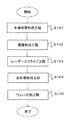
次に、第1実施形態に係る半導体発光素子の製造方法について説明する。図4は、第1実施形態に係る半導体発光素子の製造方法の流れを示すフローチャートである。
第1実施形態の半導体発光素子100の製造方法は、一例として、半導体層形成工程S101と、電極形成工程S102と、レーザースクライブ工程S103と、反射層形成工程S104と、ウェハ分割工程S105と、を含み、この順に行う。なお、各部材の材質や配置等については、前記した半導体発光素子100の説明で述べた通りであるので、ここでは適宜、説明を省略する。
<Method for Manufacturing Semiconductor Light Emitting Element>
Next, a method for manufacturing the semiconductor light emitting device according to the first embodiment will be described. FIG. 4 is a flowchart showing the flow of the method for manufacturing the semiconductor light emitting device according to the first embodiment.
The method for manufacturing the semiconductor
(半導体層形成工程、電極形成工程)
半導体層形成工程S101は、第1の主面と第1の主面に向かい合う第2の主面とを有する炭化物基板1の第1の主面上に半導体層20を形成する工程である。電極形成工程S102は、半導体層20上に電極、例えばp側全面電極5、p側パッド電極6を形成する工程である。半導体層20及び電極は、公知の製造方法によって形成され、一例として、以下の方法により形成することができる。
(Semiconductor layer forming process, electrode forming process)
The semiconductor layer forming step S101 is a step of forming the
半導体層20は、炭化物基板1の第1の主面上に、MOVPE反応装置にて、n型窒化物半導体層2、発光層3、p型窒化物半導体層4を構成するそれぞれの半導体を順次成長させる。
The
その後、ウェハの全面に、p側全面電極5として、例えばITO膜をスパッタリング装置にて成膜する。そして、p型窒化物半導体層4上のほぼ全面にITO膜が残るように、レジストマスクを形成してエッチングを行い、その後、レジストを除去する。次に、p側全面電極5上のそれぞれにおける所定領域を空けたマスクをフォトレジストにて形成する。そして、スパッタリング装置にて、ウェハ上に、パッド電極用の金属膜を連続的に順次成膜する。そして、レジストを除去し(リフトオフ)、p側パッド電極6を形成する。その後、p側パッド電極6が形成された側と異なる側のウェハを研削又は研磨し、凹凸を小さくする。
Thereafter, for example, an ITO film is formed as a p-side full-surface electrode 5 on the entire surface of the wafer by a sputtering apparatus. Then, a resist mask is formed and etched so that the ITO film remains on almost the entire surface of the p-type nitride semiconductor layer 4, and then the resist is removed. Next, a mask is formed with a photoresist in which a predetermined region on each of the p-side full-surface electrodes 5 is opened. Then, a metal film for the pad electrode is continuously and sequentially formed on the wafer by a sputtering apparatus. Then, the resist is removed (lift-off), and the p-
(レーザースクライブ工程)
レーザースクライブ工程S103は、レーザー照射によりウェハをチップ化する際の切断する部位(切断領域部)を作製する工程である。まず、チップ化する際のウェハを切断領域部において炭化物基板1の内部を焦点とするように、レーザー光を炭化物基板1側から照射する。これにより、基板1の内部に変質部を形成する。この変質部は基板1の厚み方向、つまり基板1の主面に対して略垂直な方向に延伸する割断溝である。レーザー光としては、例えばフェムト秒レーザーが挙げられる。
(Laser scribe process)
The laser scribing step S103 is a step of producing a portion (cutting region portion) to be cut when the wafer is chipped by laser irradiation. First, the laser beam is irradiated from the
(反射層形成工程)
反射層形成工程S104は、炭化物基板1の第2の主面側に、Agを主成分とし酸化物あるいは窒化物9を含有する反射層7を形成する工程である。
反射層7に酸化物を含有させる場合を例に説明する。なお、窒化物を含有させる場合は酸化物を窒化物に置き換えればよい。例えばAgターゲットと酸化物ターゲットとを用いた同時スパッタリング法、Ag及び酸化物を含む合金ターゲットを用いたスパッタリング法、又は、Ag及び酸化物を含む合金蒸着材料を用いた蒸着法により形成することができる。これらのスパッタリング法や蒸着法を用いることで、反射層7中に酸化物が分散された反射層7を形成することができる。
(Reflective layer forming process)
The reflective layer forming step S104 is a step of forming the
The case where an oxide is contained in the
合金ターゲットや合金蒸着材料に用いる合金は、Agを主成分とし、Ag中に酸化物9を含むことで合金としたものである。ここでは、酸化物9は、ナノサイズでAg中に分散させている。また、蒸着法としては、合金蒸着材料を用いる場合の他、Agからなる蒸着材料と、酸化物9からなる蒸着材料とを用いて、これらの蒸着材料を同時に蒸着させて反射層7を形成する方法を用いることもできる。スパッタリング法や蒸着法で使用するAgは純銀の場合も含む。
スパッタリング法や蒸着法のその他の条件や手順等は、公知の方法で行うことができる。
An alloy used for an alloy target or an alloy vapor deposition material is an alloy containing Ag as a main component and containing
Other conditions and procedures of the sputtering method and the vapor deposition method can be performed by known methods.
(ウェハ分割工程)
次に、切断領域部でウェハを切断し、個々の半導体発光素子をチップ状に分割する。ウェハ分割工程S105は、半導体層20、電極及び反射層7が形成されたウェハをチップに分割する工程である。
以上の工程を経て、半導体発光素子100を製造することができる。
(Wafer splitting process)
Next, the wafer is cut at the cutting region, and the individual semiconductor light emitting elements are divided into chips. The wafer dividing step S105 is a step of dividing the wafer on which the
The semiconductor
<第2実施形態>
つぎに、第2実施形態に係る半導体素子について説明する。第2実施形態に係る半導体素子は半導体発光素子である。図2Aは、第2実施形態に係る半導体発光素子の構成を模式的に示す底面図である。図2Bは、第2実施形態に係る半導体発光素子の構成を模式的に示す断面図であり、図2AのIIB−IIB‘線における断面を示す。図3A、図3Bは、第1、第2実施形態に係る半導体発光素子の炭化物基板と反射層との界面及び酸化物あるいは窒化物の状態を模式的に示す断面図である。
なお、第1実施形態と同様の構成を採るところについては、説明を省略することもある。
Second Embodiment
Next, a semiconductor element according to the second embodiment will be described. The semiconductor element according to the second embodiment is a semiconductor light emitting element. FIG. 2A is a bottom view schematically showing the configuration of the semiconductor light emitting device according to the second embodiment. 2B is a cross-sectional view schematically showing the configuration of the semiconductor light emitting device according to the second embodiment, and shows a cross section taken along the line IIB-IIB ′ of FIG. 2A. 3A and 3B are cross-sectional views schematically showing the interface between the carbide substrate and the reflective layer and the state of the oxide or nitride of the semiconductor light emitting device according to the first and second embodiments.
In addition, description may be abbreviate | omitted about the place which takes the structure similar to 1st Embodiment.
(半導体層及び電極)
半導体発光素子200は、炭化物基板101の第1の主面上に、接合層110を介して、p型窒化物半導体層104と、発光層103と、n型窒化物半導体層102とを積層して備える。更に、半導体発光素子200は、n型窒化物半導体層102上の一部の領域にn側パッド電極108を備える。また、炭化物基板101の第1の主面に向かい合う第2の主面上に、p側全面電極を兼ねる反射層107を備える。
(Semiconductor layer and electrode)
In the semiconductor
半導体層の材料としては、第1実施形態と同様に、例えば、InXAlYGa1−X−YN(0≦X、0≦Y、X+Y<1)等が好適に用いられる。n側パッド電極108の材料としては、例えば、Ag、Al、Ni、Rh、Ti、Pt、Pd、Mo、Cr、W、Cu、Au等の単体金属又はこれらの金属を主成分とする合金を用いることができる。或いは、前記の単体金属や、これらの金属を主成分とする合金を用いた積層構造とすることもできる。
As a material of the semiconductor layer, as in the first embodiment, for example, In X Al Y Ga 1- X-Y N (0 ≦ X, 0 ≦ Y, X + Y <1) or the like is preferably used. As a material of the n-
(炭化物基板)
炭化物基板101は、結晶成長用基板から分離した素子構造に接合させる接合用基板である。基板が導電性を有することで、上下電極(対向電極)構造を採用することができる。また、素子構造に面内均一に給電しやすく、電力効率を高めやすい。炭化物基板101としては、熱伝導性や導電性に優れたSiC基板などが挙げられる。
(Carbide substrate)
The
(接合層110)
接合層110は、上述の接合用基板である炭化物基板101と、結晶成長用基板から分離した半導体層120と、を接合させる層である。この接合層110は、金属反射膜又は誘電体多層膜を含んでいることが好ましい。これにより、半導体発光素子200では、素子構造から出射される光を接合層110の金属反射膜又は誘電体多層膜によって上方に効率良く反射させ、素子構造から出射される光が基板内部に進行することを抑制して、光の取り出し効率を高めることができる。なお、接合層110の金属反射膜又は誘電体多層膜は、素子構造に接して、又は、素子構造に接して設けられた導電性酸化物膜などの透光膜に接して、設けられることが、その光反射機能を発揮しやすいので好ましい。接合層に用いられる金属反射膜は、銀、アルミニウム、ロジウム、プラチナ、金、又はこれらの合金を用いることができ、なかでも光反射性に優れる銀又は銀合金が好ましい。接合層に用いられる誘電体多層膜は、例えばNb2O5とSiO2とのの積層構造など、シリコン、チタン、ジルコニウム、ニオブ、タンタル、アルミニウムのうちのいずれか一種の酸化物又は窒化物の少なくとも2つを繰り返し積層したものを用いることができる。金属反射膜は、接合層の一部又は全部に設けられ、誘電体多層膜は、接合層の一部に設けられる。金属反射膜や誘電体多層膜が接合層の一部に設けられる場合、接合層の他の部位は、金、錫、プラチナ、パラジウム、ロジウム、ニッケル、タングステン、モリブデン、クロム、チタン、又はこれらの合金やそれらの組み合わせにより構成することができる。なお、接合層は、接合用基板である基板と、結晶成長用基板から分離した素子構造と、を表面活性化接合や熱圧着などにより直接接合する場合には、省略することができる。
(Junction layer 110)
The
(反射層107)
反射層107は、第1実施形態と同様である。酸化物、窒化物から選択される少なくとも1種の粒子を含有する銀合金層であり、素子構造側への光の反射率を向上させて、光の取り出し効率を向上させる層である。また、p側全面電極としての機能を兼ねる。反射層107は、単層膜でも多層膜でもよい。反射層107は、スパッタ法、めっき法、蒸着法などにより形成することができる。反射層107に含有される酸化物あるいは窒化物109は、反射層107中に粒状の形態で分散されていたり、反射層107と炭化物基板101との界面に付着していたりする。
(Reflective layer 107)
The
以下、実施例について説明する。図5A〜図5Hは、それぞれ、実施例1〜6及び比較例1,2における成膜面に対してクロスカット法を施した後、成膜面側から撮影した写真である。 Examples will be described below. 5A to 5H are photographs taken from the film-forming surface side after the cross-cut method was performed on the film-forming surfaces in Examples 1 to 6 and Comparative Examples 1 and 2, respectively.
[実施例1]
密着性評価用サンプルを以下のようにして作製した。
まず、SiC単結晶基板C面上に、AgターゲットとSi3N4ターゲットを用いた同時スパッタリング法により、Si3N4を含有する反射層を120nmの厚さで成膜した。なお、同時スパッタリングのRFパワーはともに250Wとした。更にスパッタリング法により、反射層上に、第1金属層としてNi膜を100nmの厚さで、第2金属層としてRh膜を200nmの厚さで、第3金属層としてAu膜を500nmの厚さでこの順に成膜した。このようにして、SiC単結晶基板C面上に積層膜を形成した。
[Example 1]
A sample for evaluation of adhesion was prepared as follows.
First, a reflective layer containing Si 3 N 4 was formed to a thickness of 120 nm on the SiC single crystal substrate C surface by a co-sputtering method using an Ag target and a Si 3 N 4 target. The RF power for co-sputtering was 250 W for both. Further, by sputtering, a Ni film as the first metal layer has a thickness of 100 nm, a Rh film as the second metal layer has a thickness of 200 nm, and an Au film as the third metal layer has a thickness of 500 nm on the reflective layer. The films were formed in this order. In this way, a laminated film was formed on the SiC single crystal substrate C surface.
[実施例2]
実施例2の製造工程では、実施例1のSi3N4を含有する反射層の代わりに、ZnOを含有する反射層を形成した以外は、実施例1と同様にして、実施例2の半導体発光素子を製造した。なお、ZnOを含有する反射層はAgターゲットとZnOターゲットを用いた同時スパッタリング法により形成した。なお、同時スパッタリングのRFパワーはともに250Wとした。
[Example 2]
In the manufacturing process of Example 2, the semiconductor of Example 2 was made in the same manner as Example 1 except that a reflective layer containing ZnO was formed instead of the reflective layer containing Si 3 N 4 of Example 1. A light emitting device was manufactured. Note that the reflective layer containing ZnO was formed by a simultaneous sputtering method using an Ag target and a ZnO target. The RF power for co-sputtering was 250 W for both.
[実施例3]
実施例3の製造工程では、実施例1のSi3N4を含有する反射層の代わりに、TiO2を含有する反射層を形成した以外は、実施例1と同様にして、実施例3の半導体発光素子を製造した。なお、TiO2を含有する反射層はAgターゲットとTiO2ターゲットを用いた同時スパッタリング法により形成した。なお、同時スパッタリングのRFパワーはともに250Wとした。
[Example 3]
In the manufacturing process of Example 3, in the same manner as in Example 1 except that a reflective layer containing TiO 2 was formed instead of the reflective layer containing Si 3 N 4 of Example 1, Example 3 A semiconductor light emitting device was manufactured. The reflective layer containing TiO 2 was formed by a co-sputtering method using an Ag target and a TiO 2 target. The RF power for co-sputtering was 250 W for both.
[実施例4]
実施例4の製造工程では、実施例1のSi3N4を含有する反射層の代わりに、Ta2O5を含有する反射層を形成した以外は、実施例1と同様にして、実施例4の半導体発光素子を製造した。なお、Ta2O5を含有する反射層はAgターゲットとTa2O5ターゲットを用いた同時スパッタリング法により形成した。なお、同時スパッタリングのRFパワーはともに250Wとした。
[Example 4]
In the manufacturing process of Example 4, Example 1 was performed in the same manner as Example 1 except that a reflective layer containing Ta 2 O 5 was formed instead of the reflective layer containing Si 3 N 4 of Example 1. 4 semiconductor light emitting devices were manufactured. Note that the reflective layer containing Ta 2 O 5 was formed by a co-sputtering method using an Ag target and a Ta 2 O 5 target. The RF power for co-sputtering was 250 W for both.
[実施例5]
実施例5の製造工程では、実施例1のSi3N4を含有する反射層の代わりに、HfO2を含有する反射層を形成した以外は、実施例1と同様にして、実施例5の半導体発光素子を製造した。なお、HfO2を含有する反射層はAgターゲットとHfO2ターゲットを用いた同時スパッタリング法により形成した。なお、同時スパッタリングのRFパワーはともに250Wとした。
[Example 5]
In the manufacturing process of Example 5, in place of the reflective layer containing Si 3 N 4 of Example 1, a reflective layer containing HfO 2 was formed in the same manner as in Example 1 except that A semiconductor light emitting device was manufactured. Note that the reflective layer containing HfO 2 was formed by a co-sputtering method using an Ag target and an HfO 2 target. The RF power for co-sputtering was 250 W for both.
[実施例6]
実施例6の製造工程では、実施例1のSi3N4を含有する反射層の代わりに、In2O3を含有する反射層を形成した以外は、実施例1と同様にして、実施例6の半導体発光素子を製造した。なお、In2O3を含有する反射層はAgターゲットとIn2O3ターゲットを用いた同時スパッタリング法により形成した。なお、同時スパッタリングのRFパワーはともに250Wとした。
[Example 6]
In the manufacturing process of Example 6, Example 1 was performed in the same manner as Example 1 except that a reflective layer containing In 2 O 3 was formed instead of the reflective layer containing Si 3 N 4 of Example 1. 6 semiconductor light emitting devices were manufactured. Note that the reflective layer containing In 2 O 3 was formed by a simultaneous sputtering method using an Ag target and an In 2 O 3 target. The RF power for co-sputtering was 250 W for both.
[比較例1]
比較例1の製造工程では、実施例1のSi3N4を含有する反射層の代わりに、純銀層を形成した以外は、実施例1と同様にして、比較例1の半導体発光素子を製造した。なお、純銀層はAgターゲットのみを用いたスパッタリング法により形成した。なお、スパッタリングのRFパワーは500Wとした。
[Comparative Example 1]
In the manufacturing process of Comparative Example 1, the semiconductor light-emitting device of Comparative Example 1 was manufactured in the same manner as in Example 1 except that a pure silver layer was formed instead of the reflective layer containing Si 3 N 4 of Example 1. did. The pure silver layer was formed by a sputtering method using only an Ag target. The RF power for sputtering was 500W.
[比較例2]
比較例2の製造工程では、実施例1のSi3N4を含有する反射層の代わりに、TiCを含有する反射層を形成した以外は、実施例1と同様にして、比較例2の半導体発光素子を製造した。なお、TiCを含有する反射層はAgターゲットとTiCターゲットを用いた同時スパッタリング法により形成した。なお、同時スパッタリングのRFパワーはともに250Wとした。
[Comparative Example 2]
In the manufacturing process of Comparative Example 2, the semiconductor of Comparative Example 2 was prepared in the same manner as in Example 1 except that a reflective layer containing TiC was formed instead of the reflective layer containing Si 3 N 4 of Example 1. A light emitting device was manufactured. The reflective layer containing TiC was formed by a simultaneous sputtering method using an Ag target and a TiC target. The RF power for co-sputtering was 250 W for both.
上記実施例1、実施例2、実施例3、実施例4、実施例5、実施例6及び比較例1、比較例2のサンプルの成膜面に対して、クロスカット法(JIS K5600)を行った。テープ引き剥がし後の外観を成膜面側から観察した。観察は、キーエンス デジタルマイクロスコープVHX−700F装置を用い、25倍の条件で行った。
その結果、比較例1、比較例2ではSiC単結晶基板と反射層との界面で多く剥れていたのに対して、実施例1、実施例2、実施例3、実施例4、実施例5、実施例6では、それぞれSi3N4を含有する反射層、ZnOを含有する反射層、TiO2を含有する反射層、Ta2O5を含有する反射層、HfO2を含有する反射層、In2O3を含有する反射層の剥れが無かった。なお、図5G、Hの比較例1、2の写真において、図5A〜Fの実施例1〜6の写真と比較してクロスカット部以外の明度の異なる部位が、剥がれが生じた部位である。
A cross-cut method (JIS K5600) is applied to the film formation surfaces of the samples of Examples 1, 2, 3, 4, 5, and 6, and Comparative Examples 1 and 2. went. The appearance after peeling off the tape was observed from the film forming surface side. The observation was performed using a Keyence digital microscope VHX-700F apparatus under 25 times conditions.
As a result, the comparative example 1 and comparative example 2 were peeled off at the interface between the SiC single crystal substrate and the reflective layer, whereas the first example, the second example, the third example, the fourth example, and the second example. 5. In Example 6, a reflective layer containing Si 3 N 4 , a reflective layer containing ZnO, a reflective layer containing TiO 2 , a reflective layer containing Ta 2 O 5, and a reflective layer containing HfO 2 The reflective layer containing In 2 O 3 did not peel off. In addition, in the photograph of the comparative examples 1 and 2 of FIG. 5G and H, the site | part from which the brightness differs except a crosscut part compared with the photograph of Examples 1-6 of FIG. .
以上、本発明に係る半導体素子及びその製造方法について、発明を実施するための形態により具体的に説明したが、本発明の趣旨はこれらの記載に限定されるものではなく、特許請求の範囲の記載に基づいて広く解釈されなければならない。また、これらの記載に基づいて種々変更、改変等したものも本発明の趣旨に含まれることはいうまでもない。 The semiconductor element and the manufacturing method thereof according to the present invention have been specifically described above by the embodiments for carrying out the invention. However, the gist of the present invention is not limited to these descriptions, and the scope of the claims It must be interpreted widely based on the description. Needless to say, various changes and modifications based on these descriptions are also included in the spirit of the present invention.
本開示の実施形態に係る半導体素子は、各種照明器具、車両搭載用照明、ディスプレイ、インジケータ等の発光素子を用いる全ての半導体発光装置に利用することができる。また、受光装置等の光素子を用いた装置の他、パワートランジスタ等の半導体装置、半導体電子デバイスにも応用することができる。 The semiconductor element according to the embodiment of the present disclosure can be used for all semiconductor light-emitting devices using light-emitting elements such as various lighting fixtures, on-vehicle lighting, a display, and an indicator. Further, the present invention can be applied to a semiconductor device such as a power transistor and a semiconductor electronic device in addition to a device using an optical element such as a light receiving device.
1、101 炭化物基板
2、102 n型窒化物半導体層
3、103 発光層
4、104 p型窒化物半導体層
5 p側全面電極
6 p側パッド電極
7、107 反射層
108 n側パッド電極
9、109 酸化物あるいは窒化物
110 接合層
20、120 半導体層
100、200 半導体発光素子(半導体素子)
B 擬似的な遷移層
DESCRIPTION OF SYMBOLS 1,101 Carbide substrate 2,102 N-type nitride semiconductor layer 3,103 Light emitting layer 4,104 P-type nitride semiconductor layer 5P side whole surface electrode 6P side pad electrode 7,107 Reflective layer 108 N
B Pseudo transition layer
Claims (17)
炭化物基板と、
酸化物、窒化物から選択される少なくとも1種の粒子を含有するAgを主成分とする反射層と、がこの順に配置された半導体素子。 A semiconductor layer;
A carbide substrate;
A semiconductor element in which a reflective layer mainly composed of Ag containing at least one kind of particles selected from oxides and nitrides is arranged in this order.
前記炭化物基板における前記半導体層が設けられた面と反対側の面に、酸化物、窒化物から選択される少なくとも1種の粒子を含有するAgを主成分とする反射層を形成する工程と、を含む半導体素子の製造方法。 Forming a semiconductor layer on the carbide substrate;
Forming a reflective layer mainly composed of Ag containing at least one kind of particles selected from oxides and nitrides on the surface of the carbide substrate opposite to the surface on which the semiconductor layer is provided; A method for manufacturing a semiconductor device comprising:
Priority Applications (3)
| Application Number | Priority Date | Filing Date | Title |
|---|---|---|---|
| JP2016234596A JP6834424B2 (en) | 2016-12-02 | 2016-12-02 | Semiconductor devices and their manufacturing methods |
| US15/825,106 US10615312B2 (en) | 2016-12-02 | 2017-11-29 | Semiconductor element and method for manufacturing the same |
| US16/803,893 US10868219B2 (en) | 2016-12-02 | 2020-02-27 | Method for manufacturing semiconductor element |
Applications Claiming Priority (1)
| Application Number | Priority Date | Filing Date | Title |
|---|---|---|---|
| JP2016234596A JP6834424B2 (en) | 2016-12-02 | 2016-12-02 | Semiconductor devices and their manufacturing methods |
Publications (2)
| Publication Number | Publication Date |
|---|---|
| JP2018093035A true JP2018093035A (en) | 2018-06-14 |
| JP6834424B2 JP6834424B2 (en) | 2021-02-24 |
Family
ID=62244114
Family Applications (1)
| Application Number | Title | Priority Date | Filing Date |
|---|---|---|---|
| JP2016234596A Active JP6834424B2 (en) | 2016-12-02 | 2016-12-02 | Semiconductor devices and their manufacturing methods |
Country Status (2)
| Country | Link |
|---|---|
| US (2) | US10615312B2 (en) |
| JP (1) | JP6834424B2 (en) |
Families Citing this family (1)
| Publication number | Priority date | Publication date | Assignee | Title |
|---|---|---|---|---|
| US11476399B2 (en) * | 2017-11-29 | 2022-10-18 | Panasonic Intellectual Property Management Co., Ltd. | Jointing material, fabrication method for semiconductor device using the jointing material, and semiconductor device |
Citations (6)
| Publication number | Priority date | Publication date | Assignee | Title |
|---|---|---|---|---|
| JP2008514028A (en) * | 2004-09-22 | 2008-05-01 | クリー インコーポレイテッド | High efficiency III-nitride LED with lenticular surface |
| JP2010263050A (en) * | 2009-05-01 | 2010-11-18 | Showa Denko Kk | LIGHT EMITTING DIODE, MANUFACTURING METHOD THEREOF, AND LIGHT EMITTING DIODE LAMP |
| JP2013021252A (en) * | 2011-07-14 | 2013-01-31 | Toshiba Corp | Semiconductor light-emitting element |
| US20150060880A1 (en) * | 2012-06-21 | 2015-03-05 | Xiamen Sanan Optoelectronics Technology Co., Ltd. | GaN-Based LED |
| JP2015106642A (en) * | 2013-11-29 | 2015-06-08 | 日亜化学工業株式会社 | Reflection coating for light-emitting board, lead frame including the same, wiring board, wire, and light-emitting board |
| JP2015144245A (en) * | 2013-12-25 | 2015-08-06 | 日亜化学工業株式会社 | Semiconductor element, semiconductor device including the same, and method for manufacturing semiconductor element |
Family Cites Families (8)
| Publication number | Priority date | Publication date | Assignee | Title |
|---|---|---|---|---|
| JP2005072148A (en) | 2003-08-21 | 2005-03-17 | Mitsubishi Cable Ind Ltd | Nitride semiconductor devices |
| JP2009245981A (en) * | 2008-03-28 | 2009-10-22 | Toyota Central R&D Labs Inc | Led light-emitting device |
| BR112014028110A2 (en) * | 2012-05-09 | 2017-06-27 | Amedica Corp | methods for changing the surface chemistry of biomedical implants and related equipment |
| US9121100B2 (en) * | 2012-12-14 | 2015-09-01 | Intermolecular, Inc. | Silver based conductive layer for flexible electronics |
| JP2014179063A (en) * | 2013-02-13 | 2014-09-25 | Panasonic Corp | Touch panel |
| JP6197696B2 (en) | 2014-02-28 | 2017-09-20 | 日亜化学工業株式会社 | LIGHT EMITTING DEVICE MANUFACTURING METHOD AND LIGHT EMITTING DEVICE |
| JP6398541B2 (en) | 2014-09-29 | 2018-10-03 | 日亜化学工業株式会社 | Lead frame and light emitting device |
| JP6409457B2 (en) | 2014-09-29 | 2018-10-24 | 日亜化学工業株式会社 | Semiconductor light emitting element and light emitting device |
-
2016
- 2016-12-02 JP JP2016234596A patent/JP6834424B2/en active Active
-
2017
- 2017-11-29 US US15/825,106 patent/US10615312B2/en active Active
-
2020
- 2020-02-27 US US16/803,893 patent/US10868219B2/en active Active
Patent Citations (6)
| Publication number | Priority date | Publication date | Assignee | Title |
|---|---|---|---|---|
| JP2008514028A (en) * | 2004-09-22 | 2008-05-01 | クリー インコーポレイテッド | High efficiency III-nitride LED with lenticular surface |
| JP2010263050A (en) * | 2009-05-01 | 2010-11-18 | Showa Denko Kk | LIGHT EMITTING DIODE, MANUFACTURING METHOD THEREOF, AND LIGHT EMITTING DIODE LAMP |
| JP2013021252A (en) * | 2011-07-14 | 2013-01-31 | Toshiba Corp | Semiconductor light-emitting element |
| US20150060880A1 (en) * | 2012-06-21 | 2015-03-05 | Xiamen Sanan Optoelectronics Technology Co., Ltd. | GaN-Based LED |
| JP2015106642A (en) * | 2013-11-29 | 2015-06-08 | 日亜化学工業株式会社 | Reflection coating for light-emitting board, lead frame including the same, wiring board, wire, and light-emitting board |
| JP2015144245A (en) * | 2013-12-25 | 2015-08-06 | 日亜化学工業株式会社 | Semiconductor element, semiconductor device including the same, and method for manufacturing semiconductor element |
Non-Patent Citations (1)
| Title |
|---|
| M. SHATALOV ET AL.: ""Deep ultraviolet light-emitting diodes using quaternary AlInGaN multiple quantum wells"", IEEE JOURNAL ON SELECTED TOPICS IN QUANTUM ELECTRONICS, vol. 8, no. 2, JPN6020021987, March 2002 (2002-03-01), ISSN: 0004292167 * |
Also Published As
| Publication number | Publication date |
|---|---|
| US10868219B2 (en) | 2020-12-15 |
| US20200203575A1 (en) | 2020-06-25 |
| JP6834424B2 (en) | 2021-02-24 |
| US10615312B2 (en) | 2020-04-07 |
| US20180158991A1 (en) | 2018-06-07 |
Similar Documents
| Publication | Publication Date | Title |
|---|---|---|
| US6960485B2 (en) | Light-emitting device using a group III nitride compound semiconductor and a method of manufacture | |
| KR101064020B1 (en) | Light emitting device and manufacturing method | |
| JP4946195B2 (en) | Semiconductor light emitting device and manufacturing method thereof | |
| JP4557542B2 (en) | Nitride light emitting device and high luminous efficiency nitride light emitting device | |
| JP5073917B2 (en) | Optoelectronic semiconductor chip having electrical contacts and method for manufacturing the optoelectronic semiconductor chip | |
| JP2008537318A (en) | Light emitting diode with conductive metal substrate | |
| JP5258853B2 (en) | Semiconductor light emitting device and manufacturing method thereof | |
| JP2011505699A (en) | Gallium nitride thin LED with enhanced light output | |
| CN100550447C (en) | Flip chip type nitride semiconductor light emitting device | |
| JP2003086843A (en) | Semiconductor light emitting element and semiconductor light emitting device | |
| JP2009295611A (en) | Semiconductor light emitting element and manufacturing method thereof | |
| JP5030398B2 (en) | Gallium nitride compound semiconductor light emitting device | |
| WO2011077748A1 (en) | Vertical group iii nitride semiconductor light-emitting element and production method therefor | |
| JP6040769B2 (en) | Light emitting device and manufacturing method thereof | |
| JP2010272592A (en) | Semiconductor light emitting device | |
| US7352009B2 (en) | Light emitting nitride semiconductor device and method of fabricating the same | |
| US10868219B2 (en) | Method for manufacturing semiconductor element | |
| JP6119906B2 (en) | Light emitting element | |
| JP2008192825A (en) | Semiconductor light-emitting element | |
| JP6806446B2 (en) | Semiconductor devices and their manufacturing methods | |
| JP2009094108A (en) | Manufacturing method of GaN-based LED element | |
| US9093356B2 (en) | Semiconductor light emitting element | |
| JP5974808B2 (en) | Semiconductor light emitting device | |
| JP4241057B2 (en) | Oxide semiconductor light emitting device and manufacturing method thereof | |
| KR20050023540A (en) | Light Emitting Devices |
Legal Events
| Date | Code | Title | Description |
|---|---|---|---|
| A621 | Written request for application examination |
Free format text: JAPANESE INTERMEDIATE CODE: A621 Effective date: 20190625 |
|
| A977 | Report on retrieval |
Free format text: JAPANESE INTERMEDIATE CODE: A971007 Effective date: 20200520 |
|
| A131 | Notification of reasons for refusal |
Free format text: JAPANESE INTERMEDIATE CODE: A131 Effective date: 20200630 |
|
| A521 | Request for written amendment filed |
Free format text: JAPANESE INTERMEDIATE CODE: A523 Effective date: 20200820 |
|
| TRDD | Decision of grant or rejection written | ||
| A01 | Written decision to grant a patent or to grant a registration (utility model) |
Free format text: JAPANESE INTERMEDIATE CODE: A01 Effective date: 20210105 |
|
| A61 | First payment of annual fees (during grant procedure) |
Free format text: JAPANESE INTERMEDIATE CODE: A61 Effective date: 20210118 |
|
| R150 | Certificate of patent or registration of utility model |
Ref document number: 6834424 Country of ref document: JP Free format text: JAPANESE INTERMEDIATE CODE: R150 |
|
| R250 | Receipt of annual fees |
Free format text: JAPANESE INTERMEDIATE CODE: R250 |
|
| R250 | Receipt of annual fees |
Free format text: JAPANESE INTERMEDIATE CODE: R250 |
|
| R250 | Receipt of annual fees |
Free format text: JAPANESE INTERMEDIATE CODE: R250 |