JP2018029128A - Dopant introduction method - Google Patents
Dopant introduction method Download PDFInfo
- Publication number
- JP2018029128A JP2018029128A JP2016160377A JP2016160377A JP2018029128A JP 2018029128 A JP2018029128 A JP 2018029128A JP 2016160377 A JP2016160377 A JP 2016160377A JP 2016160377 A JP2016160377 A JP 2016160377A JP 2018029128 A JP2018029128 A JP 2018029128A
- Authority
- JP
- Japan
- Prior art keywords
- dopant
- semiconductor wafer
- germanium
- flash
- chamber
- Prior art date
- Legal status (The legal status is an assumption and is not a legal conclusion. Google has not performed a legal analysis and makes no representation as to the accuracy of the status listed.)
- Pending
Links
Images


Landscapes
- Container, Conveyance, Adherence, Positioning, Of Wafer (AREA)
Abstract
Description
本発明は、半導体基板にドーパントを注入して活性化させるドーパント導入方法に関する。 The present invention relates to a dopant introduction method in which a dopant is implanted into a semiconductor substrate and activated.
半導体デバイスの製造プロセスにおいて、単結晶のシリコン(Si)またはゲルマニウム(Ge)へのドーパントの導入は必要不可欠な工程である。ドーパントを導入することによって、n型半導体またはp型半導体が作成される。ドーパントの導入は、典型的にはゲルマニウム等の半導体基板にボロン(B)、ヒ素(As)、リン(P)等のドーパント原子をイオン注入し、その半導体基板にアニール処理を施してドーパント原子を活性化させることによって実現される(例えば、特許文献1)。 In a semiconductor device manufacturing process, introduction of a dopant into single crystal silicon (Si) or germanium (Ge) is an indispensable step. By introducing a dopant, an n-type semiconductor or a p-type semiconductor is produced. Typically, dopant is introduced by ion-implanting dopant atoms such as boron (B), arsenic (As), and phosphorus (P) into a semiconductor substrate such as germanium, and subjecting the semiconductor substrate to an annealing treatment to introduce the dopant atoms. This is realized by activation (for example, Patent Document 1).
ドーパント原子を活性化させるためのアニール処理では同時に原子の拡散も生じるのであるが、近年の半導体デバイスに要求されている浅い接合を実現するためにはドーパント原子が長距離を拡散することは望ましくない。このため、特許文献1に開示されるようなフラッシュランプアニールによって極めて短い時間で活性化のための加熱処理を行うことが試みられている。また、加熱処理時の温度が低いほどドーパント原子の拡散を抑制することができるのであるが、活性化率も低くなるという問題が生じる。そこで、アニール処理時の処理温度が低くても高い活性化率を得ることができる技術が求められている。また、単に高い活性化率を得るだけでなく、適正な値に活性化率を制御することへの要望も強い。
Annealing treatment for activating dopant atoms also causes diffusion of atoms at the same time, but it is not desirable for dopant atoms to diffuse long distances in order to realize the shallow junction required in recent semiconductor devices. . For this reason, it has been attempted to perform heat treatment for activation in a very short time by flash lamp annealing as disclosed in
本発明は、上記課題に鑑みてなされたものであり、ドーパントの活性化率を適正に制御することができるドーパント導入方法を提供することを目的とする。 This invention is made | formed in view of the said subject, and it aims at providing the dopant introduction | transduction method which can control the activation rate of a dopant appropriately.
上記課題を解決するため、請求項1の発明は、半導体基板にドーパントを注入して活性化させるドーパント導入方法において、半導体基板の表面にイオン注入を行って当該表面の結晶中に空孔を形成する空孔形成工程と、前記半導体基板の表面にドーパントを注入するドーパント注入工程と、前記半導体基板の表面を加熱して前記ドーパントを活性化させるアニール工程と、を備えることを特徴とする。
In order to solve the above problems, the invention of
また、請求項2の発明は、請求項1の発明に係るドーパント導入方法において、前記空孔形成工程でのイオン注入のドーズ量は、前記ドーパント注入工程にて前記ドーパントが注入される前記半導体基板の表面からの深さ位置がアモルファス化されるドーズ量未満とすることを特徴とする。
The invention of
また、請求項3の発明は、請求項1または請求項2の発明に係るドーパント導入方法において、前記空孔形成工程でのイオン注入にて前記ドーパントを前記半導体基板の表面に注入して前記空孔形成工程と前記ドーパント注入工程とを並行して行うことを特徴とする。 According to a third aspect of the present invention, in the dopant introduction method according to the first or second aspect of the present invention, the dopant is implanted into the surface of the semiconductor substrate by ion implantation in the vacancy formation step, and the vacancy is introduced. The hole forming step and the dopant implantation step are performed in parallel.
また、請求項4の発明は、請求項1から請求項3のいずれかの発明に係るドーパント導入方法において、前記半導体基板は、ゲルマニウム、シリコンゲルマニウムまたはシリコンにて形成されることを特徴とする。 According to a fourth aspect of the present invention, in the dopant introduction method according to any one of the first to third aspects, the semiconductor substrate is formed of germanium, silicon germanium, or silicon.
また、請求項5の発明は、請求項1から請求項4のいずれかの発明に係るドーパント導入方法において、前記アニール工程では、前記半導体基板の表面にフラッシュランプからフラッシュ光を照射して当該表面を加熱することを特徴とする。
Further, the invention of
請求項1から請求項5の発明によれば、半導体基板の表面にイオン注入を行って当該表面の結晶中に空孔を形成するとともに、半導体基板の表面にドーパントを注入し、その半導体基板の表面を加熱してドーパントを活性化させるため、打ち込まれたドーパントが空孔に入り込んで活性化され、高い活性化率を得ることができる。また、空孔形成工程でのイオン注入時のドーズ量を調整することによって、ドーパントの活性化率を適正な値に制御することができる。 According to the first to fifth aspects of the present invention, ions are implanted into the surface of the semiconductor substrate to form vacancies in the crystal of the surface, and a dopant is implanted into the surface of the semiconductor substrate. Since the surface is heated to activate the dopant, the implanted dopant enters the vacancies and is activated, and a high activation rate can be obtained. Further, the dopant activation rate can be controlled to an appropriate value by adjusting the dose during ion implantation in the vacancy formation step.
特に、請求項3の発明によれば、空孔形成工程でのイオン注入にてドーパントを半導体基板の表面に注入して空孔形成工程とドーパント注入工程とを並行して行うため、イオン注入を1回で完了させることができ、処理時間を短縮することができる。 In particular, according to the invention of claim 3, since the dopant is implanted into the surface of the semiconductor substrate by the ion implantation in the vacancy formation step and the vacancy formation step and the dopant implantation step are performed in parallel, the ion implantation is performed. It can be completed at once, and the processing time can be shortened.
以下、図面を参照しつつ本発明の実施の形態について詳細に説明する。 Hereinafter, embodiments of the present invention will be described in detail with reference to the drawings.
まず、本発明に係るドーパント導入方法を実施する際に必要となる熱処理を実行する熱処理装置について説明する。図1は、本発明に係るドーパント導入方法に使用する熱処理装置1の構成を示す縦断面図である。図1の熱処理装置1は、基板として円板形状の半導体ウェハーWに対してフラッシュ光照射を行うことによってその半導体ウェハーWを加熱するフラッシュランプアニール装置である。処理対象となる半導体ウェハーWのサイズは特に限定されるものではないが、例えばφ300mmやφ450mmである。なお、図1および以降の各図においては、理解容易のため、必要に応じて各部の寸法や数を誇張または簡略化して描いている。
First, the heat processing apparatus which performs the heat processing required when implementing the dopant introduction | transduction method concerning this invention is demonstrated. FIG. 1 is a longitudinal sectional view showing a configuration of a
熱処理装置1は、半導体ウェハーWを収容するチャンバー6と、複数のフラッシュランプFLを内蔵するフラッシュ加熱部5と、複数のハロゲンランプHLを内蔵するハロゲン加熱部4と、を備える。チャンバー6の上側にフラッシュ加熱部5が設けられるとともに、下側にハロゲン加熱部4が設けられている。また、熱処理装置1は、チャンバー6の内部に、半導体ウェハーWを水平姿勢に保持する保持部7と、保持部7と装置外部との間で半導体ウェハーWの受け渡しを行う移載機構10と、を備える。さらに、熱処理装置1は、ハロゲン加熱部4、フラッシュ加熱部5およびチャンバー6に設けられた各動作機構を制御して半導体ウェハーWの熱処理を実行させる制御部3を備える。
The
チャンバー6は、筒状のチャンバー側部61の上下に石英製のチャンバー窓を装着して構成されている。チャンバー側部61は上下が開口された概略筒形状を有しており、上側開口には上側チャンバー窓63が装着されて閉塞され、下側開口には下側チャンバー窓64が装着されて閉塞されている。チャンバー6の天井部を構成する上側チャンバー窓63は、石英により形成された円板形状部材であり、フラッシュ加熱部5から出射されたフラッシュ光をチャンバー6内に透過する石英窓として機能する。また、チャンバー6の床部を構成する下側チャンバー窓64も、石英により形成された円板形状部材であり、ハロゲン加熱部4からの光をチャンバー6内に透過する石英窓として機能する。
The
また、チャンバー側部61の内側の壁面の上部には反射リング68が装着され、下部には反射リング69が装着されている。反射リング68,69は、ともに円環状に形成されている。上側の反射リング68は、チャンバー側部61の上側から嵌め込むことによって装着される。一方、下側の反射リング69は、チャンバー側部61の下側から嵌め込んで図示省略のビスで留めることによって装着される。すなわち、反射リング68,69は、ともに着脱自在にチャンバー側部61に装着されるものである。チャンバー6の内側空間、すなわち上側チャンバー窓63、下側チャンバー窓64、チャンバー側部61および反射リング68,69によって囲まれる空間が熱処理空間65として規定される。
A
チャンバー側部61に反射リング68,69が装着されることによって、チャンバー6の内壁面に凹部62が形成される。すなわち、チャンバー側部61の内壁面のうち反射リング68,69が装着されていない中央部分と、反射リング68の下端面と、反射リング69の上端面とで囲まれた凹部62が形成される。凹部62は、チャンバー6の内壁面に水平方向に沿って円環状に形成され、半導体ウェハーWを保持する保持部7を囲繞する。チャンバー側部61および反射リング68,69は、強度と耐熱性に優れた金属材料(例えば、ステンレススチール)にて形成されている。
By attaching the
また、チャンバー側部61には、チャンバー6に対して半導体ウェハーWの搬入および搬出を行うための搬送開口部(炉口)66が形設されている。搬送開口部66は、ゲートバルブ185によって開閉可能とされている。搬送開口部66は凹部62の外周面に連通接続されている。このため、ゲートバルブ185が搬送開口部66を開放しているときには、搬送開口部66から凹部62を通過して熱処理空間65への半導体ウェハーWの搬入および熱処理空間65からの半導体ウェハーWの搬出を行うことができる。また、ゲートバルブ185が搬送開口部66を閉鎖するとチャンバー6内の熱処理空間65が密閉空間とされる。
The
また、チャンバー6の内壁上部には熱処理空間65に処理ガスを供給するガス供給孔81が形設されている。ガス供給孔81は、凹部62よりも上側位置に形設されており、反射リング68に設けられていても良い。ガス供給孔81はチャンバー6の側壁内部に円環状に形成された緩衝空間82を介してガス供給管83に連通接続されている。ガス供給管83は処理ガス供給源85に接続されている。また、ガス供給管83の経路途中にはバルブ84が介挿されている。バルブ84が開放されると、処理ガス供給源85から緩衝空間82に処理ガスが送給される。緩衝空間82に流入した処理ガスは、ガス供給孔81よりも流体抵抗の小さい緩衝空間82内を拡がるように流れてガス供給孔81から熱処理空間65内へと供給される。処理ガスとしては、窒素(N2)等の不活性ガス、または、水素(H2)、アンモニア(NH3)等の反応性ガスを用いることができる(本実施形態では窒素)。
A
一方、チャンバー6の内壁下部には熱処理空間65内の気体を排気するガス排気孔86が形設されている。ガス排気孔86は、凹部62よりも下側位置に形設されており、反射リング69に設けられていても良い。ガス排気孔86はチャンバー6の側壁内部に円環状に形成された緩衝空間87を介してガス排気管88に連通接続されている。ガス排気管88は排気部190に接続されている。また、ガス排気管88の経路途中にはバルブ89が介挿されている。バルブ89が開放されると、熱処理空間65の気体がガス排気孔86から緩衝空間87を経てガス排気管88へと排出される。なお、ガス供給孔81およびガス排気孔86は、チャンバー6の周方向に沿って複数設けられていても良いし、スリット状のものであっても良い。また、処理ガス供給源85および排気部190は、熱処理装置1に設けられた機構であっても良いし、熱処理装置1が設置される工場のユーティリティであっても良い。
On the other hand, a
また、搬送開口部66の先端にも熱処理空間65内の気体を排出するガス排気管191が接続されている。ガス排気管191はバルブ192を介して排気部190に接続されている。バルブ192を開放することによって、搬送開口部66を介してチャンバー6内の気体が排気される。
A
図2は、保持部7の全体外観を示す斜視図である。保持部7は、基台リング71、連結部72およびサセプタ74を備えて構成される。基台リング71、連結部72およびサセプタ74はいずれも石英にて形成されている。すなわち、保持部7の全体が石英にて形成されている。
FIG. 2 is a perspective view showing the overall appearance of the holding unit 7. The holding part 7 includes a
基台リング71は円環形状から一部が欠落した円弧形状の石英部材である。この欠落部分は、後述する移載機構10の移載アーム11と基台リング71との干渉を防ぐために設けられている。基台リング71は凹部62の底面に載置されることによって、チャンバー6の壁面に支持されることとなる(図1参照)。基台リング71の上面に、その円環形状の周方向に沿って複数の連結部72(本実施形態では4個)が立設される。連結部72も石英の部材であり、溶接によって基台リング71に固着される。
The
サセプタ74は基台リング71に設けられた4個の連結部72によって支持される。図3は、サセプタ74の平面図である。また、図4は、サセプタ74の断面図である。サセプタ74は、保持プレート75、ガイドリング76および複数の基板支持ピン77を備える。保持プレート75は、石英にて形成された略円形の平板状部材である。保持プレート75の直径は半導体ウェハーWの直径よりも大きい。すなわち、保持プレート75は、半導体ウェハーWよりも大きな平面サイズを有する。
The
保持プレート75の上面周縁部にガイドリング76が設置されている。ガイドリング76は、半導体ウェハーWの直径よりも大きな内径を有する円環形状の部材である。例えば、半導体ウェハーWの直径がφ300mmの場合、ガイドリング76の内径はφ320mmである。ガイドリング76の内周は、保持プレート75から上方に向けて広くなるようなテーパ面とされている。ガイドリング76は、保持プレート75と同様の石英にて形成される。ガイドリング76は、保持プレート75の上面に溶着するようにしても良いし、別途加工したピンなどによって保持プレート75に固定するようにしても良い。或いは、保持プレート75とガイドリング76とを一体の部材として加工するようにしても良い。
A
保持プレート75の上面のうちガイドリング76よりも内側の領域が半導体ウェハーWを保持する平面状の保持面75aとされる。保持プレート75の保持面75aには、複数の基板支持ピン77が立設されている。本実施形態においては、保持面75aの外周円(ガイドリング76の内周円)と同心円の周上に沿って30°毎に計12個の基板支持ピン77が立設されている。12個の基板支持ピン77を配置した円の径(対向する基板支持ピン77間の距離)は半導体ウェハーWの径よりも小さく、半導体ウェハーWの径がφ300mmであればφ270mm〜φ280mm(本実施形態ではφ280mm)である。それぞれの基板支持ピン77は石英にて形成されている。複数の基板支持ピン77は、保持プレート75の上面に溶接によって設けるようにしても良いし、保持プレート75と一体に加工するようにしても良い。
A region inside the
図2に戻り、基台リング71に立設された4個の連結部72とサセプタ74の保持プレート75の周縁部とが溶接によって固着される。すなわち、サセプタ74と基台リング71とは連結部72によって固定的に連結されている。このような保持部7の基台リング71がチャンバー6の壁面に支持されることによって、保持部7がチャンバー6に装着される。保持部7がチャンバー6に装着された状態においては、サセプタ74の保持プレート75は水平姿勢(法線が鉛直方向と一致する姿勢)となる。すなわち、保持プレート75の保持面75aは水平面となる。
Returning to FIG. 2, the four connecting
チャンバー6に搬入された半導体ウェハーWは、チャンバー6に装着された保持部7のサセプタ74の上に水平姿勢にて載置されて保持される。このとき、半導体ウェハーWは保持プレート75上に立設された12個の基板支持ピン77によって支持されてサセプタ74に保持される。より厳密には、12個の基板支持ピン77の上端部が半導体ウェハーWの下面に接触して当該半導体ウェハーWを支持する。12個の基板支持ピン77の高さ(基板支持ピン77の上端から保持プレート75の保持面75aまでの距離)は均一であるため、12個の基板支持ピン77によって半導体ウェハーWを水平姿勢に支持することができる。
The semiconductor wafer W carried into the
また、半導体ウェハーWは複数の基板支持ピン77によって保持プレート75の保持面75aから所定の間隔を隔てて支持されることとなる。基板支持ピン77の高さよりもガイドリング76の厚さの方が大きい。従って、複数の基板支持ピン77によって支持された半導体ウェハーWの水平方向の位置ずれはガイドリング76によって防止される。
Further, the semiconductor wafer W is supported by a plurality of substrate support pins 77 at a predetermined interval from the holding
また、図2および図3に示すように、サセプタ74の保持プレート75には、上下に貫通して開口部78が形成されている。開口部78は、放射温度計120(図1参照)がサセプタ74に保持された半導体ウェハーWの下面から放射される放射光(赤外光)を受光するために設けられている。すなわち、放射温度計120が開口部78を介してサセプタ74に保持された半導体ウェハーWの下面から放射された光を受光し、別置のディテクタによってその半導体ウェハーWの温度が測定される。さらに、サセプタ74の保持プレート75には、後述する移載機構10のリフトピン12が半導体ウェハーWの受け渡しのために貫通する4個の貫通孔79が穿設されている。
As shown in FIGS. 2 and 3, the holding
図5は、移載機構10の平面図である。また、図6は、移載機構10の側面図である。移載機構10は、2本の移載アーム11を備える。移載アーム11は、概ね円環状の凹部62に沿うような円弧形状とされている。それぞれの移載アーム11には2本のリフトピン12が立設されている。各移載アーム11は水平移動機構13によって回動可能とされている。水平移動機構13は、一対の移載アーム11を保持部7に対して半導体ウェハーWの移載を行う移載動作位置(図5の実線位置)と保持部7に保持された半導体ウェハーWと平面視で重ならない退避位置(図5の二点鎖線位置)との間で水平移動させる。水平移動機構13としては、個別のモータによって各移載アーム11をそれぞれ回動させるものであっても良いし、リンク機構を用いて1個のモータによって一対の移載アーム11を連動させて回動させるものであっても良い。
FIG. 5 is a plan view of the
また、一対の移載アーム11は、昇降機構14によって水平移動機構13とともに昇降移動される。昇降機構14が一対の移載アーム11を移載動作位置にて上昇させると、計4本のリフトピン12がサセプタ74に穿設された貫通孔79(図2,3参照)を通過し、リフトピン12の上端がサセプタ74の上面から突き出る。一方、昇降機構14が一対の移載アーム11を移載動作位置にて下降させてリフトピン12を貫通孔79から抜き取り、水平移動機構13が一対の移載アーム11を開くように移動させると各移載アーム11が退避位置に移動する。一対の移載アーム11の退避位置は、保持部7の基台リング71の直上である。基台リング71は凹部62の底面に載置されているため、移載アーム11の退避位置は凹部62の内側となる。なお、移載機構10の駆動部(水平移動機構13および昇降機構14)が設けられている部位の近傍にも図示省略の排気機構が設けられており、移載機構10の駆動部周辺の雰囲気がチャンバー6の外部に排出されるように構成されている。
The pair of
図1に戻り、チャンバー6の上方に設けられたフラッシュ加熱部5は、筐体51の内側に、複数本(本実施形態では30本)のキセノンフラッシュランプFLからなる光源と、その光源の上方を覆うように設けられたリフレクタ52と、を備えて構成される。また、フラッシュ加熱部5の筐体51の底部にはランプ光放射窓53が装着されている。フラッシュ加熱部5の床部を構成するランプ光放射窓53は、石英により形成された板状の石英窓である。フラッシュ加熱部5がチャンバー6の上方に設置されることにより、ランプ光放射窓53が上側チャンバー窓63と相対向することとなる。フラッシュランプFLはチャンバー6の上方からランプ光放射窓53および上側チャンバー窓63を介して熱処理空間65にフラッシュ光を照射する。
Returning to FIG. 1, the
複数のフラッシュランプFLは、それぞれが長尺の円筒形状を有する棒状ランプであり、それぞれの長手方向が保持部7に保持される半導体ウェハーWの主面に沿って(つまり水平方向に沿って)互いに平行となるように平面状に配列されている。よって、フラッシュランプFLの配列によって形成される平面も水平面である。 Each of the plurality of flash lamps FL is a rod-shaped lamp having a long cylindrical shape, and the longitudinal direction of each of the flash lamps FL is along the main surface of the semiconductor wafer W held by the holding unit 7 (that is, along the horizontal direction). They are arranged in a plane so as to be parallel to each other. Therefore, the plane formed by the arrangement of the flash lamps FL is also a horizontal plane.
図8は、フラッシュランプFLの駆動回路を示す図である。同図に示すように、コンデンサ93と、コイル94と、フラッシュランプFLと、IGBT(絶縁ゲートバイポーラトランジスタ)96とが直列に接続されている。また、図8に示すように、制御部3は、パルス発生器31および波形設定部32を備えるとともに、入力部33に接続されている。入力部33としては、キーボード、マウス、タッチパネル等の種々の公知の入力機器を採用することができる。入力部33からの入力内容に基づいて波形設定部32がパルス信号の波形を設定し、その波形に従ってパルス発生器31がパルス信号を発生する。
FIG. 8 is a diagram showing a driving circuit for the flash lamp FL. As shown in the figure, a
フラッシュランプFLは、その内部にキセノンガスが封入されその両端部に陽極および陰極が配設された棒状のガラス管(放電管)92と、該ガラス管92の外周面上に付設されたトリガー電極91とを備える。コンデンサ93には、電源ユニット95によって所定の電圧が印加され、その印加電圧(充電電圧)に応じた電荷が充電される。また、トリガー電極91にはトリガー回路97から高電圧を印加することができる。トリガー回路97がトリガー電極91に電圧を印加するタイミングは制御部3によって制御される。
The flash lamp FL includes a rod-shaped glass tube (discharge tube) 92 in which xenon gas is sealed and an anode and a cathode are disposed at both ends thereof, and a trigger electrode provided on the outer peripheral surface of the
IGBT96は、ゲート部にMOSFET(Metal Oxide Semiconductor Field effect transistor)を組み込んだバイポーラトランジスタであり、大電力を取り扱うのに適したスイッチング素子である。IGBT96のゲートには制御部3のパルス発生器31からパルス信号が印加される。IGBT96のゲートに所定値以上の電圧(Highの電圧)が印加されるとIGBT96がオン状態となり、所定値未満の電圧(Lowの電圧)が印加されるとIGBT96がオフ状態となる。このようにして、フラッシュランプFLを含む駆動回路はIGBT96によってオンオフされる。IGBT96がオンオフすることによってフラッシュランプFLと対応するコンデンサ93との接続が断続され、フラッシュランプFLに流れる電流がオンオフ制御される。
The
コンデンサ93が充電された状態でIGBT96がオン状態となってガラス管92の両端電極に高電圧が印加されたとしても、キセノンガスは電気的には絶縁体であることから、通常の状態ではガラス管92内に電気は流れない。しかしながら、トリガー回路97がトリガー電極91に高電圧を印加して絶縁を破壊した場合には両端電極間の放電によってガラス管92内に電流が瞬時に流れ、そのときのキセノンの原子あるいは分子の励起によって光が放出される。
Even if the
図8に示すような駆動回路は、フラッシュ加熱部5に設けられた複数のフラッシュランプFLのそれぞれに個別に設けられている。本実施形態では、30本のフラッシュランプFLが平面状に配列されているため、それらに対応して図8に示す如き駆動回路が30個設けられている。よって、30本のフラッシュランプFLのそれぞれに流れる電流が対応するIGBT96によって個別にオンオフ制御されることとなる。
The drive circuit as shown in FIG. 8 is individually provided for each of the plurality of flash lamps FL provided in the
また、リフレクタ52は、複数のフラッシュランプFLの上方にそれら全体を覆うように設けられている。リフレクタ52の基本的な機能は、複数のフラッシュランプFLから出射されたフラッシュ光を熱処理空間65の側に反射するというものである。リフレクタ52はアルミニウム合金板にて形成されており、その表面(フラッシュランプFLに臨む側の面)はブラスト処理により粗面化加工が施されている。
In addition, the
チャンバー6の下方に設けられたハロゲン加熱部4は、筐体41の内側に複数本(本実施形態では40本)のハロゲンランプHLを内蔵している。ハロゲン加熱部4は、複数のハロゲンランプHLによってチャンバー6の下方から下側チャンバー窓64を介して熱処理空間65への光照射を行って半導体ウェハーWを加熱する光照射部である。
The
図7は、複数のハロゲンランプHLの配置を示す平面図である。40本のハロゲンランプHLは上下2段に分けて配置されている。保持部7に近い上段に20本のハロゲンランプHLが配設されるとともに、上段よりも保持部7から遠い下段にも20本のハロゲンランプHLが配設されている。各ハロゲンランプHLは、長尺の円筒形状を有する棒状ランプである。上段、下段ともに20本のハロゲンランプHLは、それぞれの長手方向が保持部7に保持される半導体ウェハーWの主面に沿って(つまり水平方向に沿って)互いに平行となるように配列されている。よって、上段、下段ともにハロゲンランプHLの配列によって形成される平面は水平面である。 FIG. 7 is a plan view showing the arrangement of the plurality of halogen lamps HL. Forty halogen lamps HL are arranged in two upper and lower stages. Twenty halogen lamps HL are arranged on the upper stage close to the holding unit 7, and twenty halogen lamps HL are arranged on the lower stage farther from the holding unit 7 than the upper stage. Each halogen lamp HL is a rod-shaped lamp having a long cylindrical shape. The 20 halogen lamps HL in both the upper and lower stages are arranged so that their longitudinal directions are parallel to each other along the main surface of the semiconductor wafer W held by the holding unit 7 (that is, along the horizontal direction). Yes. Therefore, the plane formed by the arrangement of the halogen lamps HL in both the upper stage and the lower stage is a horizontal plane.
また、図7に示すように、上段、下段ともに保持部7に保持される半導体ウェハーWの中央部に対向する領域よりも周縁部に対向する領域におけるハロゲンランプHLの配設密度が高くなっている。すなわち、上下段ともに、ランプ配列の中央部よりも周縁部の方がハロゲンランプHLの配設ピッチが短い。このため、ハロゲン加熱部4からの光照射による加熱時に温度低下が生じやすい半導体ウェハーWの周縁部により多い光量の照射を行うことができる。
Further, as shown in FIG. 7, the arrangement density of the halogen lamps HL in the region facing the peripheral portion is higher than the region facing the central portion of the semiconductor wafer W held by the holding portion 7 in both the upper stage and the lower stage. Yes. That is, in both the upper and lower stages, the arrangement pitch of the halogen lamps HL is shorter in the peripheral part than in the central part of the lamp array. For this reason, it is possible to irradiate a larger amount of light to the peripheral portion of the semiconductor wafer W where the temperature is likely to decrease during heating by light irradiation from the
また、上段のハロゲンランプHLからなるランプ群と下段のハロゲンランプHLからなるランプ群とが格子状に交差するように配列されている。すなわち、上段に配置された20本のハロゲンランプHLの長手方向と下段に配置された20本のハロゲンランプHLの長手方向とが互いに直交するように計40本のハロゲンランプHLが配設されている。 Further, the lamp group composed of the upper halogen lamp HL and the lamp group composed of the lower halogen lamp HL are arranged so as to intersect in a lattice pattern. That is, a total of 40 halogen lamps HL are arranged so that the longitudinal direction of the 20 halogen lamps HL arranged in the upper stage and the longitudinal direction of the 20 halogen lamps HL arranged in the lower stage are orthogonal to each other. Yes.
ハロゲンランプHLは、ガラス管内部に配設されたフィラメントに通電することでフィラメントを白熱化させて発光させるフィラメント方式の光源である。ガラス管の内部には、窒素やアルゴン等の不活性ガスにハロゲン元素(ヨウ素、臭素等)を微量導入した気体が封入されている。ハロゲン元素を導入することによって、フィラメントの折損を抑制しつつフィラメントの温度を高温に設定することが可能となる。したがって、ハロゲンランプHLは、通常の白熱電球に比べて寿命が長くかつ強い光を連続的に照射できるという特性を有する。すなわち、ハロゲンランプHLは少なくとも1秒以上連続して発光する連続点灯ランプである。また、ハロゲンランプHLは棒状ランプであるため長寿命であり、ハロゲンランプHLを水平方向に沿わせて配置することにより上方の半導体ウェハーWへの放射効率が優れたものとなる。 The halogen lamp HL is a filament-type light source that emits light by making the filament incandescent by energizing the filament disposed inside the glass tube. Inside the glass tube, a gas obtained by introducing a trace amount of a halogen element (iodine, bromine, etc.) into an inert gas such as nitrogen or argon is enclosed. By introducing a halogen element, it is possible to set the filament temperature to a high temperature while suppressing breakage of the filament. Therefore, the halogen lamp HL has a characteristic that it has a longer life than a normal incandescent bulb and can continuously radiate strong light. That is, the halogen lamp HL is a continuous lighting lamp that emits light continuously for at least one second. Further, since the halogen lamp HL is a rod-shaped lamp, it has a long life, and by arranging the halogen lamp HL along the horizontal direction, the radiation efficiency to the upper semiconductor wafer W becomes excellent.
また、ハロゲン加熱部4の筐体41内にも、2段のハロゲンランプHLの下側にリフレクタ43が設けられている(図1)。リフレクタ43は、複数のハロゲンランプHLから出射された光を熱処理空間65の側に反射する。
Further, a
制御部3は、熱処理装置1に設けられた上記の種々の動作機構を制御する。制御部3のハードウェアとしての構成は一般的なコンピュータと同様である。すなわち、制御部3は、各種演算処理を行う回路であるCPU、基本プログラムを記憶する読み出し専用のメモリであるROM、各種情報を記憶する読み書き自在のメモリであるRAMおよび制御用ソフトウェアやデータなどを記憶しておく磁気ディスクを備えている。制御部3のCPUが所定の処理プログラムを実行することによって熱処理装置1における処理が進行する。
The control unit 3 controls the various operation mechanisms provided in the
上記の構成以外にも熱処理装置1は、半導体ウェハーWの熱処理時にハロゲンランプHLおよびフラッシュランプFLから発生する熱エネルギーによるハロゲン加熱部4、フラッシュ加熱部5およびチャンバー6の過剰な温度上昇を防止するため、様々な冷却用の構造を備えている。例えば、チャンバー6の壁体には水冷管(図示省略)が設けられている。また、ハロゲン加熱部4およびフラッシュ加熱部5は、内部に気体流を形成して排熱する空冷構造とされている。また、上側チャンバー窓63とランプ光放射窓53との間隙にも空気が供給され、フラッシュ加熱部5および上側チャンバー窓63を冷却する。
In addition to the above configuration, the
次に、本発明に係るドーパント導入方法について説明する。本実施形態において処理対象となる半導体基板は単結晶ゲルマニウム(Ge)の半導体ウェハーWである。まず、ゲルマニウムの半導体ウェハーWの表面にイオン注入を行う。イオン注入は公知のイオン注入装置によって行う。注入するイオン種としては適宜のものを採用することができ、ゲルマニウムの半導体ウェハーWであれば例えばゲルマニウムのイオンを注入する。また、イオン注入時の加速エネルギーおよびドーズ量は適宜のものとすることができる。 Next, the dopant introduction method according to the present invention will be described. In this embodiment, the semiconductor substrate to be processed is a single crystal germanium (Ge) semiconductor wafer W. First, ion implantation is performed on the surface of a germanium semiconductor wafer W. Ion implantation is performed by a known ion implantation apparatus. As the ion species to be implanted, an appropriate ion species can be adopted. For example, germanium ions are implanted in the case of a germanium semiconductor wafer W. Further, the acceleration energy and the dose amount at the time of ion implantation can be set appropriately.
ゲルマニウムの半導体ウェハーWの表面にゲルマニウムのイオンを注入すると、その半導体ウェハーWの表面にダメージを与えることができる。具体的には、半導体ウェハーWの表面におけるゲルマニウムの単結晶中に空孔が形成される。空孔とは、結晶の格子点に存在すべき原子が存在していない欠落部分のことであり、格子欠陥の一種である。元来結晶中にはその温度での平衡濃度の空孔が存在しているのであるが、ゲルマニウムのイオンが注入されることによって半導体ウェハーWの表面に平衡濃度よりも高濃度の空孔が形成されることとなる。 When germanium ions are implanted into the surface of the germanium semiconductor wafer W, the surface of the semiconductor wafer W can be damaged. Specifically, voids are formed in the germanium single crystal on the surface of the semiconductor wafer W. A vacancy is a missing portion where an atom that should exist at a lattice point of a crystal does not exist, and is a kind of lattice defect. Originally, there exist vacancies at an equilibrium concentration at that temperature in the crystal, but vacancies having a concentration higher than the equilibrium concentration are formed on the surface of the semiconductor wafer W by implantation of germanium ions. Will be.
次に、空孔が形成された半導体ウェハーWの表面にドーパントを注入する。ドーパント注入も公知のイオン注入法によって行う。注入するドーパントの種類は特に限定されるものではなく、n型半導体(n−Ge)を作成する場合にはリン(P)やヒ素(As)等の5価のドーパント(ドナー)を注入し、p型半導体(p−Ge)を作成する場合にはボロン(B)等の3価のドーパント(アクセプタ)を注入する。本実施形態では、ドーパントとしてボロンを注入する。また、ドーパント注入時の加速エネルギーおよびドーズ量は適宜のものとすることができる。 Next, a dopant is implanted into the surface of the semiconductor wafer W in which holes are formed. The dopant is also implanted by a known ion implantation method. The type of dopant to be implanted is not particularly limited. When an n-type semiconductor (n-Ge) is formed, a pentavalent dopant (donor) such as phosphorus (P) or arsenic (As) is implanted, When forming a p-type semiconductor (p-Ge), a trivalent dopant (acceptor) such as boron (B) is implanted. In this embodiment, boron is implanted as a dopant. Moreover, the acceleration energy and dose amount at the time of dopant implantation can be set appropriately.
イオン注入によって打ち込まれたばかりのドーパントはゲルマニウムの結晶と整合していないため不活性である。このため、ドーパントが注入された半導体ウェハーWに対して熱処理装置1による活性化のためのフラッシュランプアニールを行う。以下、熱処理装置1による半導体ウェハーWのアニール処理について説明する。以下に説明する熱処理装置1の処理手順は、制御部3が熱処理装置1の各動作機構を制御することにより進行する。
The dopant just implanted by ion implantation is inactive because it does not match the germanium crystal. For this reason, flash lamp annealing for activation by the
まず、ゲートバルブ185が開いて搬送開口部66が開放され、装置外部の搬送ロボットにより搬送開口部66を介して半導体ウェハーWがチャンバー6内の熱処理空間65に搬入される。搬送ロボットによって搬入された半導体ウェハーWは保持部7の直上位置まで進出して停止する。そして、移載機構10の一対の移載アーム11が退避位置から移載動作位置に水平移動して上昇することにより、リフトピン12が貫通孔79を通ってサセプタ74の保持プレート75の上面から突き出て半導体ウェハーWを受け取る。このとき、リフトピン12は基板支持ピン77の上端よりも上方にまで上昇する。
First, the
半導体ウェハーWがリフトピン12に載置された後、搬送ロボットが熱処理空間65から退出し、ゲートバルブ185によって搬送開口部66が閉鎖される。そして、一対の移載アーム11が下降することにより、半導体ウェハーWは移載機構10から保持部7のサセプタ74に受け渡されて水平姿勢にて下方より保持される。半導体ウェハーWは、保持プレート75上に立設された複数の基板支持ピン77によって支持されてサセプタ74に保持される。また、半導体ウェハーWは、ドーパントが注入された表面を上面として保持部7に保持される。複数の基板支持ピン77によって支持された半導体ウェハーWの裏面(表面とは反対側の主面)と保持プレート75の保持面75aとの間には所定の間隔が形成される。サセプタ74の下方にまで下降した一対の移載アーム11は水平移動機構13によって退避位置、すなわち凹部62の内側に退避する。
After the semiconductor wafer W is placed on the lift pins 12, the transfer robot leaves the
また、ゲートバルブ185によって搬送開口部66が閉鎖されて熱処理空間65が密閉空間とされた後、チャンバー6内の雰囲気調整が行われる。具体的にはバルブ84が開放されてガス供給孔81から熱処理空間65に処理ガスが供給される。本実施形態では、処理ガスとして窒素がチャンバー6内の熱処理空間65に供給される。また、バルブ89が開放されてガス排気孔86からチャンバー6内の気体が排気される。これにより、チャンバー6内の熱処理空間65の上部から供給された処理ガスが下方へと流れて熱処理空間65の下部から排気され、熱処理空間65が窒素雰囲気に置換される。また、バルブ192が開放されることによって、搬送開口部66からもチャンバー6内の気体が排気される。さらに、図示省略の排気機構によって移載機構10の駆動部周辺の雰囲気も排気される。
In addition, after the
チャンバー6内が窒素雰囲気に置換され、半導体ウェハーWが保持部7のサセプタ74によって水平姿勢にて下方より保持された後、ハロゲン加熱部4の40本のハロゲンランプHLが一斉に点灯して予備加熱(アシスト加熱)が開始される。ハロゲンランプHLから出射されたハロゲン光は、石英にて形成された下側チャンバー窓64およびサセプタ74を透過して半導体ウェハーWの裏面から照射される。ハロゲンランプHLからの光照射を受けることによって半導体ウェハーWが予備加熱されて温度が上昇する。なお、移載機構10の移載アーム11は凹部62の内側に退避しているため、ハロゲンランプHLによる加熱の障害となることは無い。
After the inside of the
ハロゲンランプHLによる予備加熱を行うときには、半導体ウェハーWの温度が放射温度計120によって測定されている。すなわち、サセプタ74に保持された半導体ウェハーWの裏面から開口部78を介して放射された赤外光を放射温度計120が受光して昇温中のウェハー温度を測定する。測定された半導体ウェハーWの温度は制御部3に伝達される。制御部3は、ハロゲンランプHLからの光照射によって昇温する半導体ウェハーWの温度が所定の予備加熱温度T1に到達したか否かを監視しつつ、ハロゲンランプHLの出力を制御する。すなわち、制御部3は、放射温度計120による測定値に基づいて、半導体ウェハーWの温度が予備加熱温度T1となるようにハロゲンランプHLの出力をフィードバック制御する。予備加熱温度T1は、200℃以上500℃以下程度とされる(本実施の形態では300℃)。
When preheating is performed by the halogen lamp HL, the temperature of the semiconductor wafer W is measured by the
半導体ウェハーWの温度が予備加熱温度T1に到達した後、制御部3は半導体ウェハーWをその予備加熱温度T1に暫時維持する。具体的には、放射温度計120によって測定される半導体ウェハーWの温度が予備加熱温度T1に到達した時点にて制御部3がハロゲンランプHLの出力を調整し、半導体ウェハーWの温度をほぼ予備加熱温度T1に維持している。
After the temperature of the semiconductor wafer W reaches the preheating temperature T1, the control unit 3 maintains the semiconductor wafer W at the preheating temperature T1 for a while. Specifically, when the temperature of the semiconductor wafer W measured by the
このようなハロゲンランプHLによる予備加熱を行うことによって、半導体ウェハーWの全体を予備加熱温度T1に均一に昇温している。ハロゲンランプHLによる予備加熱の段階においては、より放熱が生じやすい半導体ウェハーWの周縁部の温度が中央部よりも低下する傾向にあるが、ハロゲン加熱部4におけるハロゲンランプHLの配設密度は、半導体ウェハーWの中央部に対向する領域よりも周縁部に対向する領域の方が高くなっている。このため、放熱が生じやすい半導体ウェハーWの周縁部に照射される光量が多くなり、予備加熱段階における半導体ウェハーWの面内温度分布を均一なものとすることができる。 By performing such preheating by the halogen lamp HL, the entire semiconductor wafer W is uniformly heated to the preheating temperature T1. In the preliminary heating stage with the halogen lamp HL, the temperature of the peripheral edge of the semiconductor wafer W where heat dissipation is more likely to occur tends to be lower than that in the central area. The region facing the peripheral portion is higher than the region facing the central portion of the semiconductor wafer W. For this reason, the light quantity irradiated to the peripheral part of the semiconductor wafer W which tends to generate heat increases, and the in-plane temperature distribution of the semiconductor wafer W in the preheating stage can be made uniform.
半導体ウェハーWの温度が予備加熱温度T1に到達して所定時間が経過した時点にてフラッシュ加熱部5のフラッシュランプFLから半導体ウェハーWの表面にフラッシュ光照射を行う。フラッシュランプFLがフラッシュ光照射を行うに際しては、予め電源ユニット95によってコンデンサ93に電荷を蓄積しておく。そして、コンデンサ93に電荷が蓄積された状態にて、制御部3のパルス発生器31からIGBT96にパルス信号を出力してIGBT96をオンオフ駆動する。
When a predetermined time elapses after the temperature of the semiconductor wafer W reaches the preheating temperature T1, the surface of the semiconductor wafer W is irradiated with flash light from the flash lamp FL of the
パルス信号の波形は、パルス幅の時間(オン時間)とパルス間隔の時間(オフ時間)とをパラメータとして順次設定したレシピを入力部33から入力することによって規定することができる。このようなレシピをオペレータが入力部33から制御部3に入力すると、それに従って制御部3の波形設定部32はオンオフを繰り返すパルス波形を設定する。そして、波形設定部32によって設定されたパルス波形に従ってパルス発生器31がパルス信号を出力する。その結果、IGBT96のゲートには設定された波形のパルス信号が印加され、IGBT96のオンオフ駆動が制御されることとなる。具体的には、IGBT96のゲートに入力されるパルス信号がオンのときにはIGBT96がオン状態となり、パルス信号がオフのときにはIGBT96がオフ状態となる。
The waveform of the pulse signal can be defined by inputting from the input unit 33 a recipe in which the pulse width time (on time) and the pulse interval time (off time) are sequentially set as parameters. When the operator inputs such a recipe from the
また、パルス発生器31から出力するパルス信号がオンになるタイミングと同期して制御部3がトリガー回路97を制御してトリガー電極91に高電圧(トリガー電圧)を印加する。コンデンサ93に電荷が蓄積された状態にてIGBT96のゲートにパルス信号が入力され、かつ、そのパルス信号がオンになるタイミングと同期してトリガー電極91に高電圧が印加されることにより、パルス信号がオンのときにはガラス管92内の両端電極間で必ず電流が流れ、そのときのキセノンの原子あるいは分子の励起によって光が放出される。
Further, in synchronization with the timing when the pulse signal output from the
このようにしてフラッシュ加熱部5の30本のフラッシュランプFLが発光し、保持部7に保持された半導体ウェハーWの表面にフラッシュ光が照射される。ここで、IGBT96を使用することなくフラッシュランプFLを発光させた場合には、コンデンサ93に蓄積されていた電荷が1回の発光で消費され、フラッシュランプFLからの出力波形は幅が0.1ミリセカンドないし10ミリセカンド程度の単純なシングルパルスとなる。これに対して、本実施の形態では、回路中にスイッチング素子たるIGBT96を接続してそのゲートにパルス信号を出力することにより、コンデンサ93からフラッシュランプFLへの電荷の供給をIGBT96によって断続してフラッシュランプFLに流れる電流をオンオフ制御している。その結果、いわばフラッシュランプFLの発光がチョッパ制御されることとなり、コンデンサ93に蓄積された電荷が分割して消費され、極めて短い時間の間にフラッシュランプFLが点滅を繰り返す。なお、回路を流れる電流値が完全に”0”になる前に次のパルスがIGBT96のゲートに印加されて電流値が再度増加するため、フラッシュランプFLが点滅を繰り返している間も発光出力が完全に”0”になるものではない。
Thus, the 30 flash lamps FL of the
IGBT96によってフラッシュランプFLに流れる電流をオンオフ制御することにより、フラッシュランプFLの発光パターン(発光出力の時間波形)を自在に規定することができ、発光時間および発光強度を自由に調整することができる。IGBT96のオンオフ駆動のパターンは、入力部33から入力するパルス幅の時間とパルス間隔の時間とによって規定される。すなわち、フラッシュランプFLの駆動回路にIGBT96を組み込むことによって、入力部33から入力するパルス幅の時間とパルス間隔の時間とを適宜に設定するだけで、フラッシュランプFLの発光パターンを自在に規定することができるのである。
By controlling on / off of the current flowing through the flash lamp FL by the
具体的には、例えば、入力部33から入力するパルス間隔の時間に対するパルス幅の時間の比率を大きくすると、フラッシュランプFLに流れる電流が増大して発光強度が強くなる。逆に、入力部33から入力するパルス間隔の時間に対するパルス幅の時間の比率を小さくすると、フラッシュランプFLに流れる電流が減少して発光強度が弱くなる。また、入力部33から入力するパルス間隔の時間とパルス幅の時間の比率を適切に調整すれば、フラッシュランプFLの発光強度が一定に維持される。さらに、入力部33から入力するパルス幅の時間とパルス間隔の時間との組み合わせの総時間を長くすることによって、フラッシュランプFLに比較的長時間にわたって電流が流れ続けることとなり、フラッシュランプFLの発光時間が長くなる。本実施形態においては、フラッシュランプFLの発光時間が0.1ミリ秒〜100ミリ秒の間に設定される。
Specifically, for example, when the ratio of the pulse width time to the pulse interval time input from the
このようにしてフラッシュランプFLから半導体ウェハーWの表面に0.1ミリ秒以上100ミリ秒以下の照射時間にてフラッシュ光が照射されて半導体ウェハーWのフラッシュ加熱が行われる。照射時間が0.1ミリ秒以上100ミリ秒以下の極めて短く強いフラッシュ光が照射されることによって半導体ウェハーWの表面が瞬間的に処理温度T2にまで昇温する。フラッシュ光照射によって半導体ウェハーWの表面が到達する最高温度(ピーク温度)である処理温度T2は500℃以上900℃以下である。フラッシュ加熱では、フラッシュ光の照射時間が100ミリ秒以下の極めて短時間であるため、半導体ウェハーWの表面温度は瞬間的に処理温度T2にまで昇温した後、ただちに予備加熱温度T1近傍にまで降温する。 In this way, the flash light is irradiated from the flash lamp FL to the surface of the semiconductor wafer W in an irradiation time of 0.1 milliseconds to 100 milliseconds, and the semiconductor wafer W is flash-heated. The surface of the semiconductor wafer W is instantaneously heated to the processing temperature T2 by being irradiated with an extremely short and strong flash light having an irradiation time of 0.1 to 100 milliseconds. The processing temperature T2, which is the maximum temperature (peak temperature) that the surface of the semiconductor wafer W reaches by flash light irradiation, is 500 ° C. or higher and 900 ° C. or lower. In flash heating, the irradiation time of flash light is an extremely short time of 100 milliseconds or less. Therefore, the surface temperature of the semiconductor wafer W is instantaneously increased to the processing temperature T2 and then immediately close to the preheating temperature T1. Lower the temperature.
フラッシュ加熱処理が終了した後、所定時間経過後にハロゲンランプHLが消灯する。これにより、半導体ウェハーWが予備加熱温度T1から急速に降温する。降温中の半導体ウェハーWの温度は放射温度計120によって測定され、その測定結果は制御部3に伝達される。制御部3は、放射温度計120の測定結果より半導体ウェハーWの温度が所定温度まで降温したか否かを監視する。そして、半導体ウェハーWの温度が所定以下にまで降温した後、移載機構10の一対の移載アーム11が再び退避位置から移載動作位置に水平移動して上昇することにより、リフトピン12がサセプタ74の上面から突き出て熱処理後の半導体ウェハーWをサセプタ74から受け取る。続いて、ゲートバルブ185により閉鎖されていた搬送開口部66が開放され、リフトピン12上に載置された半導体ウェハーWが装置外部の搬送ロボットにより搬出され、熱処理装置1における半導体ウェハーWの加熱処理が完了する。
After the end of the flash heat treatment, the halogen lamp HL is turned off after a predetermined time has elapsed. Thereby, the temperature of the semiconductor wafer W is rapidly lowered from the preheating temperature T1. The temperature of the semiconductor wafer W during the temperature drop is measured by the
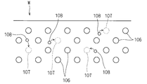
本実施形態においては、イオン注入によって空孔を形成した半導体ウェハーWの表面にドーパントを注入し、その半導体ウェハーWに対してフラッシュランプアニールを行っている。図9は、空孔が形成された半導体ウェハーW中におけるドーパントの挙動を説明する模式図である。半導体ウェハーWはゲルマニウムの単結晶にて形成されている。単結晶ゲルマニウムの結晶構造はダイヤモンド構造である。ダイヤモンド構造の結晶格子点のそれぞれにゲルマニウム原子106が配置されて単結晶ゲルマニウムが構成される。
In the present embodiment, a dopant is implanted into the surface of the semiconductor wafer W in which holes are formed by ion implantation, and flash lamp annealing is performed on the semiconductor wafer W. FIG. 9 is a schematic diagram for explaining the behavior of the dopant in the semiconductor wafer W in which holes are formed. The semiconductor wafer W is formed of a germanium single crystal. The crystal structure of single crystal germanium is a diamond structure. A
本実施形態では、ドーパントを注入する前に半導体ウェハーWの表面にゲルマニウムのイオンを注入して平衡濃度よりも高濃度の空孔107を形成している。そして、高濃度の空孔107を形成した半導体ウェハーWの表面にドーパントとしてボロン108を注入している。打ち込まれた直後のボロン108はゲルマニウムの結晶と整合しておらず、結晶中の適当な位置にランダムに分散している。
In this embodiment, before the dopant is implanted, germanium ions are implanted into the surface of the semiconductor wafer W to form
このような半導体ウェハーWの表面にフラッシュランプFLからフラッシュ光を照射してフラッシュランプアニールを行うと、打ち込まれたボロン108が空孔107に入り込んで活性化されることとなる。従って、ドーパント注入前に高濃度の空孔107が存在していると、アニール処理時におけるドーパントの活性化率が高くなる。ドーパント注入前の空孔107の濃度はゲルマニウムイオン注入時のドーズ量によって規定される。
When flash lamp annealing is performed by irradiating the surface of the semiconductor wafer W with flash light from the flash lamp FL, the implanted
図10は、ゲルマニウムイオン注入時のドーズ量とドーパントの活性化率との相関を示す図である。同図の横軸には、ドーパント注入前のゲルマニウムイオン注入時におけるゲルマニウムイオンのドーズ量を示している。ドーズ量とは、単位面積当たりに注入されたイオンの個数である。また、同図の縦軸には、アニール処理終了後に測定した半導体ウェハーWの表面のシート抵抗値を示している。この処理後のシート抵抗値が低いほど、ドーパントの活性化率が高く良好な活性化処理が行われたとみなすことができる。 FIG. 10 is a diagram showing the correlation between the dose amount at the time of germanium ion implantation and the activation rate of the dopant. The horizontal axis of the figure shows the dose amount of germanium ions at the time of germanium ion implantation before dopant implantation. The dose amount is the number of ions implanted per unit area. In addition, the vertical axis of the figure shows the sheet resistance value of the surface of the semiconductor wafer W measured after the annealing process is completed. It can be considered that the lower the sheet resistance value after the treatment, the higher the activation rate of the dopant and the better the activation treatment.
図10は、ゲルマニウムのイオンを注入して空孔107を形成した半導体ウェハーWの表面にドーパントとしてボロン108を注入してフラッシュランプアニールを行った結果を示す。フラッシュランプアニール時における半導体ウェハーWの表面の最高到達温度である処理温度T2が590℃の結果を丸で示し、処理温度T2が700℃の結果を三角で示し、処理温度T2が760℃の結果をばつ印で示している。なお、これら三種の結果について、処理温度T2以外の他の条件が同じであることは勿論である。
FIG. 10 shows the result of performing flash lamp annealing by implanting
図10に示すように、アニール処理時の処理温度T2に関わらず、ドーパント注入前のイオン注入時におけるゲルマニウムイオンのドーズ量が多くなるほど、シート抵抗値が低下してボロン108の活性化率が高くなる傾向が認められる。ゲルマニウムのドーズ量が5.0×10¹³/cm2にまで増加したときに、シート抵抗値が最も低くなる。但し、ゲルマニウムのドーズ量がそれを超えて1.0×1015/cm2程度にまで増加すると、逆にシート抵抗値が上昇している。
As shown in FIG. 10, the sheet resistance value decreases and the activation rate of
これは、ゲルマニウムのドーズ量が1.0×10¹⁵/cm2程度にまで増加すると、半導体ウェハーWの表面近傍におけるゲルマニウムの結晶がアモルファス化されてしまい、却ってドーパントであるボロン108の活性化が阻害されることによるものである。ゲルマニウムのドーズ量が5.0×1013/cm2以下であっても、ゲルマニウム結晶のアモルファス化は生じるのであるが、アモルファス化は半導体ウェハーWの表面の極浅い領域に留まり、ドーパントが注入される深さの領域はアモルファス化されずに空孔107が形成される。しかし、ゲルマニウムのドーズ量が1.0×1015/cm2程度にまで増加すると、ドーパントであるボロン108が注入される深さの領域までアモルファス化されてしまうのである。
This is because when the dose of germanium is increased to about 1.0 × 10 15 / cm 2 , germanium crystals in the vicinity of the surface of the semiconductor wafer W are amorphized, and on the contrary, the
換言すれば、空孔107を形成するためのゲルマニウムイオン注入時のドーズ量は、ドーパント注入時にドーパントであるボロン108が注入される半導体ウェハーWの表面からの深さ位置がアモルファス化されてしまうドーズ量未満とする必要がある。そのようにすれば、ボロン108が注入される深さの領域はアモルファス化されずに空孔107が形成されてボロン108の活性化率が向上することとなる。
In other words, the dose amount at the time of germanium ion implantation for forming the
また、図10に示すように、ゲルマニウムのドーズ量が5.0×10¹³/cm2以下であれば、ゲルマニウムのドーズ量とシート抵抗値との間に相関関係が認められる。このことは、ゲルマニウムのドーズ量を調整することによって、ドーパントの活性化率を適正な値に制御できることを示している。すなわち、ゲルマニウムイオン注入時のドーズ量を適宜に調整することによって、所望のドーパントの活性化率を得ることができるのである。 Further, as shown in FIG. 10, when the germanium dose is 5.0 × 10 13 / cm 2 or less, a correlation is recognized between the germanium dose and the sheet resistance value. This indicates that the activation rate of the dopant can be controlled to an appropriate value by adjusting the dose of germanium. That is, a desired dopant activation rate can be obtained by appropriately adjusting the dose at the time of germanium ion implantation.
以上、本発明の実施の形態について説明したが、この発明はその趣旨を逸脱しない限りにおいて上述したもの以外に種々の変更を行うことが可能である。例えば、上記実施形態においては、ゲルマニウムの半導体ウェハーWであったが、これに限定されるものではなく、シリコンまたはシリコンゲルマニウムの半導体ウェハーWであっても良い。シリコンまたはシリコンゲルマニウムの半導体ウェハーWの場合であっても、イオン注入によって空孔を形成した半導体ウェハーWの表面にドーパントを注入し、その半導体ウェハーWに対してフラッシュランプアニールを行うことにより、上記実施形態と同様の作用・効果を得ることができる。 While the embodiments of the present invention have been described above, the present invention can be modified in various ways other than those described above without departing from the spirit of the present invention. For example, in the above-described embodiment, the germanium semiconductor wafer W is used. However, the semiconductor wafer W is not limited to this, and may be a silicon or silicon germanium semiconductor wafer W. Even in the case of a semiconductor wafer W of silicon or silicon germanium, the dopant is implanted into the surface of the semiconductor wafer W in which holes are formed by ion implantation, and flash lamp annealing is performed on the semiconductor wafer W, thereby The same operation and effect as the embodiment can be obtained.
シリコンまたはシリコンゲルマニウムの半導体ウェハーWであれば、空孔を形成するためのイオン注入時にシリコンまたはゲルマニウムのイオンを注入するのが好ましい。また、半導体ウェハーWがシリコン、ゲルマニウムまたはシリコンゲルマニウムのいずれであっても、空孔を形成するためのイオン注入時のイオン源としてヘリウム(He)、アルゴン(Ar)、キセノン(Xe)等の不活性ガスを用いるようにしても良い。 In the case of a silicon or silicon germanium semiconductor wafer W, it is preferable to implant silicon or germanium ions at the time of ion implantation for forming vacancies. Further, regardless of whether the semiconductor wafer W is silicon, germanium, or silicon germanium, helium (He), argon (Ar), xenon (Xe), or the like is used as an ion source at the time of ion implantation for forming vacancies. An active gas may be used.
さらには、半導体ウェハーWがシリコン、ゲルマニウムまたはシリコンゲルマニウムのいずれであっても、空孔を形成するためのイオン注入時に比較的質量の大きなドーパントのイオンを半導体ウェハーWの表面に注入してダメージを与えるようにしても良い。比較的質量の大きなドーパントとしては、n型半導体を作成する場合にはヒ素(As)やアンチモン(Sb)を用いることができ、p型半導体を作成する場合にはガリウム(Ga)やインジウム(In)を用いることができる。 Furthermore, even if the semiconductor wafer W is silicon, germanium or silicon germanium, ions of a dopant having a relatively large mass are implanted into the surface of the semiconductor wafer W at the time of ion implantation for forming vacancies. You may make it give. As a dopant having a relatively large mass, arsenic (As) or antimony (Sb) can be used when forming an n-type semiconductor, and gallium (Ga) or indium (In) when forming a p-type semiconductor. ) Can be used.
このような比較的質量の大きなドーパントを半導体ウェハーWの表面に注入することによって上記実施形態と同様に半導体ウェハーWの表面におけるゲルマニウムの単結晶中に空孔を形成することができる。また、空孔を形成すると同時にドーパントの注入も行われることとなる。すなわち、空孔形成のためのイオン注入とドーパント注入とが同時に並行して行われることとなり、イオン注入工程を1回で完了させることができ、処理時間を短縮することができる。なお、リンやボロンは質量が比較的小さいため、空孔を形成するためのイオン種として用いることはできない。 By injecting such a dopant having a relatively large mass into the surface of the semiconductor wafer W, vacancies can be formed in the germanium single crystal on the surface of the semiconductor wafer W as in the above embodiment. In addition, the dopant is implanted simultaneously with the formation of the holes. That is, ion implantation for forming holes and dopant implantation are simultaneously performed in parallel, so that the ion implantation process can be completed in one time, and the processing time can be shortened. Since phosphorus and boron have a relatively small mass, they cannot be used as ion species for forming vacancies.
また、上記実施形態では、図9において半導体ウェハーWの表面にイオン注入を行って空孔107を形成する空孔形成工程を先に行った後、これに続いて半導体ウェハーW表面にドーパントであるボロン108を注入するドーパント注入工程を行うようにしていたが、これらの工程の順序はこれに限られるものではなく、半導体ウェハーW表面にドーパントを注入するドーパント注入工程を先に行った後、半導体ウェハーWの表面にイオン注入を行って空孔107を形成する空孔形成工程を行うようにしても良い。かかる場合でも、その後のドーパント活性化のための半導体ウェハーWの表面を加熱するアニール工程を実施することにより、打ち込まれたドーパントが空孔107に入り込んで活性化され、高い活性化率を得る処理を行うことができる。要は、ドーパント活性化のためのアニール工程の前に、順序は問わず空孔形成工程とドーパント注入工程とを行うようにすれば良いのである。
Moreover, in the said embodiment, after performing the hole formation process which ion-implants in the surface of the semiconductor wafer W in FIG. 9 and forms the
また、上記実施形態においては、ドーパント活性化のための熱処理をフラッシュランプアニールによって行っていたが、これに限定されるものではなく、例えば、スパイクアニールやレーザーアニール等の短時間にて処理温度T2にまで加熱できるアニール処理によって行うようにしても良い。 In the above embodiment, the heat treatment for activating the dopant is performed by flash lamp annealing. However, the present invention is not limited to this, and for example, the processing temperature T2 can be achieved in a short time such as spike annealing or laser annealing. It is also possible to carry out the annealing process that can be heated up to.
また、上記実施形態においては、チャンバー6内を常圧として基板Wの加熱処理を行っていたが、チャンバー6内を減圧して予備加熱およびフラッシュ加熱を行うようにしても良い。具体的には、チャンバー6内の圧力が20Pa〜大気圧(約101325Pa)の範囲内で基板Wの予備加熱およびフラッシュ加熱を行うようにしても良い。
Further, in the above embodiment, the heat treatment of the substrate W is performed with the inside of the
また、上記実施形態においては、フラッシュ加熱部5に30本のフラッシュランプFLを備えるようにしていたが、これに限定されるものではなく、フラッシュランプFLの本数は任意の数とすることができる。また、フラッシュランプFLはキセノンフラッシュランプに限定されるものではなく、クリプトンフラッシュランプであっても良い。また、ハロゲン加熱部4に備えるハロゲンランプHLの本数も40本に限定されるものではなく、任意の数とすることができる。
In the above embodiment, the
また、上記実施形態においては、ハロゲンランプHLからのハロゲン光照射によって基板Wを予備加熱するようにしていたが、予備加熱の手法はこれに限定されるものではなく、ホットプレートに載置することによって基板Wを予備加熱するようにしても良い。 In the above embodiment, the substrate W is preheated by irradiation with halogen light from the halogen lamp HL. However, the preheating method is not limited to this, and the substrate W is placed on a hot plate. Thus, the substrate W may be preheated.
1 熱処理装置
3 制御部
4 ハロゲン加熱部
5 フラッシュ加熱部
6 チャンバー
7 保持部
65 熱処理空間
74 サセプタ
75 保持プレート
77 基板支持ピン
93 コンデンサ
95 電源ユニット
96 IGBT
106 ゲルマニウム原子
107 空孔
108 ボロン
120 放射温度計
FL フラッシュランプ
HL ハロゲンランプ
W 半導体ウェハー
DESCRIPTION OF
106
Claims (5)
半導体基板の表面にイオン注入を行って当該表面の結晶中に空孔を形成する空孔形成工程と、
前記半導体基板の表面にドーパントを注入するドーパント注入工程と、
前記半導体基板の表面を加熱して前記ドーパントを活性化させるアニール工程と、
を備えることを特徴とするドーパント導入方法。 A dopant introduction method in which a dopant is injected into a semiconductor substrate and activated,
A vacancy forming step in which ions are implanted into the surface of the semiconductor substrate to form vacancies in the crystal of the surface; and
A dopant injection step of injecting a dopant into the surface of the semiconductor substrate;
An annealing step of activating the dopant by heating the surface of the semiconductor substrate;
A dopant introduction method characterized by comprising:
前記空孔形成工程でのイオン注入のドーズ量は、前記ドーパント注入工程にて前記ドーパントが注入される前記半導体基板の表面からの深さ位置がアモルファス化されるドーズ量未満とすることを特徴とするドーパント導入方法。 The dopant introduction method according to claim 1,
The dose amount of the ion implantation in the vacancy forming step is less than the dose amount at which the depth position from the surface of the semiconductor substrate into which the dopant is implanted in the dopant implantation step is amorphized. Dopant introduction method.
前記空孔形成工程でのイオン注入にて前記ドーパントを前記半導体基板の表面に注入して前記空孔形成工程と前記ドーパント注入工程とを並行して行うことを特徴とするドーパント導入方法。 In the dopant introduction method according to claim 1 or 2,
A dopant introduction method, wherein the dopant is implanted into the surface of the semiconductor substrate by ion implantation in the vacancy formation step, and the vacancy formation step and the dopant implantation step are performed in parallel.
前記半導体基板は、ゲルマニウム、シリコンゲルマニウムまたはシリコンにて形成されることを特徴とするドーパント導入方法。 In the dopant introduction method according to any one of claims 1 to 3,
The semiconductor substrate is formed of germanium, silicon germanium or silicon.
前記アニール工程では、前記半導体基板の表面にフラッシュランプからフラッシュ光を照射して当該表面を加熱することを特徴とするドーパント導入方法。 In the dopant introduction method according to any one of claims 1 to 4,
In the annealing step, the surface of the semiconductor substrate is irradiated with flash light from a flash lamp to heat the surface.
Priority Applications (1)
| Application Number | Priority Date | Filing Date | Title |
|---|---|---|---|
| JP2016160377A JP2018029128A (en) | 2016-08-18 | 2016-08-18 | Dopant introduction method |
Applications Claiming Priority (1)
| Application Number | Priority Date | Filing Date | Title |
|---|---|---|---|
| JP2016160377A JP2018029128A (en) | 2016-08-18 | 2016-08-18 | Dopant introduction method |
Publications (1)
| Publication Number | Publication Date |
|---|---|
| JP2018029128A true JP2018029128A (en) | 2018-02-22 |
Family
ID=61248605
Family Applications (1)
| Application Number | Title | Priority Date | Filing Date |
|---|---|---|---|
| JP2016160377A Pending JP2018029128A (en) | 2016-08-18 | 2016-08-18 | Dopant introduction method |
Country Status (1)
| Country | Link |
|---|---|
| JP (1) | JP2018029128A (en) |
Cited By (1)
| Publication number | Priority date | Publication date | Assignee | Title |
|---|---|---|---|---|
| US11695046B2 (en) | 2020-12-07 | 2023-07-04 | Samsung Electronics Co., Ltd. | Semiconductor device with reduced contact resistance |
Citations (14)
| Publication number | Priority date | Publication date | Assignee | Title |
|---|---|---|---|---|
| JPS6190429A (en) * | 1984-10-09 | 1986-05-08 | Sharp Corp | Formation of junction layer |
| JPS62259435A (en) * | 1986-05-02 | 1987-11-11 | Nec Corp | Method and apparatus for annealing |
| JPH03174721A (en) * | 1989-09-08 | 1991-07-29 | Fujitsu Ltd | Manufacturing method of semiconductor device |
| JPH0594958A (en) * | 1991-10-02 | 1993-04-16 | Toshiba Corp | Method for manufacturing semiconductor device |
| JPH05275362A (en) * | 1992-03-25 | 1993-10-22 | Fujitsu Ltd | Method for manufacturing semiconductor device |
| JPH08181085A (en) * | 1994-12-21 | 1996-07-12 | Nec Corp | Method for manufacturing semiconductor device |
| JP2000349039A (en) * | 1999-06-02 | 2000-12-15 | Nec Corp | Manufacture of semiconductor device having shallow diffusion layer |
| JP2003347234A (en) * | 2002-05-27 | 2003-12-05 | Toyota Central Res & Dev Lab Inc | Method of manufacturing iii nitride film |
| JP2004186677A (en) * | 2002-11-07 | 2004-07-02 | Semiconductor Energy Lab Co Ltd | Evaluation method of semiconductor element, method of manufacturing the semiconductor element, design management system for device having the semiconductor element, dose control program for the semiconductor element, computer-readable recording medium storing the program, and dose control apparatus |
| JP2007500433A (en) * | 2003-07-28 | 2007-01-11 | インターナショナル・ビジネス・マシーンズ・コーポレーション | Method of slowing dopant diffusion in a semiconductor substrate and device manufactured thereby |
| JP2009182109A (en) * | 2008-01-30 | 2009-08-13 | Toshiba Corp | Semiconductor device |
| JP2009181977A (en) * | 2008-01-29 | 2009-08-13 | Toshiba Corp | Semiconductor device and semiconductor manufacturing method. |
| JP2010021525A (en) * | 2008-06-13 | 2010-01-28 | Toshiba Corp | Manufacturing method for semiconductor device |
| JP2013120823A (en) * | 2011-12-07 | 2013-06-17 | Dainippon Screen Mfg Co Ltd | Heat treatment method and heat treatment device |
-
2016
- 2016-08-18 JP JP2016160377A patent/JP2018029128A/en active Pending
Patent Citations (14)
| Publication number | Priority date | Publication date | Assignee | Title |
|---|---|---|---|---|
| JPS6190429A (en) * | 1984-10-09 | 1986-05-08 | Sharp Corp | Formation of junction layer |
| JPS62259435A (en) * | 1986-05-02 | 1987-11-11 | Nec Corp | Method and apparatus for annealing |
| JPH03174721A (en) * | 1989-09-08 | 1991-07-29 | Fujitsu Ltd | Manufacturing method of semiconductor device |
| JPH0594958A (en) * | 1991-10-02 | 1993-04-16 | Toshiba Corp | Method for manufacturing semiconductor device |
| JPH05275362A (en) * | 1992-03-25 | 1993-10-22 | Fujitsu Ltd | Method for manufacturing semiconductor device |
| JPH08181085A (en) * | 1994-12-21 | 1996-07-12 | Nec Corp | Method for manufacturing semiconductor device |
| JP2000349039A (en) * | 1999-06-02 | 2000-12-15 | Nec Corp | Manufacture of semiconductor device having shallow diffusion layer |
| JP2003347234A (en) * | 2002-05-27 | 2003-12-05 | Toyota Central Res & Dev Lab Inc | Method of manufacturing iii nitride film |
| JP2004186677A (en) * | 2002-11-07 | 2004-07-02 | Semiconductor Energy Lab Co Ltd | Evaluation method of semiconductor element, method of manufacturing the semiconductor element, design management system for device having the semiconductor element, dose control program for the semiconductor element, computer-readable recording medium storing the program, and dose control apparatus |
| JP2007500433A (en) * | 2003-07-28 | 2007-01-11 | インターナショナル・ビジネス・マシーンズ・コーポレーション | Method of slowing dopant diffusion in a semiconductor substrate and device manufactured thereby |
| JP2009181977A (en) * | 2008-01-29 | 2009-08-13 | Toshiba Corp | Semiconductor device and semiconductor manufacturing method. |
| JP2009182109A (en) * | 2008-01-30 | 2009-08-13 | Toshiba Corp | Semiconductor device |
| JP2010021525A (en) * | 2008-06-13 | 2010-01-28 | Toshiba Corp | Manufacturing method for semiconductor device |
| JP2013120823A (en) * | 2011-12-07 | 2013-06-17 | Dainippon Screen Mfg Co Ltd | Heat treatment method and heat treatment device |
Cited By (2)
| Publication number | Priority date | Publication date | Assignee | Title |
|---|---|---|---|---|
| US11695046B2 (en) | 2020-12-07 | 2023-07-04 | Samsung Electronics Co., Ltd. | Semiconductor device with reduced contact resistance |
| US12148800B2 (en) | 2020-12-07 | 2024-11-19 | Samsung Electronics Co., Ltd. | Semiconductor device with reduced contact resistance |
Similar Documents
| Publication | Publication Date | Title |
|---|---|---|
| JP6560550B2 (en) | Heat treatment method and heat treatment apparatus | |
| JP5951241B2 (en) | Heat treatment method and heat treatment apparatus | |
| JP6184697B2 (en) | Heat treatment apparatus and heat treatment method | |
| KR102151357B1 (en) | Dopant introduction method and thermal treatment method | |
| JP6473659B2 (en) | Heat treatment method and heat treatment apparatus | |
| JP6598630B2 (en) | Heat treatment method | |
| JP2017092102A (en) | Heat treatment method and heat treatment apparatus | |
| JP5507227B2 (en) | Heat treatment method and heat treatment apparatus | |
| JP6810578B2 (en) | Dopant introduction method and heat treatment method | |
| JP6839939B2 (en) | Heat treatment method | |
| CN107658219B (en) | Heat treatment method | |
| JP2013120823A (en) | Heat treatment method and heat treatment device | |
| JP2018101760A (en) | Thermal treatment method | |
| JP2012199470A (en) | Heat treatment method and heat treatment apparatus | |
| JP2018029128A (en) | Dopant introduction method | |
| US20170221715A1 (en) | Method for forming junction in semiconductor | |
| JP5797916B2 (en) | Heat treatment method and heat treatment apparatus | |
| JP6945703B2 (en) | Dopant introduction method and heat treatment method | |
| JP2012191095A (en) | Heat treatment method and heat treatment device | |
| JP2018098314A (en) | Thermal treatment method of silicon substrate | |
| JP2018022715A (en) | Method for dopant introduction | |
| JP5701651B2 (en) | Heat treatment method and heat treatment apparatus | |
| JP2012191102A (en) | Heat treatment method and heat treatment device | |
| JP2012191094A (en) | Heat treatment method and heat treatment device |
Legal Events
| Date | Code | Title | Description |
|---|---|---|---|
| A80 | Written request to apply exceptions to lack of novelty of invention |
Free format text: JAPANESE INTERMEDIATE CODE: A80 Effective date: 20160829 |
|
| A621 | Written request for application examination |
Free format text: JAPANESE INTERMEDIATE CODE: A621 Effective date: 20190624 |
|
| A977 | Report on retrieval |
Free format text: JAPANESE INTERMEDIATE CODE: A971007 Effective date: 20200422 |
|
| A131 | Notification of reasons for refusal |
Free format text: JAPANESE INTERMEDIATE CODE: A131 Effective date: 20200526 |
|
| A521 | Request for written amendment filed |
Free format text: JAPANESE INTERMEDIATE CODE: A523 Effective date: 20200722 |
|
| A02 | Decision of refusal |
Free format text: JAPANESE INTERMEDIATE CODE: A02 Effective date: 20200811 |