JP2017533725A - A microfluidic platform for investigating cell-based interactions - Google Patents
A microfluidic platform for investigating cell-based interactions Download PDFInfo
- Publication number
- JP2017533725A JP2017533725A JP2017526142A JP2017526142A JP2017533725A JP 2017533725 A JP2017533725 A JP 2017533725A JP 2017526142 A JP2017526142 A JP 2017526142A JP 2017526142 A JP2017526142 A JP 2017526142A JP 2017533725 A JP2017533725 A JP 2017533725A
- Authority
- JP
- Japan
- Prior art keywords
- microfluidic
- chip substrate
- microfluidic platform
- platform
- chip
- Prior art date
- Legal status (The legal status is an assumption and is not a legal conclusion. Google has not performed a legal analysis and makes no representation as to the accuracy of the status listed.)
- Granted
Links
Images


Classifications
-
- C—CHEMISTRY; METALLURGY
- C12—BIOCHEMISTRY; BEER; SPIRITS; WINE; VINEGAR; MICROBIOLOGY; ENZYMOLOGY; MUTATION OR GENETIC ENGINEERING
- C12M—APPARATUS FOR ENZYMOLOGY OR MICROBIOLOGY; APPARATUS FOR CULTURING MICROORGANISMS FOR PRODUCING BIOMASS, FOR GROWING CELLS OR FOR OBTAINING FERMENTATION OR METABOLIC PRODUCTS, i.e. BIOREACTORS OR FERMENTERS
- C12M23/00—Constructional details, e.g. recesses, hinges
- C12M23/02—Form or structure of the vessel
- C12M23/12—Well or multiwell plates
-
- B—PERFORMING OPERATIONS; TRANSPORTING
- B01—PHYSICAL OR CHEMICAL PROCESSES OR APPARATUS IN GENERAL
- B01L—CHEMICAL OR PHYSICAL LABORATORY APPARATUS FOR GENERAL USE
- B01L3/00—Containers or dishes for laboratory use, e.g. laboratory glassware; Droppers
- B01L3/50—Containers for the purpose of retaining a material to be analysed, e.g. test tubes
- B01L3/502—Containers for the purpose of retaining a material to be analysed, e.g. test tubes with fluid transport, e.g. in multi-compartment structures
- B01L3/5027—Containers for the purpose of retaining a material to be analysed, e.g. test tubes with fluid transport, e.g. in multi-compartment structures by integrated microfluidic structures, i.e. dimensions of channels and chambers are such that surface tension forces are important, e.g. lab-on-a-chip
- B01L3/502761—Containers for the purpose of retaining a material to be analysed, e.g. test tubes with fluid transport, e.g. in multi-compartment structures by integrated microfluidic structures, i.e. dimensions of channels and chambers are such that surface tension forces are important, e.g. lab-on-a-chip specially adapted for handling suspended solids or molecules independently from the bulk fluid flow, e.g. for trapping or sorting beads, for physically stretching molecules
-
- C—CHEMISTRY; METALLURGY
- C12—BIOCHEMISTRY; BEER; SPIRITS; WINE; VINEGAR; MICROBIOLOGY; ENZYMOLOGY; MUTATION OR GENETIC ENGINEERING
- C12M—APPARATUS FOR ENZYMOLOGY OR MICROBIOLOGY; APPARATUS FOR CULTURING MICROORGANISMS FOR PRODUCING BIOMASS, FOR GROWING CELLS OR FOR OBTAINING FERMENTATION OR METABOLIC PRODUCTS, i.e. BIOREACTORS OR FERMENTERS
- C12M23/00—Constructional details, e.g. recesses, hinges
- C12M23/02—Form or structure of the vessel
- C12M23/16—Microfluidic devices; Capillary tubes
-
- C—CHEMISTRY; METALLURGY
- C12—BIOCHEMISTRY; BEER; SPIRITS; WINE; VINEGAR; MICROBIOLOGY; ENZYMOLOGY; MUTATION OR GENETIC ENGINEERING
- C12M—APPARATUS FOR ENZYMOLOGY OR MICROBIOLOGY; APPARATUS FOR CULTURING MICROORGANISMS FOR PRODUCING BIOMASS, FOR GROWING CELLS OR FOR OBTAINING FERMENTATION OR METABOLIC PRODUCTS, i.e. BIOREACTORS OR FERMENTERS
- C12M23/00—Constructional details, e.g. recesses, hinges
- C12M23/22—Transparent or translucent parts
-
- C—CHEMISTRY; METALLURGY
- C12—BIOCHEMISTRY; BEER; SPIRITS; WINE; VINEGAR; MICROBIOLOGY; ENZYMOLOGY; MUTATION OR GENETIC ENGINEERING
- C12M—APPARATUS FOR ENZYMOLOGY OR MICROBIOLOGY; APPARATUS FOR CULTURING MICROORGANISMS FOR PRODUCING BIOMASS, FOR GROWING CELLS OR FOR OBTAINING FERMENTATION OR METABOLIC PRODUCTS, i.e. BIOREACTORS OR FERMENTERS
- C12M23/00—Constructional details, e.g. recesses, hinges
- C12M23/24—Gas permeable parts
-
- C—CHEMISTRY; METALLURGY
- C12—BIOCHEMISTRY; BEER; SPIRITS; WINE; VINEGAR; MICROBIOLOGY; ENZYMOLOGY; MUTATION OR GENETIC ENGINEERING
- C12M—APPARATUS FOR ENZYMOLOGY OR MICROBIOLOGY; APPARATUS FOR CULTURING MICROORGANISMS FOR PRODUCING BIOMASS, FOR GROWING CELLS OR FOR OBTAINING FERMENTATION OR METABOLIC PRODUCTS, i.e. BIOREACTORS OR FERMENTERS
- C12M23/00—Constructional details, e.g. recesses, hinges
- C12M23/40—Manifolds; Distribution pieces
-
- B—PERFORMING OPERATIONS; TRANSPORTING
- B01—PHYSICAL OR CHEMICAL PROCESSES OR APPARATUS IN GENERAL
- B01L—CHEMICAL OR PHYSICAL LABORATORY APPARATUS FOR GENERAL USE
- B01L2200/00—Solutions for specific problems relating to chemical or physical laboratory apparatus
- B01L2200/02—Adapting objects or devices to another
- B01L2200/025—Align devices or objects to ensure defined positions relative to each other
-
- B—PERFORMING OPERATIONS; TRANSPORTING
- B01—PHYSICAL OR CHEMICAL PROCESSES OR APPARATUS IN GENERAL
- B01L—CHEMICAL OR PHYSICAL LABORATORY APPARATUS FOR GENERAL USE
- B01L2200/00—Solutions for specific problems relating to chemical or physical laboratory apparatus
- B01L2200/06—Fluid handling related problems
- B01L2200/0684—Venting, avoiding backpressure, avoid gas bubbles
-
- B—PERFORMING OPERATIONS; TRANSPORTING
- B01—PHYSICAL OR CHEMICAL PROCESSES OR APPARATUS IN GENERAL
- B01L—CHEMICAL OR PHYSICAL LABORATORY APPARATUS FOR GENERAL USE
- B01L2300/00—Additional constructional details
- B01L2300/08—Geometry, shape and general structure
- B01L2300/0809—Geometry, shape and general structure rectangular shaped
-
- B—PERFORMING OPERATIONS; TRANSPORTING
- B01—PHYSICAL OR CHEMICAL PROCESSES OR APPARATUS IN GENERAL
- B01L—CHEMICAL OR PHYSICAL LABORATORY APPARATUS FOR GENERAL USE
- B01L2300/00—Additional constructional details
- B01L2300/08—Geometry, shape and general structure
- B01L2300/0861—Configuration of multiple channels and/or chambers in a single devices
- B01L2300/0874—Three dimensional network
-
- B—PERFORMING OPERATIONS; TRANSPORTING
- B01—PHYSICAL OR CHEMICAL PROCESSES OR APPARATUS IN GENERAL
- B01L—CHEMICAL OR PHYSICAL LABORATORY APPARATUS FOR GENERAL USE
- B01L2300/00—Additional constructional details
- B01L2300/12—Specific details about materials
Landscapes
- Health & Medical Sciences (AREA)
- Chemical & Material Sciences (AREA)
- Zoology (AREA)
- Life Sciences & Earth Sciences (AREA)
- Engineering & Computer Science (AREA)
- Bioinformatics & Cheminformatics (AREA)
- Organic Chemistry (AREA)
- Wood Science & Technology (AREA)
- Clinical Laboratory Science (AREA)
- General Health & Medical Sciences (AREA)
- Biochemistry (AREA)
- Microbiology (AREA)
- General Engineering & Computer Science (AREA)
- Biotechnology (AREA)
- Genetics & Genomics (AREA)
- Biomedical Technology (AREA)
- Sustainable Development (AREA)
- Dispersion Chemistry (AREA)
- Physics & Mathematics (AREA)
- Fluid Mechanics (AREA)
- Analytical Chemistry (AREA)
- Hematology (AREA)
- Chemical Kinetics & Catalysis (AREA)
- Apparatus Associated With Microorganisms And Enzymes (AREA)
- Micro-Organisms Or Cultivation Processes Thereof (AREA)
Abstract
本発明による細胞ベースの相互作用を調べるためのマイクロ流体プラットフォーム(10)は、適切な光学特性を備えた適切なプラスチック材料から作製されたチップ基体(12)を含む。チップ基体(12)は複数のポート(14)を有し、複数のポート(14)は、細胞が保持される培地を含有するためのマイクロ流体流路(16)と流体連通する。好ましくは、ガス透過性ラミネート(20)がチップ基体(12)の底面に接合される。各ポート14は、ポート(14)をマイクロ流体流路(16)と接続する内側入口(22)と、入口(22)に隣接して培地流体の小さな貯蔵部を含むためのトラフ(24)とを有し、使用中、内側入口を直接経由するのではなくトラフを経由して培地をマイクロ流体流路から吸引することができる。A microfluidic platform (10) for investigating cell-based interactions according to the present invention comprises a chip substrate (12) made from a suitable plastic material with suitable optical properties. The chip substrate (12) has a plurality of ports (14), and the plurality of ports (14) are in fluid communication with a microfluidic channel (16) for containing a medium in which cells are retained. Preferably, a gas permeable laminate (20) is bonded to the bottom surface of the chip substrate (12). Each port 14 has an inner inlet (22) connecting the port (14) with the microfluidic channel (16), and a trough (24) for containing a small reservoir of media fluid adjacent to the inlet (22). During use, the medium can be aspirated from the microfluidic channel via the trough rather than directly through the inner inlet.
Description
本発明は、3次元(3D)マイクロ環境において細胞を培養するために使用されるマイクロ流体技術に関し、より詳細には、非排他的に、マイクロ流体プラスチックデバイスに関する。 The present invention relates to microfluidic technology used for culturing cells in a three-dimensional (3D) microenvironment, and more particularly, non-exclusively, to a microfluidic plastic device.
マイクロ流体技術は、高解像度リアルタイム撮像、多数の連通細胞の種類ならびに流れおよび勾配の制御の可能性を提供しながら、使用者が、より生理学的な3次元(3D)マイクロ環境で細胞を培養することを可能にする。国際特許出願であるPCT/US2009/039434号は、3次元マイクロ流体プラットフォームおよびその使用方法を記載している。これらの先行技術のデバイスを作製するために使用される材料は、ポリジメチルシロキサン(PDMS)、光学的に透明でありかつガス透過性である成型可能シリコーンである。PDMSは、マイクロ流体デバイスを製造するためのソフトリソグラフィプロセスによる迅速なプロトタイピングに一般に使用される。しかしながら、PDMSは、BeebeらによってLab Chip,2012,12,1224-1237に詳細に概説される理由のため、細胞ベース用途に理想的な材料ではない。要約すると、欠点のいくつかは以下のものを含む:
・PDMSは、疎水性化合物のバルク吸収を起こしやすい透過性材料であり、疎水性薬物/タンパク質を調査する生物学的アッセイは、それらの効率的な濃縮がバルク吸収によって低下し得るので、影響を受けるだろう。
・PDMSは気化を起こしやすい。PDMSの水蒸気透過性は、使用される培地の体積が小さいマイクロ流体デバイスにおいて欠点である。気化は浸透圧の変化を引き起こす可能性があり、細胞挙動に影響を及ぼし得る。
・PDMSは、その疎水性を取り戻す。PDMSは通常、疎水性であり、表面の親水性を高めるためにプラズマで処理される。親水性表面は表面機能化およびマイクロ流路充填などのマイクロ流体内の特定のプロセスを促す。しかしながら、プラズマ処理されたPDMS表面は、バルクから表面へのポリマー鎖の拡散により、それらの疎水性を取り戻す。その後使用者は使用前にプラズマ処理を繰り返さなければならず、その不便さに加えて、多くの使用者はプラズマ室へ出入りできないかもしれない。
・PDMSは、大量生産に適していない。PDMSの製造サイクル時間は、その長い硬化および処理時間のため、許容できないほど長い。
Microfluidic technology allows users to cultivate cells in a more physiological three-dimensional (3D) microenvironment while providing the possibility of high-resolution real-time imaging, numerous communicating cell types and flow and gradient control Make it possible. International patent application PCT / US2009 / 039434 describes a three-dimensional microfluidic platform and methods of use thereof. The material used to make these prior art devices is polydimethylsiloxane (PDMS), a moldable silicone that is optically transparent and gas permeable. PDMS is commonly used for rapid prototyping with a soft lithography process to produce microfluidic devices. However, PDMS is not an ideal material for cell-based applications because of the reasons outlined in detail in Beebe et al. In Lab Chip, 2012, 12, 1224-1237. In summary, some of the drawbacks include:
PDMS is a permeable material that is prone to bulk absorption of hydrophobic compounds, and biological assays investigating hydrophobic drugs / proteins have an impact because their efficient enrichment can be reduced by bulk absorption. Will receive.
・ PDMS is liable to vaporize. The water vapor permeability of PDMS is a drawback in microfluidic devices where the volume of medium used is small. Vaporization can cause changes in osmotic pressure and can affect cell behavior.
PDMS regains its hydrophobicity. PDMS is usually hydrophobic and is treated with plasma to increase the hydrophilicity of the surface. The hydrophilic surface facilitates certain processes within the microfluid such as surface functionalization and microchannel filling. However, plasma treated PDMS surfaces regain their hydrophobicity by diffusion of polymer chains from the bulk to the surface. The user must then repeat the plasma treatment before use, and in addition to its inconvenience, many users may not be able to enter or exit the plasma chamber.
PDMS is not suitable for mass production. The manufacturing cycle time of PDMS is unacceptably long due to its long curing and processing time.
本発明は、PDMSから作製された先行技術のデバイスに関連する問題を起こしにくいプラスチック材料から作製された3次元マイクロ流体プラットフォームを提供することを目的として開発された。本発明のマイクロ流体プラットフォームはまた、その機能を改善する多数の他の有利な特徴を組み込んでもよい。 The present invention was developed with the objective of providing a three-dimensional microfluidic platform made from a plastic material that is less prone to problems associated with prior art devices made from PDMS. The microfluidic platform of the present invention may also incorporate a number of other advantageous features that improve its function.
本明細書における先行技術の文献の参照は、単に説明を目的として提供され、そのような先行技術がシンガポール国または他の場所における共通の一般知識の一部であるという認証とみなすべきでない。 References to prior art documents herein are provided for illustrative purposes only and should not be regarded as an authentication that such prior art is part of common general knowledge in Singapore or elsewhere.
本発明の一態様によれば、細胞ベースの相互作用を調べるためのマイクロ流体プラットフォームが提供され、プラットフォームは、
適切な光学特性を備えた適切なプラスチック材料から作製されたチップ基体であって、細胞が保持される培地を含有するためのマイクロ流体流路と流体連通する複数のポートを有するチップ基体、
を含む。
According to one aspect of the invention, a microfluidic platform for investigating cell-based interactions is provided, the platform comprising:
A chip substrate made of a suitable plastic material with suitable optical properties, the chip substrate having a plurality of ports in fluid communication with a microfluidic channel for containing a medium in which cells are retained;
including.
好ましくは、チップ基体は、射出成型可能であり光学的に透明であるエンジニアリングプラスチック材料から作製される。典型的に、プラスチック材料は、ポリカーボネート(PC)、ポリスチレン(PS)、ポリエチレン(PE)、環状オレフィンコポリマー(COC)、環状オレフィンポリマー(COP)からなる群から選択される。 Preferably, the chip substrate is made from an engineering plastic material that is injection moldable and optically transparent. Typically, the plastic material is selected from the group consisting of polycarbonate (PC), polystyrene (PS), polyethylene (PE), cyclic olefin copolymer (COC), cyclic olefin polymer (COP).
好ましくは、プラットフォームはさらに、チップ基体の底面に接合されたガス透過性ラミネートを含む。 Preferably, the platform further comprises a gas permeable laminate bonded to the bottom surface of the chip substrate.
好ましくは、ガス透過性ラミネートは、低いかさ密度のポリマーから作製される。典型的に、低いかさ密度のポリマーは、ポリメチルペンテン(PMP)およびポリ(1−トリメチルシリル−1−プロピン)(PTMSP)からなる群から、またはポリメチル化ポリ(ジフェニルアセチレン)などのポリメチル化ポリマーから、または他の手段を介して十分なガス透過性を達成するポリマーから選択される。典型的に、ラミネートは、ヒートラミネーション(heat lamination)、溶剤接合、接着(湿潤または乾燥接着剤による)によって、または、チップ基体およびラミネートそれぞれに使用される特定の材料に依存する他の手段によって、チップ基体に接合される。好ましくは、ガス透過性ラミネートは光学的に透明である。 Preferably, the gas permeable laminate is made from a low bulk density polymer. Typically, low bulk density polymers are from the group consisting of polymethylpentene (PMP) and poly (1-trimethylsilyl-1-propyne) (PTMSP) or from polymethylated polymers such as polymethylated poly (diphenylacetylene). Or selected from polymers that achieve sufficient gas permeability through other means. Typically, the laminate is by heat lamination, solvent bonding, adhesion (by wet or dry adhesive) or by other means depending on the specific materials used for the chip substrate and laminate respectively. Bonded to the chip substrate. Preferably the gas permeable laminate is optically transparent.
典型的に、チップ基体は、直線状の配列で配置された細長い構成の複数のマイクロ流体流路を有し、各マイクロ流体流路は隣接流路と実質的に平行である。好ましくは、各マイクロ流体流路はポートの対を有し、1つのポートがそれぞれ各端部に設けられている。好ましくは、全てのポートはチップ基体の上面に開口する。好ましくは、マイクロ流体流路は対になって配置され、それらの間に第3のマイクロ流体流路が設けられ、第3の流路は、マイクロ流体流路の対と第3のマイクロ流体流路との間の制御された流体連通を可能にするように配置される。典型的に、第3のマイクロ流体流路は、ヒドロゲルまたは他の細胞外マトリックスで充填される。好ましくは、マイクロ流体流路の全ては、チップ基体の底面に形成され、チップ基体の底面に接合されたガス透過性ラミネートが流路を取り囲む。 Typically, the chip substrate has a plurality of elongated microfluidic channels arranged in a linear array, each microfluidic channel being substantially parallel to an adjacent channel. Preferably, each microfluidic channel has a pair of ports, one port being provided at each end. Preferably, all ports open to the top surface of the chip substrate. Preferably, the microfluidic channels are arranged in pairs, and a third microfluidic channel is provided between them, and the third channel is composed of a pair of microfluidic channels and a third microfluidic channel. Arranged to allow controlled fluid communication between the channels. Typically, the third microfluidic channel is filled with a hydrogel or other extracellular matrix. Preferably, all of the microfluidic channels are formed on the bottom surface of the chip substrate, and a gas permeable laminate joined to the bottom surface of the chip substrate surrounds the channels.
有利に、チップ基体は、複数の貯蔵部がその上面に成型された状態で形成され、複数の貯蔵部はポートと流体連通しておらず、使用の際、各貯蔵部は、デバイス周囲に湿った環境を作り出すために、滅菌水、ヒドロゲルまたは他の物質を保持するように適合されている。 Advantageously, the chip substrate is formed with a plurality of reservoirs molded on its upper surface, the plurality of reservoirs are not in fluid communication with the port, and in use, each reservoir is wetted around the device. Adapted to retain sterile water, hydrogels or other materials to create a clean environment.
典型的に、チップ基体は、概ね細長い長方形の形態のものであり、そのポートはその長手方向縁部に沿って配置されている。 Typically, the chip substrate is in the form of a generally elongate rectangle with its ports disposed along its longitudinal edges.
本発明の別の態様によれば、細胞ベースの相互作用を調べるためのマイクロ流体プラットフォームを製造する方法が提供され、方法は、
適切な光学特性を備えた適切なプラスチック材料からチップ基体を成型するステップであって、チップ基体は、細胞が保持される培地を含有するためのマイクロ流体流路と流体連通する複数のポートを有するステップ、
を含む。
According to another aspect of the present invention, there is provided a method of manufacturing a microfluidic platform for investigating cell-based interactions, the method comprising:
Molding a chip substrate from a suitable plastic material with suitable optical properties, the chip substrate having a plurality of ports in fluid communication with a microfluidic channel for containing a medium in which cells are retained Step,
including.
好ましくは、チップ基体を成型するステップは、光学的に透明なエンジニアリングプラスチック材料を使用して射出成型することを伴う。典型的に、プラスチック材料は、ポリカーボネート(PC)、ポリスチレン(PS)、ポリエチレン(PE)、環状オレフィンコポリマー(COC)、および環状オレフィンポリマー(COP)からなる群から選択される。 Preferably, the step of molding the chip substrate involves injection molding using an optically clear engineering plastic material. Typically, the plastic material is selected from the group consisting of polycarbonate (PC), polystyrene (PS), polyethylene (PE), cyclic olefin copolymer (COC), and cyclic olefin polymer (COP).
典型的に、方法はさらに、ガス透過性ラミネートをチップ基体の底面に接合するステップを含む。 Typically, the method further includes bonding the gas permeable laminate to the bottom surface of the chip substrate.
好ましくは、ガス透過性ラミネートは、光学的に透明であり、および、低いかさ密度のポリマーから作製される。典型的に、低いかさ密度のポリマーは、ポリメチルペンテン(PMP)およびポリ(1−トリメチルシリル−1−プロピン)(PTMSP)、ポリメチル化ポリ(ジフェニルアセチレン)などのポリメチル化ポリマー、または他の手段を介して十分なガス透過性を達成するポリマーからなる群から選択される。 Preferably, the gas permeable laminate is optically transparent and made from a low bulk density polymer. Typically, low bulk density polymers are polymethylated polymers such as polymethylpentene (PMP) and poly (1-trimethylsilyl-1-propyne) (PTMSP), polymethylated poly (diphenylacetylene), or other means. Selected from the group consisting of polymers that achieve sufficient gas permeability through.
典型的に、ラミネートをチップ基体に接合するステップは、ヒートラミネーションによってラミネートをチップ基体にラミネートすることを伴う。あるいは、ラミネートをチップ基体に接合するステップは、溶剤接合、接着接合(湿潤または乾燥接着剤による)、または、チップ基体およびラミネートそれぞれに使用される特定の材料に依存する他の接合手段を伴う。 Typically, bonding the laminate to the chip substrate involves laminating the laminate to the chip substrate by heat lamination. Alternatively, the step of bonding the laminate to the chip substrate involves solvent bonding, adhesive bonding (with wet or dry adhesive), or other bonding means depending on the specific materials used for the chip substrate and the laminate, respectively.
本発明のさらなる態様によれば、細胞ベースの相互作用を調べるためのマイクロ流体プラットフォームが提供され、プラットフォームは、
細胞が保持される流体培地を含有するマイクロ流体流路と流体連通する複数のポートを有するチップ基体であって、各ポートが、ポートをマイクロ流体流路と接続する内側入口と、入口に隣接して培地の小さな貯蔵部を含むためのトラフとを有し、使用の際、内側入口を直接経由するのではなくトラフを経由して培地をマイクロ流体流路から吸引することができるチップ基体を含む。
According to a further aspect of the invention, there is provided a microfluidic platform for studying cell-based interactions, the platform comprising:
A chip substrate having a plurality of ports in fluid communication with a microfluidic channel containing a fluid medium in which cells are retained, each port adjacent to the inlet, an inner inlet connecting the port to the microfluidic channel And a trough for containing a small reservoir of medium, and in use, includes a chip substrate that can aspirate the medium from the microfluidic channel via the trough rather than directly through the inner inlet .
一実施形態において、入口はポートの中心に設けられ、トラフは入口を取り囲む環状の構成のものである。 In one embodiment, the inlet is in the center of the port and the trough is of an annular configuration that surrounds the inlet.
典型的に、トラフの底面は半円形の断面のものである。 Typically, the trough bottom has a semicircular cross section.
好ましくは、マイクロ流体プラットフォームのポートは、モジュール式アタッチメントインターフェースとして設計される。 Preferably, the port of the microfluidic platform is designed as a modular attachment interface.
有利に、ポートは、チューブコネクタおよびシリンジポンプなどの標準型ルアーフィッティングをマイクロ流体プラットフォームに取り付けるための汎用モジュール式ルアーコネクタを受け入れるように適合される。 Advantageously, the port is adapted to accept a universal modular luer connector for attaching standard luer fittings such as tube connectors and syringe pumps to the microfluidic platform.
有利には、複数のマイクロ流体チップを、単一のマイクロプレートホルダに受け入れて保持することができる。好ましくは、ホルダは、その上面に設けられた複数の内側貯蔵部を含み、複数の内側貯蔵部はチップと流体連通せず、使用の際、各貯蔵部は、チップの周囲に湿った環境を作り出すために、滅菌水、ヒドロゲルまたは他の物質を保持するように適合される。 Advantageously, a plurality of microfluidic chips can be received and held in a single microplate holder. Preferably, the holder includes a plurality of inner reservoirs provided on an upper surface thereof, and the plurality of inner reservoirs are not in fluid communication with the chip, and in use, each reservoir has a moist environment around the chip. Adapted to retain sterile water, hydrogel or other material for production.
本明細書を通じて、文脈が他の意味を要求しない限り、「含む(comprise)」という語または「含む(comprises)」または「含む(comprising)」などの変形は、記載された完全体(integer)または完全体の群の包含を意味するが他の完全体および完全体の群の排除を意味しないと理解される。同様に、「好ましくは(preferably)」という用語または「好ましい(preferred)」などの変形は、記載された完全体または完全体の群が望ましいが、本発明の実施に必須ではないことを意味すると理解される。 Throughout this specification, unless the context requires otherwise, the word “comprise” or variations such as “comprises” or “comprising” are inclusive of the described integers. Or is understood to mean the inclusion of a complete group, but not the exclusion of other complete and complete groups. Similarly, the term “preferably” or variations such as “preferred” mean that the described complete or complete group is preferred but not essential to the practice of the invention. Understood.
図面の簡単な説明
本発明の特性は、添付図面を参照する、単に例として与えられたマイクロ流体プラットフォームのいくつかの特定の実施形態の以下の詳細な記載からより深く理解されるであろう。
BRIEF DESCRIPTION OF THE DRAWINGS The characteristics of the present invention will be better understood from the following detailed description of some specific embodiments of a microfluidic platform, given by way of example only, with reference to the accompanying drawings, in which:
好ましい実施形態の詳細な説明
図1および2に示されるような、本発明による細胞ベースの相互作用を調べるためのマイクロ流体プラットフォーム10の好ましい実施形態は、適切な光学特性を備えた適切なプラスチック材料から作製されたチップ基体12を含む。チップ基体12は、複数のポート14を有し、複数のポート14は、細胞が保持される培地17を含有するためのマイクロ流体流路16と流体連通する。
Detailed Description of Preferred Embodiments As shown in FIGS. 1 and 2, a preferred embodiment of a
典型的に、チップ基体12は、直線状の配列で配置された細長い構成の複数のマイクロ流体流路16を有し、各マイクロ流体流路16は、図10および11で最も明確に見ることができるように、隣接流路と実質的に平行である。各マイクロ流体流路16は、図4で最も明確に見ることができるように、それぞれ各端部に設けられた第1および第2のポート14を有する。好ましくは、全てのポート14はチップ基体12の上面に開口する。典型的に、チップ基体12は、概ね細長い長方形の構成のものであり、ポート14はそのそれぞれの長手方向の縁部に沿って配置されている。チップ基体12の典型的な寸法は、長さ75mm、幅25mm、および深さ6mmである。マイクロ流体流路16は典型的に250マイクロメートルの深さである。
Typically, the
好ましくは、マイクロ流体流路16は、図10および11に示されるように、対16a、16bとして構成され、それらの間に第3のマイクロ流体流路16cが設けられている。第3の流路16cは、マイクロ流体流路16a、16bの対と、第3のマイクロ流体流路16cとの間の制御された流体連通を許容するように配置される。典型的に、第3のマイクロ流体流路16cは、ヒドロゲル18または他の細胞外マトリックスで充填される。
Preferably, the
好ましくは、チップ基体12は、射出成型可能であり光学的に透明であるエンジニアリングプラスチック材料から作製される。典型的に、プラスチック材料は(非制限的に)、ポリカーボネート(PC)、ポリスチレン(PS)、ポリエチレン(PE)、環状オレフィンコポリマー(COC)、環状オレフィンポリマー(COP)からなる群から選択される。
Preferably, the
ポリカーボネート、ポリスチレンなどのプラスチックは、大規模に細胞培養デバイスを作製するために歴史的に使用されてきた。伝統的な細胞培養デバイスは、大きな空気ヘッドスペースと培地体積とを有するフラスコまたは井戸であり、それによりガス交換は容易に達成される。しかしながら、マイクロ流体デバイスは、密閉流路内の小さな体積部分から構成され、ほとんどのプラスチックはガス不透過性であるのでガス交換は制限因子になる。この制限は、プラスチックチップ基体14をガス透過性ラミネート20と組み合わせることによって克服し得る。
Plastics such as polycarbonate and polystyrene have historically been used to make cell culture devices on a large scale. Traditional cell culture devices are flasks or wells with large air headspace and media volume, whereby gas exchange is easily achieved. However, microfluidic devices are composed of a small volume in a closed channel and gas exchange is a limiting factor because most plastics are gas impermeable. This limitation can be overcome by combining the
好ましくは、ガス透過性ラミネート20は光学的に透明であり、低いかさ密度のポリマーから作製される。典型的に、低いかさ密度のポリマーは、ポリメチルペンテン(PMP)およびポリ(1−トリメチルシリル−1−プロピン)(PTMSP)からなる群から、またはポリメチル化ポリ(ジフェニルアセチレン)などのポリメチル化ポリマーから、または他の手段を介して十分なガス透過性を達成するポリマーから選択される。好ましくは、マイクロ流体流路16の全ては、チップ基体12の底面に形成され、ガス透過性ラミネート20は、図2および11に示されるように、流路16を閉鎖するようにチップ基体の底面に接合される。典型的に、ラミネート20は、ヒートラミネーション、溶剤接合、接着(湿潤または乾燥接着剤による)によって、または、チップ基体12およびラミネート20それぞれに使用される特定の材料に依存する他の手段によって、チップ基体12に接合される。
Preferably, the gas
チップ基体12を完全にガス透過性ポリマーから作製することも可能である。そうすることで、ラミネート20およびチップ基体12の両方が同一の材料特性を有し得るので、より簡単な積層プロセスを実現するという利点が得られるかもしれない。しかしながら、酸素は(数十から数百マイクロメートルのオーダーの)薄いラミネートに対して(ミリメートルのオーダーの)厚いチップ基体全体に拡散する必要があるので、酸素利用可能性の大幅な増加はないかもしれない。特殊化されたガス透過性プラスチックは、同じく、それらを射出成型に適さなくする材料特性を有し得る。これらの理由から、好ましい実施形態において、チップ基体12は、標準的な射出成型可能プラスチックから作製され、デバイスは薄いガス透過性ラミネートで積層される。
It is also possible to make the
本発明のマイクロ流体プラットフォームまたはチップ10は、培養システム中の細胞の生体内挙動を再現することができる。マイクロ流体プラットフォームまたはチップ10の用途は(非制限的に)以下を含み得る:
・学問的および産業的研究開発用の研究ツール
・製薬会社での薬剤発見ツール
・臨床的治療を個々の患者に合わせるための補助ツール。
The microfluidic platform or
• Research tools for academic and industrial R & D • Drug discovery tools at pharmaceutical companies • Auxiliary tools to tailor clinical treatment to individual patients.
使い易さは学問的研究開発顧客分野にとって重要な差別化要因である。PDMSチップ製作の不便さに加えて、使用者は以下のものを含む他の使用上の難題に直面している。 Ease of use is an important differentiator for academic R & D customer areas. In addition to the inconvenience of PDMS chip fabrication, users are faced with other usage challenges including:
培地の日々の交換−マイクロ流体デバイスは、各流路内に小さな培地体積(典型的に数十マイクロリットル)を有する。これは、培地の養分含有量が、培養された細胞によって急速に使い果たされ、培地を日々交換しなければならないことを意味する。使用者は多数の小さなデバイスの培地を交換しなければならないので、プロセスは単純、迅速かつ耐エラー性である必要がある。培地は典型的に、減圧吸引に取り付けられたピペット先端によってマイクロ流体流路から吸引される。発生する共通のエラーは、過大な減圧力が適用される場合の過吸引であり、この結果、細胞は培地とともに流路から吸引され、細胞損失/死滅が生じる。 Daily exchange of media—Microfluidic devices have a small media volume (typically tens of microliters) in each channel. This means that the nutrient content of the medium is quickly depleted by the cultured cells and the medium must be changed daily. Since the user has to change the medium of many small devices, the process needs to be simple, quick and error-resistant. The medium is typically aspirated from the microfluidic channel by a pipette tip attached to a vacuum suction. A common error that occurs is over-suction when an excessive decompression force is applied, which results in cells being aspirated from the flow path along with the media, resulting in cell loss / death.
柔軟性:研究者は、例えば培地の条件を変更するために他のデバイスおよび装置を培養システムに接続することによって、異なる設定で実験する柔軟性を評価する。現在の使用者は、自力で接続を作り出す必要があり、これは不便かつ信頼性を欠く可能性がある。 Flexibility: Researchers evaluate the flexibility to experiment with different settings, for example by connecting other devices and equipment to the culture system to change the conditions of the medium. Current users need to create connections on their own, which can be inconvenient and unreliable.
取扱い:使用者は、彼らの培養器の制限された空間の最適な使用を実行するマイクロ流体チップを要望する。チップはまた、溢流も汚染もなく、組織培養装置へおよび様々な顕微鏡プラットフォームへ運ばれなければならない。(例えばロボットプラットフォームによる)デバイスの自動取扱いは、微量検定板のような特定の形態の因子に制限される。 Handling: Users want a microfluidic chip that performs optimal use of the limited space of their incubator. The tip must also be transported to tissue culture equipment and to various microscope platforms without overflow or contamination. Automatic handling of devices (eg, by robotic platforms) is limited to specific forms of factors such as micro assay plates.
気化制御−マイクロ流体デバイスは小さい培地体積を有するので、気化損失により培地浸透圧にかなりの変化が引き起こされ、その結果、望ましくない培養条件がもたらされる。使用者は、気化に対抗するように培養器内の湿度室を設定する必要がある。 Vaporization control-Since microfluidic devices have a small media volume, loss of vaporization causes a significant change in media osmotic pressure, resulting in undesirable culture conditions. The user needs to set the humidity chamber in the incubator to counter the vaporization.
上で概説した使用上の難題を克服するために、数多くの刷新がマイクロ流体プラットフォームまたはチップ10の好ましい実施形態に組み込まれた。これらの追加的な刷新をここで詳細に説明する。
Numerous innovations have been incorporated into the preferred embodiment of the microfluidic platform or
A.過吸引のない急速な培地の交換
従来技術のマイクロ流体ポート設計は形状が円筒型であり、これは流路に直接つながっている(図3参照)。培地を交換する間の減圧吸引により、細胞が流路から吸引される可能性がある。改善されたポート設計は、内側入口よりも深い内側トラフを形成することを伴う(図4参照)。各ポート14は、ポート14をマイクロ流体流路16と接続する内側入口22と、入口22に隣接して培地流体の小さな貯蔵部を含むためのトラフ24とを有し、使用の際、内側入口22を直接経由するのではなくトラフ24を経由して培地をマイクロ流体流路16から吸引することができる。
A. Rapid media replacement without oversuction The prior art microfluidic port design is cylindrical in shape, which is directly connected to the flow path (see FIG. 3). Cells may be aspirated from the flow path by vacuum aspiration while changing the medium. The improved port design involves forming an inner trough that is deeper than the inner inlet (see FIG. 4). Each
示される実施形態では、入口22はポート14の中心に設けられ、トラフ24は(図4の断面に示されるように)入口を同心円状に囲む環状の構造である。あるいは、トラフ24は、依然として入口22に隣接して配置される異なる構造のものであってもよい。典型的に、トラフの底面は半円状の断面である。
In the embodiment shown, the
図4に示されるようにトラフ24内に配置されたガラス/ピペット先端26を介した減圧の適用により、培地流体の除去が生じ、トラフ内の培地が完全に除去されると停止する。内側入口22のより高い高さのため、流路内の培地および細胞は、ピペット先端がトラフ24内にどれほどの時間維持されていようと、減圧吸引による影響を受けないであろう。次いで新しい培地を流路16の一方の側のポート(「上流」ポート)に追加して、チャネルに流し、古い培地と置き換えることができる。マイクロ流体システムの表面張力効果の結果として、少量の新しい培地を下流ポートに追加する必要があり得、その結果、下流入口の表面張力に打ち勝って流入流を許容することができる。
Application of reduced pressure through a glass /
B.モジュール式ルアーコネクタおよびインターフェースによる柔軟性
チップ流路ポート14は好ましくはモジュール式アタッチメントインターフェースとして設計される。AIMの汎用ルアーロックコネクタ30(図5に示される)は、使用者が(例えばチューブコネクタおよびシリンジポンプを取り付けるために)標準型ルアーフィッティングをマイクロ流体チップ10に取り付けることを可能にする。AIMによって開発される将来の付属品は、ポート14に直接、または汎用コネクタを介して接続する可能性がある。図5は、マイクロ流体プラットフォーム10の各ポート14に接続された複数のモジュール式コネクタ30を示す。図5は、ルアースリップおよびルアーロック接続用コネクタ(左)と、ルアースリップおよびルアーロックシリンジに取り付けられたコネクタ(右)の両方を示す。
B. Flexibility with modular luer connectors and interfaces The
他の製造業者による従来技術のアプローチは、チップに直接組み付けた別個の構成要素に基づく。これらコネクタ構成要素はチップから突出し、初期設定によってチップ内に含められている。本発明のモジュール設計は、2つの重要な利点を有する:
(i)マイクロ流体チップ10は単一材料から単一構成要素へより効率的に作製可能である。全ての使用者が他のデバイスに接続したいわけではない。このような使用者は、基本チップ10をそれ自体で使用する選択肢を有し得る。他のデバイスへの接続を必要とする他の使用者は、モジュール式ルアーコネクタを使用する別の選択肢を有する。この設計アプローチは製造業者および使用者の両者により経済的な認識を抱かせる、というのも、コアプラットフォーム(すなわちチップ)はより簡単に製造できるようになる一方で、使用者コミュニティはより低い価格ベースを得、さらにはより多くの選択肢を有するようになるからである。
(ii)ポートは二重の役割を果たす。ポートは貯蔵部として機能し、接続を必要としない使用者に迅速な培地の交換を可能にする。シリンジポンプ等に接続することを必要とする他の使用者は、ポートを接続インターフェースとして使用するだろう。後者の使用者グループは、ポンプなどの接続された装置を使用することによって培地を交換するであろうし、そのため迅速な培地交換機能は必要ないことを注記しておく。このアプローチは、チップ上の限定された不動産の使用を最適化する。それはまた、将来の付属品を、ポートのトラフおよび入口にぴったり合ったインターフェースを用いて直接チップに取り付けることを可能にし、他の製造業者が今日使用する余分な構成要素を排除する。
Prior art approaches by other manufacturers are based on discrete components assembled directly on the chip. These connector components protrude from the chip and are included in the chip by default. The modular design of the present invention has two important advantages:
(I) The
(Ii) The port plays a dual role. The port functions as a reservoir and allows users who do not need a connection to quickly change media. Other users who need to connect to a syringe pump or the like will use the port as a connection interface. Note that the latter group of users will change the medium by using a connected device such as a pump, so a rapid medium change function is not required. This approach optimizes the use of limited real estate on the chip. It also allows future accessories to be attached directly to the chip using an interface that fits well with the port trough and inlet, eliminating the extra components that other manufacturers use today.
C.SBS/ANSI準拠マイクロプレートホルダによる取扱いの改善
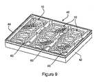
有利に複数のマイクロ流体チップ10を図7および9に示されるように単一マイクロプレートホルダ40に受け入れて保持することができる。マイクロプレートホルダ40の示される実施形態は、側壁および略平坦な基部を有するトレイ42と、それとの接続に設けられた複数の区画46とを含む。トレイ42内の各区画46は、マイクロ流体チップ10を受け入れるように適合されている。示される実施形態では、トレイ42は、最大3つの流体チップ10を受け入れるように設計されている。好ましくは、ホルダ40はさらに、マイクロ流体チップ10を包み込むようにトレイの上面に受け止められるカバー44を含む。有利にカバー44は実質的に透明である。有利に複数のホルダ40は積み重ね可能でもある。
C. Improved handling with SBS / ANSI compliant microplate holders Advantageously, multiple
顕微鏡スライドおよび微量検定板などの標準形状因子は生物学的および薬学的研究業界で普及している。チップおよびホルダの両方は、デバイスが既存ワークフローに適合するように、これらの既存の基準に適合すべく設計される。ホルダは標準型顕微鏡プラットフォームにも合うであろうし、細胞培養器内の作業スペースを最大化するために積み重ねることができる。ホルダは、微量検定板のSBS/ANSI規格に適合するようにチップ流路ポート14を位置付けるように設計され、その結果、ホルダは自動プレート充填/取扱いシステムに対応できるようになる。そのようなシステムはマイクロプレート中の井戸を充填するために作製され、充填位置が正確に位置付けられることを必要とする。この設計アプローチのさらなる利点は、学問的研究所での手作業に適したデバイスが、産業的な自動化された設定においても展開できることである。
Standard form factors such as microscope slides and micro assay plates are prevalent in the biological and pharmaceutical research industries. Both tips and holders are designed to meet these existing standards so that the device fits into existing workflows. The holder will also fit a standard microscope platform and can be stacked to maximize the working space in the cell incubator. The holder is designed to position the
D.チップおよびホルダ設計による湿度制御
マイクロ流体システムの使用者は、気化を制限するためにそれらのデバイスを湿度室の中に配置しなければならないことがよくある。有利にチップ10およびホルダ40の両方は、デバイス周囲(およびホルダ内)に湿った環境を作り出すために、滅菌水、ヒドロゲル(例えばアガロース、ポリアクリルアミド等)、または他の物質で満たすことができる内蔵型貯蔵部(図8および9参照)を有する。このアプローチは、別個の湿度室を設定する必要性を排除する。これはまた、デバイスを撮像プラットフォーム上に移動するとき、湿潤状態の容易な取扱いおよび保持を促す、というのも、湿潤機能がチップおよびホルダ自体に形成されているからである。
D. Humidity control by chip and holder design Microfluidic system users often have to place their devices in a humidity chamber to limit vaporization. Advantageously, both
図8で最も明確に見ることができるように、チップ基体12は、複数の貯蔵部50がその上面に成型された状態で形成される。貯蔵部50はポート14と流体連通していない。使用の際、各貯蔵部は、デバイス周囲に湿った環境を作り出すために、滅菌水、ヒドロゲルまたは他の物質を保持するために使用可能である。
As can be seen most clearly in FIG. 8, the
同様に、ホルダ40はさらに、図9で最も明確に見ることができるように、トレイ42内に設けられた複数の内側貯蔵部60を含む。貯蔵部60はチップ10と別個のものであり、またチップ10と流体連通していない。従って、使用の際、各貯蔵部60は、チップ10の周囲に湿った環境を作り出すために、滅菌水、ヒドロゲルまたは他の物質を保持するために使用可能である。
Similarly, the
マイクロ流体プラットフォームの好ましい実施形態を詳細に記載してきたので、それが以下のものを含む従来技術を上回る多数の利点を提供することは明白であろう。
(i)それはチップの基体にPDMSを使用することに関連する問題を克服する。
(ii)改善されたチップ流路ポートの設計は過吸引に関連する問題を取り除く。
(iii)チップはそれ自体で、またはモジュール式ルアーコネクタを使用して他のデバイスと一緒に使用可能である。
(iV)チップおよびホルダの両方は、微量検定板のSBS/ANSI規格に適合し、その結果、それらは自動プレート充填/取扱いシステムに対応できる。
(V)内蔵型貯蔵部はチップおよびホルダの両方が搭載型湿気制御を実現することを可能にする。
Having described in detail the preferred embodiment of the microfluidic platform, it will be clear that it offers a number of advantages over the prior art, including:
(I) It overcomes the problems associated with using PDMS on the chip substrate.
(Ii) Improved tip channel port design eliminates problems associated with oversuction.
(Iii) The chip can be used by itself or with other devices using a modular luer connector.
Both (iV) tips and holders meet the SBS / ANSI standard for micro assay plates so that they can accommodate automated plate filling / handling systems.
(V) The built-in storage allows both the chip and the holder to achieve on-board moisture control.
当業者には、本発明の基本的な発明概念から逸脱することなく、既に説明したものに加えて、前述の実施形態に様々な変更および改良を加えてもよいことが容易に明らかであろう。例えば、記載された実施形態における流体プラットフォームまたはチップにはそれぞれ3組のマイクロ流体流路が設けられている。しかしながら、チップは、任意の所望の数の流路を組み込むように、そして様々な構成でカスタム設計することができる。したがって、本発明の範囲は、記載される特定の実施形態に限定されないことが理解されよう。 It will be readily apparent to those skilled in the art that various changes and modifications may be made to the above-described embodiments in addition to those already described without departing from the basic inventive concept of the invention. . For example, each set of fluid platforms or chips in the described embodiments is provided with three sets of microfluidic channels. However, the chip can be custom designed to incorporate any desired number of channels and in various configurations. Therefore, it will be understood that the scope of the invention is not limited to the specific embodiments described.
Claims (31)
適切な光学特性を備えた適切なプラスチック材料から作製されたチップ基体であって、細胞が保持される培地を含有するためのマイクロ流体流路と流体連通する複数のポートを有するチップ基体、
を含むマイクロ流体プラットフォーム。 A microfluidic platform for investigating cell-based interactions,
A chip substrate made of a suitable plastic material with suitable optical properties, the chip substrate having a plurality of ports in fluid communication with a microfluidic channel for containing a medium in which cells are retained;
Including microfluidic platform.
適切な光学特性を備えた適切なプラスチック材料からチップ基体を成型するステップであって、前記チップ基体は、細胞が保持される培地を含有するためのマイクロ流体流路と流体連通する複数のポートを有するステップ、
を含む方法。 A method of manufacturing a microfluidic platform for investigating cell-based interactions comprising:
Molding a chip substrate from a suitable plastic material with suitable optical properties, the chip substrate having a plurality of ports in fluid communication with a microfluidic channel for containing a medium in which cells are retained; Having steps,
Including methods.
細胞が保持される流体培地を含有するマイクロ流体流路と流体連通する複数のポートを有するチップ基体であって、各ポートが、前記ポートを前記マイクロ流体流路と接続する内側入口と、前記入口に隣接して培地流体の小さな貯蔵部を含むためのトラフとを有し、使用中、前記内側入口を直接経由するのではなく前記トラフを経由して培地を前記マイクロ流体流路から吸引することができるチップ基体、
を含む、マイクロ流体プラットフォーム。 A microfluidic platform for investigating cell-based interactions,
A chip substrate having a plurality of ports in fluid communication with a microfluidic channel containing a fluid medium in which cells are retained, each port having an inner inlet connecting the port to the microfluidic channel; and the inlet A trough for containing a small reservoir of medium fluid adjacent to the medium, and in use, aspirate the medium from the microfluidic channel via the trough rather than directly via the inner inlet A chip substrate,
Including a microfluidic platform.
Applications Claiming Priority (3)
| Application Number | Priority Date | Filing Date | Title |
|---|---|---|---|
| US201462077942P | 2014-11-11 | 2014-11-11 | |
| US62/077,942 | 2014-11-11 | ||
| PCT/SG2015/050441 WO2016076795A1 (en) | 2014-11-11 | 2015-11-09 | Microfluidic platform for investigating cell-based interactions |
Publications (2)
| Publication Number | Publication Date |
|---|---|
| JP2017533725A true JP2017533725A (en) | 2017-11-16 |
| JP6857123B2 JP6857123B2 (en) | 2021-04-14 |
Family
ID=55954736
Family Applications (1)
| Application Number | Title | Priority Date | Filing Date |
|---|---|---|---|
| JP2017526142A Active JP6857123B2 (en) | 2014-11-11 | 2015-11-09 | Microfluidic platform for investigating cell-based interactions |
Country Status (9)
| Country | Link |
|---|---|
| US (1) | US10711234B2 (en) |
| EP (1) | EP3218300B1 (en) |
| JP (1) | JP6857123B2 (en) |
| KR (1) | KR102260910B1 (en) |
| CN (1) | CN107108199B (en) |
| CA (1) | CA3004596C (en) |
| DK (1) | DK3218300T3 (en) |
| SG (1) | SG11201809990TA (en) |
| WO (1) | WO2016076795A1 (en) |
Cited By (1)
| Publication number | Priority date | Publication date | Assignee | Title |
|---|---|---|---|---|
| WO2020095852A1 (en) * | 2018-11-07 | 2020-05-14 | ウシオ電機株式会社 | Cell culturing chip |
Families Citing this family (12)
| Publication number | Priority date | Publication date | Assignee | Title |
|---|---|---|---|---|
| SG11202003650PA (en) * | 2017-10-23 | 2020-05-28 | Nat Univ Singapore | Planar modular microfluidic system |
| WO2020090771A1 (en) * | 2018-10-29 | 2020-05-07 | 国立大学法人東京大学 | Artificial multilayer tissue culture device, and method for producing artificial multilayer tissue |
| KR20220052911A (en) | 2019-06-27 | 2022-04-28 | 에뮬레이트, 인크. | Dispensing compounds in microfluidic devices |
| TR201909710A2 (en) * | 2019-06-28 | 2021-01-21 | Koc Ueniversitesi | A MICROFLUID PLATFORM TO ENABLE CULTIVATION OF CELLS IN A THREE-DIMENSIONAL MICRO-PERIPHERAL |
| IL292337A (en) * | 2019-10-21 | 2022-06-01 | Flaskworks Llc | Cell culture systems and methods |
| EP3892713A1 (en) * | 2020-04-08 | 2021-10-13 | Cellectricon Ab | Multi-well plates for creation of high-density arrays of compartmentalized cell cultures for usage in high capacity applications |
| JP7543710B2 (en) * | 2020-06-04 | 2024-09-03 | ウシオ電機株式会社 | Microfluidic Devices |
| DE102021204675B4 (en) * | 2021-05-07 | 2023-05-17 | Lpkf Laser & Electronics Se | Device and method for cell cultivation |
| EP4289933A1 (en) | 2022-06-07 | 2023-12-13 | ibidi GmbH | Cell culture substrate |
| EP4536801A1 (en) | 2022-06-13 | 2025-04-16 | ETH Zurich | Collagen visualization on microfluidic device |
| US20240368514A1 (en) * | 2023-05-05 | 2024-11-07 | Kuhner Shaker Inc. | Sbs-format single, or dual, deep well stackable cell culture disposable well plate and closure |
| EP4481029A1 (en) | 2023-06-22 | 2024-12-25 | Cherry Biotech SAS | Method for controlling fluid displacement and gas(es) composition and/or ph in a cell culture device and corresponding cell culture system |
Citations (11)
| Publication number | Priority date | Publication date | Assignee | Title |
|---|---|---|---|---|
| US20020114739A1 (en) * | 2000-12-26 | 2002-08-22 | Weigl Bernard H. | Microfluidic cartridge with integrated electronics |
| JP2005027659A (en) * | 2003-06-20 | 2005-02-03 | Nitto Denko Corp | Cell microchip |
| US20050266582A1 (en) * | 2002-12-16 | 2005-12-01 | Modlin Douglas N | Microfluidic system with integrated permeable membrane |
| JP2006521829A (en) * | 2003-04-03 | 2006-09-28 | フルイディグム コーポレイション | Microfluidic device and method of use thereof |
| JP2009544043A (en) * | 2006-07-19 | 2009-12-10 | バイオセプト インコーポレイティッド | Detection or isolation of target molecules using a microchannel device |
| JP2012194062A (en) * | 2011-03-16 | 2012-10-11 | Tokyo Denki Univ | Microfluid chip and microfluid system using the same |
| WO2013019491A1 (en) * | 2011-08-01 | 2013-02-07 | Denovo Sciences | Cell capture system and method of use |
| JP2013076591A (en) * | 2011-09-30 | 2013-04-25 | Sumitomo Bakelite Co Ltd | Microchannel device and method for manufacturing the same |
| JP2013517809A (en) * | 2010-01-28 | 2013-05-20 | ザ リージェンツ オブ ザ ユニバーシティ オブ ミシガン | Suspended drop device, suspended drop system, and / or suspended drop method |
| JP2013538582A (en) * | 2010-09-29 | 2013-10-17 | マサチューセッツ インスティテュート オブ テクノロジー | Devices for high-throughput studies of cell-cell interactions |
| JP2014055940A (en) * | 2012-08-13 | 2014-03-27 | Canon Inc | Micro flow channel chip and manufacturing method thereof |
Family Cites Families (9)
| Publication number | Priority date | Publication date | Assignee | Title |
|---|---|---|---|---|
| US6090251A (en) | 1997-06-06 | 2000-07-18 | Caliper Technologies, Inc. | Microfabricated structures for facilitating fluid introduction into microfluidic devices |
| WO2000070350A1 (en) * | 1999-05-12 | 2000-11-23 | Cme Telemetrix Inc. | METHOD AND APPARATUS FOR RAPID MEASUREMENT OF HbA¿1c? |
| GB0321158D0 (en) * | 2003-09-10 | 2003-10-08 | Central Research Lab Ltd | Apparatus and method for handling cells,embryos or oocytes |
| WO2007002580A2 (en) * | 2005-06-23 | 2007-01-04 | Bioveris Corporation | Diagnostic as say system with multi -well reagent container |
| EP2268405B1 (en) * | 2008-02-27 | 2017-01-04 | Boehringer Ingelheim Microparts Gmbh | Apparatus for the separation of plasma |
| WO2009126524A2 (en) | 2008-04-08 | 2009-10-15 | Massachusetts Institute Of Technology | Three-dimensional microfluidic platforms and methods of use thereof |
| CN101827931A (en) * | 2008-08-29 | 2010-09-08 | 北京大学 | A microfluidic chip for accurately controllable cell culture |
| US20100056394A1 (en) | 2008-09-04 | 2010-03-04 | Chung Yuan Christian University | Mini Bio-Reactor |
| WO2010056755A2 (en) | 2008-11-11 | 2010-05-20 | Craig H Randall | Microfluidic embryo and gamete culture systems |
-
2015
- 2015-11-09 EP EP15859297.2A patent/EP3218300B1/en active Active
- 2015-11-09 CN CN201580072922.6A patent/CN107108199B/en active Active
- 2015-11-09 SG SG11201809990TA patent/SG11201809990TA/en unknown
- 2015-11-09 JP JP2017526142A patent/JP6857123B2/en active Active
- 2015-11-09 CA CA3004596A patent/CA3004596C/en active Active
- 2015-11-09 DK DK15859297.2T patent/DK3218300T3/en active
- 2015-11-09 WO PCT/SG2015/050441 patent/WO2016076795A1/en not_active Ceased
- 2015-11-09 KR KR1020177016048A patent/KR102260910B1/en active Active
- 2015-11-09 US US15/525,937 patent/US10711234B2/en active Active
Patent Citations (11)
| Publication number | Priority date | Publication date | Assignee | Title |
|---|---|---|---|---|
| US20020114739A1 (en) * | 2000-12-26 | 2002-08-22 | Weigl Bernard H. | Microfluidic cartridge with integrated electronics |
| US20050266582A1 (en) * | 2002-12-16 | 2005-12-01 | Modlin Douglas N | Microfluidic system with integrated permeable membrane |
| JP2006521829A (en) * | 2003-04-03 | 2006-09-28 | フルイディグム コーポレイション | Microfluidic device and method of use thereof |
| JP2005027659A (en) * | 2003-06-20 | 2005-02-03 | Nitto Denko Corp | Cell microchip |
| JP2009544043A (en) * | 2006-07-19 | 2009-12-10 | バイオセプト インコーポレイティッド | Detection or isolation of target molecules using a microchannel device |
| JP2013517809A (en) * | 2010-01-28 | 2013-05-20 | ザ リージェンツ オブ ザ ユニバーシティ オブ ミシガン | Suspended drop device, suspended drop system, and / or suspended drop method |
| JP2013538582A (en) * | 2010-09-29 | 2013-10-17 | マサチューセッツ インスティテュート オブ テクノロジー | Devices for high-throughput studies of cell-cell interactions |
| JP2012194062A (en) * | 2011-03-16 | 2012-10-11 | Tokyo Denki Univ | Microfluid chip and microfluid system using the same |
| WO2013019491A1 (en) * | 2011-08-01 | 2013-02-07 | Denovo Sciences | Cell capture system and method of use |
| JP2013076591A (en) * | 2011-09-30 | 2013-04-25 | Sumitomo Bakelite Co Ltd | Microchannel device and method for manufacturing the same |
| JP2014055940A (en) * | 2012-08-13 | 2014-03-27 | Canon Inc | Micro flow channel chip and manufacturing method thereof |
Non-Patent Citations (1)
| Title |
|---|
| LAB CHIP (2006) VOL.6, PP.1346-1354, JPN7019002822, ISSN: 0004299978 * |
Cited By (1)
| Publication number | Priority date | Publication date | Assignee | Title |
|---|---|---|---|---|
| WO2020095852A1 (en) * | 2018-11-07 | 2020-05-14 | ウシオ電機株式会社 | Cell culturing chip |
Also Published As
| Publication number | Publication date |
|---|---|
| JP6857123B2 (en) | 2021-04-14 |
| CN107108199B (en) | 2020-01-10 |
| US20180327700A1 (en) | 2018-11-15 |
| CA3004596A1 (en) | 2016-05-19 |
| US10711234B2 (en) | 2020-07-14 |
| EP3218300B1 (en) | 2024-10-02 |
| WO2016076795A1 (en) | 2016-05-19 |
| CA3004596C (en) | 2021-07-27 |
| CN107108199A (en) | 2017-08-29 |
| SG11201809990TA (en) | 2018-12-28 |
| DK3218300T3 (en) | 2025-01-02 |
| KR20170078841A (en) | 2017-07-07 |
| KR102260910B1 (en) | 2021-06-04 |
| EP3218300A4 (en) | 2018-07-18 |
| EP3218300A1 (en) | 2017-09-20 |
Similar Documents
| Publication | Publication Date | Title |
|---|---|---|
| JP6857123B2 (en) | Microfluidic platform for investigating cell-based interactions | |
| CN108699504B (en) | Perfusion manifold assembly | |
| ES2882661T3 (en) | Cell culture matrix system for automated assays and methods of operation and manufacturing thereof | |
| EP1667589B8 (en) | Apparatus for handling cells, embryos or oocytes | |
| CN101611132B (en) | Highly efficient gas permeable devices and methods for culturing cells | |
| US9145540B1 (en) | Device for the study of living cells | |
| CA3045155C (en) | Methods and apparatus for perfusion and environmental control of microplate labware | |
| JP2017526352A (en) | Fluid circulation system incorporating a fluid leveling device | |
| US20140363838A1 (en) | Microperfusion imaging platform | |
| CN212833791U (en) | Micro-fluidic chip for cell function detection | |
| Gregory et al. | High yield fabrication of multilayer polydimethylsiloxane devices with freestanding micropillar arrays | |
| Mansouri et al. | Transforming static barrier tissue models into dynamic microphysiological systems | |
| US20200215542A1 (en) | Cell chip and dynamic dialysis staining for cells | |
| US20170158999A1 (en) | Modular bioreactor for culture of biopaper based tissues | |
| WO2024182388A1 (en) | Apparatus containing multiple microfluidic assay devices with scaffold regions | |
| EP4480581A1 (en) | Fluidic device and use of the same | |
| WO2024261021A1 (en) | Fluidic device and use of the same | |
| CN121358542A (en) | Fluid device and use thereof |
Legal Events
| Date | Code | Title | Description |
|---|---|---|---|
| A621 | Written request for application examination |
Free format text: JAPANESE INTERMEDIATE CODE: A621 Effective date: 20181108 |
|
| A977 | Report on retrieval |
Free format text: JAPANESE INTERMEDIATE CODE: A971007 Effective date: 20190821 |
|
| A131 | Notification of reasons for refusal |
Free format text: JAPANESE INTERMEDIATE CODE: A131 Effective date: 20190903 |
|
| A601 | Written request for extension of time |
Free format text: JAPANESE INTERMEDIATE CODE: A601 Effective date: 20191203 |
|
| A521 | Request for written amendment filed |
Free format text: JAPANESE INTERMEDIATE CODE: A523 Effective date: 20200203 |
|
| A131 | Notification of reasons for refusal |
Free format text: JAPANESE INTERMEDIATE CODE: A131 Effective date: 20200706 |
|
| A521 | Request for written amendment filed |
Free format text: JAPANESE INTERMEDIATE CODE: A523 Effective date: 20201005 |
|
| TRDD | Decision of grant or rejection written | ||
| A01 | Written decision to grant a patent or to grant a registration (utility model) |
Free format text: JAPANESE INTERMEDIATE CODE: A01 Effective date: 20210302 |
|
| A61 | First payment of annual fees (during grant procedure) |
Free format text: JAPANESE INTERMEDIATE CODE: A61 Effective date: 20210319 |
|
| R150 | Certificate of patent or registration of utility model |
Ref document number: 6857123 Country of ref document: JP Free format text: JAPANESE INTERMEDIATE CODE: R150 |
|
| R250 | Receipt of annual fees |
Free format text: JAPANESE INTERMEDIATE CODE: R250 |
|
| R250 | Receipt of annual fees |
Free format text: JAPANESE INTERMEDIATE CODE: R250 |