JP2017192101A - Waveguide connector, communication module, transmission cable, and electronic device - Google Patents
Waveguide connector, communication module, transmission cable, and electronic device Download PDFInfo
- Publication number
- JP2017192101A JP2017192101A JP2016082088A JP2016082088A JP2017192101A JP 2017192101 A JP2017192101 A JP 2017192101A JP 2016082088 A JP2016082088 A JP 2016082088A JP 2016082088 A JP2016082088 A JP 2016082088A JP 2017192101 A JP2017192101 A JP 2017192101A
- Authority
- JP
- Japan
- Prior art keywords
- waveguide
- waveguides
- substrate
- connector
- communication module
- Prior art date
- Legal status (The legal status is an assumption and is not a legal conclusion. Google has not performed a legal analysis and makes no representation as to the accuracy of the status listed.)
- Pending
Links
Images


Classifications
-
- H—ELECTRICITY
- H01—ELECTRIC ELEMENTS
- H01P—WAVEGUIDES; RESONATORS, LINES, OR OTHER DEVICES OF THE WAVEGUIDE TYPE
- H01P1/00—Auxiliary devices
- H01P1/04—Fixed joints
- H01P1/042—Hollow waveguide joints
-
- H—ELECTRICITY
- H01—ELECTRIC ELEMENTS
- H01P—WAVEGUIDES; RESONATORS, LINES, OR OTHER DEVICES OF THE WAVEGUIDE TYPE
- H01P3/00—Waveguides; Transmission lines of the waveguide type
- H01P3/12—Hollow waveguides
- H01P3/122—Dielectric loaded (not air)
-
- H—ELECTRICITY
- H01—ELECTRIC ELEMENTS
- H01P—WAVEGUIDES; RESONATORS, LINES, OR OTHER DEVICES OF THE WAVEGUIDE TYPE
- H01P3/00—Waveguides; Transmission lines of the waveguide type
- H01P3/12—Hollow waveguides
- H01P3/14—Hollow waveguides flexible
-
- H—ELECTRICITY
- H01—ELECTRIC ELEMENTS
- H01P—WAVEGUIDES; RESONATORS, LINES, OR OTHER DEVICES OF THE WAVEGUIDE TYPE
- H01P3/00—Waveguides; Transmission lines of the waveguide type
- H01P3/16—Dielectric waveguides, i.e. without a longitudinal conductor
- H01P3/165—Non-radiating dielectric waveguides
-
- H—ELECTRICITY
- H01—ELECTRIC ELEMENTS
- H01P—WAVEGUIDES; RESONATORS, LINES, OR OTHER DEVICES OF THE WAVEGUIDE TYPE
- H01P5/00—Coupling devices of the waveguide type
- H01P5/02—Coupling devices of the waveguide type with invariable factor of coupling
-
- H—ELECTRICITY
- H01—ELECTRIC ELEMENTS
- H01P—WAVEGUIDES; RESONATORS, LINES, OR OTHER DEVICES OF THE WAVEGUIDE TYPE
- H01P5/00—Coupling devices of the waveguide type
- H01P5/08—Coupling devices of the waveguide type for linking dissimilar lines or devices
- H01P5/087—Transitions to a dielectric waveguide
-
- H—ELECTRICITY
- H01—ELECTRIC ELEMENTS
- H01P—WAVEGUIDES; RESONATORS, LINES, OR OTHER DEVICES OF THE WAVEGUIDE TYPE
- H01P5/00—Coupling devices of the waveguide type
- H01P5/02—Coupling devices of the waveguide type with invariable factor of coupling
- H01P5/022—Transitions between lines of the same kind and shape, but with different dimensions
- H01P5/024—Transitions between lines of the same kind and shape, but with different dimensions between hollow waveguides
Landscapes
- Waveguide Connection Structure (AREA)
- Details Of Connecting Devices For Male And Female Coupling (AREA)
- Waveguides (AREA)
Abstract
【課題】複数の導波管を用いて信号を伝送する電子機器や部品のサイズを小さくする。
【解決手段】導波管用コネクタ105は、複数の導波管が側面を向かい合わせて並べた状態で挿入される挿入部161と、基板に実装される面である実装面と前記挿入部との間を接続し、それぞれ対応する前記導波管により伝送される信号を伝送する複数の導波路163a〜163cとを備える。
【選択図】図4To reduce the size of electronic devices and components that transmit signals using a plurality of waveguides.
A waveguide connector includes: an insertion portion that is inserted in a state in which a plurality of waveguides are arranged side by side; a mounting surface that is a surface mounted on a substrate; and the insertion portion. And a plurality of waveguides 163a to 163c for transmitting signals transmitted through the corresponding waveguides.
[Selection] Figure 4
Description
本技術は、導波管用コネクタ、通信モジュール、伝送ケーブル、及び、電子機器に関し、特に、複数の導波管により信号を伝送する場合に用いて好適な導波管用コネクタ、通信モジュール、伝送ケーブル、及び、電子機器に関する。 The present technology relates to a waveguide connector, a communication module, a transmission cable, and an electronic device, and particularly suitable for use in transmitting a signal through a plurality of waveguides, a communication module, a transmission cable, And it is related with an electronic device.
従来、導波管が水平並列化されているコネクタ部を介して入力又は出力される信号を、単層多層変換部により垂直並列化し、複数の導波管が積層された多層並列導波管により伝送する信号伝送ケーブルが提案されている(例えば、特許文献1参照)。 Conventionally, a signal input or output through a connector part in which waveguides are horizontally paralleled is vertically parallelized by a single-layer multilayer conversion part, and a multilayer parallel waveguide in which a plurality of waveguides are stacked is used. A signal transmission cable for transmission has been proposed (see, for example, Patent Document 1).
しかしながら、特許文献1に記載の発明では、コネクタ部において導波管が水平に並べて配置されているため、コネクタ部の幅が広くなる。その結果、例えば、信号伝送ケーブルを用いる機器や部品のサイズが大きくなる。 However, in the invention described in Patent Document 1, since the waveguides are arranged horizontally in the connector portion, the width of the connector portion is widened. As a result, for example, the size of devices and parts that use signal transmission cables increases.
そこで、本技術は、複数の導波管を用いる機器や部品のサイズを小さくできるようにするものである。 Therefore, the present technology enables the size of devices and parts using a plurality of waveguides to be reduced.
本技術の第1の側面の導波管用コネクタは、複数の導波管が側面を向かい合わせて並べた状態で挿入される挿入部と、基板に実装される面である実装面と前記挿入部との間を接続し、それぞれ対応する前記導波管により伝送される信号を伝送する複数の導波路とを備える。 The waveguide connector according to the first aspect of the present technology includes an insertion portion that is inserted in a state where a plurality of waveguides are arranged side by side, a mounting surface that is a surface mounted on a substrate, and the insertion portion. And a plurality of waveguides for transmitting signals transmitted by the corresponding waveguides.
前記挿入部に、複数の前記導波管を着脱できるようにし、各前記導波管の側面が対向する方向に直接又は間接的に力を加え、前記導波管を前記挿入部に固定させる固定部材をさらに設けることができる。 Fixing by which a plurality of the waveguides can be attached to and detached from the insertion portion, and a force is applied directly or indirectly in a direction in which the side surfaces of the waveguides face each other to fix the waveguide to the insertion portion. A member can be further provided.
隣接する前記導波管の対向する面の端部が導電板の互いに反対側の面にそれぞれ接合されることにより複数の前記導波管を束ね、前記固定部材は、最も外側に配置されている前記導波管のうち少なくとも一方の前記導波管の側面を各前記導波管の側面が対向する方向に押すとともに、導電性を有する第1の固定部材を含めることができる。 The ends of the opposing surfaces of the adjacent waveguides are respectively joined to opposite surfaces of the conductive plate to bundle the plurality of waveguides, and the fixing member is disposed on the outermost side. A first fixing member having conductivity can be included while pressing the side surface of at least one of the waveguides in a direction in which the side surfaces of the waveguides face each other.
前記導電板の幅を、前記導波管の前記導電板に接合されている面の幅より広くし、前記挿入部に、前記導電板を挿入するためのスロットを設け、前記固定部材に、前記スロット内において、前記導電板を各前記導波管の側面が対向する方向に押すとともに、導電性を有する第2の固定部材を含むませることができる。 The width of the conductive plate is wider than the width of the surface of the waveguide joined to the conductive plate, the insertion portion is provided with a slot for inserting the conductive plate, and the fixing member has the In the slot, the conductive plate can be pushed in the direction in which the side surfaces of the waveguides face each other, and a second fixing member having conductivity can be included.
前記導電板を前記導波管の先端より突出させ、前記挿入部に複数の前記導波管を挿入したときに前記導電板の先端が当接する位置にある導電性ゴムをさらに設けることができる。 The conductive plate can be further protruded from the tip of the waveguide, and a conductive rubber can be further provided at a position where the tips of the conductive plate abut when the plurality of waveguides are inserted into the insertion portion.
前記挿入部を、前記実装面に垂直な面に形成させ、前記実装面に垂直な方向に並ぶように複数の前記導波管を記挿入部に挿入させることができる。 The insertion portion may be formed on a surface perpendicular to the mounting surface, and the plurality of waveguides may be inserted into the insertion portion so as to be aligned in a direction perpendicular to the mounting surface.
前記挿入部の前記実装面側を開口し、前記実装面に最も近い位置に挿入される前記導波管の側面を、前記挿入部の開口を介して前記基板に接触させることができる。 The mounting surface side of the insertion portion is opened, and the side surface of the waveguide inserted at a position closest to the mounting surface can be brought into contact with the substrate through the opening of the insertion portion.
複数の前記導波路の前記実装面側の開口を、前記導波管の挿入方向に並べることができる。 Openings on the mounting surface side of the plurality of waveguides can be arranged in the insertion direction of the waveguide.
前記導波管の断面は略矩形であり、前記挿入部に、前記導波管の幅の広い方の側面を向かい合わせて並べた状態で複数の前記導波管を挿入させることができる。 The cross section of the waveguide is substantially rectangular, and a plurality of the waveguides can be inserted into the insertion portion in a state where the wide side surfaces of the waveguide face each other.
本技術の第2の側面の通信モジュールは、基板と、前記基板の第1の面に実装される第1の導波管用コネクタとを備え、前記第1の導波管用コネクタは、複数の導波管が側面を向かい合わせて並べた状態で挿入される第1の挿入部と、前記基板の前記第1の面に実装される面である第1の実装面と前記第1の挿入部との間を接続し、それぞれ対応する前記導波管により伝送される信号を伝送する複数の第1の導波路とを備える。 A communication module according to a second aspect of the present technology includes a substrate and a first waveguide connector mounted on the first surface of the substrate, and the first waveguide connector includes a plurality of conductors. A first insertion portion that is inserted in a state where the wave tubes are arranged side by side, a first mounting surface that is a surface mounted on the first surface of the substrate, and the first insertion portion; And a plurality of first waveguides for transmitting signals transmitted by the corresponding waveguides.
前記基板に、各前記第1の導波路に接続する複数の第2の導波路を設け、各前記第2の導波路の少なくとも一部の区間を前記基板内において積層させることができる。 A plurality of second waveguides connected to each of the first waveguides may be provided on the substrate, and at least a portion of each of the second waveguides may be stacked in the substrate.
各前記導波管を介して信号の送信及び受信のうち少なくとも一方を行う複数のチップをさらに設け、前記第2の導波路を、それぞれ対応する前記チップと前記第1の導波路に接続させることができる。 A plurality of chips that perform at least one of signal transmission and reception through each of the waveguides, and the second waveguides are connected to the corresponding chips and the first waveguides, respectively. Can do.
前記第1の挿入部を、前記実装面に垂直な面に形成し、前記チップを、前記導波管の前記第1の挿入部への挿入方向及び前記挿入方向に垂直な方向の少なくとも一方向に前記基板上に並べることができる。 The first insertion portion is formed on a surface perpendicular to the mounting surface, and the chip is arranged in at least one direction of the insertion direction of the waveguide into the first insertion portion and the direction perpendicular to the insertion direction. Can be arranged on the substrate.
前記チップを、前記基板の両面に実装することができる。 The chip can be mounted on both sides of the substrate.
各前記第2の導波路を、前記基板の表面及び内部に形成されている導体層、並びに、隣接する前記導体層間を接続するビアにより形成することができる。 Each of the second waveguides can be formed by a conductor layer formed on the surface and inside of the substrate and vias connecting the adjacent conductor layers.
前記基板の前記第1の面の反対側の第2の面に実装される第2の導波管用コネクタをさらに設け、前記第2の導波管用コネクタには、複数の前記導波管が側面を向かい合わせて並べた状態で挿入される第2の挿入部と、前記基板に実装される面である第2の実装面と前記第2の挿入部との間を接続し、それぞれ対応する前記導波管により伝送される信号を伝送する複数の第3の導波路とを設け、前記基板には、各前記第3の導波路に接続する複数の第4の導波路を設け、各前記第2の導波路及び各前記第4の導波路の少なくとも一部の区間を前記基板内において積層させることが可能である。 A second waveguide connector mounted on a second surface of the substrate opposite to the first surface is further provided, and the second waveguide connector includes a plurality of waveguides on the side surface. Are connected to each other, and the second insertion portion inserted in a state where the two insertion portions are arranged face to face, the second mounting surface which is a surface mounted on the substrate, and the second insertion portion are connected to each other. A plurality of third waveguides for transmitting a signal transmitted by the waveguide, and the substrate is provided with a plurality of fourth waveguides connected to each of the third waveguides. Two waveguides and at least a section of each of the fourth waveguides can be stacked in the substrate.
複数の前記導波管をさらに設けることができる。 A plurality of the waveguides can be further provided.
本技術の第3の側面の伝送ケーブルは、複数の導波管と、複数の導電板とを備え、各前記導波管の側面が向かい合うように並べられ、隣接する前記導波管の対向する面の端部が前記導電板の互いに反対側の面にそれぞれ接合されることにより複数の前記導波管が束ねられている。 A transmission cable according to a third aspect of the present technology includes a plurality of waveguides and a plurality of conductive plates, and is arranged so that side surfaces of the respective waveguides face each other, and the adjacent waveguides face each other. A plurality of the waveguides are bundled by joining end portions of the surfaces to opposite surfaces of the conductive plate.
前記導電板の幅を、前記導波管の前記導電板に接合されている面の幅より広くし、前記導電板を、前記導波管の先端より突出させることができる。 The width of the conductive plate can be made wider than the width of the surface of the waveguide joined to the conductive plate, and the conductive plate can be projected from the tip of the waveguide.
本技術の第4の側面の電子機器は、基板と、前記基板に実装される導波管用コネクタとを備える通信モジュールと、前記通信モジュールを介して伝送される信号の処理を行う信号処理部とを備え、前記導波管用コネクタは、複数の導波管が側面を向かい合わせて並べた状態で挿入される挿入部と、前記基板に実装される面である実装面と前記挿入部との間を接続し、それぞれ対応する前記導波管により伝送される信号を伝送する複数の導波路とを備える。 An electronic device according to a fourth aspect of the present technology includes a communication module including a substrate, a waveguide connector mounted on the substrate, and a signal processing unit that processes a signal transmitted through the communication module. The waveguide connector includes a plurality of waveguides inserted between a plurality of waveguides arranged side by side, a mounting surface that is a surface mounted on the substrate, and the insertion portion. And a plurality of waveguides for transmitting signals transmitted by the corresponding waveguides.
本技術の第1の側面においては、導波管用コネクタに側面を向かい合わせて並べた状態で挿入された複数の導波管が、前記導波管用コネクタの導波路を介して基板に接続される。 In the first aspect of the present technology, a plurality of waveguides inserted in a state where the side surfaces of the waveguide connector face each other are connected to the substrate via the waveguides of the waveguide connector. .
本技術の第2の側面においては、第1の導波管用コネクタに側面を向かい合わせて並べた状態で挿入された複数の導波管が、前記第1の導波管用コネクタの第1の導波路を介して基板に接続される。 In the second aspect of the present technology, the plurality of waveguides inserted in a state in which the side surfaces face each other are arranged on the first waveguide connector, the first waveguide of the first waveguide connector. It is connected to the substrate via a waveguide.
本技術の第3の側面においては、側面が向かい合うように並べられた状態で複数の導波管が束ねられる。 In the third aspect of the present technology, a plurality of waveguides are bundled in a state where the side surfaces are arranged to face each other.
本技術の第4の側面においては、導波管用コネクタに側面を向かい合わせて並べた状態で挿入された複数の導波管が、前記導波管用コネクタの導波路を介して基板に接続される。 In the fourth aspect of the present technology, a plurality of waveguides inserted in a state where the side surfaces of the waveguide connector face each other are connected to the substrate through the waveguides of the waveguide connector. .
本技術の第1の側面乃至第4の側面によれば、導波管用コネクタの幅を小さくすることができる。その結果、複数の導波管を用いる機器や部品のサイズを小さくすることができる。 According to the first to fourth aspects of the present technology, the width of the waveguide connector can be reduced. As a result, it is possible to reduce the size of equipment and components that use a plurality of waveguides.
なお、ここに記載された効果は必ずしも限定されるものではなく、本開示中に記載されたいずれかの効果であってもよい。 Note that the effects described here are not necessarily limited, and may be any of the effects described in the present disclosure.
以下、発明を実施するための形態(以下、「実施形態」と記述する)について図面を用いて詳細に説明する。なお、説明は以下の順序で行う。
1.第1の実施の形態
2.第2の実施の形態(チップを伝送ケーブルの挿入方向に対して垂直に並べた例)
3.第3の実施の形態(伝送ケーブル用のコネクタを基板の両面に設けた例)
4.第4の実施の形態(導波管を個別にコネクタに挿入する例)
5.変形例
Hereinafter, modes for carrying out the invention (hereinafter referred to as “embodiments”) will be described in detail with reference to the drawings. The description will be given in the following order.
1. 1. First embodiment Second embodiment (example in which chips are arranged vertically with respect to the insertion direction of the transmission cable)
3. Third embodiment (example in which transmission cable connectors are provided on both sides of a substrate)
4). Fourth embodiment (example in which waveguides are individually inserted into connectors)
5. Modified example
<1.第1の実施の形態>
まず、図1乃至図15を参照して、本技術の第1の実施の形態について説明する。
<1. First Embodiment>
First, a first embodiment of the present technology will be described with reference to FIGS.
図1は、本技術を適用した通信システム10の一実施の形態の構成例を示すブロック図である。
FIG. 1 is a block diagram illustrating a configuration example of an embodiment of a
通信システム10は、電子機器11a、電子機器11b、及び、伝送ケーブル12を備える。電子機器11aと電子機器11bとは、伝送ケーブル12を介して接続されている。
The
電子機器11a及び電子機器11bは、周波数が30〜300GHzの範囲である高周波の電磁波(以下、ミリ波と称する)を利用して通信を行うことができる。電子機器11a及び電子機器11bは、同様の構成を有する通信モジュール21a又は通信モジュール21bをそれぞれ備えており、ミリ波帯域の電磁波を利用した通信を行うことで、Gbpsオーダ(例えば、5Gbps以上)の高速な信号伝送を行うことができる。
The
また、電子機器11a及び電子機器11bは、それぞれ信号処理部22a又は信号処理部22bを備えている。信号処理部22a及び信号処理部22bは、電子機器11aと電子機器11bとの間で伝送される信号等の処理を行う。
Moreover, the
なお、電子機器11a及び電子機器11bは、例えば、それぞれ独立した製品であってもよいし、或いは、独立した製品内の部品であってもよい。
Note that the
なお、以下、通信モジュール21aと通信モジュール21bとを個々に区別する必要がない場合、単に通信モジュール21と称する。
Hereinafter, when it is not necessary to distinguish between the
図2及び図3は、伝送ケーブル12を接続した状態の通信モジュール21aを模式的に示している。図2は、通信モジュール21aを上方から見た模式図であり、図3は、通信モジュール21aを側方から見た模式図である。
2 and 3 schematically show the
なお、以下、通信モジュール21aの伝送ケーブル12が挿入される方向を前後方向とし、伝送ケーブル12が接続されている側を後ろ側とし、その反対側を前側とする。また、以下、通信モジュール21aの基板101の面に垂直な方向を上下方向とし、図2に示されている側を上側とし、その反対側を下側とする。さらに、以下、上述した前後方向及び上下方向に垂直な方向を通信モジュール21aの左右方向とし、図3に示されている側を左側とし、その反対側を右側とする。
Hereinafter, the direction in which the
通信モジュール21aは、基板101、送信チップ102a、送信チップ102b、受信チップ103a、受信チップ103b、シールド104a、シールド104b、コネクタ105、及び、コネクタ106を備えている。
The
基板101は、誘電体からなる基板であり、例えば、FR4(Flame Retardant Type 4)等の樹脂からなる。
The
基板101の上面には、受信チップ103a、送信チップ102a、コネクタ105が、基板101の前端から所定の距離だけ離れた位置から前後方向に並ぶように実装されている。基板101の下面には、コネクタ106、送信チップ102b、受信チップ103bが、基板101の略前端付近から前後方向に並ぶように実装されている。受信チップ103aと送信チップ102bは、基板101を挟んで略同じ位置に実装されており、送信チップ102aと受信チップ103bは、基板101を挟んで略同じ位置に実装されている。また、基板101の上面であって、コネクタ105が実装されている位置には、左右に延びるスロット121a乃至スロット121dが、前後方向に並ぶように形成されている。
On the upper surface of the
送信チップ102aは、コネクタ106及び基板101を介して、電子機器11aの信号処理部22aから供給されるベースバンド信号をミリ波帯の信号(以下、ミリ波信号と称する)にアップコンバートする。また、送信チップ102aは、得られたミリ波信号を、基板101、コネクタ105、及び、伝送ケーブル12の導波管201aを介して、電子機器11bに送信する。
The
送信チップ102bは、コネクタ106及び基板101を介して、電子機器11aの信号処理部22aから供給されるベースバンド信号をミリ波信号にアップコンバートする。また、送信チップ102bは、得られたミリ波信号を、基板101、コネクタ105、及び、伝送ケーブル12の導波管201cを介して、電子機器11bに送信する。
The
受信チップ103aは、電子機器11bから送信されてくるミリ波信号を、伝送ケーブル12の導波管201b、コネクタ105、及び、基板101を介して受信する。また、受信チップ103aは、受信したミリ波信号をベースバンド信号にダウンコンバートし、得られたベースバンド信号を、基板101及びコネクタ106を介して、電子機器11aの信号処理部22aに供給する。
The
受信チップ103bは、電子機器11bから送信されてくるミリ波信号を、伝送ケーブル12の導波管201d、コネクタ105、及び、基板101を介して受信する。また、受信チップ103bは、受信したミリ波信号をベースバンド信号にダウンコンバートし、得られたベースバンド信号を、基板101及びコネクタ106を介して、電子機器11aの信号処理部22aに供給する。
The
なお、例えば、送信チップ102aと送信チップ102bとは、それぞれ異なる信号の送信を行う。また、例えば、受信チップ103aと受信チップ103bとは、それぞれ異なる信号の受信を行う。
For example, the
シールド104aは、送信チップ102a及び受信チップ103aの周囲を覆うとともに、送信チップ102aと受信チップ103aの間を分離している。シールド104bは、送信チップ102b及び受信チップ103bの周囲を覆うとともに、送信チップ102bと受信チップ103bの間を分離している。
The
コネクタ105は、伝送ケーブル12の接続用のコネクタであり、伝送ケーブル12の着脱が可能である。
The
コネクタ106は、通信モジュール21aを電子機器11aのマザーボード等に接続するためのコネクタである。
The
なお、電子機器11bの通信モジュール21bは、通信モジュール21aと同様の構成を有しており、その説明は省略する。
Note that the
伝送ケーブル12は、導波管201a乃至導波管201d、及び、導電板202a乃至導電板202cを備えている。
The
導波管201a乃至導波管201dにおいては、断面が略矩形の管状の導電層の内部が誘電体で満たされている。導電層には、例えば、金属が用いられる。誘電体には、例えば、LCP、液晶ポリマ、テフロン、セラミック等の絶縁性樹脂が用いられる。また、導波管201a乃至導波管201dは、フレキシブルであり、容易に折り曲げ可能である。
In the
なお、導波管201a乃至導波管201dの導電層の内部を中空とすることも可能である。
Note that the insides of the conductive layers of the
導電板202a乃至導電板202cは、金属等の導電体からなる矩形の板である。
The
詳細は後述するが、導波管201a乃至導波管201dは、導電板202a乃至導電板202cを介して、幅が広い方の側面が向き合うように縦方向に並べられている。
Although details will be described later, the
なお、伝送ケーブル12の電子機器11b側も、電子機器11a側と同様の構成を有しており、その説明は省略する。
Note that the
また、以下、導波管201a乃至導波管201dを個々に区別する必要がない場合、単に導波管201と称し、導電板202a乃至導電板202cを個々に区別する必要がない場合、単に導電板202と称する。
Hereinafter, when it is not necessary to individually distinguish the
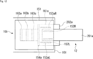
次に、図4乃至図7を参照して、コネクタ105の詳細について説明する。図4は、コネクタ105を斜め下方向から見た斜視図であり、図5は、コネクタ105を斜め上方向から見た斜視図である。図6は、コネクタ105を下面(基板101に装着される装着面)側から見た図であり、図7は、コネクタ105の後面(伝送ケーブル12が挿入される挿入面)側から見た図である。
Next, the details of the
コネクタ105は、本体部151、導体バネ152L、導体バネ152R、導体バネ153aL乃至153cR、及び、導電性ゴム154a乃至154cを備える。導体バネ152L、導体バネ152R、導体バネ153aL乃至153cR、及び、導電性ゴム154a乃至154cは、それぞれ導電性を有している。
The
本体部151は、表面が導電性を有する略直方体の部材(例えば、金属製の部材、プラスチック等の表面に金属メッキを施した部材等)からなる。本体部151の後面及び下面には、開口部161が形成されている。開口部161の左右方向の幅は、導波管201の幅より少し広く、高さは、伝送ケーブル12の上下方向(導波管201の積層方向)の厚みより少し大きい。
The
また、本体部151の後面には、スロット162a乃至スロット162cが、所定の間隔を空けて上下に並ぶように形成されている。スロット162a乃至スロット162cは、伝送ケーブル12の導電板202a乃至導電板202cより幅及び厚みが少し大きく、開口部161からさらに左右に広がっている。
On the rear surface of the
この開口部161及びスロット162a乃至スロット162cにより、伝送ケーブル12を挿入するための挿入部が構成される。
The
開口部161の天井には、導体バネ152L及び導体バネ152Rが設けられている。導体バネ152Lと導体バネ152Rは、それぞれ前後方向に延びており、所定の間隔を空けて左右に並ぶように配置されている。
A
また、スロット162aの天井には、導体バネ153aL及び導体バネ153aRが設けられている。具体的には、導体バネ153aLは、スロット162aの左側の溝の天井に、前後方向に延びるように設けられている。導体バネ153aRは、スロット162aの右側の溝の天井に、導体バネ153aLと略左右対称の位置に設けられている。
A conductor spring 153aL and a conductor spring 153aR are provided on the ceiling of the
さらに、導体バネ153bL及び導体バネ153bRが、スロット162bの天井において、導体バネ153aL及び導体バネ153aRと上下方向に重なる位置に設けられている。また、導体バネ153cL及び導体バネ153cRが、スロット162cの天井において、導体バネ153aL及び導体バネ153aRと上下方向に重なる位置に設けられている。
Furthermore, the conductor springs 153bL and the conductor springs 153bR are provided at positions that overlap the conductor springs 153aL and 153aR in the vertical direction on the ceiling of the
また、スロット162a乃至スロット162cの奥には、導電性ゴム154a乃至154cが導電性接着剤により接合されている。導電性ゴム154a乃至154cは、左右に延びる板状で、導電性を有している。
In addition,
さらに、本体部151には、導波路163a乃至導波路163cが形成されている。導波路163a乃至導波路163cは、断面が左右に細長い矩形の孔が、L字型に折れ曲がった形状を有しており、それぞれ本体部151の挿入部と下面とを接続する。
Further, the
なお、以下、基板101に実装される面であるコネクタ105の本体部151の下面を実装面とも称する。なお、以下、基板101の各部品(例えば、コネクタ105等)が実装される面も実装面と称する。
Hereinafter, the lower surface of the
導波路163aは、導波管201a用の導波路である。導波路163aの一方の開口は、導波管201aの断面より少し大きい矩形であり、開口部161の奥においてスロット162aの上に形成されている。導波路163aの他方の開口は、本体部151の下面において、基板101のスロット121aに対応する位置に形成されている。
The
導波路163bは、導波管201b用の導波路である。導波路163bの一方の開口は、導波管201bの断面より少し大きい矩形であり、開口部161の奥においてスロット162aとスロット162bの間に形成されている。導波路163bの他方の開口は、本体部151の下面において、基板101のスロット121bに対応する位置に形成されている。
The
導波路163cは、導波管201c用の導波路である。導波路163cの一方の開口は、導波管201cの断面より少し大きい矩形であり、開口部161の奥においてスロット162bとスロット162cの間に形成されている。導波路163cの他方の開口は、本体部151の下面において、基板101のスロット121cに対応する位置に形成されている。
The
従って、導波路163a乃至導波路163cの後面側の開口は、所定の間隔を空けて上下に並ぶように配置されている。導波路163a乃至導波路163cの下面側の開口は、前後方向(伝送ケーブル12の挿入方向)に並ぶように配置されている。
Therefore, the openings on the rear surface side of the
なお、導波管201d用の導波路は、開口部161の一部により構成される。
Note that the waveguide for the
また、導波路163a乃至導波路163c、及び、導波管201d用の導波路に対して、例えば、寸法を調整したり、又は、特定の誘電率の誘電体を充填したりする等により、各導波路間の整合性をとるように特性インピーダンスが調整される。
Further, the
なお、以下、導体バネ152Lと導体バネ152Rを個々に区別する必要がない場合、単に導体バネ152と称する。また、以下、導体バネ153aL乃至導体バネ153cRを個々に区別する必要がない場合、単に導体バネ153と称する。
Hereinafter, when there is no need to distinguish between the
次に、図8乃至図11を参照して、伝送ケーブル12の詳細について説明する。図8は、伝送ケーブル12の電子機器11a側の端部付近の斜視図であり、図9は、伝送ケーブル12の電子機器11a側の端部付近の平面図であり、図10は、伝送ケーブル12の電子機器11a側の端部付近の左側面図であり、図11は、伝送ケーブル12の電子機器11a側の端部付近の正面図である。
Next, details of the
伝送ケーブル12においては、導波管201a乃至導波管201dの端部が揃えられ、幅の広い方の側面が向き合うように縦方向に並べられている(積層されている)。導波管201aと導波管201bの間には、導電板202aが挿入され、導波管201aと導波管201bの対向する面が、導電性の接着材により導電板202aの互いに反対側の面に接合されている。導波管201bと導波管201cの間には、導電板202bが挿入され、導波管201bと導波管201cの対向する面が、導電性の接着材により導電板202bの互いに反対側の面に接合されている。導波管201cと導波管201dの間には、導電板202cが挿入され、導波管201cと導波管201dの対向する面が、導電性の接着材により導電板202cの互いに反対側の面に接合されている。
In the
また、導電板202の幅は、導波管201の導電板202に接合されている面の幅より広く、導電板202の先端は、導波管201の先端から突出している。 Further, the width of the conductive plate 202 is wider than the width of the surface of the waveguide 201 joined to the conductive plate 202, and the tip of the conductive plate 202 protrudes from the tip of the waveguide 201.
なお、伝送ケーブル12の電子機器11b側も、電子機器11a側と同様の構成を有しており、その説明は省略する。
Note that the
このように、複数の導波管201の端部が導電板202により束ねられ、ハーネス化される。 As described above, the ends of the plurality of waveguides 201 are bundled by the conductive plate 202 to form a harness.
図12乃至図14は、コネクタ105に伝送ケーブル12を挿入した状態を示している。具体的には、図12は、コネクタ105の各部と伝送ケーブル12の位置関係を模式的に示している。図13は、コネクタ105に伝送ケーブル12を挿入した状態を、コネクタ105の後ろ側(挿入面側)から見た場合の模式図である。図14は、コネクタ105に伝送ケーブル12を挿入した状態における伝送ケーブル12の左上付近を模式的に示している。
12 to 14 show a state in which the
伝送ケーブル12をコネクタ105の挿入部(開口部161及びスロット162a乃至スロット162c)に挿入すると、導電板202a乃至導電板202cが、スロット162a乃至スロット162cに挿入される。また、導電板202a乃至導電板202cの先端が、スロット162a乃至スロット162cの奥の導電性ゴム154a乃至導電性ゴム154cに当接し、密着する。これにより、各導電板202とコネクタ105の間の隙間を塞ぎ、電磁波漏れを抑制することができる。また、各導波管202が、基板101の実装面(コネクタ105の本体部151の実装面)に対して略垂直な方向(上下方向)に並べられる。
When the
そして、開口部161の天井の導体バネ152L及び導体バネ152Rにより、伝送ケーブル12の最も外側に配置されている導波管201aの上面が下方向(各導波管201の側面が対向する方向)に押し付けられる。
Then, the upper surface of the
また、導電板202aが、スロット162aの天井の導体バネ153aL及び導体バネ153aRにより下方向(各導波管201の側面が対向する方向)に押し付けられる。これにより、導電板202aの下面がスロット162aの床面に密着する。同様に、導電板202bが、スロット162bの天井の導体バネ153bL及び導体バネ153bRにより下方向に押し付けられ、導電板202bの下面がスロット162bの床面に密着する。導電板202cが、スロット162cの天井の導体バネ153cL及び導体バネ153cRにより下方向に押し付けられ、導電板202cの下面がスロット162cの床面に密着する。
The
このように、伝送ケーブル12をコネクタ105に挿入すると、導体バネ152及び導体バネ153により、伝送ケーブル12が全体的に下方向に押し付けられ、各導波管201が、直接又は間接的に下方向に押し付けられる。これにより、伝送ケーブル12がコネクタ105の挿入部に固定され、各導波管201の位置が固定される。また、コネクタ105の下面(実装面)に最も近い位置に挿入されている導波管201dの下面が、開口部161の下面の開口を介して、基板101の上面に接触し、密着する。
As described above, when the
ここで、図13に示されるように、伝送ケーブル12をコネクタ105に挿入した状態において、導波管201aとコネクタ105の本体部151との間に隙間ができる。この隙間は、導体バネ152L及び導体バネ152Rにより三分割される。この隙間の導体バネ152Lから導電板202aまでの幅をW1、導体バネ152Lと導体バネ152Rとの間の幅をW2、導体バネ152Rから導電板202aまでの幅をW3とする。また、幅W1乃至幅W3のうち最も長い幅をWmaxとする。
Here, as shown in FIG. 13, a gap is formed between the
そうすると、導波管201aの基本モード(TE10)のカットオフ周波数fcは、幅Wmax、誘電率εγ、及び、光速cに基づいて、次式(1)により求められる。
Then, the cutoff frequency fc of the fundamental mode (TE10) of the
![]()
![]()
従って、幅Wmaxが短くなるほど、カットオフ周波数fcが高くなり、低い周波数の信号が隙間から漏れにくくなる。 Therefore, the shorter the width Wmax, the higher the cutoff frequency fc, and the lower frequency signals are less likely to leak from the gap.
なお、幅Wmaxは、導波管201aにより伝送するミリ波信号の波長の1/2以下となるように設計することが望ましい。また、導波管201aとコネクタ105の本体部151との間の隙間の厚み(導波管201aと本体部151との間の距離)は、幅Wmaxの1/2以下となるように設計することが望ましい。さらに、導体バネ152のミリ波信号の伝送方向(前後方向)の長さは、導波管201aにより伝送するミリ波信号の波長の1/2以上となるように設計することが望ましい。また、導体バネ152の厚みは、導波管201aの導体層の厚みより大きい方が好ましい。
The width Wmax is desirably designed to be equal to or less than ½ of the wavelength of the millimeter wave signal transmitted through the
導波管201b乃至導波管201dとコネクタ105の本体部151との間の隙間は、導波管201aと本体部151との間の隙間より狭いため、導波管201aと本体部151との間の隙間が上記の条件を満たしていれば、それほど考慮する必要はない。なお、各導体バネ153のミリ波信号の伝送方向(前後方向)の長さは、各導波管201により伝送するミリ波信号の波長の1/2以上となるように設計することが望ましい。
Since the gap between the
次に、図15を参照して、通信モジュール21aと伝送ケーブル12との間の信号の流れについて説明する。図15は、図3の点線の枠A1で囲まれた部分の断面を模式的に示している。
Next, with reference to FIG. 15, the flow of signals between the
基板101の上面及び下面には、導体層122a及び導体層122eが形成されている。また、基板101の内部にも導体層122b乃至導体層122dが形成されており、導体層122b乃至導体層122dにより、基板101が第1層101A乃至第4層101Dに分かれる。導体層122a乃至導体層122eは、例えば、銅箔からなる。
また、コネクタ105の導波路163a乃至導波路163cの開口部に対応する位置において、導体層122aに開口部が設けられており、この開口部がスロット121a乃至スロット121cを構成する。さらに、コネクタ105の開口部161の奥付近において、導体層122aに開口部が設けられており、この開口部がスロット121dを構成する。
The
また、導体層122aと導体層122bは、複数本のビア123aにより連結されている。導体層122bと導体層122cは、複数本のビア123bにより連結されている。導体層122cと導体層122dは、複数本のビア123cにより連結されている。導体層122dと導体層122eは、複数本のビア123dにより連結されている。
The
そして、導体層122a及び導体層122b、並びに、ビア123aで囲まれる領域により、導波路124aが形成されている。導波路124aは、基板101の第1層101Aにおいて、スロット121aと送信チップ102aとの間を接続する。送信チップ102aから出力されたミリ波信号は、基板101の導波路124a、及び、コネクタ105の導波路163aを介して、導波管201aに挿入される。
A
また、導体層122b及び導体層122c、並びに、ビア123a及びビア123bで囲まれる領域により、導波路124bが形成されている。導波路124bは、基板101の第1層101Aを貫通し、第2層101Bにおいて、スロット121bと受信チップ103aとの間を接続する。導波管201bにより伝送されてきたミリ波信号は、コネクタ105の導波路163b、及び、基板101の導波路124bを介して、受信チップ103aに供給される。
The
さらに、導体層122c及び導体層122d、並びに、ビア123a乃至ビア123cで囲まれる領域により、導波路124cが形成されている。導波路124cは、基板101の第1層101A及び第2層101Bを貫通し、第3層101Cにおいて、スロット121cと送信チップ102bとの間を接続する。送信チップ102bから出力されたミリ波信号は、基板101の導波路124c、及び、コネクタ105の導波路163cを介して、導波管201cに挿入される。
Further, a
また、導体層122d及び導体層122e、並びに、ビア123a乃至ビア123dで囲まれる領域により、導波路124dが形成されている。導波路124dは、基板101の第1層101A乃至第3層101Cを貫通し、第4層101Dにおいて、スロット121dと受信チップ103bとの間を接続する。導波管201dにより伝送されてきたミリ波信号は、コネクタ105の本体部151の開口部161の一部により構成される導波路、及び、基板101の導波路124dを介して、受信チップ103bに供給される。
A
以上のように、導波管201a乃至導波管201dを縦方向に並べることにより、コネクタ105及び通信モジュール21aの幅を小さくすることができる。より具体的には、コネクタ105及び通信モジュール21の幅を伝送ケーブル12の幅と略同等のサイズにすることができる。その結果、複数の導波管を用いる機器や部品のサイズを小さくすることができる。
As described above, the widths of the
また、送信チップ102a及び受信チップ103aと、送信チップ102b及び受信チップ103bとを、基板101の両面に配置することにより、通信モジュール21(基板101)の面積を小さくすることができる。
Further, by arranging the
さらに、上述した特許文献1に記載の技術では、コネクタ部と導波管とが一体化されていた。そのため、例えば、コネクタ部と導波管を全てフレキシブルプリント基板のプロセスで製作する必要があるとともに、1枚のパネルから製作できる数が少なくなり、コストが高くなる可能性がある。また、コネクタ部及び導波管の一方に不良や故障が発生しても、一方のみを修理することは困難であり、全て取り換える必要が生じる。 Furthermore, in the technique described in Patent Document 1 described above, the connector portion and the waveguide are integrated. For this reason, for example, it is necessary to manufacture all of the connector portion and the waveguide by the process of the flexible printed circuit board, and the number that can be manufactured from one panel is reduced, which may increase the cost. Further, even if one of the connector portion and the waveguide is defective or failed, it is difficult to repair only one of them, and it is necessary to replace all of them.
これに対して、通信システム10では、伝送ケーブル12が通信モジュール21のコネクタ105に着脱可能であり、伝送ケーブル12とコネクタ105(通信モジュール21)とをそれぞれ最適なプロセスで製造することができ、コストを削減することができる。また、伝送ケーブル12とコネクタ105の一方に不良や故障が発生したときに、一方のみを修理又は交換することができ、必要なコストを削減することができる。
On the other hand, in the
さらに、導波路124a乃至導波路124dの一部の区間を基板101内で上下方向に積層することにより、導波路124a乃至導波路124dを、ビア123a乃至ビア123dで分離する部分を少なくすることができる。これにより、導波路124a乃至導波路124d間の信号の干渉を抑制し、各導波路により伝送される信号のアイソレーションを向上させることができる。
Further, by stacking a part of the
また、送信チップ102aと受信チップ103aとの間がシールド104aにより分離されているため、チップ間の信号の干渉を抑制し、各信号のアイソレーションを向上させることができる。同様に、送信チップ102bと受信チップ103bとの間がシールド104bにより分離されているため、チップ間の信号の干渉を抑制し、各信号のアイソレーションを向上させることができる。
Further, since the
さらに、導体バネ152、導体バネ153、及び、導電性ゴム154a乃至154cにより、伝送ケーブル12とコネクタ105との間の隙間を小さくすることにより、隙間からの電磁波漏れが抑制され、不要輻射やクロストーク等の発生が抑制される。
Further, by reducing the gap between the
<2.第2の実施の形態>
次に、図16乃至図18を参照して、本技術の第2の実施の形態について説明する。
<2. Second Embodiment>
Next, a second embodiment of the present technology will be described with reference to FIGS. 16 to 18.
図16及び図17は、伝送ケーブル12を接続した状態の通信モジュール301aを模式的に示している。図16は、通信モジュール301aを上方から見た模式図であり、図17は、通信モジュール301aを側方から見た模式図である。なお、図中、図2及び図3と対応する部分には、同じ符号を付してある。図18は、図17の点線の枠A2で囲まれる部分の断面を模式的に示している。なお、図中、図15と対応する部分には、同じ符号を付してある。
16 and 17 schematically show the
本技術の第2の実施の形態は、第1の実施の形態と比較して、通信モジュール21a及び通信モジュール21bの代わりに、通信モジュール301a及び通信モジュール301b(不図示)が設けられる点が異なる。
The second embodiment of the present technology is different from the first embodiment in that a
通信モジュール301aは、通信モジュール21aと比較して、基板101、並びに、シールド104a及びシールド104bの代わりに、基板321、並びに、シールド322a及びシールド322bが設けられている点が異なる。また、通信モジュール301aは、通信モジュール21aと比較して、送信チップ102aと受信チップ103a、及び、送信チップ102bと受信チップ103bが、左右に並べられている点が異なる。
The
具体的には、基板321の上面には、受信チップ103aと送信チップ102aが、基板101の前端から所定の距離だけ離れた位置において左右に並ぶように実装されている。また、基板321の上面には、送信チップ102a及び受信チップ103aの後方、かつ、送信チップ102a及び受信チップ103aから所定の距離だけ離れた位置において、コネクタ105が実装されている。
Specifically, the
基板321の下面の略前端には、コネクタ106が実装されている。また、コネクタ106の後方には、送信チップ102bと受信チップ103b(図18)が左右に並ぶように配置されている。受信チップ103aと送信チップ102bは、基板101を挟んで略同じ位置に実装されており、送信チップ102aと受信チップ103bは、基板101を挟んで略同じ位置に実装されている。
A
また、基板321の上面であって、コネクタ105が実装されている位置には、左右に延びるスロット341a乃至スロット341dが、前後方向に並ぶように形成されている。
Further,
シールド322aは、送信チップ102a及び受信チップ103aの周囲を覆うとともに、送信チップ102aと受信チップ103aの間を分離している。シールド322bは、送信チップ102b及び受信チップ103bの周囲を覆うとともに、送信チップ102bと受信チップ103bの間を分離している。
The
図18に示されるように、基板321の上面及び下面には、導体層342a及び導体層342eが形成されている。また、基板321の内部にも導体層342b乃至導体層342dが形成されており、導体層342b乃至導体層342dにより、基板321が第1層321A乃至第4層321Dに分かれる。
As shown in FIG. 18, a
また、コネクタ105の導波路163a乃至導波路163cの開口部に対応する位置において、導体層342aに開口部が設けられており、この開口部がスロット341a乃至スロット341cを構成する。さらに、コネクタ105の開口部161の奥付近において、導体層342aに開口部が設けられており、この開口部がスロット341dを構成する。
In addition, openings are provided in the
また、導体層342aと導体層342bは、複数本のビア343aにより連結されている。導体層342bと導体層342cは、複数本のビア343bにより連結されている。導体層342cと導体層342dは、複数本のビア343cにより連結されている。導体層342dと導体層342eは、複数本のビア343dにより連結されている。
The
そして、導体層342a及び導体層342b、並びに、ビア343aで囲まれる領域により、導波路344aが形成されている。導波路344aは、基板321の第1層321Aにおいて、スロット341aと送信チップ102aとの間を接続する。送信チップ102aから出力されたミリ波信号は、基板321の導波路344a、及び、コネクタ105の導波路163aを介して、導波管201aに挿入される。
A
また、導体層342b及び導体層342c、並びに、ビア343a及びビア343bで囲まれる領域により、導波路344bが形成されている。導波路344bは、基板321の第1層321Aを貫通し、第2層321Bにおいて、スロット341bと受信チップ103aとの間を接続する。導波管201bにより伝送されてきたミリ波信号は、コネクタ105の導波路163b、及び、基板321の導波路344bを介して、受信チップ103aに供給される。
A
さらに、導体層342c及び導体層342d、並びに、ビア343a乃至ビア343cで囲まれる領域により、導波路344cが形成されている。導波路344cは、基板321の第1層321A及び第2層321Bを貫通し、第3層321Cにおいて、スロット341cと送信チップ102との間を接続する。送信チップ102bから出力されたミリ波信号は、基板321の導波路344c、及び、コネクタ105の導波路163cを介して、導波管201cに挿入される。
Further, a
また、導体層342d及び導体層342e、並びに、ビア343a乃至ビア343dで囲まれる領域により、導波路344dが形成されている。導波路344dは、基板321の第1層321A乃至第3層321Cを貫通し、第4層321Dにおいて、スロット341dと受信チップ103bとの間を接続する。導波管201dにより伝送されてきたミリ波信号は、コネクタ105の本体部151の開口部161の一部により構成される導波路、及び、基板321の導波路344dを介して、受信チップ103bに供給される。
A
なお、通信モジュール301bの構成は、通信モジュール301aと同様であり、その説明は省略する。
The configuration of the communication module 301b is the same as that of the
以上のように、各チップを伝送ケーブル12の挿入方向に対して垂直な方向に並べることも可能である。
As described above, the chips can be arranged in a direction perpendicular to the insertion direction of the
<3.第3の実施の形態>
次に、図19乃至図21を参照して、本技術の第3の実施の形態について説明する。
<3. Third Embodiment>
Next, a third embodiment of the present technology will be described with reference to FIGS.
図19及び図20は、伝送ケーブル401a及び伝送ケーブル401bを接続した状態の通信モジュール402aを模式的に示している。図19は、通信モジュール402aを上方から見た模式図であり、図20は、通信モジュール402aを側方から見た模式図である。なお、図中、図2及び図3と対応する部分には、同じ符号を付してある。図21は、図20の点線の枠A3で囲まれる部分の断面を模式的に示している。なお、図中、図15と対応する部分には、同じ符号を付してある。
19 and 20 schematically show the
本技術の第3の実施の形態は、第1の実施の形態と比較して、伝送ケーブル12の代わりに、伝送ケーブル401a及び伝送ケーブル401bが設けられ、通信モジュール21a及び通信モジュール21bの代わりに、通信モジュール402a及び通信モジュール402b(不図示)が設けられる点が異なる。
Compared with the first embodiment, the third embodiment of the present technology includes a
伝送ケーブル401a及び伝送ケーブル401bは、伝送ケーブル12と比較して、導波管の積層数が異なる。すなわち、伝送ケーブル12の積層数が4であるのに対し、伝送ケーブル401a及び伝送ケーブル401bの積層数は2である。
The
伝送ケーブル401aにおいては、導波管201aと導波管201bの間に導電板202aが挿入され、導波管201a及び導波管201bと導電板202aとが、導電性の接着材により接合されている。
In the
伝送ケーブル401bにおいては、導波管201cと導波管201dの間に導電板202bが挿入され、導波管201c及び導波管201dと導電板202bとが、導電性の接着材により接合されている。
In the
通信モジュール402aは、通信モジュール21aと比較して、基板101の代わりに、基板421が設けられ、コネクタ105の代わりに、コネクタ423a及びコネクタ423bが設けられている点が異なる。通信モジュール402aは、通信モジュール21aと比較して、コネクタ423a及びコネクタ423bが、基板421の両面に実装されている点が大きく異なる。
The
基板421の上面には、受信チップ103a、送信チップ102a、コネクタ423aが、基板101の前端から所定の距離だけ離れた位置から前後方向に並ぶように実装されている。基板101の下面には、コネクタ106、送信チップ102b、受信チップ103b、コネクタ423bが、基板101の略前端付近から前後方向に並ぶように実装されている。受信チップ103aと送信チップ102bは、基板421を挟んで略同じ位置に実装されており、送信チップ102aと受信チップ103bは、基板421を挟んで略同じ位置に実装されている。また、コネクタ423aとコネクタ423bとは、基板421を挟んで略同じ位置に実装されている。
On the upper surface of the
また、基板421の上面であって、コネクタ423aが実装されている位置には、左右に延びるスロット441a及びスロット441bが、前後方向に並ぶように形成されている。また、基板421の下面のスロット441a及びスロット441bに対応する位置に、スロット441d及びスロット441cがそれぞれ形成されている。
Further,
コネクタ423aは、図4乃至図7のコネクタ105と比較して、スロット及び導波路の数が異なる。すなわち、コネクタ423aに着脱される伝送ケーブル401aの導波管及び導電板の数は、コネクタ105に挿入される伝送ケーブル12の導波管及び導電板の数より少ない。従って、コネクタ423aの本体部461aは、コネクタ105の本体部151と比較して、スロットの数が3つから1つに削減され、L字型の導波路の数が3つから1つに削減される。従って、コネクタ423aは、コネクタ105より高さが低くなり、奥行き方向(前後方向)が短くなる。
The
なお、コネクタ423aにおいても、コネクタ105の導体バネ152L及び導体バネ152Rと同様の導体バネ462aL(不図示)及び導体バネ462aRが、導体バネ152L及び導体バネ152Rと同様の位置に設けられる。また、コネクタ105の導体バネ153aL及び導体バネ153aRと同様の導体バネ463aL(不図示)及び導体バネ463aR(不図示)が、導体バネ153aL及び導体バネ153aRと同様の位置に設けられる。さらに、コネクタ105の導電性ゴム154cと同様の導電性ゴム464a(図21)が、導電性ゴム154cと同様の位置に設けられる。
Also in the
コネクタ423bは、コネクタ423aと同様の構成を有しており、その説明は省略する。
The
図21に示されるように、基板421の上面及び下面には、導体層442a及び導体層442eが形成されている。また、基板421の内部にも導体層442b乃至導体層442dが形成されており、導体層442b乃至導体層442dにより、基板421が第1層421A乃至第4層421Dに分かれる。
As shown in FIG. 21, a
また、コネクタ423aの導波路471aの開口部に対する位置において、導体層442aに開口部が設けられており、この開口部がスロット441aを構成する。さらに、コネクタ423aの開口部の奥付近において、導体層442aに開口部が設けられており、この開口部がスロット441bを構成する。
In addition, an opening is provided in the
また、コネクタ423bの導波路471bの開口部に対する位置において、導体層442eに開口部が設けられており、この開口部がスロット441dを構成する。さらに、コネクタ423bの開口部の奥付近において、導体層442eに開口部が設けられており、この開口部がスロット441cを構成する。
In addition, an opening is provided in the
また、導体層442aと導体層442bは、複数本のビア443aにより連結されている。導体層442bと導体層442cは、複数本のビア443bにより連結されている。導体層442cと導体層442dは、複数本のビア443cにより連結されている。導体層442dと導体層442eは、複数本のビア443dにより連結されている。
The
そして、導体層442a及び導体層442b、並びに、ビア443aで囲まれる領域により、導波路444aが形成されている。導波路444aは、基板421の第1層421Aにおいて、スロット441aと送信チップ102aとの間を接続する。送信チップ102aから出力されたミリ波信号は、基板421の導波路444a、及び、コネクタ423aの導波路471aを介して、導波管201aに挿入される。
A
また、導体層442b及び導体層442c、並びに、ビア443a及びビア443bで囲まれる領域により、導波路444bが形成されている。導波路444bは、基板421の第1層421Aを貫通し、第2層421Bにおいて、スロット441bと受信チップ103aとの間を接続する。導波管201bにより伝送されてきたミリ波信号は、コネクタ423aの本体部461aの開口部の一部により構成される導波路、及び、基板421の導波路444bを介して、受信チップ103aに供給される。
In addition, a
さらに、導体層442c及び導体層442d、並びに、ビア443c及びビア443dで囲まれる領域により、導波路444cが形成されている。導波路444cは、基板421の第4層421Dを貫通し、第3層421Cにおいて、スロット441cと送信チップ102bとの間を接続する。送信チップ102bから出力されたミリ波信号は、基板421の導波路444c、及び、コネクタ423bの本体部461bの開口部の一部により構成される導波路を介して、導波管201cに挿入される。
Further, a
また、導体層442d及び導体層442e、並びに、ビア443dで囲まれる領域により、導波路444dが形成されている。導波路444dは、基板421の第4層421Dにおいて、スロット441dと受信チップ103bとの間を接続する。導波管201dにより伝送されてきたミリ波信号は、コネクタ423bの導波路471b、及び、基板421の導波路444dを介して、受信チップ103aに供給される。
A
なお、コネクタ423aの導波路471a及び導波管201b用の導波路、並びに、コネクタ423bの導波路471b及び導波管201c用の導波路に対して、例えば、寸法を調整したり、又は、特定の誘電率の誘電体を充填したりする等により、各導波路間の整合性をとるように特性インピーダンスが調整される。
For example, the dimensions of the
なお、通信モジュール402bの構成は、通信モジュール402aと同様であり、その説明は省略する。
The configuration of the
以上のように、伝送ケーブルを2つに分け、通信モジュールの基板の両面に、伝送ケーブル用のコネクタを設けることも可能である。 As described above, it is also possible to divide the transmission cable into two and provide transmission cable connectors on both sides of the communication module substrate.
<4.第4の実施の形態>
次に、図22乃至図24を参照して、本技術の第4の実施の形態について説明する。
<4. Fourth Embodiment>
Next, a fourth embodiment of the present technology will be described with reference to FIGS.
図22及び図23は、導波管201a乃至導波管201dを通信モジュール501aに接続した状態の通信モジュール501aを模式的に示している。図22は、通信モジュール501aを上方から見た模式図であり、図23は、通信モジュール501aを側方から見た模式図である。なお、図中、図2及び図3と対応する部分には、同じ符号を付してある。図24は、図23の点線の枠A4で囲まれる部分の断面を模式的に示している。なお、図中、図15と対応する部分には、同じ符号を付してある。
22 and 23 schematically show the
本技術の第4の実施の形態は、第1の実施の形態と比較して、通信モジュール21a及び通信モジュール21bの代わりに、通信モジュール501a及び通信モジュール501b(不図示)が設けられ、導波管201a乃至導波管201dが、ハーネス化されずに、そのまま1本ずつ通信モジュール501a及び通信モジュール501bに着脱される点が異なる。
Compared with the first embodiment, the fourth embodiment of the present technology includes a
通信モジュール501aは、通信モジュール21aと比較して、コネクタ105の代わりに、コネクタ521が設けられている点が異なる。また、導波管201がハーネス化されておらず、各導波管201が個別にコネクタ521に挿入される点が異なる。
The
図24に示されるように、コネクタ521の本体部561には、導波路571a乃至導波路571dが形成されている。
As shown in FIG. 24, a
導波路571a乃至導波路571cは、コネクタ105の導波路163a乃至導波路163cと同様に、断面が左右に細長い矩形の孔が、L字型に折れ曲がった形状を有している。
Similarly to the
導波路571aは、導波管201aの挿入部を兼ね、導波管201aが着脱される導波路である。導波路571aの一方の開口は、導波管201aの断面より少し大きい矩形であり、コネクタ521の本体部561の後面(導波管201aが挿入される挿入面)に形成されている。導波路571aの他方の開口は、本体部561の下面において、基板101のスロット121aに対応する位置に形成されている。
The
また、導波路571aには、導体バネ152L及び導体バネ152Rと同様の導体バネ562aL(不図示)及び導体バネ562aRが、導波路163aにおける導体バネ152L及び導体バネ152Rとほぼ同様の位置に設けられている。この導体バネ562aL及び導体バネ562aRにより、導波管201aが下方向(各導波管201の側面が対向する方向)に押し付けられ、導波路571aの床面に密着する。これにより、導波管201aと導波路571aの床面との間の隙間が塞がれるとともに、導波管201aが導波路571a内に固定される。
The
導波路571bは、導波管201bの挿入部を兼ね、導波管201bが着脱される導波路である。導波路571bの一方の開口は、導波路571aの後面側の開口と略同じ形状であり、コネクタ521の本体部561の後面(導波管201bが挿入される挿入面)において、導波路571aの開口より下方向に所定の距離だけ離れた位置に形成されている。導波路571bの他方の開口は、本体部561の下面において、基板101のスロット121bに対応する位置に形成されている。
The waveguide 571b serves as an insertion portion of the
また、導波路571bには、導体バネ562aL及び導体バネ562aRと同様の導体バネ562bL(不図示)及び導体バネ562bRが、導体バネ562aL及び導体バネ562aRと上下方向に略重なる位置に設けられている。この導体バネ562bL及び導体バネ562bRにより、導波管201bが下方向(各導波管201の側面が対向する方向)に押し付けられ、導波路571bの床面に密着する。これにより、導波管201bと導波路571bの床面との間の隙間が塞がれるとともに、導波管201bが導波路571b内に固定される。
In addition, a conductor spring 562bL (not shown) and a conductor spring 562bR similar to the conductor spring 562aL and the conductor spring 562aR are provided in the waveguide 571b at positions that substantially overlap the conductor spring 562aL and the conductor spring 562aR in the vertical direction. . By the conductor springs 562bL and the conductor springs 562bR, the
導波路571cは、導波管201cの挿入部を兼ね、導波管201cが着脱される導波路である。導波路571cの一方の開口は、導波路571aの後面側の開口と略同じ形状であり、コネクタ521の本体部561の後面(導波管201cが挿入される挿入面)において、導波路571bの開口より下方向に所定の距離だけ離れた位置に形成されている。導波路571cの他方の開口は、本体部561の下面において、基板101のスロット121cに対応する位置に形成されている。
The
また、導波路571cには、導体バネ562aL及び導体バネ562aRと同様の導体バネ562cL(不図示)及び導体バネ562cRが、導体バネ562aL及び導体バネ562aRと上下方向に略重なる位置に設けられている。この導体バネ562cL及び導体バネ562cRにより、導波管201cが下方向(各導波管201の側面が対向する方向)に押し付けられ、導波路571cの床面に密着する。これにより、導波管201cと導波路571cの床面との間の隙間が塞がれるとともに、導波管201cが導波路571c内に固定される。
In addition, a conductor spring 562cL (not shown) and a conductor spring 562cR similar to the conductor spring 562aL and the conductor spring 562aR are provided in the
導波路571dは、導波管201dの挿入部を兼ね、導波管201dが着脱される導波路である。導波路571dは、コネクタ521の本体部561の後面及び下面に形成されている。導波路571dの後面側の開口は、導波路571aの後面側の開口と略同じ形状である。
The
また、導波路571dには、導体バネ562aL及び導体バネ562aRと同様の導体バネ562dL(不図示)及び導体バネ562dRが、導体バネ562aL及び導体バネ562aRと上下方向に略重なる位置に設けられている。この導体バネ562dL及び導体バネ562dRにより、導波管201dが下方向(各導波管201の側面が対向する方向)に押し付けられ、基板101の実装面に密着する。これにより、導波管201dと基板101の実装面との間の隙間が塞がれるとともに、導波管201dが導波路571d内に固定される。
In addition, a conductor spring 562dL (not shown) and a conductor spring 562dR similar to the conductor spring 562aL and the conductor spring 562aR are provided in the
なお、導体バネ562aL乃至導体バネ562dRの設置位置、厚み、長さ等の条件は、図13を参照して上述したコネクタ105の導体バネ152L及び導体バネ152Rの条件と同様である。
The conditions such as the installation position, thickness, and length of the conductor springs 562aL to 562dR are the same as the conditions of the
そして、図24に示されるように、送信チップ102aから出力されたミリ波信号は、基板101の導波路124a、及び、コネクタ521の導波路571aを介して、導波管201aに挿入される。
24, the millimeter wave signal output from the
導波管201bにより伝送されてきたミリ波信号は、コネクタ521の導波路571b、及び、基板101の導波路124bを介して、受信チップ103aに供給される。
The millimeter wave signal transmitted through the
送信チップ102bから出力されたミリ波信号は、基板101の導波路124c、及び、コネクタ521の導波路571cを介して、導波管201cに挿入される。
The millimeter wave signal output from the
導波管201dにより伝送されてきたミリ波信号は、コネクタ521の導波路571d、及び、基板101の導波路124dを介して、受信チップ103bに供給される。
The millimeter wave signal transmitted through the
以上のように、通信モジュール501aにおいて、導波管201a乃至導波管201dを個別に上下方向に並べて、コネクタ521に挿入することが可能である。これにより、通信モジュール501aは、上述した通信モジュール21aと同様の効果を奏することができる。また、コネクタ521に導電板に挿入する必要がないため、コネクタ521を通信モジュール21aのコネクタ105より小型化し、通信モジュール501aを通信モジュール21aより小型化することも可能である。
As described above, in the
なお、通信モジュール501bの構成は、通信モジュール501aと同様であり、その説明は省略する。
The configuration of the communication module 501b is the same as that of the
<5.変形例>
以下、上述した本技術の実施の形態の変形例について説明する。
<5. Modification>
Hereinafter, modifications of the above-described embodiment of the present technology will be described.
以上に示した伝送ケーブルの導波管の積層数は、その一例であり、任意に変更することができる。 The number of laminated waveguides of the transmission cable described above is an example, and can be arbitrarily changed.
また、以上の説明では、最も基板に近い位置に配置される導波管の側面を基板の実装面に接触させる例を示したが、他の導波管と同様に、基板の実装面に接触させないようにすることも可能である。なお、基板の実装面に接触させるようにした方が、コネクタの高さを低くすることができる。 In the above description, the example in which the side surface of the waveguide disposed closest to the substrate is brought into contact with the mounting surface of the substrate is shown. However, as with other waveguides, the mounting surface of the substrate is contacted. It is also possible not to let it. Note that the height of the connector can be reduced by bringing it into contact with the mounting surface of the substrate.
さらに、以上の説明では、基板の実装面に対して垂直な方向に導波管を並べてコネクタに挿入する例を示したが、本技術は、例えば、基板の実装面に対して平行な方向に導波管を並べてコネクタに挿入する場合にも適用することができる。すなわち、本技術は、複数の導波管が対向する面が基板の実装面に対して垂直になるように、導波管を並べてコネクタに挿入する場合にも適用することができる。 Furthermore, in the above description, an example in which the waveguides are arranged in a direction perpendicular to the mounting surface of the board and inserted into the connector has been shown. However, the present technology is, for example, in a direction parallel to the mounting surface of the board. The present invention can also be applied to a case where waveguides are aligned and inserted into a connector. In other words, the present technology can also be applied to a case where the waveguides are aligned and inserted into the connector so that the surfaces facing the plurality of waveguides are perpendicular to the mounting surface of the substrate.
また、本技術は、コネクタの面のうち基板の実装面に対して垂直な面以外の面に、伝送ケーブルの挿入部を設ける場合にも適用することができる。例えば、コネクタの上面に挿入部を設けた場合、導波管は基板の実装面に対して垂直にコネクタに挿入され、コネクタ内の各導波管に対応する導波路は、基板の実装面に対して垂直な方向に延びるように配置することが可能である。 The present technology can also be applied to the case where the insertion portion of the transmission cable is provided on a surface other than the surface perpendicular to the mounting surface of the board among the surfaces of the connector. For example, when the insertion portion is provided on the upper surface of the connector, the waveguide is inserted into the connector perpendicular to the mounting surface of the board, and the waveguide corresponding to each waveguide in the connector is placed on the mounting surface of the board. It is possible to arrange them to extend in a direction perpendicular to the direction.
さらに、以上の説明では、導電板の幅が導波管より大きい例を示したが、導電板の幅を導波管の幅以下にすることも可能である。この場合、例えば、コネクタの挿入部において、各導波管に対してスロットが設けられる。 Further, in the above description, an example in which the width of the conductive plate is larger than that of the waveguide has been shown. However, the width of the conductive plate can be made equal to or smaller than the width of the waveguide. In this case, for example, a slot is provided for each waveguide at the insertion portion of the connector.
また、例えば、導電性ゴム以外の導電性を有する部材を用いて、導電板とコネクタの間の隙間を塞ぐようにしてもよい。さらに、導電性ゴムを設けずに、導電板をコネクタに直接接触させるようにすることも可能である。 Further, for example, a member having conductivity other than the conductive rubber may be used to close the gap between the conductive plate and the connector. Furthermore, it is possible to directly contact the conductive plate with the connector without providing conductive rubber.
また、例えば、導電板を導波管の先端から突出させないようにすることも可能である。この場合、上述した導電性ゴム以外の方法により、導波管とコネクタの間の隙間を小さくする対処を行うようにすることが望ましい。 Further, for example, it is possible to prevent the conductive plate from protruding from the tip of the waveguide. In this case, it is desirable to take measures to reduce the gap between the waveguide and the connector by a method other than the conductive rubber described above.
さらに、以上に示した導体バネの数や位置は、その一例であり、任意に変更することができる。なお、図13を参照して上述したように、導体バネにより定まる隙間の幅が狭くするほど、電磁波の漏れを小さくすることができる。 Furthermore, the number and position of the conductor springs described above are merely examples, and can be arbitrarily changed. As described above with reference to FIG. 13, the leakage of electromagnetic waves can be reduced as the width of the gap determined by the conductor spring is reduced.
また、以上の説明では、導体バネにより、導波管及び導電板を下方向に押し付ける例を示したが、上方向に押し付けるようにすることも可能である。この場合、例えば、導体バネが、コネクタの挿入部のスロットの床面等に配置される。 In the above description, the waveguide and the conductive plate are pressed downward by the conductor spring. However, the waveguide and the conductive plate may be pressed upward. In this case, for example, the conductor spring is arranged on the floor surface of the slot of the insertion portion of the connector.
さらに、コネクタでなく、導波管や導電板に導体バネを設けるようにしてもよい。 Furthermore, you may make it provide a conductor spring not in a connector but in a waveguide and a conductive plate.
また、導体バネ以外の導電性を有する固定部材により、導波管や導電板をコネクタに固定するようにしてもよい。 Further, the waveguide and the conductive plate may be fixed to the connector by a fixing member having conductivity other than the conductor spring.
さらに、以上の説明では、伝送ケーブル又は導波管をコネクタに着脱可能な構成を示したが、本技術は、伝送ケーブル及び導波管をコネクタに固定させる場合にも適用することができる。すなわち、伝送ケーブル及び導波管を着脱可能とせず、コネクタに固定させる場合でも、上述したように複数の導波管を幅の広い方の側面が向き合うように並べてコネクタに挿入することにより、コネクタのサイズを小さくすることができる。 Furthermore, in the above description, the configuration in which the transmission cable or the waveguide can be attached to and detached from the connector is shown, but the present technology can also be applied to the case where the transmission cable and the waveguide are fixed to the connector. That is, even when the transmission cable and the waveguide are not detachable and are fixed to the connector, as described above, the plurality of waveguides are inserted in the connector so that the wide side faces face each other. Can be reduced in size.
また、例えば、導波管の断面が正方形に近く、側面の幅に差があまりない場合には、複数の導波管を幅の狭い方の側面が向き合うように並べてコネクタに挿入することも可能である。 For example, if the cross section of the waveguide is close to a square and there is not much difference between the widths of the side surfaces, it is possible to insert a plurality of waveguides side by side with the narrower side facing each other into the connector. It is.
さらに、本技術において、導波管の断面は完全な矩形でなくてもよく、例えば、断面の角が丸みを帯びた略矩形でもよい。また、導波管の断面を矩形以外の形状にすることも可能である。 Furthermore, in the present technology, the cross section of the waveguide may not be a complete rectangle, and may be, for example, a substantially rectangular shape with rounded corners. It is also possible to make the cross section of the waveguide a shape other than a rectangle.
また、以上の説明では、通信モジュールの各チップが送信又は受信の一方のみを行う例を示したが、双方向通信を行うチップを用いることも可能である。この場合、双方向通信を行うチップに対応する導波管及び導波路においては、信号が双方向に伝送される。 In the above description, an example in which each chip of the communication module performs only one of transmission and reception has been described, but a chip that performs bidirectional communication can also be used. In this case, signals are transmitted bidirectionally in the waveguide and waveguide corresponding to the chip performing bidirectional communication.
さらに、以上の説明では、伝送ケーブルの挿入方向又は挿入方向に垂直な方向のいずれかの方向に基板上にチップを並べる例を示したが、両方向にチップを並べるようにすることも可能である。 Furthermore, in the above description, the example in which the chips are arranged on the substrate in either the insertion direction of the transmission cable or the direction perpendicular to the insertion direction has been described. However, it is also possible to arrange the chips in both directions. .
また、以上の説明では、ミリ波帯の信号を送信する例を示したが、本技術は、導波管で伝送可能な信号であれば、ミリ波帯以外の周波数帯の信号を伝送する場合にも適用することができる。 In the above description, an example of transmitting a millimeter-wave band signal has been shown. However, in the present technology, a signal in a frequency band other than the millimeter-wave band is transmitted as long as the signal can be transmitted through a waveguide. It can also be applied to.
なお、本技術の実施の形態は、上述した実施の形態に限定されるものではなく、本技術の要旨を逸脱しない範囲において種々の変更が可能である。 The embodiments of the present technology are not limited to the above-described embodiments, and various modifications can be made without departing from the gist of the present technology.
また、例えば、本技術は以下のような構成も取ることができる。 For example, this technique can also take the following structures.
(1)
複数の導波管が側面を向かい合わせて並べた状態で挿入される挿入部と、
基板に実装される面である実装面と前記挿入部との間を接続し、それぞれ対応する前記導波管により伝送される信号を伝送する複数の導波路と
を備える導波管用コネクタ。
(2)
前記挿入部は、複数の前記導波管を着脱でき、
各前記導波管の側面が対向する方向に直接又は間接的に力を加え、前記導波管を前記挿入部に固定させる固定部材を
さらに備える前記(1)に記載の導波管用コネクタ。
(3)
隣接する前記導波管の対向する面の端部が導電板の互いに反対側の面にそれぞれ接合されることにより複数の前記導波管が束ねられており、
前記固定部材は、最も外側に配置されている前記導波管のうち少なくとも一方の前記導波管の側面を各前記導波管の側面が対向する方向に押すとともに、導電性を有する第1の固定部材を含む
前記(2)に記載の導波管用コネクタ。
(4)
前記導電板の幅は、前記導波管の前記導電板に接合されている面の幅より広く、
前記挿入部は、前記導電板を挿入するためのスロットを備え、
前記固定部材は、前記スロット内において、前記導電板を各前記導波管の側面が対向する方向に押すとともに、導電性を有する第2の固定部材を含む
前記(3)に記載の導波管用コネクタ。
(5)
前記導電板が前記導波管の先端より突出しており、
前記挿入部に複数の前記導波管を挿入したときに前記導電板の先端が当接する位置にある導電性ゴムを
さらに備える前記(4)に記載の導波管用コネクタ。
(6)
前記挿入部は、前記実装面に垂直な面に形成され、
前記実装面に垂直な方向に並ぶように複数の前記導波管が前記挿入部に挿入される
前記(1)乃至(59のいずれかに記載の導波管用コネクタ。
(7)
前記挿入部の前記実装面側が開口されており、
前記実装面に最も近い位置に挿入される前記導波管の側面が、前記挿入部の開口を介して前記基板に接触する
前記(6)に記載の導波管用コネクタ。
(8)
複数の前記導波路の前記実装面側の開口が、前記導波管の挿入方向に並んでいる
前記(6)又は(7)に記載の導波管用コネクタ。
(9)
前記導波管の断面は略矩形であり、
前記挿入部は、前記導波管の幅の広い方の側面を向かい合わせて並べた状態で複数の前記導波管が挿入される
前記(1)乃至(8)のいずれかに記載の導波管用コネクタ。
(10)
基板と、
前記基板の第1の面に実装される第1の導波管用コネクタと
を備え、
前記第1の導波管用コネクタは、
複数の導波管が側面を向かい合わせて並べた状態で挿入される第1の挿入部と、
前記基板の前記第1の面に実装される面である第1の実装面と前記第1の挿入部との間を接続し、それぞれ対応する前記導波管により伝送される信号を伝送する複数の第1の導波路と
を備える通信モジュール。
(11)
前記基板は、
各前記第1の導波路に接続する複数の第2の導波路を
備え、
各前記第2の導波路の少なくとも一部の区間が前記基板内において積層されている
前記(10)に記載の通信モジュール。
(12)
各前記導波管を介して信号の送信及び受信のうち少なくとも一方を行う複数のチップを
さらに備え、
前記第2の導波路は、それぞれ対応する前記チップと前記第1の導波路とを接続する
前記(11)に記載の通信モジュール。
(13)
前記第1の挿入部は、前記実装面に垂直な面に形成され、
前記チップは、前記導波管の前記第1の挿入部への挿入方向及び前記挿入方向に垂直な方向の少なくとも一方向に前記基板上に並べられている
前記(12)に記載の通信モジュール。
(14)
前記チップは、前記基板の両面に実装されている
前記(12)又は(13)に記載の通信モジュール。
(15)
各前記第2の導波路は、前記基板の表面及び内部に形成されている導体層、並びに、隣接する前記導体層間を接続するビアにより形成される
前記(11)乃至(14)のいずれかに記載の通信モジュール。
(16)
前記基板の前記第1の面の反対側の第2の面に実装される第2の導波管用コネクタを
さらに備え、
前記第2の導波管用コネクタは、
複数の前記導波管が側面を向かい合わせて並べた状態で挿入される第2の挿入部と、
前記基板に実装される面である第2の実装面と前記第2の挿入部との間を接続し、それぞれ対応する前記導波管により伝送される信号を伝送する複数の第3の導波路と
を備え、
前記基板は、
各前記第3の導波路に接続する複数の第4の導波路を
備え、
各前記第2の導波路及び各前記第4の導波路の少なくとも一部の区間が前記基板内において積層されている
前記(11)乃至(15)のいずれかに記載の通信モジュール。
(17)
複数の前記導波管を
さらに備える前記(10)乃至(16)のいずれかに記載の通信モジュール。
(18)
複数の導波管と、
複数の導電板と
を備え、
各前記導波管の側面が向かい合うように並べられ、
隣接する前記導波管の対向する面の端部が前記導電板の互いに反対側の面にそれぞれ接合されることにより複数の前記導波管が束ねられている
伝送ケーブル。
(19)
前記導電板の幅は、前記導波管の前記導電板に接合されている面の幅より広く、
前記導電板が、前記導波管の先端より突出している
前記(18)に記載の伝送ケーブル。
(20)
基板と、
前記基板に実装される導波管用コネクタと
を備える通信モジュールと、
前記通信モジュールを介して伝送される信号の処理を行う信号処理部と
を備え、
前記導波管用コネクタは、
複数の導波管が側面を向かい合わせて並べた状態で挿入される挿入部と、
前記基板に実装される面である実装面と前記挿入部との間を接続し、それぞれ対応する前記導波管により伝送される信号を伝送する複数の導波路と
を備える電子機器。
(1)
An insertion portion inserted with a plurality of waveguides arranged side by side facing each other;
A waveguide connector comprising: a plurality of waveguides that connect a mounting surface, which is a surface mounted on a substrate, and the insertion portion, and each transmit a signal transmitted by the corresponding waveguide.
(2)
The insertion section can attach and detach a plurality of the waveguides,
The waveguide connector according to (1), further including a fixing member that applies a force directly or indirectly in a direction in which the side surfaces of each waveguide face each other to fix the waveguide to the insertion portion.
(3)
A plurality of the waveguides are bundled by joining the ends of the opposing surfaces of the adjacent waveguides to the opposite surfaces of the conductive plate, respectively.
The fixing member pushes a side surface of at least one of the waveguides arranged on the outermost side in a direction in which the side surfaces of the waveguides face each other, and has a first conductivity. The waveguide connector according to (2), including a fixing member.
(4)
The width of the conductive plate is wider than the width of the surface joined to the conductive plate of the waveguide,
The insertion portion includes a slot for inserting the conductive plate,
The fixing member includes a second fixing member having conductivity while pushing the conductive plate in a direction in which the side surfaces of the waveguides face each other in the slot. connector.
(5)
The conductive plate protrudes from the end of the waveguide;
The waveguide connector according to (4), further including a conductive rubber at a position where a tip of the conductive plate abuts when a plurality of the waveguides are inserted into the insertion portion.
(6)
The insertion portion is formed on a surface perpendicular to the mounting surface,
The waveguide connector according to any one of (1) to (59), wherein a plurality of the waveguides are inserted into the insertion portion so as to be aligned in a direction perpendicular to the mounting surface.
(7)
The mounting surface side of the insertion part is opened,
The waveguide connector according to (6), wherein a side surface of the waveguide inserted at a position closest to the mounting surface is in contact with the substrate through an opening of the insertion portion.
(8)
The waveguide connector according to (6) or (7), wherein openings on the mounting surface side of the plurality of waveguides are arranged in the insertion direction of the waveguide.
(9)
The waveguide has a substantially rectangular cross section,
The waveguide according to any one of (1) to (8), wherein the insertion section is inserted with a plurality of the waveguides in a state where the wide side surfaces of the waveguide are arranged facing each other. Pipe connector.
(10)
A substrate,
A first waveguide connector mounted on the first surface of the substrate;
The first waveguide connector includes:
A first insertion portion inserted with a plurality of waveguides arranged side by side facing each other;
A plurality of signals are transmitted between the first mounting surface, which is a surface mounted on the first surface of the substrate, and the first insertion portion, and signals transmitted by the corresponding waveguides. A first communication waveguide.
(11)
The substrate is
A plurality of second waveguides connected to each of the first waveguides;
The communication module according to (10), wherein at least some sections of each of the second waveguides are stacked in the substrate.
(12)
A plurality of chips that perform at least one of signal transmission and reception through each of the waveguides;
The communication module according to (11), wherein each of the second waveguides connects the corresponding chip and the first waveguide.
(13)
The first insertion portion is formed on a surface perpendicular to the mounting surface,
The communication module according to (12), wherein the chips are arranged on the substrate in at least one of an insertion direction of the waveguide into the first insertion portion and a direction perpendicular to the insertion direction.
(14)
The communication module according to (12) or (13), wherein the chip is mounted on both surfaces of the substrate.
(15)
Each of the second waveguides is formed by a conductor layer formed on the surface and inside of the substrate, and a via connecting the adjacent conductor layers. Any one of (11) to (14) The communication module described.
(16)
A second waveguide connector mounted on a second surface of the substrate opposite to the first surface;
The second waveguide connector is
A plurality of waveguides inserted in a state where the side surfaces face each other;
A plurality of third waveguides that connect between the second mounting surface, which is a surface mounted on the substrate, and the second insertion portion, and transmit signals transmitted by the corresponding waveguides, respectively. And
The substrate is
A plurality of fourth waveguides connected to each of the third waveguides;
The communication module according to any one of (11) to (15), wherein at least a part of each of the second waveguides and each of the fourth waveguides is stacked in the substrate.
(17)
The communication module according to any one of (10) to (16), further including a plurality of the waveguides.
(18)
A plurality of waveguides;
A plurality of conductive plates, and
The waveguides are arranged so that the sides of the waveguides face each other,
A plurality of the waveguides are bundled by joining end portions of opposing surfaces of the adjacent waveguides to opposite surfaces of the conductive plate, respectively.
(19)
The width of the conductive plate is wider than the width of the surface joined to the conductive plate of the waveguide,
The transmission cable according to (18), wherein the conductive plate protrudes from a distal end of the waveguide.
(20)
A substrate,
A communication module comprising: a waveguide connector mounted on the substrate;
A signal processing unit for processing a signal transmitted via the communication module,
The waveguide connector is
An insertion portion inserted with a plurality of waveguides arranged side by side facing each other;
An electronic apparatus comprising: a plurality of waveguides that connect a mounting surface, which is a surface mounted on the substrate, and the insertion portion, and transmit signals transmitted through the corresponding waveguides.
10 通信システム, 11a,11b 電子機器, 12 伝送ケーブル, 21a,21b 通信モジュール, 22a,22b 信号処理部, 101 基板, 102a,102b 送信チップ, 103a,103b 受信チップ, 104a,104b シールド, 105,106 コネクタ, 121a乃至121d スロット, 122a乃至122e 導体層, 123a乃至123d ビア, 124a乃至124d 導波路, 151 本体部, 152L,152R,153aL乃至153cR 導体バネ, 154a乃至154c 導電性ゴム, 161 開口部, 162a乃至162c スロット, 163a乃至163c 導波路, 201a乃至201d 導波管, 202a乃至202c 導電板, 301a,301b 通信モジュール, 321 基板, 322a,322b シールド, 341a乃至341c スロット, 342a乃至342e 導体層, 343a乃至343d ビア, 344a乃至344d 導波路, 401a,401b 伝送ケーブル, 402a,402b 通信モジュール, 421 基板, 422a,422b シールド, 423a,423b コネクタ, 441a乃至441d スロット, 442a乃至442e 導体層, 443a乃至443d ビア, 444a乃至444d 導波路, 461a,461b 本体部, 462aL乃至462bR 導体バネ, 463aL乃至導体バネ463bR 導体バネ, 464a,464b 導電性ゴム, 471a,471b 導波路, 501a,501b 通信モジュール, 521 コネクタ, 561 本体部, 562aL乃至562dR 導体バネ, 571a乃至571d 導波路 10 communication system, 11a, 11b electronic device, 12 transmission cable, 21a, 21b communication module, 22a, 22b signal processing unit, 101 substrate, 102a, 102b transmission chip, 103a, 103b reception chip, 104a, 104b shield, 105, 106 Connector, 121a to 121d slot, 122a to 122e conductor layer, 123a to 123d via, 124a to 124d waveguide, 151 body, 152L, 152R, 153aL to 153cR conductor spring, 154a to 154c conductive rubber, 161 opening, 162a To 162c slot, 163a to 163c waveguide, 201a to 201d waveguide, 202a to 202c conductive plate, 301a, 301b communication module , 321 substrate, 322a, 322b shield, 341a to 341c slot, 342a to 342e conductor layer, 343a to 343d via, 344a to 344d waveguide, 401a, 401b transmission cable, 402a, 402b communication module, 421 substrate, 422a, 422b shield, 423a, 423b connector, 441a to 441d slot, 442a to 442e conductor layer, 443a to 443d via, 444a to 444d waveguide, 461a, 461b main body, 462aL to 462bR conductor spring, 463aR to conductor spring 463aR to conductor spring 463aL 464a, 464b conductive rubber, 471a, 471b waveguide, 501a, 501b communication module, 521 connector, 561 body, 562aL to 562dR conductor spring, 571a to 571d waveguide
Claims (20)
基板に実装される面である実装面と前記挿入部との間を接続し、それぞれ対応する前記導波管により伝送される信号を伝送する複数の導波路と
を備える導波管用コネクタ。 An insertion portion inserted with a plurality of waveguides arranged side by side facing each other;
A waveguide connector comprising: a plurality of waveguides that connect a mounting surface, which is a surface mounted on a substrate, and the insertion portion, and each transmit a signal transmitted by the corresponding waveguide.
各前記導波管の側面が対向する方向に直接又は間接的に力を加え、前記導波管を前記挿入部に固定させる固定部材を
さらに備える請求項1に記載の導波管用コネクタ。 The insertion section can attach and detach a plurality of the waveguides,
The waveguide connector according to claim 1, further comprising a fixing member that applies a force directly or indirectly in a direction in which the side surfaces of each waveguide face each other to fix the waveguide to the insertion portion.
前記固定部材は、最も外側に配置されている前記導波管のうち少なくとも一方の前記導波管の側面を各前記導波管の側面が対向する方向に押すとともに、導電性を有する第1の固定部材を含む
請求項2に記載の導波管用コネクタ。 A plurality of the waveguides are bundled by joining the ends of the opposing surfaces of the adjacent waveguides to the opposite surfaces of the conductive plate, respectively.
The fixing member pushes a side surface of at least one of the waveguides arranged on the outermost side in a direction in which the side surfaces of the waveguides face each other, and has a first conductivity. The waveguide connector according to claim 2, comprising a fixing member.
前記挿入部は、前記導電板を挿入するためのスロットを備え、
前記固定部材は、前記スロット内において、前記導電板を各前記導波管の側面が対向する方向に押すとともに、導電性を有する第2の固定部材を含む
請求項3に記載の導波管用コネクタ。 The width of the conductive plate is wider than the width of the surface joined to the conductive plate of the waveguide,
The insertion portion includes a slot for inserting the conductive plate,
The waveguide connector according to claim 3, wherein the fixing member includes a second fixing member that pushes the conductive plate in a direction in which the side surfaces of the waveguides face each other in the slot and has conductivity. .
前記挿入部に複数の前記導波管を挿入したときに前記導電板の先端が当接する位置にある導電性ゴムを
さらに備える請求項4に記載の導波管用コネクタ。 The conductive plate protrudes from the end of the waveguide;
The waveguide connector according to claim 4, further comprising a conductive rubber at a position where a tip of the conductive plate abuts when a plurality of the waveguides are inserted into the insertion portion.
前記実装面に垂直な方向に並ぶように複数の前記導波管が前記挿入部に挿入される
請求項1に記載の導波管用コネクタ。 The insertion portion is formed on a surface perpendicular to the mounting surface,
The waveguide connector according to claim 1, wherein a plurality of the waveguides are inserted into the insertion portion so as to be aligned in a direction perpendicular to the mounting surface.
前記実装面に最も近い位置に挿入される前記導波管の側面が、前記挿入部の開口を介して前記基板に接触する
請求項6に記載の導波管用コネクタ。 The mounting surface side of the insertion part is opened,
The waveguide connector according to claim 6, wherein a side surface of the waveguide inserted at a position closest to the mounting surface is in contact with the substrate through an opening of the insertion portion.
請求項6に記載の導波管用コネクタ。 The waveguide connector according to claim 6, wherein openings on the mounting surface side of the plurality of waveguides are arranged in the insertion direction of the waveguide.
前記挿入部は、前記導波管の幅の広い方の側面を向かい合わせて並べた状態で複数の前記導波管が挿入される
請求項1に記載の導波管用コネクタ。 The waveguide has a substantially rectangular cross section,
The waveguide connector according to claim 1, wherein a plurality of the waveguides are inserted into the insertion portion in a state where the wide side surfaces of the waveguide are arranged to face each other.
前記基板の第1の面に実装される第1の導波管用コネクタと
を備え、
前記第1の導波管用コネクタは、
複数の導波管が側面を向かい合わせて並べた状態で挿入される第1の挿入部と、
前記基板の前記第1の面に実装される面である第1の実装面と前記第1の挿入部との間を接続し、それぞれ対応する前記導波管により伝送される信号を伝送する複数の第1の導波路と
を備える通信モジュール。 A substrate,
A first waveguide connector mounted on the first surface of the substrate;
The first waveguide connector includes:
A first insertion portion inserted with a plurality of waveguides arranged side by side facing each other;
A plurality of signals are transmitted between the first mounting surface, which is a surface mounted on the first surface of the substrate, and the first insertion portion, and signals transmitted by the corresponding waveguides. A first communication waveguide.
各前記第1の導波路に接続する複数の第2の導波路を
備え、
各前記第2の導波路の少なくとも一部の区間が前記基板内において積層されている
請求項10に記載の通信モジュール。 The substrate is
A plurality of second waveguides connected to each of the first waveguides;
The communication module according to claim 10, wherein at least a part of each second waveguide is stacked in the substrate.
さらに備え、
前記第2の導波路は、それぞれ対応する前記チップと前記第1の導波路とを接続する
請求項11に記載の通信モジュール。 A plurality of chips that perform at least one of signal transmission and reception through each of the waveguides;
The communication module according to claim 11, wherein each of the second waveguides connects the corresponding chip and the first waveguide.
前記チップは、前記導波管の前記第1の挿入部への挿入方向及び前記挿入方向に垂直な方向の少なくとも一方向に前記基板上に並べられている
請求項12に記載の通信モジュール。 The first insertion portion is formed on a surface perpendicular to the mounting surface,
The communication module according to claim 12, wherein the chips are arranged on the substrate in at least one direction of a direction in which the waveguide is inserted into the first insertion portion and a direction perpendicular to the insertion direction.
請求項12に記載の通信モジュール。 The communication module according to claim 12, wherein the chip is mounted on both surfaces of the substrate.
請求項11に記載の通信モジュール。 12. The communication module according to claim 11, wherein each of the second waveguides is formed by a conductor layer formed on the surface and inside of the substrate, and vias connecting the adjacent conductor layers.
さらに備え、
前記第2の導波管用コネクタは、
複数の前記導波管が側面を向かい合わせて並べた状態で挿入される第2の挿入部と、
前記基板に実装される面である第2の実装面と前記第2の挿入部との間を接続し、それぞれ対応する前記導波管により伝送される信号を伝送する複数の第3の導波路と
を備え、
前記基板は、
各前記第3の導波路に接続する複数の第4の導波路を
備え、
各前記第2の導波路及び各前記第4の導波路の少なくとも一部の区間が前記基板内において積層されている
請求項11に記載の通信モジュール。 A second waveguide connector mounted on a second surface of the substrate opposite to the first surface;
The second waveguide connector is
A plurality of waveguides inserted in a state where the side surfaces face each other;
A plurality of third waveguides that connect between the second mounting surface, which is a surface mounted on the substrate, and the second insertion portion, and transmit signals transmitted by the corresponding waveguides, respectively. And
The substrate is
A plurality of fourth waveguides connected to each of the third waveguides;
The communication module according to claim 11, wherein at least a part of each of the second waveguides and each of the fourth waveguides is stacked in the substrate.
さらに備える請求項10に記載の通信モジュール。 The communication module according to claim 10, further comprising a plurality of the waveguides.
複数の導電板と
を備え、
各前記導波管の側面が向かい合うように並べられ、
隣接する前記導波管の対向する面の端部が前記導電板の互いに反対側の面にそれぞれ接合されることにより複数の前記導波管が束ねられている
伝送ケーブル。 A plurality of waveguides;
A plurality of conductive plates, and
The waveguides are arranged so that the sides of the waveguides face each other,
A plurality of the waveguides are bundled by joining end portions of opposing surfaces of the adjacent waveguides to opposite surfaces of the conductive plate, respectively.
前記導電板が、前記導波管の先端より突出している
請求項18に記載の伝送ケーブル。 The width of the conductive plate is wider than the width of the surface joined to the conductive plate of the waveguide,
The transmission cable according to claim 18, wherein the conductive plate protrudes from a distal end of the waveguide.
前記基板に実装される導波管用コネクタと
を備える通信モジュールと、
前記通信モジュールを介して伝送される信号の処理を行う信号処理部と
を備え、
前記導波管用コネクタは、
複数の導波管が側面を向かい合わせて並べた状態で挿入される挿入部と、
前記基板に実装される面である実装面と前記挿入部との間を接続し、それぞれ対応する前記導波管により伝送される信号を伝送する複数の導波路と
を備える電子機器。 A substrate,
A communication module comprising: a waveguide connector mounted on the substrate;
A signal processing unit for processing a signal transmitted via the communication module,
The waveguide connector is
An insertion portion inserted with a plurality of waveguides arranged side by side facing each other;
An electronic apparatus comprising: a plurality of waveguides that connect a mounting surface, which is a surface mounted on the substrate, and the insertion portion, and transmit signals transmitted through the corresponding waveguides.
Priority Applications (3)
| Application Number | Priority Date | Filing Date | Title |
|---|---|---|---|
| JP2016082088A JP2017192101A (en) | 2016-04-15 | 2016-04-15 | Waveguide connector, communication module, transmission cable, and electronic device |
| PCT/JP2017/013509 WO2017179444A1 (en) | 2016-04-15 | 2017-03-31 | Connector for waveguides, communication module, transmission cable and electronic device |
| US16/093,747 US20190081376A1 (en) | 2016-04-15 | 2017-03-31 | Connector for waveguide, communication module, transmission cable, and electronic device |
Applications Claiming Priority (1)
| Application Number | Priority Date | Filing Date | Title |
|---|---|---|---|
| JP2016082088A JP2017192101A (en) | 2016-04-15 | 2016-04-15 | Waveguide connector, communication module, transmission cable, and electronic device |
Publications (1)
| Publication Number | Publication Date |
|---|---|
| JP2017192101A true JP2017192101A (en) | 2017-10-19 |
Family
ID=60042628
Family Applications (1)
| Application Number | Title | Priority Date | Filing Date |
|---|---|---|---|
| JP2016082088A Pending JP2017192101A (en) | 2016-04-15 | 2016-04-15 | Waveguide connector, communication module, transmission cable, and electronic device |
Country Status (3)
| Country | Link |
|---|---|
| US (1) | US20190081376A1 (en) |
| JP (1) | JP2017192101A (en) |
| WO (1) | WO2017179444A1 (en) |
Cited By (1)
| Publication number | Priority date | Publication date | Assignee | Title |
|---|---|---|---|---|
| JP2021517773A (en) * | 2018-04-06 | 2021-07-26 | コリア アドバンスト インスティチュート オブ サイエンス アンド テクノロジー | Connector that connects the waveguide and the board |
Families Citing this family (8)
| Publication number | Priority date | Publication date | Assignee | Title |
|---|---|---|---|---|
| JP6503408B2 (en) * | 2017-05-02 | 2019-04-17 | オリンパス株式会社 | Waveguide, image transmission device with a waveguide, endoscope with a waveguide and endoscope system |
| DE102019118733B3 (en) * | 2019-07-10 | 2020-06-18 | Md Elektronik Gmbh | Connection connection with a hybrid cable arrangement and a circuit board arrangement |
| US11737207B2 (en) * | 2020-03-09 | 2023-08-22 | Marvell Asia Pte, Ltd. | PCB RF noise grounding for shielded high-speed interface cable |
| DE212021000342U1 (en) | 2020-03-18 | 2022-12-07 | Marvell Asia Pte, Ltd. | Shielding encapsulation for electromagnetic compatibility integrated on a circuit board |
| CN115668634B (en) * | 2020-06-03 | 2026-01-02 | 胡贝尔和茹纳股份公司 | Polymer microwave fiber transceiver |
| CN112670691B (en) * | 2020-12-31 | 2022-04-29 | 宁波阅荷思山智能科技有限公司 | Anti-deformation waveguide tube and using method thereof |
| EP4060808A1 (en) * | 2021-03-17 | 2022-09-21 | AT & S Austria Technologie & Systemtechnik Aktiengesellschaft | Component carrier with embedded high-frequency component and integrated waveguide for wireless communication |
| DE102024206031A1 (en) * | 2024-06-27 | 2025-12-31 | Infineon Technologies Ag | High-frequency devices and methods for their manufacture |
Family Cites Families (5)
| Publication number | Priority date | Publication date | Assignee | Title |
|---|---|---|---|---|
| US7598923B2 (en) * | 2006-05-22 | 2009-10-06 | Sony Corporation | Apparatus and method for communications via multiple millimeter wave signals |
| US9209773B1 (en) * | 2012-01-11 | 2015-12-08 | Lockheed Martin Corporation | RF/microwave pressure contact interface |
| US9112253B2 (en) * | 2013-03-19 | 2015-08-18 | Texas Instruments Incorporated | Dielectric waveguide combined with electrical cable |
| JP2014212465A (en) * | 2013-04-19 | 2014-11-13 | ソニー株式会社 | Signal transmission cable and flexible printed board |
| TWI552430B (en) * | 2013-09-26 | 2016-10-01 | 財團法人工業技術研究院 | Connector, antenna and electronic device |
-
2016
- 2016-04-15 JP JP2016082088A patent/JP2017192101A/en active Pending
-
2017
- 2017-03-31 US US16/093,747 patent/US20190081376A1/en not_active Abandoned
- 2017-03-31 WO PCT/JP2017/013509 patent/WO2017179444A1/en not_active Ceased
Cited By (3)
| Publication number | Priority date | Publication date | Assignee | Title |
|---|---|---|---|---|
| JP2021517773A (en) * | 2018-04-06 | 2021-07-26 | コリア アドバンスト インスティチュート オブ サイエンス アンド テクノロジー | Connector that connects the waveguide and the board |
| EP3764460A4 (en) * | 2018-04-06 | 2021-12-22 | Korea Advanced Institute Of Science And Technology | CONNECTOR FOR COUPLING A WAVE CONDUCTOR TO A PLATE |
| US11394099B2 (en) | 2018-04-06 | 2022-07-19 | Korea Advanced Institute Of Science And Technology | Connector for connecting a waveguide to a board and having a first opening part facing the board and a second opening part for receiving the waveguide |
Also Published As
| Publication number | Publication date |
|---|---|
| WO2017179444A1 (en) | 2017-10-19 |
| US20190081376A1 (en) | 2019-03-14 |
Similar Documents
| Publication | Publication Date | Title |
|---|---|---|
| JP2017192101A (en) | Waveguide connector, communication module, transmission cable, and electronic device | |
| US8847696B2 (en) | Flexible interconnect cable having signal trace pairs and ground layer pairs disposed on opposite sides of a flexible dielectric | |
| US7336139B2 (en) | Flexible interconnect cable with grounded coplanar waveguide | |
| US7145411B1 (en) | Flexible differential interconnect cable with isolated high frequency electrical transmission line | |
| JP4825739B2 (en) | Structure of opto-electric hybrid board and opto-electric package | |
| TWI333685B (en) | Folded flex circuit interconnect having a grid array interface | |
| US20180131084A1 (en) | Printed-circuit board having antennas and electromagnetic-tunnel-embedded architecture and manufacturing method thereof | |
| US10393772B2 (en) | Wave interface assembly for automatic test equipment for semiconductor testing | |
| CN111447737A (en) | Electronic equipment | |
| KR20110061566A (en) | Transmission device in the millimeter wave dielectric and its manufacturing method, and wireless transmission device and wireless transmission method | |
| US10103418B2 (en) | First EM-tunnel embedded in a first PCB and free space coupled to a second EM-tunnel embedded in a second PCB | |
| US8817478B2 (en) | Communication device and method of coupling electrically circuit boards | |
| CN102313939A (en) | Optical module | |
| US20230019563A1 (en) | High-frequency circuit | |
| TWI262582B (en) | LSI package, circuit device including the same, and manufacturing method of circuit device | |
| US8721349B2 (en) | Connector, optical transmission device, and connector connection method | |
| US8585432B2 (en) | Connector and optical transmission apparatus | |
| CN114879321B (en) | Optical module | |
| WO2023185216A1 (en) | Optical module | |
| TW201944668A (en) | Connector for connecting a waveguide and a board | |
| JP6226012B2 (en) | Optical modulator with FPC and optical transmitter using the same | |
| CN116636089A (en) | Multilayer structure with isolated disk construction | |
| JPWO2020121984A1 (en) | Electronic devices and flat cables | |
| WO2020135561A1 (en) | Chip and backplane connector interconnection apparatus, and communications device | |
| CN115939812A (en) | A board-level architecture and communication equipment |