JP2016536964A - Systems and methods for efficient data communication and wireless power transfer coexistence - Google Patents
Systems and methods for efficient data communication and wireless power transfer coexistence Download PDFInfo
- Publication number
- JP2016536964A JP2016536964A JP2016538936A JP2016538936A JP2016536964A JP 2016536964 A JP2016536964 A JP 2016536964A JP 2016538936 A JP2016538936 A JP 2016538936A JP 2016538936 A JP2016538936 A JP 2016538936A JP 2016536964 A JP2016536964 A JP 2016536964A
- Authority
- JP
- Japan
- Prior art keywords
- path
- frequency
- power
- antenna
- circuit
- Prior art date
- Legal status (The legal status is an assumption and is not a legal conclusion. Google has not performed a legal analysis and makes no representation as to the accuracy of the status listed.)
- Granted
Links
Images


Classifications
-
- H—ELECTRICITY
- H04—ELECTRIC COMMUNICATION TECHNIQUE
- H04B—TRANSMISSION
- H04B5/00—Near-field transmission systems, e.g. inductive or capacitive transmission systems
- H04B5/70—Near-field transmission systems, e.g. inductive or capacitive transmission systems specially adapted for specific purposes
- H04B5/79—Near-field transmission systems, e.g. inductive or capacitive transmission systems specially adapted for specific purposes for data transfer in combination with power transfer
-
- H—ELECTRICITY
- H01—ELECTRIC ELEMENTS
- H01F—MAGNETS; INDUCTANCES; TRANSFORMERS; SELECTION OF MATERIALS FOR THEIR MAGNETIC PROPERTIES
- H01F38/00—Adaptations of transformers or inductances for specific applications or functions
- H01F38/14—Inductive couplings
-
- H—ELECTRICITY
- H02—GENERATION; CONVERSION OR DISTRIBUTION OF ELECTRIC POWER
- H02J—CIRCUIT ARRANGEMENTS OR SYSTEMS FOR SUPPLYING OR DISTRIBUTING ELECTRIC POWER; SYSTEMS FOR STORING ELECTRIC ENERGY
- H02J50/00—Circuit arrangements or systems for wireless supply or distribution of electric power
- H02J50/10—Circuit arrangements or systems for wireless supply or distribution of electric power using inductive coupling
- H02J50/12—Circuit arrangements or systems for wireless supply or distribution of electric power using inductive coupling of the resonant type
-
- H—ELECTRICITY
- H02—GENERATION; CONVERSION OR DISTRIBUTION OF ELECTRIC POWER
- H02J—CIRCUIT ARRANGEMENTS OR SYSTEMS FOR SUPPLYING OR DISTRIBUTING ELECTRIC POWER; SYSTEMS FOR STORING ELECTRIC ENERGY
- H02J50/00—Circuit arrangements or systems for wireless supply or distribution of electric power
- H02J50/60—Circuit arrangements or systems for wireless supply or distribution of electric power responsive to the presence of foreign objects, e.g. detection of living beings
-
- H—ELECTRICITY
- H02—GENERATION; CONVERSION OR DISTRIBUTION OF ELECTRIC POWER
- H02J—CIRCUIT ARRANGEMENTS OR SYSTEMS FOR SUPPLYING OR DISTRIBUTING ELECTRIC POWER; SYSTEMS FOR STORING ELECTRIC ENERGY
- H02J50/00—Circuit arrangements or systems for wireless supply or distribution of electric power
- H02J50/80—Circuit arrangements or systems for wireless supply or distribution of electric power involving the exchange of data, concerning supply or distribution of electric power, between transmitting devices and receiving devices
-
- H—ELECTRICITY
- H04—ELECTRIC COMMUNICATION TECHNIQUE
- H04B—TRANSMISSION
- H04B5/00—Near-field transmission systems, e.g. inductive or capacitive transmission systems
- H04B5/20—Near-field transmission systems, e.g. inductive or capacitive transmission systems characterised by the transmission technique; characterised by the transmission medium
- H04B5/24—Inductive coupling
- H04B5/26—Inductive coupling using coils
- H04B5/266—One coil at each side, e.g. with primary and secondary coils
-
- H—ELECTRICITY
- H04—ELECTRIC COMMUNICATION TECHNIQUE
- H04R—LOUDSPEAKERS, MICROPHONES, GRAMOPHONE PICK-UPS OR LIKE ACOUSTIC ELECTROMECHANICAL TRANSDUCERS; DEAF-AID SETS; PUBLIC ADDRESS SYSTEMS
- H04R2225/00—Details of deaf aids covered by H04R25/00, not provided for in any of its subgroups
- H04R2225/31—Aspects of the use of accumulators in hearing aids, e.g. rechargeable batteries or fuel cells
-
- H—ELECTRICITY
- H04—ELECTRIC COMMUNICATION TECHNIQUE
- H04R—LOUDSPEAKERS, MICROPHONES, GRAMOPHONE PICK-UPS OR LIKE ACOUSTIC ELECTROMECHANICAL TRANSDUCERS; DEAF-AID SETS; PUBLIC ADDRESS SYSTEMS
- H04R2225/00—Details of deaf aids covered by H04R25/00, not provided for in any of its subgroups
- H04R2225/61—Aspects relating to mechanical or electronic switches or control elements, e.g. functioning
-
- H—ELECTRICITY
- H04—ELECTRIC COMMUNICATION TECHNIQUE
- H04R—LOUDSPEAKERS, MICROPHONES, GRAMOPHONE PICK-UPS OR LIKE ACOUSTIC ELECTROMECHANICAL TRANSDUCERS; DEAF-AID SETS; PUBLIC ADDRESS SYSTEMS
- H04R25/00—Deaf-aid sets, i.e. electro-acoustic or electro-mechanical hearing aids; Electric tinnitus maskers providing an auditory perception
- H04R25/55—Deaf-aid sets, i.e. electro-acoustic or electro-mechanical hearing aids; Electric tinnitus maskers providing an auditory perception using an external connection, either wireless or wired
- H04R25/554—Deaf-aid sets, i.e. electro-acoustic or electro-mechanical hearing aids; Electric tinnitus maskers providing an auditory perception using an external connection, either wireless or wired using a wireless connection, e.g. between microphone and amplifier or using Tcoils
Landscapes
- Engineering & Computer Science (AREA)
- Computer Networks & Wireless Communication (AREA)
- Power Engineering (AREA)
- Signal Processing (AREA)
- Near-Field Transmission Systems (AREA)
- Charge And Discharge Circuits For Batteries Or The Like (AREA)
Abstract
本開示は、電力をワイヤレスに受け取るためのシステム、方法、および装置を提供する。一態様では、受信機は、電力をワイヤレスに受け取るアンテナを備える。受信機は、第1の周波数に従って動作する電力回路をさらに備える。受信機は、第2の周波数に従って動作する通信回路をさらに備える。受信機は、アンテナと電力回路との間、およびアンテナと通信回路との間に結合された回路をさらに備える。回路は、第1の共振ネットワークと第2の共振ネットワークとを備える。回路は、第1の共振ネットワークを介したアンテナと電力回路との間の第1の経路と、第2の共振ネットワークを介したアンテナと通信回路との間の第2の経路とを備える。第1の経路は、第2の周波数で第2の経路よりも高いインピーダンスを有し、第1の周波数で第2の経路よりも低いインピーダンスを有する。The present disclosure provides systems, methods, and apparatus for receiving power wirelessly. In one aspect, the receiver comprises an antenna that receives power wirelessly. The receiver further comprises a power circuit that operates according to the first frequency. The receiver further includes a communication circuit that operates according to the second frequency. The receiver further comprises a circuit coupled between the antenna and the power circuit and between the antenna and the communication circuit. The circuit includes a first resonant network and a second resonant network. The circuit includes a first path between the antenna and the power circuit via the first resonance network, and a second path between the antenna and the communication circuit via the second resonance network. The first path has a higher impedance than the second path at the second frequency and a lower impedance than the second path at the first frequency.
Description
本発明は、一般に、ワイヤレス電力に関する。より詳細には、本開示は、近接場通信(NFC)システムとワイヤレス電力システムとを含むデバイスを対象とする。 The present invention relates generally to wireless power. More particularly, this disclosure is directed to devices that include a near field communication (NFC) system and a wireless power system.
ますます多くの様々な電子デバイスが、充電式バッテリーを介して電力供給されている。そのようなデバイスには、モバイルフォン、携帯型音楽プレーヤ、ラップトップコンピュータ、タブレットコンピュータ、コンピュータ周辺デバイス、通信デバイス(たとえば、Bluetoothデバイス)、デジタルカメラ、補聴器などが含まれる。バッテリー技術は向上したが、バッテリー電源式電子デバイスは、より多くの電力量をますます必要とし、それを消費し、それによって、しばしば再充電する必要がある。充電式デバイスは、しばしば電源に物理的に接続されているケーブルまたは他の同様の接続部を通して有線接続を介し、充電される。ケーブルおよび同様の接続部は、場合によっては不便であるかまたは扱いにくく、かつ他の欠点を有することがある。充電式電子デバイスを充電するか、または電子デバイスに電力を供給するのに使用されるように自由空間内で電力を伝達することが可能なワイヤレス充電システムは、有線充電ソリューションの欠点の一部を克服する可能性がある。したがって、電子デバイスに電力を効率的かつ安全に伝達するワイヤレス電力伝達システムおよび方法が望ましい。 An increasing number of different electronic devices are powered via rechargeable batteries. Such devices include mobile phones, portable music players, laptop computers, tablet computers, computer peripheral devices, communication devices (eg, Bluetooth devices), digital cameras, hearing aids, and the like. While battery technology has improved, battery-powered electronic devices increasingly require and consume more power, thereby often requiring recharging. Rechargeable devices are often charged via a wired connection through a cable or other similar connection that is physically connected to a power source. Cables and similar connections are sometimes inconvenient or cumbersome and may have other drawbacks. Wireless charging systems that can transmit power in free space to be used to charge or power rechargeable electronic devices are part of the drawback of wired charging solutions. There is a possibility of overcoming. Accordingly, wireless power transfer systems and methods that efficiently and safely transfer power to electronic devices are desirable.
ますます多くの様々な電子デバイスが、他のデバイスに極めて近接している(たとえば、近接場通信)間、通信にも関与している。たとえば、モバイルフォン、携帯用音楽プレーヤ、ラップトップコンピュータ、タブレット型コンピュータ、コンピュータ周辺デバイス、通信デバイス(たとえば、Bluetooth(登録商標)デバイス)、デジタルカメラ、補聴器などのようなデバイスは、トランザクション、データ交換、またはセットアッププロトコルに関与するために、極めて近接している間、互いに通信することができる。したがって、単一デバイス上でワイヤレス電力伝達システムおよび近接場通信システムを結合することが望ましい場合がある。しかしながら、ワイヤレス電力伝達システムおよび近接場通信システムは、両方のシステムが単一デバイスに存在するとき、他のシステムへの干渉および/またはそれに対する損傷を引き起こす可能性がある。したがって、ワイヤレス電力伝達システムおよび近接場通信システムの共存を効率的かつ安全に可能にするシステムおよび方法が望ましい。 An increasing number of different electronic devices are also involved in communication while in close proximity to other devices (eg, near field communication). For example, devices such as mobile phones, portable music players, laptop computers, tablet computers, computer peripheral devices, communication devices (eg, Bluetooth® devices), digital cameras, hearing aids, etc., transactions, data exchange Or can communicate with each other while in close proximity to participate in a setup protocol. Thus, it may be desirable to combine a wireless power transfer system and a near field communication system on a single device. However, wireless power transfer systems and near-field communication systems can cause interference to and / or damage to other systems when both systems are present in a single device. Accordingly, systems and methods that allow for efficient and safe coexistence of wireless power transfer systems and near field communication systems are desirable.
添付の特許請求の範囲内のシステム、方法、およびデバイスの様々な実装形態の各々は、いくつかの態様を有し、そのどの態様も単独で、本明細書で説明する望ましい属性に関与することはない。添付の特許請求の範囲を限定することなく、本明細書においていくつかの顕著な特徴について説明する。 Each of the various implementations of systems, methods and devices within the scope of the appended claims has a number of aspects, each of which alone is involved in the desired attributes described herein. There is no. Without limiting the scope of the appended claims, some salient features are described herein.
本明細書で説明する主題の1つまたは複数の実装形態の詳細について、以下の添付の図面および説明において述べる。他の特徴、態様、および利点は、説明、図面、および特許請求の範囲から明らかになるであろう。以下の図の相対的な寸法は、一定の縮尺で描かれていない可能性があることに留意されたい。 The details of one or more implementations of the subject matter described in this specification are set forth in the accompanying drawings and the description below. Other features, aspects, and advantages will be apparent from the description, drawings, and claims. Note that the relative dimensions in the following figures may not be drawn to scale.
本開示の一態様は、電力をワイヤレスに受け取るための受信機を提供する。この受信機は、電力を送信機からワイヤレスに受け取るように構成されたアンテナを備える。受信機は、電力を負荷に供給するように構成されるとともに、第1の周波数に従って動作するように構成されたワイヤレス電力回路をさらに備える。受信機は、第2の周波数に従って動作するように構成された通信回路をさらに備える。受信機は、アンテナとワイヤレス電力回路との間に結合されるとともに、アンテナと通信回路との間に結合された回路をさらに備える。回路は、第1の共振ネットワークと第2の共振ネットワークとを備え得る。回路は、第1の共振ネットワークを介したアンテナとワイヤレス電力回路との間の第1の経路と、第2の共振ネットワークを介したアンテナと通信回路との間の第2の経路とを備える。第1の経路は、第2の周波数で第2の経路よりも高いインピーダンスを有し、第1の周波数で第2の経路よりも低いインピーダンスを有する。 One aspect of the present disclosure provides a receiver for receiving power wirelessly. The receiver includes an antenna configured to receive power wirelessly from a transmitter. The receiver further comprises a wireless power circuit configured to supply power to the load and configured to operate according to the first frequency. The receiver further comprises a communication circuit configured to operate according to the second frequency. The receiver further includes a circuit coupled between the antenna and the wireless power circuit and coupled between the antenna and the communication circuit. The circuit may comprise a first resonant network and a second resonant network. The circuit includes a first path between the antenna and the wireless power circuit via the first resonant network, and a second path between the antenna and the communication circuit via the second resonant network. The first path has a higher impedance than the second path at the second frequency and a lower impedance than the second path at the first frequency.
本開示の別の態様は、電力をワイヤレスに受け取るための方法を提供する。この方法は、アンテナを介して電力を送信機からワイヤレスに受け取ることを含む。アンテナは、第1の経路に沿って第1の共振ネットワークを介してワイヤレス電力回路に結合され得る。ワイヤレス電力回路は、第1の周波数に従って動作するように構成され得る。アンテナは、第2の経路に沿って第2の共振ネットワークを介して通信回路にさらに結合され得る。通信回路は、第2の周波数に従って動作するように構成され得る。第1の経路は、第2の周波数で第2の経路よりも高いインピーダンスを有してもよく、第1の周波数で第2の経路よりも低いインピーダンスを有し得る。方法は、どの経路がより低いインピーダンスを有するかに基づいて、第1の経路または第2の経路に沿って電力を伝達することをさらに含む。 Another aspect of the present disclosure provides a method for receiving power wirelessly. The method includes receiving power wirelessly from a transmitter via an antenna. The antenna may be coupled to the wireless power circuit along a first path via a first resonant network. The wireless power circuit may be configured to operate according to the first frequency. The antenna may be further coupled to the communication circuit via a second resonant network along the second path. The communication circuit may be configured to operate according to the second frequency. The first path may have a higher impedance than the second path at the second frequency, and may have a lower impedance than the second path at the first frequency. The method further includes transferring power along the first path or the second path based on which path has a lower impedance.
本開示の別の態様は、電力をワイヤレスに受け取るための装置を提供する。装置は、電力を送信機からワイヤレスに受け取るための手段を備える。電力をワイヤレスに受け取るための手段は、第1の経路に沿って第1の共振ネットワークを介して電力を負荷に供給するための手段に結合され得る。電力を負荷に供給するための手段は、第1の周波数に従って動作するように構成され得る。電力をワイヤレスに受け取るための手段は、第2の経路に沿って第2の共振ネットワークを介して電力を通信チップに供給するための手段にさらに結合され得る。電力を通信チップに供給するための手段は、第2の周波数に従って動作するように構成され得る。第1の経路は、第2の周波数で第2の経路よりも高いインピーダンスを有してもよく、第1の周波数で第2の経路よりも低いインピーダンスを有し得る。装置は、どの経路がより低いインピーダンスを有するかに基づいて、第1の経路または第2の経路に沿って電力を伝達するための手段をさらに備える。 Another aspect of the present disclosure provides an apparatus for receiving power wirelessly. The apparatus comprises means for receiving power wirelessly from a transmitter. Means for receiving power wirelessly may be coupled to means for supplying power to a load via a first resonant network along a first path. The means for supplying power to the load may be configured to operate according to the first frequency. The means for wirelessly receiving power may be further coupled to means for supplying power to the communication chip along the second path via the second resonant network. The means for supplying power to the communication chip may be configured to operate according to the second frequency. The first path may have a higher impedance than the second path at the second frequency, and may have a lower impedance than the second path at the first frequency. The apparatus further comprises means for transferring power along the first path or the second path based on which path has a lower impedance.
本開示の別の態様は、実行されたときに、装置に、アンテナを介して電力を送信機からワイヤレスに受け取らせるコードを含む、非一時的コンピュータ可読媒体を提供する。アンテナは、第1の経路に沿って第1の共振ネットワークを介してワイヤレス電力回路に結合され得る。ワイヤレス電力回路は、第1の周波数に従って動作するように構成され得る。アンテナは、第2の経路に沿って第2の共振ネットワークを介して通信回路にさらに結合され得る。通信回路は、第2の周波数に従って動作するように構成され得る。第1の経路は、第2の周波数で第2の経路よりも高いインピーダンスを有してもよく、第1の周波数で第2の経路よりも低いインピーダンスを有し得る。媒体は、実行されたときに、装置に、どの経路がより低いインピーダンスを有するかに基づいて、第1の経路または第2の経路に沿って電力を伝達させるコードをさらに含む。 Another aspect of the disclosure provides a non-transitory computer-readable medium that includes code that, when executed, causes the apparatus to receive power wirelessly from a transmitter via an antenna. The antenna may be coupled to the wireless power circuit along a first path via a first resonant network. The wireless power circuit may be configured to operate according to the first frequency. The antenna may be further coupled to the communication circuit via a second resonant network along the second path. The communication circuit may be configured to operate according to the second frequency. The first path may have a higher impedance than the second path at the second frequency, and may have a lower impedance than the second path at the first frequency. The medium further includes code that, when executed, causes the device to transfer power along the first path or the second path based on which path has a lower impedance.
図面に示された様々な特徴は、縮尺通りに描かれていない場合がある。したがって、明確にするために、様々な特徴の寸法は任意に拡大または縮小されている場合がある。加えて、図面のいくつかは、所与のシステム、方法、またはデバイスの構成要素のすべてを描写していない場合がある。最後に、本明細書および図の全体を通して、同様の特徴を示すために同様の参照番号が使用される場合がある。 Various features shown in the drawings may not be drawn to scale. Accordingly, the dimensions of the various features may be arbitrarily expanded or reduced for clarity. In addition, some of the drawings may not depict all of the components of a given system, method, or device. Finally, like reference numerals may be used throughout the specification and figures to indicate like features.
添付の図面に関する下記の発明を実施するための形態は、本発明の例示的な実施形態を説明することを意図しており、本発明を実践することができる唯一の実施形態を表すことは意図していない。本説明全体にわたって使用される「例示的」という用語は、「例、実例、または例示としての役割を果たす」ことを意味しており、必ずしも、他の例示的な実施態様よりも好ましいか、または有利なものと解釈されるべきではない。発明を実施するための形態は、本発明の例示的な実施態様を完全に理解してもらうために、具体的な細部を含む。場合によっては、いくつかのデバイスがブロック図の形式で示されている。 The following detailed description of the invention with reference to the accompanying drawings is intended to illustrate exemplary embodiments of the invention and is intended to represent the only embodiments in which the invention may be practiced. Not done. The term "exemplary" as used throughout this description means "serving as an example, instance, or illustration" and is not necessarily preferred over other exemplary embodiments, or It should not be construed as advantageous. The detailed description includes specific details for a thorough understanding of the exemplary embodiments of the invention. In some cases, several devices are shown in block diagram form.
電力をワイヤレスに伝達することは、物理的な電気導体を使用することなく、電場、磁場、電磁場などに関連する任意の形態のエネルギーを送信機から受信機に伝達することを指し得る(たとえば、電力は、自由空間を通して伝達され得る)。電力伝達を実現するために、ワイヤレス場(たとえば、磁場)内に出力された電力は、「受信アンテナ」によって受け取られ、捕捉され、または結合され得る。 Transmitting power wirelessly may refer to transmitting any form of energy associated with an electric field, magnetic field, electromagnetic field, etc. from a transmitter to a receiver without using physical electrical conductors (e.g., Power can be transmitted through free space). To achieve power transfer, power output in a wireless field (eg, a magnetic field) can be received, captured, or combined by a “receive antenna”.
図1は、本発明の例示的な実施形態による、例示的なワイヤレス電力伝達システム100の機能ブロック図である。エネルギー伝達を可能にするために、場105を生成するのに、電源(図示せず)から、送信機104に入力電力102を提供することができる。受信機108は、場105に結合し、出力電力110に結合されたデバイス(図示せず)によって蓄積または消費するための出力電力110を生成することができる。送信機104と受信機108の両方は、距離112だけ離間される。例示的な一実施形態では、送信機104および受信機108は、相互の共振関係に従って構成される。受信機108の共振周波数と送信機104の共振周波数が、ほぼ同じか、または極めて近いとき、送信機104と受信機108との間の伝送損失は最小となる。したがって、大型のコイルが極めて近い(たとえば、数mm)ことを必要とする可能性がある純粋に誘導性のソリューションとは対照的に、より長い距離にわたってワイヤレス電力伝達を可能にすることができる。したがって、共振誘導結合技法は、効率を改善するとともに、様々な距離にわたってかつ様々な誘導コイル構成を用いて電力伝達を可能にし得る。
FIG. 1 is a functional block diagram of an exemplary wireless
受信機108は、送信機104によって生成されたエネルギー場105に位置するとき、電力を受け取ることができる。場105は、送信機104によって出力されたエネルギーが受信機108によって捕捉され得る領域に対応する。場合によっては、場105は、以下でさらに説明するように、送信機104の「近接場」に相当してよい。送信機104は、エネルギー伝達を出力するための送信アンテナ114を含んでよい。さらに、受信機108は、エネルギー伝達からのエネルギーを受信または捕捉するための受信アンテナ118を含む。近接場は、送信アンテナ114から電力を最小限に放射する送信アンテナ114内の電流および電荷に起因する強い反応場が存在する領域に相当してよい。場合によっては、近接場は、送信アンテナ114の約1波長(または波長の数分の一)内にある領域に相当してよい。送信アンテナ114および受信アンテナ118は、それらに関連する適用例およびデバイスに応じてサイズを決定される。上述のように、効率的なエネルギー伝達は、電磁波のエネルギーの大部分を非近接場に伝播するのではなく、送信アンテナ114の場105のエネルギーの大部分を受信アンテナ118に結合することによって生じさせることができる。場105内に位置するとき、送信アンテナ114と受信アンテナ118との間に、「結合モード」を発生させることができる。この結合が起こり得る、送信アンテナ114および受信アンテナ118の周りの領域を、本明細書では結合モード領域と呼ぶ。
The
図2は、本発明の様々な例示的な実施形態による、図1のワイヤレス電力伝達システム100に使用され得る例示的な構成要素の機能ブロック図である。送信機204は、発振器222と、ドライバ回路224と、フィルタ/整合回路226とを含むことができる、送信回路206を含んでよい。発振器222は、周波数制御信号223に応答して調整され得る、468.75KHz、6.78MHz、または13.56MHzなどの所望の周波数の信号を生成するように構成され得る。発振器信号は、たとえば送信アンテナ214の共振周波数で送信アンテナ214を駆動するように構成されたドライバ回路224に供給され得る。ドライバ回路224は、発振器222から矩形波を受け取り、正弦波を出力するように構成されたスイッチング増幅器であってよい。たとえば、ドライバ回路224は、E級増幅器であってよい。また、フィルタおよび整合回路226は、高調波または他の不要な周波数をフィルタリングして除去し、送信機204のインピーダンスを送信アンテナ214に整合させるために含まれる場合がある。送信アンテナ214を駆動した結果として、送信機204は、電子デバイスを充電または給電するのに十分なレベルで、ワイヤレスで電力を出力できる。一例として、提供される電力は、異なる電力要件を有する異なるデバイスに給電または充電するために、たとえば、300ミリワットから5ワットのオーダにあることができる。より高いまたは低い電力レベルも提供できる。
FIG. 2 is a functional block diagram of exemplary components that may be used in the wireless
受信機208は、整合回路232と、図2に示すバッテリー236を充電するかまたは受信機208に結合されたデバイス(図示せず)に電力を供給するためにAC電力入力からDC電力出力を生成するための整流器/スイッチング回路234とを含み得る受信回路210を含んでよい。整合回路232は、受信回路210のインピーダンスを受信アンテナ218に整合させるために含まれ得る。加えて、受信機208と送信機204は、別々の通信チャネル219(たとえば、Bluetooth、zigbee、セルラーなど)上で通信してよい。別法として、受信機208および送信機204は、ワイヤレス場205の特性を使用したバンド内信号伝達を介して通信することができる。
The
以下でより十分に説明するように、選択的に無効にできる関連する負荷(たとえばバッテリー236)を最初に有することができる受信機208は、送信機204によって送信され、受信機208によって受け取られる電力の量が、バッテリー236を充電するのに適切であるかどうかを判定するように構成できる。さらに、受信機208は、電力の量が適切であると判定すると、負荷(たとえば、バッテリー236)を有効にするように構成することができる。いくつかの実施形態では、受信機208は、バッテリー236を充電せずに、ワイヤレス電力伝達場から受信された電力を直接利用するように構成することができる。たとえば、近接場通信(NFC)または無線周波数識別デバイス(RFID)などの通信デバイスは、ワイヤレス電力伝達場と相互作用することによってワイヤレス電力伝達場から電力を受信し、かつ/または、受信電力を利用して送信機204もしくは他のデバイスと通信するように構成することができる。
As will be described more fully below, a
図3は、本発明の例示的な実施形態による、送信アンテナまたは受信アンテナ352を含む、図2の送信回路206または受信回路210の一部分の概略図である。図3に示されたように、以下で説明するものを含む例示的な実施形態において使用される送信回路または受信回路350は、アンテナ352を含むことができる。また、アンテナ352は、「ループ」アンテナ352と呼ぶことができるか、または「ループ」アンテナ352として構成することができる。また、アンテナ352は、本明細書では、「磁気」アンテナもしくは誘導コイルと呼ぶことができるか、または「磁気」アンテナもしくは誘導コイルとして構成することができる。「アンテナ」という用語は、一般に別の「アンテナ」に結合するためのエネルギーをワイヤレスで出力するか、または受け取ることができる構成要素を指す。アンテナは、電力をワイヤレスに出力するかまたは受け取るように構成されるタイプのコイルと呼ばれてもよい。本明細書で使用する場合、アンテナ352は、電力をワイヤレスに出力、および/またはワイヤレスに受信するように構成されるタイプの「電力伝達構成要素」の例である。アンテナ352は、空芯、またはフェライトコアなどの物理的コア(図示せず)を含むように構成され得る。空芯ループアンテナは、コアの近傍に配置された無関係の物理デバイスに対して、より耐用性がある可能性がある。さらに、空芯ループアンテナ352により、他の構成要素をコア領域内に配置することが可能になる。加えて、空芯ループは、受信アンテナ218(図2)を送信アンテナ214(図2)の平面内に配置することをより容易に可能にしてもよく、送信アンテナ214(図2)の結合モード領域は、より強力であり得る。
FIG. 3 is a schematic diagram of a portion of the transmit
上述のように、送信機104と受信機108との間のエネルギーの効率的な伝達は、送信機104と受信機108との間に整合した共振またはほぼ整合した共振が生じている間に行われ得る。しかしながら、送信機104と受信機108との間の共振が整合しないときでも、エネルギーを伝達することができるが、効率に影響を及ぼす可能性がある。エネルギーの伝達は、送信アンテナ214の場105からのエネルギーを、近傍にある受信アンテナ218に結合することによって行われ、この場105は、送信アンテナ214からのエネルギーを自由空間に伝播させる代わりに確立される。
As described above, efficient transfer of energy between the
ループアンテナまたは磁気アンテナの共振周波数は、インダクタンスおよびキャパシタンスに基づいている。インダクタンスは単にアンテナ352によって生成されたインダクタンスである可能性があるが、キャパシタンスは、所望の共振周波数の共振構造を生成するためにアンテナのインダクタンスに加えられ得る。非限定的な例として、共振周波数で信号356を選択する共振回路を生成するために、送信回路または受信回路350にキャパシタ352およびキャパシタ354を加えてよい。したがって、より大きい直径のアンテナでは、共振を持続させるのに必要なキャパシタンスのサイズは、ループの直径またはインダクタンスが増加するにつれて減少してよい。さらに、アンテナの直径が増加するにつれて、近接場の効率的なエネルギー伝達面積が増加してよい。他の構成要素を使用して形成される他の共振回路も考えられる。別の非限定的な例として、アンテナ350の2つの端子間に並列にキャパシタを配置してよい。送信アンテナに関して、アンテナ352の共振周波数にほぼ対応する周波数を有する信号358がアンテナ352への入力であってよい。
The resonant frequency of the loop antenna or magnetic antenna is based on inductance and capacitance. Although the inductance may simply be the inductance generated by the
一実施形態では、送信機104は、送信アンテナ114の共振周波数に対応する周波数を有する、時間変動する磁場を出力するように構成され得る。受信機が場105内にあるとき、時間変動する磁場は、受信アンテナ118内に電流を誘導することができる。上述のように、受信アンテナ118が送信アンテナ114の周波数で共振するように構成される場合、エネルギーを効率的に伝達することができる。受信アンテナ118内に誘導されたAC信号は、負荷を充電するかまたは負荷に電力を供給するために供給され得るDC信号を生成するために上述のように整流され得る。
In one embodiment, the
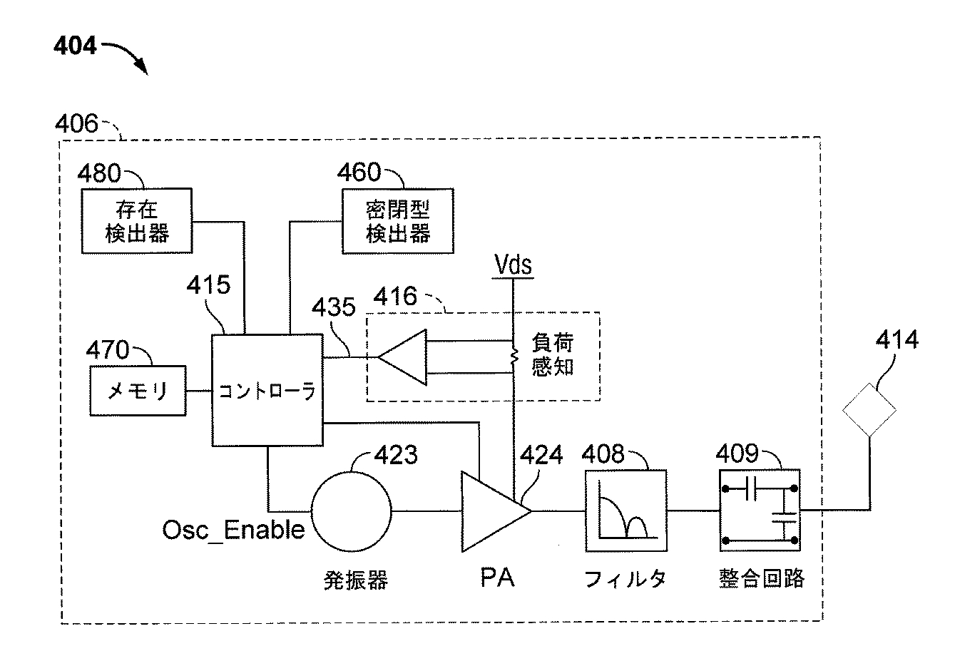
図4は、本発明の例示的な実施形態による、図1のワイヤレス電力伝達システムに使用され得る送信機404の機能ブロック図である。送信機404は、送信回路406および送信アンテナ414を含むことができる。送信アンテナ414は、図3に示すアンテナ352である可能性がある。送信回路406は、送信アンテナ414の周りにエネルギー(たとえば、磁束)を発生させる発振信号を生成することにより、送信アンテナ414にRF電力を供給してよい。送信機404は、任意の適切な周波数で動作することができる。例として、送信機404は、6.78MHzのISMバンドで動作することができる。
FIG. 4 is a functional block diagram of a
送信回路406は、送信回路406のインピーダンス(たとえば、50オーム)を送信アンテナ414に整合させるための固定インピーダンス整合回路409と、高調波放射を受信機108(図1)に結合されたデバイスの自己ジャミングを防ぐレベルまで低減させるように構成されたローパスフィルタ(LPF)408とを含んでよい。他の例示的な実施形態は、ノッチフィルタを含むが、それに限定されない異なるフィルタトポロジを含んでよく、ノッチフィルタは、特定の周波数を減衰させる一方で、他の周波数は通過させ、アンテナ414への出力電力、またはドライバ回路424によって引き出されるDC電流など、測定可能な送電メトリックに基づいて変化し得る、適応インピーダンス整合を含んでよい。送信回路406は、発振器423によって決定されるRF信号を駆動するように構成されたドライバ回路424をさらに含む。送信回路406は、個別のデバイスまたは回路から構成されても、または代わりに、一体型アセンブリから構成されてもよい。送信アンテナ414から出力される例示的なRF電力は、2.5ワット程度であってよい。
The
送信回路406は、発振器423の周波数または位相を調整し、かつ取り付けられた受信機を介して隣接するデバイスと対話するための通信プロトコルを実装するように出力電力レベルを調整するために、特定の受信機の送信フェーズ(またはデューティサイクル)の間に発振器423を選択的に有効にするためのコントローラ415をさらに含んでよい。コントローラ415は、本明細書ではプロセッサ415と呼ばれることもあることに留意されたい。発振器位相および送信経路内の関連する回路の調整により、特に、ある周波数から別の周波数に移行する際の帯域外放射の低減が可能になり得る。
Transmit
送信回路406は、送信アンテナ414によって生成された近接場の近傍における作動中の受信機の有無を検出するための負荷感知回路416をさらに含んでよい。例として、負荷感知回路416は、以下でさらに説明するように、送信アンテナ414によって生成された場の近傍における作動中の受信機の有無によって影響を及ぼされ得るドライバ回路424に流れる電流を監視する。ドライバ回路424上の負荷に対する変化の検出は、エネルギーを伝送するために発振器423を有効にすべきかどうか、および作動中の受信機と通信すべきかどうかを決定する際に使用するためにコントローラ415によって監視される。以下でより十分に説明するように、ドライバ回路424で測定される電流は、無効なデバイスが送信機404のワイヤレス電力伝達領域内に位置するかどうかを判定するために使用され得る。
Transmit
送信アンテナ414は、リッツ線とともに、または抵抗損を低く保つために選択された厚さ、幅、および金属のタイプを有するアンテナストリップとして実装され得る。一実装形態では、送信アンテナ414は、一般にテーブル、マット、ランプ、または他の携帯性の低い構成などの、より大きい構造と関連付けて構成され得る。したがって、送信アンテナ414は、一般に実用的な寸法となるように「巻くこと」を必要としない場合がある。送信アンテナ414の例示的な実装形態は、「電気的に小型」(すなわち、波長の数分の一)であり、共振周波数を規定するためにキャパシタを使用することにより、より低い使用可能な周波数で共振するように同調され得る。
The transmit
送信機404は、送信機404に関連し得る受信機デバイスの所在および状態に関する情報を収集および追跡してよい。したがって、送信回路406は、(本明細書ではプロセッサとも呼ばれる)コントローラ415に接続される、存在検出器480、密閉型検出器460、またはこれらの組合せを含んでよい。コントローラ415は、存在検出器480および密閉型検出器460からの存在信号に応答してドライバ回路424により送出される電力量を調整してよい。送信機404は、たとえば、ビル内にある従来のAC電力を変換するためのAC-DCコンバータ(図示せず)、従来のDC電源を送信機404に適した電圧に変換するためのDC-DCコンバータ(図示せず)などのいくつかの電源を介して、または従来のDC電源(図示せず)から直接電力を受け取ってよい。
The
非限定的な例として、存在検出器480は、送信機404のカバー領域に挿入される、充電されるべきデバイスの最初の存在を感知するために利用される運動検出器であってよい。検出後に、送信機404をオンにすることができ、デバイスによって受信されたRF電力を用いて、所定の方法でRxデバイス上のスイッチを切り替えることができ、それにより、結果として送信機404の駆動点インピーダンスが変化する。
As a non-limiting example,
別の非限定的な例として、存在検出器480は、たとえば、赤外線検出手段、運動検出手段、または他の適切な手段によって人を検出することが可能な検出器であってよい。いくつかの例示的な実施形態では、送信アンテナ414が特定の周波数で送信することができる電力量を制限する規定が存在してよい。場合によっては、これらの規定は、人を電磁放射から守ることを意図されている。しかしながら、送信アンテナ414が、たとえば、ガレージ、工業の現場、店舗などの、人によって占有されないか、または人によって占有される頻度が低い領域に位置する環境が存在し得る。これらの環境に人間がいない場合は、通常の電力制限規定を超えて送信アンテナ414の電力出力を増加させることを許容し得る。言い換えれば、コントローラ415は、人の存在に応答して、送信アンテナ414の電力出力を、規制レベルまたはそれ未満に調整し、人が送信アンテナ414の電磁場から規制距離の外側にいる場合は、送信アンテナ414の電力出力を、規制レベルを超えるレベルに調整してよい。
As another non-limiting example,
非限定的な例として、密閉型検出器460(本明細書では、密閉型コンパートメント検出器または密閉型空間検出器と呼ばれることもある)は、包囲体が閉状態または開状態であることを判定するための感知スイッチなどのデバイスであってよい。送信機が閉状態の包囲体内にあるとき、送信機の電力レベルを増加させてよい。 As a non-limiting example, a sealed detector 460 (sometimes referred to herein as a sealed compartment detector or a sealed spatial detector) determines that the enclosure is closed or open. It may be a device such as a sensing switch for When the transmitter is in a closed enclosure, the transmitter power level may be increased.
例示的な実施形態では、送信機404がいつまでもオンのままではない方法を使用してよい。この場合、送信機404は、ユーザによって決定された時間量の後、シャットオフされるようにプログラムされ得る。この特徴は、送信機404の周囲のワイヤレスデバイスが十分充電された後、送信機404、特にドライバ回路424が長く動作するのを防ぐ。このイベントは、リピータまたは受信アンテナ218より送信された、デバイスが十分充電されたという信号を検出するための回路の故障によるものである可能性がある。その周囲に別のデバイスが配置されている場合に、送信機404が自動的にシャットオフすることを防止するために、送信機404の自動シャットオフ機能は、その周囲で動作が検出されずに、定められた期間が経過した後にだけ、アクティブ化されてよい。ユーザが、望み通りに、無活動時間間隔を決定し、それを変更できてよい。非限定的な例として、この時間間隔は、特定のタイプのワイヤレスデバイスが最初に完全に放電したという仮定の下に、そのデバイスを完全に充電するのに必要な時間間隔よりも長くてよい。
In an exemplary embodiment, a method may be used in which
図5は、本発明の例示的な実施形態による、図1のワイヤレス電力伝達システムに使用され得る受信機508の機能ブロック図である。受信機508は、受信アンテナ518を含み得る受信回路510を含む。受信機508は、それに受信電力を提供するためのデバイス550にさらに結合する。受信機508は、デバイス550の外部にあるものとして示されているが、デバイス550に統合されてよいことに留意されたい。エネルギーは、受信アンテナ518にワイヤレスに伝播され、次いで受信回路510の残りの部分を介してデバイス550に結合され得る。例として、充電デバイスには、モバイルフォン、携帯型音楽プレーヤ、ラップトップコンピュータ、タブレットコンピュータ、コンピュータ周辺デバイス、通信デバイス(たとえば、Bluetoothデバイス)、デジタルカメラ、補聴器(および他の医療用デバイス)などのデバイスが含まれ得る。
FIG. 5 is a functional block diagram of a
受信アンテナ518は、送信アンテナ414(図4)と同じ周波数で、または特定の周波数範囲内で共振するように同調され得る。受信アンテナ518は、送信アンテナ414と同様の寸法を有しても、または関連するデバイス550の寸法に基づいて異なるサイズを有してもよい。例として、デバイス550は、送信アンテナ414の直径または長さよりも小さい直径寸法または長さ寸法を有するポータブル電子デバイスであってよい。そのような例では、受信アンテナ518は、同調キャパシタ(図示せず)のキャパシタンス値を低減させ、受信コイルのインピーダンスを増加させるために多巻きコイルとして実装され得る。例として、受信アンテナ518は、アンテナの直径を最大化し、受信アンテナ518のループ巻き数(すなわち、巻回)および巻線間キャパシタンスを低減するために、デバイス550の実質的な外周の周りに配置されてよい。
Receive
受信回路510は、受信アンテナ518に対するインピーダンス整合を可能にしてよい。受信回路510は、受け取られたRFエネルギー源をデバイス550が使用するための充電電力に変換するための電力変換回路506を含む。電力変換回路506は、RF-DC変換器520を含み、DC-DC変換器522を含んでもよい。RF-DC変換器520は、受信アンテナ518で受信されたRFエネルギー信号を、Vrectで表される出力電圧を有する非交流電力に整流する。DC-DC変換器522(または他の電力調整器)は、整流されたRFエネルギー信号を、VoutおよびIoutによって表される出力電圧および出力電流を有する、デバイス550に適合するエネルギーポテンシャル(たとえば、電圧)に変換する。部分的および完全な整流器、調整器、ブリッジ、ダブラー、ならびにリニア変換器およびスイッチング変換器を含む、様々なRF-DC変換器が企図される。
Receive
受信回路510は、受信アンテナ518を電力変換回路506に接続するための、あるいは電力変換回路506を切断するための、スイッチング回路512をさらに含んでよい。電力変換回路506から受信アンテナ518を切断することにより、デバイス550の充電を中断するだけでなく、送信機404(図2)から「見た」「負荷」も変化する。
The receiving
上記で開示したように、送信機404は、送信機ドライバ回路424に供給されるバイアス電流の変動を検出することができる負荷感知回路416を含む。したがって、送信機404は、受信機が送信機の近接場内に存在することを判定するための機構を有する。
As disclosed above, the
複数の受信機508が送信機の近接場内に存在するとき、他の受信機をより効率的に送信機に結合させるために、1つまたは複数の受信機の装荷および除荷を時間多重化することが望ましい場合がある。受信機508はまた、他の近くの受信機への結合を解消するか、または近くの送信機への装荷を低減させるためにクローキングされ得る。受信機のこの「除荷」は、本明細書では「クローキング」としても知られる。さらに、受信機508によって制御され送信機404によって検出される、除荷と装荷との間のこのスイッチングは、以下でより十分に説明するように、受信機508から送信機404への通信機構を実現することができる。加えて、受信機508から送信機404にメッセージを送信することを可能にするプロトコルが、このスイッチングに関連付けられ得る。例として、スイッチング速度は、100μ秒程度であってよい。
When
例示的な実施形態では、送信機404と受信機508との間の通信は、従来の双方向通信(すなわち、結合場を使用したバンド内信号伝達)ではなく、デバイス感知/充電制御機構を指す。言い換えれば、送信機404は、エネルギーが近接場で利用可能であるかどうかを調整するために送信信号のオン/オフキーイングを使用してよい。受信機は、これらのエネルギー変化を送信機404からのメッセージとして解釈してよい。受信機側から、受信機508は、どれくらいの電力が場から受け入れられているかを調整するために受信アンテナ518の同調および非同調を使用してよい。場合によっては、同調および非同調は、スイッチング回路512を介して実現され得る。送信機404は、場からの使用される電力のこの差を検出し、これらの変化を受信機508からのメッセージとして解釈してよい。送信電力の変調および負荷挙動の他の形態を利用してよいことに留意されたい。
In the exemplary embodiment, communication between
受信回路510は、送信機から受信機への情報信号伝達に対応し得る、受信エネルギーの変動を識別するために使用される、信号伝達検出器/ビーコン回路514をさらに含んでよい。さらに、信号伝達/ビーコン回路514は、低減されたRF信号エネルギー(すなわち、ビーコン信号)の送信を検出し、かつ低減されたRF信号エネルギーを公称電力に整流し、受信回路510内の電力を供給されていない回路または電力が枯渇した回路のいずれかを呼び起こして受信回路510をワイヤレス充電が可能なように構成するために使用されてもよい。
The receiving
受信回路510は、本明細書で説明するスイッチング回路512の制御を含む、本明細書で説明する受信機508のプロセスを調整するためのプロセッサ516をさらに含む。また、受信機508のクローキングは、充電電力をデバイス550に提供する外部の有線充電ソース(たとえば、壁コンセント/USB電力)の検出を含む他のイベントが発生したときにも行われる可能性がある。プロセッサ516は、受信機のクローキングを制御するのに加えて、ビーコン回路514を監視してビーコン状態を判定し、送信機404から送信されたメッセージを抽出してもよい。プロセッサ516は、性能の改善のためにDC-DC変換器522を調整してもよい。
The
図6は、図4の送信回路406に使用され得る送信回路600の一部分の概略図である。送信回路600は、上記に図4において説明したように、ドライバ回路624を含んでよい。上述のように、ドライバ回路624は、矩形波を受け取り、送信回路650に供給する正弦波を出力するように構成され得るスイッチング増幅器であってよい。場合によっては、ドライバ回路624は、増幅器回路と呼ばれることがある。ドライバ回路624は、E級増幅器として示されているが、本発明の実施形態によって任意の適切なドライバ回路624が使用されてよい。ドライバ回路624は、図4に示されるように、発振器423からの入力信号602によって駆動することができる。また、ドライバ回路624は、送信回路650を介して送出され得る最大電力を制御するように構成された駆動電圧VDを提供され得る。高調波を解消または低減させるために、送信回路600は、フィルタ回路626を含んでよい。フィルタ回路626は、3極(キャパシタ634、インダクタ632、およびキャパシタ636)ローパスフィルタ回路626であってよい。
FIG. 6 is a schematic diagram of a portion of a transmit
フィルタ回路626によって出力された信号は、アンテナ614を含む送信回路650に提供され得る。送信回路650は、ドライバ回路624によって供給されるフィルタ処理済み信号の周波数で共振する可能性がある、(たとえば、アンテナのインダクタンスもしくはキャパシタンス、または追加のキャパシタ構成要素に起因する可能性がある)あるキャパシタンス620およびインダクタンスを有する直列共振回路を含んでよい。送信回路650の負荷は、可変抵抗器622によって表すことができる。この負荷は、送信回路650から電力を受け取るように置かれたワイヤレス電力受信機508の関数であってよい。
The signal output by the
たとえばワイヤレス電力伝達システム100などのワイヤレス電力伝達システムにおいて、時間変動電磁界は、送信機(たとえば、送信機104)によって生成され、受信機(たとえば、受信機108)は、電力伝達のために電磁界に結合する。受信機は、通常、データ通信のために通信トランシーバ(たとえば、近接場通信(NFC)トランシーバ)を利用することもできるワイヤレスデバイス(たとえば、モバイルハンドセット、タブレットなど)内で見つかる。ワイヤレス電力伝達システムおよびNFCシステムが誘導電力伝達の類似の原理で働くので、これは、ワイヤレス電力受信機およびNFCトランシーバが同じアンテナコイルを共有する場合、コストおよびエリアの視点から有益である。
In a wireless power transfer system, such as wireless
しかしながら、アンテナコイルを共有することに関する問題がいくつかあり得る。たとえば、ワイヤレス伝達される電力の電力レベルは、NFC回路に損傷を与える、および/またはNFC回路を破壊するのに十分高い可能性があった。ある期間の間(たとえば、電力レベルが高すぎるとき)、信号がNFC回路に移動することをブロックするスイッチが導入され得るが、高電力レベルを処理するために、スイッチのサイズは大きくなければならないことになる。従来のシステムでは、受信機のアンテナによって受信される信号(たとえば、送信機から受信機に伝達される電力)が、ワイヤレス電力伝達システムまたはNFC回路に、スイッチを介して移動するので、スイッチが高電力レベルを処理することができることが望ましいことになる。大きい低損失スイッチは、一般に高価であり、家庭用電化製品では上手く適合しない(たとえば、それらはハンドセットなどの電子機器では高すぎるので)。小さいスイッチは、高損失を有しており、システム性能を低下させる。事実上、任意の追加の構成要素をワイヤレス電力伝達システムおよび/またはNFC回路に追加することは、(たとえば、信号経路に存在する追加の構成要素に関連した余分の遅延および損失により)システム効率を低下させる。別の例として、NFC回路は、ワイヤレス電力伝達システムの効率を低下させる可能性がある。別の例として、ワイヤレス電力伝達回路は、NFCシステムの性能および/または範囲を低下させる可能性がある。 However, there can be some problems with sharing antenna coils. For example, the power level of wireless transmitted power could be high enough to damage and / or destroy the NFC circuit. A switch may be introduced that blocks the signal from moving to the NFC circuit for a period of time (eg when the power level is too high), but the switch size must be large to handle the high power level It will be. In conventional systems, the signal received by the receiver antenna (e.g., power transferred from the transmitter to the receiver) travels through the switch to the wireless power transfer system or NFC circuit, so the switch is high. It would be desirable to be able to handle power levels. Large, low loss switches are generally expensive and do not fit well in home appliances (for example, they are too expensive for electronic devices such as handsets). Small switches have high losses and degrade system performance. In effect, adding any additional components to the wireless power transfer system and / or NFC circuit can reduce system efficiency (e.g., due to extra delays and losses associated with additional components present in the signal path). Reduce. As another example, NFC circuits can reduce the efficiency of wireless power transfer systems. As another example, a wireless power transfer circuit may reduce the performance and / or range of an NFC system.
これらの問題を軽減するために、アンテナと通信システムとの間、およびアンテナとワイヤレス電力伝達システムとの間の信号経路における任意の追加の構成要素の追加無しに、通信システム(たとえば、NFCシステム)およびワイヤレス電力伝達システムの共存を可能にする受信機が提案される。 To alleviate these problems, a communication system (e.g., NFC system) without the addition of any additional components in the signal path between the antenna and the communication system and between the antenna and the wireless power transfer system. And a receiver that allows coexistence of wireless power transfer systems is proposed.
図7は、図1のワイヤレス電力伝達システム100で使用され得る受信機700の別の機能ブロック図である。図7に図示したように、受信機700は、アンテナ702、アンテナ同調、過電圧保護、および整流器回路(antenna tuning, overvoltage protection, and rectifier circuit)704、DC-DCコンバータ714、ワイヤレス電力回路724、コントローラ708、通信回路706、ならびに/または通信チップ716を含む。
FIG. 7 is another functional block diagram of a
一実施形態では、アンテナ同調、過電圧保護、および整流器回路704は、その中の構成要素に損傷を与える可能性がある高電力レベルからDC-DCコンバータ714およびワイヤレス動力回路724を保護するように構成される。アンテナ同調、過電圧保護、および整流器回路704は、アンテナ702から受信された信号を整流し、整流された信号をDC-DCコンバータ714、および最終的にワイヤレス電力回路724に転送する(たとえば、ワイヤレス動力回路724が充電操作を実行することができるように)整流器を含み得る。アンテナ同調、過電圧保護、および整流器回路704、DC-DCコンバータ714、ならびにワイヤレス電力回路724は、たとえば送信機104などの送信機から電力をワイヤレスに受け取るために使用され得る。通信回路706および通信チップ716は、NFC通信のために使用され得る。通信回路706は、アンテナ702から受信された信号を通信チップ716に転送し得る。
In one embodiment, antenna tuning, overvoltage protection, and
アンテナ702は、アンテナ同調、過電圧保護、および整流器回路704と通信回路706との両方に結合される。一実施形態では、コントローラ708は、アンテナ同調、過電圧保護、および整流器回路704を介したアンテナ702とDC-DCコンバータ714との間の経路、または通信回路706を介したアンテナ702と通信チップ716との間の経路を使用可能にするように構成される。コントローラ708は、アンテナ同調、過電圧保護、および整流器回路704、ならびに/または通信回路706における構成要素を制御することによって、いずれかの経路を使用可能にすることができ、これについては、図8A〜図8Bに関して以下でより詳細に説明する。
図8Aは、図1のワイヤレス電力伝達システム100で使用され得る受信機700のより詳細な機能ブロック図である。図8Aに図示したように、受信機700は、アンテナ702(たとえば、インダクタまたはコイル)、アンテナ同調、過電圧保護、および整流器回路704、DC-DCコンバータ714、通信回路706、通信チップ716、ならびにコントローラ708を含む。上述したように、アンテナ同調、過電圧保護、および整流器回路704、ならびに通信回路706は、アンテナ702を共有する。
FIG. 8A is a more detailed functional block diagram of a
アンテナ同調、過電圧保護、および整流器回路704は、4つの同調キャパシタ802、804、810、および812、過電圧保護(OVP)回路、ならびに整流器回路を含み得る。OVP回路は、2つのスイッチ806および808(たとえば、トランジスタ、またはリレーなど任意の低損失スイッチ)を含み得る。整流器回路は、ダイオード814、816、818、および820を含み得る。
The antenna tuning, overvoltage protection, and
通信回路706は、2つの同調キャパシタ830および832、2つのノッチインダクタ822および824、2つのノッチフィルタ(たとえば、バンドストップノッチフィルタ)、ならびに2つのスイッチ826および828(たとえば、トランジスタ、またはリレーなど任意の低損失スイッチ)を含み得る。第1のノッチフィルタは、キャパシタ836と並列して結合されるインダクタ834を含む(たとえば、本明細書で共振ネットワークと呼ぶ)。第2のノッチフィルタは、キャパシタ840(たとえば、本明細書で共振ネットワークと呼ぶ)と並列して結合されるインダクタ838を含む。一実施形態では、同調キャパシタ830および第1のノッチフィルタは、通信回路706の正の分岐の一部であり、同調キャパシタ832および第2のノッチフィルタは、通信回路706の負の分岐の一部である。
一実施形態では、同調キャパシタ802およびノッチインダクタ822は、本明細書では共振ネットワークと呼ぶ。同様に、同調キャパシタ804およびノッチインダクタ824は、本明細書では共振ネットワークと呼ぶ。
In one embodiment, tuning
スイッチ806、808、826、および828は、コントローラ708によって制御され得る。たとえば、コントローラ708は、スイッチ806および808を制御するOVP信号を出力し、スイッチ826および828を制御する通信制御信号を出力する。図8Aに図示したように、スイッチ806および808は、アンテナ702とDC-DCコンバータ714との間の信号経路内に位置しない。同様に、スイッチ826および828は、アンテナ702と通信チップ716との間の信号経路内に位置しない。以下でより詳細に説明するように、スイッチ806、808、826、および828は、代わりに、1つまたは複数の共振ネットワークを同調する、またはチューンアウトするように構成され、1つまたは複数の共振ネットワークは、アンテナ702から発信する信号の方向を決定するように構成される。
The
一実施形態では、ワイヤレス電力動作のために受け取られた電力は、6.78MHzの周波数で受け取られてもよく、データ通信(たとえば、NFC)動作のために受け取られた電力は、13.56MHzの周波数で受け取られ得る。全4つのスイッチ806、808、826、および828がオープン(たとえば、コントローラ708によって非アクティブ化される、または使用不能にされる)のとき、アンテナ702によってワイヤレスで受け取られる電力は、DC-DCコンバータ714に送られ、通信チップ716には送られない。第1のノッチフィルタのインダクタ834およびキャパシタ836の並列組合せは、6.78MHzで共振するように同調され得る。第2のノッチフィルタのインダクタ838およびキャパシタ840の並列組合せは、6.78MHzで共振するように同調され得る。したがって、ワイヤレス充電が行われる周波数は、次のように表すことができる。
一実施形態では、スイッチ826および828がオープンであるので、アンテナ702から移動する信号のためのアンテナ702ならびにノッチインダクタ822および824によって共有されるノードにおけるインピーダンスは高い(たとえば、通信チップ716の方向を調査するとき)。アンテナ同調、過電圧保護、および整流器回路704において追加の構成要素がないので、ワイヤレス電力伝達の効率は、ほぼ不変のままである。
In one embodiment, since
同様に、全4つのスイッチ806、808、826、および828がクローズ(たとえば、コントローラ708によってアクティブ化される、または使用可能にされる)のとき、アンテナ702によってワイヤレスで受け取られる電力は、通信チップ716に送られ、DC-DCコンバータ714には送られない。たとえば、13.56MHzで信号が受信され、全4つのスイッチ806、808、826、および828がクローズのとき、アンテナ702からDC-DCコンバータ714への経路は、(たとえば、同調キャパシタ802およびノッチインダクタ822の並列組合せ、ならびに同調キャパシタ804およびノッチインダクタ824の並列組合せが13.56MHzの共振周波数でバンドストップノッチフィルタのように作動するので)アンテナ702から通信チップ716への経路よりも高いインピーダンスを有するように見え得る。全4つのスイッチ806、808、826、および828がクローズの実施形態は、図8Bに関して以下でより詳細に説明する。
Similarly, when all four
図8Bは、図1のワイヤレス電力伝達システム100で使用され得る受信機700の別のより詳細な機能ブロック図である。特に、図8Bは、全4つのスイッチ806、808、826、および828がクローズのときの受信機700のモデルを示す。図8Bに図示したように、スイッチ806、808、826、および828は、クローズのとき短絡されるように見えるので、スイッチ806、808、826、および828は存在しない。
FIG. 8B is another more detailed functional block diagram of a
上述したように、同調キャパシタ802およびノッチインダクタ822の並列組合せ、ならびに同調キャパシタ804およびノッチインダクタ824の並列組合せのインダクタンスおよびキャパシタンス値は、並列組合せがデータ通信周波数(たとえば、13.56MHz)で共振するように選択される。したがって、スイッチ806、808、826、および828クローズなので、(たとえば、DC-DCコンバータ714の方向を調査するとき)アンテナ702から移動する信号について、アンテナ702と、同調キャパシタ802およびノッチインダクタ822の並列組合せとによって共有されるノードにおけるインピーダンス、ならびにアンテナ702と、同調キャパシタ804およびノッチインダクタ824の並列組合せとによって共有されるノードにおけるインピーダンスは高い。したがって、データ通信が行われる周波数は、次のように表すことができる。
より長いデータ通信距離、および/またはより信頼性が高い通信が望まれる場合、磁界強度を増加させることができる。これは、データ通信周波数(たとえば、13.56MHz)でアンテナ702コイル電流を増加させることによって達成することができる。アンテナ702コイル電流は、同調キャパシタ830および/または832を使用して増加させることができ、これによって、アンテナ702は、そのデータ通信周波数で低いインピーダンス経路であるように見える。同調キャパシタ830および/または832は、そのデータ通信周波数でアンテナ702と第1のノッチフィルタおよび/または第2のノッチフィルタとの間の反応差を相殺することができる。この反応差は、次のように表すことができる。
このようにして、これらの実施形態の利点は、以下のように、(1)ワイヤレス電力伝達システム(たとえば、アンテナ同調、過電圧保護、および整流器回路704、DC-DCコンバータ714、ならびにワイヤレス電力回路724)の効率のごくわずかな低下、(2)データ通信システム(たとえば、通信回路706および通信チップ716)の性能のごくわずかな低下、ならびに(3)追加の構成要素が既存のワイヤレス電力伝達回路または既存のデータ通信回路に追加される必要がないことによる、およびアンテナ702が共有されることによるコストの低下であり得る。
Thus, the advantages of these embodiments include: (1) a wireless power transfer system (eg, antenna tuning, overvoltage protection and
図9は、電力をワイヤレスに受け取るための例示的な方法900のフローチャートである。一実施形態では、フローチャート900におけるステップは、受信機(たとえば、図7の受信機700)によって実行され得る。フローチャート900の方法について、特定の順序を参照して本明細書で説明するが、様々な実施形態では、本明細書のブロックが異なる順序で実施されるか、または省略される場合があり、さらなるブロックが追加される場合がある。フローチャート900の方法がデータ通信を受信または送信するように構成され得る別のデバイスおよび/または任意のデバイスから電力をワイヤレスに受け取るように構成され得る任意のデバイスにおいて実施されてよいことが当業者には了解されよう。
FIG. 9 is a flowchart of an
ブロック902で、電力がアンテナを介して送信機からワイヤレスで受け取られる。一実施形態では、アンテナは、第1の経路に沿って第1の共振ネットワークを介してワイヤレス電力回路に結合される。さらなる実施形態では、ワイヤレス電力回路は、第1の周波数に従って動作するように構成される。さらなる実施形態では、アンテナは、第2の経路に沿って第2の共振ネットワークを介して通信回路にさらに結合される。さらなる実施形態では、通信回路は、第2の周波数に従って動作するように構成される。さらなる実施形態では、第1の経路は、第2の周波数で第2の経路よりも高いインピーダンスを有する。さらなる実施形態では、第1の経路は、第1の周波数で第2の経路よりも低いインピーダンスを有する。ブロック904で、どの経路がより低いインピーダンスを有するかに基づいて、第1の経路または第2の経路に沿って電力が伝達される。
At
図10は、例示的な一実施形態による受信機1000の機能ブロック図である。受信機1000は、本明細書に記載される様々なアクションのための手段1002と手段1004とを備える。受信機1000は、電力を送信機からワイヤレスに受け取るための手段1002を含む。一実施形態では、電力を送信機からワイヤレスに受け取るための手段1002は、上記にブロック902に関して説明した機能のうちの1つまたは複数を実施するように構成され得る。受信機1000は、どの経路がより低いインピーダンスを有するかに基づいて、第1の経路または第2の経路に沿って電力を伝達するための手段1004をさらに含む。一実施形態では、どの経路がより低いインピーダンスを有しているかに基づいて、第1の経路または第2の経路に沿って電力を伝達するための手段1004は、ブロック904に関して上記で説明した機能のうちの1つまたは複数を実行するように構成され得る。
FIG. 10 is a functional block diagram of a
上記で説明した方法の様々な動作は、様々なハードウェア構成要素および/もしくはソフトウェア構成要素、回路、ならびに/またはモジュールなどの、その動作を実行することが可能な任意の適切な手段によって実行され得る。一般に、図に示す任意の動作は、その動作を実行することが可能な対応する機能的手段によって実行され得る。電力を受け取るための手段は、アンテナ702を備える。電力を伝達するための手段は、アンテナ702を備える。
The various operations of the methods described above are performed by any suitable means capable of performing the operations, such as various hardware and / or software components, circuits, and / or modules. obtain. In general, any operation shown in the figures may be performed by corresponding functional means capable of performing the operation. The means for receiving power comprises an
多種多様な技術および技法のうちのいずれかを使用して情報および信号を表すことができる。たとえば、上記の説明全体にわたって言及され得るデータ、命令、コマンド、情報、信号、ビット、シンボル、およびチップは、電圧、電流、電磁波、磁界または磁性粒子、光場または光学粒子、あるいはそれらの任意の組合せによって表され得る。 Information and signals can be represented using any of a wide variety of techniques and techniques. For example, data, instructions, commands, information, signals, bits, symbols, and chips that may be referred to throughout the above description are voltages, currents, electromagnetic waves, magnetic fields or magnetic particles, light fields or optical particles, or any of them Can be represented by a combination.
本明細書で開示する実施形態に関して説明する様々な例示的な論理ブロック、モジュール、回路、およびアルゴリズムステップは、電子ハードウェア、コンピュータソフトウェア、またはその両方の組合せとして実装され得る。ハードウェアおよびソフトウェアのこの互換性を明確に示すために、様々な例示的な構成要素、ブロック、モジュール、回路、およびステップについて、上記に概してそれらの機能に関して説明した。そのような機能をハードウェアとして実装するか、ソフトウェアとして実装するかは、特定の適用例および全体的なシステムに課される設計制約に依存する。説明した機能を特定の適用例ごとに様々な方法で実装し得るが、そのような実装形態の決定は、本発明の実施形態の範囲からの逸脱を生じるものと解釈すべきではない。 Various exemplary logic blocks, modules, circuits, and algorithm steps described with respect to the embodiments disclosed herein may be implemented as electronic hardware, computer software, or a combination of both. To clearly illustrate this interchangeability of hardware and software, various illustrative components, blocks, modules, circuits, and steps have been described above generally in terms of their functionality. Whether such functionality is implemented as hardware or software depends upon the particular application and design constraints imposed on the overall system. Although the described functionality may be implemented in a variety of ways for a particular application, such implementation determination should not be construed as a departure from the scope of the embodiments of the present invention.
本明細書で開示する実施形態に関して説明する様々な例示的なブロック、モジュール、および回路は、汎用プロセッサ、デジタルシグナルプロセッサ(DSP)、特定用途向け集積回路(ASIC)、フィールドプログラマブルゲートアレイ(FPGA)もしくは他のプログラマブル論理デバイス、個別ゲートもしくはトランジスタ論理、個別ハードウェア構成要素、または、本明細書で説明する機能を実行するように設計されたそれらの任意の組合せで、実装または実行されてよい。汎用プロセッサはマイクロプロセッサであり得るが、代替として、プロセッサは、任意の従来のプロセッサ、コントローラ、マイクロコントローラ、またはステートマシンであり得る。プロセッサはまた、コンピューティングデバイスの組合せ、たとえば、DSPとマイクロプロセッサとの組合せ、複数のマイクロプロセッサ、DSPコアと連携する1つまたは複数のマイクロプロセッサ、あるいは任意の他のそのような構成として実装され得る。 Various exemplary blocks, modules, and circuits described with respect to the embodiments disclosed herein include general purpose processors, digital signal processors (DSPs), application specific integrated circuits (ASICs), field programmable gate arrays (FPGAs). Alternatively, it may be implemented or implemented with other programmable logic devices, individual gate or transistor logic, individual hardware components, or any combination thereof designed to perform the functions described herein. A general purpose processor may be a microprocessor, but in the alternative, the processor may be any conventional processor, controller, microcontroller, or state machine. A processor may also be implemented as a combination of computing devices, eg, a DSP and microprocessor combination, multiple microprocessors, one or more microprocessors in conjunction with a DSP core, or any other such configuration. obtain.
本明細書で開示された実施形態に関連して記載された方法またはアルゴリズムおよび機能のステップは、直接ハードウェアで具現化されても、またはプロセッサによって実行されるソフトウェアモジュールで具現化されても、またはその2つの組合せで具現化されてもよい。ソフトウェアで実装する場合、機能は、1つもしくは複数の命令またはコードとして有形の非一時的コンピュータ可読媒体上に記憶されるか、あるいは非一時的コンピュータ可読媒体を介して送信され得る。ソフトウェアモジュールは、ランダムアクセスメモリ(RAM)、フラッシュメモリ、読取り専用メモリ(ROM)、電気的プログラマブルROM(EPROM)、電気消去可能プログラマブルROM(EEPROM)、レジスタ、ハードディスク、リムーバブルディスク、CD-ROM、または、当技術分野で既知の任意の他の形態の記憶媒体中に常駐し得る。記憶媒体は、プロセッサが記憶媒体から情報を読み取り、記憶媒体に情報を書き込むことができるように、プロセッサに結合される。代替として、記憶媒体はプロセッサと一体であり得る。本明細書で使用する場合、ディスク(disk)およびディスク(disc)は、コンパクトディスク(disc)(CD)、レーザーディスク(登録商標)(disc)、光ディスク、デジタル多用途ディスク(disc)(DVD)、フロッピー(登録商標)ディスク(disk)、およびブルーレイディスク(disc)を含み、ディスク(disk)は、通常、磁気的にデータを再生し、ディスク(disc)は、レーザーで光学的にデータを再生する。上記の組合せも、コンピュータ可読媒体の範囲の中に含まれるべきである。プロセッサおよび記憶媒体はASIC中に常駐し得る。ASICはユーザ端末中に常駐し得る。代替として、プロセッサおよび記憶媒体は、ユーザ端末中に個別構成要素として常駐し得る。 The method or algorithm and functional steps described in connection with the embodiments disclosed herein may be implemented directly in hardware or in software modules executed by a processor, Or it may be embodied by a combination of the two. When implemented in software, the functions may be stored on or transmitted over as a tangible non-transitory computer-readable medium as one or more instructions or code. Software module can be random access memory (RAM), flash memory, read only memory (ROM), electrically programmable ROM (EPROM), electrically erasable programmable ROM (EEPROM), register, hard disk, removable disk, CD-ROM, or May reside in any other form of storage medium known in the art. A storage medium is coupled to the processor such that the processor can read information from, and write information to, the storage medium. In the alternative, the storage medium may be integral to the processor. As used herein, a disc and a disc are a compact disc (CD), a laser disc (registered trademark) (disc), an optical disc, a digital versatile disc (DVD). , Floppy disks, and blu-ray discs, which usually reproduce data magnetically, and the disc optically reproduces data with a laser To do. Combinations of the above should also be included within the scope of computer-readable media. The processor and the storage medium can reside in an ASIC. The ASIC can reside in the user terminal. In the alternative, the processor and the storage medium may reside as discrete components in a user terminal.
本開示の概要を述べるために、本発明のいくつかの態様、利点、および新規の特徴について本明細書で説明してきた。本発明の任意の特定の実施形態に従って、そのような利点の必ずしもすべてを実現できない場合があることを理解されたい。したがって、本発明は、本明細書に教示される1つの利点または利点の群を、本明細書に教示または示唆され得る他の利点を必ずしも実現することなく実現または最適化するように具体化または実行され得る。 For purposes of summarizing the present disclosure, certain aspects, advantages, and novel features of the invention have been described herein. It should be understood that not all such advantages may be realized in accordance with any particular embodiment of the present invention. Accordingly, the present invention may be embodied or optimized to realize or optimize one advantage or group of advantages taught herein without necessarily realizing the other advantages that may be taught or suggested herein. Can be executed.
上述の実施形態への様々な修正が容易に明らかになり、本明細書に定義する一般原理は、本発明の趣旨または範囲を逸脱することなく他の実施形態に適用され得る。したがって、本発明は、本明細書に示された実施形態に限定されるものではなく、本明細書に開示された原理および新規の特徴に一致する最大の範囲を与えるものである。 Various modifications to the above-described embodiments will be readily apparent and the general principles defined herein may be applied to other embodiments without departing from the spirit or scope of the invention. Accordingly, the present invention is not limited to the embodiments shown herein, but provides the greatest scope consistent with the principles and novel features disclosed herein.
100 ワイヤレス電力伝達システム
102 入力電力
104 送信機
105 場
108 受信機
110 出力電力
112 距離
114 送信アンテナ
118 受信アンテナ
204 送信機
206 ワイヤレス場
206 送信回路
208 受信機
210 受信回路
214 送信アンテナ
218 受信アンテナ
219 通信チャネル
222 発振器
223 周波数制御信号
224 ドライバ回路
226 フィルタ/整合回路
232 整合回路
234 整流器/スイッチング回路
236 バッテリー
350 送信回路または受信回路
352 「ループ」アンテナ
354 キャパシタ
358 信号
404 送信機
406 送信回路
408 ローパスフィルタ(LPF)
409 固定インピーダンス整合回路
414 アンテナ
415 コントローラ
416 負荷感知回路
423 発振器
424 ドライバ回路
460 密閉型検出器
480 存在検出器
506 電力変換回路
508 受信機
510 受信回路
512 スイッチング回路
514 信号伝達検出器/ビーコン回路
516 プロセッサ
518 受信アンテナ
520 RF-DC変換器
522 DC-DC変換器
550 充電デバイス
600 送信回路
602 入力信号
614 アンテナ
620 キャパシタンス
622 可変抵抗器
624 ドライバ回路
626 フィルタ回路
632 インダクタ
634 キャパシタ
636 キャパシタ
650 送信回路
700 受信機
702 アンテナ
704 アンテナ同調、過電圧保護、および整流器回路
706 通信回路
708 コントローラ
714 DC-DCコンバータ
716 通信チップ
724 ワイヤレス電力回路
802 同調キャパシタ
804 同調キャパシタ
806 スイッチ
808 スイッチ
810 同調キャパシタ
812 同調キャパシタ
814 ダイオード
816 ダイオード
818 ダイオード
820 ダイオード
822 ノッチインダクタ
824 ノッチインダクタ
826 スイッチ
828 スイッチ
830 同調キャパシタ
832 同調キャパシタ
836 キャパシタ
1000 受信機
100 wireless power transfer system
102 Input power
104 transmitter
105 places
108 Receiver
110 Output power
112 distance
114 Transmit antenna
118 Receive antenna
204 Transmitter
206 Wireless field
206 Transmitter circuit
208 receiver
210 Receiver circuit
214 Transmit antenna
218 Receive antenna
219 communication channel
222 Oscillator
223 Frequency control signal
224 Driver circuit
226 Filter / matching circuit
232 matching circuit
234 Rectifier / Switching circuit
236 battery
350 Transmitter or receiver circuit
352 “Loop” Antenna
354 capacitors
358 signals
404 transmitter
406 Transmitter circuit
408 Low-pass filter (LPF)
409 Fixed impedance matching circuit
414 antenna
415 controller
416 Load sensing circuit
423 oscillator
424 Driver circuit
460 Sealed detector
480 Presence detector
506 Power conversion circuit
508 receiver
510 Receiver circuit
512 switching circuit
514 Signal detector / beacon circuit
516 processor
518 Receive antenna
520 RF-DC converter
522 DC-DC converter
550 charging device
600 Transmitter circuit
602 Input signal
614 Antenna
620 capacitance
622 variable resistor
624 Driver circuit
626 Filter circuit
632 inductor
634 capacitors
636 capacitor
650 transmitter circuit
700 receiver
702 antenna
704 Antenna tuning, overvoltage protection, and rectifier circuit
706 Communication circuit
708 controller
714 DC-DC converter
716 communication chip
724 wireless power circuit
802 Tuning capacitor
804 Tuning capacitor
806 switch
808 switch
810 Tuning capacitor
812 Tuning capacitor
814 diode
816 diodes
818 diode
820 diode
822 notch inductor
824 Notch inductor
826 switch
828 switch
830 Tuning capacitor
832 Tuning capacitor
836 capacitors
1000 receiver
Claims (32)
電力を送信機からワイヤレスに受け取るように構成されたアンテナと、
前記電力を負荷に供給するように構成されるとともに、第1の周波数に従って動作するように構成されたワイヤレス電力回路と、
第2の周波数に従って動作するように構成された通信回路と、
前記アンテナと前記ワイヤレス電力回路との間に結合されるとともに、前記アンテナと前記通信回路との間に結合された回路であって、前記回路が、第1の共振ネットワークと第2の共振ネットワークとを備え、前記回路が、前記第1の共振ネットワークを介した前記アンテナと前記ワイヤレス電力回路との間の第1の経路と、前記第2の共振ネットワークを介した前記アンテナと前記通信回路との間の第2の経路とを備え、前記第1の経路が、前記第2の周波数で前記第2の経路よりも高いインピーダンスを有し、前記第1の周波数で前記第2の経路よりも低いインピーダンスを有する、回路と
を備える受信機。 A receiver for receiving power wirelessly,
An antenna configured to receive power wirelessly from a transmitter;
A wireless power circuit configured to supply the power to a load and configured to operate according to a first frequency;
A communication circuit configured to operate according to a second frequency;
A circuit coupled between the antenna and the wireless power circuit and coupled between the antenna and the communication circuit, the circuit comprising: a first resonant network; a second resonant network; The circuit includes a first path between the antenna and the wireless power circuit via the first resonant network, and the antenna and the communication circuit via the second resonant network. A second path in between, wherein the first path has a higher impedance at the second frequency than the second path and is lower than the second path at the first frequency A receiver having a circuit with impedance.
アンテナを介して電力を送信機からワイヤレスに受け取るステップであって、前記アンテナが、第1の経路に沿って第1の共振ネットワークを介してワイヤレス電力回路に結合され、前記ワイヤレス電力回路が、第1の周波数に従って動作するように構成され、前記アンテナが、第2の経路に沿って第2の共振ネットワークを介して通信回路にさらに結合され、前記通信回路が、第2の周波数に従って動作するように構成され、前記第1の経路が、前記第2の周波数で前記第2の経路よりも高いインピーダンスを有し、前記第1の周波数で前記第2の経路よりも低いインピーダンスを有する、ステップと、
どの経路がより低いインピーダンスを有するかに基づいて、前記第1の経路または前記第2の経路に沿って前記電力を伝達するステップと
を含む方法。 A method for receiving power wirelessly,
Wirelessly receiving power from a transmitter via an antenna, wherein the antenna is coupled to a wireless power circuit via a first resonant network along a first path, the wireless power circuit being Configured to operate according to a frequency of 1, wherein the antenna is further coupled to a communication circuit via a second resonant network along a second path, so that the communication circuit operates according to a second frequency The first path has a higher impedance than the second path at the second frequency, and has a lower impedance than the second path at the first frequency; and ,
Transferring the power along the first path or the second path based on which path has a lower impedance.
電力を送信機からワイヤレスに受け取るための手段であって、電力をワイヤレスに受け取るための前記手段が、第1の経路に沿って第1の共振ネットワークを介して前記電力を負荷に供給するための手段に結合され、前記電力を負荷に供給するための前記手段が、第1の周波数に従って動作するように構成され、電力をワイヤレスに受け取るための前記手段が、第2の経路に沿って第2の共振ネットワークを介して前記電力を通信チップに供給するための手段にさらに結合され、前記電力を通信チップに供給するための前記手段が、第2の周波数に従って動作するように構成され、前記第1の経路が、前記第2の周波数で前記第2の経路よりも高いインピーダンスを有し、前記第1の周波数で前記第2の経路よりも低いインピーダンスを有する、手段と、
どの経路がより低いインピーダンスを有するかに基づいて、前記第1の経路または前記第2の経路に沿って前記電力を伝達するための手段と
を備える装置。 A device for receiving power wirelessly,
Means for wirelessly receiving power from a transmitter, wherein the means for wirelessly receiving power is for supplying the power to a load via a first resonant network along a first path. The means coupled to the means for supplying the power to the load is configured to operate according to a first frequency, and the means for wirelessly receiving the power is a second along the second path. Further coupled to means for supplying the power to the communication chip via a resonant network of, wherein the means for supplying the power to the communication chip is configured to operate according to a second frequency, Means having a higher impedance than the second path at the second frequency and a lower impedance than the second path at the first frequency; and
Means for transferring the power along the first path or the second path based on which path has a lower impedance.
アンテナを介して電力を送信機からワイヤレスに受け取ることであって、前記アンテナが、第1の経路に沿って第1の共振ネットワークを介してワイヤレス電力回路に結合され、前記ワイヤレス電力回路が、第1の周波数に従って動作するように構成され、前記アンテナが、第2の経路に沿って第2の共振ネットワークを介して通信回路にさらに結合され、前記通信回路が、第2の周波数に従って動作するように構成され、前記第1の経路が、前記第2の周波数で前記第2の経路よりも高いインピーダンスを有し、前記第1の周波数で前記第2の経路よりも低いインピーダンスを有する、受け取ることと、
どの経路がより低いインピーダンスを有するかに基づいて、前記第1の経路または前記第2の経路に沿って前記電力を伝達させることと
を行わせるコードを含む、非一時的コンピュータ可読記録媒体。 When executed, the device
Wirelessly receiving power from a transmitter via an antenna, wherein the antenna is coupled to a wireless power circuit via a first resonant network along a first path, the wireless power circuit being Configured to operate according to a frequency of 1, wherein the antenna is further coupled to a communication circuit via a second resonant network along a second path, so that the communication circuit operates according to a second frequency The first path has a higher impedance than the second path at the second frequency and has a lower impedance than the second path at the first frequency. When,
A non-transitory computer readable recording medium comprising code for causing the power to be transmitted along the first path or the second path based on which path has a lower impedance.
Applications Claiming Priority (3)
| Application Number | Priority Date | Filing Date | Title |
|---|---|---|---|
| US14/010,271 US9613747B2 (en) | 2013-08-26 | 2013-08-26 | System and method for efficient data communication and wireless power transfer coexistence |
| US14/010,271 | 2013-08-26 | ||
| PCT/US2014/050079 WO2015031016A1 (en) | 2013-08-26 | 2014-08-07 | System and method for efficient data communication and wireless power transfer coexistence |
Publications (3)
| Publication Number | Publication Date |
|---|---|
| JP2016536964A true JP2016536964A (en) | 2016-11-24 |
| JP2016536964A5 JP2016536964A5 (en) | 2017-08-31 |
| JP6382982B2 JP6382982B2 (en) | 2018-08-29 |
Family
ID=51392415
Family Applications (1)
| Application Number | Title | Priority Date | Filing Date |
|---|---|---|---|
| JP2016538936A Expired - Fee Related JP6382982B2 (en) | 2013-08-26 | 2014-08-07 | Systems and methods for efficient data communication and wireless power transfer coexistence |
Country Status (5)
| Country | Link |
|---|---|
| US (1) | US9613747B2 (en) |
| EP (1) | EP3022823B1 (en) |
| JP (1) | JP6382982B2 (en) |
| CN (1) | CN105493374B (en) |
| WO (1) | WO2015031016A1 (en) |
Cited By (2)
| Publication number | Priority date | Publication date | Assignee | Title |
|---|---|---|---|---|
| JP2022071164A (en) * | 2017-06-23 | 2022-05-13 | エナージャス コーポレイション | Systems, methods, and devices for utilizing the wires of sound-generating devices as antennas for receiving power delivered wirelessly. |
| JP2025089346A (en) * | 2018-11-28 | 2025-06-12 | キヤノン株式会社 | Power transmission device and method |
Families Citing this family (31)
| Publication number | Priority date | Publication date | Assignee | Title |
|---|---|---|---|---|
| WO2008110833A1 (en) * | 2007-03-14 | 2008-09-18 | Cambridge Resonant Technologies Ltd | Rfid tags |
| US9787102B2 (en) * | 2014-02-12 | 2017-10-10 | The University Of Hong Kong | Auxiliary circuits for selection and enhancement of multi-frequency wireless power transfer to multiple loads |
| US10468917B2 (en) | 2014-03-05 | 2019-11-05 | Ricoh Co., Ltd. | Battery charger |
| US9559605B2 (en) * | 2014-03-05 | 2017-01-31 | Ricoh Co., Ltd. | System for ambient energy harvesting |
| US10298071B2 (en) | 2014-03-05 | 2019-05-21 | Ricoh Co., Ltd | DC-DC boost converter |
| US11652367B2 (en) * | 2014-07-09 | 2023-05-16 | Auckland Uniservices Limited | Inductive power system suitable for electric vehicles |
| KR20160046187A (en) * | 2014-10-20 | 2016-04-28 | 삼성전자주식회사 | Antenna Structure and Electronic Device with the same |
| WO2017033614A1 (en) | 2015-08-26 | 2017-03-02 | ローム株式会社 | Power transmission apparatus and non-contact power supply system |
| US9729188B2 (en) | 2015-09-25 | 2017-08-08 | Electrochem Solutions, Inc. | Protecting wireless communication components in a highly resonant field |
| US20170133885A1 (en) * | 2015-11-06 | 2017-05-11 | Qualcomm Incorporated | Notch filter utilized for near field communication and wireless power transfer dual mode antennas |
| US10270167B2 (en) * | 2016-02-25 | 2019-04-23 | Nxp B.V. | Antenna apparatuses and approaches therefor |
| EP3247049A1 (en) * | 2016-05-17 | 2017-11-22 | Nxp B.V. | Wireless antenna structure |
| KR101853913B1 (en) * | 2016-07-27 | 2018-05-02 | 주식회사 맵스 | Wireless power transmitter for controlling communication depth |
| WO2018048794A1 (en) * | 2016-09-09 | 2018-03-15 | Earlens Corporation | Contact hearing systems, apparatus and methods |
| US10516284B2 (en) * | 2016-09-15 | 2019-12-24 | Qualcomm Incorporated | Voltage controlled charge pump and battery charger |
| EP3343955B1 (en) * | 2016-12-29 | 2022-07-06 | Oticon A/s | Assembly for hearing aid |
| US10055613B1 (en) | 2017-02-06 | 2018-08-21 | Nxp B.V. | NFC reader with auto tuner |
| FR3063845B1 (en) * | 2017-03-10 | 2019-04-19 | Stmicroelectronics (Rousset) Sas | PROTECTION OF AN NFC ROUTER AGAINST OVERVOLTAGES |
| US10108825B2 (en) * | 2017-03-22 | 2018-10-23 | Nxp B.V. | NFC reader with remote antenna |
| DE102018212957B3 (en) | 2018-08-02 | 2020-01-02 | Fraunhofer-Gesellschaft zur Förderung der angewandten Forschung e.V. | TRANSFER OF DATA FROM ONE USER TERMINAL TO ANOTHER DEVICE |
| DE102019201152B3 (en) | 2019-01-30 | 2020-06-18 | Fraunhofer-Gesellschaft zur Förderung der angewandten Forschung e.V. | Bi-directional configuration of sensor nodes with a mobile phone without expansion |
| WO2020206372A1 (en) | 2019-04-03 | 2020-10-08 | Pb Inc. | Temperature sensor patch wirelessly connected to a smart device |
| DE102019206848B3 (en) * | 2019-05-10 | 2020-08-27 | Fraunhofer-Gesellschaft zur Förderung der angewandten Forschung e.V. | Coordination of an electromagnetic resonant circuit of a configuration interface of a participant in a communication system |
| DE102019206836A1 (en) | 2019-05-10 | 2020-11-12 | Fraunhofer-Gesellschaft zur Förderung der angewandten Forschung e.V. | Efficient communication for configuring sensor nodes |
| JP7159132B2 (en) * | 2019-09-05 | 2022-10-24 | 株式会社東芝 | rangefinder |
| CN111263053A (en) * | 2020-03-31 | 2020-06-09 | 重庆紫光华山智安科技有限公司 | Wireless power supply monitoring camera and method for real-time bidirectional wireless signal transmission |
| CN113346627A (en) * | 2021-04-23 | 2021-09-03 | 安徽康佳电子有限公司 | Wireless charging system of TV set based on molybdenum disulfide schottky diode |
| WO2023008222A1 (en) * | 2021-07-27 | 2023-02-02 | 株式会社村田製作所 | Short-range wireless communication device |
| WO2024054151A1 (en) * | 2022-09-08 | 2024-03-14 | Sivantos Pte. Ltd. | Shared coil topology for communication and charging |
| FR3146245B1 (en) * | 2023-02-24 | 2025-01-10 | Continental Automotive Tech Gmbh | METHOD FOR DETECTING AN OBJECT TO BE LOADED ON A CHARGING DEVICE AND ASSOCIATED CHARGING DEVICE |
| WO2025002644A1 (en) | 2023-06-28 | 2025-01-02 | Renesas Design Austria Gmbh | Mobile device with a short circuit switch to processes a wireless communication and a wireless charging application |
Citations (4)
| Publication number | Priority date | Publication date | Assignee | Title |
|---|---|---|---|---|
| US20090001930A1 (en) * | 2007-06-29 | 2009-01-01 | Nokia Corporation | Electronic apparatus and associated methods |
| JP2011029799A (en) * | 2009-07-23 | 2011-02-10 | Sony Corp | Contactless power supplying communication apparatus, contactless power receiving communication device, power-supplying communication control method, and power receiving communication control method |
| US20130099584A1 (en) * | 2011-10-21 | 2013-04-25 | Qualcomm Incorporated | Wireless power carrier-synchronous communication |
| JP2013090514A (en) * | 2011-10-21 | 2013-05-13 | Nec Tokin Corp | Non-contact power transmission device |
Family Cites Families (11)
| Publication number | Priority date | Publication date | Assignee | Title |
|---|---|---|---|---|
| US4055807A (en) * | 1976-03-25 | 1977-10-25 | Motorola, Inc. | Antenna switch |
| CN101142753B (en) | 2005-02-09 | 2012-03-21 | Nxp股份有限公司 | Method for ensuring a secure NFC functionality of a wireless mobile communication device and wireless mobile communication device having a secure NFC functionality |
| GB2429372B (en) * | 2005-08-16 | 2010-02-24 | Zarlink Semiconductor Ab | A pick up coil functioning as an inductive element and as an antenna, especially useful in high frequency medical in-vivo devices |
| EP2342797A2 (en) | 2008-09-23 | 2011-07-13 | Powermat Ltd | Combined antenna and inductive power receiver |
| US8682261B2 (en) | 2009-02-13 | 2014-03-25 | Qualcomm Incorporated | Antenna sharing for wirelessly powered devices |
| US8212735B2 (en) | 2009-06-05 | 2012-07-03 | Nokia Corporation | Near field communication |
| US8536828B2 (en) | 2010-03-02 | 2013-09-17 | Sony Corporation | Coordinating contactless communication and charging functions |
| US8442577B2 (en) * | 2010-03-30 | 2013-05-14 | Mediatek Inc. | Wireless communication apparatus with an antenna shared between a plurality of communication circuits |
| US8983374B2 (en) * | 2010-12-13 | 2015-03-17 | Qualcomm Incorporated | Receiver for near field communication and wireless power functionalities |
| FR2981519B1 (en) * | 2011-10-12 | 2015-04-03 | Continental Automotive France | DEVICE FOR INDUCTIVELY LOADING A PORTABLE DEVICE INTEGRATING A NEAR FIELD COMMUNICATION ANTENNA |
| KR102039352B1 (en) * | 2013-01-23 | 2019-11-04 | 삼성전자주식회사 | Wireless power transmitter |
-
2013
- 2013-08-26 US US14/010,271 patent/US9613747B2/en not_active Expired - Fee Related
-
2014
- 2014-08-07 JP JP2016538936A patent/JP6382982B2/en not_active Expired - Fee Related
- 2014-08-07 WO PCT/US2014/050079 patent/WO2015031016A1/en not_active Ceased
- 2014-08-07 CN CN201480046886.1A patent/CN105493374B/en not_active Expired - Fee Related
- 2014-08-07 EP EP14755268.1A patent/EP3022823B1/en not_active Not-in-force
Patent Citations (4)
| Publication number | Priority date | Publication date | Assignee | Title |
|---|---|---|---|---|
| US20090001930A1 (en) * | 2007-06-29 | 2009-01-01 | Nokia Corporation | Electronic apparatus and associated methods |
| JP2011029799A (en) * | 2009-07-23 | 2011-02-10 | Sony Corp | Contactless power supplying communication apparatus, contactless power receiving communication device, power-supplying communication control method, and power receiving communication control method |
| US20130099584A1 (en) * | 2011-10-21 | 2013-04-25 | Qualcomm Incorporated | Wireless power carrier-synchronous communication |
| JP2013090514A (en) * | 2011-10-21 | 2013-05-13 | Nec Tokin Corp | Non-contact power transmission device |
Cited By (4)
| Publication number | Priority date | Publication date | Assignee | Title |
|---|---|---|---|---|
| JP2022071164A (en) * | 2017-06-23 | 2022-05-13 | エナージャス コーポレイション | Systems, methods, and devices for utilizing the wires of sound-generating devices as antennas for receiving power delivered wirelessly. |
| JP7320096B2 (en) | 2017-06-23 | 2023-08-02 | エナージャス コーポレイション | Systems, methods, and devices for utilizing a wire of a sound producing device as an antenna for receiving wirelessly delivered power |
| JP2025089346A (en) * | 2018-11-28 | 2025-06-12 | キヤノン株式会社 | Power transmission device and method |
| JP7799876B2 (en) | 2018-11-28 | 2026-01-15 | キヤノン株式会社 | Power transmission device and method |
Also Published As
| Publication number | Publication date |
|---|---|
| EP3022823A1 (en) | 2016-05-25 |
| EP3022823B1 (en) | 2017-02-01 |
| CN105493374B (en) | 2018-05-08 |
| JP6382982B2 (en) | 2018-08-29 |
| US9613747B2 (en) | 2017-04-04 |
| CN105493374A (en) | 2016-04-13 |
| WO2015031016A1 (en) | 2015-03-05 |
| US20150054345A1 (en) | 2015-02-26 |
Similar Documents
| Publication | Publication Date | Title |
|---|---|---|
| JP6382982B2 (en) | Systems and methods for efficient data communication and wireless power transfer coexistence | |
| JP6339643B2 (en) | System and method for limiting voltage in a wireless power receiver | |
| US10020683B2 (en) | Systems, apparatus, and method for a dual mode wireless power receiver | |
| US9093215B2 (en) | Push-pull driver for generating a signal for wireless power transfer | |
| US9166439B2 (en) | Systems and methods for forward link communication in wireless power systems | |
| JP5829755B2 (en) | System, method and apparatus for rectifier filtering for input waveform shaping | |
| JP6199408B2 (en) | High power RF field effect transistor switching using DC bias | |
| JP5893157B2 (en) | Multiband transmit antenna | |
| US20130221911A1 (en) | Systems and methods for sensing reverse link signaling | |
| JP6351595B2 (en) | Protection device and method for power transmitter | |
| US9496755B2 (en) | Systems, methods, and apparatus for rectifier filtering for input waveform shaping | |
| US9196418B2 (en) | Push-pull driver with stage inversion and method of operation | |
| JP2018068111A (en) | Systems and methods for extending power capability of wireless charger | |
| US20150064970A1 (en) | Systems, apparatus, and methods for an embedded emissions filter circuit in a power cable |
Legal Events
| Date | Code | Title | Description |
|---|---|---|---|
| A521 | Request for written amendment filed |
Free format text: JAPANESE INTERMEDIATE CODE: A523 Effective date: 20160229 |
|
| A521 | Request for written amendment filed |
Free format text: JAPANESE INTERMEDIATE CODE: A523 Effective date: 20170721 |
|
| A621 | Written request for application examination |
Free format text: JAPANESE INTERMEDIATE CODE: A621 Effective date: 20170721 |
|
| A977 | Report on retrieval |
Free format text: JAPANESE INTERMEDIATE CODE: A971007 Effective date: 20180406 |
|
| A131 | Notification of reasons for refusal |
Free format text: JAPANESE INTERMEDIATE CODE: A131 Effective date: 20180416 |
|
| A521 | Request for written amendment filed |
Free format text: JAPANESE INTERMEDIATE CODE: A523 Effective date: 20180613 |
|
| TRDD | Decision of grant or rejection written | ||
| A01 | Written decision to grant a patent or to grant a registration (utility model) |
Free format text: JAPANESE INTERMEDIATE CODE: A01 Effective date: 20180709 |
|
| A61 | First payment of annual fees (during grant procedure) |
Free format text: JAPANESE INTERMEDIATE CODE: A61 Effective date: 20180802 |
|
| R150 | Certificate of patent or registration of utility model |
Ref document number: 6382982 Country of ref document: JP Free format text: JAPANESE INTERMEDIATE CODE: R150 |
|
| LAPS | Cancellation because of no payment of annual fees |