JP2016224808A - Display system with touch detection function - Google Patents
Display system with touch detection function Download PDFInfo
- Publication number
- JP2016224808A JP2016224808A JP2015112348A JP2015112348A JP2016224808A JP 2016224808 A JP2016224808 A JP 2016224808A JP 2015112348 A JP2015112348 A JP 2015112348A JP 2015112348 A JP2015112348 A JP 2015112348A JP 2016224808 A JP2016224808 A JP 2016224808A
- Authority
- JP
- Japan
- Prior art keywords
- touch detection
- signal
- pointing device
- display device
- touch
- Prior art date
- Legal status (The legal status is an assumption and is not a legal conclusion. Google has not performed a legal analysis and makes no representation as to the accuracy of the status listed.)
- Pending
Links
Images


Classifications
-
- G—PHYSICS
- G06—COMPUTING OR CALCULATING; COUNTING
- G06F—ELECTRIC DIGITAL DATA PROCESSING
- G06F3/00—Input arrangements for transferring data to be processed into a form capable of being handled by the computer; Output arrangements for transferring data from processing unit to output unit, e.g. interface arrangements
- G06F3/01—Input arrangements or combined input and output arrangements for interaction between user and computer
- G06F3/03—Arrangements for converting the position or the displacement of a member into a coded form
- G06F3/041—Digitisers, e.g. for touch screens or touch pads, characterised by the transducing means
- G06F3/0412—Digitisers structurally integrated in a display
-
- G—PHYSICS
- G06—COMPUTING OR CALCULATING; COUNTING
- G06F—ELECTRIC DIGITAL DATA PROCESSING
- G06F3/00—Input arrangements for transferring data to be processed into a form capable of being handled by the computer; Output arrangements for transferring data from processing unit to output unit, e.g. interface arrangements
- G06F3/01—Input arrangements or combined input and output arrangements for interaction between user and computer
- G06F3/03—Arrangements for converting the position or the displacement of a member into a coded form
- G06F3/033—Pointing devices displaced or positioned by the user, e.g. mice, trackballs, pens or joysticks; Accessories therefor
- G06F3/0354—Pointing devices displaced or positioned by the user, e.g. mice, trackballs, pens or joysticks; Accessories therefor with detection of 2D relative movements between the device, or an operating part thereof, and a plane or surface, e.g. 2D mice, trackballs, pens or pucks
- G06F3/03545—Pens or stylus
-
- G—PHYSICS
- G06—COMPUTING OR CALCULATING; COUNTING
- G06F—ELECTRIC DIGITAL DATA PROCESSING
- G06F3/00—Input arrangements for transferring data to be processed into a form capable of being handled by the computer; Output arrangements for transferring data from processing unit to output unit, e.g. interface arrangements
- G06F3/01—Input arrangements or combined input and output arrangements for interaction between user and computer
- G06F3/03—Arrangements for converting the position or the displacement of a member into a coded form
- G06F3/033—Pointing devices displaced or positioned by the user, e.g. mice, trackballs, pens or joysticks; Accessories therefor
- G06F3/038—Control and interface arrangements therefor, e.g. drivers or device-embedded control circuitry
- G06F3/0383—Signal control means within the pointing device
-
- G—PHYSICS
- G06—COMPUTING OR CALCULATING; COUNTING
- G06F—ELECTRIC DIGITAL DATA PROCESSING
- G06F3/00—Input arrangements for transferring data to be processed into a form capable of being handled by the computer; Output arrangements for transferring data from processing unit to output unit, e.g. interface arrangements
- G06F3/01—Input arrangements or combined input and output arrangements for interaction between user and computer
- G06F3/03—Arrangements for converting the position or the displacement of a member into a coded form
- G06F3/041—Digitisers, e.g. for touch screens or touch pads, characterised by the transducing means
- G06F3/0416—Control or interface arrangements specially adapted for digitisers
- G06F3/04162—Control or interface arrangements specially adapted for digitisers for exchanging data with external devices, e.g. smart pens, via the digitiser sensing hardware
-
- G—PHYSICS
- G06—COMPUTING OR CALCULATING; COUNTING
- G06F—ELECTRIC DIGITAL DATA PROCESSING
- G06F3/00—Input arrangements for transferring data to be processed into a form capable of being handled by the computer; Output arrangements for transferring data from processing unit to output unit, e.g. interface arrangements
- G06F3/01—Input arrangements or combined input and output arrangements for interaction between user and computer
- G06F3/03—Arrangements for converting the position or the displacement of a member into a coded form
- G06F3/041—Digitisers, e.g. for touch screens or touch pads, characterised by the transducing means
- G06F3/044—Digitisers, e.g. for touch screens or touch pads, characterised by the transducing means by capacitive means
- G06F3/0442—Digitisers, e.g. for touch screens or touch pads, characterised by the transducing means by capacitive means using active external devices, e.g. active pens, for transmitting changes in electrical potential to be received by the digitiser
-
- G—PHYSICS
- G06—COMPUTING OR CALCULATING; COUNTING
- G06F—ELECTRIC DIGITAL DATA PROCESSING
- G06F3/00—Input arrangements for transferring data to be processed into a form capable of being handled by the computer; Output arrangements for transferring data from processing unit to output unit, e.g. interface arrangements
- G06F3/01—Input arrangements or combined input and output arrangements for interaction between user and computer
- G06F3/03—Arrangements for converting the position or the displacement of a member into a coded form
- G06F3/041—Digitisers, e.g. for touch screens or touch pads, characterised by the transducing means
- G06F3/044—Digitisers, e.g. for touch screens or touch pads, characterised by the transducing means by capacitive means
- G06F3/0445—Digitisers, e.g. for touch screens or touch pads, characterised by the transducing means by capacitive means using two or more layers of sensing electrodes, e.g. using two layers of electrodes separated by a dielectric layer
-
- G—PHYSICS
- G06—COMPUTING OR CALCULATING; COUNTING
- G06F—ELECTRIC DIGITAL DATA PROCESSING
- G06F3/00—Input arrangements for transferring data to be processed into a form capable of being handled by the computer; Output arrangements for transferring data from processing unit to output unit, e.g. interface arrangements
- G06F3/01—Input arrangements or combined input and output arrangements for interaction between user and computer
- G06F3/03—Arrangements for converting the position or the displacement of a member into a coded form
- G06F3/041—Digitisers, e.g. for touch screens or touch pads, characterised by the transducing means
- G06F3/044—Digitisers, e.g. for touch screens or touch pads, characterised by the transducing means by capacitive means
- G06F3/0446—Digitisers, e.g. for touch screens or touch pads, characterised by the transducing means by capacitive means using a grid-like structure of electrodes in at least two directions, e.g. using row and column electrodes
Landscapes
- Engineering & Computer Science (AREA)
- General Engineering & Computer Science (AREA)
- Theoretical Computer Science (AREA)
- Human Computer Interaction (AREA)
- Physics & Mathematics (AREA)
- General Physics & Mathematics (AREA)
- Position Input By Displaying (AREA)
- User Interface Of Digital Computer (AREA)
Abstract
【課題】複数種の機能を持たせた1つの指示装置の各種機能を、タッチ操作のみで実現可能なタッチ検出機能付き表示システムを提供する。【解決手段】タッチ検出機能付き表示システムは、予め設定した表示デバイス上における複数の描画機能に対応した2値以上の複数のコードを保持し、送信電極から波高値が等しい複数のパルスを含む送信信号を検出して、コードに基づき、送信信号を形成する複数のパルスのうち少なくとも1のパルスの増幅率を他のパルスの増幅率と異ならせて反転増幅して生成した生成信号を受信電極に対して出力する指示装置と、生成信号に含まれるコードを識別し、当該コードに対応した描画機能を、表示デバイス上における指示装置の位置で実現する制御回路とを含む。【選択図】図11A display system with a touch detection function capable of realizing various functions of a single pointing device having a plurality of types of functions only by a touch operation is provided. A display system with a touch detection function stores a plurality of codes of two or more values corresponding to a plurality of drawing functions on a preset display device, and includes a plurality of pulses having equal peak values from a transmission electrode. Based on the code, the generated signal generated by inverting and amplifying at least one of the plurality of pulses forming the transmission signal different from the amplification rate of the other pulses is applied to the receiving electrode based on the code. And a control circuit that identifies a code included in the generated signal and realizes a drawing function corresponding to the code at the position of the pointing device on the display device. [Selection] Figure 11
Description
本発明は、タッチ検出機能付き表示システムに関する。 The present invention relates to a display system with a touch detection function.
近年、いわゆるタッチパネルと呼ばれる接触検出装置を液晶表示装置等の表示装置上に装着し、あるいはタッチパネルと表示装置とを一体化し、その表示装置に各種のボタン画像等を表示させることにより、通常の機械式ボタンの代わりとして情報入力を可能とした表示装置が注目されている。このようなタッチパネルを有する表示装置は、キーボードやマウス、キーパッドのような入力装置を必要としないため、コンピュータのほか、携帯電話のような携帯情報端末などでも、使用が拡大する傾向にある。 In recent years, a touch detection device called a touch panel is mounted on a display device such as a liquid crystal display device, or the touch panel and the display device are integrated to display various button images on the display device. A display device that can input information instead of a formula button has attracted attention. A display device having such a touch panel does not require an input device such as a keyboard, a mouse, or a keypad. Therefore, the display device tends to be used not only for a computer but also for a portable information terminal such as a mobile phone.
タッチ検出方式にはいくつかの方式が存在するが、その一つとして低消費電力が可能な静電容量式のタッチパネルが知られている。このような静電容量式のタッチパネルを用いたタッチ検出機能付き表示装置としては、例えば、表示装置にもともと備えられている表示用の共通電極を、一対のタッチセンサ用電極のうちの一方として兼用し、他方の電極(タッチ検出電極)をこの共通電極と交差するように配置した構成が知られている。このようなタッチ検出機能付き表示装置では、共通電極に駆動信号を順次印加して線順次走査を行うことにより表示動作が行われるとともに、一対のタッチセンサ用電極の間に形成される静電容量が外部近接物体に応じて変化することを利用し、駆動信号に応じてタッチ検出電極に現れるタッチ検出信号を解析することによりタッチ検出動作が行われる。 There are several touch detection methods, and one of them is a capacitive touch panel capable of low power consumption. As a display device with a touch detection function using such a capacitive touch panel, for example, a common electrode for display provided in the display device is used as one of a pair of touch sensor electrodes. And the structure which has arrange | positioned the other electrode (touch detection electrode) so that this common electrode may be cross | intersected is known. In such a display device with a touch detection function, a display operation is performed by sequentially applying drive signals to the common electrode and performing line sequential scanning, and a capacitance formed between the pair of touch sensor electrodes. The touch detection operation is performed by analyzing the touch detection signal appearing on the touch detection electrode in accordance with the drive signal, utilizing the fact that changes depending on the external proximity object.
また、タッチパネルを用いたタッチ検出機能付き表示システムにおいては、ユーザーが指でタッチ操作を行う他に、スタイラスペン(アクティブペン、電子ペン)等の指示装置を用いてタッチ操作を行うことが想定される。特に、多人数を対象にしたプレゼンテーションや講義で使用することができるようにした、いわゆるインタラクティブホワイトボードとして用いるような大型のタッチパネルシステムにおいては、例えば、一方の手で電子ペンを持って描画などの所要の操作を行いながら、他方の手の指で別の操作を行ったり、あるいは1人のユーザーが電子ペンを持って所要の操作を行う一方で、電子ペンを持たない別のユーザーが指で所要の操作を行うといった使用方法が考えられる。特許文献1には、複数の電子ペンや指で同時にタッチ操作を行うことができるとともに、これらの指示物を確実に識別することができ、さらに同時に使用可能な電子ペンの数に制限がなく、良好な使い勝手が得られるように構成されたタッチパネルシステムが提案されている。
Further, in a display system with a touch detection function using a touch panel, it is assumed that a user performs a touch operation using a pointing device such as a stylus pen (active pen, electronic pen) in addition to performing a touch operation with a finger. The In particular, in a large touch panel system used as a so-called interactive whiteboard that can be used in presentations and lectures for a large number of people, for example, drawing with an electronic pen with one hand While performing the required operation, perform another operation with the finger of the other hand, or one user performs the required operation with the electronic pen, while another user without the electronic pen The usage method of performing a required operation can be considered. In
一方、パーソナルコンピュータやタブレット、スマートフォン等の小型の電子機器では、基本的に利用者が単独で使用することが想定される。このような小型の電子機器では、1本のスタイラスペンでの操作が一般的であり、スタイラスペンを持った手とスタイラスペンとを識別してスタイラスペンを持った手によるタッチ操作をリジェクトする、いわゆるパームリジェクション機能や、1本のスタイラスペンに複数種の機能を持たせる、あるいは、スタイラスペンの操作状況を反映させるような付加機能が望まれている。このような機能は、通常、Bluetooth(登録商標)等の無線通信機能を利用するのが一般的であるが、この場合には、スタイラスペン側にタッチ操作以外の無線通信機能を持たせる必要がある。 On the other hand, in a small electronic device such as a personal computer, a tablet, or a smartphone, it is basically assumed that a user uses it alone. In such a small electronic device, an operation with one stylus pen is generally performed, and a hand operation with a stylus pen is identified and a touch operation by a hand with a stylus pen is rejected. A so-called palm rejection function and an additional function that allows a single stylus pen to have a plurality of types of functions or reflect the operation status of the stylus pen are desired. Such a function normally uses a wireless communication function such as Bluetooth (registered trademark). In this case, it is necessary to provide a wireless communication function other than a touch operation on the stylus pen side. is there.
本発明は、複数種の機能を持たせた1つの指示装置の各種機能を、タッチ操作のみで実現可能なタッチ検出機能付き表示システムを提供することを目的とする。 An object of the present invention is to provide a display system with a touch detection function capable of realizing various functions of a single pointing device having a plurality of types of functions only by a touch operation.
本発明の一態様に係るタッチ検出機能付き表示システムは、表示デバイスと、一方向に延在するように併設された複数の送信電極、及び、当該送信電極と交差する方向に延在するように併設され、送信電極との間に静電容量を形成する複数の受信電極を有し、表示デバイスに対向して設けられたタッチ検出デバイスと、送信電極に波高値が等しい複数のパルスを含む送信信号を出力すると共に、受信電極からの受信信号に基づき、少なくともタッチ検出デバイス上の指示装置の位置を検出して表示デバイス上に表示する制御回路と、を備えるタッチ検出機能付き表示装置と、タッチ検出デバイス上の位置を指示する指示装置と、を備え、指示装置は、予め設定した表示デバイス上における複数の描画機能に対応した2値以上の複数のコードを保持し、送信電極から送信信号を検出して、前記コードに基づき、複数のパルスのうち少なくとも1のパルスの増幅率を他のパルスの増幅率と異ならせて反転増幅して生成した生成信号を受信電極に対して出力し、制御回路は、生成信号に含まれるコードを識別し、当該コードに対応した描画機能を、表示デバイス上における指示装置の位置で実現する。 The display system with a touch detection function according to one embodiment of the present invention is configured to extend in a direction intersecting the display device, a plurality of transmission electrodes provided side by side so as to extend in one direction, and the transmission electrode. A touch detection device that has a plurality of receiving electrodes that form an electrostatic capacitance between the transmitting electrode and the transmitting electrode, and that includes a plurality of pulses having equal peak values in the transmitting electrode A display device with a touch detection function comprising: a control circuit that outputs a signal and detects at least the position of the pointing device on the touch detection device based on the reception signal from the reception electrode and displays the position on the display device; An instruction device that indicates a position on the detection device, and the instruction device outputs a plurality of binary codes corresponding to a plurality of drawing functions on a preset display device. A generated signal generated by inverting and amplifying at least one of the plurality of pulses different from the amplification rate of other pulses based on the code, detecting a transmission signal from the transmission electrode, and The control circuit identifies the code included in the generated signal, and realizes the drawing function corresponding to the code at the position of the pointing device on the display device.
以下、発明を実施するための形態について、図面を参照して詳細に説明する。以下の実施形態に記載した内容により本発明が限定されるものではない。また、以下に記載した構成要素には、当業者が容易に想定できるもの、実質的に同一のものが含まれる。さらに、以下に記載した構成要素は適宜組み合わせることが可能である。なお、開示はあくまで一例にすぎず、当業者において、発明の主旨を保っての適宜変更について容易に想到し得るものについては、当然に本発明の範囲に含有されるものである。また、図面は説明をより明確にするため、実際の態様に比べ、各部の幅、厚さ、形状等について模式的に表される場合があるが、あくまで一例であって、本発明の解釈を限定するものではない。また、本明細書と各図において、既出の図に関して前述したものと同様の要素には、同一の符号を付して、詳細な説明を適宜省略することがある。 DESCRIPTION OF EMBODIMENTS Hereinafter, embodiments for carrying out the invention will be described in detail with reference to the drawings. The present invention is not limited by the contents described in the following embodiments. The constituent elements described below include those that can be easily assumed by those skilled in the art and those that are substantially the same. Furthermore, the constituent elements described below can be appropriately combined. It should be noted that the disclosure is merely an example, and those skilled in the art can easily conceive of appropriate modifications while maintaining the gist of the invention are naturally included in the scope of the present invention. In addition, the drawings may be schematically represented with respect to the width, thickness, shape, and the like of each part in comparison with actual aspects for the sake of clarity of explanation, but are merely examples, and the interpretation of the present invention is not limited. It is not limited. In addition, in the present specification and each drawing, elements similar to those described above with reference to the previous drawings are denoted by the same reference numerals, and detailed description may be omitted as appropriate.
(実施形態1)
まず、図1〜図4を参照して、実施形態1に係るタッチ検出機能付き表示システムにおけるタッチ検出の基本原理について説明する。図1は、実施形態1に係るタッチ検出機能付き表示システムにおけるタッチ検出方式の基本原理を説明するための図であり、指あるいは指示装置が接触または近接していない状態を表す図である。図2は、実施形態1に係るタッチ検出機能付き表示システムにおけるタッチ検出方式の基本原理を説明するための図であり、指が接触または近接した状態を表す図である。図3は、実施形態1に係るタッチ検出機能付き表示システムにおけるタッチ検出方式の基本原理を説明するための図であり、一般的な指示装置が接触または近接した状態を表す図である。図4は、実施形態1に係るタッチ検出機能付き表示システムにおけるタッチ検出方式の基本原理を説明するための図であり、駆動信号およびタッチ検出信号の波形の一例を表す図である。
(Embodiment 1)
First, the basic principle of touch detection in the display system with a touch detection function according to the first embodiment will be described with reference to FIGS. FIG. 1 is a diagram for explaining a basic principle of a touch detection method in the display system with a touch detection function according to the first embodiment, and is a diagram illustrating a state where a finger or an instruction device is not in contact with or in proximity to. FIG. 2 is a diagram for explaining the basic principle of the touch detection method in the display system with a touch detection function according to the first embodiment, and is a diagram illustrating a state in which a finger is in contact or in proximity. FIG. 3 is a diagram for explaining the basic principle of the touch detection method in the display system with a touch detection function according to the first embodiment, and is a diagram illustrating a state in which a general pointing device is in contact with or in proximity to. FIG. 4 is a diagram for explaining the basic principle of the touch detection method in the display system with a touch detection function according to the first embodiment, and is a diagram illustrating an example of waveforms of a drive signal and a touch detection signal.
実施形態1に係るタッチ検出機能付き表示システムにおけるタッチ検出方式は、静電容量型のタッチセンサとして具現化されるものであり、例えば図1(A)に示したように、誘電体Dを挟んで互いに対向配置された一対の電極(駆動電極E1およびタッチ検出電極E2)を用い、容量素子を構成する。この構造は、図1(B)に示した等価回路として表される。駆動電極E1、タッチ検出電極E2および誘電体Dによって、容量素子C1が構成される。容量素子C1は、その一端が交流信号源(駆動信号源)Sに接続され、他端Pは抵抗器Rを介して接地されると共に、電圧検出器(タッチ検出回路)DETに接続される。交流信号源Sから駆動電極E1(容量素子C1の一端)に所定の周波数(例えば数kHz〜十数kHz程度)の交流矩形波Sg(図4(B))を印加すると、タッチ検出電極E2(容量素子C1の他端P)に、図4(A)に示したような出力波形(タッチ検出信号Vdet)が現れる。なお、この交流矩形波Sgは、後述する駆動信号Vcomに相当するものである。実施形態1にかかるタッチ検出方式は、駆動電極E1およびタッチ検出電極E2間の静電容量の変化に基づいて検出対象の位置座標を検出する、いわゆるミューチュアル(Mutual)方式のタッチ検出方式である。 The touch detection method in the display system with a touch detection function according to the first embodiment is embodied as a capacitive touch sensor. For example, as shown in FIG. The capacitive element is configured by using a pair of electrodes (drive electrode E1 and touch detection electrode E2) arranged to face each other. This structure is expressed as an equivalent circuit shown in FIG. The drive element E1, the touch detection electrode E2, and the dielectric D constitute a capacitive element C1. One end of the capacitive element C1 is connected to an AC signal source (drive signal source) S, and the other end P is grounded via a resistor R and also connected to a voltage detector (touch detection circuit) DET. When an AC rectangular wave Sg (FIG. 4B) having a predetermined frequency (for example, about several kHz to several tens of kHz) is applied from the AC signal source S to the drive electrode E1 (one end of the capacitive element C1), the touch detection electrode E2 ( An output waveform (touch detection signal Vdet) as shown in FIG. 4A appears at the other end P) of the capacitive element C1. The AC rectangular wave Sg corresponds to a drive signal Vcom described later. The touch detection method according to the first embodiment is a so-called mutual type touch detection method that detects a position coordinate of a detection target based on a change in capacitance between the drive electrode E1 and the touch detection electrode E2.
指あるいはスタイラスペン、アクティブペン等のような指示装置が接触(または近接)していない状態(以下、「非タッチ状態」ともいう)では、図1に示したように、容量素子C1に対する充放電に伴って、容量素子C1の容量値に応じた電流I0が流れる。このときの容量素子C1の他端Pの電位波形は、例えば図4(A)の波形V0のようになり、これが電圧検出器DETによって検出される。 When a pointing device such as a finger, a stylus pen, or an active pen is not in contact (or close proximity) (hereinafter also referred to as “non-touch state”), as shown in FIG. Accordingly, a current I0 corresponding to the capacitance value of the capacitive element C1 flows. The potential waveform at the other end P of the capacitive element C1 at this time is, for example, a waveform V0 in FIG. 4A, which is detected by the voltage detector DET.
指が接触(または近接)した状態(以下、指による「タッチ状態」ともいう)では、図2に示したように、指によって形成される容量素子C2が容量素子C1に直列に追加された形となる。この状態では、容量素子C1,C2に対する充放電に伴って、それぞれ電流I1,I2が流れる。このときの容量素子C1の他端Pの電位波形は、例えば図4(A)の波形V1のようになり、これが電圧検出器DETによって検出される。このとき、点Pの電位は、容量素子C1,C2を流れる電流I1,I2の値によって定まる分圧電位となる。このため、波形V1は、非接触状態での波形V0よりも小さい値となる。電圧検出器DETは、検出した電圧を所定のしきい値電圧Vthと比較し、このしきい値電圧以上であれば非タッチ状態と判断する一方、しきい値電圧未満であればタッチ状態と判断する。このようにして、タッチ検出が可能となる。 In a state where the finger is in contact (or close proximity) (hereinafter, also referred to as a “touch state”), as shown in FIG. 2, a capacitive element C2 formed by the finger is added in series to the capacitive element C1. It becomes. In this state, currents I1 and I2 flow with charging / discharging of the capacitive elements C1 and C2, respectively. The potential waveform at the other end P of the capacitive element C1 at this time is, for example, the waveform V1 in FIG. 4A, and this is detected by the voltage detector DET. At this time, the potential at the point P is a divided potential determined by the values of the currents I1 and I2 flowing through the capacitive elements C1 and C2. For this reason, the waveform V1 is smaller than the waveform V0 in the non-contact state. The voltage detector DET compares the detected voltage with a predetermined threshold voltage Vth, and if it is equal to or higher than this threshold voltage, it is determined as a non-touch state, and if it is lower than the threshold voltage, it is determined as a touch state. To do. In this way, touch detection is possible.
一方、スタイラスペン、アクティブペン等のような接触面積が小さい指示装置が接触(または近接)した状態(以下、指示装置による「タッチ状態」ともいう)では、図3に示したように、指示装置によって形成される容量素子C2’が容量素子C1に直列に追加された形となる。この状態では、容量素子C1,C2’に対する充放電に伴って、それぞれ電流I1’,I2’が流れる。このときの容量素子C1の他端Pの電位波形は、例えば図4(A)の波形V2のようになり、これが電圧検出器DETによって検出される。このとき、点Pの電位は、容量素子C1,C2’を流れる電流I1’,I2’の値によって定まる分圧電位となる。ここで、指示装置によるタッチ状態によって形成される容量素子C2’は、指によるタッチ状態によって形成される容量素子C2よりも容量値が小さい(C2’<C2)。このため、波形V2は、非タッチ状態での波形V0よりも小さく、指によるタッチ状態での波形V1よりも大きい値となる。すなわち、指によるタッチ状態での波形V1と非タッチ状態での波形V0との差よりも、指示装置によるタッチ状態での波形V2と非タッチ状態での波形V0との差が小さい。このため、図4に示すように、電圧検出器DETにより検出された電圧をしきい値電圧Vthと比較した際、このしきい値電圧以上となり非タッチ状態と誤判断する可能性がある。 On the other hand, in a state where an indicating device having a small contact area such as a stylus pen or an active pen is in contact (or close proximity) (hereinafter, also referred to as “touch state” by the indicating device), as shown in FIG. The capacitive element C2 ′ formed by the above is added in series to the capacitive element C1. In this state, currents I1 'and I2' flow in accordance with charging and discharging of the capacitive elements C1 and C2 ', respectively. A potential waveform at the other end P of the capacitive element C1 at this time is, for example, a waveform V2 in FIG. 4A, and this is detected by the voltage detector DET. At this time, the potential at the point P is a divided potential determined by the values of the currents I1 'and I2' flowing through the capacitive elements C1 and C2 '. Here, the capacitive element C2 'formed by the touch state by the pointing device has a smaller capacitance value than the capacitive element C2 formed by the finger touch state (C2' <C2). For this reason, the waveform V2 is smaller than the waveform V0 in the non-touch state and larger than the waveform V1 in the touch state with the finger. That is, the difference between the waveform V2 in the touch state by the pointing device and the waveform V0 in the non-touch state is smaller than the difference between the waveform V1 in the touch state by the finger and the waveform V0 in the non-touch state. For this reason, as shown in FIG. 4, when the voltage detected by the voltage detector DET is compared with the threshold voltage Vth, there is a possibility that it becomes equal to or higher than this threshold voltage and erroneously determined as a non-touch state.
このため、本実施形態では、指示装置に交流信号源Sから駆動電極E1に印加される交流矩形波Sgを入力し、反転増幅して出力することで、容量素子C1,C2’を流れる電流I1’,I2’の値によって定まる点Pにおける分圧電位を下げる方向に作用させ、指示装置によるタッチ状態での波形V2と非タッチ状態での波形V0との差を大きくする。すなわち、電圧検出器DETにより検出された電圧をしきい値電圧Vthと比較した際、本実施形態に係る指示装置は、電圧検出器DETにより検出される電圧がしきい値電圧未満となるように、入力した交流矩形波Sgの反転増幅率が設定される。これにより、指示装置によるタッチ状態が確実に検出可能となる。 For this reason, in the present embodiment, the AC rectangular wave Sg applied from the AC signal source S to the drive electrode E1 is input to the pointing device, and inverted and amplified to be output, whereby the current I1 flowing through the capacitive elements C1 and C2 ′. The voltage dividing potential at the point P determined by the value of “, I2” is lowered, and the difference between the waveform V2 in the touch state by the pointing device and the waveform V0 in the non-touch state is increased. That is, when the voltage detected by the voltage detector DET is compared with the threshold voltage Vth, the indicating device according to the present embodiment allows the voltage detected by the voltage detector DET to be less than the threshold voltage. The inversion amplification factor of the input AC rectangular wave Sg is set. Thereby, the touch state by the pointing device can be reliably detected.
図5は、実施形態1に係るタッチ検出機能付き表示システムにおけるタッチ検出機能付き表示装置の一構成例を表す図である。なお、タッチ検出機能付き表示装置1の駆動回路および駆動方法は、本実施形態により具現化されるので、併せて説明する。このタッチ検出機能付き表示装置1は、表示素子として液晶表示素子を用いており、その液晶表示素子により構成される液晶表示デバイスと静電容量型のタッチ検出デバイスとを一体化した、いわゆるインセルタイプの装置である。
FIG. 5 is a diagram illustrating a configuration example of a display device with a touch detection function in the display system with a touch detection function according to the first embodiment. The drive circuit and the drive method of the display device with a
このタッチ検出機能付き表示装置1は、制御部11と、ゲートドライバ12と、ソースドライバ13と、駆動電極ドライバ14と、タッチ検出機能付き表示デバイス10と、タッチ検出回路40とを備えている。
The display device with a
制御部11は、外部より供給された映像信号Vdispに基づいて、ゲートドライバ12、ソースドライバ13、駆動電極ドライバ14、およびタッチ検出回路40に対してそれぞれ制御信号を供給し、これらがお互いに同期して動作するように制御する回路である。
The control unit 11 supplies control signals to the
ゲートドライバ12は、制御部11から供給される制御信号に基づいて、タッチ検出機能付き表示デバイス10の表示駆動の対象となる1水平ラインを順次選択する機能を有している。具体的には、ゲートドライバ12は、後述するように、走査信号Vscanを、走査信号線GCLを介して、画素PixのTFT素子Trのゲートに印加することにより、タッチ検出機能付き表示デバイス10の液晶表示デバイス20にマトリックス状に形成されている画素Pixのうちの1行(1水平ライン)を表示駆動の対象として順次選択するようになっている。
The
ソースドライバ13は、制御部11から供給される制御信号に基づいて、タッチ検出機能付き表示デバイス10の各画素Pix(後述)に画素信号Vpixを供給する回路である。具体的には、ソースドライバ13は、後述するように、画素信号Vpixを、画素信号線SGLを介して、ゲートドライバ12により順次選択される1水平ラインを構成する各画素Pixにそれぞれ供給するものである。そして、これらの画素Pixでは、供給される画素信号Vpixに応じて、1水平ラインの表示が行われるようになっている。
The source driver 13 is a circuit that supplies a pixel signal Vpix to each pixel Pix (described later) of the display device with a
駆動電極ドライバ14は、制御部11から供給される制御信号に基づいて、タッチ検出機能付き表示デバイス10の駆動電極COML(後述)に駆動信号Vcomを供給する回路である。具体的には、駆動電極ドライバ14は、駆動電極COMLごとに駆動電極COMLを駆動するものであり、表示動作を行う際には表示駆動信号Vcomdを供給し、タッチ検出動作を行う際にはタッチ検出駆動信号Vcomtを供給する。タッチ検出動作では、タッチ検出駆動信号Vcomtを、複数の駆動電極COMLに時分割的に順次印加することにより、タッチ検出動作を行う駆動電極COMLを順次選択する。そして、タッチ検出デバイス30は、複数のタッチ検出電極TDL(後述)から、駆動電極COMLごとにタッチ検出信号Vdetを出力し、タッチ検出回路40に供給するようになっている。
The
タッチ検出機能付き表示デバイス10は、タッチ検出機能を内蔵した表示デバイスである。タッチ検出機能付き表示デバイス10は、液晶表示デバイス20と、タッチ検出デバイス30とを有する。液晶表示デバイス20は、後述するように、ゲートドライバ12から供給されるゲート信号に従って、1水平ラインずつ順次走査して表示を行うデバイスである。タッチ検出デバイス30は、上述した静電容量型タッチ検出の基本原理に基づいて動作し、タッチ検出信号Vdetを出力するものである。このタッチ検出デバイス30は、後述するように、駆動電極ドライバ14に従って、駆動電極COMLずつ順次走査してタッチ検出を行うようになっている。
The
タッチ検出回路40は、制御部11から供給される制御信号と、タッチ検出機能付き表示デバイス10のタッチ検出デバイス30から供給されたタッチ検出信号Vdetに基づいて、タッチ検出デバイス30に対するタッチの有無を検出し、タッチがある場合においてタッチ検出領域におけるその座標などを求める回路である。このタッチ検出回路40はアナログLPF(Low Pass Filter)部42と、A/D変換部43と、信号処理部44と、座標抽出部45と、検出タイミング制御部46とを有している。アナログLPF部42は、タッチ検出デバイス30から供給されるタッチ検出信号Vdetに含まれる高い周波数成分(ノイズ成分)を除去し、タッチ成分を取り出してそれぞれ出力する低域通過アナログフィルタである。アナログLPF部42の入力端子のそれぞれと接地との間には、直流電位(0V)を与えるための抵抗Rが接続されている。なお、この抵抗Rに代えて、例えばスイッチを設け、所定の時間にこのスイッチをオン状態にすることにより直流電位(0V)を与えるようにしてもよい。A/D変換部43は、アナログLPF部42から出力されるアナログ信号をそれぞれデジタル信号に変換する回路である。信号処理部44は、A/D変換部43の出力信号に基づいて、タッチ検出デバイス30に対するタッチの有無を検出する論理回路である。座標抽出部45は、信号処理部44においてタッチ検出がなされたときに、そのタッチパネル座標を求める論理回路である。検出タイミング制御部46は、これらの回路が同期して動作するように制御するようになっている。タッチ検出回路40は、座標抽出部45により抽出されたタッチパネル座標を、タッチ検出位置情報として出力する。
The
次に、タッチ検出機能付き表示デバイス10の構成例を詳細に説明する。図6は、タッチ検出機能付き表示デバイス10の要部断面構造の例を表す図である。このタッチ検出機能付き表示デバイス10は、画素基板2と、この画素基板2に対向して配置された対向基板3と、画素基板2と対向基板3との間に挿設された液晶層6とを備えている。
Next, a configuration example of the
画素基板2は、回路基板としてのTFT基板21と、このTFT基板21上にマトリックス状に配設された複数の画素電極22とを有する。TFT基板21には、図示していないものの、各画素の薄膜トランジスタ(TFT;Thin Film Transistor)や、各画素電極22に画素信号Vpixを供給する画素信号線SGL、各TFTを駆動する走査信号線GCL等の配線が形成されている。
The
対向基板3は、ガラス基板31と、このガラス基板31の一方の面に形成されたカラーフィルタ32と、このカラーフィルタ32の上に形成された複数の駆動電極COMLとを有する。カラーフィルタ32は、例えば赤(R)、緑(G)、青(B)の3色のカラーフィルタ層を周期的に配列して構成したもので、各表示画素にR、G、Bの3色が1組として対応付けられている。駆動電極COMLは、液晶表示デバイス20の共通駆動電極として機能するとともに、タッチ検出デバイス30の駆動電極としても機能するものである。駆動電極COMLは、図示しないコンタクト導電柱によってTFT基板21と連結され、このコンタクト導電柱を介して、TFT基板21から駆動電極COMLに交流矩形波形の駆動信号Vcom(表示駆動信号Vcomdおよびタッチ検出駆動信号Vcomt)が印加されるようになっている。なお、この図では、駆動電極COMLは2つの画素電極22に対応するようになっているが、これに限定されるものではなく、例えば、1つの画素電極22に対応するようにしてもよく、3以上の画素電極22に対応するようにしてもよい。ガラス基板31の他方の面には、タッチ検出デバイス30の検出電極であるタッチ検出電極TDLが形成され、さらに、このタッチ検出電極TDLの上には、偏光板35が配設されている。
The
液晶層6は、電界の状態に応じてそこを通過する光を変調するものであり、例えば、TN(ツイステッドネマティック)、VA(垂直配向)、ECB(電界制御複屈折)等の各種モードの液晶が用いられる。
The
なお、液晶層6と画素基板2との間、および液晶層6と対向基板3との間には、それぞれ配向膜が配設され、また、画素基板2の下面側には入射側偏光板が配置されるが、ここでは図示を省略している。
An alignment film is provided between the
図7は、液晶表示デバイス20における画素構造の構成例を表す図である。液晶表示デバイス20は、マトリックス状に配列した複数の画素Pixを有している。画素Pixは、TFT素子Trおよび液晶素子LCを有している。TFT素子Trは、薄膜トランジスタにより構成されるものであり、この例では、nチャネルのMOS(Metal Oxide Semiconductor)型のTFTで構成されている。TFT素子Trのソースは画素信号線SGLに接続され、ゲートは走査信号線GCLに接続され、ドレインは液晶素子LCの一端に接続されている。液晶素子LCは、一端がTFT素子Trのドレインに接続され、他端が駆動電極COMLに接続されている。
FIG. 7 is a diagram illustrating a configuration example of a pixel structure in the liquid
画素Pixは、走査信号線GCLにより、液晶表示デバイス20の同じ行に属する他の画素Pixと互いに接続されている。走査信号線GCLは、ゲートドライバ12と接続され、ゲートドライバ12より走査信号Vscanが供給される。画素Pixは、画素信号線SGLにより、液晶表示デバイス20の同じ列に属する他の画素Pixと互いに接続されている。画素信号線SGLは、ソースドライバ13と接続され、ソースドライバ13より画素信号Vpixが供給される。
The pixel Pix is connected to another pixel Pix belonging to the same row of the liquid
さらに、画素Pixは、駆動電極COMLにより、液晶表示デバイス20の同じ行に属する他の画素Pixと互いに接続されている。駆動電極COMLは、駆動電極ドライバ14と接続され、駆動電極ドライバ14より駆動信号Vcom(表示駆動信号Vcomdもしくはタッチ検出駆動信号Vcomt)が供給される。つまり、この例では、同じ一行に属する複数の画素Pixが一本の駆動電極COMLを共有するようになっている。なお、図7に示したように、複数の行(図7では2行)に属する複数の画素Pixが、一本の駆動電極COMLを共有するようにしてもよい。
Further, the pixel Pix is connected to another pixel Pix belonging to the same row of the liquid
この構成により、液晶表示デバイス20では、ゲートドライバ12が走査信号線GCLを時分割的に線順次走査するように駆動することにより、1水平ラインが順次選択され、その1水平ラインに属する画素Pixに対して、ソースドライバ13が画素信号Vpixを供給することにより、1水平ラインずつ表示が行われるようになっている。この表示動作を行う際、駆動電極ドライバ14は、その1水平ラインに対応する駆動電極COMLに対して表示駆動信号Vcomdを印加するようになっている。
With this configuration, in the liquid
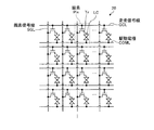
図8は、タッチ検出デバイス30の一構成例を斜視的に表す図である。タッチ検出デバイス30は、対向基板3に設けられた、駆動電極COMLおよびタッチ検出電極TDLにより構成されている。駆動電極COMLは、図の左右方向に延在する複数のストライプ状の電極パターンに分割されている。タッチ検出動作を行う際は、各電極パターンには、駆動電極ドライバ14によってタッチ検出駆動信号Vcomtが順次供給され、線順次走査駆動が行われるようになっている。タッチ検出電極TDLは、駆動電極COMLの電極パターンの延在方向と直交する方向に延びるストライプ状の電極パターンから構成されている。タッチ検出電極TDLの各電極パターンは、タッチ検出回路40のアナログLPF部42の入力にそれぞれ接続されている。駆動電極COMLとタッチ検出電極TDLにより互いに交差した電極パターンは、その交差部分に静電容量を形成している。
FIG. 8 is a perspective view illustrating a configuration example of the
この構成により、タッチ検出デバイス30では、タッチ検出動作を行う際、駆動電極ドライバ14が線順次走査するように駆動することにより、駆動電極COMLが順次選択され、タッチ検出電極TDLからタッチ検出信号Vdetを出力することにより、駆動電極COML毎のタッチ検出が行われるようになっている。つまり、駆動電極COMLは、図1〜図4に示したタッチ検出の基本原理における駆動電極E1に対応し、タッチ検出電極TDLは、図1〜図4に示したタッチ検出の基本原理におけるタッチ検出電極E2に対応するものであり、タッチ検出デバイス30はこの基本原理に従ってタッチを検出するようになっている。図8に示したように、互いに交差した電極パターンは、静電容量式タッチセンサをマトリックス状に構成している。よって、タッチ検出デバイス30のタッチ検出面全体にわたって走査することにより、外部近接物体の接触または近接が生じた位置の検出が可能となっている。
With this configuration, in the
次に、本実施形態に係るタッチ検出機能付き表示システムの概略構成及び各構成部における概略動作について説明する。図9は、実施形態1に係るタッチ検出機能付き表示システムの概略構成の一例を示す図である。 Next, a schematic configuration of the display system with a touch detection function according to the present embodiment and a schematic operation in each component will be described. FIG. 9 is a diagram illustrating an example of a schematic configuration of the display system with a touch detection function according to the first embodiment.
実施形態1に係るタッチ検出機能付き表示システム100は、図5に示したタッチ検出機能付き表示装置1と、タッチ検出デバイス30上の位置を指示する指示装置200とを備えている。なお、図9に示す例では、以降の説明を容易とするため、図5〜図8において説明した構成を一部置き換えている。図9に示す例において、タッチ制御回路300は、図5における駆動電極ドライバ14及びタッチ検出回路40を含み、表示制御回路400は、図5におけるゲートドライバ12及びソースドライバ13を含み、主制御回路500は、図5における制御部11を含むものとする。また、図9に示す例において、送信電極600は、図8における駆動電極COMLを示し、送信信号Txは、図5及び図8における駆動信号Vcomを示し、受信電極700は、図8におけるタッチ検出電極TDLを示し、受信信号Rxは、図5及び図8におけるタッチ検出信号Vdetを示している。なお、上述した図5〜図8に示す例では、駆動電極COMLには、表示動作を行う際には表示駆動信号Vcomdを供給するものとして説明したが、図9に示す例を用いる以下の説明では、表示動作を行う際の説明を省略する。
The display system with a
タッチ制御回路300、表示制御回路400、主制御回路500は、本発明における「制御回路」の一具体例に対応する。
The
本実施形態において、タッチ検出デバイス30は、上述したように、タッチ検出駆動信号Vcomt(ここでは、送信信号Tx)を、複数の駆動電極COML(ここでは、送信電極600)に時分割的に順次印加し、送信電極600に交差するタッチ検出電極TDL(ここでは、受信電極700)から出力されるタッチ検出信号Vdet(ここでは、受信信号Rx)を受信することによりタッチ検出動作を行うミューチュアル方式のタッチ検出デバイスである。図10は、本実施形態に係るタッチ検出機能付き表示システムにおいてタッチ制御回路から出力される送信信号Txの一例を示す図である。本実施形態において、タッチ制御回路300から出力される送信信号Txは、図10に示すように、波高値が等しい複数のパルスを含むパルス波形状の信号である。なお、図10に示す例では、送信信号Txのパルス数が8である場合を示したが、これに限るものではない。
In the present embodiment, as described above, the
図11は、実施形態1に係るタッチ検出機能付き表示システムにおける指示装置の一構成例を示す図である。指示装置200は、検出部201と、インターフェース部202と、コード付与部203と、反転回路204と、増幅回路205と、出力部206とを有する。コード付与部203、反転回路204、及び増幅回路205は、液晶表示デバイス20上における描画機能に対応した複数値のコードを含む生成信号ARxを生成する信号生成手段207として機能する。
FIG. 11 is a diagram illustrating a configuration example of an instruction device in the display system with a touch detection function according to the first embodiment. The
検出部201は、タッチ検出デバイス30に向けられる指示装置200の先端部分に形成される。そして、送信電極600に印加された送信信号Txの電位変動を検知し、検出送信信号Tdとしてコード付与部203に出力する。
The
インターフェース部202は、指示装置200によるタッチ検出デバイス30へのタッチ操作により液晶表示デバイス20上で実現したい描画機能をユーザーが設定するためのインターフェースである。
The interface unit 202 is an interface for the user to set a drawing function desired to be realized on the liquid
コード付与部203は、液晶表示デバイス20上で実現する描画機能に対応して、図10に示す送信信号Txを形成するパルスのうち、増幅率を下げるパルスが予め設定された複数のコードを保持している。
Corresponding to the drawing function realized on the liquid
図12は、液晶表示デバイス上で実現する描画機能、その描画機能に対応するコード、及び生成信号ARxの一例を示す図である。 FIG. 12 is a diagram illustrating an example of a drawing function realized on the liquid crystal display device, a code corresponding to the drawing function, and a generation signal ARx.
ここでは、液晶表示デバイス20上で実現する描画機能として、指示装置200のタッチ検出デバイス30上におけるタッチ検出位置に対応した液晶表示デバイス20上における軌跡で描画される線の色を選択する例について説明する。
Here, as a drawing function realized on the liquid
インターフェース部202は、例えば、カラーパレットを表示する簡易ディスプレイと色選択を行うためのインターフェースとを具備した構成とし、指示装置200のタッチ検出デバイス30上におけるタッチ検出位置に対応した液晶表示デバイス20上における軌跡の色を選択できるようにしてもよい。この場合、例えば、インターフェース部202から何れの色選択もなされていないと、コード付与部203は、描画機能「OFF」を示すコードが選択される。このとき、コード付与部203は、図10に示す送信信号Txにおける「1」のパルスの波高値のみ他のパルスよりも小さくしたコードを出力する。これにより、増幅回路205の出力である生成信号ARxの「1」のパルスの増幅率が他のパルスよりも小さくなる。
The interface unit 202 includes, for example, a simple display that displays a color palette and an interface for performing color selection, and is on the liquid
このように、描画機能として何も選択していない場合には、少なくとも生成信号ARxを形成する1のパルスの増幅率を小さくすることにより、タッチ検出回路40において検出したタッチ検出位置におけるタッチ操作が指示装置200によるものであることを示すことができる。
As described above, when nothing is selected as the drawing function, at least the amplification factor of one pulse forming the generation signal ARx is reduced, so that the touch operation at the touch detection position detected by the
また、例えば、インターフェース部202から「赤」を選択すると、描画機能「ペン色:赤」を示すコードが選択される。このとき、コード付与部203は、図10に示す送信信号Txにおける「1」、「3」、及び「4」のパルスの波高値を他のパルスよりも小さくした信号を出力する。これにより、増幅回路205の出力である生成信号ARxの「1」、「3」、及び「4」のパルスの増幅率が他のパルスよりも小さくなる。
For example, when “red” is selected from the interface unit 202, a code indicating the drawing function “pen color: red” is selected. At this time, the
また、例えば、インターフェース部202から「青」を選択すると、描画機能「ペン色:青」を示すコードが選択される。このとき、コード付与部203は、図10に示す送信信号Txにおける「1」、「5」、及び「6」のパルスの波高値を他のパルスよりも小さくした信号を出力する。これにより、増幅回路205の出力である生成信号ARxの「1」、「5」、及び「6」のパルスの増幅率が他のパルスよりも小さくなる。
For example, when “blue” is selected from the interface unit 202, a code indicating the drawing function “pen color: blue” is selected. At this time, the
ここで、図10乃至図13を参照して、信号生成手段207によって生成される生成信号ARxの生成手法の具体例について説明する。図13は、実施形態1に係るコード付与部の一構成例を示す図である。
Here, with reference to FIGS. 10 to 13, a specific example of a method for generating the generation signal ARx generated by the
コード付与部203は、検出部201から検出送信信号Tdが入力されると、検出送信信号Tdの各パルス、すなわち、図10に示す送信信号Txの「1」〜「8」の各パルスに同期して、インターフェース部202により選択された描画機能に対応した多値(ここでは、3値)のパルス信号を生成する。
When the detection transmission signal Td is input from the
図13に示すように、コード付与部203は、複数のコードを保持したコード保持部2031と、生成するパルス信号に応じた複数値(ここでは、3値)の電圧レベルを出力する電圧付与部2032を有している。コード保持部2031は、インターフェース部202により選択された描画機能毎に対応したコードを電圧付与部2032に出力する。電圧付与部2032は、検出送信信号Tdの1つ目のパルス、すなわち、図10に示す送信信号Txの「1」のパルスをトリガーとして、送信信号Txの「1」〜「8」の各パルス毎に、コード保持部2031から出力されたコードに応じた電圧レベルを選択する。これにより、インターフェース部202で選択されたコードに対応した多値(ここでは、3値)のパルス信号が生成される。なお、電圧付与部2032は、各電圧レベルを出力する複数の電源回路で構成されていてもよいし、各電圧レベルを選択可能な1つの電源回路であってもよい。
As illustrated in FIG. 13, the
反転回路204は、コード付与部203で生成されたパルス信号を反転させる。増幅回路205は、反転回路204で反転されたパルス信号を予め定められた所定の増幅率で増幅する。上記のようにして、インターフェース部202で選択された描画機能に対応したコードを含む生成信号ARx(図12)が生成される。
The inverting
出力部206は、検出部201と同様に、指示装置200の先端部分に形成される。そして、信号生成手段207によって生成された生成信号ARxを、指示装置200の先端部分と送信電極600との間に形成される静電容量(図1〜図4に示したタッチ検出の基本原理におけるC2’に相当)を介して、送信電極600と受信電極700との交差部分に出力する。これにより、後段のタッチ制御回路300に入力される受信信号Rxには、信号生成手段207によって生成された生成信号ARxが重畳する。このように、受信信号Rxに生成信号ARxが重畳されることで、指示装置200の先端部分と送信電極600との間に形成される静電容量(図1〜図4に示したタッチ検出の基本原理におけるC2’に相当)が小さい場合でも、指示装置200によるタッチ状態の検出精度を高めることができる。
The
図14は、実施形態1に係るタッチ検出機能付き表示システムにおけるタッチ制御回路の一構成例を示す図である。タッチ制御回路300は、図5に示す駆動電極ドライバ14及びタッチ検出回路40に加えて、コード識別部301及び機能選択部302を備えている。なお、図14に示す例では、駆動電極ドライバ14を省略している。
FIG. 14 is a diagram illustrating a configuration example of a touch control circuit in the display system with a touch detection function according to the first embodiment. The
タッチ検出回路40及びコード識別部301には、生成信号ARxが重畳された受信信号Rxが入力される。
A reception signal Rx on which the generation signal ARx is superimposed is input to the
コード識別部301は、受信信号Rxを解析し、受信信号Rxに重畳された生成信号ARxに含まれるコードを識別する。機能選択部302は、予め設定された複数の描画機能に対応したコードを保持している。機能選択部302は、コード識別部301によって識別されたコードに対応する描画機能を選択して、描画機能情報を出力する。なお、コード識別部301によりコードが含まれていないものとして識別された場合、すなわち、受信信号Rxを構成するパルスが全て同値であることが検出された場合には、機能選択部302は、描画機能情報を出力しない。
The
タッチ検出回路40から出力されたタッチ検出位置情報及び描画機能情報は、主制御回路500に入力される。主制御回路500は、タッチ検出回路40から出力されたタッチ検出位置情報及び描画機能情報に基づき、タッチ検出デバイス30上におけるタッチ検出位置に対応した液晶表示デバイス20上における位置において、指示装置200のインターフェース部202で選択された描画機能を実現するための制御信号を、表示制御回路400に出力する。
Touch detection position information and drawing function information output from the
なお、タッチ制御回路300から描画機能情報が出力されず、タッチ検出位置情報のみが出力された場合には、主制御回路500は、タッチ操作を行った物体が、例えば、ユーザーの指等の指示装置200以外の物であるものとして処理する。この場合には、例えば、タッチ検出デバイス30上におけるタッチ検出位置に対応した液晶表示デバイス20上における位置に表示されたオブジェクトの選択や移動等を行うものとして処理する。
If the drawing function information is not output from the
また、例えば、指示装置200でのタッチ操作を行っている際にユーザーの指等の指示装置200以外の物体によるタッチ操作を許容していない場合に、複数箇所でタッチ検出され、1つのタッチ検出位置が指示装置200によるものであると判定した場合には、主制御回路500は、指示装置200によりタッチ検出された位置以外へのタッチ操作をリジェクトする。すなわち、いわゆるパームリジェクション機能を実現することができる。
Further, for example, when a touch operation with the object other than the
また、指示装置200のインターフェース部202で選択された描画機能が「OFF」である場合には、主制御回路500は、タッチ操作を行った物体が、例えば、ユーザーの指等の指示装置200以外の物である場合と同様の処理、例えば、タッチ検出デバイス30上におけるタッチ検出位置に対応した液晶表示デバイス20上における位置に表示されたオブジェクトの選択や移動等を行うものとして処理する。
When the drawing function selected by the interface unit 202 of the
次に、実施形態1に係るタッチ検出機能付き表示システム100における具体的な処理フローについて説明する。図15は、実施形態1に係るタッチ検出機能付き表示システムにおける具体的な処理フローの一例を示す図である。
Next, a specific processing flow in the display system with a
タッチ制御回路300は、タッチ検出期間において、複数の送信電極600に対し、時分割で送信信号Txを出力し(ステップS1)、複数の受信電極700から受信信号Rxが入力される(ステップS2)。
In the touch detection period, the
タッチ制御回路300は、複数の受信電極700から入力される受信信号Rxを監視し、タッチ検出回路40によりタッチ操作が検出されると(ステップS3)、タッチ検出回路40からタッチ検出位置情報を主制御回路500に出力する(ステップS4)。そして、コード識別部301は、受信信号Rxにコードが含まれているか否かを識別する(ステップS5)。
The
受信信号Rxにコードが含まれている場合(ステップS5;Yes)、コード識別部301は、受信信号Rxに含まれるコードを識別し(ステップS6)、機能選択部302は、コード識別部301により識別されたコードに対応した描画機能を選択して(ステップS7)、主制御回路500に描画機能情報を出力する(ステップS8)。
When the received signal Rx includes a code (step S5; Yes), the
主制御回路500は、タッチ制御回路300から出力されたタッチ検出位置情報及び描画機能情報に基づき、指示装置200によりタッチ操作が行われたものとして判定する(ステップS9)。そして、主制御回路500は、タッチ検出デバイス30上におけるタッチ検出位置に対応した液晶表示デバイス20上における位置において、指示装置200のインターフェース部202で選択された描画機能を実現するための制御信号を表示制御回路400に出力し(ステップS10)、本処理フローを終了する。
The
受信信号Rxにコードが含まれていない場合(ステップS5;No)、タッチ制御回路300は、主制御回路500に描画機能情報を出力しない。これにより、主制御回路500は、タッチ操作を行った物体が、例えば、ユーザーの指等の指示装置200以外の物であるものと判定する(ステップS11)。そして、主制御回路500は、ユーザーの指等の指示装置200以外の物によるタッチ操作に応じた処理(例えば、タッチ検出デバイス30上におけるタッチ検出位置に対応した液晶表示デバイス20上における位置に表示されたオブジェクトの選択や移動等)を行わせるための制御信号を表示制御回路400に出力し(ステップS10)、本処理フローを終了する。
When the received signal Rx does not include a code (step S5; No), the
上記した処理フローを実施することにより、指示装置200のインターフェース部202で選択された描画機能が液晶表示デバイス20上で実現される。
By performing the processing flow described above, the drawing function selected by the interface unit 202 of the
なお、上述した例では、液晶表示デバイス20上で実現する描画機能として、指示装置200のタッチ検出デバイス30上におけるタッチ検出位置に対応した液晶表示デバイス20上における軌跡で描画される線の色を選択する例について説明したが、液晶表示デバイス20上で実現する描画機能としてはこれに限らず、例えば、液晶表示デバイス20上における指示装置200の軌跡で描画される線の太さや線種等を選択するようにしてもよい。また、液晶表示デバイス20上に表示されたオブジェクトを、液晶表示デバイス20上における指示装置200の軌跡により消去する消しゴム機能を選択するようにしてもよい。
In the above-described example, as a drawing function realized on the liquid
また、上述した例では、指示装置200によるタッチ操作であることを示すために、図12の描画機能「OFF」を示すコードを、図10に示す送信信号Txにおける「1」のパルスの増幅率を他のパルスよりも小さくした例について説明したが、例えば、送信信号Txを構成するパルスのうちの複数のパルスを用いて、複数本の指示装置200に対応する識別コードを形成するようにしてもよい。このようにすれば、複数本の指示装置200を用いる構成とすることも可能である。
In the example described above, the code indicating the drawing function “OFF” in FIG. 12 is used as the amplification factor of the pulse “1” in the transmission signal Tx shown in FIG. However, for example, an identification code corresponding to a plurality of
また、上述した例では、図12に示すような3値のコードを含む生成信号ARxを生成する例を示したが、これに限らず、2値あるいは4値以上の複数値のコードを含む生成信号ARxを生成するようにしてもよい。このようにすれば、より多くの情報を受信信号Rxに重畳して送信することができ、多様な描画機能が実現可能となる。 In the above-described example, the generation signal ARx including the ternary code as illustrated in FIG. 12 is illustrated. However, the generation signal ARx is not limited to this, and the generation includes a binary code or a multi-value code of four or more values. The signal ARx may be generated. In this way, more information can be transmitted superimposed on the received signal Rx, and various drawing functions can be realized.
以上説明したように、実施形態1に係るタッチ検出機能付き表示システムによれば、指示装置200は、タッチ制御回路300から出力される波高値が等しい複数のパルスを含む送信信号Txを送信電極600から検出し、送信信号Txを形成する複数のパルスのうち、いくつかのパルスの増幅率を他のパルスの増幅率と異ならせて反転増幅することで、予め設定した液晶表示デバイス20上における複数種の描画機能のうち、指示装置200に具備されたインターフェース部202で選択した描画機能に対応した2値以上のコードを含む生成信号ARxを生成し、指示装置200が指し示したタッチ検出デバイス30上に位置する受信電極700に対して出力する。タッチ制御回路300は、受信信号Rxに含まれるコードを識別し、当該コードに対応した描画機能を選択する。そして、主制御回路500は、タッチ検出デバイス30上におけるタッチ検出位置に対応した液晶表示デバイス20上における位置において、タッチ制御回路300により選択された描画機能を実現するための制御信号を表示制御回路400に出力する。これにより、液晶表示デバイス20上における指示装置200の位置において、指示装置200で選択した描画機能を実現することができる。
As described above, according to the display system with a touch detection function according to the first embodiment, the
また、何れの描画機能も選択していない場合には、送信信号Txを形成する複数のパルスのうち、少なくとも1のパルスの増幅率を他のパルスの増幅率と異ならせて生成信号ARxを生成することにより、タッチ検出回路40において検出したタッチ検出位置におけるタッチ操作が指示装置200によるものであることを示すことができる。これにより、タッチ操作を行った物体が、ユーザーの指等の指示装置200以外の物である場合と区別することができ、指示装置200でのタッチ操作を行っている際にユーザーの指等の指示装置200以外の物体によるタッチ操作を許容していない場合に、複数箇所でタッチ検出され、1つのタッチ検出位置が指示装置200によるものであると判定した場合には、指示装置200によりタッチ検出された位置以外へのタッチ操作をリジェクトすることができ、いわゆるパームリジェクション機能を実現することができる。
When no drawing function is selected, the generation signal ARx is generated by making the amplification factor of at least one pulse different from the amplification factors of other pulses among the plurality of pulses forming the transmission signal Tx. By doing so, it can be shown that the touch operation at the touch detection position detected by the
また、コードを3値以上とすることで、より多くの情報を受信信号Rxに重畳して送信することができ、多様な描画機能が実現できる。 Further, by setting the code to three or more values, more information can be transmitted by being superimposed on the received signal Rx, and various drawing functions can be realized.
また、送信信号Txを構成するパルスのうちの複数のパルスを用いて、複数本の指示装置200に対応する識別コードを形成するようにすれば、複数本の指示装置200を用いる構成とすることもできる。
Further, if an identification code corresponding to a plurality of
また、受信信号Rxに生成信号ARxが重畳されることで、指示装置200の先端部分と送信電極600との間に形成される静電容量が小さい場合でも、指示装置200によるタッチ状態の検出精度を高めることができる。
In addition, since the generation signal ARx is superimposed on the reception signal Rx, even when the capacitance formed between the distal end portion of the
本実施形態により、複数種の機能を持たせた1つの指示装置200の各種機能を、タッチ操作のみで実現可能なタッチ検出機能付き表示システム100を提供することができる。
According to the present embodiment, it is possible to provide the
(実施形態2)
図16は、実施形態2に係るタッチ検出機能付き表示システムにおける指示装置の一構成例を示す図である。なお、上述した実施形態で説明したものと同じ構成要素には同一の符号を付して重複する説明は省略する。
(Embodiment 2)
FIG. 16 is a diagram illustrating a configuration example of an instruction device in the display system with a touch detection function according to the second embodiment. Note that the same components as those described in the above-described embodiment are denoted by the same reference numerals, and redundant description is omitted.
本実施形態では、図11に示した実施形態1におけるインターフェース部202に代えて、指示装置200aの先端部に圧力センサー208を具備した構成としている。これにより、液晶表示デバイス20上で実現する描画機能として、例えば、液晶表示デバイス20上における指示装置200の軌跡の線の濃淡を筆圧に応じて変化させるような描画機能を実現することができる。
In this embodiment, instead of the interface unit 202 in the first embodiment shown in FIG. 11, a
図16に示す信号生成手段207によって生成される生成信号ARxの生成手法については、上述した実施形態1と同様である。図17は、実施形態2に係るコード付与部の一構成例を示す図である。以下、図16及び図17を参照して、実施形態2における生成信号ARxの生成手法について説明する。
The generation method of the generation signal ARx generated by the
コード付与部203aは、検出部201から検出送信信号Tdが入力されると、検出送信信号Tdの各パルス、すなわち、送信信号Txの「1」〜「8」の各パルスに同期して、圧力センサー208により検知される筆圧に対応した多値(例えば、3値)のパルス信号を生成する。
When the detection transmission signal Td is input from the
図17に示すように、コード付与部203aは、複数のコードを保持したコード保持部2031aと、生成するパルス信号に応じた複数値(例えば、3値)の電圧レベルを出力する電圧付与部2032aを有している。コード保持部2031aは、圧力センサー208により検知される筆圧毎に対応したコードを電圧付与部2032aに出力する。電圧付与部2032aは、検出送信信号Tdの1つ目のパルス、すなわち、送信信号Txの「1」のパルスをトリガーとして、送信信号Txの「1」〜「8」の各パルス毎に、コード保持部2031aから出力されたコードに応じた電圧レベルを選択する。これにより、圧力センサー208により検知された筆圧に対応した多値(例えば、3値)のパルス信号が生成される。なお、電圧付与部2032aは、各電圧レベルを出力する複数の電源回路で構成されていてもよいし、各電圧レベルを選択可能な1つの電源回路であってもよい。
As illustrated in FIG. 17, the code applying unit 203a includes a code holding unit 2031a that stores a plurality of codes, and a
反転回路204は、コード付与部203で生成されたパルス信号を反転させる。増幅回路205は、反転回路204で反転されたパルス信号を予め定められた所定の増幅率で増幅する。上記のようにして、圧力センサー208により検知された筆圧に対応したコードを含む生成信号ARxが生成される。
The inverting
出力部206は、検出部201と同様に、指示装置200aの先端部分に形成される。そして、信号生成手段207によって生成された生成信号ARxを、指示装置200aの先端部分と送信電極600との間に形成される静電容量(図1〜図4に示したタッチ検出の基本原理におけるC2’に相当)を介して、送信電極600と受信電極700との交差部分に出力する。これにより、後段のタッチ制御回路300に入力される受信信号Rxには、信号生成手段207によって生成された生成信号ARxが重畳する。このように、受信信号Rxに生成信号ARxが重畳されることで、指示装置200aの先端部分と送信電極600との間に形成される静電容量(図1〜図4に示したタッチ検出の基本原理におけるC2’に相当)が小さい場合でも、指示装置200aによるタッチ状態の検出精度を高めることができる。
Similar to the
なお、図16に示す例では、図11に示した実施形態1におけるインターフェース部202に代えて、指示装置200aの先端部に圧力センサー208を具備した構成を示したが、圧力センサー208に加えてインターフェース部202を具備した構成としてもよいことは言うまでもない。
In the example illustrated in FIG. 16, a configuration in which the
以上説明したように、実施形態2に係るタッチ検出機能付き表示システムによれば、指示装置200aの先端部に圧力センサー208を具備した構成とすることで、例えば、液晶表示デバイス20上における指示装置200aの軌跡の線の濃淡を筆圧に応じて変化させるような描画機能を実現することができる。
As described above, according to the display system with a touch detection function according to the second embodiment, for example, the indication device on the liquid
また、圧力センサー208に加えてインターフェース部202を具備した構成とすることで、実施形態1よりも多様な描画機能を実現することができる。
Further, by adopting a configuration in which the interface unit 202 is provided in addition to the
(実施形態3)
図18は、実施形態3に係るタッチ検出機能付き表示システムにおける指示装置の一構成例を示す図である。なお、上述した実施形態で説明したものと同じ構成要素には同一の符号を付して重複する説明は省略する。
(Embodiment 3)
FIG. 18 is a diagram illustrating a configuration example of an instruction device in the display system with a touch detection function according to the third embodiment. Note that the same components as those described in the above-described embodiment are denoted by the same reference numerals, and redundant description is omitted.
本実施形態では、図11に示した実施形態1におけるインターフェース部202、及び、図16に示した圧力センサー208に代えて、指示装置200bの傾きを検出する傾きセンサー209を具備した構成としている。これにより、液晶表示デバイス20上で実現する描画機能として、例えば、液晶表示デバイス20上における指示装置200bの軌跡の線の太さを指示装置200bの傾きに応じて変化させるような描画機能を実現することができる。
In this embodiment, instead of the interface unit 202 in the first embodiment shown in FIG. 11 and the
図18に示す信号生成手段207によって生成される生成信号ARxの生成手法については、上述した実施形態1,2と同様である。図19は、実施形態3に係るコード付与部の一構成例を示す図である。以下、図18及び図19を参照して、実施形態3における生成信号ARxの生成手法について説明する。
The generation method of the generation signal ARx generated by the
コード付与部203bは、検出部201から検出送信信号Tdが入力されると、検出送信信号Tdの各パルス、すなわち、送信信号Txの「1」〜「8」の各パルスに同期して、傾きセンサー209により検知される指示装置200bの傾きに対応した多値(例えば、3値)のパルス信号を生成する。
When the detection transmission signal Td is input from the
図19に示すように、コード付与部203bは、複数のコードを保持したコード保持部2031bと、生成するパルス信号に応じた複数値(例えば、3値)の電圧レベルを出力する電圧付与部2032bを有している。コード保持部2031bは、傾きセンサー209により検知される指示装置200bの傾き毎に対応したコードを電圧付与部2032bに出力する。電圧付与部2032bは、検出送信信号Tdの1つ目のパルス、すなわち、送信信号Txの「1」のパルスをトリガーとして、送信信号Txの「1」〜「8」の各パルス毎に、コード保持部2031aから出力されたコードに応じた電圧レベルを選択する。これにより、傾きセンサー209により検知された指示装置200bの傾きに対応した多値(例えば、3値)のパルス信号が生成される。なお、電圧付与部2032bは、各電圧レベルを出力する複数の電源回路で構成されていてもよいし、各電圧レベルを選択可能な1つの電源回路であってもよい。
As illustrated in FIG. 19, the
反転回路204は、コード付与部203で生成されたパルス信号を反転させる。増幅回路205は、反転回路204で反転されたパルス信号を予め定められた所定の増幅率で増幅する。上記のようにして、傾きセンサー209により検知された指示装置200bの傾きに対応したコードを含む生成信号ARxが生成される。
The inverting
出力部206は、検出部201と同様に、指示装置200bの先端部分に形成される。そして、信号生成手段207によって生成された生成信号ARxを、指示装置200bの先端部分と送信電極600との間に形成される静電容量(図1〜図4に示したタッチ検出の基本原理におけるC2’に相当)を介して、送信電極600と受信電極700との交差部分に出力する。これにより、後段のタッチ制御回路300に入力される受信信号Rxには、信号生成手段207によって生成された生成信号ARxが重畳する。このように、受信信号Rxに生成信号ARxが重畳されることで、指示装置200bの先端部分と送信電極600との間に形成される静電容量(図1〜図4に示したタッチ検出の基本原理におけるC2’に相当)が小さい場合でも、指示装置200bによるタッチ状態の検出精度を高めることができる。
Similar to the
なお、図18に示す例では、図11に示した実施形態1におけるインターフェース部202、及び、図16に示した圧力センサー208に代えて、指示装置200bの傾きを検出する傾きセンサー209を具備した構成を示したが、傾きセンサー209に加えてインターフェース部202と圧力センサー208との一方あるいは双方を具備した構成としてもよいことは言うまでもない。
18 includes an
以上説明したように、実施形態3に係るタッチ検出機能付き表示システムによれば、指示装置200bの傾きを検出する傾きセンサー209を具備した構成とすることで、例えば、液晶表示デバイス20上における指示装置200bの軌跡の線の太さを指示装置200bの傾きに応じて変化させるような描画機能を実現することができる。
As described above, according to the display system with a touch detection function according to the third embodiment, for example, an instruction on the liquid
また、傾きセンサー209に加えてインターフェース部202と圧力センサー208との一方あるいは双方を具備した構成とすることで、実施形態1あるいは実施形態2よりも多様な描画機能を実現することができる。
In addition to the
(実施形態4)
図20は、実施形態4に係るタッチ検出機能付き表示システムの概略構成の一例を示す図である。また、図21は、実施形態4に係るタッチ検出機能付き表示システムにおける指示装置の一構成例を示す図である。なお、上述した実施形態で説明したものと同じ構成要素には同一の符号を付して重複する説明は省略する。
(Embodiment 4)
FIG. 20 is a diagram illustrating an example of a schematic configuration of a display system with a touch detection function according to the fourth embodiment. FIG. 21 is a diagram illustrating a configuration example of an instruction device in the display system with a touch detection function according to the fourth embodiment. Note that the same components as those described in the above-described embodiment are denoted by the same reference numerals, and redundant description is omitted.
上述した実施形態1乃至3では、タッチ検出デバイス30として、送信電極600と受信電極700との交差部分の静電容量の変化に基づいてタッチ位置を検出するミューチュアル方式のタッチ検出デバイスを用いた例について説明したが、本実施形態では、図20に示すように、タッチ検出デバイス30aとして、互いに交差する受信電極700a,700bと検出対象である指示装置200cとの間の静電容量の変化に基づいてタッチ位置を検出するセルフ方式のタッチ検出デバイスを用いている。
In the first to third embodiments described above, an example in which the
本実施形態に係るタッチ検出機能付き表示システム100aにおいて、タッチ検出デバイス30aは、一方向に延在するように併設された複数の受信電極700aと、この受信電極700aと交差する方向に延在するように併設された複数の受信電極700bを有している。
In the display system with a
タッチ制御回路300aには、受信電極700aからの受信信号Rx1と、受信電極700bからの受信信号Rx2との双方が入力される。
Both the reception signal Rx1 from the
指示装置200cは、インターフェース部202と、コード付与信号生成部203aと、反転回路204と、増幅回路205と、出力部206とを有する。コード付与信号生成部208、反転回路204、及び増幅回路205は、信号生成手段207aとして機能する。
The
コード付与信号生成部208は、液晶表示デバイス20上で実現する描画機能に対応した複数のコードを保持している。
The code giving
コード付与信号生成部208は、インターフェース部202で選択された描画機能に対応したコードを付与した信号を出力する。そして、その信号は、後段の反転回路204及び増幅回路205で反転増幅され、生成信号ARxが生成される。
The code addition
図21に示す信号生成手段207aによって生成される生成信号ARxの生成手法については、上述した実施形態1乃至3とは一部異なる。図22は、実施形態4に係るコード付与信号生成部の一構成例を示す図である。以下、図21及び図22を参照して、実施形態3における生成信号ARxの生成手法について説明する。
The generation method of the generation signal ARx generated by the
コード付与信号生成部208は、インターフェース部202により選択されるコードに対応した多値(例えば、3値)のパルス信号を生成する。
The code giving
図22に示すように、コード付与信号生成部208は、例えば、パルス信号生成部2081と、生成するパルス信号に応じた複数値(例えば、3値)の電圧レベルを出力する電圧付与部2082と、を有している。パルス信号生成部2081は、インターフェース部202により選択された描画機能毎に対応したコードを付与した信号と、このコードの前にコードの先頭を示す予め定められたヘッダパターンを付与して電圧付与部2082に出力する。なお、描画機能毎のコードには、ヘッダパターンと一致するパターンが含まれないものとする。これにより、後述するタッチ制御回路300aにおいてヘッダパターンを検出できる。
As illustrated in FIG. 22, the code application
電圧付与部2082は、パルス信号生成部2081で生成されるパルス信号の1つ目のパルスをトリガーとして、当該パルス信号の各パルス毎に、パルス信号生成部2081から出力されたコードに応じた電圧レベルを選択する。これにより、インターフェース部202で選択されたコードに対応した多値(ここでは、3値)のパルス信号が生成される。なお、電圧付与部2082は、各電圧レベルを出力する複数の電源回路で構成されていてもよいし、各電圧レベルを選択可能な1つの電源回路であってもよい。
The
反転回路204は、コード付与信号生成部208で生成されたパルス信号を反転させる。増幅回路205は、反転回路204で反転されたパルス信号を予め定められた所定の増幅率で増幅する。上記のようにして、インターフェース部202で選択された描画機能に対応したコードと予め定められたヘッダパターンとを含む生成信号ARxが生成される。
The
出力部206は、指示装置200cの先端部分に形成される。そして、信号生成手段207aによって生成された生成信号ARxを、指示装置200cの先端部分と受信電極700a及び受信電極700bとの間に形成される静電容量を介して、受信電極700aと受信電極700bとの交差部分に出力する。これにより、後段のタッチ制御回路300aに入力される受信信号Rx1,Rx2は、信号生成手段207aによって生成された生成信号ARxが重畳した波形となり、指示装置200cの先端部分と受信電極700a及び受信電極700bとの間に形成される静電容量が小さい場合でも、指示装置200cによるタッチ状態の検出精度を高めることができる。
The
なお、図21に示す例では、反転回路204を具備した構成を記載したが、本実施形態に係るセルフ方式のタッチ検出デバイスを用いた場合には、反転回路204を具備しない構成であってもよい。この反転回路204の有無により、本発明が限定されるものではない。
In the example shown in FIG. 21, the configuration including the
図23は、実施形態4に係るタッチ検出機能付き表示システムにおけるタッチ制御回路の一構成例を示す図である。タッチ制御回路300aは、タッチ検出回路40a、コード識別部301a、コード識別部301b、及び機能選択部302aを備えている。
FIG. 23 is a diagram illustrating a configuration example of a touch control circuit in the display system with a touch detection function according to the fourth embodiment. The touch control circuit 300a includes a
タッチ検出回路40aは、受信信号Rx1と受信信号Rx2とが入力されてタッチ検出位置情報を出力する。
The
コード識別部301aは、受信信号Rx1に含まれるヘッダパターンを検出した場合に、そのヘッダパターンに続くコードを識別する。コード識別部301bは、受信信号Rx2に含まれるヘッダパターンを検出した場合に、そのヘッダパターンに続くコードを識別する。機能選択部302aは、予め設定された複数の描画機能に対応したコードを保持している。機能選択部302aは、コード識別部301aとコード識別部301bとで一致したコードに対応する描画機能を選択して、描画機能情報を出力する。以降の主制御回路500、及び表示制御回路400における動作は、上述した実施形態1乃至3と同様である。
When the
なお、上述した例では、実施形態1と同様に、指示装置200cがインターフェース部202を具備した構成を示したが、実施形態2と同様に、インターフェース部202に代えて、指示装置200cの先端部に圧力センサーを具備した構成、あるいは、インターフェース部202と圧力センサーとを具備した構成であってもよいし、実施形態3と同様に、インターフェース部202に代えて、指示装置200cの傾きを検出する傾きセンサーを具備した構成、インターフェース部202と傾きセンサーとを具備した構成、あるいは、インターフェース部202と圧力センサーと傾きセンサーとを具備した構成であってもよい。
In the above-described example, the configuration in which the
以上説明したように、実施形態4に係るタッチ検出機能付き表示システムによれば、タッチ検出デバイス30aがセルフ方式のタッチ検出デバイスである場合でも、指示装置200cにおいて各種描画機能に対応したコードを含む生成信号ARxを出力することで、実施形態1乃至3において説明したミューチュアル方式のタッチ検出デバイスの場合と同様に、複数種の機能を持たせた1つの指示装置200cの各種機能を、タッチ操作のみで実現可能なタッチ検出機能付き表示システム100aを提供することができる。
As described above, according to the display system with a touch detection function according to the fourth embodiment, even when the
以上、実施形態について説明したが、上述した各実施形態の構成を組み合わせることも可能であり、上述した内容により本発明が限定されるものではない。また、上述した本発明の構成要素には、当業者が容易に想定できるもの、実質的に同一のもの、いわゆる均等の範囲のものが含まれる。さらに、上述した構成要素は適宜組み合わせることが可能である。また、本発明の要旨を逸脱しない範囲で構成要素の種々の省略、置換及び変更を行うことができる。 Although the embodiments have been described above, the configurations of the above-described embodiments can be combined, and the present invention is not limited by the above-described contents. The above-described constituent elements of the present invention include those that can be easily assumed by those skilled in the art, those that are substantially the same, and those in a so-called equivalent range. Furthermore, the above-described components can be appropriately combined. In addition, various omissions, substitutions, and changes of the components can be made without departing from the scope of the present invention.
1,1a タッチ検出機能付き表示装置
2 画素基板
3 対向基板
6 液晶層
10 タッチ検出機能付き表示デバイス
11 制御部
12 ゲートドライバ
13 ソースドライバ
14 駆動電極ドライバ
20 液晶表示デバイス
21 TFT基板
22 画素電極
30,30a タッチ検出デバイス
31 ガラス基板
32 カラーフィルタ
35 偏光板
40,40a タッチ検出回路
42 アナログLPF部
43 A/D変換部
44 信号処理部
45 座標抽出部
46 検出タイミング制御部
100,100a タッチ検出機能付き表示システム
200,200a,200b,200c 指示装置
201 検出部
202 インターフェース部
203,203a,203b コード付与部
204 反転回路
205 増幅回路
206 出力部
207,207a 信号生成手段
208 コード付与信号生成部
300,300a タッチ制御回路
301,301a,301b コード識別部
302,302a 機能選択部
400 表示制御回路
500 主制御回路
600 送信電極
700,700a,700b 受信電極
2031,2031a,2031b コード保持部
2032,2032a,2032b 電圧付与部
2081 パルス信号生成部
2082 電圧付与部
DESCRIPTION OF
Claims (8)
前記タッチ検出デバイス上の位置を指示する指示装置と、
を備え、
前記指示装置は、
予め設定した前記表示デバイス上における複数の描画機能に対応した2値以上の複数のコードを保持し、前記送信電極から前記送信信号を検出して、前記コードに基づき、前記複数のパルスのうち少なくとも1のパルスの増幅率を他のパルスの増幅率と異ならせて反転増幅して生成した生成信号を前記受信電極に対して出力し、
前記制御回路は、
前記生成信号に含まれる前記コードを識別し、当該コードに対応した前記描画機能を、前記表示デバイス上における前記指示装置の位置で実現する、
タッチ検出機能付き表示システム。 A display device and a plurality of transmission electrodes provided so as to extend in one direction, and a capacitance formed between the display device and the transmission electrodes provided so as to extend in a direction intersecting with the transmission electrode. A touch detection device provided opposite to the display device, and a transmission signal including a plurality of pulses having the same peak value to the transmission electrode, and receiving from the reception electrode A display device with a touch detection function comprising: a control circuit that detects at least a position of the pointing device on the touch detection device based on a signal and displays the position on the display device;
An indicating device for indicating a position on the touch detection device;
With
The pointing device is
Holding a plurality of binary codes corresponding to a plurality of drawing functions on the display device set in advance, detecting the transmission signal from the transmission electrode, and based on the code, at least of the plurality of pulses A generated signal generated by inverting and amplifying one pulse with a different amplification factor from another pulse is output to the receiving electrode,
The control circuit includes:
Identifying the code included in the generated signal, and realizing the drawing function corresponding to the code at a position of the pointing device on the display device;
Display system with touch detection function.
請求項1に記載のタッチ検出機能付き表示システム。 The pointing device includes an interface unit for setting a plurality of the drawing functions in the pointing device.
The display system with a touch detection function according to claim 1.
請求項1又は請求項2に記載のタッチ検出機能付き表示システム。 The pointing device includes, as the drawing function, a color of a line drawn by a locus of the pointing device on the display device corresponding to a touch detection position on the touch detection device,
The display system with a touch detection function according to claim 1 or 2.
請求項1乃至請求項3の何れか一項に記載のタッチ検出機能付き表示システム。 The pointing device includes, as the drawing function, a thickness of a line drawn by a locus of the pointing device on the display device corresponding to a touch detection position on the touch detection device.
The display system with a touch detection function according to any one of claims 1 to 3.
請求項1乃至請求項4の何れか一項に記載のタッチ検出機能付き表示システム。 The pointing device includes, as the drawing function, a function of erasing an object displayed on the display device by a locus of the pointing device on the display device corresponding to a touch detection position on the touch detection device.
The display system with a touch detection function according to any one of claims 1 to 4.
請求項1乃至請求項5の何れか一項に記載のタッチ検出機能付き表示システム。 The pointing device includes a pressure sensor that detects a pressure between the pointing device and the touch detection device, and the touch detection device according to a magnitude of pressure detected by the pressure sensor as the drawing function. Including a function of changing the shading of a line drawn by the locus of the pointing device on the display device corresponding to the touch detection position on the display device;
The display system with a touch detection function according to any one of claims 1 to 5.
請求項1乃至請求項6の何れか一項に記載のタッチ検出機能付き表示システム。 The pointing device includes a tilt sensor that detects a tilt of the pointing device on the display device, and the drawing function has a touch detection position on the touch detection device according to the tilt detected by the tilt sensor. Including a function of changing a thickness of a line drawn on a locus of the pointing device on the corresponding display device;
The display system with a touch detection function according to any one of claims 1 to 6.
請求項1乃至請求項7の何れか一項に記載のタッチ検出機能付き表示システム。 Forming a plurality of identification codes corresponding to a plurality of the indicating devices with a plurality of pulses constituting the generated signal;
The display system with a touch detection function according to any one of claims 1 to 7.
Priority Applications (3)
| Application Number | Priority Date | Filing Date | Title |
|---|---|---|---|
| JP2015112348A JP2016224808A (en) | 2015-06-02 | 2015-06-02 | Display system with touch detection function |
| US15/161,758 US20160357292A1 (en) | 2015-06-02 | 2016-05-23 | Display system with touch detection function |
| US15/959,652 US20180239479A1 (en) | 2015-06-02 | 2018-04-23 | Display system with touch detection function |
Applications Claiming Priority (1)
| Application Number | Priority Date | Filing Date | Title |
|---|---|---|---|
| JP2015112348A JP2016224808A (en) | 2015-06-02 | 2015-06-02 | Display system with touch detection function |
Publications (1)
| Publication Number | Publication Date |
|---|---|
| JP2016224808A true JP2016224808A (en) | 2016-12-28 |
Family
ID=57451032
Family Applications (1)
| Application Number | Title | Priority Date | Filing Date |
|---|---|---|---|
| JP2015112348A Pending JP2016224808A (en) | 2015-06-02 | 2015-06-02 | Display system with touch detection function |
Country Status (2)
| Country | Link |
|---|---|
| US (2) | US20160357292A1 (en) |
| JP (1) | JP2016224808A (en) |
Cited By (4)
| Publication number | Priority date | Publication date | Assignee | Title |
|---|---|---|---|---|
| WO2018163972A1 (en) * | 2017-03-07 | 2018-09-13 | シャープ株式会社 | Touch panel and electronic device |
| US10732447B2 (en) | 2017-03-07 | 2020-08-04 | Sharp Kabushiki Kaisha | Touch panel and electronic device |
| JP2021132319A (en) * | 2020-02-20 | 2021-09-09 | 株式会社セガ | Amusement imaging equipment and programs |
| CN115712357A (en) * | 2020-03-10 | 2023-02-24 | 深圳市汇顶科技股份有限公司 | Wireless communication method, active pen and touch screen |
Families Citing this family (11)
| Publication number | Priority date | Publication date | Assignee | Title |
|---|---|---|---|---|
| TWI559192B (en) * | 2015-10-28 | 2016-11-21 | 敦泰電子股份有限公司 | Touch display device and drivinig method thereof |
| US10474286B2 (en) * | 2016-10-25 | 2019-11-12 | Lg Display Co., Ltd. | Touch display device, active pen, touch system, touch circuit, and pen recognition method |
| WO2018124209A1 (en) * | 2016-12-30 | 2018-07-05 | 株式会社ワコム | Method for coding digital ink and method for decoding same |
| US10372266B2 (en) * | 2017-03-24 | 2019-08-06 | Parade Technologies, Ltd. | Systems and methods of improved water detection on a touch-sensitive display using directional scanning techniques |
| CN107632735B (en) * | 2017-09-22 | 2024-11-12 | 深圳市德安里科技有限公司 | Handwriting device, liquid crystal handwriting board device and erasing method |
| DE102018120760B4 (en) * | 2018-07-12 | 2022-11-17 | Tdk Electronics Ag | Pen-type input and/or output device and method for generating a haptic signal |
| CN109240521B (en) * | 2018-09-21 | 2020-09-01 | 合肥京东方光电科技有限公司 | Active touch pen, touch input system and driving method thereof |
| CN109144224B (en) * | 2018-09-26 | 2020-08-07 | Oppo广东移动通信有限公司 | Power consumption optimization method and device for touch screen |
| JP2020149543A (en) * | 2019-03-15 | 2020-09-17 | シャープ株式会社 | Touch input system |
| WO2022056809A1 (en) | 2020-09-18 | 2022-03-24 | 深圳市汇顶科技股份有限公司 | Touch control chip, coding method, and electronic device |
| JP2023096997A (en) * | 2021-12-27 | 2023-07-07 | シャープディスプレイテクノロジー株式会社 | Touch panel system and display device |
Citations (6)
| Publication number | Priority date | Publication date | Assignee | Title |
|---|---|---|---|---|
| JPH03118628A (en) * | 1989-09-29 | 1991-05-21 | Meidensha Corp | Picture input device |
| JP2011113558A (en) * | 2009-11-24 | 2011-06-09 | Samsung Mobile Display Co Ltd | Touch screen system and method of driving the same |
| JP2011143557A (en) * | 2010-01-12 | 2011-07-28 | Panasonic Corp | Electronic pen system |
| JP2012022543A (en) * | 2010-07-15 | 2012-02-02 | Panasonic Corp | Touch panel system |
| US20130106722A1 (en) * | 2011-10-28 | 2013-05-02 | Shahrooz Shahparnia | Pulse- Or Frame-Based Communication Using Active Stylus |
| JP2014110016A (en) * | 2012-12-04 | 2014-06-12 | Sharp Corp | Drawing device |
Family Cites Families (3)
| Publication number | Priority date | Publication date | Assignee | Title |
|---|---|---|---|---|
| US9158393B2 (en) * | 2012-12-18 | 2015-10-13 | Logitech Europe S.A. | Active stylus for touch sensing applications |
| US10437358B2 (en) * | 2014-06-27 | 2019-10-08 | 3M Innovative Properties Company | Touch systems stylus and methods |
| US10180736B2 (en) * | 2014-11-26 | 2019-01-15 | Synaptics Incorporated | Pen with inductor |
-
2015
- 2015-06-02 JP JP2015112348A patent/JP2016224808A/en active Pending
-
2016
- 2016-05-23 US US15/161,758 patent/US20160357292A1/en not_active Abandoned
-
2018
- 2018-04-23 US US15/959,652 patent/US20180239479A1/en not_active Abandoned
Patent Citations (6)
| Publication number | Priority date | Publication date | Assignee | Title |
|---|---|---|---|---|
| JPH03118628A (en) * | 1989-09-29 | 1991-05-21 | Meidensha Corp | Picture input device |
| JP2011113558A (en) * | 2009-11-24 | 2011-06-09 | Samsung Mobile Display Co Ltd | Touch screen system and method of driving the same |
| JP2011143557A (en) * | 2010-01-12 | 2011-07-28 | Panasonic Corp | Electronic pen system |
| JP2012022543A (en) * | 2010-07-15 | 2012-02-02 | Panasonic Corp | Touch panel system |
| US20130106722A1 (en) * | 2011-10-28 | 2013-05-02 | Shahrooz Shahparnia | Pulse- Or Frame-Based Communication Using Active Stylus |
| JP2014110016A (en) * | 2012-12-04 | 2014-06-12 | Sharp Corp | Drawing device |
Cited By (7)
| Publication number | Priority date | Publication date | Assignee | Title |
|---|---|---|---|---|
| WO2018163972A1 (en) * | 2017-03-07 | 2018-09-13 | シャープ株式会社 | Touch panel and electronic device |
| CN110546598A (en) * | 2017-03-07 | 2019-12-06 | 夏普株式会社 | Touch Panels and Electronics |
| US10732447B2 (en) | 2017-03-07 | 2020-08-04 | Sharp Kabushiki Kaisha | Touch panel and electronic device |
| US10795482B2 (en) | 2017-03-07 | 2020-10-06 | Sharp Kabushiki Kaisha | Touch panel and electronic device |
| CN110546598B (en) * | 2017-03-07 | 2023-03-31 | 夏普株式会社 | Touch panel and electronic device |
| JP2021132319A (en) * | 2020-02-20 | 2021-09-09 | 株式会社セガ | Amusement imaging equipment and programs |
| CN115712357A (en) * | 2020-03-10 | 2023-02-24 | 深圳市汇顶科技股份有限公司 | Wireless communication method, active pen and touch screen |
Also Published As
| Publication number | Publication date |
|---|---|
| US20160357292A1 (en) | 2016-12-08 |
| US20180239479A1 (en) | 2018-08-23 |
Similar Documents
| Publication | Publication Date | Title |
|---|---|---|
| JP2016224808A (en) | Display system with touch detection function | |
| US20230289006A1 (en) | Display panel with touch detection function, method of driving the same, driving circuit, and electronic unit | |
| KR102456350B1 (en) | Active stylus pen and touch sensing system and driving method of the same | |
| CN102375637B (en) | Display device and method thereof, driving circuit and electronic equipment | |
| US8791916B2 (en) | Display panel with touch detection function, method of driving the same, driving circuit, and electronic unit | |
| JP5840510B2 (en) | Display panel and display panel driving method | |
| US10168803B2 (en) | Pointing device and touch detection system | |
| US20150062062A1 (en) | Touch Integrated Circuit And Display Device Integrated With Touch Screen Using The Same | |
| KR20140078922A (en) | controlling method of user input using pressure sensor unit for flexible display device | |
| CN104571748A (en) | Touch controller, electronic device and display device, and touch sensing method | |
| KR102242863B1 (en) | Display device with touch panel | |
| US9304638B2 (en) | Display device with a touch panel for determining a normal touch and driving method thereof | |
| KR102599381B1 (en) | Active stylus pen, touoch sensing system having the same and touch sensing method using the same | |
| KR102235914B1 (en) | Display device with touchscreen and method for driving the same | |
| US20180335860A1 (en) | Touch display system, touch display method, active pen, and touch control device | |
| KR102177901B1 (en) | Display device with integrated touch screen | |
| KR20170072082A (en) | Touch screen apparatus | |
| KR20130070763A (en) | Display device with touch screen and method for driving the same | |
| JP2016024648A (en) | Touch panel device |
Legal Events
| Date | Code | Title | Description |
|---|---|---|---|
| A621 | Written request for application examination |
Free format text: JAPANESE INTERMEDIATE CODE: A621 Effective date: 20171220 |
|
| A977 | Report on retrieval |
Free format text: JAPANESE INTERMEDIATE CODE: A971007 Effective date: 20180827 |
|
| A131 | Notification of reasons for refusal |
Free format text: JAPANESE INTERMEDIATE CODE: A131 Effective date: 20180904 |
|
| A02 | Decision of refusal |
Free format text: JAPANESE INTERMEDIATE CODE: A02 Effective date: 20190305 |