JP2016076541A - Thin film transistor, thin film transistor manufacturing method and display device - Google Patents
Thin film transistor, thin film transistor manufacturing method and display device Download PDFInfo
- Publication number
- JP2016076541A JP2016076541A JP2014204636A JP2014204636A JP2016076541A JP 2016076541 A JP2016076541 A JP 2016076541A JP 2014204636 A JP2014204636 A JP 2014204636A JP 2014204636 A JP2014204636 A JP 2014204636A JP 2016076541 A JP2016076541 A JP 2016076541A
- Authority
- JP
- Japan
- Prior art keywords
- wiring layer
- semiconductor layer
- layer
- thin film
- film transistor
- Prior art date
- Legal status (The legal status is an assumption and is not a legal conclusion. Google has not performed a legal analysis and makes no representation as to the accuracy of the status listed.)
- Pending
Links
Images


Classifications
-
- H—ELECTRICITY
- H10—SEMICONDUCTOR DEVICES; ELECTRIC SOLID-STATE DEVICES NOT OTHERWISE PROVIDED FOR
- H10D—INORGANIC ELECTRIC SEMICONDUCTOR DEVICES
- H10D30/00—Field-effect transistors [FET]
- H10D30/60—Insulated-gate field-effect transistors [IGFET]
- H10D30/67—Thin-film transistors [TFT]
- H10D30/6729—Thin-film transistors [TFT] characterised by the electrodes
-
- H—ELECTRICITY
- H10—SEMICONDUCTOR DEVICES; ELECTRIC SOLID-STATE DEVICES NOT OTHERWISE PROVIDED FOR
- H10D—INORGANIC ELECTRIC SEMICONDUCTOR DEVICES
- H10D30/00—Field-effect transistors [FET]
- H10D30/60—Insulated-gate field-effect transistors [IGFET]
- H10D30/67—Thin-film transistors [TFT]
- H10D30/674—Thin-film transistors [TFT] characterised by the active materials
- H10D30/6755—Oxide semiconductors, e.g. zinc oxide, copper aluminium oxide or cadmium stannate
-
- H—ELECTRICITY
- H10—SEMICONDUCTOR DEVICES; ELECTRIC SOLID-STATE DEVICES NOT OTHERWISE PROVIDED FOR
- H10D—INORGANIC ELECTRIC SEMICONDUCTOR DEVICES
- H10D86/00—Integrated devices formed in or on insulating or conducting substrates, e.g. formed in silicon-on-insulator [SOI] substrates or on stainless steel or glass substrates
- H10D86/40—Integrated devices formed in or on insulating or conducting substrates, e.g. formed in silicon-on-insulator [SOI] substrates or on stainless steel or glass substrates characterised by multiple TFTs
- H10D86/421—Integrated devices formed in or on insulating or conducting substrates, e.g. formed in silicon-on-insulator [SOI] substrates or on stainless steel or glass substrates characterised by multiple TFTs having a particular composition, shape or crystalline structure of the active layer
- H10D86/423—Integrated devices formed in or on insulating or conducting substrates, e.g. formed in silicon-on-insulator [SOI] substrates or on stainless steel or glass substrates characterised by multiple TFTs having a particular composition, shape or crystalline structure of the active layer comprising semiconductor materials not belonging to the Group IV, e.g. InGaZnO
-
- H—ELECTRICITY
- H10—SEMICONDUCTOR DEVICES; ELECTRIC SOLID-STATE DEVICES NOT OTHERWISE PROVIDED FOR
- H10D—INORGANIC ELECTRIC SEMICONDUCTOR DEVICES
- H10D86/00—Integrated devices formed in or on insulating or conducting substrates, e.g. formed in silicon-on-insulator [SOI] substrates or on stainless steel or glass substrates
- H10D86/40—Integrated devices formed in or on insulating or conducting substrates, e.g. formed in silicon-on-insulator [SOI] substrates or on stainless steel or glass substrates characterised by multiple TFTs
- H10D86/441—Interconnections, e.g. scanning lines
-
- H—ELECTRICITY
- H10—SEMICONDUCTOR DEVICES; ELECTRIC SOLID-STATE DEVICES NOT OTHERWISE PROVIDED FOR
- H10D—INORGANIC ELECTRIC SEMICONDUCTOR DEVICES
- H10D86/00—Integrated devices formed in or on insulating or conducting substrates, e.g. formed in silicon-on-insulator [SOI] substrates or on stainless steel or glass substrates
- H10D86/40—Integrated devices formed in or on insulating or conducting substrates, e.g. formed in silicon-on-insulator [SOI] substrates or on stainless steel or glass substrates characterised by multiple TFTs
- H10D86/60—Integrated devices formed in or on insulating or conducting substrates, e.g. formed in silicon-on-insulator [SOI] substrates or on stainless steel or glass substrates characterised by multiple TFTs wherein the TFTs are in active matrices
-
- H—ELECTRICITY
- H10—SEMICONDUCTOR DEVICES; ELECTRIC SOLID-STATE DEVICES NOT OTHERWISE PROVIDED FOR
- H10D—INORGANIC ELECTRIC SEMICONDUCTOR DEVICES
- H10D99/00—Subject matter not provided for in other groups of this subclass
-
- H—ELECTRICITY
- H10—SEMICONDUCTOR DEVICES; ELECTRIC SOLID-STATE DEVICES NOT OTHERWISE PROVIDED FOR
- H10K—ORGANIC ELECTRIC SOLID-STATE DEVICES
- H10K10/00—Organic devices specially adapted for rectifying, amplifying, oscillating or switching; Organic capacitors or resistors having potential barriers
- H10K10/40—Organic transistors
- H10K10/46—Field-effect transistors, e.g. organic thin-film transistors [OTFT]
- H10K10/462—Insulated gate field-effect transistors [IGFETs]
- H10K10/466—Lateral bottom-gate IGFETs comprising only a single gate
-
- H—ELECTRICITY
- H10—SEMICONDUCTOR DEVICES; ELECTRIC SOLID-STATE DEVICES NOT OTHERWISE PROVIDED FOR
- H10K—ORGANIC ELECTRIC SOLID-STATE DEVICES
- H10K19/00—Integrated devices, or assemblies of multiple devices, comprising at least one organic element specially adapted for rectifying, amplifying, oscillating or switching, covered by group H10K10/00
- H10K19/10—Integrated devices, or assemblies of multiple devices, comprising at least one organic element specially adapted for rectifying, amplifying, oscillating or switching, covered by group H10K10/00 comprising field-effect transistors
Landscapes
- Thin Film Transistor (AREA)
- Liquid Crystal (AREA)
- Electroluminescent Light Sources (AREA)
- Electrodes Of Semiconductors (AREA)
Abstract
Description
本開示は、表示装置に用いられる薄膜トランジスタとその製造方法および表示装置に関する。 The present disclosure relates to a thin film transistor used in a display device, a manufacturing method thereof, and a display device.
酸化物半導体を用いた薄膜トランジスタの構造としては様々なものが挙げられるが、例えば、ボトムゲート・ボトムコンタクト型(特許文献1)あるいはボトムゲート・トップコンタクト型(特許文献2)の構造が挙げられる。ボトムゲート・ボトムコンタクト型(以下、単にボトムコンタクト型という)では、ソース・ドレイン配線(チャネルとのコンタクト部分)を、セルフアラインプロセスを含むフォトリソグラフィにより形成することができる。具体的には、ゲート電極(ゲート配線)をマスクとした裏面露光プロセスを経てソース・ドレイン配線を形成することができる。ソース・ドレイン配線には、透明導電膜が用いられる。 There are various structures of a thin film transistor using an oxide semiconductor. For example, a bottom gate / bottom contact type (Patent Document 1) or a bottom gate / top contact type (Patent Document 2) structure can be given. In the bottom gate / bottom contact type (hereinafter simply referred to as the bottom contact type), the source / drain wiring (contact portion with the channel) can be formed by photolithography including a self-alignment process. Specifically, the source / drain wiring can be formed through a backside exposure process using the gate electrode (gate wiring) as a mask. A transparent conductive film is used for the source / drain wiring.
ボトムコンタクト型では、ボトムゲート・トップコンタクト型(以下、単にトップコンタクト型という)と比較して、以下のようなメリットがある。即ち、ボトムコンタクト型では、トップコンタクト型と異なり、チャネルを含む半導体層を形成する前にソース・ドレイン配線を形成することから、チャネル領域へのエッチングダメージが少ない。このため、信頼性の低下を抑制できると共に、トランジスタ特性のばらつきの増大を防ぐことができる。 The bottom contact type has the following advantages over the bottom gate / top contact type (hereinafter simply referred to as the top contact type). That is, in the bottom contact type, unlike the top contact type, the source / drain wiring is formed before the formation of the semiconductor layer including the channel, so that the etching damage to the channel region is small. Therefore, it is possible to suppress a decrease in reliability and to prevent an increase in variation in transistor characteristics.
しかしながら、上記特許文献1のようなボトムコンタクト型の薄膜トランジスタでは、ソース・ドレイン配線上において、半導体層をパターニングすることとなる。このため、例えば透明導電膜からなるソース・ドレイン配線と酸化物半導体層との間において選択性を持つエッチングが求められる。これは、難しいプロセスであり、実現性に乏しい。また、透明導電膜を配線層に用いた場合、透明導電膜は電気抵抗が高いことから、表示装置などにおいて駆動電流が増大するという問題がある。
However, in the bottom contact type thin film transistor as in
本開示はかかる問題点に鑑みてなされたもので、その目的は、ボトムゲート・ボトムコンタクト型の素子構造において、製造プロセスの容易化と低電圧駆動とを実現することが可能な薄膜トランジスタおよび薄膜トランジスタの製造方法ならびに表示装置を提供することにある。 The present disclosure has been made in view of such problems, and an object of the present disclosure is to provide a thin-film transistor and a thin-film transistor that can realize a simplified manufacturing process and low-voltage driving in a bottom-gate / bottom-contact device structure. A manufacturing method and a display device are provided.
本開示の薄膜トランジスタは、ゲート電極と、ゲート電極上に配置された絶縁膜と、絶縁膜を介してゲート電極に対向配置された半導体層と、半導体層と電気的に接続されたソース・ドレイン配線層とを備える。ソース・ドレイン配線層は、半導体層と絶縁膜との間において半導体層に接すると共に、透明導電膜からなる第1の配線層と、第1の配線層の一部に重畳して設けられた第2の配線層とを有し、半導体層と同一材料からなる他の半導体層が、第2の配線層上に積層されている。 A thin film transistor of the present disclosure includes a gate electrode, an insulating film disposed on the gate electrode, a semiconductor layer disposed to face the gate electrode through the insulating film, and a source / drain wiring electrically connected to the semiconductor layer And a layer. The source / drain wiring layer is in contact with the semiconductor layer between the semiconductor layer and the insulating film, and the first wiring layer made of a transparent conductive film and the first wiring layer provided so as to overlap with a part of the first wiring layer. Another semiconductor layer having the same material as that of the semiconductor layer is stacked on the second wiring layer.
本開示の薄膜トランジスタの製造方法は、ゲート電極を形成する工程と、ゲート電極上に絶縁膜を形成する工程と、絶縁膜を介してゲート電極に対向配置された半導体層を形成する工程と、半導体層と電気的に接続されたソース・ドレイン配線層を形成する工程とを含む。ソース・ドレイン配線層として、透明導電膜からなる第1の配線層と、第1の配線層の一部に重畳する第2の配線層とをこの順に形成し、第2の配線層を形成した後、半導体層を形成する。 A method of manufacturing a thin film transistor according to the present disclosure includes a step of forming a gate electrode, a step of forming an insulating film on the gate electrode, a step of forming a semiconductor layer opposed to the gate electrode through the insulating film, and a semiconductor Forming a source / drain wiring layer electrically connected to the layer. As a source / drain wiring layer, a first wiring layer made of a transparent conductive film and a second wiring layer overlapping a part of the first wiring layer were formed in this order, and a second wiring layer was formed. Thereafter, a semiconductor layer is formed.
本開示の薄膜トランジスタおよび薄膜トランジスタの製造方法では、ソース・ドレイン配線層が、透明導電膜からなる第1の配線層と、第1の配線層の一部に重畳する第2の配線層とを有する。第2の配線層が第1の配線層に重畳することで、第1の配線層のみの単層構造とする場合に比べ、ソース・ドレイン配線層の電気抵抗が低くなる。また、製造プロセスでは、第2の配線層の形成後に半導体層が形成されることで、第1の配線層は第2の配線層と半導体層とによって被覆される。ここで、半導体層を第1の配線層上において選択性をもってエッチングすることは技術的に困難なプロセスであるが、そのような選択性エッチングを行わずに半導体層を形成することができる。 In the thin film transistor and the method for manufacturing the thin film transistor of the present disclosure, the source / drain wiring layer has a first wiring layer made of a transparent conductive film and a second wiring layer overlapping with a part of the first wiring layer. When the second wiring layer is superimposed on the first wiring layer, the electrical resistance of the source / drain wiring layer is lower than that in the case of a single-layer structure including only the first wiring layer. In the manufacturing process, the semiconductor layer is formed after the second wiring layer is formed, so that the first wiring layer is covered with the second wiring layer and the semiconductor layer. Here, although it is a technically difficult process to etch the semiconductor layer on the first wiring layer, the semiconductor layer can be formed without performing such selective etching.
本開示の表示装置は、上記本開示の薄膜トランジスタを備えたものである。 A display device according to the present disclosure includes the thin film transistor according to the present disclosure.
本開示の薄膜トランジスタおよび薄膜トランジスタの製造方法ならびに表示装置では、ソース・ドレイン配線層が、半導体層と絶縁膜との間において半導体層に接すると共に透明導電膜からなる第1の配線層と、第1の配線層の一部に重畳する第2の配線層とを有する。第2の配線層が第1の配線層に重畳することで、第1の配線層のみの単層構造とする場合に比べ、ソース・ドレイン配線層を低抵抗化し、駆動電圧を低減することができる。また、製造プロセスでは、第2の配線層の形成後に半導体層を形成することにより、半導体層を、第1の配線層上においてエッチングすることなく、所望の領域に形成することができる。よって、製造プロセスの容易化と低電圧駆動とを実現することが可能となる。 In the thin film transistor, the manufacturing method of the thin film transistor, and the display device according to the present disclosure, the source / drain wiring layer is in contact with the semiconductor layer between the semiconductor layer and the insulating film, and the first wiring layer made of a transparent conductive film; A second wiring layer overlapping with a part of the wiring layer. By superimposing the second wiring layer on the first wiring layer, the resistance of the source / drain wiring layer can be reduced and the driving voltage can be reduced compared to the case where the first wiring layer has a single-layer structure. it can. Further, in the manufacturing process, by forming the semiconductor layer after the formation of the second wiring layer, the semiconductor layer can be formed in a desired region without being etched on the first wiring layer. Therefore, it is possible to facilitate the manufacturing process and drive at a low voltage.
尚、上記内容は本開示の一例である。本開示の効果は、上述したものに限らず、他の異なる効果であってもよいし、更に他の効果を含んでいてもよい。 The above content is an example of the present disclosure. The effects of the present disclosure are not limited to those described above, and may be other different effects or may include other effects.
以下、本開示の実施の形態について、図面を参照して詳細に説明する。なお、説明は以下の順序で行う。
1.実施の形態(ソース・ドレイン配線層の第1配線層をセルフアラインプロセスにより形成し、第2配線層形成後に半導体層を成膜してなる、薄膜トランジスタの例)
2.適用例(電子機器の例)
Hereinafter, embodiments of the present disclosure will be described in detail with reference to the drawings. The description will be given in the following order.
1. Embodiment (Example of a thin film transistor in which a first wiring layer of a source / drain wiring layer is formed by a self-alignment process and a semiconductor layer is formed after forming a second wiring layer)
2. Application examples (examples of electronic devices)
<実施の形態>
[構成]
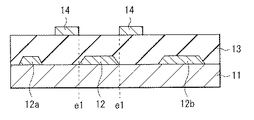
図1は、本開示の一実施の形態に係る薄膜トランジスタ(薄膜トランジスタ10)の構成を表したものである。薄膜トランジスタ(TFT:Thin Film Transistor)10は、後述の表示装置の画素回路あるいは周辺回路において用いられ、例えば酸化物TFTまたは有機TFTなどとして好適に用いられる。この薄膜トランジスタ10は、いわゆるボトムゲート・ボトムコンタクト型の素子構造を有しており、例えば基板11上の選択的な領域にゲート電極12を有している。ゲート電極12を覆うようにゲート絶縁膜13(絶縁膜)が形成されている。活性層(チャネル)を含む半導体層17aは、ゲート絶縁膜13を介して、ゲート電極12に対向配置されている。この半導体層17aに電気的に接続されて、ソース・ドレイン配線層16が形成されている。ソース・ドレイン配線層16は、基板11の側から順に積層された、第1配線層14と第2配線層15とを有する。第1配線層14は、ゲート絶縁膜13と半導体層17aとの間において、半導体層17aに下方から接している(いわゆるボトムコンタクトとして機能する)。第2配線層15は、第1配線層14の一部に重畳して設けられている。この第2配線層15上には、半導体層17aと同一材料および厚みから構成された半導体層17b(他の半導体層)が形成されている。半導体層17a,17b上には、トランジスタ全体を覆うように層間絶縁膜18が形成されている。
<Embodiment>
[Constitution]
FIG. 1 illustrates a configuration of a thin film transistor (thin film transistor 10) according to an embodiment of the present disclosure. A thin film transistor (TFT) 10 is used in a pixel circuit or a peripheral circuit of a display device to be described later, and is preferably used as an oxide TFT or an organic TFT, for example. The thin film transistor 10 has a so-called bottom gate / bottom contact type element structure, and has, for example, a
基板11は、例えばガラスから構成されている。但し、ガラス以外にも、例えばシリコン(Si)ウェハ、樹脂あるいは導電性基板などから構成されていてもよい。導電性基板としては、例えば表面を酸化シリコン(SiO2)や樹脂等により絶縁処理が施されたものが用いられる。また、基板11は、可撓性(フレキシブル性)を有する材料から構成されていてもよい。可撓性を有する材料としては、例えば、ポリイミド(PI),ポリエチレンテレフタレート(PET),ポリエーテルサルフォン(PES),ポリエチレンナフタレート(PEN),ポリカーボネート(PC),液晶ポリマーなどの樹脂材料が挙げられる。あるいは、可撓性材料としては、上記樹脂材料の他にも、薄膜化された金属シートの表面に絶縁処理が施されたものであってもよい。
The
ゲート電極12は、薄膜トランジスタ10にゲート電圧を印加し、このゲート電圧により半導体層17a中の電子密度を制御する役割を持つものである。ゲート電極12は、例えばアルミニウム(Al),チタン(Ti),白金(Pt),金(Au),パラジウム(Pd),クロム(Cr),ニッケル(Ni),モリブデン(Mo),ニオブ(Nb),ネオジム(Nd),ルビジウム(Rb),ロジウム(Rh),銀(Ag),タンタル(Ta),タングステン(W),銅(Cu)、インジウム(In)および錫(Sn)等の金属のうちのいずれかよりなる単体、またはそれらの金属のうちの少なくとも1種を含む合金から構成されている。また、これらの金属の単体および合金のうちのいずれかよりなる単層膜であってもよいし、2種以上を積層した多層膜であってもよい。一例としては、ゲート電極12は、厚み50nmのモリブデン層と、厚み400nmのアルミニウム層とを積層した多層膜である。なお、図1には、このゲート電極12と同層に形成される他の配線(配線12a,12b)についても示している。
The
ゲート絶縁膜13は、例えば無機絶縁膜により構成されている。無機絶縁膜としては、例えば酸化シリコン(SiO2),窒化シリコン(SiNx),酸窒化シリコン(SiONx),酸化アルミニウム(Al2O3)および酸化タンタル(Ta2O5)などのうちの1種よりなる単層膜、またはそれらのうちの2種以上を積層した多層膜が挙げられる。このゲート絶縁膜13の厚みは、例えば200nm〜500nmである。また、有機TFTの場合には、ゲート絶縁膜13には有機絶縁膜が用いられる。有機絶縁膜としては、例えばポリビニルフェノール(PVP),ジアリルフタレート,ポリイミド,ポリメタクリル酸メチル,ポリビニルアルコール(PVA),ポリエステル,ポリエチレン,ポリカーボネート,ポリアミド,ポリアミドイミド,ポリエーテルイミド,ポリシロキサン,ポリメタクリルアミド,ポリウレタン,ポリブタジエン,ポリスチレン,ポリ塩化ビニル,ニトリルゴム,アクリルゴム,ブチルゴム,エポキシ樹脂,フェノール樹脂,メラミン樹脂,ウレア樹脂,ノボラック樹脂,フッ素系樹脂などのうちの1種よりなる単層膜、またはそれらのうちの2種以上よりなる多層膜が挙げられる。
The
ソース・ドレイン配線層16は、ソースまたはドレインとして機能するものである。ここでは、ゲート絶縁膜13上の2箇所に、互いに電気的に分離された状態で、一方がソースとして、他方がドレインとしてそれぞれ機能するように設けられている。
The source /
第1配線層14は、ゲート絶縁膜13と半導体層17aとの間に、少なくとも一部が挟まれるように形成され、半導体層17aに対して下方から接している(ボトムコンタクトを形成する)。換言すると、第1配線層14の一部は、ゲート絶縁膜13上において、半導体層17aにより覆われている。第1配線層14のうち半導体層17aから露出した部分は、第2配線層15により覆われている(第1配線層14は、半導体層17aと第2配線層15とによって覆われている)。この第1配線層14は、後述のセルフアラインプロセスを用いて形成されるものである。具体的には、第1配線層14をパターニングする際のフォトリソグラフィの露光プロセスにおいて、ゲート電極12をマスクとした裏面露光により、フォトレジストのパターニングがなされる。このようなプロセスが用いられることにより、第1配線層14の端部は、平面視的にゲート電極12の端部と非重畳となる。また、2つの第1配線層14間の距離(距離B)は、ゲート電極12の幅と略等しくなる。換言すると、第1配線層14の端部は、ゲート電極12の端部と平面視的に略同一の位置(図1に示した位置e1)に配される。距離Bは、チャネル長に相当する。
The
この第1配線層14は、例えば酸化インジウム錫(ITO),酸化インジウム亜鉛(IZO),酸化インジウムガリウム亜鉛(IGZO),酸化インジウムスズ亜鉛(ITZO),酸化亜鉛(ZnO),酸化インジウムガリウム(IGO)あるいは酸化インジウム(InO)等の透明導電膜から構成されている。第1配線層14の厚みは、例えば10nm〜50nmである。
The
第2配線層15は、第1配線層14よりも導電性の高い導電膜、例えば金属により構成されていることが望ましい。第2配線層15を構成する金属としては、例えばアルミニウム(Al)もしくは銀(Ag)の単体、またはアルミニウムもしくは銀を主成分とする合金などが挙げられる。但し、第2配線層15の構成材料は、金属に限定されず、第1配線層14として用いられるような透明導電膜により構成されていてもよい。ソース・ドレイン配線層16を、第1配線層14の単層膜とする場合に比べ、低抵抗化できるためである。但し、より抵抗値を低減するために、第2配線層15は金属により構成されることが望ましい。この第2配線層15の厚みは、半導体層17aよりも大きく、例えば1μm〜2μmである。第2配線層15の厚みは、第2配線層15の端部(側面)において半導体層17aが断切れする(端部において分断される)のに十分な大きさを有していることが望ましい。この第2配線層15は、ゲート絶縁膜13上において、2つの第1配線層14の各一部に重畳して、設けられている。第2配線層15は、半導体層17aに非重畳となっている。
The
半導体層17aは、ゲート電圧の印加によってソースおよびドレイン間の領域にチャネルを形成するものである。この半導体層17aは、例えば酸化物半導体により構成されている。酸化物半導体は、例えばインジウム(In),ガリウム(Ga),亜鉛(Zn),スズ(Sn)等のうちの少なくとも1種の元素と、酸素とを含む化合物である。具体的には、例えば酸化インジウムガリウム亜鉛(IGZO),酸化インジウムスズ亜鉛(ITZO),酸化亜鉛(ZnO),酸化インジウム亜鉛(IZO),酸化インジウムガリウム(IGO),酸化インジウムスズ(ITO),酸化インジウム(InO)等が挙げられる。また、有機TFTの場合には、半導体層17aには有機半導体が用いられる。有機半導体は、例えばポリチオフェン、ポリピロール、ポリアニリン、ポリアセチレン、ポリフェニレン、ポリフラン、ポリセレノフェン、ポリイソチアナフテン、ポリフェニレンスルフィド、ポリフェニレンビニレン、ポリチエニレンビニレン、ポリナフタレン、ポリアントラセン、ポリピレン、ポリアズレン、フタロシアニン、ペンタセン、メロシアニン、およびポリエチレンジオキシチオフェンから成る群から選択された少なくとも1種類の有機材料に、ヨウ素、過塩素酸、塩酸、硫酸、硝酸、リン酸、4フッ化硼酸、5フッ化ヒ素、6フッ化リン酸、アルキルスルホン酸、パーフルオアルキルスルホン酸、ポリアクリル酸、ポリスチレンスルホン酸、およびドデシルベンゼンスルホン酸から成る群から選択された少なくとも1種類のドーピング材料をドーピングして得られた材料である。この半導体層17aの厚みは、例えば10nm〜50nm程度である。
The
この半導体層17aは、詳細は後述するが、ソース・ドレイン配線層16の第2配線層15の形成後に成膜されることで、第2配線層15の端部での断切れによって、一部分がパターン形成される。半導体層17aは、第1配線層14の一部(端部および上面の一部)を覆うと共に、第2配線層15によって挟まれた領域に形成されている。また、第2配線層15上の一部にも、半導体層17aと同一の材料および厚みからなる半導体層17bが形成される。この半導体層17bは、半導体層17aの形成時において、半導体層17aと分断されて第2配線層15上に堆積した半導体材料である。
As will be described in detail later, the
層間絶縁膜18は、例えば酸化シリコン、窒化シリコンおよび酸化アルミニウム等の無機絶縁膜、あるいはアクリル、ポリイミドおよびシロキサン等の有機絶縁膜から構成されている。
The
[製造方法]
次に、薄膜トランジスタ10の製造方法について説明する。図2A〜図7は、薄膜トランジスタ10の製造方法を工程順に説明するための断面図である。
[Production method]
Next, a method for manufacturing the thin film transistor 10 will be described. 2A to 7 are cross-sectional views for explaining the manufacturing method of the thin film transistor 10 in the order of steps.
まず、基板11上に、ゲート電極12(および配線層12a,12b)と、ゲート絶縁膜13とをこの順に形成する。
First, the gate electrode 12 (and the wiring layers 12a and 12b) and the
(第1配線層の形成)
第1配線層14は、セルフアラインプロセスを用いてパターン形成する。具体的には、まず、図2Aに示したように、ゲート絶縁膜13上の全面にわたって、上述した材料および厚みよりなる第1配線層14を、例えばスパッタ法により成膜する。
(Formation of the first wiring layer)
The
続いて、図2Bに示したように、第1配線層14上の選択的な領域に、フォトレジスト膜110Aを形成する。このフォトレジスト膜110Aは、ソース・ドレイン配線層16の形成領域(薄膜トランジスタ10の形成領域)に対応する領域に形成される。
Subsequently, as illustrated in FIG. 2B, a photoresist film 110 </ b> A is formed in a selective region on the
この後、図2Cに示したように、フォトレジスト膜110Aをマスクとしたエッチングを行い、第1配線層14をパターニングする。エッチング後、フォトレジスト膜110Aは第1配線層14上から剥離する。
Thereafter, as shown in FIG. 2C, etching is performed using the photoresist film 110A as a mask, and the
次に、図3Aに示したように、第1配線層14上にフォトレジスト膜110Bを形成し、裏面露光を行う。即ち、ゲート電極12をマスクとしてセルフアラインにより露光する。具体的には、基板11の下方から光Lを照射することで、フォトレジスト膜110Bを露光する。このとき、フォトレジスト膜110Bとして、いわゆるネガ型の感光性樹脂を用いることで、図3Bに示したように、ゲート電極12(および配線層12a,12b)がマスクとなり、このゲート電極12等から露出した領域にのみ、フォトレジスト膜110Bが残る。
Next, as shown in FIG. 3A, a
この後、図3Cに示したように、フォトレジスト膜110Bをマスクとして、第1配線層14のエッチングを行う。この後、図3Dに示したように、フォトレジスト膜110Bを剥離することにより、所望の領域に第1配線層14がパターン形成される。これにより、第1配線層14とゲート電極12とが平面視的に非重畳となるように形成され、第1配線層14の端部と、ゲート電極12の端部とは、略同一の位置に配される。このようにして、セルフアラインプロセスを利用して、第1配線層14を形成することができる。
Thereafter, as shown in FIG. 3C, the
(第2配線層の形成)
次に、第2配線層15を形成する。即ち、まず、ゲート絶縁膜13に、層間接続のためのコンタクトホールH1を形成する。具体的には、図4Aに示したように、ゲート絶縁膜13および第1配線層14の上に、フォトレジスト膜110Cをパターン形成し、このフォトレジスト膜110Cをマスクとしてゲート絶縁膜13をエッチングする。これにより、ゲート絶縁膜13の、所望の領域(例えば、配線層12aに対応する領域)に、コンタクトホールH1を形成できる。この後、フォトレジスト膜110Cは、ゲート絶縁膜13上から剥離する。
(Formation of second wiring layer)
Next, the
続いて、図4Bに示したように、ゲート絶縁膜13上に、第1配線層14を覆い、かつコンタクトホールH1を埋め込んで、上述した材料および厚みよりなる第2配線層15を、例えば真空蒸着法あるいはスパッタ法等により成膜する。
Subsequently, as shown in FIG. 4B, the
この後、図4Cに示したように、フォトレジスト膜110Dをパターン形成し、このフォトレジスト膜110Dをマスクとして第2配線層15をエッチングする。なお、フォトレジスト膜110Dは、第1配線層14の一部に重畳するようにパターニングする。このフォトレジスト膜110Dを用いたエッチングにより、第1配線層14の一部に重畳するように第2配線層15がパターン形成される。
Thereafter, as shown in FIG. 4C, a
その後、図4Dに示したように、フォトレジスト膜110Dを第2配線層15上から剥離する。このようにして、第2配線層15が形成され、即ちソース・ドレイン配線層16が形成される。なお、第1配線層14のうち第2配線層15から露出した部分が、後の工程において形成する半導体層17aとのコンタクト部分となる。
Thereafter, as shown in FIG. 4D, the photoresist film 110 </ b> D is peeled off from the
(半導体層の形成)
次に、半導体層17aを形成する。具体的には、図5Aに示したように、上述した材料(例えば酸化物半導体)および厚みよりなる半導体層17aを、例えばスパッタ法などにより成膜する。このとき、第2配線層15の端部(側面)において、上述した半導体材料が断切れして(分断されて)堆積する。即ち、第2配線層15間に挟まれた領域に半導体層17aが、第1配線層14と接して形成される。第2配線層15上には、半導体層17aと分かれて半導体層17bが形成される。このように、本実施の形態では、第2配線層15によって、半導体層17aの一部分(例えば半導体層17aのゲート長方向における形状)がパターニングされる。また、確実に断切れさせるために、第2配線層15の厚みは半導体層17aの厚みに比べて十分に大きいことが望ましい。
(Formation of semiconductor layer)
Next, the
この後、図5Bおよび図6に示したように、半導体層17aのうちゲート絶縁膜13上に配された一部を、例えばフォトリソグイラフィ法を用いたエッチングによりパターニングする。なお、図6は、図5Bの要部構成の平面レイアウトを表したものである。ここで、第1配線層14は、酸化物半導体などの透明導電膜により構成されることから、半導体層17aとエッチング選択比を確保しにくく(条件設定が難しく)、エッチングが困難である。本実施の形態では、第1配線層14は、第2配線層15と半導体層17aとによって被覆されている。半導体層17aのエッチングは、ゲート絶縁膜13上と、半導体層17aに比べて十分に厚みの大きな第2配線層15上とにおいてなされることとなる。したがって、上記のような難しい選択性エッチングの工程を経ることなく、容易に、半導体層17aを第1配線層14上の所望の領域に形成することができる。このようにして、半導体層17aを形成することができる。また、図6に示したように、平面視的には、第1配線層14は、位置e1においてゲート電極12と隣接すると共に、第2配線層15および半導体層17aによって全体が覆われている。また、第2配線層15は、第1配線層14の一部に重畳すると共に、半導体層17aとは非重畳となっている。第2配線層15の上には、半導体層17bが形成される。上記のようにして、薄膜トランジスタ10が完成する。
Thereafter, as shown in FIGS. 5B and 6, a part of the
最後に、図7に示したように、層間絶縁膜18を形成し、酸素(O2)雰囲気においてアニール処理を行う。この際、第1配線層14は、上述のように半導体層14と第2配線層15とによって覆われていることから、酸素雰囲気に曝されない。このため、半導体層17aとのコンタクト部分となる第1配線層14の高抵抗化を抑制することができる。また、このアニール処理は、層間絶縁膜18の形成以前の工程において行ってもよいが、薄膜トランジスタ10の完成後にアニール処理を行うことが望ましい。TFT特性をより安定化させることができるためである。
Finally, as shown in FIG. 7, an
[作用・効果]
本実施の形態の薄膜トランジスタ10では、ゲート電極12に印加されるゲート電圧に応じて、ソース・ドレイン配線層16間(ソースおよびドレイン間)の電流が制御され、オン動作またはオフ動作がなされる。例えば、ゲート電極12に、所定の閾値電圧以上のゲート電圧が印加されると、半導体層17aのチャネルに電界が生じ、ソース・ドレイン配線層16間に電流が流れ、オン状態となる。後述の表示装置の各種回路において、例えばスイッチング素子あるいは増幅素子などとして用いることができる。
[Action / Effect]
In the thin film transistor 10 of the present embodiment, the current between the source / drain wiring layers 16 (between the source and the drain) is controlled according to the gate voltage applied to the
ここで、薄膜トランジスタ10では、ボトムコンタクト型の構造をもつことにより、トップコンタクト型の構造に比べ、ゲート電極12をマスクとした裏面露光(セルフアラインプロセス)を利用することができる。これにより、以下のようなメリットがある。
Here, since the thin film transistor 10 has a bottom contact type structure, backside exposure (self-alignment process) using the
図8に、本実施の形態の比較例(比較例1)として、トップコンタクト型のTFTの構成例について示す。図9は、図8の要部の平面レイアウトを表したものである。この比較例1のTFTでは、ゲート電極102上に、ゲート絶縁膜103を介して半導体層107が形成されている。この半導体層107の上面に接するようにソース・ドレイン配線層(コンタクト層108a,配線層108b)が形成されている。これらの素子全体を覆うように、層間絶縁膜109が形成されている。
FIG. 8 shows a configuration example of a top contact TFT as a comparative example (Comparative Example 1) of this embodiment. FIG. 9 shows a planar layout of the main part of FIG. In the TFT of Comparative Example 1, a
比較例1の構造では、コンタクト層108aとゲート電極102とが、オーバーラップするように配置されている(オーバーラップ領域dOL1が設けられる)。これは、例えば酸化物TFTでは、半導体層107に対する有効な不純物ドーパントが乏しいことから、いわゆるLDD(Lightly Doped Drain)工程が行われないためである。ところが、このオーバーラップ領域dOL1の形成により、寄生容量が大きくなり易い。また、トップコンタクト型の素子構造では、コンタクト層108aの形成時(コンタクトホールの形成時)に半導体層107上でエッチングを行うことから、チャネルへのエッチングダメージが生じ易い。加えて、リソばらつきを考慮して、配線層108bと半導体層107との間には、オーバーラップ領域dOL2が設けられている。このオーバーラップ領域dOL2に起因して、半導体層107のチャネルに電気的ストレスがかかり易い。更には、チャネル長Lgは、配線層108b同士のショートマージンと、コンタクト層108aおよび配線層108b間の位置合わせマージンとの制約を受ける。このため、チャネル長Lgの微細化が難しい。
In the structure of Comparative Example 1, the
これに対し、本実施の形態のように、ボトムコンタクト型の素子構造において、上述のようなセルフアラインによる裏面露光プロセスを用いることで、上記のオーバーラップ領域dOL1を最小化できる。即ち、図1および図6に示したように、コンタクト層となる第1配線層14は、ゲート電極12と非重畳となり、詳細には第1配線層14の端部とゲート電極12の端部とが略同一の位置e1に配される。このため、寄生容量を低減することができる。また、ゲート電極12と第1配線層14との間において位置ずれ,ばらつきが生じにくい。このため、保持容量の面積縮小につながると共に、寄生容量による保持容量のばらつきに起因した色むらの抑制につながる。
On the other hand, the
また、第1配線層14による半導体層17aへのボトムコンタクトにより、第1配線層14を半導体層17aよりも先に形成することから、比較例1のようなコンタクト形成のための半導体層107上でのエッチング工程が不要である。このため、半導体層17aへのエッチングダメージが生じず、信頼性低下およびTFT特性のばらつきを低減することができる。
Further, since the
加えて、第2配線層15は半導体層17aに非重畳であることから、半導体層17aへの電気的ストレスを軽減できる。このため、BTI(Bias Temperature Instability)信頼性低下を抑制でき、また寄生容量を最小化することができる。
In addition, since the
更には、チャネル長が第1配線層14間の距離Bによって決まることから、チャネル長の微細化が可能である。 Furthermore, since the channel length is determined by the distance B between the first wiring layers 14, the channel length can be miniaturized.
図10A〜図10Eに、本実施の形態の比較例2として、ボトムコンタクト型のTFTの製造工程の一例について示す。例えば、図10Aおよび図10Bに示したように、基板101上に、ゲート電極102、ゲート絶縁膜103、透明導電膜よりなるコンタクト層104およびフォトレジスト膜105を形成した後、裏面露光により、フォトレジスト膜105をパターニングする。続いて、図10Cに示したように、フォトレジスト膜105をマスクとしてエッチングを行ったのち、図10Dに示したように、フォトレジスト膜105を除去する。この後、図10Eに示したように、コンタクト層104上に、例えば酸化物半導体よりなる半導体層106を成膜し、パターニングする。ところが、この比較例2の手法では、半導体層106のパターニングにおいて、コンタクト層104上においてエッチングが行われる。コンタクト層104(透明導電膜)と、半導体層106(酸化物半導体)との間で選択性をもって(選択比を確保する)ことは容易ではなく、エッチングが非常に困難である。また、コンタクト層104は、金属に比べて抵抗値が高く、配線利用には不向きである。例えば有機電界発光装置向けの駆動ドライバなどでは、大電流を要し、現実的ではない。加えて、TFTの特性安定化の目的で、チャネル形成後にアニール処理が行われるが、このアニール処理によって抵抗値が高くなり易い。特に、酸化物TFTでは、酸素雰囲気においてアニール処理がなされることから、透明導電膜の抵抗値上昇が顕著である。
10A to 10E show an example of a manufacturing process of a bottom contact type TFT as Comparative Example 2 of the present embodiment. For example, as shown in FIGS. 10A and 10B, a
これに対し、本実施の形態では、ソース・ドレイン配線層16において、第1配線層14(ボトムコンタクト)の一部に重畳して第2配線層15が設けられている。これにより、第1配線層14のみの単層構造とする場合に比べ、ソース・ドレイン配線層16を低抵抗化できる。また、製造プロセスでは、第2配線層15の形成後に半導体層17aが形成され、第2配線層15の端部において半導体材料が分断される(半導体層17a,17bが形成される)。このため、第1配線層14上において半導体層17aをエッチングする必要がない。第1配線層14と半導体層17aとの選択性をもった難しいエッチングを行うことなく、半導体層17aを所望の領域にパターン形成することができる。
In contrast, in the present embodiment, in the source /
また、チャネル形成後のアニール処理の際に、第1配線層14の露出がない(半導体層17aおよび第2配線層15によって覆われている)ことから、第1配線層14の高抵抗化を抑制することができる。加えて、このアニール処理を製造工程の最後(層間絶縁膜18の形成後など)に行うことができ、TFT特性の安定化に有利となる。
In addition, since the
更に、上述したようなソース・ドレイン配線層16の低抵抗化、寄生容量の低減、TFT特性の安定化、信頼性の向上などの効果によって、薄膜トランジスタ10の高速動作が可能となる。このような薄膜トランジスタ10を表示装置に適用した場合には、ハイフレームレートでの映像表示を実現できる。
Further, the thin film transistor 10 can be operated at high speed due to the effects such as the reduction in resistance of the source /
以上のように、本実施の形態では、ソース・ドレイン配線層16が、透明導電膜からなる第1配線層14と、第1配線層14の一部に重畳する第2配線層15とを有する。第2配線層15が第1配線層14に重畳することで、ソース・ドレイン配線層16を低抵抗化できる。また、製造プロセスでは、第2配線層15の形成後に半導体層17aが形成されることで、第2配線層15の端部において半導体材料が分断されることから、第1配線層14と半導体層17aとの間で選択性をもつエッチングを行うことなく、半導体層17aを所望の領域にパターン形成することができる。よって、製造プロセスの容易化と低電圧駆動とを実現することが可能となる。
As described above, in the present embodiment, the source /
(表示装置の例)
上記のような薄膜トランジスタ10は、例えば次のような表示装置(液晶表示装置1,有機電界発光装置2)に適用することができる。図11は、液晶表示装置1の概略構成を、図12は、有機電界発光装置2の概略構成を、それぞれ表したものである。
(Example of display device)
The thin film transistor 10 as described above can be applied to, for example, the following display devices (the liquid
図11に示したように、液晶表示装置1では、基板11上に、上述した薄膜トランジスタ10が形成され、この薄膜トランジスタ10上に層間絶縁膜18を介して画素電極19が設けられる。画素電極19は、例えば画素(サブピクセル)毎に設けられている。この画素電極19と対向して各画素に共通の対向電極21が設けられ、これらの画素電極19と対向電極21との間に、液晶層20が封止されている。なお、図示は省略するが、対向電極21上には、対向基板が設けられている。対向基板には、カラーフィルタやブラックマトリクスなどが形成されている。また、基板11の光入射側と、対向基板の光出射側とには、偏光板が貼り合わせられている。
As shown in FIG. 11, in the liquid
図12に示したように、有機電界装置2では、基板11上に、上述した薄膜トランジスタ10が形成され、この薄膜トランジスタ10上に層間絶縁膜18を介して第1電極22が設けられる。第1電極22は、例えば画素(サブピクセル)毎に設けられている。この第1電極22と対向して、各画素に共通の第2電極24が設けられ、これらの第1電極22と第2電極24との間に、有機電界発光層を含む有機層23が形成されている。なお、第1電極22、有機層23および第2電極24が、後述の有機電界発光素子2Aに相当する。また、図示は省略するが、第2電極24上に保護膜や接着層を介して封止基板が貼り合わせられている。封止基板には、必要に応じて、カラーフィルタやブラックマトリクスなどが形成されている。
As shown in FIG. 12, in the organic
図13は、上記の有機電界発光装置2の機能構成を表したものである。このように、有機電界発光装置2では、基板11上の表示領域11Aには、それぞれが有機電界発光素子2Aを含む複数の画素140がマトリクス状に配置されている。各画素140は、例えば赤色の光(波長620nm〜750nm),緑色の光(波長495nm〜570nm)および青色の光(波長450nm〜495nm)のうちのいずれかを出射する。画素140はサブピクセル(R画素,G画素,B画素)に相当するものであり、これら3つのR画素,G画素,B画素の組を1つのピクセルとして画像表示がなされる。表示領域11Aの周辺には、映像表示用の信号線駆動回路120および走査線駆動回路130が設けられている。
FIG. 13 shows a functional configuration of the
画素140は、図14に示したように駆動用のトランジスタTr1および書き込み用のトランジスタTr2を有し、これらのトランジスタTr1,Tr2の間にはキャパシタCsが設けられている。第1の電源ライン(Vcc)と第2の電源ライン(GND)との間において、有機電界発光素子2AがトランジスタTr1に直列に接続されている。信号線駆動回路120は、列方向に配置された複数の信号線120Aを通じてトランジスタTr2のソース電極に画像信号を供給する。走査線駆動回路130は、行方向に配置された複数の走査線130Aを通じてトランジスタTr2のゲート電極に走査信号を順次供給する。これらのトランジスタTr1,Tr2として、上述した薄膜トランジスタ10を用いることができる。
As shown in FIG. 14, the
<適用例>
上記実施の形態において説明した薄膜トランジスタ10を含む表示装置は、外部から入力された映像信号あるいは内部で生成した映像信号を、映像として表示するあらゆる分野の電子機器に用いることができる。以下にその具体例を示す。但し、この他にも、上述の表示装置は、例えばテレビジョン装置,デジタルカメラ,ビデオカメラ,ノート型パーソナルコンピュータ、フレキシブルディスプレイ等の電子機器に組み込むことができる。
<Application example>
The display device including the thin film transistor 10 described in the above embodiment can be used for electronic devices in various fields that display a video signal input from the outside or a video signal generated inside as a video. Specific examples are shown below. However, the display device described above can be incorporated into electronic devices such as a television device, a digital camera, a video camera, a notebook personal computer, and a flexible display.
図15Aおよび図15Bは、スマートフォン220の外観を表したものである。このスマートフォン220は、例えば、表側に表示部221および操作部222を有し、裏側にカメラ223を有しており、表示部221に上記実施の形態の表示装置が搭載されている。
FIG. 15A and FIG. 15B represent the appearance of the
図16は、タブレットパーソナルコンピュータ240の外観を表したものである。このタブレットパーソナルコンピュータ240は、例えば、タッチパネル部241および筐体242を有しており、タッチパネル部241に上記実施の形態の表示装置が搭載されている。 FIG. 16 shows the appearance of the tablet personal computer 240. The tablet personal computer 240 includes, for example, a touch panel unit 241 and a housing 242, and the display device of the above embodiment is mounted on the touch panel unit 241.
図17Aおよび図17Bは、携帯電話機290の外観を表したものである。この携帯電話機290は、例えば、上側筐体291と下側筐体292とを連結部(ヒンジ部)293で連結したものであり、ディスプレイ294,サブディスプレイ295,ピクチャーライト296およびカメラ297を有している。ディスプレイ294またはサブディスプレイ295が上記実施の形態の表示装置により構成されている。
FIG. 17A and FIG. 17B show the appearance of the
図18は、透明ディスプレイ300の外観を表したものである。透明ディスプレイ300は、例えば表示部310と、操作部311と、筐体312とを有している。表示部310が上記実施の形態の表示装置により構成されている。この透明ディスプレイ300では、表示部310の背景を透過しつつ、画像や文字情報を表示することが可能である。
FIG. 18 shows the appearance of the transparent display 300. The transparent display 300 includes, for example, a display unit 310, an
以上、実施の形態を挙げて説明したが、本開示は上記実施の形態に限定されるものではなく、種々変形が可能である。例えば、上記実施の形態に記載した各層の材料および厚みは列挙したものに限定されるものではなく、他の材料および厚みとしてもよい。また、表示装置では、上述した全ての層を備えている必要はなく、あるいは上述した各層に加えて更に他の層を備えていてもよい。また、上記実施の形態等において説明した効果は一例であり、本開示の効果は、他の効果であってもよいし、更に他の効果を含んでいてもよい。 As described above, the embodiments have been described. However, the present disclosure is not limited to the above-described embodiments, and various modifications can be made. For example, the material and thickness of each layer described in the above embodiment are not limited to those listed, and other materials and thicknesses may be used. In addition, the display device does not have to include all the layers described above, or may include other layers in addition to the layers described above. Moreover, the effect demonstrated in the said embodiment etc. is an example, The effect of this indication may be other effects and may also contain other effects.
なお、本開示は以下のような構成であってもよい。
(1)
ゲート電極と、
前記ゲート電極上に配置された絶縁膜と、
前記絶縁膜を介して前記ゲート電極に対向配置された半導体層と、
前記半導体層と電気的に接続されたソース・ドレイン配線層と
を備え、
前記ソース・ドレイン配線層は、
前記半導体層と前記絶縁膜との間において前記半導体層に接すると共に、透明導電膜からなる第1の配線層と、
前記第1の配線層の一部に重畳して設けられた第2の配線層と
を有し、
前記半導体層と同一材料からなる他の半導体層が、前記第2の配線層上に積層されている
薄膜トランジスタ。
(2)
前記第1の配線層は、平面視的に前記ゲート電極の端部に非重畳である
上記(1)に記載の薄膜トランジスタ。
(3)
前記第1の配線層の端部は、平面視的に前記ゲート電極の端部と略同一の位置に配置されている
上記(2)に記載の薄膜トランジスタ。
(4)
前記第2の配線層は、金属から構成されている
上記(1)〜(3)のいずれかに記載の薄膜トランジスタ。
(5)
前記第2の配線層は、前記半導体層よりも厚みが大きい
上記(1)〜(4)のいずれかに記載の薄膜トランジスタ。
(6)
前記第2の配線層は、前記半導体層と非重畳である
上記(1)〜(5)のいずれかに記載の薄膜トランジスタ。
(7)
前記第1の配線層は、前記半導体層と前記第2の配線層とにより覆われている
上記(1)〜(6)のいずれかに記載の薄膜トランジスタ。
(8)
前記半導体層は、酸化物半導体から構成されている
上記(1)〜(7)のいずれかに記載の薄膜トランジスタ。
(9)
前記半導体層は、有機半導体から構成されている
上記(1)〜(8)のいずれかに記載の薄膜トランジスタ。
(10)
ゲート電極を形成する工程と、
前記ゲート電極上に絶縁膜を形成する工程と、
前記絶縁膜を介して前記ゲート電極に対向配置された半導体層を形成する工程と、
前記半導体層と電気的に接続されたソース・ドレイン配線層を形成する工程と
を含み、
前記ソース・ドレイン配線層として、透明導電膜からなる第1の配線層と、前記第1の配線層の一部に重畳する第2の配線層とをこの順に形成し、
前記第2の配線層を形成した後、前記半導体層を形成する
薄膜トランジスタの製造方法。
(11)
前記第1の配線層を、前記ゲート電極をマスクとした露光プロセスを含むフォトリソグラフィにより形成する
上記(10)に記載の薄膜トランジスタの製造方法。
(12)
前記第2の配線層は、金属から構成されている
上記(10)または(11)に記載の薄膜トランジスタの製造方法。
(13)
前記第2の配線層の厚みを、前記半導体層の厚みよりも大きくする
上記(10)〜(12)のいずれかに記載の薄膜トランジスタの製造方法。
(14)
前記第1の配線層は、前記半導体層と前記第2の配線層とにより覆われている
上記(10)〜(13)のいずれかに記載の薄膜トランジスタの製造方法。
(15)
前記半導体層は、酸化物半導体から構成されている
上記(10)〜(14)のいずれかに記載の薄膜トランジスタの製造方法。
(16)
前記半導体層は、有機半導体から構成されている
上記(10)〜(14)のいずれかに記載の薄膜トランジスタの製造方法。
(17)
ゲート電極と、
前記ゲート電極上に配置された絶縁膜と、
前記絶縁膜を介して前記ゲート電極に対向配置された半導体層と、
前記半導体層と電気的に接続されたソース・ドレイン配線層と
を備え、
前記ソース・ドレイン配線層は、
前記半導体層と前記絶縁膜との間において前記半導体層に接すると共に、透明導電膜からなる第1の配線層と、
前記第1の配線層の一部に重畳して設けられた第2の配線層と
を有し、
前記半導体層と同一材料からなる他の半導体層が、前記第2の配線層上に積層されている
薄膜トランジスタを備えた表示装置。
The present disclosure may be configured as follows.
(1)
A gate electrode;
An insulating film disposed on the gate electrode;
A semiconductor layer disposed opposite to the gate electrode through the insulating film;
A source / drain wiring layer electrically connected to the semiconductor layer,
The source / drain wiring layer is
A first wiring layer made of a transparent conductive film and in contact with the semiconductor layer between the semiconductor layer and the insulating film;
A second wiring layer provided so as to overlap with a part of the first wiring layer,
A thin film transistor in which another semiconductor layer made of the same material as that of the semiconductor layer is stacked on the second wiring layer.
(2)
The thin film transistor according to (1), wherein the first wiring layer is not overlapped with an end portion of the gate electrode in a plan view.
(3)
The thin film transistor according to (2), wherein an end portion of the first wiring layer is disposed at substantially the same position as the end portion of the gate electrode in plan view.
(4)
The thin film transistor according to any one of (1) to (3), wherein the second wiring layer is made of metal.
(5)
The thin film transistor according to any one of (1) to (4), wherein the second wiring layer is thicker than the semiconductor layer.
(6)
The thin film transistor according to any one of (1) to (5), wherein the second wiring layer is non-overlapping with the semiconductor layer.
(7)
The thin film transistor according to any one of (1) to (6), wherein the first wiring layer is covered with the semiconductor layer and the second wiring layer.
(8)
The thin film transistor according to any one of (1) to (7), wherein the semiconductor layer is made of an oxide semiconductor.
(9)
The said semiconductor layer is comprised from the organic semiconductor. The thin-film transistor in any one of said (1)-(8).
(10)
Forming a gate electrode;
Forming an insulating film on the gate electrode;
Forming a semiconductor layer disposed opposite to the gate electrode through the insulating film;
Forming a source / drain wiring layer electrically connected to the semiconductor layer,
As the source / drain wiring layer, a first wiring layer made of a transparent conductive film and a second wiring layer overlapping with a part of the first wiring layer are formed in this order,
A method of manufacturing a thin film transistor, wherein the semiconductor layer is formed after forming the second wiring layer.
(11)
The method for manufacturing a thin film transistor according to (10), wherein the first wiring layer is formed by photolithography including an exposure process using the gate electrode as a mask.
(12)
The method for manufacturing a thin film transistor according to (10) or (11), wherein the second wiring layer is made of metal.
(13)
The method for manufacturing a thin film transistor according to any one of (10) to (12), wherein the thickness of the second wiring layer is larger than the thickness of the semiconductor layer.
(14)
The method of manufacturing a thin film transistor according to any one of (10) to (13), wherein the first wiring layer is covered with the semiconductor layer and the second wiring layer.
(15)
The said semiconductor layer is comprised from the oxide semiconductor. The manufacturing method of the thin-film transistor in any one of said (10)-(14).
(16)
The said semiconductor layer is comprised from the organic semiconductor. The manufacturing method of the thin-film transistor in any one of said (10)-(14).
(17)
A gate electrode;
An insulating film disposed on the gate electrode;
A semiconductor layer disposed opposite to the gate electrode through the insulating film;
A source / drain wiring layer electrically connected to the semiconductor layer,
The source / drain wiring layer is
A first wiring layer made of a transparent conductive film and in contact with the semiconductor layer between the semiconductor layer and the insulating film;
A second wiring layer provided so as to overlap with a part of the first wiring layer,
A display device comprising: a thin film transistor in which another semiconductor layer made of the same material as the semiconductor layer is stacked on the second wiring layer.
10…薄膜トランジスタ、11…基板、12…ゲート電極、13…ゲート絶縁膜、14…第1配線層、15…第2配線層、16…ソース・ドレイン配線層、17a,17b…半導体層、18…層間絶縁膜、1…液晶表示装置、2…有機電界発光装置、2A…有機電界発光素子、110A〜110D…フォトレジスト膜。 DESCRIPTION OF SYMBOLS 10 ... Thin-film transistor, 11 ... Board | substrate, 12 ... Gate electrode, 13 ... Gate insulating film, 14 ... 1st wiring layer, 15 ... 2nd wiring layer, 16 ... Source-drain wiring layer, 17a, 17b ... Semiconductor layer, 18 ... Interlayer insulating film, 1 ... liquid crystal display device, 2 ... organic electroluminescent device, 2A ... organic electroluminescent element, 110A-110D ... photoresist film.
Claims (17)
前記ゲート電極上に配置された絶縁膜と、
前記絶縁膜を介して前記ゲート電極に対向配置された半導体層と、
前記半導体層と電気的に接続されたソース・ドレイン配線層と
を備え、
前記ソース・ドレイン配線層は、
前記半導体層と前記絶縁膜との間において前記半導体層に接すると共に、透明導電膜からなる第1の配線層と、
前記第1の配線層の一部に重畳して設けられた第2の配線層と
を有し、
前記半導体層と同一材料からなる他の半導体層が、前記第2の配線層上に積層されている
薄膜トランジスタ。 A gate electrode;
An insulating film disposed on the gate electrode;
A semiconductor layer disposed opposite to the gate electrode through the insulating film;
A source / drain wiring layer electrically connected to the semiconductor layer,
The source / drain wiring layer is
A first wiring layer made of a transparent conductive film and in contact with the semiconductor layer between the semiconductor layer and the insulating film;
A second wiring layer provided so as to overlap with a part of the first wiring layer,
A thin film transistor in which another semiconductor layer made of the same material as that of the semiconductor layer is stacked on the second wiring layer.
請求項1に記載の薄膜トランジスタ。 The thin film transistor according to claim 1, wherein the first wiring layer is not superimposed on an end portion of the gate electrode in plan view.
請求項2に記載の薄膜トランジスタ。 The thin film transistor according to claim 2, wherein an end portion of the first wiring layer is disposed at substantially the same position as the end portion of the gate electrode in plan view.
請求項1に記載の薄膜トランジスタ。 The thin film transistor according to claim 1, wherein the second wiring layer is made of metal.
請求項1に記載の薄膜トランジスタ。 The thin film transistor according to claim 1, wherein the second wiring layer is thicker than the semiconductor layer.
請求項1に記載の薄膜トランジスタ。 The thin film transistor according to claim 1, wherein the second wiring layer is non-overlapping with the semiconductor layer.
請求項1に記載の薄膜トランジスタ。 The thin film transistor according to claim 1, wherein the first wiring layer is covered with the semiconductor layer and the second wiring layer.
請求項1に記載の薄膜トランジスタ。 The thin film transistor according to claim 1, wherein the semiconductor layer is made of an oxide semiconductor.
請求項1に記載の薄膜トランジスタ。 The thin film transistor according to claim 1, wherein the semiconductor layer is made of an organic semiconductor.
前記ゲート電極上に絶縁膜を形成する工程と、
前記絶縁膜を介して前記ゲート電極に対向配置された半導体層を形成する工程と、
前記半導体層と電気的に接続されたソース・ドレイン配線層を形成する工程と
を含み、
前記ソース・ドレイン配線層として、透明導電膜からなる第1の配線層と、前記第1の配線層の一部に重畳する第2の配線層とをこの順に形成し、
前記第2の配線層を形成した後、前記半導体層を形成する
薄膜トランジスタの製造方法。 Forming a gate electrode;
Forming an insulating film on the gate electrode;
Forming a semiconductor layer disposed opposite to the gate electrode through the insulating film;
Forming a source / drain wiring layer electrically connected to the semiconductor layer,
As the source / drain wiring layer, a first wiring layer made of a transparent conductive film and a second wiring layer overlapping with a part of the first wiring layer are formed in this order,
A method of manufacturing a thin film transistor, wherein the semiconductor layer is formed after forming the second wiring layer.
請求項10に記載の薄膜トランジスタの製造方法。 The method of manufacturing a thin film transistor according to claim 10, wherein the first wiring layer is formed by photolithography including an exposure process using the gate electrode as a mask.
請求項10に記載の薄膜トランジスタの製造方法。 The method for manufacturing a thin film transistor according to claim 10, wherein the second wiring layer is made of metal.
請求項10に記載の薄膜トランジスタの製造方法。 The method for manufacturing a thin film transistor according to claim 10, wherein a thickness of the second wiring layer is made larger than a thickness of the semiconductor layer.
請求項10に記載の薄膜トランジスタの製造方法。 The method of manufacturing a thin film transistor according to claim 10, wherein the first wiring layer is covered with the semiconductor layer and the second wiring layer.
請求項10に記載の薄膜トランジスタの製造方法。 The method for manufacturing a thin film transistor according to claim 10, wherein the semiconductor layer is made of an oxide semiconductor.
請求項10に記載の薄膜トランジスタの製造方法。 The method for manufacturing a thin film transistor according to claim 10, wherein the semiconductor layer is made of an organic semiconductor.
前記ゲート電極上に配置された絶縁膜と、
前記絶縁膜を介して前記ゲート電極に対向配置された半導体層と、
前記半導体層と電気的に接続されたソース・ドレイン配線層と
を備え、
前記ソース・ドレイン配線層は、
前記半導体層と前記絶縁膜との間において前記半導体層に接すると共に、透明導電膜からなる第1の配線層と、
前記第1の配線層の一部に重畳して設けられた第2の配線層と
を有し、
前記半導体層と同一材料からなる他の半導体層が、前記第2の配線層上に積層されている
薄膜トランジスタを備えた表示装置。 A gate electrode;
An insulating film disposed on the gate electrode;
A semiconductor layer disposed opposite to the gate electrode through the insulating film;
A source / drain wiring layer electrically connected to the semiconductor layer,
The source / drain wiring layer is
A first wiring layer made of a transparent conductive film and in contact with the semiconductor layer between the semiconductor layer and the insulating film;
A second wiring layer provided so as to overlap with a part of the first wiring layer,
A display device comprising: a thin film transistor in which another semiconductor layer made of the same material as the semiconductor layer is stacked on the second wiring layer.
Priority Applications (3)
| Application Number | Priority Date | Filing Date | Title |
|---|---|---|---|
| JP2014204636A JP2016076541A (en) | 2014-10-03 | 2014-10-03 | Thin film transistor, thin film transistor manufacturing method and display device |
| US15/512,163 US10707313B2 (en) | 2014-10-03 | 2015-09-10 | Thin film transistor, method of manufacturing thin film transistor, and display |
| PCT/JP2015/075703 WO2016052127A1 (en) | 2014-10-03 | 2015-09-10 | Thin-film transistor, method for producing thin-film transistor, and display device |
Applications Claiming Priority (1)
| Application Number | Priority Date | Filing Date | Title |
|---|---|---|---|
| JP2014204636A JP2016076541A (en) | 2014-10-03 | 2014-10-03 | Thin film transistor, thin film transistor manufacturing method and display device |
Publications (1)
| Publication Number | Publication Date |
|---|---|
| JP2016076541A true JP2016076541A (en) | 2016-05-12 |
Family
ID=55630170
Family Applications (1)
| Application Number | Title | Priority Date | Filing Date |
|---|---|---|---|
| JP2014204636A Pending JP2016076541A (en) | 2014-10-03 | 2014-10-03 | Thin film transistor, thin film transistor manufacturing method and display device |
Country Status (3)
| Country | Link |
|---|---|
| US (1) | US10707313B2 (en) |
| JP (1) | JP2016076541A (en) |
| WO (1) | WO2016052127A1 (en) |
Families Citing this family (1)
| Publication number | Priority date | Publication date | Assignee | Title |
|---|---|---|---|---|
| CN105304653B (en) * | 2015-11-27 | 2018-07-03 | 深圳市华星光电技术有限公司 | Dot structure, array substrate, liquid crystal display panel and dot structure manufacturing method |
Family Cites Families (9)
| Publication number | Priority date | Publication date | Assignee | Title |
|---|---|---|---|---|
| JPH08236775A (en) | 1995-03-01 | 1996-09-13 | Toshiba Corp | Thin film transistor and manufacturing method thereof |
| JP3528388B2 (en) * | 1995-12-27 | 2004-05-17 | カシオ計算機株式会社 | Method for manufacturing transistor array |
| JP2006190757A (en) * | 2005-01-05 | 2006-07-20 | Konica Minolta Holdings Inc | Method for forming organic semiconductor layer and method for producing organic thin film transistor |
| TWI500159B (en) * | 2008-07-31 | 2015-09-11 | Semiconductor Energy Lab | Semiconductor device and method of manufacturing same |
| JP5074625B2 (en) * | 2009-07-24 | 2012-11-14 | シャープ株式会社 | Method for manufacturing thin film transistor substrate |
| JP5500907B2 (en) | 2009-08-21 | 2014-05-21 | 株式会社日立製作所 | Semiconductor device and manufacturing method thereof |
| JP2012190978A (en) | 2011-03-10 | 2012-10-04 | Japan Display Central Co Ltd | Semiconductor device |
| JP6239227B2 (en) * | 2011-11-30 | 2017-11-29 | 株式会社半導体エネルギー研究所 | Semiconductor device and manufacturing method of semiconductor device |
| CN102779783B (en) * | 2012-06-04 | 2014-09-17 | 北京京东方光电科技有限公司 | Pixel structure, as well as manufacturing method and display device thereof |
-
2014
- 2014-10-03 JP JP2014204636A patent/JP2016076541A/en active Pending
-
2015
- 2015-09-10 US US15/512,163 patent/US10707313B2/en active Active
- 2015-09-10 WO PCT/JP2015/075703 patent/WO2016052127A1/en not_active Ceased
Also Published As
| Publication number | Publication date |
|---|---|
| WO2016052127A1 (en) | 2016-04-07 |
| US20170288029A1 (en) | 2017-10-05 |
| US10707313B2 (en) | 2020-07-07 |
Similar Documents
| Publication | Publication Date | Title |
|---|---|---|
| US11665940B2 (en) | Display substrate for avoiding breaks and preparation method thereof, bonding method of display panel and display apparatus | |
| US10367073B2 (en) | Thin film transistor (TFT) with structured gate insulator | |
| CN106684155B (en) | Double-gate thin film transistor and preparation method thereof, array substrate and display device | |
| US10341475B2 (en) | Display unit, method of manufacturing the same, and electronic apparatus | |
| US10886409B2 (en) | Display backplate and fabrication method thereof, display panel and display device | |
| US11723257B2 (en) | Organic light emitting diode display substrate, manufacturing method therefor, and organic light emitting diode display device | |
| US20110215328A1 (en) | Thin film transistor, method of manufacturing the thin film transistor, and display device | |
| US9177970B2 (en) | Semiconductor device, method of manufacturing the same, method of manufacturing display unit, and method of manufacturing electronic apparatus | |
| KR102856056B1 (en) | Display device | |
| CN110061059B (en) | Thin film transistor and method of manufacturing the same | |
| JP6330207B2 (en) | Display device and thin film transistor substrate | |
| KR102716630B1 (en) | Display device and method of manufacturing the same | |
| KR20210021218A (en) | Display device | |
| CN115000089B (en) | Array substrate and manufacturing method thereof, and display device | |
| US9461066B2 (en) | Thin film transistor and method of manufacturing the same, array substrate and display device | |
| US20160027853A1 (en) | Display panels, methods of manufacturing the same and organic light emitting display devices having the same | |
| US10707313B2 (en) | Thin film transistor, method of manufacturing thin film transistor, and display | |
| US9502492B2 (en) | Semiconductor device, method of manufacturing the same, display unit, and electronic apparatus | |
| KR102605847B1 (en) | Thin film transistor substrate and method of manufacturing the same | |
| US20140070193A1 (en) | Transistor, method of manufacturing transistor, method of manufacturing semiconductor unit, and method of manufacturing display unit | |
| JP2018160518A (en) | Semiconductor device, display device and electronic equipment | |
| JP2018113370A (en) | Semiconductor device, display device and electronic apparatus |