[go: up one dir, main page]

JP2015520455A - User interface and method - Google Patents

User interface and method Download PDF

Info

Publication number
JP2015520455A
JP2015520455A JP2015512852A JP2015512852A JP2015520455A JP 2015520455 A JP2015520455 A JP 2015520455A JP 2015512852 A JP2015512852 A JP 2015512852A JP 2015512852 A JP2015512852 A JP 2015512852A JP 2015520455 A JP2015520455 A JP 2015520455A
Authority
JP
Japan
Prior art keywords
haptic
input
cavity
deformable region
sensor
Prior art date
Legal status (The legal status is an assumption and is not a legal conclusion. Google has not performed a legal analysis and makes no representation as to the accuracy of the status listed.)
Pending
Application number
JP2015512852A
Other languages
Japanese (ja)
Inventor
イェリ,マイカ,ビー.
カルヴァー,トッド,エー.
シエスラ,クレイグ,エム.
Current Assignee (The listed assignees may be inaccurate. Google has not performed a legal analysis and makes no representation or warranty as to the accuracy of the list.)
Tactus Technology Inc
Original Assignee
Tactus Technology Inc
Priority date (The priority date is an assumption and is not a legal conclusion. Google has not performed a legal analysis and makes no representation as to the accuracy of the date listed.)
Filing date
Publication date
Application filed by Tactus Technology Inc filed Critical Tactus Technology Inc
Publication of JP2015520455A publication Critical patent/JP2015520455A/en
Pending legal-status Critical Current

Links

Images

Classifications

    • GPHYSICS
    • G06COMPUTING OR CALCULATING; COUNTING
    • G06FELECTRIC DIGITAL DATA PROCESSING
    • G06F3/00Input arrangements for transferring data to be processed into a form capable of being handled by the computer; Output arrangements for transferring data from processing unit to output unit, e.g. interface arrangements
    • G06F3/01Input arrangements or combined input and output arrangements for interaction between user and computer
    • G06F3/016Input arrangements with force or tactile feedback as computer generated output to the user
    • GPHYSICS
    • G06COMPUTING OR CALCULATING; COUNTING
    • G06FELECTRIC DIGITAL DATA PROCESSING
    • G06F3/00Input arrangements for transferring data to be processed into a form capable of being handled by the computer; Output arrangements for transferring data from processing unit to output unit, e.g. interface arrangements
    • G06F3/01Input arrangements or combined input and output arrangements for interaction between user and computer
    • G06F3/02Input arrangements using manually operated switches, e.g. using keyboards or dials
    • G06F3/0202Constructional details or processes of manufacture of the input device
    • GPHYSICS
    • G06COMPUTING OR CALCULATING; COUNTING
    • G06FELECTRIC DIGITAL DATA PROCESSING
    • G06F3/00Input arrangements for transferring data to be processed into a form capable of being handled by the computer; Output arrangements for transferring data from processing unit to output unit, e.g. interface arrangements
    • G06F3/01Input arrangements or combined input and output arrangements for interaction between user and computer
    • G06F3/03Arrangements for converting the position or the displacement of a member into a coded form
    • G06F3/041Digitisers, e.g. for touch screens or touch pads, characterised by the transducing means
    • G06F3/0416Control or interface arrangements specially adapted for digitisers
    • GPHYSICS
    • G06COMPUTING OR CALCULATING; COUNTING
    • G06FELECTRIC DIGITAL DATA PROCESSING
    • G06F3/00Input arrangements for transferring data to be processed into a form capable of being handled by the computer; Output arrangements for transferring data from processing unit to output unit, e.g. interface arrangements
    • G06F3/01Input arrangements or combined input and output arrangements for interaction between user and computer
    • G06F3/03Arrangements for converting the position or the displacement of a member into a coded form
    • G06F3/041Digitisers, e.g. for touch screens or touch pads, characterised by the transducing means
    • G06F3/044Digitisers, e.g. for touch screens or touch pads, characterised by the transducing means by capacitive means
    • G06F3/0442Digitisers, e.g. for touch screens or touch pads, characterised by the transducing means by capacitive means using active external devices, e.g. active pens, for transmitting changes in electrical potential to be received by the digitiser
    • GPHYSICS
    • G06COMPUTING OR CALCULATING; COUNTING
    • G06FELECTRIC DIGITAL DATA PROCESSING
    • G06F3/00Input arrangements for transferring data to be processed into a form capable of being handled by the computer; Output arrangements for transferring data from processing unit to output unit, e.g. interface arrangements
    • G06F3/01Input arrangements or combined input and output arrangements for interaction between user and computer
    • G06F3/03Arrangements for converting the position or the displacement of a member into a coded form
    • G06F3/041Digitisers, e.g. for touch screens or touch pads, characterised by the transducing means
    • G06F3/044Digitisers, e.g. for touch screens or touch pads, characterised by the transducing means by capacitive means
    • G06F3/0445Digitisers, e.g. for touch screens or touch pads, characterised by the transducing means by capacitive means using two or more layers of sensing electrodes, e.g. using two layers of electrodes separated by a dielectric layer
    • GPHYSICS
    • G06COMPUTING OR CALCULATING; COUNTING
    • G06FELECTRIC DIGITAL DATA PROCESSING
    • G06F3/00Input arrangements for transferring data to be processed into a form capable of being handled by the computer; Output arrangements for transferring data from processing unit to output unit, e.g. interface arrangements
    • G06F3/01Input arrangements or combined input and output arrangements for interaction between user and computer
    • G06F3/048Interaction techniques based on graphical user interfaces [GUI]
    • G06F3/0487Interaction techniques based on graphical user interfaces [GUI] using specific features provided by the input device, e.g. functions controlled by the rotation of a mouse with dual sensing arrangements, or of the nature of the input device, e.g. tap gestures based on pressure sensed by a digitiser
    • G06F3/0488Interaction techniques based on graphical user interfaces [GUI] using specific features provided by the input device, e.g. functions controlled by the rotation of a mouse with dual sensing arrangements, or of the nature of the input device, e.g. tap gestures based on pressure sensed by a digitiser using a touch-screen or digitiser, e.g. input of commands through traced gestures
    • G06F3/04886Interaction techniques based on graphical user interfaces [GUI] using specific features provided by the input device, e.g. functions controlled by the rotation of a mouse with dual sensing arrangements, or of the nature of the input device, e.g. tap gestures based on pressure sensed by a digitiser using a touch-screen or digitiser, e.g. input of commands through traced gestures by partitioning the display area of the touch-screen or the surface of the digitising tablet into independently controllable areas, e.g. virtual keyboards or menus
    • GPHYSICS
    • G06COMPUTING OR CALCULATING; COUNTING
    • G06FELECTRIC DIGITAL DATA PROCESSING
    • G06F3/00Input arrangements for transferring data to be processed into a form capable of being handled by the computer; Output arrangements for transferring data from processing unit to output unit, e.g. interface arrangements
    • G06F3/14Digital output to display device ; Cooperation and interconnection of the display device with other functional units
    • GPHYSICS
    • G06COMPUTING OR CALCULATING; COUNTING
    • G06FELECTRIC DIGITAL DATA PROCESSING
    • G06F2203/00Indexing scheme relating to G06F3/00 - G06F3/048
    • G06F2203/048Indexing scheme relating to G06F3/048
    • G06F2203/04809Textured surface identifying touch areas, e.g. overlay structure for a virtual keyboard
    • HELECTRICITY
    • H01ELECTRIC ELEMENTS
    • H01HELECTRIC SWITCHES; RELAYS; SELECTORS; EMERGENCY PROTECTIVE DEVICES
    • H01H2215/00Tactile feedback
    • H01H2215/046Inflatable bubble or cell
    • HELECTRICITY
    • H01ELECTRIC ELEMENTS
    • H01HELECTRIC SWITCHES; RELAYS; SELECTORS; EMERGENCY PROTECTIVE DEVICES
    • H01H2215/00Tactile feedback
    • H01H2215/05Tactile feedback electromechanical

Landscapes

  • Engineering & Computer Science (AREA)
  • General Engineering & Computer Science (AREA)
  • Theoretical Computer Science (AREA)
  • Human Computer Interaction (AREA)
  • Physics & Mathematics (AREA)
  • General Physics & Mathematics (AREA)
  • User Interface Of Digital Computer (AREA)

Abstract

動的触覚ユーザインターフェースを制御する方法の一変形例は、空洞の一部にわたる容量値を検出するステップであって、触覚層は変形可能領域及び周辺領域を規定し、周辺領域は変形可能領域に隣接し、変形可能領域は基材と協働して空洞を規定する、ステップと、空洞の一部にわたる第2容量値に従って、変形可能領域の触覚面の垂直位置を推定するステップと、変形可能領域の触覚面の推定した垂直位置と変形可能領域の触覚面の目標の垂直位置との間の差分に従って、空洞内の流体圧力を操作して変形可能領域の触覚面の垂直位置を修正するステップと、空洞の一部にわたる容量値の変化に従って、触覚面上の入力を検出するステップと、を含む。【選択図】図1BOne variation of a method for controlling a dynamic haptic user interface is detecting a capacitance value over a portion of a cavity, wherein the haptic layer defines a deformable region and a peripheral region, and the peripheral region is a deformable region. The adjacent, deformable region cooperates with the substrate to define a cavity, and the vertical position of the haptic surface of the deformable region is estimated according to a second capacitance value over a portion of the cavity; Modifying the vertical position of the deformable region haptic surface by manipulating fluid pressure in the cavity according to the difference between the estimated vertical position of the haptic surface of the region and the target vertical position of the haptic surface of the deformable region And detecting an input on the haptic surface in accordance with a change in capacitance value over a portion of the cavity. [Selection] Figure 1B

Description

図1Aは、本発明の一実施形態に係るユーザインターフェースの平面図である。FIG. 1A is a plan view of a user interface according to an embodiment of the present invention. 図1Bは、本発明の一実施形態に係るユーザインターフェースの正面図である。FIG. 1B is a front view of a user interface according to an embodiment of the present invention. 図2Aは、ユーザインターフェースの後退設定を概略的に示す図である。FIG. 2A is a diagram schematically illustrating the backward setting of the user interface. 図2Bは、ユーザインターフェースの拡張設定を概略的に示す図である。FIG. 2B is a diagram schematically showing the extended setting of the user interface. 図2Cは、ユーザインターフェースの入力設定を概略的に示す図である。FIG. 2C is a diagram schematically showing user interface input settings. 図3は、ユーザインターフェースの一変形例を概略的に示す図である。FIG. 3 is a diagram schematically showing a modification of the user interface. 図4は、ユーザインターフェースの一変形例を概略的に示す図である。FIG. 4 is a diagram schematically showing a modification of the user interface. 図5Aは、後退設定のユーザインターフェースの一変形例を概略的に示す図である。FIG. 5A is a diagram schematically showing a modified example of the user interface for the backward setting. 図5Bは、拡張設定のユーザインターフェースの一変形例を概略的に示す図である。FIG. 5B is a diagram schematically showing a modification of the user interface for extended settings. 図6は、後退設定のユーザインターフェースの一変形例を概略的に示す図である。FIG. 6 is a diagram schematically showing a modified example of the user interface for the backward setting. 図7は、後退設定のユーザインターフェースの一変形例を概略的に示す図である。FIG. 7 is a diagram schematically showing a modified example of the user interface for the backward setting. 図8Aは、後退設定のユーザインターフェースの一変形例を概略的に示す図である。FIG. 8A is a diagram schematically showing a modified example of the user interface for the backward setting. 図8Bは、拡張設定のユーザインターフェースの一変形例を概略的に示す図である。FIG. 8B is a diagram schematically showing a modification of the user interface for extended settings. 図9Aは、ユーザインターフェースの変形例のボタン変形を示す平面図である。FIG. 9A is a plan view showing button deformation of a modified example of the user interface. 図9Bは、ユーザインターフェースの変形例のボタン変形を示す正面図である。FIG. 9B is a front view showing button deformation of a modified example of the user interface. 図10Aは、ユーザインターフェースの変形例のスライダ変形を示す平面図である。FIG. 10A is a plan view showing slider deformation of a modification example of the user interface. 図10Bは、ユーザインターフェースの変形例のスライダ変形を示す正面図である。FIG. 10B is a front view showing slider deformation of a modification example of the user interface. 図11Aは、ユーザインターフェースの変形例のスライダリング変形を示す平面図である。FIG. 11A is a plan view showing a slider ring deformation of a modified example of the user interface. 図11Bは、ユーザインターフェースの変形例のスライダリング変形を示す正面図である。FIG. 11B is a front view showing a slider ring deformation of a modified example of the user interface. 図12Aは、ユーザインターフェースの変形例のガイド変形及びポインティングスティック変形を示す平面図である。FIG. 12A is a plan view showing guide deformation and pointing stick deformation of a modified example of the user interface. 図12Bは、ユーザインターフェースの変形例のガイド変形及びポインティングスティック変形を示す正面図である。FIG. 12B is a front view showing guide deformation and pointing stick deformation of a modified example of the user interface. 図13は、拡張設定のユーザインターフェースの一変形例を概略的に示す図である。FIG. 13 is a diagram schematically showing a modification of the user interface for extended settings. 図14Aは、ユーザインターフェースの変形例を概略的に示す図である。FIG. 14A is a diagram schematically showing a modification of the user interface. 図14Bは、ユーザインターフェースの変形例を概略的に示す図である。FIG. 14B is a diagram schematically showing a modification of the user interface. 図14Cは、ユーザインターフェースの変形例を概略的に示す図である。FIG. 14C is a diagram schematically showing a modification of the user interface. 図14Dは、ユーザインターフェースの変形例を概略的に示す図である。FIG. 14D is a diagram schematically showing a modified example of the user interface. 図15Aは、ユーザインターフェースの変形例を概略的に示す図である。FIG. 15A is a diagram schematically showing a modification of the user interface. 図15Bは、ユーザインターフェースの変形例を概略的に示す図である。FIG. 15B is a diagram schematically showing a modification of the user interface. 図16Aは、ユーザインターフェースの変形例を概略的に示す図である。FIG. 16A is a diagram schematically showing a modification of the user interface. 図16Bは、ユーザインターフェースの変形例を概略的に示す図である。FIG. 16B is a diagram schematically showing a modification of the user interface. 図16Cは、ユーザインターフェースの変形例を概略的に示す図である。FIG. 16C is a diagram schematically showing a modified example of the user interface. 図17Aは、ユーザインターフェースの変形例を概略的に示す図である。FIG. 17A is a diagram schematically showing a modification of the user interface. 図17Bは、ユーザインターフェースの変形例を概略的に示す図である。FIG. 17B is a diagram schematically showing a modification of the user interface. 図18Aは、ユーザインターフェースの変形例を概略的に示す図である。FIG. 18A is a diagram schematically showing a modification of the user interface. 図18Bは、ユーザインターフェースの変形例を概略的に示す図である。FIG. 18B is a diagram schematically showing a modification of the user interface. 図18Cは、ユーザインターフェースの変形例を概略的に示す図である。FIG. 18C is a diagram schematically showing a modification of the user interface. 図18Dは、ユーザインターフェースの変形例を概略的に示す図である。FIG. 18D is a diagram schematically showing a modification of the user interface. 図18Eは、ユーザインターフェースの変形例を概略的に示す図である。FIG. 18E is a diagram schematically showing a modification of the user interface. 図19Aは、ユーザインターフェースの変形例を概略的に示す図である。FIG. 19A is a diagram schematically showing a modification of the user interface. 図19Bは、ユーザインターフェースの変形例を概略的に示す図である。FIG. 19B is a diagram schematically showing a modification of the user interface. 図20は、ユーザインターフェースの一変形例に係るフローチャートである。FIG. 20 is a flowchart according to a variation of the user interface. 図21Aは、ユーザインターフェースの変形例を概略的に示す図である。FIG. 21A is a diagram schematically showing a modification of the user interface. 図21Bは、ユーザインターフェースの変形例を概略的に示す図である。FIG. 21B is a diagram schematically showing a modification of the user interface. 図21Cは、ユーザインターフェースの変形例を概略的に示す図である。FIG. 21C is a diagram schematically showing a modification of the user interface. 図21Dは、ユーザインターフェースの変形例を概略的に示す図である。FIG. 21D is a diagram schematically showing a modification of the user interface. 図22は、ユーザインターフェースの変形例を概略的に示す図である。FIG. 22 is a diagram schematically showing a modification of the user interface. 図23は、ユーザインターフェースの変形例を概略的に示す図である。FIG. 23 is a diagram schematically showing a modification of the user interface. 図24Aは、ユーザインターフェースの一変形例を概略的に示す図である。FIG. 24A is a diagram schematically showing a modification of the user interface. 図24Bは、ユーザインターフェースの一変形例を概略的に示す図である。FIG. 24B is a diagram schematically showing a modification of the user interface. 図24Cは、ユーザインターフェースの一変形例を概略的に示す図である。FIG. 24C is a diagram schematically showing a modification of the user interface. 図24Dは、ユーザインターフェースの一変形例を概略的に示す図である。FIG. 24D is a diagram schematically showing a modification of the user interface. 図25は、ユーザインターフェースの一変形例のフローチャートである。FIG. 25 is a flowchart of a modification of the user interface. 図26は、ユーザインターフェースの一変形例のフローチャートである。FIG. 26 is a flowchart of a modification of the user interface. 図27Aは、ユーザインターフェースの一変形例を概略的に示す図である。FIG. 27A is a diagram schematically showing a modification of the user interface. 図27Bは、ユーザインターフェースの一変形例を概略的に示す図である。FIG. 27B is a diagram schematically showing a modification of the user interface. 図28Aは、ユーザインターフェースの一変形例を概略的に示す図である。FIG. 28A is a diagram schematically showing a modification of the user interface. 図28Bは、ユーザインターフェースの一変形例を概略的に示す図である。FIG. 28B is a diagram schematically showing a modification of the user interface. 図28Cは、ユーザインターフェースの一変形例を概略的に示す図である。FIG. 28C is a diagram schematically showing a modification of the user interface. 図29は、ユーザインターフェースの一変形例を概略的に描く図である。FIG. 29 is a diagram schematically illustrating a modification of the user interface. 図30は、ユーザインターフェースの一変形例を概略的に示す図である。FIG. 30 is a diagram schematically showing a modification of the user interface. 図31は、本発明の一実施形態の方法を示すフローチャートである。FIG. 31 is a flowchart illustrating a method according to an embodiment of the present invention. 図32は、本発明の一実施形態の方法を示すフローチャートである。FIG. 32 is a flowchart illustrating a method according to an embodiment of the present invention.

本発明の実施形態の以下の説明は、これらの実施形態に本発明を限定することを意図しておらず、むしろ、当業者が本発明を行って用いることを可能にすることを意図している。   The following description of the embodiments of the invention is not intended to limit the invention to these embodiments, but rather is intended to enable one of ordinary skill in the art to make and use the invention. Yes.

1.ユーザインターフェース
図1に示すように、ユーザインターフェースは、基材118と、触覚層110であって、触覚面111、基材118と協働して空洞125を規定する触覚層110の変形可能領域113、及び、空洞125の周縁に隣接して基材118に結合される触覚層110の周辺領域115、を含む触覚層110と、空洞125に配置されたある量の流体120と、ある量の流体120を操作して、後退設定から拡張設定に変形可能領域113を移行させるように構成された変位装置130であって、変形可能領域113が、後退設定の触覚面111において周辺領域115と同一平面にあり、拡張設定の触覚面111において変形可能領域113からずれる、変位装置130と、一連の検出素子を含むセンサ140であって、一連の検出素子の各検出素子が、触覚層110の一部にわたる容量値を検出するように構成される、センサ140と、センサ140の出力及び後退設定センサ入力閾値に基づいて、後退設定の変形可能領域113の触覚面111上の入力を検知するように構成されたプロセッサ160であって、センサ140の出力、及び、後退設定センサ入力閾値とは異なる拡張設定センサ入力閾値に基づいて、拡張設定の変形可能領域113の触覚面111上の入力を検知するように構成されたプロセッサ160と、を含む。
1. User Interface As shown in FIG. 1, the user interface includes a substrate 118 and a tactile layer 110, the tactile surface 111, a deformable region 113 of the tactile layer 110 that cooperates with the substrate 118 to define a cavity 125. And a haptic layer 110 that includes a peripheral region 115 of the haptic layer 110 that is coupled to the substrate 118 adjacent to the periphery of the cavity 125, an amount of fluid 120 disposed in the cavity 125, and an amount of fluid. The displacement device 130 is configured to move the deformable region 113 from the backward setting to the extended setting by operating 120, and the deformable region 113 is flush with the peripheral region 115 on the tactile surface 111 of the backward setting. A sensor 140 including a displacement device 130 and a series of detection elements that are offset from the deformable region 113 in the extended setting tactile surface 111, Each detection element in the series of detection elements is configured to detect a capacitance value over a portion of the haptic layer 110, and based on the sensor 140 output and the reverse setting sensor input threshold, the reverse setting variation. A processor 160 configured to detect an input on the tactile surface 111 of the possible area 113 based on an output of the sensor 140 and an extended setting sensor input threshold different from the backward setting sensor input threshold. And a processor 160 configured to detect an input on the tactile surface 111 of the deformable region 113 of FIG.

ユーザインターフェース100は、触覚誘導を提供して入力を捕捉する例えばスマートフォンや携帯電話、タブレット、ラップトップコンピュータ、デスクトップコンピュータ、携帯情報端末(PDA)、パーソナルミュージックプレイヤー、自動車のコンソール、テレビ、カメラ、時計に組み込まれるディスプレイなどのコンピュータ装置のディスプレイ(例えばタッチスクリーン)上に適用され得る。また、ユーザインターフェース100は、触覚誘導を提供して入力を捕捉する例えばスタンドアロンのキーボード、コンピュータマウス、テレビのリモコン、自動車のハンドル又はモバイルコンピューティングデバイス(例えばスマートフォン、タブレット)用のケースなどの、平坦な又は湾曲したディスプレイに適用され得る。通常、図2に示すように、変形可能領域113の触覚面111が、触覚誘導が要求又は所望されるまで、及び/若しくは、入力が要求されるまで又は変形可能領域113に近位の触覚面111上で入力が予測されるまで、周辺領域115と同一平面にあり、その位置で、変位装置130は、変形可能領域113に隣接する空洞125内の流体圧力を操作して変形可能領域の触覚面111を拡張する(又は後退させる)。従って、変位装置130は、空洞125を拡張して変形可能領域113を外側に変形(例えば膨張)させ、それによって、触覚面111上にボタン状の形状又はガイドを形成する。ボタン状の形状は、従って、拡張された変形可能領域上でナビゲートする時の触覚誘導をユーザに提供し、及び、変形可能領域113上に力の形態で入力するユーザのための触覚フィードバックをさらに可能にする。センサ140は、変形可能領域113を内側に変形させる入力、触覚面111上に乗っているが変形可能領域113を変形させない入力、及び/又は、変形可能領域113上に「覆い被さる」入力、を検出することができる。しかしながら、センサ140は、指入力やスタイラス入力などの任意の他の入力、入力タイプ又は入力モードを検知することができる。   The user interface 100 provides tactile guidance and captures input, such as smartphones, mobile phones, tablets, laptop computers, desktop computers, personal digital assistants (PDAs), personal music players, automobile consoles, televisions, cameras, watches. It can be applied on a display (eg, a touch screen) of a computing device such as a display incorporated in the device. The user interface 100 also provides a tactile guidance to capture input, such as a stand-alone keyboard, computer mouse, television remote control, car handle or case for a mobile computing device (eg, smartphone, tablet). It can be applied to a flat or curved display. Typically, as shown in FIG. 2, the tactile surface 111 of the deformable region 113 is tactile until the tactile guidance is required or desired and / or until input is required or proximal to the deformable region 113. Until the input is predicted on 111, in that position, the displacement device 130 manipulates the fluid pressure in the cavity 125 adjacent to the deformable region 113 to haptic the deformable region. The surface 111 is expanded (or retracted). Accordingly, the displacement device 130 expands the cavity 125 and deforms (eg, expands) the deformable region 113 outward, thereby forming a button-like shape or guide on the haptic surface 111. The button-like shape thus provides the user with haptic guidance when navigating over the expanded deformable area, and provides tactile feedback for the user entering in the form of a force on the deformable area 113. Make it even more possible. The sensor 140 receives an input that deforms the deformable region 113 inward, an input that is on the tactile surface 111 but does not deform the deformable region 113, and / or an input that “covers” the deformable region 113. Can be detected. However, the sensor 140 can detect any other input, such as finger input or stylus input, input type or input mode.

通常、フレーズ「センサ140は…を検知することができる」は、「センサ140の出力がプロセッサ160によって実行されて…を検知することができる」と同意義である。同様に、フレーズ「センサ140は…を検出することができる」は、「センサ140の出力がプロセッサ160によって実行されて…を検出することができる」と同意義であり、また、フレーズ「センサ140は…を測定することができる」は、「センサ140の出力が処理装置160によって実行されて…を測定することができる」と同意義である。さらに、フレーズ「センサ140は…を検出する」は、「プロセッサがセンサ140の出力を実行して…を検出する」と同意義であり、その他も同様である。   In general, the phrase “sensor 140 can detect...” Is synonymous with “capable of detecting the output of sensor 140 by processor 160. Similarly, the phrase “sensor 140 can detect ...” is equivalent to “the output of sensor 140 can be executed by processor 160 to detect ...” and the phrase “sensor 140 can be detected. "Can measure ..." is equivalent to "the output of sensor 140 can be executed by processing device 160 to measure ...". Furthermore, the phrase “sensor 140 detects...” Has the same meaning as “the processor executes the output of sensor 140 to detect.

図1及び図2に示すように、触覚層110は、触覚面111と、基材118と協働して空洞125を規定する変形可能領域113と、空洞125の周縁に隣接して基材118に結合される周辺領域115と、を規定する。通常、触覚層110は、触覚方式でユーザと相互作用する触覚面111を規定するように機能し、かつ、基材118と協働して空洞125を規定するように機能する。触覚面111は、触覚面111を横切って指をスワイプする時にユーザが障害や継ぎ目を一切感じないように連続的であり得る。代替的に、触覚面111は、ユーザが触覚面111の1つの領域を別の領域から区別することを容易にする特徴部を含み得る。触覚面111は、例えば後退設定において平坦面を規定するように平らであってよい一方で、触覚層110は代替的に湾曲面又は歪曲面で配置され得る。変形可能領域113の触覚面111は、空洞125内の流体の圧力の変化時に変形(例えば拡張、後退)することができ、かつ、空洞125内の流体の圧力が大気圧と等しくなった時に「緩んで」又は「非変形の」通常の平らな状態に戻ることができる。   As shown in FIGS. 1 and 2, the haptic layer 110 includes a haptic surface 111, a deformable region 113 that cooperates with the substrate 118 to define the cavity 125, and a substrate 118 adjacent to the periphery of the cavity 125. A peripheral region 115 coupled to Typically, the haptic layer 110 functions to define the haptic surface 111 that interacts with the user in a haptic manner and cooperates with the substrate 118 to define the cavity 125. The haptic surface 111 may be continuous so that the user does not feel any obstacles or seams when swiping a finger across the haptic surface 111. Alternatively, haptic surface 111 may include features that facilitate a user to distinguish one region of haptic surface 111 from another. The haptic surface 111 may be flat, for example, to define a flat surface in a retracted setting, while the haptic layer 110 may alternatively be arranged with a curved or distorted surface. The tactile surface 111 of the deformable region 113 can be deformed (eg, expanded, retracted) when the pressure of the fluid in the cavity 125 changes and when the pressure of the fluid in the cavity 125 becomes equal to atmospheric pressure, It can return to the normal flat state of “loose” or “undeformed”.

一実施において、触覚層110は、弾性を有する第1部分と、相対的に低い弾性を有する第2部分と、を含む。例えば、触覚層110は、特定の領域(例えば変形可能領域113)において相対的に高い弾性を有してよく、かつ、他の領域(例えば周辺領域115)において相対的に低い弾性を有してよい。別の実施において、触覚層110は、通常、変形可能領域及び周辺領域の全域でほぼ均一な弾性を有している。さらに別の実施では、触覚層110は、選択的及び/又は可変的な弾性を有する、例えばニッケルチタン(すなわち「ニチノール」)又は電気活性ポリマーなどのスマート材料を含む又はスマート材料から形成される。   In one implementation, the haptic layer 110 includes a first portion having elasticity and a second portion having relatively low elasticity. For example, the haptic layer 110 may have a relatively high elasticity in a specific region (eg, the deformable region 113) and a relatively low elasticity in another region (eg, the peripheral region 115). Good. In another implementation, the haptic layer 110 typically has a substantially uniform elasticity across the deformable region and the peripheral region. In yet another implementation, the haptic layer 110 includes or is formed from a smart material having selective and / or variable elasticity, such as, for example, nickel titanium (ie, “Nitinol”) or an electroactive polymer.

基材118に結合されたディスプレイを含むユーザインターフェース100の変形例において、ディスプレイ150から出力された画像が触覚層110を通じてユーザに伝達されるように、触覚層110は光学的に透明又は半透明であり得る。例えば、触覚層110は、以下の特性、すなわち、高い光伝送、低度の曇り、広視野角、最小の後方反射、耐擦傷性、耐薬品性、耐汚染性、タッチの滑らかさ(すなわち、粘着性なし)、最小の脱ガス性、紫外線への曝露時の相対的に低い劣化のいずれかを示し得る。触覚層110は、例えばポリマー、ポリウレタン、及び/又は、シリコーンベースのエラストマー(例えばポリジメチルシロキサン(PDMS)、RTVシリコーンなど)の、適切な弾性材料の1以上の層から形成され得る。触覚層110が、弾性を有する第1部分と、相対的に非弾性の第2部分と、を含む一実施では、非弾性の部分は、例えばエラストマー、シリコーンベースの有機ポリマー(例えばポリジメチルシロキサン(PDMS))、熱硬化性プラスチック(例えばポリメタクリル酸メチル(PMMA))、光硬化性溶媒耐性エラストマー(例えばパーフルオロポリエーテル)、ポリエチレンテレフタレート(PET)、又は、任意の他の適切な材料などのポリマーやガラスを含む材料から形成され得る。   In a variation of the user interface 100 that includes a display coupled to the substrate 118, the haptic layer 110 is optically transparent or translucent so that an image output from the display 150 is transmitted to the user through the haptic layer 110. possible. For example, the tactile layer 110 has the following characteristics: high light transmission, low haze, wide viewing angle, minimal back reflection, scratch resistance, chemical resistance, stain resistance, touch smoothness (i.e. No stickiness), minimal degassing, or relatively low degradation upon exposure to ultraviolet light. The tactile layer 110 may be formed from one or more layers of a suitable elastic material, for example, a polymer, polyurethane, and / or a silicone-based elastomer (eg, polydimethylsiloxane (PDMS), RTV silicone, etc.). In one implementation, where the tactile layer 110 includes a first portion having elasticity and a second portion that is relatively inelastic, the inelastic portion may be, for example, an elastomer, a silicone-based organic polymer (eg, polydimethylsiloxane ( PDMS)), thermosetting plastics (eg polymethyl methacrylate (PMMA)), photocurable solvent resistant elastomers (eg perfluoropolyether), polyethylene terephthalate (PET), or any other suitable material It can be formed from materials including polymers and glass.

触覚層110には、同じ材料又は異なる材料の複数の副層を含み得る。例えば、触覚層110は、触覚面111を規定する1つの材料の第1副層と、基材118に取り付ける第2材料の第2副層と、を含み得る。しかしながら、触覚層110は任意の他の形状及び/又は材料であってもよい。   The haptic layer 110 may include multiple sublayers of the same material or different materials. For example, the haptic layer 110 may include a first sublayer of one material that defines the haptic surface 111 and a second sublayer of a second material that attaches to the substrate 118. However, the haptic layer 110 may be any other shape and / or material.

ユーザインターフェース100の基材118は触覚層110と協働して空洞125を規定する。基材118は、空洞125に隣接して取付面を規定するようにさらに機能し、触覚層110の周辺領域115は、取付面に結合して(例えば乗って、付着して、固着して)変形可能領域113の周縁を規定する。図2に示すように、空洞125は、ある量の流体120を収容するように機能し、及び、基材118は、空洞125をリザーバに及び/又は変位装置130に流体的に結合する流体チャネルをさらに規定し得る。例えば、基材118は、マイクロ流体チャネルである流体チャネル138を規定し得る。   The substrate 118 of the user interface 100 cooperates with the haptic layer 110 to define the cavity 125. The substrate 118 further functions to define a mounting surface adjacent to the cavity 125, and the peripheral region 115 of the haptic layer 110 is coupled to (eg, rides on, attaches to, and adheres to) the mounting surface. The periphery of the deformable region 113 is defined. As shown in FIG. 2, the cavity 125 functions to contain a quantity of fluid 120 and the substrate 118 is a fluid channel that fluidly couples the cavity 125 to the reservoir and / or to the displacement device 130. Can be further defined. For example, the substrate 118 may define a fluid channel 138 that is a microfluidic channel.

空洞125内の流体の圧力の上昇が、(図2Bに示す)拡張設定に変形可能領域113を拡張するように、かつ、空洞125内の流体の圧力の減少が(図2Aに示す)後退設定に変形可能領域113を後退させるように、基材118は(触覚層110に対して)実質的に剛体であり得る。従って、拡張設定では、空洞125は、周辺領域115の触覚面111よりも上方に変形可能領域113の触覚面111を拡張することができる。例えば、モバイルコンピューティングデバイスに実装される場合、空洞125は、2mmの直径を規定し、変形可能領域113は、拡張設定で、外側に1mmだけ偏向して触覚面111上に2mmの直径及び1mmの高さのボタンを規定し得る。しかしながら、空洞125は任意の他の適切な寸法を有してもよい。   An increase in the pressure of fluid in the cavity 125 expands the deformable region 113 to an expanded setting (shown in FIG. 2B), and a decrease in the pressure of the fluid in the cavity 125 sets (shown in FIG. 2A). The substrate 118 can be substantially rigid (relative to the haptic layer 110) so as to retract the deformable region 113. Accordingly, in the expanded setting, the cavity 125 can expand the haptic surface 111 of the deformable region 113 above the haptic surface 111 of the peripheral region 115. For example, when implemented in a mobile computing device, the cavity 125 defines a diameter of 2 mm, and the deformable region 113 is deflected by 1 mm outward in an expanded setting, with a diameter of 2 mm and 1 mm on the haptic surface 111. Buttons of different heights can be defined. However, the cavity 125 may have any other suitable dimensions.

ある量の流体120が空洞125内に配置されており、ある量の流体120の操作によって変形可能領域113の触覚面111の高さが修正される。ある量の流体120は、実質的に非圧縮性の流体であってよい。流体は、例えば水、グリセリン又はエチレングリコールのような液体、若しくは、例えば空気、窒素又はアルゴンなどの気体であってよく、流体は、例えばゲル、エーロゲル、油、アルコール又は水などの任意の他の適切な物質であってよい。流体は、導電性であってもよく又は実質的に非導電性であってもよい。   A certain amount of fluid 120 is disposed in the cavity 125, and manipulation of the certain amount of fluid 120 modifies the height of the haptic surface 111 of the deformable region 113. The amount of fluid 120 may be a substantially incompressible fluid. The fluid may be a liquid such as water, glycerin or ethylene glycol, or a gas such as air, nitrogen or argon, and the fluid may be any other such as a gel, airgel, oil, alcohol or water. It may be a suitable substance. The fluid may be conductive or substantially non-conductive.

ユーザインターフェース100の変位装置130は、ある量の流体120を操作して後退設定から拡張設定に変形可能領域113を移行させるように構成されており、変形可能領域113は、後退設定で触覚面111の周辺領域115と同一平面であり、かつ、拡張設定で触覚面111の変形可能領域113からずらされる。通常、変位装置130は、ある量の流体120を操作して後退設定から拡張設定に空洞125を拡張するように機能し、それによって、周辺領域115の触覚面111から触覚的に区別可能な形状に変形可能領域113の触覚面111を変形させる。一例では、変位装置130は、例えばある量の流体120の加熱又は冷却によって、空洞125内に密封された流体120の量を修正することによって空洞125の設定を制御する。別の例では、変位装置130は、空洞125に流体を追加することによって、及び、空洞125から流体を除去することによって、空洞125の設定を制御する。しかしながら、変位装置130は任意の適切な方法で流体120を操作することができる。ユーザインターフェース100がモバイルコンピューティングデバイス内に組み込まれる一例の実施では、変位装置130は、空洞125内にある流体120の量を約0.1mlだけ増加させることができる。しかしながら、変位装置130は、任意の他の程度まで任意の他の方法で、空洞125内の流体120の量を修正することができる。   The displacement device 130 of the user interface 100 is configured to operate a certain amount of fluid 120 to shift the deformable region 113 from the retracted setting to the expanded setting, and the deformable region 113 is configured to move to the tactile surface 111 in the retracted setting. The peripheral area 115 is the same plane and is shifted from the deformable area 113 of the haptic surface 111 in an expanded setting. Typically, the displacement device 130 functions to manipulate a quantity of fluid 120 to expand the cavity 125 from a retracted setting to an expanded setting, thereby forming a tactilely distinguishable shape from the haptic surface 111 of the peripheral region 115. The tactile surface 111 of the deformable region 113 is deformed. In one example, the displacement device 130 controls the setting of the cavity 125 by modifying the amount of fluid 120 sealed within the cavity 125, for example, by heating or cooling an amount of fluid 120. In another example, the displacement device 130 controls the setting of the cavity 125 by adding fluid to the cavity 125 and removing fluid from the cavity 125. However, the displacement device 130 can manipulate the fluid 120 in any suitable manner. In one example implementation in which the user interface 100 is incorporated into a mobile computing device, the displacement device 130 can increase the amount of fluid 120 in the cavity 125 by about 0.1 ml. However, the displacement device 130 can modify the amount of fluid 120 in the cavity 125 in any other manner to any other degree.

図5A及び図5Bに示す一実施では、ある量の流体120は、空洞125内に密封された拡張可能な流体であり、かつ、変位装置130は、ある量の流体120を加熱する加熱素子を含んでよく、それによって、空洞125内に存在する流体の量を拡張する。例えば、加熱素子は、空洞125内に又は空洞125に隣接して配列されて流体を加熱することができ、かつ、抵抗加熱素子を含み得る。この実施では、流体は、代替的に、例えばプラスチック性の膨張可能なミクロスフェアなどの膨張可能な物質を含んでよく、又は、パラフィンであってよい。この実施では、変位装置130は、追加的に又は代替的に、ある量の流体120を冷却する冷却素子を含んでよく、それによって、空洞125内に存在するある量の流体を後退させる。   In one implementation shown in FIGS. 5A and 5B, the amount of fluid 120 is an expandable fluid sealed within the cavity 125 and the displacement device 130 includes a heating element that heats the amount of fluid 120. May be included, thereby expanding the amount of fluid present in the cavity 125. For example, the heating element can be arranged in or adjacent to the cavity 125 to heat the fluid and can include a resistive heating element. In this implementation, the fluid may alternatively include an inflatable material, such as a plastic inflatable microsphere, or may be paraffin. In this implementation, the displacement device 130 may additionally or alternatively include a cooling element that cools an amount of fluid 120, thereby retracting an amount of fluid present in the cavity 125.

別の一実施では、変位装置130は、空洞125内に及び/又は空洞125外に流体を移動させることができる。図6に示す一例では、変位装置130は、追加の流体を収容するリザーバに流体的に結合され、かつ、変位装置130は、上述した流体チャネルを介してリザーバ132から空洞125に流体を移動させるポンプ(例えば容積型ポンプ)を含む。従って、リザーバ132は、空洞125から離れて配置されることがあるが、代替的に、空洞125に隣接して配列されて、短い流体チャネルを介して空洞125に直接的に接続され得る。チャネルの一部が、マイクロ流体チャネル(例えば1ミクロン〜100ミクロンの範囲の断面寸法を規定する)であってもよい一方で、チャネルは任意の他の適切な寸法を有してもよい。ポンプ134は、マイクロポンプ(例えばドイツのツワイブリュッケンのThinXXS Microtechnology AGから販売されているポンプ#MDP2205、又は、ドイツのドルトムントのBartels Mikrotechnik GmbHから販売されているポンプ#mp5など)、又は、流体を移動させる又は差圧を誘発して流体を移動させるように構成された任意の他の適切な装置であってもよい。代替的に、変位装置130は、例えば参照によって本明細書に組み込まれる2012年11月15日に出願された米国仮出願第61/727,083号明細書で説明されるような、空気袋及びカムアクチュエータを含み得る。   In another implementation, the displacement device 130 can move fluid into and / or out of the cavity 125. In the example shown in FIG. 6, the displacement device 130 is fluidly coupled to a reservoir containing additional fluid, and the displacement device 130 moves fluid from the reservoir 132 to the cavity 125 via the fluid channel described above. Including pumps (eg positive displacement pumps). Thus, the reservoir 132 may be located away from the cavity 125, but may alternatively be arranged adjacent to the cavity 125 and connected directly to the cavity 125 via a short fluid channel. While a portion of the channel may be a microfluidic channel (eg defining a cross-sectional dimension in the range of 1 micron to 100 microns), the channel may have any other suitable dimensions. Pump 134 may be a micropump (eg, pump # MDP2205 sold by ThinXXS Microtechnology AG of Twibrücken, Germany, or pump # mp5 sold by Bartels Mikrotechnik GmbH, Dortmund, Germany) or fluid It may be any other suitable device configured to move or induce a differential pressure to move the fluid. Alternatively, the displacement device 130 may be an air bag and as described, for example, in US Provisional Application No. 61 / 727,083 filed Nov. 15, 2012, which is incorporated herein by reference. A cam actuator may be included.

ポンプ134は、空洞125から離れて配置されてもよく、かつ、流体チャネル138を介して空洞125に接続されてもよい。後退設定から拡張設定に空洞125を拡張するため、ポンプ134は、リザーバ132から流体チャネル138を通じて空洞125内に流体を移動させることができる。拡張設定から後退設定に空洞125を後退させるため、ポンプ134は、空洞125からリザーバ132内に流体を逆方向に「放出する」又は送り込むことができる。   The pump 134 may be located away from the cavity 125 and may be connected to the cavity 125 via a fluid channel 138. To expand the cavity 125 from the retracted setting to the expanded setting, the pump 134 can move fluid from the reservoir 132 through the fluid channel 138 and into the cavity 125. To retract the cavity 125 from the expanded setting to the retracted setting, the pump 134 can “release” or pump fluid from the cavity 125 back into the reservoir 132.

前述の実施では、ユーザインターフェース100は、ポンプ134及び空洞125の間に配置された第1バルブと、空洞125及び第2ポンプの間に配置された第2バルブと、をさらに含んでもよい。後退設定から拡張設定に空洞125を拡張するため、第1バルブが開かれ、かつ、第2バルブが閉じられ、第1ポンプは、リザーバ132から流体チャネル138を通じて空洞125内に流体を移動させることができる。拡張位置から後退位置に空洞125を後退させるため、第1バルブが閉じられ、かつ、第2バルブが開かれ、第2ポンプは、空洞125から流体チャネル138を通じてリザーバ132に流体を移動させることができる。ユーザインターフェース100は、代替的に、第2バルブを開いて、空洞125がリザーバ132内に放出する又は「流出させる」ことを可能にすることによって、拡張設定から後退設定に空洞125を後退させることができ、前述の放出又は流出は、非変形状態に復帰する触覚層110の弾性によって補助され得る。別の例では、図8A及び図8Bに示すように、変位装置130は、空洞125内に又は空洞125外に流体を移動させるアクチュエータ(例えばリニアアクチュエータ)を含んでもよい。(図8Aに示すように)後退設定から拡張設定に空洞125を拡張するため、リニアアクチュエータは、チャネルを通じて空洞125内へ流体を移動させ、かつ、(図8Bに示すように)拡張設定から後退設定に空洞125を後退させるため、リニアアクチュエータは空洞125からリザーバ132に逆方向に流体を引き込む。   In the above implementation, the user interface 100 may further include a first valve disposed between the pump 134 and the cavity 125 and a second valve disposed between the cavity 125 and the second pump. To expand the cavity 125 from the retracted setting to the expanded setting, the first valve is opened and the second valve is closed, and the first pump moves fluid from the reservoir 132 through the fluid channel 138 and into the cavity 125. Can do. To retract the cavity 125 from the expanded position to the retracted position, the first valve is closed and the second valve is opened, and the second pump can move fluid from the cavity 125 through the fluid channel 138 to the reservoir 132. it can. The user interface 100 may alternatively retract the cavity 125 from the expanded setting to the retracted setting by opening the second valve to allow the cavity 125 to discharge or “out” into the reservoir 132. The aforementioned release or outflow can be assisted by the elasticity of the haptic layer 110 returning to an undeformed state. In another example, as shown in FIGS. 8A and 8B, the displacement device 130 may include an actuator (eg, a linear actuator) that moves fluid into or out of the cavity 125. To expand the cavity 125 from the retracted setting to the expanded setting (as shown in FIG. 8A), the linear actuator moves fluid through the channel into the cavity 125 and retracts from the expanded setting (as shown in FIG. 8B). To retract the cavity 125 for setting, the linear actuator draws fluid from the cavity 125 back into the reservoir 132.

従って、変位装置130は、空洞125内の流体の圧力を修正して空洞125を拡張又は後退させるように機能することができる。例えばモバイルコンピューティングデバイスに実装される場合、変位装置130は、空洞125内の流体の圧力を0.1〜10.0psiだけ増大させて、変形可能領域113の触覚面111を変形させることができる。しかしながら、変位装置130は、後退設定及び拡張設定の間で空洞125を移行させるため、任意の他の適切なポンプ又は任意の他の方法を実施する他の変位装置であってもよい。   Accordingly, the displacement device 130 can function to modify the pressure of the fluid in the cavity 125 to expand or retract the cavity 125. For example, when implemented in a mobile computing device, the displacement device 130 can increase the pressure of the fluid in the cavity 125 by 0.1 to 10.0 psi to deform the haptic surface 111 of the deformable region 113. . However, the displacement device 130 may be any other suitable pump or other displacement device that implements any other method to move the cavity 125 between the retracted and expanded settings.

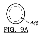
通常、変形可能領域113の変形(すなわち、動力による拡張又は後退)は、触覚面111での触覚フィードバック及び触覚誘導を可能にするように機能する。変形可能領域113の変形は、触覚面111の領域に関連した入力又はコマンドのタイプを示すように機能することができる。変形可能領域113は、拡張設定において、(1)ユーザが押した時にセンサ140への入力を信号で送信する凸状ボタン、(2)ユーザによる変形に沿った複数のポイントで押すことができ、かつ、センサ140上での複数の入力の位置を信号で送信する凸状スライダ、及び/又は、(3)センサ上での複数の入力の位置を信号で送信する凸状ポインティングスティック、を規定することができる。変形可能領域113は、後退設定において、同様に、(1)凹状ボタン、(2)凹状スライダ、及び/又は、(3)凹状ポインティングスティックを規定することができる。凸状ボタンは、図9A及び図9Bに示すように、ドーム形状、円筒形状(すなわち、平坦な上面を有する)、ピラミッド形状又は円錐台形状、立方体形状(すなわち、平坦な上部を有する)、又は、任意の他の適切なボタン形状を規定することができる。以下で説明するように、センサ140は、ボタンを規定する変形可能領域113の触覚面111上での入力(例えば図9A、図10A、図11A及び図12Aに示す入力145)として認識することができる。凸状スライダは、細長い突起部(図10A及び図10Bに示す)、リング(図11A及び図11Bに示す)、十字形の突起部、又は、任意の他の適切な形状の突起部又はスライダを規定することができる。以下で説明するように、センサ140は、スライダを横切る様々な位置でのユーザ入力を識別することができ、かつ、異なるタイプの入力を用いたそれらの位置での入力を区別することができる。一例では、環状形状を規定するスライダが、第2世代のアップル社のiPodの「クリックホイール」として機能することができる。ボタンのようなポインティングスティック(又はポインティングオブジェクト)が、図12A及び図12Bに示すようなドーム形状、円筒形状(すなわち、平坦な上面を有する)、ピラミッド形状、立方体形状(すなわち、平坦な上部を有する)、又は、任意の他の適切なボタン形状を規定することができる。センサ140は、ポインティングスティックに沿った様々な位置でのユーザ入力を識別することができ、かつ、これらのユーザ入力を異なる命令又は機能として区別する。一例では、ポインティングスティックがドーム形状のポインティングスティックを規定する一実施において、右上四分円の近位におけるポインティングスティックの押し下げは、右下四分円の近位におけるポインティングスティックの押し下げとは異なるように解釈され得る。センサ140は、例えば右上四分円から右下四分円への「スイープ」などのさっと掃くような動作におけるポインティングスティックの押し下げを検知することができ、さっと掃くような動作は、第2世代のアップル社のiPodの「クリックホイール」のものと同様の動く入力として解釈され得る。   Typically, deformation of the deformable region 113 (ie, power expansion or retraction) functions to allow haptic feedback and haptic guidance on the haptic surface 111. The deformation of the deformable area 113 can function to indicate the type of input or command associated with the area of the haptic surface 111. In the extended setting, the deformable region 113 can be pressed at (1) a convex button that transmits an input to the sensor 140 as a signal when pressed by the user, and (2) at a plurality of points along the deformation by the user, In addition, a convex slider that transmits a plurality of input positions on the sensor 140 as a signal and / or (3) a convex pointing stick that transmits a plurality of input positions on the sensor as a signal are defined. be able to. The deformable region 113 can similarly define (1) a concave button, (2) a concave slider, and / or (3) a concave pointing stick in the retract setting. The convex buttons can be dome-shaped, cylindrical (i.e. having a flat top), pyramid or frustoconical, cube-shaped (i.e. having a flat top), as shown in Figs. 9A and 9B, or Any other suitable button shape can be defined. As will be described below, the sensor 140 may be recognized as an input on the tactile surface 111 of the deformable region 113 that defines the button (eg, the input 145 shown in FIGS. 9A, 10A, 11A, and 12A). it can. The convex slider can be an elongated projection (shown in FIGS. 10A and 10B), a ring (shown in FIGS. 11A and 11B), a cross-shaped projection, or any other suitable shaped projection or slider. Can be prescribed. As described below, the sensor 140 can identify user input at various positions across the slider and can distinguish input at those positions using different types of inputs. In one example, a slider that defines an annular shape can function as a “click wheel” for a second-generation Apple iPod. A pointing stick (or pointing object) such as a button has a dome shape, a cylindrical shape (ie, having a flat top surface), a pyramid shape, a cubic shape (ie, a flat top portion) as shown in FIGS. 12A and 12B ) Or any other suitable button shape can be defined. The sensor 140 can identify user inputs at various locations along the pointing stick and distinguish these user inputs as different commands or functions. In one example, in one implementation where the pointing stick defines a dome-shaped pointing stick, the pointing stick depressing proximal to the upper right quadrant is different from the pointing stick depressing proximal to the lower right quadrant. Can be interpreted. The sensor 140 can detect the depression of the pointing stick in a quick sweep operation such as a “sweep” from the upper right quadrant to the lower right quadrant, for example. It can be interpreted as a moving input similar to that of Apple's ipod “click wheel”.

ユーザインターフェース100のセンサ140は、一連の検出素子を含んでおり、一連の検出素子のうちの各検出素子は、触覚層110の一部にまたがる容量値を検出するように構成されている。通常、センサ140は、容量式センサ技術を実装しており、変形可能領域113の触覚層111を含む触覚層111上の様々な位置での入力を検知する。センサ140は、触覚層111上での指又はスタイラスペンの接触の存在、拡張設定での変形可能領域113の押し下げ、及び/又は、任意の他の適切なタイプの入力の存在を検知することができる。センサ140は、入力の方向、入力の位置、入力が変形可能領域113に適用される割合、入力が変形可能領域113を内側に変形させるレベル、ユーザ入力のタイプ(例えば、指による入力、スタイラスペンによる入力)などを検知することができる。   The sensor 140 of the user interface 100 includes a series of detection elements, and each detection element of the series of detection elements is configured to detect a capacitance value that spans a portion of the haptic layer 110. Typically, the sensor 140 implements capacitive sensor technology and detects input at various positions on the haptic layer 111 including the haptic layer 111 in the deformable region 113. The sensor 140 may detect the presence of finger or stylus pen contact on the tactile layer 111, the depression of the deformable region 113 in an expanded setting, and / or the presence of any other suitable type of input. it can. The sensor 140 includes an input direction, an input position, a rate at which the input is applied to the deformable region 113, a level at which the input deforms the deformable region 113 inward, and a user input type (eg, finger input, stylus pen). Can be detected.

センサ140は、触覚層110の一部にわたる電界(電磁場)の変動を検知するために協働する少なくとも2つの導体を含む容量センサであってよく、電界は、センサ140の少なくとも2つの導体(すなわち導電パッド)から発せられる。電界の変動は、指又はスタイラスペンによる接触、変形可能領域113の変形、基材118及び/又は空洞内での流体の量又は流体の位置の変化の結果であり得る。   The sensor 140 may be a capacitive sensor that includes at least two conductors that cooperate to sense a variation in the electric field (electromagnetic field) across a portion of the haptic layer 110, and the electric field may be at least two conductors of the sensor 140 (ie, Emitted from a conductive pad). The variation in the electric field may be the result of contact with a finger or stylus pen, deformation of the deformable region 113, changes in the amount of fluid or the position of the fluid in the substrate 118 and / or cavity.

センサ140は、触覚面111上の様々な位置での入力を検知するように構成された任意の数の検出素子を含み得る。各検出素子は、1つの導電パッドを含む表面容量検出素子であってよく、触覚面111の近位での入力の実施(例えば指)が導電パッドから電荷を吸収する。代替的に、各検出素子は、2以上の隣接する導電パッドを含む投影型容量センサであってよく、2以上の導電パッドは、経時変化する電圧によって駆動されて、導電パッドにまたがる電圧を経時で上昇又は低下させ、導電パッド同士の間の容量結合に関連した電圧の立ち上がり時間及び/又は減衰時間を生じさせ、触覚面111上の入力は導電パッド同士の間の容量結合に影響する。しかしながら、各検出素子は、任意の他のタイプの検出素子、電極、導体などであってよい。   The sensor 140 may include any number of detection elements configured to sense input at various locations on the haptic surface 111. Each sensing element may be a surface capacitive sensing element that includes one conductive pad, and an input implementation (eg, a finger) proximal to the haptic surface 111 absorbs charge from the conductive pad. Alternatively, each sensing element may be a projected capacitive sensor that includes two or more adjacent conductive pads, where the two or more conductive pads are driven by a time-varying voltage to cause a voltage across the conductive pad to age. To increase or decrease the voltage, causing rise and / or decay times of the voltage associated with capacitive coupling between the conductive pads, and the input on the haptic surface 111 affects the capacitive coupling between the conductive pads. However, each detection element may be any other type of detection element, electrode, conductor or the like.

一実施において、センサ140は、第1組の平行電極の第1層と、第2組の平行電極の第2層と、を含む投影型容量触覚センサを含み、第2層は、垂直距離だけ第1層からずれ、第2組の電極は第1組の電極を二等分する。この例の実施において、第1組の平行電極内の各電極及び第2組の平行電極の各電極は、複数の導電パッドを規定することができ、第1組の平行電極の導電パッド及び第2組の平行電極の隣接した導電パッドは協働して検出素子を規定する。導電パッドは、四角形、直線的又は任意の他の形状を有してもよく、若しくは、基材118、触覚層110、基材118に隣接するディスプレイ、又は、ユーザインターフェース100の任意の他の構成要素又は関連した装置にまたがって均一な分布でパターニングされてもよい。代替的に、導電パッドは、変形可能領域113の近位において導電パッドが高い分布を有し、かつ、周辺領域115に近位において導電パッドが相対的に低い分布を有する不均一な分布でパターニングされてもよい。同様に、導電パッドは、変形可能領域113の近位において導電パッドがより大きな総表面積を有し、かつ、周辺領域115の近位において導電パッドが相対的により小さな総表面積を有する不均一の分布でパターニングされ得る。一例の実施において、センサ140は、基材118に結合された第1検出素子及び第2検出素子を含み、第1検出素子は空洞125の一部にわたって容量値を検出し、第2検出素子は周辺領域115の一部にわたって容量値を検出する。例えば、第1検出素子は、帯電電圧、電荷電流、帯電時間、放電時間、変形可能領域113に近位の基材118上に配列された第1導電パッド及び第2導電パッドにまたがる通信周波数の少なくとも1つを検出することができる。しかしながら、センサ140は、触覚面111の近位で任意の他の方法でパターニングされて、任意の他の方法で任意の他の容量値を検出するように構成された、任意の他の数の導電パッドを含み得る。   In one implementation, the sensor 140 includes a projected capacitive tactile sensor that includes a first layer of a first set of parallel electrodes and a second layer of a second set of parallel electrodes, the second layer being a vertical distance only. Deviating from the first layer, the second set of electrodes bisects the first set of electrodes. In the implementation of this example, each electrode in the first set of parallel electrodes and each electrode in the second set of parallel electrodes can define a plurality of conductive pads, and the conductive pads of the first set of parallel electrodes and the first set of parallel electrodes. Adjacent conductive pads of two sets of parallel electrodes cooperate to define a sensing element. The conductive pads may have a square shape, a straight line, or any other shape, or the substrate 118, the tactile layer 110, the display adjacent to the substrate 118, or any other configuration of the user interface 100. It may be patterned with a uniform distribution across the elements or associated devices. Alternatively, the conductive pads are patterned with a non-uniform distribution in which the conductive pads have a high distribution proximal to the deformable region 113 and the conductive pads have a relatively low distribution proximal to the peripheral region 115. May be. Similarly, the conductive pads have a non-uniform distribution where the conductive pads have a greater total surface area proximal to the deformable region 113 and the conductive pads have a relatively smaller total surface area proximal to the peripheral region 115. Can be patterned. In one example implementation, sensor 140 includes a first sensing element and a second sensing element coupled to substrate 118, the first sensing element detecting a capacitance value over a portion of cavity 125, wherein the second sensing element is The capacitance value is detected over a part of the peripheral region 115. For example, the first sensing element may have a charging voltage, a charge current, a charging time, a discharging time, a communication frequency spanning a first conductive pad and a second conductive pad arranged on the substrate 118 proximal to the deformable region 113. At least one can be detected. However, the sensor 140 may be patterned in any other manner proximal to the haptic surface 111 and configured to detect any other capacitance value in any other manner. A conductive pad may be included.

容量性触覚センサであるセンサ140の導電パッド(例えば第1導体)は、銅、マイクロワイヤ又はナノワイヤ、若しくは、インジウムスズ酸化物(ITO)などの透明な導体であってよい。例えば、基材118は、両方の幅広面にわたってマスクされて、ITOが両方の幅広面にスパッタリングされて導電パッドの均一な密度又は可変の密度を有する垂直電極を形成してもよい。しかしながら、センサ140の導電パッドは任意のタイプの導電金属(又は導電流体)を含み得る。   The conductive pad (eg, first conductor) of sensor 140, which is a capacitive tactile sensor, may be a transparent conductor such as copper, microwire or nanowire, or indium tin oxide (ITO). For example, the substrate 118 may be masked across both wide surfaces and ITO may be sputtered onto both wide surfaces to form vertical electrodes having a uniform or variable density of conductive pads. However, the conductive pads of the sensor 140 can include any type of conductive metal (or conductive fluid).

容量性触覚センサを含むセンサ140は、触覚面111上に又は触覚面111に隣接して指、スタイラスペン又は他の器具の存在に加えて、変形可能領域113の触覚面111の高さを検出するようにさらに機能することができる。図14Aに示すように、第1導体(例えば第1導電パッド)は、変形可能領域113の内側への変形が第1導体に対する空洞125内の流体の高さを変化させることによって容量センサで検出される静電容量に影響を及ぼすように、空洞125内に又は空洞125に隣接して配列され得る。例えば、第1導体は、触覚面111とは反対側の空洞125の底部上に配列されてよく、それによって、容量センサは、変形可能領域113が拡張、後退及び/又は入力に応答して内側に変形する際に流体の高さ変動を検出することができる。代替的に、第1導体は、触覚層110の背面内に又は背面上に配列されてもよく、その結果、変形可能領域113が、拡張、後退及び/又は入力によって変形させられる際に第1導体が特定の表面とともに変形し、それによって空洞125内の流体の高さ変動の検出を可能にする。しかしながら、第1導体は、空洞125、基材118又は触覚層110内の又はこれらに隣接した任意の適切な場所に配列されてもよい。   Sensor 140, including a capacitive tactile sensor, detects the height of tactile surface 111 in deformable region 113 in addition to the presence of a finger, stylus pen or other instrument on or adjacent to tactile surface 111. Can function further to do. As shown in FIG. 14A, the first conductor (eg, the first conductive pad) is detected by the capacitive sensor by the deformation inward of the deformable region 113 by changing the height of the fluid in the cavity 125 with respect to the first conductor. May be arranged in or adjacent to the cavity 125 to affect the capacitance that is applied. For example, the first conductor may be arranged on the bottom of the cavity 125 opposite the haptic surface 111 so that the capacitive sensor can be deformed inwardly in response to the expansion, retraction and / or input of the deformable region 113. It is possible to detect the fluctuation of the height of the fluid when it is deformed into the shape. Alternatively, the first conductor may be arranged in or on the back surface of the haptic layer 110 such that the first region when the deformable region 113 is deformed by expansion, retraction and / or input. The conductor deforms with a particular surface, thereby allowing detection of fluid height variations in the cavity 125. However, the first conductor may be arranged in any suitable location within or adjacent to the cavity 125, the substrate 118, or the tactile layer 110.

図14Bに示すように、容量性タッチは、空洞125内に配列された第2導体を含み得る。第2導体144は、変形可能領域113に入力が加えられると、第1導体及び第2導体144にわたる静電容量の変化を検知することができる。例えば、ユーザが変形可能領域113を内側に変形させると、第1導体と第2導体144との間にある流体の量及び/又は流体の高さが変化し、第1導体と第2導体144との間で検出される静電容量の変化を生じさせる。第1導体と第2導体144との間の高低差の勾配が、第1導体と第2導体144との間の静電容量の測定可能な変化をさらに生じさせ得る。例えば、変形可能領域113上の入力が第1導体と第2導体との間の距離を減少させ、それによって、第2導体144によって読み出される静電容量を変化させる。この変化は、変形可能領域113の形状に対する入力の場所の特定を容易にし得る。   As shown in FIG. 14B, the capacitive touch may include second conductors arranged in the cavity 125. When an input is applied to the deformable region 113, the second conductor 144 can detect a change in capacitance across the first conductor and the second conductor 144. For example, when the user deforms the deformable region 113 inward, the amount of fluid and / or the height of the fluid between the first conductor and the second conductor 144 changes, and the first conductor and the second conductor 144 change. A change in capacitance detected between and. The elevation gradient between the first conductor and the second conductor 144 may further cause a measurable change in capacitance between the first conductor and the second conductor 144. For example, an input on the deformable region 113 reduces the distance between the first conductor and the second conductor, thereby changing the capacitance read by the second conductor 144. This change may facilitate identification of the input location for the shape of the deformable region 113.

第2導体144は、第1導体と協力して、空洞125内の高さ変動のさらに局部的な容量測定を生じさせる第2導体144の上方の領域内の流体の高さ変動を検出することができる。2つの検出素子による空洞125内での局部的な静電容量の変化の測定は、流体の相対的な高低差を測定することを可能にし得る。例えば、入力が変形可能領域113を変形させる時、第1導体上の流体の高さは第2導体上の流体の高さと異なり、その結果、第1導体の検出された容量値と、第2導体144の検出された容量値との差分を生じさせる。第1導体と第2導体144の第1部分との間の静電容量が第1導体と第2導体144の第2部分との間の静電容量と比較されて、流体の高さの相対的な差分を特定する。2つの導体同士の間の容量値の相対的な差分は、従って、変形可能領域113の形状に対する入力の場所の特定を容易にし得る。第2導体144の第1部分及び第2部分は、第2導体144に沿って連続した区画であり得るが、代替的に、第1部分及び第2部分とは異なる材料の第3部分によって、又は、第2導体144の裂け目によって、分離され得る。第2導体144は、材料及び製造工程において第1導体と同一であり得るが、第1導電パッド及び第2導電パッドは、任意の他の同様の又は異なる材料、形状又は配置を有してもよい。   The second conductor 144 cooperates with the first conductor to detect fluid height variations in the region above the second conductor 144 that causes a more localized capacitance measurement of the height variation in the cavity 125. Can do. Measurement of the local capacitance change in the cavity 125 by the two sensing elements may allow the relative height difference of the fluids to be measured. For example, when the input deforms the deformable region 113, the height of the fluid on the first conductor is different from the height of the fluid on the second conductor, so that the detected capacitance value of the first conductor and the second A difference from the detected capacitance value of the conductor 144 is generated. The capacitance between the first conductor and the first portion of the second conductor 144 is compared with the capacitance between the first conductor and the second portion of the second conductor 144 to determine the relative height of the fluid. Specific differences are identified. The relative difference in capacitance values between the two conductors can thus facilitate the identification of the input location relative to the shape of the deformable region 113. The first portion and the second portion of the second conductor 144 may be a continuous section along the second conductor 144, but alternatively by a third portion of material different from the first portion and the second portion, Alternatively, it can be separated by a tear in the second conductor 144. The second conductor 144 may be the same as the first conductor in material and manufacturing process, but the first conductive pad and the second conductive pad may have any other similar or different material, shape or arrangement. Good.

図14C及び図14Dに示すように、容量触覚センサを含むセンサ140は第3導体及び/又は第4導体を含み得る。第3導体及び/又は第4導体は、変形可能領域113の近位に配列されてもよく、及び従って、変形可能領域113に近位のより正確な入力検知を可能にする。例えば、(図14Dに示す)変形可能領域113に近位の4つの導体を含むセンサ140に関して、変形可能領域113は、変形可能領域113の中心に近位の原点を有するX軸及びY軸によって四象眼座標系に分割され得る。この例において、変形可能領域113の形状に対する入力の場所は様々な方法で測定され得る。図15Aに示す一例の実施では、静電容量及び/又は第1導体と第3導体146との間の相対的な静電容量が、X軸に沿った入力の場所を特定するために測定され、静電容量及び/又は第2導体144と第4導体148との間の相対的な静電容量が、Y軸に沿った入力の場所を特定するために測定される。測定されたX軸入力とY軸入力との場所は、四象眼座標系上での入力の場所を特定するために使用され得る。図15に示す別の例の実施では、3つの静電容量及び/又は相対的な容量値が、第1導体と第2導体144との間、第1導体と第3導体146との間、第1導体と第4導体148との間で測定される。3つの容量値は、(「tridrant」座標系に重ねられ得る)四象眼座標系内における入力の場所を特定するために用いられ得る。しかしながら、センサ140は、任意の他の適切な方法で、変形可能領域及び/又は周辺領域の近位の入力を検知するよう、変形可能領域113に近位の又は離れた任意の他の数の導体を含み得る。   As shown in FIGS. 14C and 14D, a sensor 140 including a capacitive tactile sensor may include a third conductor and / or a fourth conductor. The third and / or fourth conductors may be arranged proximal to the deformable region 113 and thus allow for more accurate input sensing proximal to the deformable region 113. For example, with respect to sensor 140 that includes four conductors proximal to deformable region 113 (shown in FIG. 14D), deformable region 113 is defined by an X-axis and a Y-axis having a proximal origin in the center of deformable region 113. It can be divided into a quadrant coordinate system. In this example, the input location for the shape of the deformable region 113 can be measured in various ways. In the example implementation shown in FIG. 15A, the capacitance and / or the relative capacitance between the first conductor and the third conductor 146 are measured to identify the location of the input along the X axis. , The capacitance and / or the relative capacitance between the second conductor 144 and the fourth conductor 148 is measured to identify the location of the input along the Y axis. The measured location of the X-axis input and the Y-axis input can be used to identify the location of the input on the quadrant coordinate system. In another example implementation shown in FIG. 15, three capacitances and / or relative capacitance values are between the first conductor and the second conductor 144, between the first conductor and the third conductor 146, Measured between the first conductor and the fourth conductor 148. The three capacitance values can be used to identify the location of the input in the quadrant coordinate system (which can be overlaid on the “tridrant” coordinate system). However, the sensor 140 may be in any other suitable manner and any other number of proximal or remote to the deformable region 113 to sense the proximal input of the deformable region and / or the peripheral region. A conductor may be included.

図16Aに示すように、第1導体、第2導体144、第3導体などは、空洞125に対して第1レベルで配列され得る。代替的に、図16Bに示すように、第1導体は空洞125に対して第1レベルで配列され、第2導体144は空洞125に対して第2レベルで配列され得る。第3導体、第4導体、及び/又は、任意の他の適切な数の導体が、空洞125に対して第2レベル又は他のレベルで配列され得る。空洞125に対して様々な高さで空洞125内で導体を配置することによって、入力の場所及び大きさの検知を容易にし得る。追加的に又は代替的に、図16Cに示すように、第1導体は、基材118上に又は基材118内に配列されてよく、及び、第2導体144は触覚層110内に配列されてよい。しかしながら、センサ140は、導体の任意の他の組み合わせ又は配列を含み得る。   As shown in FIG. 16A, the first conductor, the second conductor 144, the third conductor, etc. may be arranged at a first level relative to the cavity 125. Alternatively, as shown in FIG. 16B, the first conductor may be arranged at a first level relative to the cavity 125 and the second conductor 144 may be arranged at a second level relative to the cavity 125. A third conductor, a fourth conductor, and / or any other suitable number of conductors may be arranged at the second level or other level relative to the cavity 125. By placing conductors in the cavity 125 at various heights relative to the cavity 125, sensing the location and size of the input can be facilitated. Additionally or alternatively, as shown in FIG. 16C, the first conductor may be arranged on or in the substrate 118 and the second conductor 144 is arranged in the haptic layer 110. It's okay. However, the sensor 140 may include any other combination or arrangement of conductors.

図17A及び図17Bに示すように、容量触覚センサを含むセンサ140は、第1導体及び第2導体を通じた変形可能領域の高さ変動を検出することができる。この実施において、ユーザが変形可能領域113を内側に変形させる時に移動する場所に第1導体が配列され、ユーザが変形可能領域113を内側に変形させる時に相対的に固定されたままの場所に第2導体144が配列され得る。第2導体144は、図17Aに示すように、空洞125内に配列されてよく、又は、図17Bに示すように、ユーザインターフェース100内の相対的に固定された場所に配列されてよい。この実施において、第1導体と第2導体との間の距離の変化は、第1導体と第2導体との間で測定された静電容量を変化させ、その変化が入力を示す。第1導体は、変形可能領域113の内側への変形が第1導体を同様に変形させるように、可撓性を有する導体であってよい。第1導体の動きは、第1導体と第2導体144との間の容量値、及び、第1導体と第3導体146との間の容量値を測定することによって検知され得る。これらの容量値の間の差分は、従って、変形可能領域113に対する入力の場所を示し得る。代替的に、第1導体と第2導体144の第1部分との間の容量値が、第1導体と第2導体の144の第2部分との間の容量値と比較されて、流体の高さの相対的な差分を特定する。従って、2つの導体間の容量値の相対的な差分は、変形可能領域113に対する入力の場所の特定を容易にし得る。第2導体144は、変形可能領域113の周辺の近くに、変形可能領域113の中心の近くに、又は、任意の他の適切な場所に配列され得る。代替的に、図18D及び図18Eに示すように、第2導体144は、第1導体に対して垂直に配列されて、第1導体の軸に沿って及び第2導体144の軸に沿って変形が検知されることを可能にし、それによって、センサ感度を高めている。   As shown in FIGS. 17A and 17B, the sensor 140 including the capacitive tactile sensor can detect the height variation of the deformable region through the first conductor and the second conductor. In this implementation, the first conductor is arranged in a place where the user moves when deforming the deformable area 113 inward, and the first conductor is placed in a relatively fixed place when the user deforms the deformable area 113 inward. Two conductors 144 may be arranged. The second conductor 144 may be arranged in the cavity 125 as shown in FIG. 17A, or may be arranged in a relatively fixed location in the user interface 100 as shown in FIG. 17B. In this implementation, a change in the distance between the first conductor and the second conductor changes the capacitance measured between the first conductor and the second conductor, and the change indicates an input. The first conductor may be a flexible conductor so that deformation inward of the deformable region 113 causes the first conductor to similarly deform. The movement of the first conductor can be detected by measuring the capacitance value between the first conductor and the second conductor 144 and the capacitance value between the first conductor and the third conductor 146. The difference between these capacitance values can thus indicate the location of the input to the deformable region 113. Alternatively, the capacitance value between the first conductor and the first portion of the second conductor 144 is compared with the capacitance value between the first conductor and the second portion of the second conductor 144 to determine the amount of fluid. Identify relative height differences. Therefore, the relative difference in the capacitance value between the two conductors can facilitate the identification of the input location for the deformable region 113. The second conductor 144 may be arranged near the periphery of the deformable region 113, near the center of the deformable region 113, or at any other suitable location. Alternatively, as shown in FIGS. 18D and 18E, the second conductor 144 is arranged perpendicular to the first conductor, along the axis of the first conductor and along the axis of the second conductor 144. It allows deformation to be detected, thereby increasing sensor sensitivity.

従って、図18に示すように、容量触覚センサを含むセンサ140は、例えば基材118にまたがってパターニングされた導電パッド、触覚層110にまたがってパターニングされた導電パッド、及び/若しくは、空洞125上又は空洞125内に配列された導電パッドの形態などの複数の導体を含み得る。図18Aに示すように、導電パッドは、同一の又は同様のサイズ及び/又は形状を有してもよい。代替的に、図18B〜図18Eに示すように、導電パッドは、例えば変形可能領域113への近さに基づき、異なる又は同様ではないサイズ、形状及び/又は外形を有してもよい。例えば、1つの導電パッドが、図18B及び図18Cに示すように、空洞125及び/又は変形可能領域113の配置に従った配置を規定し得る。しかしながら、第1導体及び第2導体の任意の適切な配列又は配置が用いられてもよい。   Accordingly, as shown in FIG. 18, the sensor 140 including a capacitive tactile sensor may include a conductive pad patterned across the substrate 118, a conductive pad patterned across the tactile layer 110, and / or on the cavity 125. Or it may include a plurality of conductors, such as in the form of conductive pads arranged within the cavity 125. As shown in FIG. 18A, the conductive pads may have the same or similar size and / or shape. Alternatively, as shown in FIGS. 18B-18E, the conductive pads may have different or not similar sizes, shapes and / or outlines, for example based on proximity to the deformable region 113. For example, one conductive pad may define an arrangement according to the arrangement of the cavity 125 and / or the deformable region 113 as shown in FIGS. 18B and 18C. However, any suitable arrangement or arrangement of first and second conductors may be used.

上述したように、センサ140は、第1組の平行電極140Xの第1層と、第2組の平行電極140Yの第2層と、を含む投影型容量触覚センサを含んでよく、第2層はいくらかの垂直距離だけ第1層からずれ、かつ、図26に示すように、第2組の電極は第1組の電極に直角に交差する。この実施において、電極は、触覚層110の下方に配列されてよく、及び、図24A〜図24Dに示すように、触覚層110に通じて広がる電界を発生させるように構成され得る。通常、この実施では、フィールド電極(例えば第1導体)は電界を発生させることができ、及び、対のセンサ電極(例えば第2導体)は容量結合を通じて電界を検知することができ、及び、プロセッサ160は、フィールド電極と対のセンサ電極との間の容量結合の大きさの変化を触覚面111上での入力として特徴づけることができる。電極は、触覚層110と反対側の基材118に隣接して配列され、基材118内(例えば図24Aに示すように、流体チャネル138内及び/又は空洞125内)に配列され、又は、ユーザインターフェース100内のどこかに配列され得る。触覚層110及び/又はある量の流体は、触覚層110及び/又は流体が、拡張設定の空洞125及び/又は触覚層110を電界が貫通することを促進することができるように、空気とは異なった誘電体であり得る。従って、流体、触覚層の材料及び又は基材の材料は、後退設定及び拡張設定の触覚層110の全域の電界の分布を最適化するために、その磁気的特性及び/又はその電気的特性に基づいて選択され得る。追加的に又は代替的に、センサ140は、電荷移動又は表面容量触覚センサを含んでよく、電荷(すなわち電子)が、電極(例えば導電パッド)と指、スタイラスペン、又は、触覚層110に接触する他のタッチ器具との間で伝達される。しかしながら、センサ140は、任意の他の適切なタイプの容量触覚センサであってもよい。   As described above, the sensor 140 may include a projected capacitive tactile sensor that includes a first layer of a first set of parallel electrodes 140X and a second layer of a second set of parallel electrodes 140Y. Deviation from the first layer by some vertical distance, and the second set of electrodes intersects the first set of electrodes at right angles, as shown in FIG. In this implementation, the electrodes may be arranged below the haptic layer 110 and may be configured to generate an electric field that extends through the haptic layer 110 as shown in FIGS. 24A-24D. Typically, in this implementation, the field electrode (eg, the first conductor) can generate an electric field, and the pair of sensor electrodes (eg, the second conductor) can sense the electric field through capacitive coupling, and the processor 160 can characterize the change in magnitude of capacitive coupling between the field electrode and the pair of sensor electrodes as an input on the haptic surface 111. The electrodes are arranged adjacent to the substrate 118 opposite the tactile layer 110 and arranged in the substrate 118 (eg, in the fluid channel 138 and / or in the cavity 125 as shown in FIG. 24A), or It can be arranged somewhere within the user interface 100. The haptic layer 110 and / or a quantity of fluid may be defined as air so that the haptic layer 110 and / or fluid may facilitate an electric field to penetrate the extended setting cavity 125 and / or the haptic layer 110. It can be a different dielectric. Thus, the fluid, haptic layer material, and / or substrate material may have its magnetic properties and / or its electrical properties to optimize the electric field distribution across the haptic layer 110 in the retracted and extended settings. Can be selected based on. Additionally or alternatively, the sensor 140 may include a charge transfer or surface capacitive tactile sensor, where the charge (ie, electrons) contacts the electrodes (eg, conductive pads) and the finger, stylus pen, or tactile layer 110. To communicate with other touch devices. However, the sensor 140 may be any other suitable type of capacitive tactile sensor.

さらに、図24A〜図24Dに示すように、触覚層110及び/又はある量の流体120は、空洞125及び/又は触覚層を通じて電界をさらに集中させる磁気の、金属の又は偏極した素子又はイオン117を包含してよく、この素子又はイオン117は、拡張設定における触覚面111上の入力に対するセンサ140の感度を向上させることができる。一例では、ある量の流体120は、溶液中のマイクロスケール又はナノスケールの金属粒子を含有する。別の例では、触覚層110は、空洞125内に延びる列であって、磁気の、金属の又は偏極の素子又はイオンを組み込んだ列を含む。さらに別の例では、触覚層110は、実質的に均一な厚さであり、触覚層110内に注入された磁気の、金属の又は偏極の素子又はイオン117を含む。この例では、図24Aに示すように、磁気の、金属の又は偏極の素子又はイオン117は、変形可能領域113に局部的に集中されてよく、触覚層110の全域で実質的に不均一に分散されてもよく、又は、任意の他の方法で触覚層110内に配列されてもよい。さらに別の例では、触覚層110は、触覚層110の背面及び触覚面111の少なくとも1つにわたって磁気の、金属の又は偏極のストリップを含み得る。しかしながら、磁気の、金属の又は偏極の素子又はイオンは、ユーザインターフェース100内で他の方法で配列されてもよい。   Further, as shown in FIGS. 24A-24D, the haptic layer 110 and / or a quantity of fluid 120 may cause a magnetic, metallic or polarized element or ion that further concentrates the electric field through the cavity 125 and / or the haptic layer. 117, which may increase the sensitivity of the sensor 140 to input on the haptic surface 111 in an extended setting. In one example, an amount of fluid 120 contains microscale or nanoscale metal particles in solution. In another example, haptic layer 110 includes a row that extends into cavity 125 and incorporates a magnetic, metallic or polarized element or ion. In yet another example, haptic layer 110 has a substantially uniform thickness and includes magnetic, metallic or polarized elements or ions 117 implanted into haptic layer 110. In this example, as shown in FIG. 24A, magnetic, metallic or polarized elements or ions 117 may be concentrated locally in the deformable region 113 and are substantially non-uniform across the haptic layer 110. Or may be arranged in the haptic layer 110 in any other manner. In yet another example, the haptic layer 110 may include a magnetic, metallic or polarized strip across at least one of the back surface of the haptic layer 110 and the haptic surface 111. However, magnetic, metallic or polarized elements or ions may be arranged in other ways within the user interface 100.

一例の実施では、センサ140は、触覚面111に近位の指、スタイラスペン又は他のタッチ器具の存在によって、触覚層110の全域の電界の分布の変化である入力を検知する。例えば、図24B及び図24Cに図示するもののように、センサ140は電界の変化を検知することができる。別の例の実施では、図24A及び図24Bに図示するもののように、触覚層110内の磁気の、金属の又は偏極の素子又はイオン若しくはある量の流体120が電界の分布を破壊する一方で電界を通って移動する際に、センサ140は触覚層110の位置の変化を検知する。この例の実施では、従って、センサ140は、指、スタイラスペン又は他のタッチ器具の存在を直接検知するよりも、むしろ触覚層110及び/又は流体の動きを検知することができる。   In one example implementation, the sensor 140 detects an input that is a change in the distribution of the electric field across the haptic layer 110 due to the presence of a finger, stylus pen, or other touch device proximal to the haptic surface 111. For example, as shown in FIGS. 24B and 24C, the sensor 140 can detect changes in the electric field. In another example implementation, as illustrated in FIGS. 24A and 24B, a magnetic, metallic or polarized element or ion or some amount of fluid 120 in the haptic layer 110 destroys the electric field distribution. As the sensor 140 moves through the electric field, the sensor 140 detects a change in the position of the haptic layer 110. In this example implementation, therefore, sensor 140 can detect movement of haptic layer 110 and / or fluid rather than directly detecting the presence of a finger, stylus pen or other touch device.

センサ140が投影型容量センサである一実施では、センサ140は様々なモードで機能し得る。変形可能領域113が後退設定にある時、センサ140は、触覚層110にわたって実質的に均一な電界を発生させることによって第1モードで動作する。変形可能領域113が拡張設定にある時、センサ140は、触覚層110にわたって不均一な電界を発生させることによって第2モードで動作することができる。第2モードでは、センサ素子間の容量結合は変形可能領域113の近位でより強くなるが、そうでない場合には、第1モードと第2モードとの間の触覚層110にわたる他の場所で変化しない。例えば、変形可能領域113での電界の大きさは、変形可能領域113に近位の2つの隣接する電極にわたる電位差を増大させることによって増大し得る。代替的に、触覚層110の他の部分での電界の大きさは低減されてよく、そのことによって、触覚層110の他の部分での入力感度を下げる一方で、変形可能領域113での入力感度を実質的に維持することができる。同様に、センサ140は、入力が変形可能領域113でのみ検出されるように、変形可能領域113の外側の触覚層110の部分で電界の発生を抑制することができる。   In one implementation where sensor 140 is a projected capacitive sensor, sensor 140 may function in various modes. When the deformable region 113 is in the retracted setting, the sensor 140 operates in the first mode by generating a substantially uniform electric field across the haptic layer 110. When the deformable region 113 is in the expanded setting, the sensor 140 can operate in the second mode by generating a non-uniform electric field across the haptic layer 110. In the second mode, capacitive coupling between the sensor elements is stronger near the deformable region 113, otherwise it is elsewhere in the haptic layer 110 between the first mode and the second mode. It does not change. For example, the magnitude of the electric field at the deformable region 113 can be increased by increasing the potential difference across two adjacent electrodes proximal to the deformable region 113. Alternatively, the magnitude of the electric field at other parts of the haptic layer 110 may be reduced, thereby reducing input sensitivity at other parts of the haptic layer 110 while input at the deformable region 113. Sensitivity can be substantially maintained. Similarly, the sensor 140 can suppress the generation of an electric field in the portion of the tactile layer 110 outside the deformable region 113 so that the input is detected only in the deformable region 113.

上述の実施では、センサ140は、区別可能なモードで動作することができ、各モードは、変形可能領域113の特定の垂直位置又は設定に関連付けられる。代替的に、センサ140は、完全に後退した設定と完全に拡張した設定の間の変形可能領域の位置の連続体に対してセンサ設定の連続体を規定する様々なモードで動作し得る。しかしながら、投影型容量センサを含むセンサ140は、後退設定と拡張設定とにおける任意の他の方法で機能し得る。さらに、センサ140は、任意の他の適切なタイプのセンサであってよい。   In the implementation described above, the sensor 140 can operate in distinct modes, each mode being associated with a particular vertical position or setting of the deformable region 113. Alternatively, the sensor 140 may operate in various modes that define a continuum of sensor settings relative to a continuum of deformable region positions between a fully retracted setting and a fully expanded setting. However, the sensor 140, including a projected capacitive sensor, can function in any other way in the retract setting and the extended setting. Further, the sensor 140 may be any other suitable type of sensor.

センサ140は、触覚層111にわたる容量値の容量マップ(すなわち、記憶された最初の容量値及び差分値)を出力することができる。例えば、容量マップは、触覚面111の全部又は一部にわたる電界の分布を示すデータを含み得る。触覚面111上での入力の位置(すなわち、XY座標)は、(図26に示す)容量マップを分析することによって特定され得る。入力の大きさ、速度、タイミングなどは、例えば容量マップを以前の容量マップと比較することによって、容量マップから同様に特定され得る。通常、プロセッサ160は、容量マップを分析し、容量マップの変化の重心(例えば質量中心)を確認することができ、及び従って、変化の重心を入力と関連付ける。従って、入力の場所、大きさ、タイミング及び/又は速度のいずれかは、1以上の所定の時間の容量マップに関連付けられ、及び/又は、所定の期間を超える容量マップの変化又は変化のレートに関連付けられる。   The sensor 140 can output a capacitance map of capacitance values across the haptic layer 111 (ie, the stored initial capacitance value and difference value). For example, the capacitance map may include data indicating the distribution of the electric field across all or part of the haptic surface 111. The position of the input on the haptic surface 111 (ie, the XY coordinates) can be determined by analyzing the capacitance map (shown in FIG. 26). The magnitude, speed, timing, etc. of the input can be similarly identified from the capacity map, for example by comparing the capacity map with the previous capacity map. Typically, the processor 160 can analyze the volume map to identify a centroid (eg, center of mass) of the change in the volume map, and thus associates the centroid of change with the input. Thus, any of the input locations, magnitudes, timings and / or speeds are associated with one or more predetermined time capacity maps and / or at a capacity map change or rate of change over a predetermined period of time. Associated.

センサ140は、代替的に、抵抗センサを含み得る。容量センサと同様に、抵抗センサは、少なくとも2つの導体を含んでよく、2つの導体の間の抵抗を検出するように機能することができる。一例では、2つの導体は、空洞125内の2つの異なった場所に配列され得る。2つの導体の間の抵抗は、後退設定の第1値と拡張設定の第2値とを有する。変形可能領域113を内側に変形させる入力に応答して、2つの導体の間の抵抗は、第1値と第2値との間の第3値に適応する。この抵抗値を読み取ることによって、センサ140は、入力、後退した変形可能領域の内側への変形、及び/又は、変形可能領域113の内側への変形の度合いを検知することができる。   The sensor 140 may alternatively include a resistance sensor. Similar to the capacitive sensor, the resistance sensor may include at least two conductors and may function to detect a resistance between the two conductors. In one example, the two conductors can be arranged at two different locations within the cavity 125. The resistance between the two conductors has a first value for the reverse setting and a second value for the extended setting. In response to an input that deforms the deformable region 113 inwardly, the resistance between the two conductors adapts to a third value between the first value and the second value. By reading this resistance value, the sensor 140 can detect the degree of input, deformation inside the retractable deformable area, and / or deformation inside the deformable area 113.

変形可能領域113及び隣接する非変形可能領域にまたがる抵抗センサは均一に検知可能である。例えば、センサ電極のサイズ及び密度は、例えば基材118及び/又は触覚層110をわたって、センサ140の全域で一定であってよい。代替的に、センサ140は、例えば電極のサイズ及び/又は密度を変化させることによって不均一な感度を示し得る。センサ140は、不均一な感度を実装して、様々な設定の変形可能領域113上での入力の検知を可能にし得る。通常、変形可能領域113の触覚層110の有効厚さが、後退設定より拡張設定の方が実質的により大きいものであるので、拡張設定の変形可能領域113の触覚面111上での入力は、センサ140のより大きな面積にわたって分散され、従って、変形可能領域113に隣接する任意の特定の電極でのセンサ信号の大きさを制限し、従って、変形可能領域113に近位で大きな入力感度を必要とする。   A resistance sensor across the deformable region 113 and the adjacent non-deformable region can be detected uniformly. For example, the size and density of the sensor electrodes may be constant across the sensor 140, for example across the substrate 118 and / or the haptic layer 110. Alternatively, the sensor 140 may exhibit non-uniform sensitivity, for example by changing the size and / or density of the electrodes. The sensor 140 may implement non-uniform sensitivity to allow for detection of input on the deformable region 113 with various settings. Usually, since the effective thickness of the tactile layer 110 in the deformable region 113 is substantially larger in the extended setting than in the backward setting, the input on the tactile surface 111 of the deformable region 113 in the extended setting is Distributed over a larger area of the sensor 140, thus limiting the magnitude of the sensor signal at any particular electrode adjacent to the deformable region 113 and thus requiring greater input sensitivity proximal to the deformable region 113 And

追加的に又は代替的に、より広範囲のセンサエリアにわたる変形可能領域113での入力の分散を制限するため、触覚層110及び/又は基材の弾性は不均一であってよい。例えば、触覚層110は、変形可能領域113の中心の近位でより弾性(すなわち可撓性)を有してもよい。この例では、触覚層110は、変形可能領域113の周縁の近位よりも変形可能領域113の中心の近位の断面でより薄くてよい。代替的に、触覚層110の材料の特性は、変形可能領域113にわたって変動してもよく、触覚層110の最も弾性を有する又は最も可撓性を有する部分は変形可能領域113の中心の近位である。この実施では、変形可能領域113の触覚層110の一部が高い弾性を有することによって、センサ140のより狭いエリアにわたって入力の力を集中させることができ、従って、変形可能領域113の近位での入力に対する感度を向上させる。さらに、触覚層110の弾性を変化させることによって、センサ140の特定の電極を順番に活性化させることができ、活性化された電極の数又は順番は、入力を生じさせる変形可能領域113の変位の大きさを示し得る。時間成分と結合されると、活性化された電極の数又は順番は、入力を生じさせる変形可能領域113の変形の速度をさらに示唆する。しかしながら、抵抗センサは、任意の他の方法で機能してよく、触覚層110及び基材は、任意の他の外形又は材料であってよく、前述の機能性を可能にする。   Additionally or alternatively, the elasticity of the haptic layer 110 and / or the substrate may be non-uniform to limit the distribution of input in the deformable region 113 over a wider sensor area. For example, the haptic layer 110 may be more elastic (ie, flexible) proximal to the center of the deformable region 113. In this example, haptic layer 110 may be thinner in the cross section proximal to the center of deformable region 113 than proximal to the periphery of deformable region 113. Alternatively, the material properties of the haptic layer 110 may vary across the deformable region 113 and the most elastic or most flexible portion of the haptic layer 110 is proximal to the center of the deformable region 113. It is. In this implementation, a portion of the haptic layer 110 in the deformable region 113 has a high elasticity so that the input force can be concentrated over a smaller area of the sensor 140, and thus proximal to the deformable region 113. Improve sensitivity to input. Furthermore, by changing the elasticity of the haptic layer 110, specific electrodes of the sensor 140 can be activated in turn, and the number or order of the activated electrodes depends on the displacement of the deformable region 113 that causes the input. Can be shown. When combined with the time component, the number or sequence of activated electrodes further suggests the rate of deformation of the deformable region 113 that causes the input. However, the resistance sensor may function in any other manner, and the haptic layer 110 and the substrate may be any other profile or material, allowing the functionality described above.

図19Aに示すように、センサ140は、追加的に又は代替的に、圧力センサを含み得る。この実施では、ある量の流体120は、空洞125を実質的に満たし、及び、実質的に圧縮性流体であってよく、空洞125は、変形可能領域113の内側への変形に応答して圧力センサが空洞内の圧力の上昇を検出することができるように密閉され得る。圧力センサは、絶対圧力センサ、差圧センサ又は任意の適切なタイプの圧力センサであってよい。圧力センサは、代替的に、空洞125内に装着されて部分的に空洞125を規定する歪みゲージであってよく、歪みゲージは、変形可能領域113の内側への変形に応答して変形する。しかしながら、圧力センサは、変形可能領域113の内側への変形による空洞125内の圧力変化を検出するよう構成された任意の他の適切なタイプであってよい。   As shown in FIG. 19A, the sensor 140 may additionally or alternatively include a pressure sensor. In this implementation, an amount of fluid 120 substantially fills cavity 125 and may be a substantially compressible fluid, where cavity 125 is pressure responsive to inward deformation of deformable region 113. It can be sealed so that the sensor can detect an increase in pressure in the cavity. The pressure sensor may be an absolute pressure sensor, a differential pressure sensor or any suitable type of pressure sensor. The pressure sensor may alternatively be a strain gauge that is mounted within the cavity 125 and partially defines the cavity 125, and the strain gauge deforms in response to the inward deformation of the deformable region 113. However, the pressure sensor may be any other suitable type configured to detect a pressure change in the cavity 125 due to inward deformation of the deformable region 113.

図19Bに示すように、センサ140は、追加的に又は代替的に流量センサを含み得る。流量センサは、変形可能領域113上での入力に応答して流体の方向流を検出することができる。この実施では、空洞125は流体チャネルに結合され得る。変形可能領域113の内側への変形に応答して、空洞125の総容積が減少してチャネルの外側に流体を押し出す。従って、流量センサは、流体チャネル138を通過する流体の流れを検知及び/又は検出して、変形可能領域113の変形及び/又は変形可能領域113の変形の大きさを識別する。流量センサは流体チャネル138に流動的に結合され得る。一例では、チャネルは、通常は閉じられて空洞125内に一定の量の流体を維持するバルブを含んでもよい。変形可能領域113の内側への変形がある時、バルブは開かれ、他のチャネルへの逆流を可能にする。流量センサは、流体の流量を検出する流量率センサであってもよい。チャネルを通って流れる流体120の量は、チャネルの既知の断面積及び流量から計算され得る。例えば、バルブ及び/又はセンサは、図19Bに示すように、空洞125の近くに配列され得る一方で、バルブ及び/又はセンサは、空洞125に対して任意の他の適切な場所に配列されてもよい。圧力センサは、代替的に、ホール(Hall)効果センサ、又は、流体の逆流によるバルブの開放を検出する任意の他のタイプのセンサであってもよい。しかしながら、流量センサは、空洞125内及び/又は外の流体の流れを検知及び/又は検出するように構成された任意の他のタイプの流体センサであってもよい。   As shown in FIG. 19B, the sensor 140 may additionally or alternatively include a flow sensor. The flow sensor can detect the directional flow of the fluid in response to an input on the deformable region 113. In this implementation, the cavity 125 may be coupled to the fluid channel. In response to the inward deformation of the deformable region 113, the total volume of the cavity 125 decreases and pushes fluid out of the channel. Thus, the flow sensor senses and / or detects fluid flow through the fluid channel 138 to identify the deformation of the deformable region 113 and / or the magnitude of the deformation of the deformable region 113. A flow sensor may be fluidly coupled to the fluid channel 138. In one example, the channel may include a valve that is normally closed to maintain a certain amount of fluid in the cavity 125. When there is an inward deformation of the deformable region 113, the valve is opened to allow back flow to the other channel. The flow rate sensor may be a flow rate sensor that detects the flow rate of the fluid. The amount of fluid 120 flowing through the channel can be calculated from the known cross-sectional area and flow rate of the channel. For example, the valves and / or sensors may be arranged near the cavity 125, as shown in FIG. 19B, while the valves and / or sensors are arranged at any other suitable location relative to the cavity 125. Also good. The pressure sensor may alternatively be a Hall effect sensor or any other type of sensor that detects valve opening due to fluid backflow. However, the flow sensor may be any other type of fluid sensor configured to sense and / or detect fluid flow in and / or outside the cavity 125.

一実施では、ある量の流体は、例えば金属の、磁気の、偏極の又はイオンの微粒子を含む流体懸濁液又は流体溶液を含んでよく、及び、センサ140は、微粒子との相互作用に基づく流体の流れを検出するように構成された1以上の電極を含んでよい。一例では、流体チャネル138は、マイクロ流体チャネルであり、流体チャネル138を通る流体の流れはイオンの変位によって特徴づけられ、イオンは、流体チャネル138の周りの電界の分布に影響を及ぼす。センサ140は、流体チャネル138にわたる電界の変化を検知することができ、及び、プロセッサ160は、入力による電界の変化に関連する。一例では、センサ140は、流体チャネル138の一部に隣接して配列される電極を含み、電極は、流体チャネル138の一部を通るイオンの、偏極の及び/又は磁気の微粒子の動きを追跡し、微粒子の数又は量は、流体の流量又は流動率を示し、入力と関連付けられ得る。しかしながら、流量センサであるセンサ140は任意の他の方法で機能し得る。   In one implementation, an amount of fluid may include a fluid suspension or fluid solution containing, for example, metallic, magnetic, polarized, or ionic particulates, and the sensor 140 may interact with the particulates. One or more electrodes configured to detect a fluid flow based thereon may be included. In one example, the fluid channel 138 is a microfluidic channel, and the fluid flow through the fluid channel 138 is characterized by ion displacement, which affects the distribution of the electric field around the fluid channel 138. The sensor 140 can detect a change in the electric field across the fluid channel 138 and the processor 160 is associated with the change in the electric field due to the input. In one example, the sensor 140 includes an electrode arranged adjacent to a portion of the fluid channel 138, wherein the electrode is responsible for the movement of ions, polarized and / or magnetic particulates through the portion of the fluid channel 138. Tracking, the number or amount of particulates indicates the flow rate or flow rate of the fluid and can be associated with the input. However, sensor 140, which is a flow sensor, can function in any other manner.

センサ140は、追加的に又は代替的に、触覚面111の変形可能領域113にわたる歪みを検出するように構成された歪みセンサを含んでもよい。後退設定及び拡張設定の触覚面111の変形可能領域113にわたる公称歪みを検知することによって、歪みセンサは、表面の変形可能領域113が拡張設定においていつ押し下げられたかを識別することができる。複数の歪みセンサが、変形可能領域113に対する入力の場所の特定を容易にし得る。複数の歪みセンサは、例えば触覚層110の上、下又は中などで電気的に結合され得る。   Sensor 140 may additionally or alternatively include a strain sensor configured to detect strain across deformable region 113 of haptic surface 111. By sensing nominal strain across the deformable region 113 of the retracted and extended settings of the haptic surface 111, the strain sensor can identify when the deformable region 113 of the surface has been depressed in the expanded setting. A plurality of strain sensors may facilitate identification of the input location for the deformable region 113. The plurality of strain sensors may be electrically coupled, for example, above, below or in the haptic layer 110.

センサ140は、触覚面111上の入力を検知及び/又は確認するための任意の数の容量センサ、抵抗センサ、圧力センサ、流量センサ及び/又は歪みセンサを含んでもよい。センサ140は、基材118、ディスプレイ又は触覚層110内に配列されてよく、基材118、ディスプレイ及び/又は触覚層の間に配列されてよく、若しくは、ユーザインターフェース100の任意の他の構成要素内又はその間に全体的に又は部分的に配列されてもよい。追加的に又は代替的に、センサ140(例えば容量センサであるセンサ140のための電極)の全体又は一部が、触覚層110又は基材118上又は内に直接エッチングされる、印刷される又は組み立てられてよい。センサ140又は電極の配列、形状又は分布は、触覚層110の1以上の変形可能領域と一致してよく又は対にされてよく、基材118内の流体チャネルと一致してよく又は対にされてよく、変形可能領域に隣接する支部部材112(図13に示す)と一致してよく又は対にされてよく、ユーザインターフェース100の任意の他の特徴部又は構成要素と一致してもよい。例えば、センサ140は、容量触覚センサを含むセンサ140による出力の電界上の素子の効果を最小限にするため、変形可能領域113、空洞125、流体チャネル138、又はユーザインターフェース100の任意の他の機能又は構成要素に対して、方向付けられ、整列させられ又は位置決めされ得る。しかしながら、センサ140は、任意の他のタイプ、配列、形状又は方向を有してもよい。   Sensor 140 may include any number of capacitive, resistive, pressure, flow, and / or strain sensors for sensing and / or confirming input on haptic surface 111. The sensor 140 may be arranged in the substrate 118, display or tactile layer 110, may be arranged between the substrate 118, display and / or tactile layer, or any other component of the user interface 100. They may be arranged in whole or in part within or between them. Additionally or alternatively, all or part of the sensor 140 (eg, an electrode for the sensor 140 that is a capacitive sensor) is etched, printed directly on or in the tactile layer 110 or the substrate 118, or May be assembled. The arrangement, shape or distribution of the sensors 140 or electrodes may be matched or paired with one or more deformable regions of the haptic layer 110 and may be matched or paired with the fluid channels in the substrate 118. It may coincide with or be paired with a support member 112 (shown in FIG. 13) adjacent to the deformable region and may coincide with any other feature or component of the user interface 100. For example, sensor 140 may be deformable region 113, cavity 125, fluid channel 138, or any other of user interface 100 to minimize the effects of elements on the electric field of output by sensor 140, including capacitive tactile sensors. It can be oriented, aligned or positioned with respect to a function or component. However, the sensor 140 may have any other type, arrangement, shape or orientation.

ユーザインターフェース100の一変形例は、触覚層110の反対側で基材118に結合されるディスプレイ150であって、触覚面111を通して画像を視覚的に出力するように構成されたディスプレイ150を含む。ディスプレイ150は、視覚誘導の画像、又は、変形可能領域113に実質的に整列させられた入力キーを表示させるように機能し得る。   One variation of the user interface 100 includes a display 150 that is coupled to the substrate 118 on the opposite side of the haptic layer 110 and is configured to visually output an image through the haptic surface 111. Display 150 may function to display a visually-guided image or input keys that are substantially aligned with deformable region 113.

ユーザインターフェース100のプロセッサ160は、センサ140の出力と後退設定センサ入力閾値とに基づき、後退設定の変形可能領域113の触覚面111上の入力を検知するように構成されており、及び、センサ140の出力と後退設定センサ入力閾値とは異なる拡張設定センサ入力閾値に基づき、拡張設定の変形可能領域113の触覚面111上の入力を検知するように構成される。   The processor 160 of the user interface 100 is configured to detect an input on the tactile surface 111 of the deformable area 113 of the reverse setting based on the output of the sensor 140 and the reverse setting sensor input threshold. Is configured to detect an input on the tactile surface 111 of the deformable area 113 of the extension setting based on an extension setting sensor input threshold value that is different from the output of the backward setting sensor input threshold value.

プロセッサ160は、センサ140からの入力データを受信し、変位装置130を制御して変形可能領域113を設定間で移行させる。例えば、図20に示すように、プロセッサ160は、変形可能領域113に加えられる第1レベル又は大きさの力を第1タイプの入力として認識することができ、及び、プロセッサ160は、変形可能領域113に加えられる第2レベル又は大きさの力を第2タイプの入力として認識することができ、第2レベルは第1レベルよりも小さい。この例では、第2レベルの入力が、ユーザが変形可能領域113上に彼/彼女の指を置いたことの結果である場合、プロセッサ160は第2タイプの入力を無視することができる。プロセッサ160は、従って、入力閾値よりも小さい入力の選択的に無視することによって、ユーザが入力を作動させずに触覚面の部分上に指を置くことを可能にし得る。代替的に、第2レベルの入力が、ユーザが変形可能領域113に力を軽く加えたことの結果である場合、プロセッサ160は、第1タイプの入力より小さな大きさの入力として第2タイプの入力を解釈し得る。しかしながら、プロセッサ160は、第1タイプの入力と第2タイプの入力との間の任意の他の適切な関係を実行してよく、この関係は、製造業者、プロセッサ160及び/又はユーザによって設定又は修正され得る。変形可能領域113が後退設定にある時、プロセッサ160は、第1タイプの入力と第2タイプの入力とから区別可能な第3タイプの入力として変形可能領域113の入力を認識することができる。例えば、プロセッサ160は第3タイプの入力を無視することができる。プロセッサ160はまた、任意の適切なタイプの入力として、及び、それに応じた入力への応答として、変形可能領域113に加えられた力の任意のレベルを識別することができる。   The processor 160 receives the input data from the sensor 140 and controls the displacement device 130 to shift the deformable area 113 between the settings. For example, as shown in FIG. 20, the processor 160 can recognize a first level or magnitude of force applied to the deformable area 113 as a first type of input, and the processor 160 can A second level or magnitude of force applied to 113 can be recognized as a second type of input, the second level being less than the first level. In this example, if the second level input is the result of the user placing his / her finger on the deformable area 113, the processor 160 may ignore the second type of input. The processor 160 may thus allow the user to place a finger on a portion of the haptic surface without activating the input by selectively ignoring inputs that are smaller than the input threshold. Alternatively, if the second level input is the result of the user lightly applying a force to the deformable region 113, the processor 160 may select the second type as an input that is smaller than the first type input. Can interpret input. However, the processor 160 may perform any other suitable relationship between the first type input and the second type input, which may be set by the manufacturer, processor 160 and / or user. Can be modified. When the deformable area 113 is in the backward setting, the processor 160 can recognize the input of the deformable area 113 as a third type input that can be distinguished from the first type input and the second type input. For example, the processor 160 can ignore the third type of input. The processor 160 can also identify any level of force applied to the deformable region 113 as any suitable type of input and in response to the corresponding input.

プロセッサ160は、ユーザが変形可能領域113に力を加える変化量を検知するように機能することができる。変形可能領域113が拡張設定にある時、プロセッサ160は、第1タイプの入力として、変形した変形可能領域上に第1変化量で加えられる力を認識することができる。プロセッサ160は、第2タイプの入力として、変形した変形可能領域上に第2変化量で加えられる力を認識することができ、第2変化量は第1変化量よりも大きい。例えば、プロセッサ160は、変形可能領域113の内側への変形を、ウェブページをスクロールする命令として解釈し得る。力が第1変化量で加えられる時、プロセッサ160は、従って、第1速度でウェブページをスクロールすることができる。力が、第2変化量で加えられる時、プロセッサ160は、第2速度でウェブページをスクロールすることができ、第2速度は第1速度よりも大きい。従って、センサ140及びプロセッサ160は、変形可能領域113上で様々なタイプ及び大きさの入力を特定することができる。しかしながら、プロセッサ160は、第1タイプの入力と第2タイプの入力との間の任意の他の適切な関係を実行し得る。プロセッサ160が、変形可能領域113に加えられる力をどのようにして処理するかは、製造業者、プロセッサ160又はユーザによって設定又は修正され得る。さらに、変形可能領域113が後退設定にある時、プロセッサ160は、変形可能領域113での入力を、第1タイプの入力及び第2タイプの入力から区別可能な第3タイプの入力として認識することができる。例えば、プロセッサ160は第3タイプの入力を無視することができる。しかしながら、プロセッサ160は、任意の他の適切な方法で変形可能領域113上の入力を処理することができる。   The processor 160 can function to detect the amount of change that the user applies to the deformable region 113. When the deformable area 113 is in the expansion setting, the processor 160 can recognize the force applied by the first change amount on the deformable deformable area as the first type input. The processor 160 can recognize the force applied by the second change amount on the deformable deformable region as the second type input, and the second change amount is larger than the first change amount. For example, the processor 160 may interpret the inward deformation of the deformable area 113 as an instruction to scroll the web page. When the force is applied at the first change amount, the processor 160 can therefore scroll the web page at the first speed. When the force is applied at the second amount of change, the processor 160 can scroll the web page at a second speed, which is greater than the first speed. Accordingly, the sensor 140 and the processor 160 can identify various types and sizes of inputs on the deformable region 113. However, the processor 160 may perform any other suitable relationship between the first type input and the second type input. How the processor 160 handles the force applied to the deformable region 113 may be set or modified by the manufacturer, processor 160 or user. Further, when the deformable area 113 is in the backward setting, the processor 160 recognizes the input in the deformable area 113 as a third type input that can be distinguished from the first type input and the second type input. Can do. For example, the processor 160 can ignore the third type of input. However, the processor 160 can process the input on the deformable region 113 in any other suitable manner.

一実施では、プロセッサ160は、変形可能領域113の垂直位置に基づいてセンサ140の設定を調整する。上述したように、プロセッサ160は、センサ140のモードを修正して、例えば変形可能領域113の近位の触覚層110にわたる電界の大きさ及び/又は分布を調整することができる。例えば、第1組の平行電極と、当該第1組の平行電極に直交する第2組の平行電極と、を含むセンサ140に関して、プロセッサ160は、後退設定の変形可能領域113に応答してセンサ電極のサブセットにわたって第1駆動電圧を設定することができ、及び、拡張設定の変形可能領域113に応答して電極のサブセットにわたって第2駆動電圧を設定することができる。追加的に又は代替的に、プロセッサ160は、センサ140の部分を停止又はオフにして、1以上の関連する領域の外側の触覚面111の特定の部分に関連付けられたセンサ140の部分からの信号を除外する。例えば、変形可能領域113が、拡張設定にあり、指定された非入力領域(例えば「不感帯」)に隣接する入力領域として指定される時、不感帯に近位のセンサ140の一部は停止され、及び/又は、変形可能領域113に近位の電界の大きさが増大させられる。このことは、そのシステムの信号対雑音比(SNR)を改善する利点を生じさせることができ、触覚面111上の入力に関連したセンサ信号の生成が、センサ140の制御又は動作を修正することによって特定の入力領域に制限される。しかしながら、プロセッサ160は、センサ出力の信号分析を通じた同様の機能性を実施することができる。   In one implementation, the processor 160 adjusts the settings of the sensor 140 based on the vertical position of the deformable region 113. As described above, the processor 160 can modify the mode of the sensor 140 to adjust, for example, the magnitude and / or distribution of the electric field across the haptic layer 110 proximal to the deformable region 113. For example, for a sensor 140 that includes a first set of parallel electrodes and a second set of parallel electrodes that are orthogonal to the first set of parallel electrodes, the processor 160 may be responsive to the reversible setting deformable region 113. A first drive voltage can be set across the subset of electrodes, and a second drive voltage can be set across the subset of electrodes in response to the deformable region 113 of the extended setting. Additionally or alternatively, the processor 160 may stop or turn off portions of the sensor 140 and signal from portions of the sensor 140 associated with a particular portion of the haptic surface 111 outside one or more associated areas. Is excluded. For example, when the deformable region 113 is in an expanded setting and designated as an input region adjacent to a designated non-input region (eg, “dead zone”), a portion of the sensor 140 proximal to the dead zone is stopped, And / or the magnitude of the electric field proximal to the deformable region 113 is increased. This can give the advantage of improving the signal-to-noise ratio (SNR) of the system, and the generation of the sensor signal associated with the input on the haptic surface 111 modifies the control or operation of the sensor 140. Limited to a specific input area. However, the processor 160 can implement similar functionality through signal analysis of the sensor output.

別の実施では、プロセッサ160は、特定された入力領域の外側の触覚面111の部分での入力を無視する。例えば、変形可能領域113が、拡張設定にあって特定の入力領域を規定する時、プロセッサ160は、変形可能領域113での入力を受け入れるが、変形可能領域113の外側での入力を無視し得る。さらにこの例では、触覚層110の第1部分が複数の変形可能領域を含み、プロセッサ160が、変形可能領域の第1部分内でかつ外側での入力を無視するが、触覚層110の第1部分に隣接する触覚層110の第2部分にわたる入力を受け入れる。従って、例えば検出素子の均一な分布を有するセンサ140に関して、触覚層110の入力領域は、センサ140の目立たない部分に関連付けられ、及び/又は、プロセッサ160で離散化され得る。このことは、システムのSNRを改善する利点を生じさせ、従って、入力キャプチャにおけるタイプ1(検出漏れ)エラー及びタイプ2(誤検出)エラーを低減する。   In another implementation, the processor 160 ignores input at the portion of the haptic surface 111 outside the identified input area. For example, when the deformable area 113 is in an extended setting and defines a particular input area, the processor 160 accepts input in the deformable area 113 but may ignore input outside the deformable area 113. . Further in this example, the first portion of the haptic layer 110 includes a plurality of deformable regions, and the processor 160 ignores input within and outside the first portion of the deformable region, but the first portion of the haptic layer 110. Accept input over a second portion of the haptic layer 110 adjacent to the portion. Thus, for example with respect to sensor 140 having a uniform distribution of sensing elements, the input region of haptic layer 110 can be associated with an inconspicuous portion of sensor 140 and / or discretized with processor 160. This gives the advantage of improving the SNR of the system and thus reduces type 1 (missing detection) and type 2 (false detection) errors in the input capture.

前述の実施では、図28A、図28B及び図28Cに示すように、プロセッサ160は、変形可能領域113よりも大きい又は小さい触覚面111の特定の部分での入力を受け入れることができる。一例では、プロセッサ160は、変形可能領域113のサブ領域の外側での入力を無視する。この例では、入力が必ずサブ領域に接触して入力領域として変形可能領域全体の外観とは異なった入力として登録するように、サブ領域は、変形可能領域内でより小さな面積であって変形可能領域113内に完全に包含され得る。同様に、触覚面111のサブ領域は、入力との相関関係のために特定の信頼水準に関連付けられ得る。例えば、図28Aに示すように、変形可能領域113よりも小さな面積を有して変形可能領域113上に中心を有する第1サブ領域は、入力として適格であるとするために指、スタイラスペン又は他の入力器具との最小接触面積(又は時間)を必要とする一方で、変形可能領域113の境界上にある第2サブ領域は、第1サブ領域と比較した際に入力として適格であるとするために指、スタイラスペン又は他の入力器具との実質的により大きな接触面積(又は時間)を必要とし得る。さらに別の例では、図28に示すように、電子機器がユーザ(例えば左手で縦方向に、右手で横方向に)に保持されるモードによって、プロセッサ160は、変形可能領域113の中心に近位の領域を含むとともに、図28Bに示すように、変形可能領域113の周縁の実質的に外側で下方に延びる典型的な入力接点の輪郭を設定し得る。第1変形可能領域A上の入力と第1変形可能領域Aの下方の第2変形可能領域B上の入力との間で区別するために、変形可能領域の中心に近位の触覚面111に接して変形可能領域113の下方に延びる入力は、(図28Bに示す)変形可能領域上での入力として適格であるとされる一方で、変形可能領域の中心と近位に接するが変形可能領域113の下方に延びない入力は、(図28Cに示す)変形可能領域上での入力として適格であるとされない。しかしながら、プロセッサ160は、任意の他の規則又はスキーマに従って触覚面111の任意の他の部分上での入力をフィルタで除去し得る。   In the foregoing implementation, as shown in FIGS. 28A, 28B, and 28C, the processor 160 may accept input at specific portions of the haptic surface 111 that are larger or smaller than the deformable region 113. In one example, processor 160 ignores input outside the sub-region of deformable region 113. In this example, the sub-region has a smaller area within the deformable region and can be deformed so that the input always touches the sub-region and registers as an input region that is different from the overall appearance of the deformable region. It can be completely contained within region 113. Similarly, sub-regions of the haptic surface 111 can be associated with a particular confidence level for correlation with the input. For example, as shown in FIG. 28A, a first sub-region having an area smaller than the deformable region 113 and centered on the deformable region 113 may be a finger, stylus pen or While requiring a minimum contact area (or time) with other input devices, the second sub-region on the boundary of the deformable region 113 is qualified as input when compared to the first sub-region. May require a substantially larger contact area (or time) with a finger, stylus pen or other input device. In yet another example, as shown in FIG. 28, the processor 160 may move closer to the center of the deformable region 113 depending on the mode in which the electronic device is held by the user (eg, vertically with the left hand and horizontally with the right hand). A typical input contact profile may be set which includes a region of the upper portion and extends downwardly substantially outside the periphery of the deformable region 113 as shown in FIG. 28B. To distinguish between the input on the first deformable area A and the input on the second deformable area B below the first deformable area A, the tactile surface 111 proximal to the center of the deformable area An input that touches and extends below the deformable region 113 qualifies as an input on the deformable region (shown in FIG. 28B), while touching the center of the deformable region proximally but the deformable region. Inputs that do not extend below 113 are not qualified as input on the deformable region (shown in FIG. 28C). However, the processor 160 may filter input on any other part of the haptic surface 111 according to any other rule or schema.

プロセッサ160は、追加的に又は代替的に、変形可能領域113の位置に基づき変形可能領域113の触覚面111上の入力のトリガ閾値を修正することができる。例えば、拡張設定の変形可能領域113の触覚面111の凸状の曲率は、指、スタイラスペン又は他の入力装置が後退設定の変形可能領域113に接触する時よりも指、スタイラスペン又は他の入力装置との接触面が小さいという結果になり得る。従って、プロセッサ160は、後退設定よりも拡張設定の変形可能領域113の入力トリガ閾値をより低く設定し得る。別の例では、拡張設定の変形可能領域113は、空洞125の上方の拡張された触覚層にわたって電界を分布させることができ、従って、変形可能領域113にわたって電界の分布を集中させ、かつ、指、スタイラスペン又は他の入力装置が変形可能領域113の近位にある時に変形可能領域113に容量勾配を集中させる。従って、プロセッサ160は、設定又は高さに基づき変形可能領域113に関して入力トリガ閾値を修正することができる。さらに別の例では、プロセッサ160は、変形可能領域113が後退設定にある時の触覚面111上の特定の場所での入力を分離することができ、かつ、変形可能領域113が拡張設定にある時の変形可能領域113の通常の場所での入力を分離することができる。この例では、拡張設定の変形可能領域113は通常の入力領域を規定し、この入力領域では、プロセッサ160が、変形可能領域113の実質的に任意の部分上での任意の入力を適切な入力であるとみなし、入力が通常の変形可能領域上で又は近位でのものであると特定されるとその入力の特定の場所が実質的に不適切となり得る。このことは、変形可能領域113が拡張設定にある時、必要とされるセンサの解像度を下げてもよいという利点を生み得る。プロセッサ160は、雑音消去、入力感度、又は変形可能領域113の垂直位又はXY位置に従った任意の他の信号分析スキーマ、センサモード、又は任意の他の関連する変数を変化させることができる。   The processor 160 may additionally or alternatively modify the trigger threshold of the input on the haptic surface 111 of the deformable area 113 based on the position of the deformable area 113. For example, the convex curvature of the tactile surface 111 of the extended setting deformable area 113 is greater than when the finger, stylus pen or other input device contacts the retractable setting deformable area 113, This can result in a small contact surface with the input device. Accordingly, the processor 160 may set the input trigger threshold value of the deformable area 113 with the extended setting lower than the backward setting. In another example, the deformable region 113 in an expanded setting can distribute the electric field across the expanded haptic layer above the cavity 125, thus concentrating the electric field distribution over the deformable region 113 and When the stylus pen or other input device is proximal to the deformable region 113, the volume gradient is concentrated in the deformable region 113. Thus, the processor 160 can modify the input trigger threshold for the deformable region 113 based on the setting or height. In yet another example, the processor 160 can isolate input at a particular location on the haptic surface 111 when the deformable area 113 is in the retracted setting, and the deformable area 113 is in the expanded setting. The input at the normal location of the deformable area 113 at the time can be separated. In this example, the expandable deformable area 113 defines a normal input area, in which the processor 160 can input any input on substantially any portion of the deformable area 113 to an appropriate input. If the input is identified as being on a normal deformable region or proximal, the particular location of the input may be substantially inappropriate. This may have the advantage that the required sensor resolution may be reduced when the deformable region 113 is in the extended setting. The processor 160 can change noise cancellation, input sensitivity, or any other signal analysis schema, sensor mode, or any other relevant variable according to the vertical or XY position of the deformable region 113.

ある量の流体120及び/又は触覚層110が磁気の、金属の又は偏極の素子又はイオンを含む上述した実施では、プロセッサ160は、電界に対する磁気の、金属の又は偏極の素子又はイオンの動きに応答して、空洞125、基材118及び/又は触覚層110の一部にわたる電界の途絶(例えば修正)に基づき変形可能領域113での入力を分離することができる。この実施では、プロセッサ160は、変形可能領域113での入力を経時で記録することができ、変形可能領域113の時間の経時の変形はプロセッサ160に入力タイプを伝える。例えば、入力の速度(時間依存性量)は、システムを組み込んだ電子機器の所望の機能の大きさ又は速さを示し得る。従って、プロセッサ160は、入力の時間、速度又は継続時間に基づき、変形可能領域113の位置及び/又は形状に対する動的な変化を、特定の入力タイプ及び/又はユーザコマンドに関連付けることができる。   In the implementations described above, where a certain amount of fluid 120 and / or tactile layer 110 includes magnetic, metallic or polarized elements or ions, processor 160 may be magnetic, metallic or polarized elements or ions relative to an electric field. In response to the motion, the input at the deformable region 113 can be separated based on the disruption (eg, modification) of the electric field across the cavity 125, the substrate 118, and / or a portion of the haptic layer 110. In this implementation, the processor 160 can record the input at the deformable area 113 over time, and the change over time of the deformable area 113 tells the processor 160 the input type. For example, the speed of input (a time-dependent amount) may indicate the size or speed of a desired function of an electronic device incorporating the system. Accordingly, the processor 160 can correlate dynamic changes to the position and / or shape of the deformable region 113 to specific input types and / or user commands based on the time, speed, or duration of input.

別の例では、プロセッサ160は、閉フィードバックループを実行することによって変形可能領域113の垂直位置を制御及び維持して、センサ出力に基づいた変形可能領域113の垂直位置を検知し、かつ、上述したようなもののように及び図25に示すように、変位装置130を制御することによって変形可能領域113の垂直位置を修正することができる。さらに、プロセッサ160は、入力後の変形可能領域113の位置を推定することができ、変形可能領域113の内側変形の大きさ(すなわち、最初の推定位置から新しい推定変形位置への)は、電子機器の所望の機能の大きさを伝える。従って、プロセッサ160は、変形可能領域113の様々な変形の大きさを、特定の入力タイプ及び/又はユーザコマンドに関連付けることができる。追加的に又は代替的に、プロセッサ160は、変形可能領域113に近位の指、スタイラスペン又は他の入力装置の存在による磁界の途絶に基づき変形可能領域113の入力を分離し得る。しかしながら、プロセッサ160は、触覚面111の入力を認識する任意の他の方法で機能し得る。   In another example, the processor 160 controls and maintains the vertical position of the deformable region 113 by performing a closed feedback loop to detect the vertical position of the deformable region 113 based on the sensor output, and as described above. As described above and as shown in FIG. 25, the vertical position of the deformable region 113 can be corrected by controlling the displacement device 130. Further, the processor 160 can estimate the position of the deformable area 113 after the input, and the magnitude of the inner deformation of the deformable area 113 (ie, from the first estimated position to the new estimated deformed position) Tell the size of the desired function of the device. Accordingly, the processor 160 can associate various deformation magnitudes of the deformable region 113 with a particular input type and / or user command. Additionally or alternatively, the processor 160 may isolate the input of the deformable region 113 based on the disruption of the magnetic field due to the presence of a finger, stylus pen or other input device proximal to the deformable region 113. However, the processor 160 may function in any other manner that recognizes input on the haptic surface 111.

別の実施では、センサ140は、例えば容量触覚センサ及び圧力センサなどの2以上の検出素子を含む。一例では、プロセッサ160は、容量触覚センサの出力に基づき触覚面111上の入力の場所を特定し、及び、圧力センサの出力に基づき入力の速度及び/又は大きさを特定する。別の例では、プロセッサ160は、容量触覚センサの出力に基づき触覚層110上の入力の場所、大きさ及び/又は速度を特定し、及び、圧力センサの出力を操作して、特定された入力の場所、大きさ及び/又は速度を検証する。しかしながら、センサ140は、任意の他の組み合わせのセンサタイプを含んでよく、プロセッサ160は、任意の他の方法でセンサ140の出力を操作して、入力の場所、大きさ及び/又は速度を推定及び/又は検証し得る。   In another implementation, sensor 140 includes two or more sensing elements such as capacitive tactile sensors and pressure sensors. In one example, the processor 160 identifies the location of the input on the haptic surface 111 based on the output of the capacitive tactile sensor and identifies the speed and / or magnitude of the input based on the output of the pressure sensor. In another example, the processor 160 identifies the location, magnitude and / or speed of the input on the haptic layer 110 based on the output of the capacitive tactile sensor and manipulates the output of the pressure sensor to identify the identified input. Verify location, size and / or speed of However, the sensor 140 may include any other combination of sensor types, and the processor 160 manipulates the output of the sensor 140 in any other manner to estimate the location, size, and / or speed of the input. And / or can be verified.

プロセッサ160は、センサ140の出力を触覚面111上の入力に関連付ける時、触覚層110の有効厚さの変化を補償し得る。プロセッサ160は、変形可能領域113が後退設定にある時、第1設定にアクセスし、変形可能領域113が拡張設定にある時に第2設定にアクセスし、1以上の他の変形可能領域の状態に応じて任意の他の数の設定にアクセスし、及び/又は、変形可能領域113の「中間」の状態に応じて任意の他の数の設定にアクセスし得る。プロセッサ160は、追加的に又は代替的に、例えばスタイラスペンや指のような入力器具の様々なタイプの様々な設定にアクセスすることができる。各設定は、プロセッサ160によって実行されて入力の場所、大きさ、速度を分離する様々なルックアップテーブルと、プロセッサ160によって実行されてセンサ出力のノイズを低減する又は触覚面111の部分を無視する様々なフィルタ設定と、プロセッサ160によって実行されてセンサ140の出力を、意味のある入力場所、大きさ、速度などに変換する様々なアルゴリズム又は補正係数と、によって規定され得る。設定は、例えば工場などで予め設定されてよく、若しくは、学習され、更新され及び/又は経時で改良されてよい。例えば、プロセッサ160は、管理下の、半管理下の又は管理なしの機械学習を実行して、特定のユーザの入力スタイルのためのプロセッサ設定を調整することができる。しかしながら、プロセッサ160は、任意の他の方法で機能してもよく、任意の他のアルゴリズム、設定、機械学習を実行してもよく、又は、センサ出力を入力の場所、大きさ、速度などに関連付けてもよい。追加的に又は代替的に、上述したように、層の厚さの変化補償は、例えば予め構成された設定の間でセンサ140を切り替えることによって、又は、変形可能領域113の位置に応じて、センサ設定を即時に調整することによって、センサ140のレベルで実行され得る。   The processor 160 may compensate for changes in the effective thickness of the haptic layer 110 when associating the output of the sensor 140 with the input on the haptic surface 111. The processor 160 accesses the first setting when the deformable area 113 is in the backward setting, accesses the second setting when the deformable area 113 is in the extended setting, and enters the state of one or more other deformable areas. Any other number of settings may be accessed accordingly and / or any other number of settings may be accessed depending on the “intermediate” state of the deformable region 113. The processor 160 may additionally or alternatively access various settings of various types of input devices such as stylus pens and fingers. Each setting is performed by the processor 160 to perform various look-up tables that separate the location, size, and speed of the input, and the processor 160 can reduce noise in the sensor output or ignore portions of the haptic surface 111. It may be defined by various filter settings and various algorithms or correction factors that are executed by the processor 160 to convert the output of the sensor 140 into meaningful input locations, sizes, speeds, and the like. The settings may be preset, for example at the factory, or may be learned, updated and / or improved over time. For example, the processor 160 may perform managed, semi-managed or unmanaged machine learning to adjust processor settings for a particular user input style. However, the processor 160 may function in any other manner, may perform any other algorithm, setting, machine learning, or sensor output to input location, size, speed, etc. You may associate. Additionally or alternatively, as discussed above, layer thickness change compensation can be achieved, for example, by switching the sensor 140 between preconfigured settings or depending on the position of the deformable region 113. It can be performed at the level of the sensor 140 by adjusting the sensor settings immediately.

プロセッサ160は変位装置130を制御することができる。図25に示すように、プロセッサ160は、閉フィードバックループを実行して、センサ140及び/又は任意の他の数の検出素子と相互作用することによって、変位装置130と変形可能領域113の垂直位置とを制御することができる。通常、センサ140の出力にアクセスすることによって、プロセッサ160は、変形可能領域113の実際の垂直位置(すなわち、変形可能領域113)を推定することができ、実際の垂直位置は変形可能領域113の所望の垂直位置と比較され得る。プロセッサ160は、従って、変位装置130を制御して、変形可能領域113の実際の(すなわち、推定された)垂直位置と所望の垂直位置との差異を低減することができる。センサ140が、変形可能領域113に近位の電界内で発生して変化を検出する電極を含む容量触覚センサである一実施では、図24Aに示すように、ある量の流体120及び/又は触覚層110は、変形可能領域113の各位置が変形可能領域113に近位の様々な電界の分布に関連付けられ得るように、空気の誘電率とは異なる誘電率を有し得る。センサ140が圧力センサである別の実施では、プロセッサ160は、空洞125内への流体の変位を制御して、(例えば大気圧に対して)所望の流体圧力を維持することができ、所望の流体圧力は、変形可能領域113の所望の位置に関連付けられる。この実施では、流体圧力は、流体の温度及び/又はシステムに近位の大気温度も関連付けられ得る。センサ140が歪みセンサであるさらに別の実施では、変形可能領域113の各位置は、(例えば触覚面111の又は触覚面111の近位の)特定の歪みに関連付けられる。センサ140が抵抗型触覚センサである別の実施では、変形可能領域113の各位置(又は位置の範囲)は、センサ電極の特定の数及び/又は配列間の接触に関連付けられる。   The processor 160 can control the displacement device 130. As shown in FIG. 25, the processor 160 performs a closed feedback loop to interact with the sensor 140 and / or any other number of sensing elements, thereby causing the vertical position of the displacement device 130 and the deformable region 113. And can be controlled. Usually, by accessing the output of the sensor 140, the processor 160 can estimate the actual vertical position of the deformable region 113 (ie, the deformable region 113), which is the actual vertical position of the deformable region 113. It can be compared to the desired vertical position. The processor 160 can therefore control the displacement device 130 to reduce the difference between the actual (ie, estimated) vertical position of the deformable region 113 and the desired vertical position. In one implementation where the sensor 140 is a capacitive tactile sensor that includes an electrode that occurs in an electric field proximal to the deformable region 113 and detects a change, as shown in FIG. 24A, an amount of fluid 120 and / or tactile Layer 110 may have a dielectric constant different from that of air so that each location of deformable region 113 may be associated with a distribution of various electric fields proximal to deformable region 113. In another implementation where the sensor 140 is a pressure sensor, the processor 160 can control the displacement of the fluid into the cavity 125 to maintain a desired fluid pressure (eg, relative to atmospheric pressure) The fluid pressure is related to the desired position of the deformable region 113. In this implementation, fluid pressure may also be related to fluid temperature and / or atmospheric temperature proximal to the system. In yet another implementation in which sensor 140 is a strain sensor, each position of deformable region 113 is associated with a particular strain (eg, at haptic surface 111 or proximal to haptic surface 111). In another implementation where the sensor 140 is a resistive tactile sensor, each position (or range of positions) of the deformable region 113 is associated with a specific number and / or contact between the arrays of sensor electrodes.

一例では、極めて低い温度では、設定の間で変形可能領域113を移行させることは不可能であり又は過度の電力消費を必要とし、及び、プロセッサ160は、温度センサから温度データを受信し、及び従って、このような温度条件下で変位装置130の動作を停止させる。別の例では、高い高度の条件(又は気圧が低い機内)では、設定の間で変形可能領域113を移行させることは不可能であり又は過度の電力消費を必要とし、及び、プロセッサ160は、圧力センサから大気圧データを受信し、変位装置130の動作を停止させ得る。代替的に、この例では、プロセッサ160は、変位装置130を制御して、測定された大気圧と空洞125内の流体圧力との間の特定の差圧に対応することができる。しかしながら、センサ140は、任意の他の出力を生成する任意の他のタイプのセンサであってよく、プロセッサ160は、センサ140の出力を操作して、変形可能領域113の位置を調節するための閉ループフィードバックシステムを作成する。   In one example, at a very low temperature, it is impossible to transition the deformable region 113 between settings or requires excessive power consumption, and the processor 160 receives temperature data from the temperature sensor, and Therefore, the operation of the displacement device 130 is stopped under such temperature conditions. In another example, at high altitude conditions (or onboard low air pressure), it is not possible to transition the deformable region 113 between settings or require excessive power consumption, and the processor 160 may The atmospheric pressure data can be received from the pressure sensor and the operation of the displacement device 130 can be stopped. Alternatively, in this example, processor 160 may control displacement device 130 to accommodate a specific differential pressure between the measured atmospheric pressure and the fluid pressure in cavity 125. However, sensor 140 may be any other type of sensor that produces any other output, and processor 160 may manipulate the output of sensor 140 to adjust the position of deformable region 113. Create a closed-loop feedback system.

図21A〜図21Dに示すように、プロセッサ160は、変形可能領域113に近位(例えば下)のディスプレイ150上に表示される様々な入力図形を制御することができる。例えば、変形可能領域113が(図21Aに示す)拡張設定にある時、ディスプレイ150は、変形可能領域113に整列する第1タイプ(例えば文字)の入力図形を出力することができ、センサ140は、変形可能領域113上の入力を検知することができ、及び、プロセッサ160は、入力図形(例えば文字を入力するコマンド)に関連付けられた入力を識別することができる。この例では、ディスプレイ150は、第2変形可能領域に整列した第2タイプ(例えば数字)の入力図形を出力することができ、センサ140は、第2変形可能領域上の入力を検知することができ、及び、プロセッサ160は、第2入力図形(例えば数字を入力するコマンド)に関連付けられた入力を識別することができる。ディスプレイ150は、同様に、後退設定の変形可能領域113及び/又は周辺領域115に整列した入力図形を出力することができ、及び、プロセッサ160は、変形可能領域及び周辺領域115上の入力を、ディスプレイ150によって出力された入力図形に基づいた様々な入力タイプに関連付けることができる。   As shown in FIGS. 21A-21D, the processor 160 can control various input graphics that are displayed on a display 150 proximal (eg, below) to the deformable region 113. For example, when the deformable area 113 is in the expanded setting (shown in FIG. 21A), the display 150 can output a first type (eg, character) input graphic aligned with the deformable area 113, and the sensor 140 can , The input on the deformable area 113 can be detected, and the processor 160 can identify the input associated with the input graphic (eg, a command to input characters). In this example, the display 150 can output a second type (eg, a number) of input graphics aligned with the second deformable region, and the sensor 140 can detect an input on the second deformable region. And the processor 160 can identify an input associated with a second input graphic (eg, a command to enter a number). The display 150 can similarly output input graphics aligned with the reversible deformable area 113 and / or the peripheral area 115, and the processor 160 can receive input on the deformable area and the peripheral area 115. It can be associated with various input types based on the input graphics output by the display 150.

プロセッサ160は、変形可能領域113の変形によって引き起こされる光学的歪みを補正又は調整するなど、ディスプレイ150の出力を変化させるように機能し得る。例えば、拡張設定への変形可能領域113の拡張は、ディスプレイ150を見るユーザに対して「フィッシュアイ」効果を引き起こし得る。従って、プロセッサ160は、経験的データを通して、ディスプレイ150の出力を調整してフィッシュアイ効果に適応(すなわち低減)させることができる。   The processor 160 may function to change the output of the display 150, such as correcting or adjusting optical distortion caused by the deformation of the deformable region 113. For example, expanding the deformable region 113 to an expanded setting can cause a “fish eye” effect for a user viewing the display 150. Accordingly, the processor 160 can adjust the output of the display 150 to adapt (ie, reduce) the fisheye effect through empirical data.

従って、プロセッサ160は、タッチスクリーン処理ユニット、触覚処理、及びホスト処理ユニットを含み得る。タッチスクリーン処理ユニットは、ディスプレイ150を制御して、センサ140と相互作用することによる触覚面111上の入力を検知するように構成され得る。触覚処理ユニットは、閉ループフィードバック制御を実行して変形可能領域113の所望の高さを維持することによって、変位装置130を制御するように構成され得る。ホスト処理ユニットは、触覚処理ユニットによって識別される入力に基づきコマンドを実行するように構成され得る。しかしながら、プロセッサ160は、任意の他の処理ユニットを含んでよく、及び、変形可能領域113の触覚面111上の入力に対して任意の他の方法で機能し得る。   Accordingly, the processor 160 may include a touch screen processing unit, a haptic processing, and a host processing unit. The touch screen processing unit may be configured to control the display 150 to detect input on the haptic surface 111 by interacting with the sensor 140. The haptic processing unit may be configured to control the displacement device 130 by performing closed loop feedback control to maintain the desired height of the deformable region 113. The host processing unit may be configured to execute commands based on inputs identified by the haptic processing unit. However, the processor 160 may include any other processing unit and may function in any other manner for input on the haptic surface 111 of the deformable region 113.

図1に示すように、基材118は、触覚層110と協働して、第2空洞及び/又は任意の追加の数の空洞をさらに規定してもよい。第2空洞及び/又は追加の空洞は、空洞125と実質的に同一であってよく、若しくは、構成、配置、サイズ、形状などにおいて少し又は著しく異なり得る。空洞125の各々は、独立して制御されて、拡張設定、後退設定又は中間設定の間で様々な変形可能領域を選択的に移行させ、それによって、ユーザインターフェース100が様々なユーザ入力のシナリオに適合することを可能にし得る。代替的に、様々な空洞がグループ化されてよく、複数の空洞のグループがともに外側に向かって変形する。例えば、空洞のグループにおける各空洞は、携帯電話のダイアルパッド内の又はダイアルパッドの1つの文字に割り当てられてよく、又は、英数字のクワーティ(QWERTY)配列のキーボードとして割り当てられてよい。プロセッサ160は、従って、各空洞に関連付けられた変形可能領域113の拡張及び後退を選択的に制御し得る。   As shown in FIG. 1, the substrate 118 may further define a second cavity and / or any additional number of cavities in cooperation with the haptic layer 110. The second cavity and / or the additional cavity may be substantially the same as the cavity 125, or may be slightly or significantly different in configuration, arrangement, size, shape, etc. Each of the cavities 125 is independently controlled to selectively transition various deformable regions between an expanded setting, a retracted setting, or an intermediate setting, thereby allowing the user interface 100 to various user input scenarios. It may be possible to fit. Alternatively, various cavities may be grouped together, and multiple cavities groups are deformed outwardly together. For example, each cavity in a group of cavities may be assigned to one character in or on the dialpad of the mobile phone, or may be assigned as an alphanumeric QWERTY keyboard. The processor 160 may thus selectively control the expansion and retraction of the deformable region 113 associated with each cavity.

プロセッサ160は、変形可能領域を選択するために加えられる入力を示すセンサ信号を選択的に受信及び/又は解釈することができる。各空洞に対応した検出素子が、それぞれの検出素子の場所をプロセッサ160に通信してプロセッサ160が各変形可能領域に関連付けられた信号を選択的に受信及び/又は解釈することを可能にすることができるアレイネットワーク内に配列され得る。容量触覚センサ(図22及び図23に示される)であるセンサ140の実施では、センサ140は、第1数のX導体と第2数のY導体を含む導体のアレイを含み得る。例えば、X導体の第1数は空洞の数と同等であってよく、各X導体は1つの空洞に対応し、及び、Y導体の第2数は空洞の列の数と同等であってよく、各Y導体は空洞の1つの列内の全ての空洞に対応する。この例では、入力の場所は、1つのX導体と特定の空洞の対応のY導体との間で検出された容量値の変化を検知することによって特定され得る。この例では、各空洞が1つのX導体に関連付けられるので、プロセッサ160は、ユーザが力を加える空洞125の場所を検知することができる。プロセッサ160は、同様に、ユーザが、指、スタイラスペン又は他の器具を空中に浮かせる(すなわち接触させない)空洞125の位置を検知することができる。プロセッサ160は、さらに、2以上の空洞に対応するX導体及び対応のY導体にまたがって検出された容量値と比較することによって、触覚面(例えば変形可能領域の間)の周辺領域上でのユーザタッチを補間することができる。   The processor 160 can selectively receive and / or interpret sensor signals indicative of inputs applied to select the deformable region. A sensing element corresponding to each cavity communicates the location of the respective sensing element to the processor 160 to allow the processor 160 to selectively receive and / or interpret the signal associated with each deformable region. Can be arranged in an array network. In the implementation of sensor 140, which is a capacitive tactile sensor (shown in FIGS. 22 and 23), sensor 140 may include an array of conductors including a first number of X conductors and a second number of Y conductors. For example, the first number of X conductors may be equal to the number of cavities, each X conductor may correspond to one cavity, and the second number of Y conductors may be equal to the number of rows of cavities. , Each Y conductor corresponds to all cavities in one row of cavities. In this example, the location of the input can be identified by sensing the change in capacitance value detected between one X conductor and the corresponding Y conductor of a particular cavity. In this example, since each cavity is associated with one X conductor, the processor 160 can detect the location of the cavity 125 where the user applies force. Similarly, the processor 160 can sense the position of the cavity 125 that allows the user to float (ie, not touch) a finger, stylus pen, or other instrument in the air. The processor 160 further compares the capacitance values detected across the X conductor and the corresponding Y conductor corresponding to two or more cavities on the peripheral area of the haptic surface (eg, between the deformable areas). User touch can be interpolated.

別の例(図23に示す)では、X導体の第1数は空洞の行の数と同等であってよく、各X導体は空洞の1つの行内の全ての空洞に対応し、及び、Y導体の第2数は空洞の列の数と同等であってよく、各Y導体は空洞の1つの列内の全ての空洞に対応する。この例では、入力の場所は、1つのX導体と1つのY導体との間で検出された容量値の変化を検知することによって特定され得る。各空洞が、X導体及びY導体の異なった交点に対応するので、プロセッサ160は、触覚面111上の入力に対応した空洞の場所を検知することができる。さらに別の例では、X導体の第1数とY導体の第2数は、1つの空洞に対応する1つのX導体及び1つのY導体を有する空洞のと同等であってもよい。この例では、入力の場所は、例えば以前の容量マップに記憶された以前に検出された容量値に基づくなど、1つのX導体と1つのY導体との間で検出された容量値の変化を検知することによって特定され得る。各空洞が、異なる1対のX導体及びY導体に対応するので、プロセッサ160は、従って、触覚面111上のユーザ入力に対応した空洞の場所を検知することができる。   In another example (shown in FIG. 23), the first number of X conductors may be equal to the number of rows of cavities, each X conductor corresponding to all cavities in one row of cavities, and Y The second number of conductors may be equivalent to the number of rows of cavities, and each Y conductor corresponds to all cavities in one row of cavities. In this example, the location of the input can be identified by sensing the change in capacitance value detected between one X conductor and one Y conductor. Since each cavity corresponds to a different intersection of the X and Y conductors, the processor 160 can detect the location of the cavity corresponding to the input on the haptic surface 111. In yet another example, the first number of X conductors and the second number of Y conductors may be equivalent to a cavity having one X conductor and one Y conductor corresponding to one cavity. In this example, the location of the input is the change in capacitance value detected between one X conductor and one Y conductor, eg based on previously detected capacitance values stored in the previous capacitance map. It can be identified by sensing. Since each cavity corresponds to a different pair of X and Y conductors, the processor 160 can thus detect the location of the cavity corresponding to user input on the haptic surface 111.

代替的に、センサ140は、検出素子のアレイネットワークを含んでよく、検出素子のアレイの各検出素子は空洞に結合され、各検出素子は、対応の空洞に対して固有の信号を出力する。例えば、第1空洞に対応する検出素子は、入力が検知された時に0.5nFの信号を出力し、ユーザの入力が検知されない時に1nFの信号を出力し、第2空洞に対応する検出素子は、入力が検知された時に5nFの信号を出力し、ユーザの入力が検知されない時に10nFの信号を出力し、及び、第3空洞に対応する検出素子は、入力が検知された時に50nFの信号を出力し、ユーザの入力が検知されない時に100nFの信号を出力し得る。各検出素子が固有の信号を出力するので、プロセッサ160は、従って、様々な検出素子から受信した信号のタイプ及び/又は値に基づき入力の場所を検知することができる。検出素子は、並行関係で配列されて(例えば、平行な複数のコンデンサについての総容量値が個々の容量値の総計に一致するように)、プロセッサの検出素子出力が入力の場所を特定することを容易にし得る。例えば、第1空洞、第2空洞及び第3空洞の検出素子からの信号の前述の例の値を用いると、プロセッサ160は、第1空洞、第2空洞、第3空洞及び第4空洞の全てから入力が検知される時に検出素子から結合信号55.5nFの結合信号を受信し、及び、第1空洞、第2空洞、第3空洞及び第4空洞のいずれかからもユーザ入力がないと検知される時に検出素子から111nFの信号を受信し得る。入力が、第3空洞から検知されて第1空洞、第2空洞及び第4空洞から検知されない時、プロセッサ160への結合信号は61nFであり得る。同様に、入力が第2空洞及び第3空洞の両方から検知される時、プロセッサ160への結合信号は56nFであり得る。プロセッサ160は、従って、様々な空洞に隣接する様々な検出素子から受信した総計の信号の値から入力の場所を直接的に解釈することができる。検出素子は、一連に配列されてもよく、又は、任意の他の適切な電気的装置内に配列されてもよい。   Alternatively, sensor 140 may include an array network of detection elements, where each detection element of the array of detection elements is coupled to a cavity, and each detection element outputs a unique signal for the corresponding cavity. For example, the detection element corresponding to the first cavity outputs a signal of 0.5 nF when an input is detected, outputs a signal of 1 nF when no user input is detected, and the detection element corresponding to the second cavity is 5 nF signal is output when input is detected, 10 nF signal is output when user input is not detected, and the detection element corresponding to the third cavity outputs 50 nF signal when input is detected. And outputs a 100 nF signal when no user input is detected. Since each detector element outputs a unique signal, the processor 160 can therefore detect the location of the input based on the type and / or value of the signal received from the various detector elements. The detector elements are arranged in a parallel relationship (eg, the total capacitance value for a plurality of parallel capacitors matches the sum of the individual capacitance values) and the processor's detector element output identifies the location of the input Can make it easier. For example, using the values of the previous example of the signals from the first, second, and third cavity sensing elements, the processor 160 may use all of the first, second, third, and fourth cavities. Receiving a coupling signal of 55.5 nF from the sensing element when the input is sensed from and detecting that there is no user input from any of the first, second, third and fourth cavities When received, a 111 nF signal may be received from the sensing element. When input is sensed from the third cavity and not from the first, second and fourth cavities, the coupling signal to the processor 160 may be 61 nF. Similarly, when input is sensed from both the second and third cavities, the coupling signal to processor 160 may be 56 nF. The processor 160 can therefore directly interpret the location of the input from the values of the aggregate signals received from the various sensing elements adjacent to the various cavities. The detection elements may be arranged in a series or in any other suitable electrical device.

しかしながら、第1変形可能領域上の入力は、第2変形可能領域についてのセンサの読み取り値に影響し得る。従って、プロセッサ160は、経時で周期的に検出素子の出力の容量マップを生成することができ、及び、新たな容量マップと以前の容量マップとを比較して触覚面111上での入力を識別する。例えば、プロセッサ160は、縦配列(例えば図23の144)中の第1組の電気的結合導電パッド、及び、基材118にわたってパターニングされた横配列(例えば図23の142)中の第2組の電気的結合導電パッドにわたる容量放電時間をマッピングすることができる。この例では、プロセッサ160は、新たな容量マップを構築する、又は、センサ140のリフレッシュレートに対応した周波数で既存の容量マップを修正することができる。各検出期間中に、プロセッサ160は第1容量値及び第2容量値を記録することができ、第1容量値は、第1配列の第1導電パッドと、空洞125に近位の第2配列の第1導電パッドとの間の容量放電時間を含み、及び、第2容量値は、第1配列の第2導電パッドと、周辺領域115に近位の第2配列の第2導電パッドとの間の容量放電時間を含む(センサ140のリフレッシュレートは、検出素子の導電パッド同士の間の容量放電時間における限界を規定し得る)。プロセッサ160は、従って、後退設定及び拡張設定の変形可能領域113に近位の検出素子と、周辺領域115と、及び/又は、適切な設定の触覚層110の任意の他の領域とについての容量放電時間を含む容量マップを周期的に生成することができる。プロセッサ160は、追加的に又は代替的に、帯電電圧、電荷電流、帯電時間、電界分布を含む容量マップを実行してよく、及び/又は、2以上の導電パッドにわたる周波数を送信してもよい。   However, the input on the first deformable area can affect the sensor reading for the second deformable area. Accordingly, the processor 160 can periodically generate a capacitance map of the output of the sensing element over time and compare the new capacitance map with the previous capacitance map to identify the input on the haptic surface 111. To do. For example, the processor 160 may include a first set of electrically coupled conductive pads in a vertical array (eg, 144 in FIG. 23) and a second set in a lateral array (eg, 142 in FIG. 23) patterned across the substrate 118. The capacitive discharge time across the electrically coupled conductive pads can be mapped. In this example, the processor 160 can build a new capacity map or modify an existing capacity map with a frequency corresponding to the refresh rate of the sensor 140. During each detection period, processor 160 may record a first capacitance value and a second capacitance value, the first capacitance value being a first array of first conductive pads and a second array proximal to cavity 125. And the second capacitance value is determined by the second arrangement of the second arrangement pads proximal to the peripheral region 115 and the second arrangement value. (The refresh rate of the sensor 140 may define a limit on the capacity discharge time between the conductive pads of the sensing elements). The processor 160 may thus provide a capacity for the sensing element proximal to the deformable region 113 in the retracted and expanded settings, the peripheral region 115, and / or any other region of the appropriately configured haptic layer 110. A capacity map including the discharge time can be generated periodically. The processor 160 may additionally or alternatively perform a capacitance map including charging voltage, charge current, charging time, electric field distribution, and / or transmit a frequency across two or more conductive pads. .

上述したように、プロセッサ160は、直近の容量マップと(例えば直近の容量マップの1サイクル前に生成された)以前の容量マップとを比較して、触覚面111上の入力を示す2以上の導電パッドの間の容量値の変化を識別することができる。代替的に、プロセッサ160は、直近の容量マップと比較されて触覚面111上の入力を示す2以上の導電パッド間の容量値を識別するためのストックの又は静電の容量マップを選択することができる。例えば、プロセッサ160は、推定された又は測定された変形可能領域113の垂直位置及び/又は触覚層110の1以上の推定された又は測定された変形可能領域の垂直位置に基づき、一連のストックの容量マップからストックの容量マップを選択することができ、各ストックの容量マップは、変形可能領域の位置の特定の構成に関連付けられる。プロセッサ160は、周囲の大気温度、周囲圧力、大気圧、又は周囲湿度に基づきストックの容量マップを選択することができ、各ストックの容量マップは、周囲の大気温度、周囲圧力、大気圧、又は周囲湿度の特定の範囲に関連付けられる。   As described above, the processor 160 compares the most recent volume map with a previous volume map (eg, generated one cycle prior to the most recent volume map) to indicate two or more indicating inputs on the haptic surface 111. A change in capacitance value between the conductive pads can be identified. Alternatively, the processor 160 selects a stock or electrostatic capacitance map to identify capacitance values between two or more conductive pads that are compared to the most recent capacitance map to indicate an input on the haptic surface 111. Can do. For example, the processor 160 may determine a series of stocks based on the estimated or measured vertical position of the deformable region 113 and / or the vertical position of one or more estimated or measured deformable regions of the haptic layer 110. A stock capacity map can be selected from the capacity map, with each stock capacity map being associated with a particular configuration of the location of the deformable region. The processor 160 can select a volume map of the stock based on ambient ambient temperature, ambient pressure, atmospheric pressure, or ambient humidity, where the volume map for each stock is ambient ambient temperature, ambient pressure, atmospheric pressure, or Associated with a specific range of ambient humidity.

入力器具のタイプ(例えば指、スタイラスペン)は、同様に、様々な変形可能領域のセンサの読み取り値に影響し得る。プロセッサ160は、入力モード(すなわち、入力器具のタイプ)を予測することができ、予測された入力モードに基づき入力モデルを選択し、容量マップと、触覚面111及び又は空洞125の一部にわたって検出された容量値との間の差分に対応した入力モデルの出力にさらに基づき触覚面111上の入力を識別することができる。代替的に、上述したように、プロセッサ160は、予測された入力モードに基づきストックの容量マップを選択することができ、各ストックの容量マップは、実行された特定のタイプの入力に関連付けられる。   The type of input device (e.g., finger, stylus pen) can similarly affect the sensor readings of the various deformable areas. The processor 160 can predict the input mode (ie, the type of input instrument), select an input model based on the predicted input mode, and detect over the volume map and a portion of the haptic surface 111 and / or cavity 125. The input on the haptic surface 111 can be identified further based on the output of the input model corresponding to the difference between the capacitance value. Alternatively, as described above, processor 160 may select a stock capacity map based on the predicted input mode, with each stock capacity map being associated with a particular type of input performed.

従って、複数の検出素子からの読み取り値を総合的に分析することによって、プロセッサ160は、周辺領域115と、後退設定、拡張設定、中間設定の変形可能領域113との両方の触覚面111上の入力を検知する。プロセッサ160は、検出素子と協働して、変化する大きさ及び/又は速度を有する複数の時間依存性の入力などの、触覚面111上の複数の同時入力を識別することができる。しかしながら、プロセッサ160及びセンサ140は、触覚面111上の1以上の入力を検知する任意の他の方法で機能し得る。   Therefore, by comprehensively analyzing the readings from the plurality of detection elements, the processor 160 is on the haptic surface 111 of both the peripheral region 115 and the deformable region 113 of the reverse setting, the expansion setting, and the intermediate setting. Detect input. The processor 160 can identify multiple simultaneous inputs on the haptic surface 111, such as multiple time-dependent inputs having varying magnitudes and / or speeds, in cooperation with the sensing element. However, the processor 160 and sensor 140 may function in any other manner that senses one or more inputs on the haptic surface 111.

2.触覚タッチスクリーンシステム
触覚タッチスクリーンシステムは、ユーザインターフェース143と、ユーザインターフェース143に結合された容量タッチスクリーンであって、ユーザインターフェースの触覚面に近位の接地導電性物体を検知するように構成されたタッチスクリーン電子装置(例えばタッチスクリーン処理ユニット)を含む容量タッチスクリーン(例えばセンサ140)と、を含む。
2. Tactile Touch Screen System The haptic touch screen system is a user interface 143 and a capacitive touch screen coupled to the user interface 143 and configured to sense a grounded conductive object proximal to the haptic surface of the user interface. And a capacitive touch screen (eg, sensor 140) that includes a touch screen electronic device (eg, a touch screen processing unit).

ユーザインターフェースは、上述したように、ユーザインターフェース100の変形例であり得る。特に、ユーザインターフェースは、動的に形状を変化させてタッチスクリーンの上方の持ち上げられた表面を選択的に規定する変形可能領域(「触覚素子」)を有する触覚層を含み得る。例えば、触覚タッチスクリーンシステムは、電子機器に適用されて、機器の入力機構を規定するボタン、スライダ又はスクロールホイールをユーザが触覚的に識別することを助けることができる。触覚タッチスクリーンシステムは、電子機器に適用されて、例えばタッチスクリーン表面の領域を持ち上げて機器がオンであることを示すことによって、電子機器のシステム事象の状態をユーザが触覚的に識別することを助けることができる。触覚タッチスクリーンシステムはプロセッサを含み、プロセッサは、ホストCPUとして機能して、電子機器のオペレーティングシステムと、システム電子装置(例えばユーザインターフェース)と通信する低レベルのソフトウェアドライバと、を実行することができる。ホストCPUはまた、例えば様々な触覚素子の垂直位置などの触覚タッチスクリーンシステムの動作を制御することができる。   The user interface may be a variation of the user interface 100 as described above. In particular, the user interface may include a haptic layer having a deformable region (“tactile element”) that dynamically changes shape to selectively define a raised surface above the touch screen. For example, a haptic touch screen system can be applied to an electronic device to help a user tactilely identify a button, slider, or scroll wheel that defines the input mechanism of the device. A tactile touch screen system is applied to an electronic device to allow a user to tactilely identify the status of a system event in the electronic device, for example by lifting an area on the surface of the touch screen to indicate that the device is on. I can help. The haptic touch screen system includes a processor that can function as a host CPU to execute an operating system of the electronic device and a low-level software driver that communicates with a system electronic device (eg, a user interface). . The host CPU can also control the operation of the haptic touch screen system, such as the vertical position of various haptic elements.

触覚タッチスクリーンシステムは、ユーザインターフェースの触覚面111に接触する又は近接する予め規定された最小の直径の接地容量物体の存在を検知することができる。ユーザインターフェースは、複数の容量検出素子を規定するパターンで1以上の層に堆積させられた透明、半透明又は実質的に視覚で感知することができない導電材料(例えばITO)を有する1以上の基材層(例えばガラス、PETフィルム)を含む。例えば、容量検出素子は、触覚素子の場所において及び触覚素子と同じサイズで基材の片側に堆積させられる透明な導電材料によって基材118上に作られ得る。代替的に、容量検出素子は、透明な導電フィルム(例えば、酸化インジウムタングステン又は「ITO」)によって規定されてよく、導電フィルムは、隣接して接続された角部とともに回転して、基材の1つの層上の複数の列にわたって、かつ、基材118の第2層又は交互の側面の複数の列にわたって一連の四角形のパッドを形成する、直線的にパターニングされて(例えば45度で)傾いた四角形のパッドを含む。この例では、ITOフィルムは、XYグリッドパターンを規定することができ、ITOパッドの行及び列は、隣接するパッドの交点で重なり合う。しかしながら、透明な導電材料は、例えば雪片パターンなどの任意の他の適切なパターンで基材118にわたって堆積され得る。   The haptic touch screen system can detect the presence of a predefined minimum diameter grounded capacitive object that touches or is close to the haptic surface 111 of the user interface. The user interface includes one or more substrates having a transparent, translucent or substantially visually insensitive conductive material (eg, ITO) deposited in one or more layers in a pattern defining a plurality of capacitive sensing elements. A material layer (for example, glass, PET film) is included. For example, the capacitive sensing element can be made on the substrate 118 by a transparent conductive material deposited on one side of the substrate at the location of the haptic element and with the same size as the haptic element. Alternatively, the capacitive sensing element may be defined by a transparent conductive film (eg, indium tungsten oxide or “ITO”) that rotates with adjacent connected corners to form a substrate Linearly patterned (e.g., at 45 degrees) and inclined to form a series of square pads across multiple rows on one layer and across multiple rows on the second layer or alternating sides of substrate 118 Including a square pad. In this example, the ITO film can define an XY grid pattern, and the rows and columns of ITO pads overlap at the intersection of adjacent pads. However, the transparent conductive material may be deposited over the substrate 118 in any other suitable pattern, such as a snowflake pattern.

さらに、この例では、容量検出素子は、各行及び各列の間のパッド同士の間の直列接続ではなく、各行及び各列に1つの個々の四角形の対であってもよい。例えば、接続された四角形の行及び列を用いる20×10のXYグリッドパターンで堆積されるITOによるセンサは、200個の容量検出素子を含み得るが、(上述の)タッチスクリーン処理ユニットに対して30個のみの接続部を必要とし、このセンサは、当該タッチスクリーン処理ユニットに直接的に接続される各容量検出素子に対して200個の接続部ではなく、各行に1つの接続部及び各列に1つの接続部を含む。導電パターンをタッチスクリーン処理ユニットに接続するために、センサ140(例えば触覚タッチスクリーン)上の各行及び列は、例えばセンサ140(図29に示す)のアクティヴエリアの外側のセンサ140の境界の周囲などの、銀インク、金属又は任意の他の導電材料を用いたセンサ140の基材の縁部の共通領域に送られ得る。フレキシブルプリント回路(FPC)は、導電性接着剤によってこの共通エリアに結合されて、タッチスクリーン処理ユニットに導電センサパターンを接続し得る。センサ140の動作中、タッチスクリーン処理ユニットは、例えば弛張発振器又はスイッチド容量フロントエンドを有する各容量検出素子の静電容量を検出することができる。   Furthermore, in this example, the capacitance detection element may be a pair of individual squares, one in each row and each column, rather than in series connection between the pads between each row and each column. For example, an ITO sensor deposited in a 20 × 10 XY grid pattern using connected square rows and columns may include 200 capacitive sensing elements, but for a touch screen processing unit (described above). Only 30 connections are required, and this sensor is not 200 connections for each capacitance detection element connected directly to the touch screen processing unit, but one connection and each column in each row. Includes one connection. In order to connect the conductive pattern to the touch screen processing unit, each row and column on the sensor 140 (eg, a tactile touch screen) is, for example, around the boundary of the sensor 140 outside the active area of the sensor 140 (shown in FIG. 29), etc. Can be sent to a common area at the edge of the substrate of the sensor 140 using silver ink, metal or any other conductive material. A flexible printed circuit (FPC) may be bonded to this common area by a conductive adhesive to connect the conductive sensor pattern to the touch screen processing unit. During operation of the sensor 140, the touch screen processing unit can detect the capacitance of each capacitive sensing element having, for example, a relaxation oscillator or a switched capacitive front end.

触覚タッチスクリーンシステムを通じてタッチを検知するために必要な容量検出素子の数は、必要なセンサ解像度、容量検出素子のアクティヴエリアの物理的サイズ、検知されることになる最小の導電性物体のサイズ、及び/又は、基材118上に堆積される導電パッドのパターンに基づき得る。基材118上に堆積される導電材料のパターンは、例えば直径7mm以下の人間の指などの、予め規定されたサイズ及び/又は形状を有する導電性物体を検知するように設計され得る。しかしながら、堆積された導電材料のパターンは、2mmの先端を有する導電材料から形成されるスタイラスペンなどの任意の他のサイズ又はタイプの導電性物体を検知するように構成され得る。通常、容量検出素子を規定する導電材料の表面領域は、接地導電性物体を正確に検知してタッチ場所を特定するセンサ140の能力(及び/若しくは触覚タッチスクリーン装置又はタッチスクリーン処理ユニット)に影響を及ぼす。各容量検出素子の表面積を増大させることによって、接地導電性物体への感度を向上させ、従って、より小さな物体の検知を可能にする一方で、このことは、センサ解像度を低減させる及び/又はタッチ場所の精度を低下させる可能性がある。代替的に、容量検出素子の表面積を収縮することによって、センサ解像度及びタッチ場所の精度を向上させる可能性があるが、接地導電性物体への容量検出素子の感度を低減させる可能性があり、従って、検知され得る接地導電性物体のサイズを制限する。例えば、触覚面111上の大きな指のみを検知して、小さな指を無視するのが望ましいことがある。従って、各検出素子の表面積は、そのようなシステムの条件を構成するサイズに設定され得る。   The number of capacitive sensing elements required to detect a touch through the haptic touch screen system is the required sensor resolution, the physical size of the active area of the capacitive sensing element, the size of the smallest conductive object that will be sensed, And / or based on the pattern of conductive pads deposited on the substrate 118. The pattern of conductive material deposited on the substrate 118 may be designed to detect conductive objects having a predefined size and / or shape, such as a human finger having a diameter of 7 mm or less. However, the pattern of deposited conductive material may be configured to detect any other size or type of conductive object such as a stylus pen formed from a conductive material having a 2 mm tip. Typically, the surface area of the conductive material that defines the capacitive sensing element affects the ability of sensor 140 (and / or tactile touchscreen device or touchscreen processing unit) to accurately detect grounded conductive objects and identify the touch location. Effect. By increasing the surface area of each capacitive sensing element, it increases the sensitivity to grounded conductive objects, thus allowing detection of smaller objects, while this reduces sensor resolution and / or touch May reduce the accuracy of the location. Alternatively, shrinking the surface area of the capacitive sensing element may improve sensor resolution and touch location accuracy, but may reduce the sensitivity of the capacitive sensing element to grounded conductive objects, Therefore, it limits the size of grounded conductive objects that can be detected. For example, it may be desirable to detect only large fingers on the tactile surface 111 and ignore small fingers. Accordingly, the surface area of each sensing element can be set to a size that constitutes the conditions of such a system.

ユーザインターフェースの触覚素子は拡張設定において3次元の触覚素子を規定し得る。基材118のスタック内の流体チャネルは、非導電性流体を触覚素子に接続して触覚素子の触覚面111を持ち上げることができる。持ち上げられた時、触覚素子は、3次元ボタン、スライダ及び/又はスクロールホイールを規定し得る。各触覚素子は、共通の又は固有の形状、サイズ及び/又は触覚面111の上方への持ち上げ高さを有してもよい。   The haptic element of the user interface may define a three-dimensional haptic element in an expanded setting. A fluid channel in the stack of substrates 118 can connect a non-conductive fluid to the haptic element to lift the haptic surface 111 of the haptic element. When lifted, the haptic element may define a three-dimensional button, slider, and / or scroll wheel. Each haptic element may have a common or unique shape, size and / or raised height above the haptic surface 111.

上述したように、触覚素子の高さは制御され得る。一例では、触覚素子は、その最大高さの25%まで持ち上げられ、ある期間の経過後、その最大高さの100%まで移行させられる。別の例では、触覚素子は、システムの電源オン時にその持ち上げ高さの100%まで初期化されるが、ある期間内にユーザ入力がないことによって0%の持ち上げ(すなわち、触覚面111の周辺領域と同一平面)まで緩やかに下がる。   As described above, the height of the haptic element can be controlled. In one example, the haptic element is lifted to 25% of its maximum height, and after a period of time it is moved to 100% of its maximum height. In another example, the haptic element is initialized to 100% of its lift height when the system is powered on, but with no user input within a period of time (ie, around the haptic surface 111). (Same plane as the area).

触覚面111の領域は、触覚タッチスクリーンシステムの能力に作用して容量検出素子の近位の接地導電性物体を検知する様々な物理的性質の材料を含んでよい。例えば、触覚素子の触覚面111に接触する指に応答して容量検出素子で測定された静電容量の変化は、指が触覚素子を押す時に測定される静電容量の変化よりも小さくなり得る。従って、容量検出素子は、触覚素子によって境界をつけられたセンサ140の特定の物理的領域に割り当てられ得る。   The area of the haptic surface 111 may include materials of various physical properties that affect the capabilities of the haptic touch screen system to sense a grounded conductive object proximal to the capacitive sensing element. For example, the change in capacitance measured by the capacitive sensing element in response to a finger touching the haptic surface 111 of the haptic element can be smaller than the change in capacitance measured when the finger presses the haptic element. . Thus, a capacitive sensing element can be assigned to a specific physical region of sensor 140 bounded by a haptic element.

図30に示す一例では、センサ140は、エリア1、エリア2、エリア3、エリア4及び/又はエリア5を規定し得る。エリア1は、ユーザインターフェース無しのセンサ領域として規定され、容量検出素子上でタッチスクリーン表面に隣接してセンサ140にユーザインターフェースが取り付けられない場合、容量検出素子はエリア1内に配置される。エリア2は、経路チャネル又は触覚素子を含まないユーザインターフェースの一部を含むセンサ領域として規定され、経路チャネル又は触覚素子を有しないユーザインターフェースの一部が、容量検出素子の表面に隣接する(例えば真上にある)場合、容量検出素子はエリア2内に配置される。エリア3は、流体(導電性又は非導電性)を収容するが触覚素子を含まない経路チャネルを含むユーザインターフェースの一部を含むセンサ領域として規定され、経路チャネルを有するが触覚素子を有しないユーザインターフェースの一部が容量検出素子の表面に隣接する場合、容量検出素子はエリア3内に配置される。エリア4は、後退設定の触覚素子を含むユーザインターフェースに取り付けられたセンサ領域として規定され、容量検出素子の領域の中心が、後退した触覚素子の中心に実質的に整列する場合、又は、容量検出素子の表面が、後退した触覚素子の境界によって実質的に境界を付けられる場合に、容量検出素子はエリア4内に配置されるものとして規定される。エリア5は、持ち上げられた(例えばUP)位置の触覚素子を含むユーザインターフェースに取り付けられたセンサ領域として規定され、容量検出素子の表面の中心が、隣接する持ち上げられた触覚素子の中心に整列する場合、又は、容量検出素子の表面が、持ち上げられた触覚素子によって完全に境界を付けられる場合に、容量検出素子はエリア5にあるものとして規定され得る。   In the example shown in FIG. 30, sensor 140 may define area 1, area 2, area 3, area 4, and / or area 5. Area 1 is defined as a sensor area without a user interface, and when a user interface is not attached to the sensor 140 adjacent to the touch screen surface on the capacitance detection element, the capacitance detection element is arranged in area 1. Area 2 is defined as a sensor region that includes a portion of a user interface that does not include a path channel or haptic element, and a portion of the user interface that does not include a path channel or haptic element is adjacent to the surface of the capacitive sensing element (e.g., The capacitive sensing element is located in area 2. Area 3 is defined as a sensor area that includes a portion of a user interface that contains a fluid channel (conducting or non-conducting) but does not include a haptic element, and that has a chanting element but does not have a haptic element. When a part of the interface is adjacent to the surface of the capacitance detection element, the capacitance detection element is arranged in the area 3. Area 4 is defined as a sensor area attached to a user interface that includes a retracted haptic element, where the center of the capacitive sensing element area is substantially aligned with the center of the retracted haptic element, or A capacitive sensing element is defined as being located in area 4 when the surface of the element is substantially bounded by the boundary of the retracted haptic element. Area 5 is defined as a sensor area attached to a user interface that includes a haptic element in a raised (eg, UP) position, with the center of the surface of the capacitive sensing element aligned with the center of the adjacent raised haptic element. If, or if the surface of the capacitive sensing element is completely bounded by the raised haptic element, the capacitive sensing element may be defined as being in area 5.

通常、触覚素子のサイズは、隣接する容量検出素子の表面積より小さく、より大きく、又は同等であり得る。隣接する触覚素子のピッチ(中心同士の間の距離)は、センサ140によって検出されることになる最小導電性物体のサイズよりも大きくてよい。触覚素子の中心は、対の隣接する容量検出素子の中心と整列され得る。例えば、その対の容量検出素子よりも大きな表面積の触覚素子に関して、直径10mmの1つの触覚素子は、直径7mmの容量検出素子と対にされ、及び、直径7mmの容量検出素子を完全に覆ってもよい。代替的に、触覚素子は、2以上の容量検出素子と対にされ、触覚素子の中心は、少なくとも1つの容量検出素子の中心に整列され得る。例えば、上述したように、変位装置130は、空洞内に流体を移動させて空洞を拡張し、それによって、変形可能領域を拡張設定に移行させる。この例では、検出素子は、空洞内に又は空洞に隣接して配列される第1構成要素を含み、及び、変形可能領域が拡張設定に拡張する時、検出素子の第2及び第3構成要素が分散する(すなわち、広がる)ように、変形可能領域に近位の触覚層に結合される第2構成要素及び第3構成要素を含み得る。このことは、検出素子の有効表面積を拡張し、触覚面111に接する又は近位の接地導電性物体への検出素子の感度を向上させ得る。   Typically, the size of the haptic element can be smaller, larger or equivalent to the surface area of the adjacent capacitive sensing element. The pitch of adjacent haptic elements (distance between centers) may be greater than the size of the smallest conductive object that will be detected by the sensor 140. The center of the haptic element can be aligned with the center of a pair of adjacent capacitive sensing elements. For example, for a tactile element with a larger surface area than the pair of capacitive sensing elements, one 10 mm diameter tactile element is paired with a 7 mm diameter capacitive sensing element and completely covers the 7 mm diameter capacitive sensing element. Also good. Alternatively, the haptic element can be paired with two or more capacitive sensing elements, and the center of the haptic element can be aligned with the center of at least one capacitive sensing element. For example, as described above, the displacement device 130 moves fluid into the cavity to expand the cavity, thereby transitioning the deformable region to an expanded setting. In this example, the sensing element includes a first component arranged in or adjacent to the cavity, and the second and third components of the sensing element when the deformable region expands to an expanded setting. May include a second component and a third component that are coupled to the haptic layer proximal to the deformable region such that is distributed (ie, spreads). This can extend the effective surface area of the sensing element and improve the sensitivity of the sensing element to a grounded conductive object that touches or is proximal to the haptic surface 111.

さらに、触覚素子の触覚面111と反対側の触覚層110の背面にある量の透明な導電材料を加えることによって容量検出素子の感度をさらに向上させ得る。このことは、容量検出回路141の能力を改善して、拡張設定の触覚素子上に乗る指を検知することができる。   Furthermore, the sensitivity of the capacitive sensing element can be further improved by adding an amount of transparent conductive material on the back of the tactile layer 110 opposite the tactile surface 111 of the tactile element. This improves the capability of the capacitance detection circuit 141 and can detect a finger on the extended tactile element.

別の実施では、ユーザインターフェースは、ユーザ入力を検知可能な複数の固有の検出場所を規定する複合センサを包含する。例えば、複合センサは、複数の異なる場所でのユーザ入力を必要とするスクロールホイール、スライダ、ロータリ又はカーソル制御を規定することができる。複合センサ内のこれらの場所のピッチ(すなわち、中心同士の間の距離)は、センサ140によって検知されることになる最小の導電性物体のサイズよりも大きくてよい。例えば、カーソル制御触覚素子は、上、下、左及び右のカーソル制御機能を有するプラス(「+」)の形状であってよい。この例では、触覚タッチスクリーンシステムは、触覚「+」サインが持ち上げられた時、上、下、左又は右のタッチを区別することができる。「+」触覚素子のサイズは、上、下、左及び右の場所の間のピッチは、触覚タッチスクリーンシステムによって検知されることになる最小の導電性物体のサイズより小さくないようにされる。例えばスライダ素子又はスクロール素子に隣接する検出素子などの検出素子は、上述したように、センサ140の表面上のタッチの高さと、センサ140表面にわたるタッチの動きの方向との両方を検知することができる。   In another implementation, the user interface includes a composite sensor that defines a plurality of unique detection locations that can sense user input. For example, a composite sensor can define a scroll wheel, slider, rotary or cursor control that requires user input at multiple different locations. The pitch of these locations within the composite sensor (ie, the distance between the centers) may be greater than the size of the smallest conductive object that will be sensed by the sensor 140. For example, the cursor-controlled haptic element may be a plus (“+”) shape with up, down, left and right cursor control functions. In this example, the haptic touch screen system can distinguish between an upper, lower, left or right touch when the haptic “+” sign is lifted. The size of the “+” haptic element is such that the pitch between the top, bottom, left and right locations is not smaller than the size of the smallest conductive object that will be detected by the haptic touch screen system. For example, a detection element such as a detection element adjacent to a slider element or scroll element can detect both the height of the touch on the surface of the sensor 140 and the direction of the movement of the touch across the surface of the sensor 140, as described above. it can.

3.タッチスクリーン処理ユニット
図29に示すように、触覚タッチスクリーン処理ユニットは、容量検出回路141(例えばセンサ140)と、触覚中央演算処理装置(CPU)と、タッチスクリーンCPU147と、を含む。触覚タッチスクリーン処理ユニットは、複数の離散構成要素によって実行され、及び/又は、単独の回路構成要素に結合され得る。触覚タッチスクリーンシステムは、タッチスクリーン処理ユニットを組み込んでもよく、ホストCPUは、触覚素子を実装する触覚タッチスクリーンシステムのメインコンピュータプロセッサとして機能し得る。ホストCPUは、触覚CPU145から受信したデータからタッチ場所を計算することができる。また、タッチスクリーンCPUは、触覚CPU145及びホストCPUの1以上の素子を統合する又は結合することができる。
3. Touch Screen Processing Unit As shown in FIG. 29, the tactile touch screen processing unit includes a capacitance detection circuit 141 (for example, a sensor 140), a tactile central processing unit (CPU), and a touch screen CPU 147. The haptic touch screen processing unit may be implemented by multiple discrete components and / or coupled to a single circuit component. The haptic touch screen system may incorporate a touch screen processing unit, and the host CPU may function as the main computer processor of the haptic touch screen system that implements the haptic elements. The host CPU can calculate the touch location from the data received from the haptic CPU 145. The touch screen CPU can also integrate or combine one or more elements of the haptic CPU 145 and the host CPU.

容量検出回路141は、各容量検出素子(例えばセンサ140)の静電容量を検出することができる。各容量検出素子は固有の静電容量測定を含み得る。触覚タッチスクリーンシステムの動作環境の変化は、通常の動作モード中の各容量検出素子について測定された容量値を変化させることができる。例えば、容量検出素子パターン、環境の変化を規定する導電材料の物理的状態の変化、又は、触覚タッチスクリーンシステム内の電気的特性の変化は、容量検出回路141によって測定された静電容量の変化を起こし得る。さらに、接地導電性物体が容量検出回路141に接触する又は近位になる時、接地導電性物体は、容量検出回路141により検出された容量値に強く影響し得る。   The capacitance detection circuit 141 can detect the capacitance of each capacitance detection element (for example, the sensor 140). Each capacitance sensing element can include a unique capacitance measurement. Changes in the operating environment of the haptic touch screen system can change the capacitance value measured for each capacitance sensing element during the normal operating mode. For example, a capacitance sensing element pattern, a change in the physical state of a conductive material that defines a change in the environment, or a change in electrical characteristics in the haptic touch screen system may be caused by a change in capacitance measured by the capacitance detection circuit 141. Can cause. Further, when the ground conductive object contacts or comes close to the capacitance detection circuit 141, the ground conductive object can strongly affect the capacitance value detected by the capacitance detection circuit 141.

従って、容量検出回路141は、触覚タッチスクリーンシステムの通常動作モード中に再構成可能であって触覚タッチスクリーンの動作を制御する調節可能回路素子を含む。これは、例えば各容量検出素子に割り当てられた領域のタイプ、隣接する触覚素子のモード又は配置、若しくは、触覚タッチスクリーンシステムの動作モードに応じて、触覚タッチスクリーン処理ユニットが、容量検出素子にわたる容量値を正確に検出することを可能にする。容量検出回路141内の調節可能回路素子の例は、帯電電圧、電荷電流、帯電時間、放電時間及び送信周波数を含む。一例では、容量検出素子を帯電するための電圧又は電流が調整される。別の例では、容量検出素子に又は容量検出素子からの電圧又は電流を帯電又は放電するための時間の総計が調整される。   Accordingly, the capacitance detection circuit 141 includes adjustable circuit elements that can be reconfigured during the normal operating mode of the haptic touch screen system to control the operation of the haptic touch screen. This is because, for example, depending on the type of area assigned to each capacitive sensing element, the mode or arrangement of adjacent haptic elements, or the operational mode of the haptic touch screen system, It makes it possible to detect the value accurately. Examples of adjustable circuit elements in the capacitance detection circuit 141 include charging voltage, charge current, charging time, discharging time, and transmission frequency. In one example, the voltage or current for charging the capacitance detection element is adjusted. In another example, the amount of time to charge or discharge voltage or current to or from the capacitive sensing element is adjusted.

固有の1組の調節可能回路素子値が、各容量検出素子又は容量検出素子のサブセットに関連付けられ得る。例えば、エリア3の容量検出素子は、エリア5の容量検出素子よりも低い電圧又は電流で駆動され得る。追加的に又は代替的に、エリア2の容量検出素子は、同じエリア2の第2容量検出素子とは異なった帯電時間を必要とし得る。容量検出素子が配置されるエリアに応じて、容量検出素子は、調節可能回路素子について2以上の組の値に関連付けられ得る。例えば、持ち上げられた配置(すなわち、エリア5)の触覚素子に隣接する容量検出素子は、触覚素子が後退した位置(すなわち、エリア4)にある時よりも大きな帯電電圧を必要とし得る。ユーザインターフェース上でのタッチを検知するために用いられる1組の値は、従って、容量検出素子に割り当てられる領域のタイプ、容量検出素子に隣接する触覚素子の使用モード、及び/又は、触覚タッチスクリーンシステムの動作モードに依存し得る。   A unique set of adjustable circuit element values may be associated with each capacitive sensing element or a subset of capacitive sensing elements. For example, the capacitance detection element in area 3 can be driven with a lower voltage or current than the capacitance detection element in area 5. Additionally or alternatively, the area 2 capacitance sensing element may require a different charging time than the second area sensing element of the same area 2. Depending on the area where the capacitance detection element is located, the capacitance detection element may be associated with more than one set of values for the adjustable circuit element. For example, a capacitive sensing element adjacent to a haptic element in a lifted configuration (ie, area 5) may require a higher charging voltage than when the haptic element is in a retracted position (ie, area 4). The set of values used to detect a touch on the user interface is thus the type of area allocated to the capacitive sensing element, the mode of use of the haptic element adjacent to the capacitive sensing element, and / or the haptic touch screen. It may depend on the operating mode of the system.

触覚タッチスクリーン処理ユニットにおいて、タッチスクリーンCPU147は、容量検出回路141とユーザインターフェースの状態とを制御することができる。通常、タッチスクリーンCPU147は、容量検出回路141の調節可能回路素子を制御して、各容量検出素子の容量値を検出し、容量検出回路141から受信したデータを処理し、並びに、ユーザインターフェース及び/又はセンサの表面上で検知された任意のタッチの場所を算出することができる。タッチスクリーンCPU147は、例えばi2C、USB、SPI、RF、デジタル入出力又は任意の他の適切なインターフェース又はプロトコルなどの、標準の通信インターフェース又はプロトコルを介して、タッチスクリーンCPU147及び/又は触覚CPU145と通信することができる。   In the tactile touch screen processing unit, the touch screen CPU 147 can control the capacity detection circuit 141 and the state of the user interface. Usually, the touch screen CPU 147 controls the adjustable circuit elements of the capacitance detection circuit 141 to detect the capacitance value of each capacitance detection element, processes the data received from the capacitance detection circuit 141, and the user interface and / or Or the location of any touch detected on the surface of the sensor can be calculated. Touch screen CPU 147 communicates with touch screen CPU 147 and / or haptic CPU 145 via a standard communication interface or protocol, such as i2C, USB, SPI, RF, digital input / output or any other suitable interface or protocol, for example. can do.

触覚タッチスクリーン処理ユニットにおいて、タッチスクリーンCPU147は、触覚素子内に流体を移動させて、持ち上げ(UP)状態、後退(DOWN)状態及び/又は部分的な持ち上げ(PE)状態の間で触覚素子を移行させるように構成されたモータ、ポンプ又は他の変位装置をさらに制御することができる。例えば、タッチスクリーンCPU147は、触覚CPU145にコマンドを送信して、UP、DOWN又は部分的持ち上げ(PE)状態に素子を設定する。PE状態にある時、タッチスクリーンCPU147は触覚素子の高さを設定することができる。タッチスクリーンCPU147は、容量検出回路141からの触覚素子の状態を読み取ることができ、かつ、ホストCPUへのその後の伝達のためにメモリに状態を記憶する。ホストCPUは、その後、例えば触覚特徴部を実装するシステムアプリケーションのためのタッチジェスチャ又はユーザ事象を算出するために、タッチスクリーンCPU147から各触覚素子の状態を読み取ることができる。いくつかのアプリケーションでは、タッチスクリーンCPU147は、システムアプリケーションのジェスチャ及びユーザ事象を算出することができ、かつ、この情報をホストCPUへ送信することができる。   In the haptic touch screen processing unit, the touch screen CPU 147 moves the fluid into the haptic element to move the haptic element between a lift (UP) state, a retract (DOWN) state, and / or a partial lift (PE) state. A motor, pump or other displacement device configured to transition can be further controlled. For example, the touch screen CPU 147 sends a command to the haptic CPU 145 to set the element in the UP, DOWN, or partial lift (PE) state. When in the PE state, the touch screen CPU 147 can set the height of the tactile element. The touch screen CPU 147 can read the state of the tactile element from the capacitance detection circuit 141, and stores the state in the memory for subsequent transmission to the host CPU. The host CPU can then read the state of each haptic element from the touch screen CPU 147, for example, to calculate a touch gesture or user event for a system application that implements the haptic feature. In some applications, the touch screen CPU 147 can calculate system application gestures and user events and can send this information to the host CPU.

ホストCPUは、例えばi2C、USB、SPI、RF又は他のユーザ定義のインターフェースなどの標準通信インターフェースを介してタッチスクリーンCPU147に物理的に接続され得る。通信インターフェースの実装がマスタ/スレーブの通信プロトコルを規定する実施では、ホストCPUはマスタであって、タッチスクリーンCPU147はスレーブであってよい。ホストCPUはタッチスクリーンCPU147の動作を制御することができる。ホストCPUは、従って、通信インターフェース上で送られたコマンドを実行することによって、タッチスクリーンCPU147を介して容量検出回路141及び触覚CPU145を制御することができる。例えば、ホストCPUは、触覚タッチスクリーンシステムをいつ初期化するかをタッチスクリーンCPU147へ通知し、触覚タッチスクリーンシステムをデフォルト状態又は初期出荷時設定に休止させ、又は、触覚タッチスクリーンシステムに命令して触覚素子を上昇及び下降させる。ホストCPUは、通信インターフェース上で送られたソフトウェアコマンドを介して、容量検出回路141又は触覚層に隣接する任意の1以上の指又はタッチの場所を読み出すことができる。ホストCPUは、追加的に又は代替的に、タッチとして予め報告された容量検出回路141又は触覚層の隣接から移動した任意の指又はタッチの場所を読み出すことができる。ホストCPUは、例えば触覚素子の状態を経時で比較してユーザインターフェース上でのユーザのジェスチャを識別することによって、指の場所データを分析してジェスチャを算出することができる。   The host CPU may be physically connected to the touch screen CPU 147 via a standard communication interface such as i2C, USB, SPI, RF or other user-defined interface. In implementations where the communication interface implementation defines a master / slave communication protocol, the host CPU may be the master and the touch screen CPU 147 may be the slave. The host CPU can control the operation of the touch screen CPU 147. Therefore, the host CPU can control the capacitance detection circuit 141 and the haptic CPU 145 via the touch screen CPU 147 by executing the command sent on the communication interface. For example, the host CPU notifies the touch screen CPU 147 when to initialize the haptic touch screen system, pauses the haptic touch screen system to the default state or initial factory settings, or instructs the haptic touch screen system to Raise and lower the haptic element. The host CPU can read the location of any one or more fingers or touches adjacent to the capacitance detection circuit 141 or the haptic layer via software commands sent over the communication interface. In addition or alternatively, the host CPU can read the location of any finger or touch that has moved from the capacitive sensing circuit 141 or the adjacent tactile layer previously reported as a touch. The host CPU can analyze the finger location data and calculate the gesture, for example, by comparing the state of the haptic element over time and identifying the user's gesture on the user interface.

4.触覚素子
触覚タッチスクリーンシステムでは、触覚素子は、バイナリモード、可変的高さ制御モードを有するバイナリ、フォースモード、又は可変的高さモード有するフォースのいずれか1以上で動作することができる。
4). Tactile Element In a haptic touch screen system, the haptic element can operate in any one or more of binary mode, binary with variable height control mode, force mode, or force with variable height mode.

バイナリモードでは、持ち上げられた触覚素子の高さは、触覚素子が標準のオン/オフプッシュボタンを規定することができるように実質的に変化しない。例えば、UP状態の時に触覚素子は、「オフ」とみなされ、かつ、DOWN状態の時に触覚素子は「オン」とみなされ得る。容量検出回路141の調整中、調整可能回路素子のパラメータは、触覚素子の触覚面111に接触する(又はかすめる)、近位であるが触覚素子の表面に接触しない、又は、閾値の「オン」レベルよりも大きなレベルまで触覚素子を押し込んでいる、指又は接地導電性物体の正確な検知を可能にするように特定され得る。これらのパラメータはタッチスクリーンCPUメモリに記憶され得る。   In binary mode, the height of the lifted haptic element remains substantially unchanged so that the haptic element can define a standard on / off push button. For example, the haptic element may be considered “off” when in the UP state and the haptic element may be considered “on” when in the DOWN state. During adjustment of the capacitive sensing circuit 141, the parameters of the adjustable circuit element are in contact with (or glaze) the haptic surface 111 of the haptic element, are proximal but not in contact with the surface of the haptic element, or the threshold is “on”. It may be specified to allow accurate detection of a finger or grounded conductive object pushing the haptic element to a level greater than the level. These parameters can be stored in the touch screen CPU memory.

可変高さ制御モードを有するバイナリモードでは、触覚素子は、2つの高さモード(すなわち、拡張設定及び後退設定)を実行することができるが、調節可能な持ち上げられた触覚素子の高さを有する。例えば、いくつかのアプリケーションは、触覚素子が最大高度の50%まで持ち上げられることを必要とし得る一方で、別のアプリケーションは、ボタンが最大高度まで持ち上げられることを必要とし得る。ホストCPUは、タッチスクリーンCPU147を介して触覚CPU145に、触覚素子を識別して触覚素子の所望の高さを示すデータを送信することができる。容量検出回路141は、その後、触覚CPU145にこのデータを送ることができ、触覚CPU145は、容量検出回路141から受信したデータに基づき所望の高さまで触覚素子を上昇又は下降させる。容量検出回路141の調整中、調節可能な回路素子についてのパラメータは、触覚素子の触覚面111に近位の又は接触する、触覚素子の表面に接触しない、又は、触覚素子の一連の予め規定された高さにおける予め規定された各高さについて「オン」とみなされるレベルまで触覚素子上を押し込んでいる、指又は接地導電性物体の正確な検知を可能にするように特定され得る。これらのパラメータは、タッチスクリーンCPU147のメモリに記憶されることができる。   In binary mode with a variable height control mode, the haptic element can perform two height modes (ie, extended and retracted settings) but has an adjustable raised haptic element height. . For example, some applications may require the haptic element to be raised to 50% of maximum altitude, while other applications may require the button to be raised to maximum altitude. The host CPU can transmit data indicating the desired height of the haptic element by identifying the haptic element to the haptic CPU 145 via the touch screen CPU 147. The capacitance detection circuit 141 can then send this data to the haptic CPU 145, which raises or lowers the haptic element to a desired height based on the data received from the capacitance detection circuit 141. During adjustment of the capacitive sensing circuit 141, the parameters for the adjustable circuit elements are proximal or in contact with the haptic surface 111 of the haptic element, do not contact the surface of the haptic element, or a series of predefined haptic elements. It may be specified to allow accurate detection of a finger or grounded conductive object pushing on the haptic element to a level that is considered “on” for each predefined height at the height. These parameters can be stored in the memory of the touch screen CPU 147.

フォースモードでは、持ち上げられた触覚素子の高さは変化しない。しかしながら、触覚タッチスクリーン処理ユニットは、持ち上げられた触覚素子への指又は接地導電性物体によって加えられる下方への力を報告することができる。容量検出回路141の調整中、調節可能な回路素子についてのパラメータは、持ち上げられた触覚素子に指又は接地導電性物体が作用させる力の正確な検知を可能にするように特定され得る。   In the force mode, the height of the lifted haptic element does not change. However, the haptic touch screen processing unit can report the downward force applied by a finger or grounded conductive object to the lifted haptic element. During adjustment of the capacitance detection circuit 141, parameters for the adjustable circuit element may be specified to allow accurate detection of the force exerted by the finger or grounded conductive object on the lifted haptic element.

可変高さ制御モードを有するフォースでは、触覚タッチスクリーン処理ユニットは、触覚素子の持ち上げられた高さを制御することができ、持ち上げられた位置の触覚素子に指又は接地導電性物体によって加えられる下方への力を報告する。ホストCPUは、触覚タッチスクリーンCPU147に、触覚素子を識別して触覚素子の所望の高さを示すデータを送信することができる。容量検出回路141は、触覚CPU145にこのデータを送ることができ、触覚CPU145は、所望の高さまで触覚素子を上昇又は下降させる。容量検出回路141の調整中、調節可能な回路素子についてのパラメータは、一連の予め規定された高さの各々に持ち上げられた触覚素子に指又は接地導電性物体によって加えられる力の正確な検知を可能にするように特定され得る。これらのパラメータは、触覚CPU145のメモリに記憶されることができる。   In a force with a variable height control mode, the haptic touchscreen processing unit can control the raised height of the haptic element and is applied by the finger or grounded conductive object to the haptic element in the raised position. Report the power to. The host CPU can transmit to the haptic touch screen CPU 147 data identifying the haptic element and indicating the desired height of the haptic element. The capacitance detection circuit 141 can send this data to the haptic CPU 145, and the haptic CPU 145 raises or lowers the haptic element to a desired height. During adjustment of the capacitance detection circuit 141, the parameters for the adjustable circuit elements provide accurate detection of the force applied by the finger or grounded conductive object to the haptic elements lifted to each of a series of predefined heights. It can be specified to enable. These parameters can be stored in the memory of the haptic CPU 145.

一例の実施では、触覚タッチスクリーン処理ユニットは、持ち上げられた触覚素子に指又は接地導電性物体によって加えられる力の大きさを追跡する。CapNormは、指又は接地導電性物体触覚素子に接触しない場合の触覚素子の中心に隣接する容量検出素子の検出された容量値として規定される。CapForceは、指又は接地導電性物体が触覚素子上に接触する又は触覚素子を押し込む時に触覚素子の中心に隣接する容量検出素子の検出された容量値として規定される。TactileForceは、CapNormとCapForceとの間の差分として規定され、指又は接地導電性物体によって触覚素子に加えられる力による拡張設定からの触覚素子の内側への変位の検出である。TactileForceは、触覚素子が完全に押し込まれた時に最も大きく、指又は接地導電性物体が触覚素子上に軽く乗っている時に実質的に小さくなり得る。   In one example implementation, the haptic touch screen processing unit tracks the amount of force applied by a finger or grounded conductive object to the raised haptic element. CapNorm is defined as the detected capacitance value of the capacitance detection element adjacent to the center of the tactile element when not touching the finger or the ground conductive object tactile element. CapForce is defined as the detected capacitance value of the capacitive sensing element adjacent to the center of the haptic element when a finger or ground conductive object touches or pushes on the haptic element. TactileForce is defined as the difference between CapNorm and CapForce, and is the detection of inward displacement of a haptic element from an expanded setting due to the force applied to the haptic element by a finger or grounded conductive object. TactileForce is greatest when the haptic element is fully pushed in and can be substantially smaller when a finger or grounded conductive object is lightly resting on the haptic element.

触覚タッチスクリーンが通常の動作モードである間に指又は接地導電性物体によって触覚素子に加えられる力を検知するために、TactileForceの基準値は、エリア5の力タイプの触覚素子に隣接する容量検出素子の触覚タッチスクリーン処理ユニットを調整した後に確立され得る。触覚タッチスクリーンシステムの調整中、CapNorm値及びCapForce値は、各触覚素子の複数(例えば4つ)の偏向距離で測定され得る。予め規定された偏向距離は、実質的に偏向距離の正確な測定値であり、又は、例えば0〜99%の最大偏向距離のパーセンテージであり、99%の偏向は、触覚素子が触覚面111と同一平面であるときと規定し、0%の偏向は、触覚素子上に指又は接地導電性物体が軽く接触している又は乗っているときの例を規定する。TactileForceは、その後、各偏向距離ごとに算出され、触覚素子の偏向距離に実質的に関連付けられる。各TactileForec値とそれに関連する偏向距離とは、TactileForcexxとしてタッチスクリーンCPU147の不揮発性メモリに記憶されてよく、xxは偏向の割合である。触覚タッチスクリーンシステムの通常動作中、触覚タッチCPU147は、新たなTactileForce値を算出することができ、及び、保存されたTactileForce値とそれらを比較して、各触覚素子についての偏向値を特定する。偏向値は、タッチスクリーンCPU147によって用いられ、又は、ユーザフィードバック又はシステム制御のために触覚素子を用いるネイティヴアプリケーションによって必要とされる際にホストCPUに送信される。例えば、触覚素子の高さ制御を可能にするユーザインターフェースにおいて、タッチスクリーンCPU147は、1つの触覚素子からの偏向データを用いて、第2触覚素子の高さを上昇させる又は下降させ得る。別の例では、ホストCPUは、ユーザフィードバックを必要とするアプリケーションにおいて触覚素子の偏向データを用いて、触覚タッチスクリーンシステムを組み込んだデジタルデバイス上で実行しているグラフィックアートアプリケーションで用いられるカラーパレットの輝度レベルを制御することができる。   To detect the force applied to the haptic element by a finger or grounded conductive object while the haptic touch screen is in normal operating mode, the TactileForce reference value is capacitive sensing adjacent to the area 5 force type haptic element. It can be established after adjusting the tactile touch screen processing unit of the device. During adjustment of the haptic touch screen system, CapNorm and CapForce values can be measured at multiple (eg, four) deflection distances of each haptic element. The predefined deflection distance is substantially an accurate measurement of the deflection distance, or is a percentage of the maximum deflection distance, eg, 0-99%, where 99% deflection means that the haptic element is in contact with the haptic surface 111. A 0% deflection defines an example where a finger or grounded conductive object is lightly touching or riding on the haptic element. The TactileForce is then calculated for each deflection distance and is substantially related to the deflection distance of the haptic element. Each TactileForec value and its associated deflection distance may be stored in the non-volatile memory of the touch screen CPU 147 as TactileForexxx, where xx is the deflection rate. During normal operation of the haptic touch screen system, the haptic touch CPU 147 can calculate new TactileForce values and compare them with the stored TactileForce values to identify a deflection value for each haptic element. The deflection value is used by the touch screen CPU 147 or sent to the host CPU when needed by a native application that uses haptic elements for user feedback or system control. For example, in a user interface that allows control of the height of the haptic element, the touch screen CPU 147 may use the deflection data from one haptic element to raise or lower the height of the second haptic element. In another example, the host CPU uses haptic element deflection data in an application that requires user feedback to provide a color palette for use in a graphic arts application running on a digital device incorporating a haptic touch screen system. The brightness level can be controlled.

5.センサを調整する方法
(触覚)ユーザインターフェースが触覚タッチスクリーンシステムに適用されている時、容量検出回路141を最適感度にいつ調整するか、及び、容量タッチデータを処理してタッチの存在をいつ特定するかが考慮されるべき新たな条件が存在してもよい。例えば、持ち上げられた触覚ボタン上に乗っている又は触覚ボタン上に力を加えている指を区別することが重要であり得る。いくつかのアプリケーションでは、持ち上げられた触覚素子の表面上に指又は物体がどの程度の力を作用させているかを識別することはさらに有用であり得る。通常、触覚素子の状態は、容量検出回路141、タッチスクリーンCPU147で稼働しているファームウェア、タッチスクリーンCPU147、及び/又は、ホストCPU上で実行しているアプリケーションに影響を及ぼし得る。触覚タッチスクリーン処理ユニットは、これらの影響及び/又はセンサ上のユーザインターフェースのアプリケーションから生じる他の影響を考慮することができる。触覚タッチスクリーンシステム及び触覚タッチスクリーン処理ユニットにおいて、容量検出素子は、検知されるべき各触覚素子及び各導電性物体の各状態について調整されて、(例えば対になった容量検出素子を有する)各触覚素子のモードに少なくとも部分的に基づいてもよい。
5. How to adjust the sensor (tactile) When the user interface is applied to a tactile touch screen system, when to adjust the capacitance detection circuit 141 to the optimum sensitivity and process the capacitive touch data to identify the presence of the touch There may be new conditions to be considered. For example, it may be important to distinguish between a finger riding on a lifted tactile button or applying a force on the tactile button. In some applications, it may be more useful to identify how much force a finger or object is exerting on the surface of the lifted haptic element. Typically, the state of the haptic element can affect the capacity detection circuit 141, the firmware running on the touch screen CPU 147, the touch screen CPU 147, and / or the application running on the host CPU. The haptic touch screen processing unit can take into account these effects and / or other effects arising from application of the user interface on the sensor. In the tactile touch screen system and the tactile touch screen processing unit, the capacitance detection element is adjusted for each state of each tactile element to be detected and each conductive object, for example (with a pair of capacitance detection elements). It may be based at least in part on the mode of the haptic element.

容量検出回路141の調節可能な回路素子についての設定は、様々な方法及び様々な技術で特定、設定及び/又は明確にされ得る。エリア4又はエリア5に配置された容量検出素子について、容量検出回路141を調整させる技術は、第1ステップ、第2ステップ、第3ステップ、第4ステップ及び第5ステップを含み、そのいずれも熟練のオペレータ及び/又は機械によって実行され得る。   The settings for the adjustable circuit elements of the capacitance detection circuit 141 can be identified, set and / or defined in various ways and with various techniques. The technique for adjusting the capacitance detection circuit 141 for the capacitance detection elements arranged in the area 4 or the area 5 includes the first step, the second step, the third step, the fourth step, and the fifth step, all of which are skilled. Can be performed by any operator and / or machine.

第1ステップでは、触覚面に接触する任意の導電性物体がない場合の容量検出素子、及び、容量検出素子から測定された容量値に最小に作用するような触覚面に十分に近くない場合の容量検出素子の容量値を検出する。この値をCapValue1と呼ぶ。   In the first step, the capacitive sensing element in the absence of any conductive object in contact with the haptic surface, and when not sufficiently close to the haptic surface that acts minimally on the capacitance value measured from the capacitive sensing element The capacitance value of the capacitance detection element is detected. This value is called CapValue1.

第2ステップでは、特定の容量検出素子の真上で触覚面111に接触する接地導体物体がある場合の容量値を検出する。導電性物体のサイズは、システムの用途について特定されるサイズであってよい。例えば、人の指がシステム入力に用いられる場合、システムが検知するように特定される最も小さい指と同じ直径の固体金属スラグを用いる。この値をCapValue2と呼ぶ。   In the second step, a capacitance value is detected when there is a ground conductor object that is in contact with the tactile surface 111 directly above a specific capacitance detection element. The size of the conductive object may be a size specified for the system application. For example, if a human finger is used for system input, use a solid metal slug with the same diameter as the smallest finger specified to be detected by the system. This value is called CapValue2.

第3ステップでは、CapValue1とCapValue2との間の差分を算出する。この値をDiffCountと呼ぶ。   In the third step, the difference between CapValue1 and CapValue2 is calculated. This value is called DiffCount.

第4ステップでは、容量検出回路141の調節可能な回路素子を修正し、及び、DiffCountがその最大値に到達するまでステップ1〜3を繰り返す。   In the fourth step, the adjustable circuit element of the capacitance detection circuit 141 is corrected, and steps 1 to 3 are repeated until DiffCount reaches its maximum value.

第5ステップでは、タッチスクリーンCPU147のメモリ内の容量検出回路141の調節可能な回路素子の設定を記憶する。タッチスクリーンCPU147は、容量検出回路141の状態及び動作モードに応じて触覚タッチスクリーンシステムの通常動作中に、記憶された値を読み出す。   In the fifth step, the setting of the adjustable circuit element of the capacitance detection circuit 141 in the memory of the touch screen CPU 147 is stored. The touch screen CPU 147 reads the stored value during the normal operation of the tactile touch screen system according to the state and operation mode of the capacitance detection circuit 141.

6.初期の容量検出素子の条件の設定
通常動作モードでの触覚タッチスクリーンの動作前に、各容量検出素子の容量値の初期状態が特定され得る。通常、初期の容量検出素子の容量値及び指の差分の計算はタッチスクリーンCPU147のメモリに記憶され得る。その後、このデータは、容量検出回路141の通常動作中にタッチスクリーンCPU147によって用いられて、タッチが検知されたかどうか及びタッチの位置を特定する。
6). Setting Initial Capacitance Detection Element Conditions Prior to operation of the haptic touch screen in normal operation mode, the initial state of the capacitance value of each capacitance detection element can be identified. Normally, the initial capacitance value of the capacitance detection element and the calculation of the finger difference can be stored in the memory of the touch screen CPU 147. This data is then used by the touch screen CPU 147 during normal operation of the capacitance detection circuit 141 to identify whether a touch has been detected and the location of the touch.

ユーザインターフェースが取り付けられるエリアの外側の容量検出回路141のエリアはTSA1と呼ばれる。TSA1内にある各容量検出素子について、容量検出回路141は、ユーザインターフェース又はセンサの表面の任意の部分に接触している指又は他の導電性物体がなく、及び、ユーザインターフェース又はセンサの表面から実質的に離れて容量検出素子に近位の電界に最小限に作用する指又は他の導電性物体の容量値を検知することができる。タッチスクリーンCPU147は、容量検出回路141から容量値を読み出すことができ、CVxA1Dという名称でこの値をメモリに保存し、xは特定の容量検出素子の数である。この容量値は、タッチスクリーンCPU147によって用いられ、タッチが生じたかどうか及びタッチがTSA1のどこで生じたかを特定する。   The area of the capacitance detection circuit 141 outside the area where the user interface is attached is called TSA1. For each capacitive sensing element in TSA1, capacitive sensing circuit 141 has no finger or other conductive object in contact with any part of the user interface or sensor surface, and from the user interface or sensor surface. Capacitance values of fingers or other conductive objects can be sensed that are at a substantial distance away and act minimally on the electric field proximal to the capacitive sensing element. The touch screen CPU 147 can read the capacitance value from the capacitance detection circuit 141, saves this value in the memory under the name CVxA1D, and x is the number of specific capacitance detection elements. This capacitance value is used by the touch screen CPU 147 to specify whether a touch has occurred and where in the TSA 1 the touch has occurred.

TSA1内の各容量検出素子について、容量検出回路141は、特定の容量検出素子に隣接する触覚面に接触している特定の最小サイズの指又は接地導電性物体による容量値を検出することができる。タッチスクリーンCPU147は、容量検出回路141から容量値を読み出すことができ、FCVxA1という名称とともにこの値をメモリへ保存し、xは特定の容量検出素子の数字である。この容量値は、タッチスクリーンCPU147によって用いられ、タッチが生じたかどうか及びタッチがTSA1で生じたかどうかを特定する。触覚タッチスクリーンシステムが、異なるサイズ及び誘電体材料の接地導電性物体を検知するように設計されている場合、各特定の物体のためにこの測定を繰り返す。各測定の前に、タッチスクリーンCPU147は、所望の導電性物体による各容量検出素子の調整中に記憶された値によって容量検出回路141の構成可能な素子を初期化することができる。   For each capacitance detection element in TSA1, capacitance detection circuit 141 can detect the capacitance value due to a specific minimum size finger or grounded conductive object in contact with the haptic surface adjacent to the specific capacitance detection element. . The touch screen CPU 147 can read the capacitance value from the capacitance detection circuit 141, saves this value in the memory together with the name FCVxA1, and x is the number of the specific capacitance detection element. This capacitance value is used by the touch screen CPU 147 to specify whether a touch has occurred and whether a touch has occurred at TSA1. If the haptic touch screen system is designed to detect grounded conductive objects of different sizes and dielectric materials, repeat this measurement for each particular object. Prior to each measurement, the touch screen CPU 147 can initialize the configurable elements of the capacitance detection circuit 141 with the values stored during adjustment of each capacitance detection element with the desired conductive object.

タッチスクリーンCPU147は、TSA1の各容量検出素子についてのCVxA1とFCVxA1との間の差分を算出することができる。この値は、容量指差分閾値であり、FDxA1としてタッチスクリーンCPU147のメモリに記憶され、xは特定の容量検出素子の数である。この値は、指が、容量検出素子に隣接する触覚面111に接触する時の特定の容量検出素子の静電容量の変化を表し得る。この値は、タッチスクリーンCPU147によって用いられ、タッチが生じたかどうか及びタッチがTSA1のどこで生じたかを特定することができる。   The touch screen CPU 147 can calculate the difference between CVxA1 and FCVxA1 for each capacitance detection element of TSA1. This value is a capacitance finger difference threshold, and is stored as FDxA1 in the memory of the touch screen CPU 147, where x is the number of specific capacitance detection elements. This value may represent the change in capacitance of a particular capacitance detection element when a finger contacts the haptic surface 111 adjacent to the capacitance detection element. This value is used by the touch screen CPU 147 to identify whether a touch has occurred and where in the TSA 1 the touch has occurred.

ユーザインターフェースが取り付けられて経路チャネル又は触覚素子を有しない容量検出回路141の領域はTSA2と呼ばれる。TSA2内の各容量検出素子について、容量検出回路141は、ユーザインターフェース又はセンサの表面の任意の部分に接触している指又は他の導電性物体がなく、及び、ユーザインターフェース又はセンサの表面から実質的に離れて容量検出素子に近位の電界に最小限に作用する指又は導電性物体の容量値を検知することができる。タッチスクリーンCPU147は、容量検出回路141から容量値を読み出すことができ、CVxA2という名称でこの値をメモリに保存し、xは特定の容量検出素子の数である。容量値は、タッチスクリーンCPU147によって用いられ、タッチが生じたかどうか及びタッチがTSA2のどこで生じたかを特定することができる。   The area of the capacitance detection circuit 141 to which the user interface is attached and does not have a path channel or haptic element is called TSA2. For each capacitive sensing element in TSA 2, capacitive sensing circuit 141 is free from fingers or other conductive objects in contact with any part of the user interface or sensor surface and is substantially from the user interface or sensor surface. The capacitance value of a finger or conductive object that is minimally affected by the electric field proximal to the capacitive sensing element can be detected. The touch screen CPU 147 can read the capacitance value from the capacitance detection circuit 141, saves this value in the memory under the name CVxA2, and x is the number of specific capacitance detection elements. The capacitance value is used by the touch screen CPU 147 to identify whether a touch has occurred and where in the TSA 2 the touch has occurred.

TSA2内の各容量検出素子について、容量検出回路141は、特定の容量検出素子に隣接する触覚面に接触する特定された最小サイズの指又は接地導電性物体によって容量値を検知することができる。タッチスクリーンCPU147は、容量検出回路141から容量値を読み出すことができ、FCVxA2という名称でメモリにこの値を保存し、xは特定の容量検出素子の数である。この容量値は、タッチスクリーンCPU147によって用いられ、タッチが生じたかどうか及びタッチがTSA2のどこで生じたかを特定することができる。   For each capacitance detection element in TSA2, the capacitance detection circuit 141 can detect the capacitance value with a specified minimum size finger or grounded conductive object that touches the haptic surface adjacent to the specific capacitance detection element. The touch screen CPU 147 can read the capacitance value from the capacitance detection circuit 141, saves this value in the memory with the name FCVxA2, and x is the number of specific capacitance detection elements. This capacitance value is used by the touch screen CPU 147 to identify whether a touch has occurred and where in the TSA 2 the touch has occurred.

タッチスクリーンCPU147は、TSA2の各容量検出素子について、CVxA2とFCVxA2との間の差分を算出することができる。この値は、容量指差分閾値であり、FDxA2としてタッチスクリーンCPU147のメモリに記憶され、xは特定の容量検出素子の数である。この値は、容量検出素子に隣接する触覚面111に指が接触する時に容量検出素子について測定された静電容量の変化を表し得る。この値は、タッチスクリーンCPU147によって用いられ、タッチが生じたかどうか及びタッチがTSA2のどこで生じたかを特定することができる。   The touch screen CPU 147 can calculate the difference between CVxA2 and FCVxA2 for each capacitance detection element of TSA2. This value is a capacitance finger difference threshold, and is stored as FDxA2 in the memory of the touch screen CPU 147, where x is the number of specific capacitance detection elements. This value may represent the change in capacitance measured for the capacitive sensing element when a finger touches the haptic surface 111 adjacent to the capacitive sensing element. This value is used by the touch screen CPU 147 to identify whether a touch has occurred and where in the TSA2.

ユーザインターフェースに取り付けられ、かつ、非導電性流体を包含する経路チャネルを含み、及び、触覚素子を有しない容量検出回路141のエリアはTSA3と呼ばれる。TSA3内の各容量検出素子のために、容量検出回路141は、ユーザインターフェース又はセンサの表面の任意の部分に接触している指又は他の導電性物体がなく、及び、ユーザインターフェース又はセンサの表面から実質的に離れて容量検出素子に近位の電界に最小限に作用する指又は導電性物体の容量値を検知することができる。タッチスクリーンCPU147は、容量検出回路141から容量値を読み出すことができ、CVxA3の名称でメモリにこの値を保存し、xは特定の容量検出素子の数字である。この容量値は、タッチスクリーンCPU147によって用いられ、タッチが生じたかどうか及びタッチがTSA3のどこで生じたかを特定することができる。   The area of the capacitive sensing circuit 141 that is attached to the user interface and includes a path channel containing a non-conductive fluid and does not have a haptic element is called TSA3. For each capacitive sensing element in TSA 3, capacitive sensing circuit 141 has no finger or other conductive object in contact with any part of the user interface or sensor surface, and the user interface or sensor surface. The capacitance value of the finger or conductive object that is minimally affected by the electric field proximal to the capacitive sensing element can be detected. The touch screen CPU 147 can read the capacitance value from the capacitance detection circuit 141, saves this value in the memory under the name CVxA3, and x is the number of the specific capacitance detection element. This capacitance value is used by the touch screen CPU 147 to identify whether a touch has occurred and where in the TSA 3 the touch has occurred.

TSA3内の各容量検出素子について、容量検出回路141は、特定の容量検出素子に隣接するユーザインターフェースに接触する特定の最小サイズの指又は接地導電性物体によって容量値を検出することができる。タッチスクリーンCPU147は、容量検出回路141から容量値を読み出すことができ、FCVxA3の名称でメモリにこの値を保存し、xは特定の容量検出素子の数である。この容量値は、タッチスクリーンCPU147によって用いられ、タッチが生じたかどうか及びタッチがTSA3のどこで生じたかを特定することができる。   For each capacitance detection element in the TSA 3, the capacitance detection circuit 141 can detect the capacitance value with a specific minimum size finger or grounded conductive object that contacts a user interface adjacent to the specific capacitance detection element. The touch screen CPU 147 can read the capacitance value from the capacitance detection circuit 141, saves this value in the memory under the name FCVxA3, and x is the number of specific capacitance detection elements. This capacitance value is used by the touch screen CPU 147 to identify whether a touch has occurred and where in the TSA 3 the touch has occurred.

タッチスクリーンCPU147は、TSA3の各容量検出素子についてCVxA3とFCVxA3との間の差分を算出することができる。この値は、容量指差分閾値であり、FDxA3としてタッチスクリーンCPU147のメモリに記憶され、xは特定の容量検出素子の数である。この値は、容量検出素子の上方に位置するユーザインターフェースに指が接触する時の容量検出素子の静電容量の変化を表し得る。この値は、タッチスクリーンCPU147によって用いられ、タッチが生じたかどうか及びタッチがTSA3のどこで生じたかを特定することができる。   The touch screen CPU 147 can calculate the difference between CVxA3 and FCVxA3 for each capacitance detection element of TSA3. This value is a capacitance finger difference threshold, and is stored as FDxA3 in the memory of the touch screen CPU 147, where x is the number of specific capacitance detection elements. This value may represent a change in capacitance of the capacitance detection element when a finger contacts the user interface located above the capacitance detection element. This value is used by the touch screen CPU 147 to identify whether a touch has occurred and where in the TSA 3 the touch has occurred.

ユーザインターフェースに取り付けられ、及び、後退位置の触覚素子を含む容量検出回路141のエリアはTSA4と呼ばれる。TSA4内の各容量検出素子について、容量検出回路141は、ユーザインターフェース又はセンサの表面の任意の部分に接触している指又は他の導電性物体がなく、及び、ユーザインターフェース又はセンサの表面から実質的に離れて容量検出素子に近位の電界に最小限に作用する指又は導電性物体の容量値を検知することができる。タッチスクリーンCPU147は、容量検出回路141から容量値を読み出すことができ、CVxA4の名称でメモリにこの値を保存し、xは特定の容量検出素子の数である。この容量値は、タッチスクリーンCPU147によって用いられ、タッチが生じたかどうか及びタッチがTSA4のどこで生じたかを特定することができる。   The area of the capacitance detection circuit 141 that is attached to the user interface and includes the tactile element in the retracted position is referred to as TSA4. For each capacitive sensing element in TSA 4, capacitive sensing circuit 141 is free of fingers or other conductive objects in contact with any part of the user interface or sensor surface and is substantially from the user interface or sensor surface. The capacitance value of a finger or conductive object that is minimally affected by the electric field proximal to the capacitive sensing element can be detected. The touch screen CPU 147 can read the capacitance value from the capacitance detection circuit 141 and stores this value in the memory under the name CVxA4, where x is the number of specific capacitance detection elements. This capacitance value is used by the touch screen CPU 147 to identify whether a touch has occurred and where in the TSA 4 the touch has occurred.

TSA4の中の各容量検出素子について、容量検出回路141は、容量検出素子に隣接する後退した触覚素子の表面に接触する特定の最小サイズの指又は接地導電性物体によって容量検出素子の容量値を検出することができる。タッチスクリーンCPU147は、容量検出回路141から容量値を読み出すことができ、FCVxA4の名称でメモリにこの値を保存し、xは特定の容量検出素子の数である。この容量値は、タッチスクリーンCPU147によって用いられ、タッチが生じたかどうか及びタッチがTSA4のどこで生じたかを特定することができる。   For each capacitance detection element in TSA 4, the capacitance detection circuit 141 determines the capacitance value of the capacitance detection element with a specific minimum size finger or grounded conductive object that contacts the surface of the retracted tactile element adjacent to the capacitance detection element. Can be detected. The touch screen CPU 147 can read the capacitance value from the capacitance detection circuit 141, saves this value in the memory under the name FCVxA4, and x is the number of specific capacitance detection elements. This capacitance value is used by the touch screen CPU 147 to identify whether a touch has occurred and where in the TSA 4 the touch has occurred.

タッチスクリーンCPU147は、TSA4の各容量検出素子についてCVxA4とFCVxA4との間の差分を算出することができる。この値は、容量指差分閾値であり、FDxA4としてタッチスクリーンCPU147のメモリに記憶され、xは特定の容量検出素子の数である。この値は、容量検出素子に隣接する後退した触覚素子の表面に指が接触する時の容量検出素子の静電容量の変化を表し得る。この値は、タッチスクリーンCPU147によって用いられ、タッチが生じたかどうか及びタッチがTSA4のどこで生じたかを特定することができる。   The touch screen CPU 147 can calculate the difference between CVxA4 and FCVxA4 for each capacitance detection element of TSA4. This value is a capacitance finger difference threshold, and is stored in the memory of the touch screen CPU 147 as FDxA4, and x is the number of specific capacitance detection elements. This value may represent the change in capacitance of the capacitance detection element when a finger contacts the surface of the retracted tactile element adjacent to the capacitance detection element. This value is used by the touch screen CPU 147 to identify whether a touch has occurred and where in the TSA 4 the touch has occurred.

ユーザインターフェースに取り付けられ、及び、持ち上げられた(UP)位置にある触覚素子を含む容量検出回路141のエリアはTSA5と呼ばれる。TSA5内の各容量検出素子について、容量検出回路141は、ユーザインターフェース又はセンサの表面の任意の部分に接触している指又は他の導電性物体がなく、及び、ユーザインターフェース又はセンサの表面から実質的に離れて容量検出素子に近位の電界に最小限に作用する指又は導電性物体の容量値を検知することができる。タッチスクリーンCPU147は、容量検出回路141から容量値を読み出すことができ、CVxA5の名称でメモリにこの値を保存し、xは特定の容量検出素子の数である。この容量値は、タッチスクリーンCPU147によって用いられ、タッチが生じたかどうか及びタッチがTSA5のどこで生じたかを特定することができる。   The area of the capacitance detection circuit 141 that is attached to the user interface and includes the haptic element in the raised (UP) position is called TSA5. For each capacitive sensing element in TSA 5, capacitive sensing circuit 141 is free of fingers or other conductive objects in contact with any part of the user interface or sensor surface and is substantially from the user interface or sensor surface. The capacitance value of a finger or conductive object that is minimally affected by the electric field proximal to the capacitive sensing element can be detected. The touch screen CPU 147 can read the capacitance value from the capacitance detection circuit 141, saves this value in the memory under the name CVxA5, and x is the number of specific capacitance detection elements. This capacitance value is used by the touch screen CPU 147 to identify whether a touch has occurred and where in the TSA 5 the touch has occurred.

TSA5内の各容量検出素子について、容量検出回路141は、容量検出素子に隣接する持ち上げられた触覚素子に接触するが圧力を加えない特定の最小サイズの指又は接地導電性物体によって容量値を検知することができる。タッチスクリーンCPU147は、容量検出回路141から容量値を読み出すことができ、FRCVxA5の名称でメモリにこの値を保存し、xは特定の容量検出素子の数である。この容量値は、タッチスクリーンCPU147によって用いられ、持ち上げられた触覚素子上に指が乗っているかどうか及びタッチの場所を特定することができる。   For each capacitive sensing element in TSA 5, capacitive sensing circuit 141 senses the capacitive value with a specific minimum size finger or grounded conductive object that touches a raised haptic element adjacent to the capacitive sensing element but does not apply pressure. can do. The touch screen CPU 147 can read the capacitance value from the capacitance detection circuit 141, saves this value in the memory under the name FRCVxA5, and x is the number of specific capacitance detection elements. This capacitance value is used by the touch screen CPU 147 to specify whether or not a finger is on the lifted tactile element and the location of the touch.

タッチスクリーンCPU147は、TSA5の各容量検出素子についてCVxA5とFRCVxA5との間の差分を算出することができる。この値は、容量指差分閾値であり、FRDxA5としてタッチスクリーンCPU147のメモリに記憶され、xは特定の容量検出素子の数である。この値は、持ち上げられた触覚素子に指が接触するが押し込まない時(すなわち、指が触覚素子上に「乗っている」時)の容量検出素子の静電容量の変化を表し得る。この値は、タッチスクリーンCPU147によって用いられ、UP位置の触覚素子上に指が乗っているか及びタッチの位置を特定することができる。   The touch screen CPU 147 can calculate the difference between CVxA5 and FRCVxA5 for each capacitance detection element of TSA5. This value is a capacitance finger difference threshold value, and is stored in the memory of the touch screen CPU 147 as FRDxA5, and x is the number of specific capacitance detection elements. This value may represent the change in capacitance of the capacitance sensing element when the finger contacts but does not push into the lifted haptic element (ie, when the finger is “riding” on the haptic element). This value is used by the touch screen CPU 147 to specify whether a finger is on the tactile element at the UP position and the position of the touch.

TSA5内の各容量検出素子について、容量検出回路141は、触覚素子に接触する又は触覚面111内に触覚素子を押し込む特定の最小サイズの指又は接地導電性物体によって容量値を検知することができる。タッチスクリーンCPU147は、容量検出回路141から容量値を読み出すことができ、FDCVxA5の名称でメモリにこの値を保存し、xは特定の容量検出素子の数である。この容量値は、タッチスクリーンCPU147によって用いられ、UP位置の触覚素子を指が押し込んでいるかを特定する。   For each capacitance detection element in the TSA 5, the capacitance detection circuit 141 can detect the capacitance value with a specific minimum size finger or grounded conductive object that touches or pushes the haptic element into the haptic surface 111. . The touch screen CPU 147 can read the capacitance value from the capacitance detection circuit 141, saves this value in the memory under the name FDCVxA5, and x is the number of specific capacitance detection elements. This capacitance value is used by the touch screen CPU 147 to specify whether the finger is pushing the tactile element at the UP position.

タッチスクリーンCPU147は、TSA5の各容量検出素子について、CVxA5とFDCVxA5との間の差分を算出することができる。この値は、容量指差分閾値であり、FDDxA5としてタッチスクリーンCPU147のメモリに保存され、xは特定の容量検出素子の数字である。この値は、UP位置の触覚素子上を指が押し下げている時の容量検出素子の静電容量の変化を表すことができ、及び、タッチスクリーンCPU147によって用いられ、UP位置の触覚素子を指が押し下げているかを特定することができる。   The touch screen CPU 147 can calculate the difference between CVxA5 and FDCVxA5 for each capacitance detection element of TSA5. This value is a capacitance finger difference threshold, and is stored in the memory of the touch screen CPU 147 as FDDxA5, where x is a number of a specific capacitance detection element. This value can represent the change in capacitance of the capacitance detection element when the finger is pressed down on the tactile element at the UP position, and is used by the touch screen CPU 147 to move the tactile element at the UP position. It is possible to specify whether the button is depressed.

アプリケーションでは、触覚素子の状態は、エリア1、エリア2及びエリア3の容量検出素子の容量測定値に影響し得る。従って、前述の方法又は技術は、エリア5の触覚素子が持ち上げられた状態で触覚素子のエリア1、エリア2及びエリア3について繰り返され得る。これらの値は、TactileUP_xを付されたテーブル内のタッチスクリーンCPU147のメモリに記憶され、xは、容量検出素子が配置されるエリアを表す。   In an application, the state of the haptic element can affect the capacitance measurements of area 1, area 2 and area 3 capacitance sensing elements. Thus, the method or technique described above can be repeated for Area 1, Area 2 and Area 3 of the haptic element with the haptic element in area 5 lifted. These values are stored in the memory of the touch screen CPU 147 in the table labeled TactileUP_x, where x represents an area where the capacitance detection element is arranged.

7.動作
触覚タッチスクリーンシステムを含む電子装置の電源が入れられた後、ホストCPUは、タッチスクリーンCPU147にコマンドを送って、触覚タッチスクリーンシステムを初期化し、例えば触覚素子の初期の拡張設定及び/又は後退設定を設定することができる。タッチスクリーンCPU147は、タッチスクリーンCPU147にコマンドを送り、ホストCPUによって指示されるように触覚素子を上昇又は下降させることができる。タッチスクリーンCPU147は、触覚素子を上昇させる及び下降させる流体変位を制御することができる。容量検出回路141は、例えばi2Cインターフェース、シリアルインターフェース、SPI又はデジタル入出力などの様々な通信方法を介してタッチスクリーンCPU147と通信することができる。タッチスクリーンCPU147は、触覚素子の状態(例えば拡張、後退)を容量検出回路141に送信することができる。容量検出回路141は、触覚素子の状態を用いて容量検出回路141のエリアを選択し、いつセンサデータを処理する(例えば、持ち上げられた触覚素子上でのタッチ又は押し下げの存在及び/又は場所の特定)かをスキャンする。
7). Operation After the electronic device including the haptic touch screen system is powered on, the host CPU sends a command to the touch screen CPU 147 to initialize the haptic touch screen system, eg, initial extension settings and / or retraction of the haptic elements. Settings can be set. The touch screen CPU 147 can send a command to the touch screen CPU 147 to raise or lower the haptic element as instructed by the host CPU. The touch screen CPU 147 can control fluid displacement that raises and lowers the haptic element. The capacitance detection circuit 141 can communicate with the touch screen CPU 147 via various communication methods such as i2C interface, serial interface, SPI, or digital input / output. The touch screen CPU 147 can transmit the state of the tactile element (for example, expansion or retraction) to the capacitance detection circuit 141. Capacitance detection circuit 141 selects the area of capacitance detection circuit 141 using the state of the haptic element and processes sensor data (eg, the presence and / or location of a touch or depression on the lifted haptic element). Scan).

タッチスクリーンCPU147は、各容量検出素子の容量値を検出するために、容量検出回路141によって用いられる容量検出回路141の検出素子(例えばプログラム可能な検出素子)について初期状態を設定することができる。通常動作モード時、触覚素子の状態に依存して、容量検出回路141は、回路素子を調節して、容量検出素子の容量値を検出するために用いられる容量検出電子機器の感度を制御することができる。これらの回路素子は、容量検出素子上で駆動される電圧及び電流、各容量検出素子のスキャン時間、又は、容量検出回路141のアナログ及び/又はデジタル回路によって用いられる基準電圧、を含み得る。これらの調節は、触覚タッチスクリーンシステムの通常動作中、システム性能に影響することがある一定の物理的条件及び/又は環境条件に関して、容量検出回路141の感度、信号対雑音比、及び/又は、スキャン時間を変化させ得る。   The touch screen CPU 147 can set an initial state for a detection element (for example, a programmable detection element) of the capacitance detection circuit 141 used by the capacitance detection circuit 141 in order to detect the capacitance value of each capacitance detection element. In the normal operation mode, depending on the state of the tactile element, the capacitance detection circuit 141 adjusts the circuit element to control the sensitivity of the capacitance detection electronic device used to detect the capacitance value of the capacitance detection element. Can do. These circuit elements may include voltages and currents driven on the capacitance detection elements, scan times of each capacitance detection element, or reference voltages used by analog and / or digital circuits of the capacitance detection circuit 141. These adjustments may affect the sensitivity, signal-to-noise ratio, and / or capacitance sensing circuit 141 with respect to certain physical and / or environmental conditions that may affect system performance during normal operation of the haptic touch screen system. The scan time can be varied.

タッチスクリーンCPU147は、容量検出回路141にコマンドを送って、容量検出回路141上の容量検出素子の容量値をスキャンすることができる。エリア4に配置された容量検出素子は、触覚素子がDOWN位置にある時にのみスキャンされ、エリア5に配置された容量検出素子は、触覚素子がUP位置にある時にのみスキャンされ得る。容量検出回路141は、センサ140のアクティヴセンサエリア内の全ての容量検出素子がスキャンされると、動作を停止し得る。容量検出回路141がセンサ140の各容量検出素子のスキャンを完了させた後、容量検出回路141は、容量検出回路141から容量値を読み出してデータを処理することができる。このデータ処理段階の間、容量検出素子の容量値は、容量検出回路141によってフィルタリング(例えば予め保存された容量値と比較)されて電気的ノイズを除去し、ESD事象を検知し、及び/又は、センサ性能に影響する温度効果又は他の物理的条件を調節する。このことは、各容量検出素子に対して新たな容量値を生じさせ得る。容量検出回路141は、New_CVxAyの名称でメモリに新たな容量検出素子の容量値を保存することができ、xは容量検出素子数であり、yは、容量検出素子が配置される容量検出回路141のエリアである。容量検出回路141は、新たな容量検出素子の容量値を、以前のスキャンからメモリへ記憶された容量値と比較することができるので、容量検出回路141は、触覚素子の状態を変化させた後にセンサのエリア4及びエリア5を2度スキャンすることができる。   The touch screen CPU 147 can send a command to the capacitance detection circuit 141 to scan the capacitance value of the capacitance detection element on the capacitance detection circuit 141. The capacitance detection element arranged in the area 4 can be scanned only when the tactile element is in the DOWN position, and the capacitance detection element arranged in the area 5 can be scanned only when the tactile element is in the UP position. The capacitance detection circuit 141 can stop operating when all the capacitance detection elements in the active sensor area of the sensor 140 are scanned. After the capacitance detection circuit 141 completes scanning of each capacitance detection element of the sensor 140, the capacitance detection circuit 141 can read the capacitance value from the capacitance detection circuit 141 and process the data. During this data processing phase, the capacitance value of the capacitance detection element is filtered (eg, compared with a previously stored capacitance value) by the capacitance detection circuit 141 to remove electrical noise, detect an ESD event, and / or Adjust temperature effects or other physical conditions that affect sensor performance. This can cause a new capacitance value for each capacitance detection element. The capacitance detection circuit 141 can store the capacitance value of the new capacitance detection element in the memory under the name New_CVxAy, x is the number of capacitance detection elements, and y is the capacitance detection circuit 141 in which the capacitance detection elements are arranged. Area. Since the capacitance detection circuit 141 can compare the capacitance value of the new capacitance detection element with the capacitance value stored in the memory from the previous scan, the capacitance detection circuit 141 changes the state of the haptic element. Sensor area 4 and area 5 can be scanned twice.

一例の実施では、容量検出回路141は、NewCVxAyとCVxAyとの間の差分を算出することによって容量検出回路141上の指のタッチの存在を特定する。この結果は、DIFFCVxAyとして記憶され、xは容量検出素子の数であり、yは、容量検出素子が配置される容量検出回路のエリアである。その後、DIFFCVxAyが、容量検出素子についてFDxA1、FDxA2、FDXA3としてメモリに予め記憶された容量指差分閾値以上であるか場合に、容量検出回路141は、エリア1、エリア2又はエリア3の特定の容量検出素子についてタッチが存在することを特定することができる。触覚素子がDOWN状態である場合、及び、DIFFCVxA4がFDxA4よりも大きい場合に、エリア4の任意の容量検出素子についてタッチが存在することを代替的に特定することができ、xは容量検出素子の数である。触覚素子がUP状態である場合、及び、DIFFCVxA5がFRDxA5又はFDDxA5よりも大きい場合に、容量検出回路141は、エリア5の任意の容量検出素子についてタッチが存在することを代替的に特定することができる。触覚素子がUP状態である場合、及び、DIFFCVxA5がFRDxA5よりも大きくFDDxA5よりも小さい場合に、容量検出回路141は、触覚素子上に指が乗っていることを特定することができる。触覚素子がUP状態である場合、及び、DIFFCVxA5がFDDxA5よりも大きい場合に、容量検出回路141は、触覚素子を指が押していることを特定することができる。タッチが検知されなければ、容量検出回路141は、メモリに記憶された容量検出素子の容量値(CVxAy)を、最新の容量値(NewCVxAy)によって更新することができる。タッチが検知された各容量検出素子について、容量検出回路141は、タッチのXY場所を算出して、TOUCH_x_yの名称でメモリに場所データを保存することができ、x及びyはそれぞれタッチのX座標及びY座標である。x及びyの範囲は、システム依存であってよく、及び、容量検出回路141のサイズと、必要とされるタッチの解像度とによって規定されてよい。   In one example implementation, the capacitance detection circuit 141 identifies the presence of a finger touch on the capacitance detection circuit 141 by calculating the difference between NewCVxAy and CVxAy. This result is stored as DIFFCVxAy, where x is the number of capacitance detection elements, and y is the area of the capacitance detection circuit in which the capacitance detection elements are arranged. After that, when DIFFCVxAy is equal to or larger than the capacitance finger difference threshold stored in the memory in advance as FDxA1, FDxA2, and FDXA3 for the capacitance detection element, the capacitance detection circuit 141 selects the specific capacitance of area 1, area 2, or area 3 It can be identified that a touch is present on the sensing element. If the tactile element is in the DOWN state, and if DIFFCVxA4 is greater than FDxA4, it can alternatively be specified that there is a touch for any capacitive sensing element in area 4, where x is the capacitive sensing element Is a number. When the tactile element is in the UP state, and when DIFFCVxA5 is larger than FRDxA5 or FDDxA5, the capacitance detection circuit 141 may alternatively specify that a touch exists for any capacitance detection element in area 5. it can. When the tactile element is in the UP state and when DIFFCVxA5 is larger than FRDxA5 and smaller than FDDxA5, the capacitance detection circuit 141 can specify that a finger is on the tactile element. When the tactile element is in the UP state and when DIFFCVxA5 is larger than FDDxA5, the capacitance detection circuit 141 can specify that the finger is pressing the tactile element. If no touch is detected, the capacitance detection circuit 141 can update the capacitance value (CVxAy) of the capacitance detection element stored in the memory with the latest capacitance value (NewCVxAy). For each capacitance detection element in which a touch is detected, the capacitance detection circuit 141 can calculate the XY location of the touch and store the location data in the memory with the name TOUCH_x_y, where x and y are the X coordinates of the touch, respectively. And the Y coordinate. The range of x and y may be system dependent and may be defined by the size of the capacitance detection circuit 141 and the required touch resolution.

ホストCPU上の割り込みピンに対して直接のハードウェア(h/w)接続を可能にする実施では、容量検出回路141は、ホストCPU上の割り込みピンに接続されたデジタル出力ピンを含み得る。タッチ事象の検知時又は以前に報告されたタッチの除去時、容量検出回路141は、ホストCPUによって必要とされる状態に出力ピンを設定して割り込みをトリガする。その後、ホストCPUは、割り込みを認識し、容量検出回路141から更新されたタッチデータを読み取ることができる。ホストCPUはさらに、容量検出回路141に命令を送り、容量検出素子のスキャン処理を再開させることができる。   In implementations that allow direct hardware (h / w) connections to interrupt pins on the host CPU, the capacitance detection circuit 141 may include a digital output pin connected to the interrupt pins on the host CPU. Upon detection of a touch event or removal of a previously reported touch, the capacitance detection circuit 141 sets an output pin to a state required by the host CPU and triggers an interrupt. Thereafter, the host CPU can recognize the interrupt and read the updated touch data from the capacitance detection circuit 141. Further, the host CPU can send a command to the capacitance detection circuit 141 to restart the scan processing of the capacitance detection element.

ホストCPU上の割り込みピンに対して直接の接続を可能にしない実施では、ソフトウェアベースのメッセージングプロトコルは、ホストCPUと容量検出回路141との間で用いられて、容量検出回路141からホストCPUにタッチデータを送信することができる。このメッセージングプロトコルは、ホストCPUが容量検出素子のスキャン処理を開始することを可能にし、容量検出回路141からスキャンの状態を読み取ることによってスキャンの完了を待ち、容量検出回路141から任意の新たなタッチデータを読み出すことができる。しかしながら、任意の1以上のこれらの方法又は技術は、容量検出回路141の動作を妨げることなく実行され得る。   In implementations that do not allow direct connection to interrupt pins on the host CPU, a software-based messaging protocol is used between the host CPU and the capacity detection circuit 141 to touch the host CPU from the capacity detection circuit 141. Data can be transmitted. This messaging protocol allows the host CPU to begin scanning the capacitance detection element, waits for the scan to complete by reading the scan status from the capacitance detection circuit 141, and any new touches from the capacitance detection circuit 141. Data can be read out. However, any one or more of these methods or techniques may be performed without interfering with the operation of the capacitance detection circuit 141.

前述の技術及び方法は、触覚面上の正確な及び繰り返し可能なタッチ検知に有用な指閾値を規定及び記憶するシステム及び方法で実行され得る。しかしながら、前述の技術及び方法は、電極の出力から不要なノイズをフィルタリングすること及び/又は触覚面上の電位のタッチからノイズを識別することに有用なノイズ閾値を規定及び記憶するシステム及び方法で実行され得る。当該システム及び方法は、同様に、データ処理アルゴリズムを実行して、例えば温度変化又は他の環境効果による指又はノイズ閾値のドリフトを補償することができる。当該システム及び方法は、任意の1以上の自動調整、マニュアル調整、(ハードウェア又はソフトウェア上での)フィルタリング、補償アルゴリズム、適格検査要件のいずれか1以上を実行して検出素子のノイズを克服することができる。   The foregoing techniques and methods may be implemented with systems and methods that define and store finger thresholds useful for accurate and repeatable touch sensing on the tactile surface. However, the foregoing techniques and methods are systems and methods that define and store noise thresholds that are useful for filtering unwanted noise from the output of electrodes and / or distinguishing noise from touching potentials on the haptic surface. Can be executed. The system and method can also implement data processing algorithms to compensate for finger or noise threshold drift due to temperature changes or other environmental effects, for example. The system and method perform any one or more of any one or more of automatic adjustments, manual adjustments, filtering (in hardware or software), compensation algorithms, and qualification requirements to overcome detector element noise. be able to.

前述のシステム及び方法は、複数の電極又は検出素子の容量検出回路141(例えばセンサ140)の出力の重心を三角測量、平均化又は算出することによって、触覚面上のタッチの場所を補間することができる。当該システム及び方法はさらに、サンプリングフィルタ(例えばデータの収集及び平均化)、統合フィルタリング(例えば測定された静電容量の時間の調節)、タッチ検知フィルタリング(例えば指閾値)、座標フィルタリング(例えば一連の連続したタッチ座標値の平均化)、又は、容量検出回路141での触覚面上のタッチを識別及び/又はタッチの場所を特定する任意の他の適切なフィルタリング方法又は技術のいずれか1以上を実行することができる。当該システム及び方法はまた、触覚面上の近い将来の、進行中の又は最新のタッチに基づきタッチセンサ感度を調整することができ、かつ、当該システム及び方法はさらに、多重化を実行して、複数の行又は列の電極の状態を読み取るために必要なプロセッサ又はCPUの入力の数を最小化する。しかしながら、当該システム及び方法は、追加的に又は代替的に、任意の他の適切な素子、構成要素、技術又は方法を実行して、触覚面上のタッチを検知又はタッチの場所を特定することができる。   The system and method described above interpolates the location of the touch on the haptic surface by triangulating, averaging or calculating the center of gravity of the output of a capacitance detection circuit 141 (eg, sensor 140) of multiple electrodes or sensing elements. Can do. The system and method further includes sampling filters (eg, data collection and averaging), integrated filtering (eg, adjustment of measured capacitance time), touch sensing filtering (eg, finger threshold), coordinate filtering (eg, a series of Continuous touch coordinate values averaging), or any other suitable filtering method or technique that identifies touches on the haptic surface and / or identifies the location of the touch in the capacitance detection circuit 141. Can be executed. The system and method can also adjust touch sensor sensitivity based on the near future, ongoing or latest touch on the tactile surface, and the system and method can further perform multiplexing; Minimize the number of processor or CPU inputs required to read the state of multiple row or column electrodes. However, the system and method may additionally or alternatively perform any other suitable element, component, technique or method to detect a touch on a haptic surface or to locate a touch. Can do.

前述の実施では、システム及び方法は、接地されていない指又はスタイラスペンを検知するように構成され得る。さらに、容量検出素子は、容量検出回路141又は触覚タッチスクリーンシステムの他のエリアに配列され得る。例えば、容量検出素子は、例えば電子駆動装置がLCDピクセル同士の間に一列に並ぶように、液晶ディスプレイ(LCD)内に配列され又はその一部を形成し得る。代替的に、容量検出素子は、触覚面111の反対側の液晶ディスプレイに隣接して配置されてもよく、又は、ディスプレイ150のシステムに統合されてもよい。従って、容量検出素子は、インセルタイプ、オンセルタイプ、ハイブリッドタイプ又は任意の他の適切なタイプの容量検知を実行することができる。   In the foregoing implementation, the system and method may be configured to detect an ungrounded finger or stylus pen. Further, the capacitive sensing element can be arranged in the capacitive sensing circuit 141 or other area of the haptic touch screen system. For example, the capacitive sensing elements can be arranged in or form part of a liquid crystal display (LCD), for example, such that the electronic drive is in a line between the LCD pixels. Alternatively, the capacitive sensing element may be positioned adjacent to the liquid crystal display opposite the haptic surface 111 or may be integrated into the display 150 system. Thus, the capacitive sensing element can perform in-cell type, on-cell type, hybrid type or any other suitable type of capacitive sensing.

さらに、容量検出素子は、一連の電極同士の間の距離がユーザ入力によって変化する時の静電容量の変化を検知する「圧力容量(pressed−capacitive)」センサであってよい。従って、前述のシステム及び方法(例えば投影容量センサ)は、同様に圧力容量センサに適用されてよく、後退したボタンと比較されて持ち上げられたボタンを有する触覚層110を通じて伝達された圧力の差分は、様々なタイプのユーザ入力に関連付けられ得る。前述のシステム及び方法(例えば投影容量センサ)は同様に、検知層同士の間の距離の変化に依存する抵抗タッチセンサである容量検出素子、又は、任意の他の適切なタイプの抵抗触覚センサ又は容量触覚センサである容量検出素子に適用されてもよい。   Further, the capacitance detection element may be a “pressed-capacitive” sensor that detects a change in capacitance when the distance between a series of electrodes changes due to user input. Thus, the systems and methods described above (eg, a projected capacitive sensor) may be applied to a pressure capacitive sensor as well, and the difference in pressure transmitted through the haptic layer 110 having a button lifted compared to a retracted button is Can be associated with various types of user input. The aforementioned systems and methods (eg, projected capacitive sensors) are similarly capacitive sensing elements that are resistive touch sensors that rely on changes in the distance between sensing layers, or any other suitable type of resistive tactile sensor or You may apply to the capacity | capacitance detection element which is a capacity | capacitance touch sensor.

しかしながら、容量検出素子は、代替的に、任意の他の適切なタイプのタッチセンサであってもよい。例えば、容量検出素子は、触覚面を組み込んだ画素ベースのディスプレイ内に配列された光検出センサであり得る。この例では、光検出容量検出素子は、容量検出素子の光検出グリッド上の反射光パターン又は透過光パターンをモニタリングすることによって触覚面上の指の高さの変化(例えば置いている指又は押し下げている指)を検知することができる。容量検出素子は、代替的に、抵抗タッチセンサ素子、電磁気検出素子、表面弾性波タッチセンサ、光学タッチセンサ、又は、任意の他の適切なタイプのタッチセンサを含んでよく、かつ、前述のシステム及び方法のいずれかは、同様に、任意の適切なタイプの容量検出素子又は容量検出センサに適用又は適応されてよい。   However, the capacitive sensing element may alternatively be any other suitable type of touch sensor. For example, the capacitive detection element can be a light detection sensor arranged in a pixel-based display incorporating a tactile surface. In this example, the light detection capacitance detection element changes the height of the finger on the tactile surface (eg, a finger placed or depressed) by monitoring the reflected or transmitted light pattern on the light detection grid of the capacitance detection element. Can be detected. The capacitive sensing element may alternatively comprise a resistive touch sensor element, an electromagnetic sensing element, a surface acoustic wave touch sensor, an optical touch sensor, or any other suitable type of touch sensor, and the system described above And any of the methods may similarly be applied or adapted to any suitable type of capacitive sensing element or capacitive sensing sensor.

8.第1方法
図31に示すように、動的触覚ユーザインターフェース(触覚層及び基材を含む)を制御する方法S100は、ブロックS110において、空洞の一部にわたって容量値を検出するステップであって、触覚層は変形可能領域及び周辺領域を規定し、周辺領域は、変形可能領域に隣接して触覚面と反対側で基材に結合され、及び、変形可能領域は、基材と協働して空洞を規定するステップと、ブロックS120において、空洞の一部にわたって検出された容量値に基づき変形可能領域の触覚面の垂直位置を推定するステップと、ブロックS130において、空洞内の流体の圧力を操作して、変形可能領域の触覚面の推定された垂直位置と変形可能領域の触覚面の目標となる垂直位置との間の差分に応じて変形可能領域の触覚面の垂直位置を修正するステップと、ブロックS140において、空洞の一部にわたって測定された容量値の変化に基づき変形可能領域の触覚面上での入力を検出するステップと、を含む。
8). First Method As shown in FIG. 31, a method S100 for controlling a dynamic haptic user interface (including a haptic layer and a substrate) is a step of detecting a capacitance value over a portion of a cavity in block S110, The haptic layer defines a deformable region and a peripheral region, the peripheral region is coupled to the substrate adjacent to the deformable region and opposite the haptic surface, and the deformable region cooperates with the substrate. Defining a cavity; estimating a vertical position of the tactile surface of the deformable region based on a capacitance value detected over a portion of the cavity in block S120; and manipulating pressure of fluid in the cavity in block S130. And the vertical position of the tactile surface of the deformable area according to the difference between the estimated vertical position of the tactile surface of the deformable area and the target vertical position of the tactile surface of the deformable area Modifying the position and detecting in block S140 an input on the tactile surface of the deformable region based on a change in the capacitance value measured over a portion of the cavity.

通常、方法S100は、閉フィードバックループを実行して、上述した動的触覚ユーザインターフェースの変形可能領域(すなわち、触覚素子)の高さを制御するように機能する。   Typically, method S100 functions to perform a closed feedback loop to control the height of the deformable region (ie, haptic element) of the dynamic haptic user interface described above.

方法S100のブロックS110は、空洞の一部にわたって容量値を検出するステップであって、触覚層は変形可能領域及び周辺領域を規定し、周辺領域は、変形可能領域に隣接して触覚面とは反対側で基材に結合され、及び、変形可能領域は、基材と協働して空洞を規定するステップを挙げている。触覚ユーザインターフェース、空洞、基材、触覚層、センサなどは、任意の構成又は上述の構成の組み合わせであってよい。例えば、センサは、上述したように、基材にわたってパターニングされた導体パッドの縦アレイに電気的に結合された第1導体パッドと、基材にわたってパターニングされた導体パッドの横アレイに電気的に結合された第2導体パッドと、を含み得る。この例では、ブロックS110は、従って、空洞に隣接する第1導体パッド及び第2導体パッドにわたる容量値を検出することができる。ブロックS110はまた、例えば空洞に隣接する複数のセンサ素子を介して、空洞(及び/又は触覚層)の様々な部分にわたる複数の容量値を同時に検出することができる。しかしながら、ブロックS110は、任意の他の適切な方法及び任意の他の1以上のセンサ素子を通じて空洞の1以上の部分にわたる1以上の容量値を検出することができる。上述したように、ブロックS110はまた、例えば変形可能領域に近位の基材上に配列された第1導体パッド及び第2導体パッドなどの空洞にわたる、帯電電圧、電荷電流、帯電時間、放電時間、送信周波数のいずれか1以上を検出することができる。しかしながら、ブロックS110は、任意の他の適切な方法で空洞の1以上の部分にわたる1以上の容量値を検出することができる。   Block S110 of method S100 is a step of detecting a capacitance value over a portion of the cavity, wherein the haptic layer defines a deformable region and a peripheral region, the peripheral region being adjacent to the deformable region and the haptic surface. The opposite side is coupled to the substrate and the deformable region lists the step of defining a cavity in cooperation with the substrate. The haptic user interface, cavity, substrate, haptic layer, sensor, etc. may be of any configuration or combination of the above configurations. For example, the sensor may be electrically coupled to a first conductor pad electrically coupled to a vertical array of conductor pads patterned across the substrate and a lateral array of conductor pads patterned across the substrate, as described above. Second conductive pads. In this example, block S110 can thus detect a capacitance value across the first and second conductor pads adjacent to the cavity. Block S110 can also simultaneously detect multiple capacitance values across various portions of the cavity (and / or haptic layer), eg, via multiple sensor elements adjacent to the cavity. However, block S110 can detect one or more capacitance values over one or more portions of the cavity through any other suitable method and any other one or more sensor elements. As described above, block S110 also includes charging voltage, charge current, charging time, discharging time across cavities such as first and second conductor pads arranged on a substrate proximal to the deformable region, for example. Any one or more of the transmission frequencies can be detected. However, block S110 can detect one or more capacitance values over one or more portions of the cavity in any other suitable manner.

方法S100のブロックS120は、空洞の一部にわたって検出された容量値に基づき変形可能領域の触覚面の垂直位置を推定するステップを挙げている。ブロックS120は、前述の技術又は方法のいずれかを実行して、センサ素子から出力された容量値を変形可能領域の垂直位置に関連付けることができる。一実施では、ブロックS120は、空洞の部分にわたって検出された容量値と、触覚層の様々な変形可能領域の触覚面の垂直位置を特定する記憶された容量マップとの比較に基づき、変形可能領域の触覚面の垂直位置を推定する。この例では、容量マップは、上述したように、例えば触覚ユーザインターフェースの様々な触覚素子の予測された位置、大気圧及び/又は周囲温度に特有の静電容量マップであり得る。例えば、ブロックS120は、基材の部分にわたる電界分布の容量マップに基づき変形可能領域の触覚面の垂直位置を推定することができる。従って、ブロックS120は、上述したように、触覚層の一連の変形可能領域の推定された垂直位置に基づき一連の容量マップから容量マップを選択するステップを含み得る。   Block S120 of method S100 lists estimating the vertical position of the haptic surface of the deformable region based on the capacitance value detected over a portion of the cavity. Block S120 may perform any of the techniques or methods described above to relate the capacitance value output from the sensor element to the vertical position of the deformable region. In one implementation, block S120 is based on a comparison of the capacitance values detected over the portion of the cavity with a stored capacitance map that identifies the vertical position of the haptic surface of the various deformable regions of the haptic layer. Estimate the vertical position of the tactile surface. In this example, the capacitance map may be a capacitance map specific to the predicted position, atmospheric pressure and / or ambient temperature of various haptic elements of the haptic user interface, as described above. For example, block S120 can estimate the vertical position of the tactile surface of the deformable region based on a capacitance map of the electric field distribution over the portion of the substrate. Accordingly, block S120 may include selecting a volume map from the series of volume maps based on the estimated vertical position of the series of deformable regions of the haptic layer, as described above.

ブロックS120は、空洞に流動的に結合されて変形可能領域の垂直位置を検証又は特定する圧力センサと相互作用し得る。例えば、ブロックS120は、空洞内の流体圧力によって触覚面の推定された垂直位置を検証することができ、流体圧力は、変形可能領域の触覚面の垂直位置に関連付けられる。しかしながら、ブロックS120は、任意の他の方法で機能して、変形可能領域の触覚面の垂直位置を推定することができる。   Block S120 may interact with a pressure sensor that is fluidly coupled to the cavity to verify or identify the vertical position of the deformable region. For example, block S120 can verify the estimated vertical position of the haptic surface by the fluid pressure in the cavity, where the fluid pressure is related to the vertical position of the haptic surface in the deformable region. However, block S120 can function in any other way to estimate the vertical position of the haptic surface of the deformable region.

方法S100のブロックS130は、空洞内の流体圧力を操作して、変形可能領域の触覚面の推定された垂直位置と変形可能領域の触覚面の目標の垂直位置との差分に応じて、変形可能領域の触覚面の垂直位置を修正するステップを挙げている。通常、ブロックS130は、上述したように、変位装置と相互作用して、空洞内の流体圧力の操作を通して変形可能領域の高さを調節する。例えば、上述したように、ブロックS130は、ポンプを含む変位装置を制御して、流体チャネルを通じて空洞内に流体を移動させて変形可能領域を拡張することができる。従って、ブロックS130は、ブロックS120によって出力された推定された垂直位置を実行して、変形可能領域の垂直位置を制御することができ、及び従って、触覚面上の特定のサイズ及び/又は形状の特定の触覚形成を達成する。   Block S130 of method S100 manipulates the fluid pressure in the cavity to deform according to the difference between the estimated vertical position of the deformable area haptic surface and the target vertical position of the deformable area haptic surface. The step of correcting the vertical position of the haptic surface of the region is cited. Typically, block S130 interacts with the displacement device as described above to adjust the height of the deformable region through manipulation of fluid pressure within the cavity. For example, as described above, block S130 can control a displacement device including a pump to move fluid through the fluid channel and into the cavity to expand the deformable region. Thus, block S130 can perform the estimated vertical position output by block S120 to control the vertical position of the deformable region, and thus for a particular size and / or shape on the haptic surface. Achieve specific tactile formation.

一実施では、ブロックS130は、変形可能領域の触覚面の垂直位置を修正して、拡張設定を規定する目標の垂直位置に近づける。上述したように、変形可能領域の触覚面は、拡張設定の周辺領域の触覚面よりも上方へ持ち上げられる。代替的に、ブロックS130は、空洞内の流体圧力を制御して、0%の拡張(すなわち、完全に後退した設定)から100%の拡張(すなわち、完全に拡張した設定)への拡張の割合を規定する目標の垂直位置に近づけることができる。しかしながら、ブロックS130は、任意の他の方法で機能して、変形可能領域の触覚面の垂直位置を修正することができる。   In one implementation, block S130 modifies the vertical position of the deformable region's haptic surface to approach the target vertical position that defines the extended settings. As described above, the haptic surface of the deformable region is lifted upward from the haptic surface of the peripheral region of the extension setting. Alternatively, block S130 controls the fluid pressure in the cavity to rate expansion from 0% expansion (ie, fully retracted setting) to 100% expansion (ie, fully expanded setting). Can be brought close to the target vertical position that defines However, block S130 can function in any other manner to modify the vertical position of the haptic surface in the deformable region.

ブロックS130はさらに、変形可能領域の推定された垂直位置に基づき容量タッチセンサの一部にわたる駆動電圧を調節することができる。この実施では、容量タッチセンサは、基材にわたってパターニングされた一連の導体パッドであって、触覚層の部分にわたる容量値を検出するように協働する一連の導体パッドを含んでよく、及び、ブロックS130は、センサ駆動電圧を調節して、容量タッチセンサ(すなわち、容量検出素子)によって出力された電界であって変形可能領域の垂直位置に基づき空洞を通過する電界を調整することができる。例えば、ブロックS130は、上述した1以上の技術を実行して、駆動電圧、駆動周波数及び/又はリフレッシュレートなどを修正し、空洞に隣接する容量検出素子の出力を調整し、それによって、様々な変形可能領域の位置の触覚面上での入力の検知を可能にする。しかしながら、ブロックS130は、任意の他の方法で機能して、変形可能領域の推定された垂直位置に基づき、変形可能領域に隣接する容量タッチセンサの機能を修正することができる。   Block S130 may further adjust the drive voltage across a portion of the capacitive touch sensor based on the estimated vertical position of the deformable region. In this implementation, the capacitive touch sensor may include a series of conductor pads patterned over the substrate and cooperating to detect a capacitance value over a portion of the tactile layer and block In step S130, the electric field that is output by the capacitive touch sensor (that is, the capacitive detection element) and that passes through the cavity can be adjusted based on the vertical position of the deformable region by adjusting the sensor driving voltage. For example, block S130 performs one or more of the techniques described above to modify the drive voltage, drive frequency, and / or refresh rate, etc., and adjust the output of the capacitive sensing element adjacent to the cavity, thereby varying various It is possible to detect an input on the tactile surface of the position of the deformable region. However, block S130 can function in any other manner to modify the function of the capacitive touch sensor adjacent to the deformable region based on the estimated vertical position of the deformable region.

ブロックS110、ブロックS120及びブロックS130はまた、例えば上述したホストCPUによって設定された、変形可能領域の現在の目標の垂直位置のそれぞれの変形可能領域の一部の、比例(P)、比例微分(PD)、比例積分微分(PID)又は他の閉ループフィードバック制御を(すなわち、変位装置を介して)実行することを周期的に繰り返し得る。   The block S110, the block S120, and the block S130 are also proportional (P), proportional derivative (for example, part of each deformable area of the current target vertical position of the deformable area set by the host CPU described above, for example. Performing PD), proportional integral derivative (PID) or other closed loop feedback control (ie, via a displacement device) may be repeated periodically.

方法S100のブロックS140は、空洞の一部にわたって測定された容量値の変化に基づき変形可能領域の触覚面上の入力を検出することを挙げている。通常、ブロックS140は、空洞の一部にわたって測定された容量値の変化を触覚面上での入力に関連付けるように機能する。一実施では、ブロックS140は、基材に結合された容量センサの出力と、かつ、拡張設定の変形可能領域上での入力に関連付けられた最小の容量値の変化を特定する拡張設定センサ入力閾値と、に基づき入力を検知する。例えば、ブロックS140は、センサの検出素子の最近の出力に基づき現在の容量マップを生成し、最近の容量マップを以前の容量マップと比較して、及び、閾値容量値の変動を超える容量マップの間の差分に基づき特定のセンサ素子に関連付けられた特定の領域での入力を識別することができる。従って、ブロックS140は、静電閾値容量値の変動、変形可能領域の1つ又はサブセットに特有の閾値容量値の変動、又は、1以上の変形可能領域の動的閾値容量値の変動(例えば1以上の変形可能領域の位置に関連付けられる)にアクセスすることができる。   Block S140 of method S100 lists detecting an input on the tactile surface of the deformable region based on a change in the capacitance value measured over a portion of the cavity. Typically, block S140 functions to correlate the change in capacitance value measured over a portion of the cavity with the input on the haptic surface. In one implementation, block S140 includes an expansion setting sensor input threshold that identifies the output of the capacitance sensor coupled to the substrate and the minimum capacitance value change associated with the input on the expansion setting deformable region. And detecting input. For example, block S140 generates a current capacity map based on the recent output of the sensing element of the sensor, compares the recent capacity map with the previous capacity map, and for capacity maps that exceed the threshold capacity value variation. Based on the difference between them, it is possible to identify an input in a specific region associated with a specific sensor element. Accordingly, block S140 may include variations in electrostatic threshold capacitance values, variations in threshold capacitance values specific to one or a subset of the deformable region, or variations in dynamic threshold capacitance values in one or more deformable regions (eg, 1 Associated with the position of the above deformable region).

ブロックS140はまた、空洞の一部にわたって測定された容量値の変化の大きさに基づき、変形可能領域の触覚面上でのタッチ、及び、変形可能領域の内側への変形を区別することができる。例えば、ブロックS140は、閾値ソフト入力容量値の変動よりも大きく、かつ、閾値ハード入力容量値の変動よりも小さい閾値容量の変化に基づき、ソフト入力(例えば、変形可能領域を内側に変形させない入力)を識別することができる。ブロックS140はまた、閾値ハード入力容量値の変動より大きな閾値容量の変化に基づき、ハード入力(例えば、変形可能領域を内側に変形させる入力)を識別することができる。しかしながら、ブロックS140は、任意の他の方法で機能して、変形可能領域の触覚面上での入力を検出することができる。   Block S140 can also distinguish between touching the deformable region on the tactile surface and deformation inside the deformable region based on the magnitude of the change in capacitance value measured over a portion of the cavity. . For example, the block S140 is a soft input (for example, an input that does not deform the deformable region inwardly based on a change in threshold capacitance that is larger than the variation in threshold soft input capacitance value and smaller than the variation in threshold hard input capacitance value. ) Can be identified. Block S140 may also identify a hard input (eg, an input that deforms the deformable region inward) based on a change in threshold capacitance that is greater than a change in threshold hard input capacitance value. However, block S140 can function in any other manner to detect input on the tactile surface of the deformable region.

9.第2方法
図31に示すように、(触覚層及び基材を含む)動的触覚インターフェースを制御する方法S200は、ブロックS210において、後退設定の空洞の一部にわたる第1容量値を検出するステップであって、触覚層は変形可能領域及び周辺領域を規定し、周辺領域は、変形可能領域に隣接し、触覚面とは反対側で基材に結合され、変形可能領域は、基材と協働して空洞を規定する、ステップと、ブロック220において、周辺領域にわたる第2容量値を検出するステップと、ブロックS230において、第1容量及び第2容量に応じて容量マップを生成するステップと、ブロックS240において、空洞内の流体圧力を修正して空洞を拡張設定に移行させるステップであって、変形可能領域は拡張設定の周辺領域より持ち上げられる、ステップと、ブロックS250において、拡張設定の空洞の一部にわたる第3容量値を検出するステップと、ブロックS260の第3容量に基づき容量マップを更新するステップと、ブロックS270において、空洞の一部にわたって検出された容量値と容量マップとの間の比較に基づき変形可能領域の触覚面上の入力を検知するステップと、を含む。
9. Second Method As shown in FIG. 31, a method S200 for controlling a dynamic haptic interface (including a haptic layer and a substrate) detects, in block S210, a first capacitance value over a portion of a retracted cavity. The tactile layer defines a deformable region and a peripheral region, the peripheral region is adjacent to the deformable region and bonded to the substrate opposite the tactile surface, and the deformable region cooperates with the substrate. Working to define a cavity; detecting a second capacitance value over a surrounding region at block 220; generating a capacitance map according to the first capacitance and the second capacitance at block S230; In block S240, modifying the fluid pressure in the cavity to transition the cavity to the expanded setting, wherein the deformable region is lifted from the peripheral region of the expanded setting. A step of detecting a third capacitance value over a portion of the extended setting cavity in block S250, updating a capacitance map based on the third capacitance of block S260, and a portion of the cavity in block S270. Detecting input on the tactile surface of the deformable region based on a comparison between the capacitance value detected over time and the capacitance map.

通常、方法S200は、容量マップを実行するように機能して、上述した動的触覚ユーザインターフェースの触覚面上での入力を識別する。   Generally, method S200 functions to perform a volume map to identify input on the haptic surface of the dynamic haptic user interface described above.

方法S200のブロックS210は、後退設定の空洞の一部にわたる第1容量値を検出するステップであって、触覚層は変形可能領域及び周辺領域を規定し、周辺領域は、変形可能領域に隣接し、触覚面とは反対側で基材に結合され、変形可能領域は、基材と協働して空洞を規定する、ステップを挙げている。通常、ブロックS210は、上述したように、触覚層の変形可能領域に隣接する又は近位の検出素子からの出力を収集するように機能する。例えば、ブロックS210は、容量検出素子の2つの導体パッド同士の間の容量減衰時間(又は割合)の変化を検知することができる。上述したように、容量検出素子の導体パッドは、ピーク駆動電圧に容量的に結合される又はまで駆動されてよく、及びブロックS210は、ピーク駆動電圧の第1割合から第2(低い)割合までの容量減衰時間を検出することができる。この例では、従って、ブロックS210は、空洞の一部にわたる電界の変化における途絶の大きさを含む第1容量値を検出することができる。しかしながら、ブロックS210は、任意の他の方法で機能して、後退設定の空洞の一部にわたる第1容量値を検出することができる。   Block S210 of method S200 is a step of detecting a first capacitance value over a portion of the retracted cavity, wherein the haptic layer defines a deformable region and a peripheral region, the peripheral region adjacent to the deformable region. A step of being coupled to the substrate opposite the tactile surface and the deformable region cooperating with the substrate to define a cavity. Typically, block S210 functions to collect output from sensing elements adjacent or proximal to the deformable region of the haptic layer, as described above. For example, the block S210 can detect a change in the capacitance decay time (or ratio) between the two conductor pads of the capacitance detection element. As described above, the conductor pads of the capacitive sensing element may be capacitively coupled to or driven to the peak drive voltage, and block S210 may be from a first percentage to a second (low) percentage of the peak drive voltage. The capacity decay time can be detected. In this example, therefore, block S210 can detect a first capacitance value that includes the magnitude of the disruption in the change in electric field across a portion of the cavity. However, block S210 can function in any other manner to detect a first capacitance value over a portion of the retracted cavity.

方法S200のブロックS220は、周辺領域にわたって第2容量値を検出するステップを挙げている。通常、ブロックS220は、ブロックS210の技術と同様の技術を実行して、周辺領域の1以上の部分にわたる容量値を検出することができる。しかしながら、ブロックS220は、任意の他の方法で機能して、周辺領域にわたって容量値を検出することができる。   Block S220 of method S200 lists the step of detecting the second capacitance value over the peripheral region. Typically, block S220 can perform a technique similar to that of block S210 to detect a capacitance value over one or more portions of the surrounding area. However, the block S220 can function in any other way to detect the capacitance value over the surrounding area.

方法S200のブロックS230は、第1容量及び第2容量に応じて容量マップを生成するステップを挙げている。通常、ブロックS230は、上述したように、変形可能領域及び周辺領域にわたって測定された容量値を含む容量マップを出力するように機能する。ブロックS230は、実質的に同時に任意の数の検出素子によって出力された任意の数の容量値を合計して、特定の時間にセンサの容量パッド同士の間の容量結合の画像を規定する容量マップを作成することができる。   Block S230 of the method S200 lists generating a capacity map according to the first capacity and the second capacity. Normally, the block S230 functions to output a capacity map including the capacity values measured over the deformable area and the peripheral area, as described above. Block S230 sums any number of capacitance values output by any number of sensing elements at substantially the same time to define a capacitive map defining an image of capacitive coupling between sensor capacitance pads at a particular time. Can be created.

一実施では、ブロックS230は、縦アレイの第1組の電気的に結合された導体パッド及び基材にわたってパターニングされた横アレイの第2組の電気的に結合された容量パッドにわたって容量放電時間をマッピングし、第1容量値は、第1アレイの第1導体パッドと空洞に近位の第2アレイの第1導体パッドとの間の容量放電時間を含み、及び、第2容量値は、上述したように、第1アレイの第2導体パッドと周辺領域に近位の第2アレイの第2導体パッドとの間の容量放電時間を含む。しかしながら、ブロックS230は、任意の他の方法で機能して、容量マップを生成することができる。   In one implementation, block S230 provides capacitive discharge time over a first set of electrically coupled conductor pads in a vertical array and a second set of electrically coupled capacitive pads in a lateral array patterned across the substrate. Mapping, the first capacitance value includes a capacitive discharge time between the first conductor pad of the first array and the first conductor pad of the second array proximal to the cavity, and the second capacitance value is as described above. As such, it includes a capacitive discharge time between the second conductor pads of the first array and the second conductor pads of the second array proximal to the peripheral region. However, block S230 can function in any other manner to generate a capacity map.

方法S200のブロックS240は、空洞内の流体圧力を変更して拡張設定に空洞を移行させ、変形可能領域は、拡張設定の周辺領域よりも上方に持ち上げられる、ステップを挙げている。通常、ブロックS240は、方法S100のブロックS130の技術、及び/若しくは、触覚層の変形可能領域の垂直位置を制御するための任意の他の前述の技術又は他の技術を実行することができる。例えば、ブロックS240は、変位装置を制御して、流体チャネルを通じて、リザーバから空洞内に流体を移動させて、後退設定から拡張設定に変形可能領域を移行することができる。しかしながら、ブロックS240は、任意の他の方法で機能して、拡張設定に空洞を移行させることができる。   Block S240 of method S200 lists the steps in which the fluid pressure in the cavity is changed to transition the cavity to the expanded setting, and the deformable region is lifted above the peripheral region of the expanded setting. In general, block S240 may perform the technique of block S130 of method S100 and / or any other aforementioned technique or other technique for controlling the vertical position of the deformable region of the haptic layer. For example, block S240 may control the displacement device to move fluid from the reservoir into the cavity through the fluid channel to transition the deformable region from the retracted setting to the expanded setting. However, block S240 can function in any other manner to transition the cavity to the expanded setting.

ブロックS240はさらに、拡張設定への空洞の移行に応答して第1アレイの第1導体パッド及び空洞に近位の第2アレイの第1導電パッドにわたる駆動電圧を修正することができる。通常、ブロックS240は、上述のブロックS130と同様に機能してよい一方で、ブロックS240は、任意の他の方法で機能して、センサの1以上の容量検出素子の機能を調整又は修正することができる。   Block S240 may further modify the drive voltage across the first conductor pads of the first array and the first conductive pads of the second array proximal to the cavity in response to the transition of the cavity to the expanded setting. Normally, block S240 may function similarly to block S130 described above, while block S240 functions in any other manner to adjust or modify the function of one or more capacitive sensing elements of the sensor. Can do.

方法S200のブロックS250は、拡張設定の空洞の一部にわたる第3容量値を検出するステップを挙げている。通常、ブロックS250は、上述の1以上の技術を実行して、変形可能領域が拡張設定にあって及び従って周辺領域上で持ち上げられる時、空洞の一部の容量値を検知するように機能する。ブロックS250はさらに、閉フィードバックループを実行して、変形可能領域の触覚面の高さに基づき空洞内の流体圧力を制御することができ、変形可能領域の触覚面の高さは、上述したように、空洞の一部にわたって測定された容量値に関連付けられる。しかしながら、ブロックS250は、任意の他に方法で機能して、拡張設定の空洞の一部にわたる第3容量値を検出することができる。   Block S250 of method S200 lists detecting a third capacitance value over a portion of the extended setting cavity. Typically, block S250 performs one or more of the techniques described above to function to detect a capacitance value of a portion of the cavity when the deformable region is in an expanded setting and thus lifted over the peripheral region. . Block S250 may further perform a closed feedback loop to control fluid pressure within the cavity based on the height of the deformable region haptic surface, where the height of the deformable region haptic surface is as described above. Associated with a capacitance value measured over a portion of the cavity. However, block S250 may function in any other manner to detect a third capacitance value over a portion of the extended setting cavity.

方法S200のブロックS260は、第3容量に基づき容量マップを更新するステップを挙げている。通常、ブロックS260は、例えば基材にわたってパターニングされた様々な容量検出素子から実質的に同時に捕捉される容量値などの最も現在のセンサ出力に基づき新たな又は修正された容量マップ容量マップを生成するように機能する。例えば、ブロックS260は、変形可能領域が拡張設定にある時に変形可能領域及び周辺領域の両方に関連する容量値に基づき容量マップを更新することができ、及びブロックS260はさらに、触覚層によって規定される一連の追加的な周辺領域と基材によって規定された空洞とに関連する容量値に基づき容量マップをさらに更新することができる。しかしながら、ブロックS260は、任意の他の方法で機能して、1以上の最近検出された容量値に基づき容量マップを更新することができる。   Block S260 of method S200 lists the step of updating the capacity map based on the third capacity. Typically, block S260 generates a new or modified capacitance map capacitance map based on the most current sensor output, eg, capacitance values captured substantially simultaneously from various capacitance sensing elements patterned over the substrate. To function. For example, block S260 can update the capacity map based on the capacity values associated with both the deformable area and the surrounding area when the deformable area is in the expanded setting, and block S260 is further defined by the haptic layer. The volume map can be further updated based on volume values associated with a series of additional peripheral regions and cavities defined by the substrate. However, block S260 can function in any other manner to update the capacity map based on one or more recently detected capacity values.

方法S200のブロックS270は、空洞の一部にわたって測定された検出された容量値と容量マップとの間の比較に基づき変形可能領域の触覚面上の入力を検知するステップを挙げている。通常、ブロックS270は、複数の(例えば、連続的な)容量マップを実行して、触覚面の一部にわたって測定された容量値の変化を識別し、及び、容量値の変化を触覚面の一部に近位の触覚面上での入力に関連付けるように機能する。従って、ブロックS270は、上述の1以上の技術を実行して、触覚面上での入力を検知することができる。   Block S270 of method S200 lists detecting an input on the tactile surface of the deformable region based on a comparison between the detected capacitance value measured over a portion of the cavity and the capacitance map. Typically, block S270 performs multiple (eg, continuous) capacitance maps to identify changes in capacitance values measured over a portion of the haptic surface and to detect changes in capacitance values in one of the haptic surfaces. Functions to associate with input on the haptic surface proximal to the part. Accordingly, block S270 can perform one or more of the techniques described above to detect input on the haptic surface.

ブロックS270は、拡張設定の変形可能領域の触覚面上の1以上の入力の場所、大きさ及び/又は速度を検知することができる。一実施では、ブロックS270は、空洞に隣接する一連の容量検出素子の出力の重心を算出して、入力の場所を特定する。この実施では、センサは、従って、変形可能領域に近位の複数の容量検出素子を含み得る。一例では、ブロックS270は、空洞の複数の部分にわたって検出された容量値に基づき触覚面上の入力接触点を識別し、接触点の重心を識別し、及び、接触点の重心と変形可能領域に近位の既知の場所の触覚面上の入力エリアとの間の比較に基づき、変形可能領域の触覚面上の入力を検知し、各入力エリアは、入力信頼間隔を規定する。上述したように、ブロックS270は、従って、触覚面上の1つの領域又は複数の領域をまたいだ入力についての信頼水準を適用することができ、各領域の信頼水準は、予測された入力エリア又は入力中心に対する相対的な場所に基づき得る。   Block S270 may detect the location, size and / or speed of one or more inputs on the haptic surface of the deformable area of the extended setting. In one implementation, block S270 calculates the centroid of the output of the series of capacitive sensing elements adjacent to the cavity to identify the location of the input. In this implementation, the sensor may thus include a plurality of capacitive sensing elements proximal to the deformable region. In one example, block S270 identifies an input contact point on the haptic surface based on a capacitance value detected across multiple portions of the cavity, identifies the centroid of the contact point, and includes the centroid of the contact point and the deformable region. Based on the comparison between the input area on the haptic surface of the proximal known location, the input on the tactile surface of the deformable region is detected, each input area defining an input confidence interval. As described above, block S270 can therefore apply a confidence level for input across a region or regions on the haptic surface, where the confidence level for each region is the predicted input area or It can be based on a location relative to the input center.

追加的に又は代替的に、ブロックS270は、閾値期間よりも大きい期間で触覚面上の特定の入力エリア内の接触点の識別された重心に基づき、変形可能領域の触覚面上の入力を検知することができ、閾値期間は、特定の入力エリアに関連した入力信頼間隔に基づき得る。ブロックS270はまた、空洞の一部にわたって検出された容量値の時間依存変化に基づき入力の速度を算出することができる。この実施では、ブロックS270はさらに、デバイスコマンドと入力の速度とを関連させ得る。例えば、ブロックS270は、入力の速度を、出力された量の大きさの変化又はスクロール速度に関連付けることができる。   Additionally or alternatively, block S270 detects input on the haptic surface of the deformable region based on the identified centroid of the contact point in a particular input area on the haptic surface for a period greater than the threshold period. The threshold period may be based on an input confidence interval associated with a particular input area. Block S270 can also calculate the speed of the input based on a time-dependent change in the capacitance value detected over a portion of the cavity. In this implementation, block S270 may further associate the device command with the speed of input. For example, block S270 may relate the input speed to the output magnitude change or scroll speed.

ブロックS270はさらに、上述したように、入力モード(例えば指、スタイラスペン)を予測し、予測された入力モードに基づき入力モデルを選択し、及び、空洞の一部にわたって検出された容量値と容量マップとの間の差分に応じた入力モデルの出力に基づき変形可能領域の触覚面上の入力を検知することができる。例えば、ブロックS270は、指入力及びスタイラス入力の一方である入力モードを予測し、並びに、入力モード、及び変形可能領域の現在の垂直位置、及び触覚層によって規定された第2変形可能領域の現在の垂直位置に対応した入力モデルを選択することができる。しかしながら、ブロックS270は、任意の他の方法で機能して、変形可能領域の触覚面上の入力を検知することができる。   Block S270 further predicts the input mode (eg, finger, stylus pen), selects an input model based on the predicted input mode, and detects the capacitance value and capacitance detected over a portion of the cavity, as described above. The input on the tactile surface of the deformable region can be detected based on the output of the input model corresponding to the difference from the map. For example, block S270 predicts an input mode that is one of a finger input and a stylus input, and the current vertical position of the input mode and the deformable region, and the current of the second deformable region defined by the haptic layer. The input model corresponding to the vertical position can be selected. However, block S270 can function in any other manner to detect input on the tactile surface of the deformable region.

本実施形態のシステム及び方法は、コンピュータ読み出し可能な命令を記憶するコンピュータ読み出し可能媒体を受容するように構成された機械として具体化される及び/又は少なくとも部分的に実行され得る。命令は、システム、光学センサ、プロセッサ、ディスプレイ、システム又は携帯型電子装置のハードウェア/ファームウェア/ソフトウェアエレメント、若しくは、それらの任意の適切な組み合わせと統合されたコンピュータ実行可能な構成要素によって実行され得る。本実施形態の他のシステム及び方法は、コンピュータ読み出し可能な命令を記憶するコンピュータ読み出し可能な媒体を受容するように構成された機械として具体化され及び/又は少なくとも部分的に実行され得る。命令は、上述のタイプの装置及びネットワークに統合されたコンピュータ実行可能な構成要素によって統合されたコンピュータ実行可能な構成要素によって実行され得る。コンピュータ読み出し可能な媒体は、RAM、ROM、フラッシュメモリ、EEPROM、光学装置(CD又はDVD)、ハードドライブ、フロッピー(登録商標)ドライブ、又は任意の適切な装置などの任意の適切なコンピュータ読み出し可能な媒体に記憶され得る。コンピュータ実行可能な構成要素は、プロセッサであってよいが、命令を実行することが(代替的に又は追加的に)できる任意の適切な専用のハードウェア装置であってもよい。   The systems and methods of this embodiment may be embodied and / or at least partially implemented as a machine configured to receive a computer readable medium that stores computer readable instructions. The instructions may be executed by computer-executable components integrated with hardware / firmware / software elements of the system, optical sensor, processor, display, system or portable electronic device, or any suitable combination thereof. . Other systems and methods of this embodiment may be embodied and / or at least partially implemented as a machine configured to receive a computer readable medium storing computer readable instructions. The instructions may be executed by a computer-executable component integrated by a computer-executable component integrated into a device and network of the type described above. The computer readable medium is any suitable computer readable medium such as RAM, ROM, flash memory, EEPROM, optical device (CD or DVD), hard drive, floppy drive, or any suitable device. It can be stored on a medium. The computer-executable component may be a processor, but may be any suitable dedicated hardware device capable of executing instructions (alternatively or additionally).

当業者であれば、前述の詳細な説明から、かつ、図面及び請求項から、以下の請求項で規定された本発明の範囲から逸脱することなく修正及び変更が本発明の実施形態になされ得ることを認識するであろう。   Those skilled in the art can make modifications and variations to the embodiments of the present invention from the foregoing detailed description and from the drawings and claims without departing from the scope of the present invention as defined in the following claims. You will recognize that.

Claims (38)

基材と、
触覚面を備える触覚層であって、前記触覚層の変形可能領域は前記基材と協働して空洞を規定し、前記触覚層の周辺領域は前記空洞の周縁に隣接して前記基材に結合される、触覚層と、
前記空洞内に配置されたある量の流体と、
前記ある量の流体を操作して、後退設定から拡張設定に前記変形可能領域を移行させるように構成された変位装置であって、前記変形可能領域は、前記後退設定で前記触覚面の前記周辺領域と同一平面になり、前記拡張設定で前記触覚面の前記周辺領域からずれる、変位装置と、
一連の検出素子を備えるセンサであって、前記一連の検出素子のうちの各検出素子は、前記触覚層の一部にわたる容量値を検出するように構成される、センサと、
前記センサの出力と後退設定センサ入力閾値とに従って前記後退設定の前記変形可能領域の前記触覚層上の入力を検知するように構成されたプロセッサであって、前記センサの出力と前記後退設定センサ入力閾値とは異なる拡張設定センサ入力閾値とに従って、前記拡張設定の前記変形可能領域の前記触覚面上の入力を検知するようにさらに構成されるプロセッサと、を備えるユーザインターフェース。
A substrate;
A tactile layer comprising a tactile surface, wherein the deformable region of the tactile layer cooperates with the substrate to define a cavity, and the peripheral region of the tactile layer is adjacent to the periphery of the cavity on the substrate. Combined with the tactile layer,
An amount of fluid disposed within the cavity;
A displacement device configured to operate the amount of fluid to shift the deformable region from a retracted setting to an extended setting, wherein the deformable region is the periphery of the tactile surface at the retracted setting. A displacement device that is coplanar with a region and deviates from the peripheral region of the haptic surface with the extended setting;
A sensor comprising a series of sensing elements, wherein each sensing element of the series of sensing elements is configured to detect a capacitance value over a portion of the tactile layer;
A processor configured to detect an input on the tactile layer of the deformable region of the reverse setting according to an output of the sensor and a reverse setting sensor input threshold, the sensor output and the reverse setting sensor input A user interface comprising: a processor further configured to detect an input on the haptic surface of the deformable region of the extended setting according to an extended setting sensor input threshold different from the threshold.
前記ある量の流体は導電微粒子の流体懸濁液を備える、請求項1に記載のユーザインターフェース。   The user interface of claim 1, wherein the amount of fluid comprises a fluid suspension of conductive particulates. 前記触覚層は、前記変形可能領域及び前記周辺領域にわたって実質的に均一な厚さを有する層を備え、前記変形可能領域内に埋め込まれた導電素子をさらに備える、請求項1に記載のユーザインターフェース。   The user interface of claim 1, wherein the haptic layer comprises a layer having a substantially uniform thickness across the deformable region and the peripheral region, further comprising a conductive element embedded in the deformable region. . 前記変位装置は、前記空洞とリザーバとの間で、前記基材によって規定される流体チャネルを介して流体を移動させるように構成された容積式ポンプを備える、請求項1に記載のユーザインターフェース。   The user interface of claim 1, wherein the displacement device comprises a positive displacement pump configured to move fluid between the cavity and a reservoir via a fluid channel defined by the substrate. 前記センサは、前記基材に結合された第1検出素子及び第2検出素子を備え、前記第1検出素子は、前記空洞の一部にわたる容量値を検出するように構成され、前記第2検出素子は、前記周辺領域の一部にわたる容量値を検出するように構成される、請求項1に記載のユーザインターフェース。   The sensor includes a first detection element and a second detection element coupled to the substrate, the first detection element configured to detect a capacitance value over a portion of the cavity, and the second detection element The user interface of claim 1, wherein the element is configured to detect a capacitance value over a portion of the peripheral region. 前記センサは、第1組の平行電極の第1層と、第2組の平行電極の第2層と、を備える投影型容量触覚センサを備え、前記第2層は、前記第1層から垂直距離だけずれており、前記第2組の電極は前記第1組の電極に交差し、前記第1組の平行電極の各電極、及び、前記第2組の平行電極の各電極は複数の導電パッドを規定し、前記第1組の平行電極の導電パッドと前記第2組の平行電極の隣接した導電パッドとが協働して検出素子を規定する、請求項1に記載のユーザインターフェース。   The sensor comprises a projected capacitive tactile sensor comprising a first layer of a first set of parallel electrodes and a second layer of a second set of parallel electrodes, wherein the second layer is perpendicular to the first layer. The second set of electrodes intersects the first set of electrodes, and each electrode of the first set of parallel electrodes and each electrode of the second set of parallel electrodes has a plurality of conductive properties. The user interface of claim 1, wherein a pad is defined, and a conductive pad of the first set of parallel electrodes and an adjacent conductive pad of the second set of parallel electrodes cooperate to define a sensing element. 前記第1組の平行電極の電極と前記第2組の平行電極の電極とが協働して、前記周辺領域の近位に第1密度の導電パッドと、前記変更可能領域の近位に第2密度の変形可能パッドと、を規定し、前記第2密度は前記第1密度よりも大きい、請求項6に記載のユーザインターフェース。   The electrodes of the first set of parallel electrodes and the electrodes of the second set of parallel electrodes cooperate to provide a first density conductive pad proximal to the peripheral region and a first proximal to the changeable region. The user interface of claim 6, wherein the second density is greater than the first density. 前記プロセッサは、前記後退設定の前記変形可能領域に応答してサブセットの電極にわたって第1駆動電圧を設定し、かつ、前記拡張設定の前記変形可能領域に応答して前記サブセットの電極にわたって第2駆動電圧を設定するように構成される、請求項6に記載のユーザインターフェース。   The processor sets a first drive voltage across a subset of electrodes in response to the deformable region of the retract setting and a second drive across the subset of electrodes in response to the deformable region of the extended setting The user interface of claim 6, wherein the user interface is configured to set a voltage. 前記一連の検出素子の特定の検出素子は、前記空洞の一部にわたる容量値を検出するように構成され、前記プロセッサは、前記特定の検出素子の容量値出力に従って前記変形可能領域の前記触覚面の垂直位置を推定し、かつ、前記変位装置及び前記特定の検出素子と協働して、目標の垂直位置に応じて前記変形可能領域の垂直位置の閉フィードバック制御を実行するように構成される、請求項1に記載のユーザインターフェース。   A specific detection element of the series of detection elements is configured to detect a capacitance value over a portion of the cavity, and the processor is configured to detect the capacitance value output of the specific detection element according to the capacitance value output of the specific detection element. Configured to perform a closed feedback control of the vertical position of the deformable region in response to a target vertical position in cooperation with the displacement device and the specific sensing element. The user interface according to claim 1. 前記触覚層の反対側で前記基材に結合されて、前記入力領域に実質的に整列した入力キーの画像を含む画像を出力するように構成されたディスプレイをさらに備え、前記プロセッサは、前記触覚面上の入力を検知するように構成されたタッチスクリーン処理ユニットと、前記変位装置を制御するように構成された触覚処理ユニットと、前記触覚処理ユニットによって検知された入力に従ってコマンドを実行するように構成されたホスト処理ユニットと、を備える、請求項1に記載のユーザインターフェース。   A display coupled to the substrate on the opposite side of the haptic layer and configured to output an image including an image of an input key substantially aligned with the input area; A touch screen processing unit configured to detect input on a surface; a haptic processing unit configured to control the displacement device; and executing a command according to the input detected by the haptic processing unit. The user interface of claim 1, comprising a configured host processing unit. 前記プロセッサは、前記拡張設定で1回目に前記一連の検出素子によって出力された容量値に従って第1容量マップを生成し、前記拡張設定で2回目に前記一連の検出素子によって出力された容量値に従って第2容量マップを生成し、前記第1容量マップの一部と、前記変形可能領域に対応する前記第2容量マップの一部との間の差分に従って前記拡張設定の前記変形可能領域の前記触覚面上の入力を検知するように構成され、前記差分は前記拡張設定センサ入力閾値を超える、請求項1に記載のユーザインターフェース。   The processor generates a first capacitance map according to the capacitance value output by the series of detection elements for the first time in the extended setting, and according to the capacitance value output by the series of detection elements for the second time in the extended setting. Generating a second capacity map, wherein the tactile sensation of the deformable area of the extension setting according to a difference between a part of the first capacity map and a part of the second capacity map corresponding to the deformable area The user interface of claim 1, wherein the user interface is configured to detect input on a surface and the difference exceeds the extended setting sensor input threshold. 触覚層及び基材を備える動的触覚ユーザインターフェースを制御する方法であって、
後退設定で空洞の一部にわたって第1容量値を検出するステップであって、前記触覚層は、変形可能領域及び周辺領域を規定し、前記周辺領域は、前記変形可能領域に隣接しており、かつ、前記触覚面とは反対側で前記基材に結合され、前記変形可能領域は前記基材と協働して前記空洞を規定する、ステップと、
前記周辺領域にわたる第2容量値を検出するステップと、
前記第1容量値及び前記第2容量値に従って容量マップを生成するステップと、
前記空洞内の流体圧力を修正して、拡張設定に前記空洞を移行させるステップであって、前記変形可能領域は、前記拡張設定で前記周辺領域よりも上方に持ち上げられる、ステップと、
前記拡張設定で前記空洞の一部にわたって第3容量値を検出するステップと、
前記第3容量値に従って前記容量マップを更新するステップと、
前記空洞の前記一部にわたって検出された容量値と前記容量マップとの間の比較に従って前記変形可能領域の前記触覚面上の入力を検知するステップと、を含む方法。
A method for controlling a dynamic haptic user interface comprising a haptic layer and a substrate, comprising:
Detecting a first capacitance value over a portion of the cavity in a retracted setting, wherein the haptic layer defines a deformable region and a peripheral region, the peripheral region being adjacent to the deformable region; And being coupled to the substrate on the opposite side of the tactile surface, the deformable region cooperating with the substrate to define the cavity;
Detecting a second capacitance value over the peripheral region;
Generating a capacity map according to the first capacity value and the second capacity value;
Modifying fluid pressure in the cavity to transition the cavity to an expanded setting, wherein the deformable region is raised above the peripheral region in the expanded setting;
Detecting a third capacitance value over a portion of the cavity at the extended setting;
Updating the capacity map according to the third capacity value;
Sensing input on the haptic surface of the deformable region according to a comparison between a capacitance value detected over the portion of the cavity and the capacitance map.
前記第1容量値を検出するステップは、前記空洞の一部にわたって変化する電界の途絶の大きさを検出するステップを含む、請求項12に記載の方法。   The method of claim 12, wherein detecting the first capacitance value comprises detecting a magnitude of an electric field disruption that varies across a portion of the cavity. 前記容量マップを生成するステップは、前記基材にわたってパターニングされた縦アレイの第1組の電気的に結合された導電パッドと横アレイの第2組の電気的に結合された導電パッドにわたる容量放電時間をマッピングするステップを含み、前記第1容量値は、前記第1アレイの第1導電パッドと前記空洞に近位の前記第2アレイの第1導電パッドとの間の容量放電時間を含み、前記第2容量値は、前記第1アレイの第2導電パッドと前記周辺領域に近位の前記第2アレイの第2導電パッドとの間の容量放電時間を含む、請求項12に記載の方法。   The step of generating the capacitive map comprises capacitive discharge across a first set of electrically coupled conductive pads in a vertical array and a second set of electrically coupled conductive pads in a horizontal array patterned over the substrate. Mapping a time, wherein the first capacitance value includes a capacitive discharge time between a first conductive pad of the first array and a first conductive pad of the second array proximal to the cavity; The method of claim 12, wherein the second capacitance value comprises a capacitive discharge time between a second conductive pad of the first array and a second conductive pad of the second array proximal to the peripheral region. . 前記拡張設定への前記空洞の移行に応答して、前記第1アレイの前記第1導電パッドと前記空洞に近位の前記第2アレイの前記第1導電パッドとにわたる駆動電圧を修正するステップをさらに含む、請求項14に記載の方法。   Responsive to the transition of the cavity to the extended setting, modifying a drive voltage across the first conductive pad of the first array and the first conductive pad of the second array proximal to the cavity; 15. The method of claim 14, further comprising: 前記空洞内の前記流体圧力を修正して前記拡張設定に前記空洞を移行させるステップは、前記基材によって規定される流体チャネルを通じてリザーバから前記空洞内に流体を移動させるステップを含む、請求項12に記載の方法。   The step of modifying the fluid pressure in the cavity to transition the cavity to the expanded setting comprises moving fluid from a reservoir into the cavity through a fluid channel defined by the substrate. The method described in 1. 前記第3容量値を検出するステップは、閉ループフィードバックを実行して、前記空洞の一部にわたる容量値に関連した前記変形可能領域の前記触覚面の高さに従って前記空洞内の流体圧力を制御するステップを含む、請求項12に記載の方法。   The step of detecting the third capacitance value performs closed loop feedback to control fluid pressure within the cavity according to the height of the haptic surface of the deformable region relative to the capacitance value over a portion of the cavity. The method of claim 12, comprising steps. 前記容量マップは、前記拡張設定の前記周辺領域にわたって検出された容量値と、前記触覚層によって規定された一連の追加の変形可能領域と前記基材によって規定された空洞とにわたって検出された容量値とにさらに従って前記容量マップを更新するステップを含む、請求項12に記載の方法。   The capacitance map includes capacitance values detected over the peripheral region of the extended setting, and capacitance values detected over a series of additional deformable regions defined by the haptic layer and cavities defined by the substrate. 13. The method of claim 12, further comprising updating the capacity map accordingly. 前記変形可能領域の前記触覚面上の前記入力を検知するステップは、前記空洞の前記一部にわたって検出された前記容量値の時間依存性の変化に従って前記入力の速度を算出するステップを含み、かつ、装置コマンドを前記入力の前記速度に関連付けるステップをさらに含む、請求項12に記載の方法。   Sensing the input on the tactile surface of the deformable region includes calculating a speed of the input according to a time-dependent change in the capacitance value detected over the portion of the cavity; and 13. The method of claim 12, further comprising associating a device command with the speed of the input. 前記変形可能領域の前記触覚面上で前記入力を検知するステップは、入力モードを予測するステップと、予測した前記入力モードに従って入力モデルを選択するステップと、前記空洞の前記一部にわたって計測された検出された前記容量値と前記容量マップとの間の差分に対応する前記入力モデルの出力に従って、前記変形可能領域の前記触覚面での前記入力を検知するステップと、を含む、請求項12に記載の方法。   Detecting the input on the tactile surface of the deformable region is measured over the portion of the cavity, predicting an input mode, selecting an input model according to the predicted input mode, and Detecting the input on the tactile surface of the deformable region according to an output of the input model corresponding to a difference between the detected capacitance value and the capacitance map. The method described. 前記入力モードを予測するステップは、指入力及びスタイラス入力のうちの一方を予測するステップを含み、前記入力モデルを選択するステップは、前記入力モード、及び、前記変形可能領域の現在の垂直位置並びに前記触覚層によって規定された第2変形可能領域の現在の垂直位置に対応する前記入力モードを選択するステップを含む、請求項20に記載の方法。   The step of predicting the input mode includes the step of predicting one of a finger input and a stylus input, and the step of selecting the input model includes the input mode, a current vertical position of the deformable region, and 21. The method of claim 20, comprising selecting the input mode corresponding to a current vertical position of a second deformable region defined by the haptic layer. 前記触覚層上の前記入力を検知するステップは、前記空洞に隣接する一連の容量検出素子の出力の重心を算出して前記入力の場所を特定するステップを含み、前記センサは前記一連の容量検出素子を備える、請求項12に記載の方法。   Sensing the input on the tactile layer includes calculating a centroid of outputs of a series of capacitive sensing elements adjacent to the cavity to determine the location of the input, the sensor detecting the series of capacitive sensing The method of claim 12 comprising an element. 前記変形可能領域の前記触覚層上の前記入力を検知するステップは、前記空洞の一部にわたって検出された容量値に従って前記触覚面上の入力接触点を識別するステップと、前記接触点の重心を識別するステップと、前記変形可能領域に近位の既知の場所の前記触覚面上の前記接触点の重心と入力エリアとの間の比較に従って前記変形可能領域の前記触覚面上の前記入力を検知するステップと、を含む、請求項12に記載の方法。   Sensing the input on the haptic layer of the deformable region comprises identifying an input contact point on the haptic surface according to a capacitance value detected over a portion of the cavity; and determining a centroid of the contact point. Detecting the input on the haptic surface of the deformable region according to a step of identifying and comparing a centroid of the contact point on the haptic surface at a known location proximal to the deformable region and an input area The method of claim 12 comprising the steps of: 前記変形可能領域の前記触覚面上で前記入力を検知するステップは、前記拡張設定の前記変形可能領域の前記触覚面の前記入力の場所、大きさ及び速度を検出するステップを含む、請求項12に記載の方法。   13. The step of sensing the input on the haptic surface of the deformable region includes detecting the location, size, and speed of the input of the haptic surface of the deformable region of the extended setting. The method described in 1. 触覚層及び基材を備える動的触覚ユーザインターフェースを制御する方法であって、
空洞の一部にわたる容量値を検出するステップであって、前記触覚層は変形可能領域及び周辺領域を規定し、前記周辺領域は、前記変形可能領域に隣接し、前記触覚面とは反対側で前記基材に結合され、前記変形可能領域は、前記基材と協働して前記空洞を規定する、ステップと、
前記空洞の一部にわたって検出された前記容量値に従って前記変形可能領域の前記触覚面の垂直位置を推定するステップと、
前記変形可能領域の前記触覚面の推定された垂直位置と前記変形可能領域の前記触覚面の目標の垂直位置との間の差分に従って、前記空洞内の流体圧力を操作して前記変形可能領域の前記触覚面の垂直位置を修正するステップと、
前記空洞の前記一部にわたる容量値の変化に従って前記変形可能領域の前記触覚面上での入力を検出するステップと、を含む方法。
A method for controlling a dynamic haptic user interface comprising a haptic layer and a substrate, comprising:
Detecting a capacitance value over a portion of a cavity, wherein the haptic layer defines a deformable region and a peripheral region, the peripheral region being adjacent to the deformable region and opposite the haptic surface. Coupled to the substrate, the deformable region defining the cavity in cooperation with the substrate;
Estimating a vertical position of the tactile surface of the deformable region according to the capacitance value detected over a portion of the cavity;
Manipulating the fluid pressure in the cavity according to the difference between the estimated vertical position of the haptic surface of the deformable region and the target vertical position of the haptic surface of the deformable region to manipulate the deformable region Modifying the vertical position of the haptic surface;
Detecting an input on the haptic surface of the deformable region in accordance with a change in capacitance value over the portion of the cavity.
前記容量値を検出するステップは、第1導電パッドと前記空洞に隣接した第2導電パッドとにわたる容量値を検出するステップを含み、前記第1導電パッドは、前記基材にわたってパターニングされた縦アレイの導電パッドに電気的に結合され、前記第2導電パッドは、前記基材にわたってパターニングされた横アレイの導電パッドに電気的に結合される、請求項25に記載の方法。   Detecting the capacitance value includes detecting a capacitance value across a first conductive pad and a second conductive pad adjacent to the cavity, wherein the first conductive pad is patterned over the substrate. 26. The method of claim 25, wherein the second conductive pad is electrically coupled to a conductive pad of a lateral array patterned across the substrate. 前記空洞の一部にわたる前記容量値を検出するステップは、前記変形可能領域に近位の前記基材上に配列された第1導電パッド及び第2導電パッドにまたがって、帯電電圧、電荷電流、帯電時間、放電時間及び伝送周波数のうちの少なくとも1つを計測するステップを含む、請求項25に記載の方法。   The step of detecting the capacitance value across a portion of the cavity includes charging voltage, charge current, across a first conductive pad and a second conductive pad arranged on the substrate proximal to the deformable region, 26. The method of claim 25, comprising measuring at least one of charging time, discharging time, and transmission frequency. 前記変形可能領域の前記触覚面の前記垂直位置を予測するステップは、前記空洞の一部にわたって検出された前記容量値と、前記触覚層の様々な変形可能領域の前記触覚面の垂直位置を特定する記憶された容量マップとの間の比較に従って、前記変形可能領域の前記触覚面の前記垂直位置を計測するステップを含む、請求項25に記載の方法。   Predicting the vertical position of the haptic surface of the deformable region identifies the capacitance value detected over a portion of the cavity and the vertical position of the haptic surface of various deformable regions of the haptic layer. 26. The method of claim 25, comprising measuring the vertical position of the haptic surface of the deformable region according to a comparison with a stored volume map. 前記変形可能領域の前記触覚面の前記垂直位置を予測するステップは、前記空洞内の流体圧力によって前記触覚面の予測された垂直位置を検証するステップを含み、前記空洞内の前記流体圧力は前記変形可能領域の前記触覚面の垂直位置に関連付けられる、請求項25に記載の方法。   Predicting the vertical position of the haptic surface of the deformable region includes verifying the predicted vertical position of the haptic surface by fluid pressure in the cavity, wherein the fluid pressure in the cavity is 26. The method of claim 25, associated with a vertical position of the haptic surface of a deformable region. 前記変形可能領域の前記触覚面の前記垂直位置を予測するステップは、前記基材の一部にわたる電界の分布の容量マップに従って前記変形可能領域の前記触覚面の前記垂直位置を予測するステップを含む、請求項25に記載の方法。   Predicting the vertical position of the haptic surface of the deformable region includes predicting the vertical position of the haptic surface of the deformable region according to a capacitance map of a distribution of electric fields over a portion of the substrate. 26. The method of claim 25. 前記触覚面の前記垂直位置を予測するステップは、一連の容量マップから、前記触覚層の一連の変形可能領域の予測された垂直位置に従って容量マップを選択するステップを含む、請求項30に記載の方法。   31. The predicting the vertical position of the haptic surface includes selecting a capacitance map from a series of capacitance maps according to a predicted vertical position of a series of deformable regions of the haptic layer. Method. 前記空洞内の前記流体圧力を操作するステップは、前記基材によって規定された流体チャネルを通じて、前記空洞内に流体を移動させて、前記変形可能領域を拡張するステップを含む、請求項25に記載の方法。   26. Manipulating the fluid pressure within the cavity comprises moving fluid into the cavity through a fluid channel defined by the substrate to expand the deformable region. the method of. 前記空洞内の前記流体圧力を操作するステップは、前記変形可能領域の前記触覚面の前記垂直位置を修正して、拡張設定を規定する前記目標の垂直位置に近づけるステップを含み、前記変形可能領域の前記触覚面は、前記拡張設定で前記周辺領域の前記触覚面よりも上方に持ち上げられる、請求項25に記載の方法。   Manipulating the fluid pressure within the cavity includes modifying the vertical position of the haptic surface of the deformable region to approach the target vertical position defining an expanded setting, the deformable region 26. The method of claim 25, wherein the haptic surface of the device is raised above the haptic surface of the peripheral region at the extended setting. 前記変形可能領域の前記触覚面上の前記入力を検出するステップは、前記基材に結合された容量センサの出力と、前記拡張設定の前記変形可能領域上の入力に関連付けられた最小容量値の変化を特定する拡張設定センサ入力閾値と、に従って前記入力を検知するステップを含む、請求項33に記載の方法。   The step of detecting the input on the tactile surface of the deformable region includes the output of a capacitive sensor coupled to the substrate and a minimum capacitance value associated with the input on the deformable region of the extended setting. 34. The method of claim 33, comprising detecting the input according to an extended setting sensor input threshold that identifies a change. 前記変形可能領域の前記触覚面上の前記入力を検出するステップは、前記変形可能領域の前記触覚面上のタッチと、前記空洞の一部にわたる容量値の変化の大きさに従って前記変形可能領域の内側への変形と、を区別するステップを含む、請求項25に記載の方法。   The step of detecting the input on the tactile surface of the deformable region includes touching the tactile surface of the deformable region and a magnitude of a change in a capacitance value over a portion of the cavity. 26. The method of claim 25, comprising distinguishing from inward deformation. 前記変形可能領域の予測された前記垂直位置に従って、容量触覚センサの一部にわたる駆動電圧を調整するステップをさらに含み、前記容量触覚センサは、前記基材にわたってパターニングされて、前記触覚層の一部にわたる容量値を検出するために協働する一連の導電パッドを備える、請求項25に記載の方法。   Adjusting the drive voltage across a portion of a capacitive tactile sensor according to the predicted vertical position of the deformable region, the capacitive tactile sensor being patterned across the substrate to form a portion of the tactile layer; 26. The method of claim 25, comprising a series of conductive pads that cooperate to detect a range of capacitance values. 基材と、
触覚面を備える触覚層であって、前記触覚層の変形可能領域は前記基材と協働して空洞を規定し、前記触覚層の周辺領域は前記空洞の周縁に隣接して前記基材に結合される、触覚層と、
前記空洞内に配列されるある量の流体と、
前記ある量の流体を操作して、後退設定から拡張設定に前記変形可能領域を移行させるように構成された変位装置であって、前記変形可能領域は、前記後退設定で前記触覚面の前記周辺領域と同一平面になり、前記拡張設定で前記触覚面の前記周辺領域からずれる、変位装置と、
一連の検出素子を備えるセンサであって、前記一連の検出素子の各検出素子は、前記触覚層の一部にわたって電磁気値を検出するように構成され、前記一連の検出素子の特定の検出素子は、前記空洞の一部にわたって電磁気値を検出するように構成される、センサと、
前記特定の検出素子によって出力された容量値に従って前記変形可能領域の前記触覚面の垂直位置を予測し、前記変位装置及び前記特定の検出素子と協働して閉ループフィードバックを実行して、目標の垂直位置に従って前記変形可能領域の垂直位置を制御するプロセッサと、を備えるユーザインターフェース。
A substrate;
A tactile layer comprising a tactile surface, wherein the deformable region of the tactile layer cooperates with the substrate to define a cavity, and the peripheral region of the tactile layer is adjacent to the periphery of the cavity on the substrate. Combined with the tactile layer,
An amount of fluid arranged in the cavity;
A displacement device configured to operate the amount of fluid to shift the deformable region from a retracted setting to an extended setting, wherein the deformable region is the periphery of the tactile surface at the retracted setting. A displacement device that is coplanar with a region and deviates from the peripheral region of the haptic surface with the extended setting;
A sensor comprising a series of sensing elements, each sensing element of the series of sensing elements being configured to detect an electromagnetic value over a portion of the tactile layer, wherein a particular sensing element of the series of sensing elements is A sensor configured to detect an electromagnetic value across a portion of the cavity;
Predicting the vertical position of the tactile surface of the deformable region according to the capacitance value output by the specific detection element, and performing closed loop feedback in cooperation with the displacement device and the specific detection element, A processor for controlling a vertical position of the deformable region according to a vertical position.
前記一連の検出素子の各検出素子は、前記触覚層の一部にわたって容量値を検出するように構成されており、前記一連の検出素子の前記特定の検出素子は、前記空洞の一部にわたる容量値を検出するように構成される、請求項13に記載のユーザインターフェース。   Each detection element of the series of detection elements is configured to detect a capacitance value over a portion of the tactile layer, and the particular detection element of the series of detection elements is a capacitance over a portion of the cavity. The user interface of claim 13, configured to detect a value.
JP2015512852A 2012-05-16 2013-05-16 User interface and method Pending JP2015520455A (en)

Applications Claiming Priority (5)

Application Number Priority Date Filing Date Title
US201261648054P 2012-05-16 2012-05-16
US61/648,054 2012-05-16
US201261679214P 2012-08-03 2012-08-03
US61/679,214 2012-08-03
PCT/US2013/041421 WO2013173624A2 (en) 2012-05-16 2013-05-16 User interface and methods

Publications (1)

Publication Number Publication Date
JP2015520455A true JP2015520455A (en) 2015-07-16

Family

ID=49584456

Family Applications (1)

Application Number Title Priority Date Filing Date
JP2015512852A Pending JP2015520455A (en) 2012-05-16 2013-05-16 User interface and method

Country Status (5)

Country Link
EP (1) EP2850509A4 (en)
JP (1) JP2015520455A (en)
KR (1) KR20150027088A (en)
CN (1) CN104428739B (en)
WO (1) WO2013173624A2 (en)

Cited By (6)

* Cited by examiner, † Cited by third party
Publication number Priority date Publication date Assignee Title
JP2018097632A (en) * 2016-12-14 2018-06-21 株式会社ジャパンディスプレイ Display device
WO2019044111A1 (en) * 2017-08-31 2019-03-07 ソニー株式会社 Tactile presentation apparatus
WO2021010241A1 (en) * 2019-07-18 2021-01-21 ソニー株式会社 Shape variable device, shape control method, and haptic presentation device
JP2021096518A (en) * 2019-12-13 2021-06-24 アルプスアルパイン株式会社 Input device and input method
WO2022054323A1 (en) * 2020-09-09 2022-03-17 ソニーグループ株式会社 Tactile presentation device, tactile presentation system, tactile presentation control method, and program
KR20240151822A (en) 2022-02-28 2024-10-18 소니그룹주식회사 Tactile presentation device and tactile presentation layer

Families Citing this family (37)

* Cited by examiner, † Cited by third party
Publication number Priority date Publication date Assignee Title
US9760172B2 (en) 2008-01-04 2017-09-12 Tactus Technology, Inc. Dynamic tactile interface
US9013417B2 (en) 2008-01-04 2015-04-21 Tactus Technology, Inc. User interface system
US9430074B2 (en) 2008-01-04 2016-08-30 Tactus Technology, Inc. Dynamic tactile interface
US9720501B2 (en) 2008-01-04 2017-08-01 Tactus Technology, Inc. Dynamic tactile interface
US9274612B2 (en) 2008-01-04 2016-03-01 Tactus Technology, Inc. User interface system
US9588683B2 (en) 2008-01-04 2017-03-07 Tactus Technology, Inc. Dynamic tactile interface
US9557915B2 (en) 2008-01-04 2017-01-31 Tactus Technology, Inc. Dynamic tactile interface
US9063627B2 (en) 2008-01-04 2015-06-23 Tactus Technology, Inc. User interface and methods
US9588684B2 (en) 2009-01-05 2017-03-07 Tactus Technology, Inc. Tactile interface for a computing device
KR20130141344A (en) 2010-04-19 2013-12-26 택투스 테크놀로지, 아이엔씨. Driving method of tactile interface layer
WO2012054781A1 (en) 2010-10-20 2012-04-26 Tactus Technology User interface system and method
US9405417B2 (en) 2012-09-24 2016-08-02 Tactus Technology, Inc. Dynamic tactile interface and methods
CN103699262B (en) * 2013-12-20 2016-08-17 合肥京东方光电科技有限公司 A kind of touch screen and preparation method thereof, display device
WO2015105906A2 (en) * 2014-01-07 2015-07-16 Tactus Technology, Inc. Dynamic tactile interface
KR20150092561A (en) * 2014-02-05 2015-08-13 현대자동차주식회사 Control apparatus for vechicle and vehicle
EP3108344A4 (en) * 2014-02-21 2017-11-22 Northwestern University Haptic display with simultaneous sensing and actuation
WO2015157544A1 (en) * 2014-04-09 2015-10-15 Tactus Technology, Inc. Dynamic tactile interface
DE102014016838A1 (en) * 2014-11-13 2016-05-19 Audi Ag Input device for a motor vehicle, motor vehicle with an input device and method for operating an input device
KR101795552B1 (en) * 2015-09-15 2017-11-09 현대자동차주식회사 Touch control device, vehicle comprising the same, and manufacturing method thereof
KR102489956B1 (en) 2015-12-30 2023-01-17 엘지디스플레이 주식회사 Display device and method of driving the same
FR3046575B1 (en) * 2016-01-07 2021-12-03 Peugeot Citroen Automobiles Sa CONTROL BODY
US10585480B1 (en) * 2016-05-10 2020-03-10 Apple Inc. Electronic device with an input device having a haptic engine
JP5971638B1 (en) * 2016-05-12 2016-08-17 株式会社三重木型製作所 Contact detection device
US10452211B2 (en) * 2016-05-27 2019-10-22 Synaptics Incorporated Force sensor with uniform response in an axis
US10109162B2 (en) * 2016-09-01 2018-10-23 Immersion Corporation Haptic effect enabled system using fluid
US10719159B2 (en) * 2017-03-17 2020-07-21 Synaptics Incorporated Method and system for force sensitive components in a display device
US10866697B2 (en) * 2017-10-24 2020-12-15 Microchip Technology Incorporated Touch-sensitive user-interface including configurable virtual widgets
CN108983986B (en) 2018-07-12 2020-08-18 京东方科技集团股份有限公司 Electronic device and operation method thereof
CN112130741A (en) 2019-06-24 2020-12-25 中兴通讯股份有限公司 Control method of a mobile terminal and mobile terminal
DE102019212278A1 (en) * 2019-08-15 2021-02-18 Volkswagen Aktiengesellschaft Control system and method for operating the control system
KR102268554B1 (en) * 2019-09-06 2021-06-24 주식회사 닷 Protruding feedback based smart tablet
WO2021045321A1 (en) 2019-09-06 2021-03-11 주식회사 닷 Input feedback-based smart pen and non-embedded feedback-based smart tablet
CN111309232B (en) * 2020-02-24 2021-04-27 北京明略软件系统有限公司 Method and device for adjusting display area
US11408788B2 (en) 2020-03-31 2022-08-09 Toyota Research Institute, Inc. Variable geometry and stiffness control for fluid filled sensor
US11819999B2 (en) 2021-01-27 2023-11-21 Toyota Research Institute, Inc. Input devices having a deformable membrane and methods of using the same
US12304088B2 (en) 2021-05-06 2025-05-20 Toyota Research Institute, Inc. Systems and methods for calibrating deformable sensors
DE102021116880B3 (en) * 2021-06-30 2022-09-08 Preh Gmbh Operating element with holographic function display for visualizing the switching function assigned to the operating element and/or its respective switching state and associated arrangement

Citations (6)

* Cited by examiner, † Cited by third party
Publication number Priority date Publication date Assignee Title
JPS63164122A (en) * 1986-12-26 1988-07-07 日本メクトロン株式会社 Transparent touch switch
US20030117371A1 (en) * 2001-12-13 2003-06-26 Roberts John W. Refreshable scanning tactile graphic display for localized sensory stimulation
JP2010039602A (en) * 2008-08-01 2010-02-18 Sony Corp Touch panel, operation method thereof, electronic equipment, and operation method thereof
JP2010072743A (en) * 2008-09-16 2010-04-02 Sony Corp Contact detection device and display device
JP2010079882A (en) * 2008-07-31 2010-04-08 Avago Technologies Ecbu Ip (Singapore) Pte Ltd Capacity type touch screen or touch pad for finger or stylus
JP2011508935A (en) * 2008-01-04 2011-03-17 タクタス テクノロジー,インク. User interface system

Family Cites Families (6)

* Cited by examiner, † Cited by third party
Publication number Priority date Publication date Assignee Title
US8786033B2 (en) * 2006-09-01 2014-07-22 IVI Holdings, Ltd. Biometric sensor and sensor panel, method for detecting biometric pattern using the same, and method for manufacturing the same
US9063627B2 (en) 2008-01-04 2015-06-23 Tactus Technology, Inc. User interface and methods
US8179375B2 (en) * 2008-01-04 2012-05-15 Tactus Technology User interface system and method
US8450627B2 (en) * 2010-04-01 2013-05-28 Apple Inc. Capacitive dome switch
US8599165B2 (en) * 2010-08-16 2013-12-03 Perceptive Pixel Inc. Force and true capacitive touch measurement techniques for capacitive touch sensors
WO2012054780A1 (en) * 2010-10-20 2012-04-26 Tactus Technology User interface system

Patent Citations (6)

* Cited by examiner, † Cited by third party
Publication number Priority date Publication date Assignee Title
JPS63164122A (en) * 1986-12-26 1988-07-07 日本メクトロン株式会社 Transparent touch switch
US20030117371A1 (en) * 2001-12-13 2003-06-26 Roberts John W. Refreshable scanning tactile graphic display for localized sensory stimulation
JP2011508935A (en) * 2008-01-04 2011-03-17 タクタス テクノロジー,インク. User interface system
JP2010079882A (en) * 2008-07-31 2010-04-08 Avago Technologies Ecbu Ip (Singapore) Pte Ltd Capacity type touch screen or touch pad for finger or stylus
JP2010039602A (en) * 2008-08-01 2010-02-18 Sony Corp Touch panel, operation method thereof, electronic equipment, and operation method thereof
JP2010072743A (en) * 2008-09-16 2010-04-02 Sony Corp Contact detection device and display device

Cited By (14)

* Cited by examiner, † Cited by third party
Publication number Priority date Publication date Assignee Title
JP2018097632A (en) * 2016-12-14 2018-06-21 株式会社ジャパンディスプレイ Display device
JP7176521B2 (en) 2017-08-31 2022-11-22 ソニーグループ株式会社 Tactile presentation device
WO2019044111A1 (en) * 2017-08-31 2019-03-07 ソニー株式会社 Tactile presentation apparatus
JPWO2019044111A1 (en) * 2017-08-31 2020-10-15 ソニー株式会社 Tactile presentation device
US12274935B2 (en) 2017-08-31 2025-04-15 Sony Corporation Haptic presentation system and apparatus
US11229837B2 (en) 2017-08-31 2022-01-25 Sony Corporation Haptic presentation apparatus
US11801440B2 (en) 2017-08-31 2023-10-31 Sony Corporation Haptic presentation system and apparatus
US11868532B2 (en) 2019-07-18 2024-01-09 Sony Group Corporation Shape changeable apparatus, shape control method, and tactile sense providing apparatus
WO2021010241A1 (en) * 2019-07-18 2021-01-21 ソニー株式会社 Shape variable device, shape control method, and haptic presentation device
JP2021096518A (en) * 2019-12-13 2021-06-24 アルプスアルパイン株式会社 Input device and input method
WO2022054323A1 (en) * 2020-09-09 2022-03-17 ソニーグループ株式会社 Tactile presentation device, tactile presentation system, tactile presentation control method, and program
US12073023B2 (en) 2020-09-09 2024-08-27 Sony Group Corporation Tactile presentation apparatus, tactile presentation system, tactile presentation control method, and program
KR20240151822A (en) 2022-02-28 2024-10-18 소니그룹주식회사 Tactile presentation device and tactile presentation layer
DE112023001152T5 (en) 2022-02-28 2024-12-19 Sony Group Corporation DEVICE FOR TRANSMITTING A TASK SENSATION AND LAYER TRANSMITTING THE TASK SENSATION

Also Published As

Publication number Publication date
KR20150027088A (en) 2015-03-11
WO2013173624A3 (en) 2014-03-20
CN104428739B (en) 2017-06-06
EP2850509A4 (en) 2016-01-06
EP2850509A2 (en) 2015-03-25
WO2013173624A2 (en) 2013-11-21
CN104428739A (en) 2015-03-18

Similar Documents

Publication Publication Date Title
US9063627B2 (en) User interface and methods
US9052790B2 (en) User interface and methods
JP2015520455A (en) User interface and method
US9454255B2 (en) Device and method for localized force sensing
US9870109B2 (en) Device and method for localized force and proximity sensing
JP6723226B2 (en) Device and method for force and proximity sensing employing an intermediate shield electrode layer
US9916051B2 (en) Device and method for proximity sensing with force imaging
CN106662945B (en) System and method for determining input object information from proximity and force measurements
CN103329074B (en) Systems and methods for determining object information using estimated deflection responses
CN108780369B (en) Method and apparatus for soft touch detection of a stylus
US20130154933A1 (en) Force touch mouse
US20110221684A1 (en) Touch-sensitive input device, mobile device and method for operating a touch-sensitive input device
KR20120037366A (en) Detecting touch on a curved surface
KR20120004978A (en) How to detect touch on curved surfaces
KR20140037026A (en) System and method for determining object information using an estimated rigid motion response
JP6659670B2 (en) Device and method for local force sensing
WO2016018530A1 (en) Improved stackup for touch and force sensing
EP3289843A1 (en) Deflection-based and/or proximity-based switching of component state
HK1163860A (en) Detecting touch on a curved surface
HK1163860B (en) Detecting touch on a curved surface

Legal Events

Date Code Title Description
A621 Written request for application examination

Free format text: JAPANESE INTERMEDIATE CODE: A621

Effective date: 20150113

A977 Report on retrieval

Free format text: JAPANESE INTERMEDIATE CODE: A971007

Effective date: 20160225

A131 Notification of reasons for refusal

Free format text: JAPANESE INTERMEDIATE CODE: A131

Effective date: 20160301

A02 Decision of refusal

Free format text: JAPANESE INTERMEDIATE CODE: A02

Effective date: 20161018