JP2015132514A - Electric current detection structure - Google Patents
Electric current detection structure Download PDFInfo
- Publication number
- JP2015132514A JP2015132514A JP2014003473A JP2014003473A JP2015132514A JP 2015132514 A JP2015132514 A JP 2015132514A JP 2014003473 A JP2014003473 A JP 2014003473A JP 2014003473 A JP2014003473 A JP 2014003473A JP 2015132514 A JP2015132514 A JP 2015132514A
- Authority
- JP
- Japan
- Prior art keywords
- bus bar
- slot
- detection structure
- current detection
- current
- Prior art date
- Legal status (The legal status is an assumption and is not a legal conclusion. Google has not performed a legal analysis and makes no representation as to the accuracy of the status listed.)
- Pending
Links
- 238000001514 detection method Methods 0.000 title claims abstract description 77
- 238000012986 modification Methods 0.000 description 4
- 230000004048 modification Effects 0.000 description 4
- 230000035945 sensitivity Effects 0.000 description 4
- 238000005259 measurement Methods 0.000 description 3
- 239000004020 conductor Substances 0.000 description 1
- 238000010586 diagram Methods 0.000 description 1
- 230000000694 effects Effects 0.000 description 1
- 238000004519 manufacturing process Methods 0.000 description 1
- 238000004080 punching Methods 0.000 description 1
Images


Landscapes
- Measuring Instrument Details And Bridges, And Automatic Balancing Devices (AREA)
Abstract
Description
本発明は、電流検出構造に関するものである。 The present invention relates to a current detection structure.
従来より、バスバに流れる電流を検出する際に、検出対象となる電流により発生する磁界の強度を磁気検出素子で検出することが行われている。磁気検出素子により磁界の強度を検出することで、その磁界の強度を基に、バスバに流れる電流を演算により求めることが可能になる。 2. Description of the Related Art Conventionally, when detecting a current flowing through a bus bar, the intensity of a magnetic field generated by a current to be detected is detected by a magnetic detection element. By detecting the strength of the magnetic field by the magnetic detection element, the current flowing through the bus bar can be obtained by calculation based on the strength of the magnetic field.
磁気検出素子としては、MR(Magneto Resistance)センサや、GMR(Giant Magneto Resistive effect)センサが知られている。 As magnetic detection elements, MR (Magneto Resistance) sensors and GMR (Giant Magneto Resistive effect) sensors are known.
なお、この出願の発明に関連する先行技術文献情報としては、特許文献1,2がある。
As prior art document information related to the invention of this application, there are
しかしながら、上述の従来の電流検出構造では、例えば3相モータの各相に流れる電流を検出する場合には、磁気検出素子が検出対象以外のバスバを流れる電流により発生した磁界の影響を受けてしまい、検出対象のバスバに流れる電流を精度よく検出することが困難になる、という問題があった。 However, in the above-described conventional current detection structure, for example, when detecting a current flowing through each phase of a three-phase motor, the magnetic detection element is affected by a magnetic field generated by a current flowing through a bus bar other than the detection target. There is a problem that it is difficult to accurately detect the current flowing through the detection target bus bar.
そこで、本発明の目的は、上記課題を解決し、バスバに流れる電流を精度よく検出することが可能な電流検出構造を提供することにある。 Therefore, an object of the present invention is to solve the above-described problems and provide a current detection structure that can accurately detect a current flowing through a bus bar.
本発明は上記目的を達成するために創案されたものであり、長手方向に沿って電流を流すバスバと、該バスバを流れる電流により発生する磁界の強度を測定する磁気検出素子と、を備えた電流検出構造であって、前記バスバにスロットを形成し、前記磁気検出素子を、前記スロットの近傍に配置すると共に、その検出軸が前記バスバの長手方向に沿うように配置した電流検出構造である。 The present invention has been devised to achieve the above object, and includes a bus bar for passing a current along the longitudinal direction, and a magnetic detection element for measuring the strength of a magnetic field generated by the current flowing through the bus bar. A current detection structure in which a slot is formed in the bus bar, the magnetic detection element is disposed in the vicinity of the slot, and a detection axis thereof is disposed along the longitudinal direction of the bus bar. .
前記磁気検出素子が、GMRセンサであってもよい。 The magnetic detection element may be a GMR sensor.
前記スロットは、その少なくとも一辺が、前記バスバの長手方向に対して交差するように形成されていてもよい。 The slot may be formed such that at least one side thereof intersects the longitudinal direction of the bus bar.
前記スロットは、前記バスバに形成された貫通孔からなってもよい。 The slot may comprise a through hole formed in the bus bar.
前記スロットを2つ形成すると共に、当該2つの前記スロットに挟まれた隘路を形成し、前記隘路は、少なくともその一部が、前記バスバの長手方向に対して交差する方向に形成されていてもよい。 Two slots are formed and a narrow path is formed between the two slots, and at least a part of the narrow path is formed in a direction intersecting the longitudinal direction of the bus bar. Good.
前記スロットは、前記バスバの側方に開口する切欠きからなってもよい。 The slot may comprise a notch that opens to the side of the bus bar.
本発明によれば、バスバに流れる電流を精度よく検出することが可能な電流検出構造を提供できる。 ADVANTAGE OF THE INVENTION According to this invention, the electric current detection structure which can detect the electric current which flows into a bus bar accurately can be provided.
以下、本発明の実施形態を添付図面にしたがって説明する。 Hereinafter, embodiments of the present invention will be described with reference to the accompanying drawings.
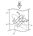
図1は、本実施形態に係る電流検出構造を示す図であり、(a)は平面図、(b)は斜視図である。 1A and 1B are diagrams showing a current detection structure according to the present embodiment, in which FIG. 1A is a plan view and FIG. 1B is a perspective view.
図1(a),(b)に示すように、電流検出構造1は、長手方向に沿って電流を流すバスバ2と、バスバ2を流れる電流により発生する磁界の強度を測定する磁気検出素子3と、を備えている。
As shown in FIGS. 1A and 1B, the current detection structure 1 includes a
バスバ2は、板状の導体であり、電流を流す電流路となるものである。磁気検出素子3としては、素子の高さ方向と垂直方向に検出軸Dを有し、高い感度を有するGMRセンサを用いる。
The
さて、本実施形態に係る電流検出構造1では、バスバ2に貫通孔からなるスロット4を形成し、磁気検出素子3を、スロット4の近傍に配置すると共に、その検出軸Dがバスバ2の長手方向に沿うように配置している。
Now, in the current detection structure 1 according to the present embodiment, the
図2に示すように、スロット4を形成することにより、スロット4を迂回するように電流が流れるようになる。その結果、バスバ2を流れる電流に幅方向(図示X方向)の成分が発生することとなり、この成分に起因してバスバ2の長手方向(図示Y方向)の成分を有する磁界が発生する。電流検出構造1では、スロット4を形成することによって発生したバスバ2の長手方向の磁界の強度Byを、磁気検出素子3により測定している。
As shown in FIG. 2, by forming the
スロット4で発生させるバスバ2の長手方向の磁界の強度Byは、周囲への影響を抑えるために出来るだけ小さくすることが望ましい。そのため、小さい磁界の強度Byを検出するために、スロット4のできるだけ近くに磁気検出素子3を配置することが望ましい。本実施形態では、平面視においてスロット4と重なる位置に磁気検出素子3を配置している。
The strength By of the magnetic field in the longitudinal direction of the
本実施形態では、磁気検出素子3としてGMRセンサを用いているため、小さい磁界も検出可能である。また、GMRセンサは素子の高さ方向と垂直方向に検出軸Dを有していることから、バスバ2と平行に(素子の高さ方向がバスバ2の厚さ方向となるように)磁気検出素子3を配置可能となり、電流検出構造1全体を薄型化することが可能になる。なお、図1では図示省略しているが、磁気検出素子3は、実際には、支持部材によりバスバ2やその周囲の部材等に支持されている。
In this embodiment, since a GMR sensor is used as the
スロット4を大きくし過ぎると、バスバ2の断面積が小さくなり抵抗が増加して発熱、損失が大きくなるので、スロット4はできるだけ小さくすることが望ましい。スロット4を小さくしても電流の幅方向の成分が発生しやすいように、スロット4は、その少なくとも一辺が、バスバ2の長手方向に対して交差するように形成されていることが望ましい。
If the
本実施形態では、2本の平行な辺の端部同士を円弧により接続した形状の略直線状のスロット4を、その中心軸がバスバ2の長手方向に対して傾斜するように形成している。バスバ2の長手方向に対するスロット4の中心軸の傾斜角度は、10°以上80°以下とすればよい。
In the present embodiment, the substantially
さらに、本実施形態では、同じ形状のスロット4を2つ離間して形成し、2つのスロット4に挟まれた隘路5を形成している。これにより、隘路5の幅等を調整することで、隘路5を流れる電流の大きさを調整し、バスバ2の長手方向に発生する磁界の強度、すなわち磁気検出素子3で検出する磁界の強度を容易に調整することが可能になる。電流検出構造1では、磁気検出素子3の感度等に応じて、磁気検出素子3で適切な強度の磁界を検出できるよう設計を行う必要があるが、隘路5を有する構成とすることで、このような設計が比較的容易となる。なお、隘路5は、少なくともその一部が、バスバ2の長手方向に対して交差する方向に形成されている必要がある。
Further, in this embodiment, two
ところで、例えば3相モータの各相に流れる電流を検出する場合では、通常、バスバ2を流れる電流全体により形成される磁界を計測するには、GMRセンサでは感度が高すぎ、他のバスバ2を流れる電流による磁界の影響も受けやすくなるために、そのままで測定を行うことは困難である。本実施形態では、スロット4の形状や隘路5の幅等を調整することにより、GMRセンサで測定するのに適した磁界の強度に調整し、かつ、バスバ2の長手方向の磁界の強度を測定するように構成することで周囲のバスバ2を流れる電流の影響を抑制しており、これにより、磁気検出素子3として高感度のGMRセンサを用いた場合であっても測定を可能としている。
By the way, when detecting the current flowing through each phase of a three-phase motor, for example, in order to measure the magnetic field formed by the entire current flowing through the
図3に示すように、電流検出構造1は、例えば、3相の各相の電流を測定する際に用いられる。3相の各相の電流路となる3つのバスバ2は、その幅方向に離間して整列配置されており、それぞれのバスバ2にスロット4が形成され、磁気検出素子3が配置されている。各バスバ2でスロット4を形成したことにより発生するバスバ2の長手方向の磁界は、互いに干渉することがなく、各磁気検出素子3が他のバスバ2の電流で発生した磁界の影響を受けることがない。
As shown in FIG. 3, the current detection structure 1 is used, for example, when measuring the current of each of three phases. The three
以上説明したように、本実施形態に係る電流検出構造1では、バスバ2にスロット4を形成し、磁気検出素子3を、スロット4の近傍に配置すると共に、その検出軸Dがバスバ2の長手方向に沿うように配置している。
As described above, in the current detection structure 1 according to the present embodiment, the
このように構成することで、検出対象以外のバスバ2を流れる電流により発生した磁界の影響を受けにくくなり、検出対象のバスバ2に流れる電流を精度よく検出することが可能になる。
With such a configuration, it is difficult to be affected by the magnetic field generated by the current flowing through the
また、スロット4の形状等を調整することで、磁気検出素子3の感度に応じて適切な強度の磁界を発生させることが可能であり、磁気検出素子3として高感度なGMRセンサを使用可能となる。GMRセンサは、素子の高さ方向と垂直方向に検出軸Dを有しているため、磁気検出素子3をバスバ2と平行に配置することが可能になり、電流検出構造1の薄型化に寄与する。
Further, by adjusting the shape of the
本発明は上記実施形態に限定されるものではなく、本発明の趣旨を逸脱しない範囲で種々の変更を加え得ることは勿論である。 The present invention is not limited to the above-described embodiment, and it is needless to say that various modifications can be made without departing from the spirit of the present invention.
例えば、上記実施形態では、略直線状のスロット4を2つ形成したが、これに限らず、図4(a)に示すように、スロット4をクランク状に形成してよいし、図4(b)に示すように、スロット4を1つのみとしてもよい。図示していないが、スロット4を3つ以上としても構わない。
For example, in the above-described embodiment, two substantially
さらに、図5(a)に示すように、スロット4を円形状としてもよいし、図5(b)に示すように、スロット4を矩形状としてもよい。このように、スロット4の形状や数は、特に限定されるものではなく、使用する磁気検出素子3の感度等に応じて、適宜選択可能である。
Furthermore, the
また、上記実施形態では、貫通孔からなるスロット4を形成した場合を説明したが、これに限らず、図6(a)に示すように、スロット4は、バスバ2の側方に開口する切欠き61からなってもよい。図6(a)では切欠き61を矩形状に形成しているが、図6(b)に示すように、対向する辺を傾斜させてもよく、切欠き61の形状は特に限定されない。
In the above embodiment, the case where the
スロット4を切欠き61とすることで、スロット4を形成する際に必要となる打ち抜き用の金型の構造をより簡易にすることができ、製造コストを低減できる。
By forming the
1 電流検出構造
2 バスバ
3 磁気検出素子
4 スロット
5 隘路
DESCRIPTION OF SYMBOLS 1
Claims (6)
前記バスバにスロットを形成し、
前記磁気検出素子を、前記スロットの近傍に配置すると共に、その検出軸が前記バスバの長手方向に沿うように配置した
ことを特徴とする電流検出構造。 A current detection structure comprising a bus bar for passing a current along the longitudinal direction, and a magnetic detection element for measuring the strength of a magnetic field generated by the current flowing through the bus bar,
Forming a slot in the bus bar;
The current detection structure, wherein the magnetic detection element is disposed in the vicinity of the slot, and the detection axis thereof is disposed along the longitudinal direction of the bus bar.
請求項1記載の電流検出構造。 The current detection structure according to claim 1, wherein the magnetic detection element is a GMR sensor.
請求項1または2記載の電流検出構造。 The current detection structure according to claim 1, wherein the slot is formed so that at least one side thereof intersects with a longitudinal direction of the bus bar.
請求項1〜3いずれかに記載の電流検出構造。 The current detection structure according to claim 1, wherein the slot is formed of a through hole formed in the bus bar.
前記隘路は、少なくともその一部が、前記バスバの長手方向に対して交差する方向に形成されている
請求項4記載の電流検出構造。 Forming two slots and forming a bottleneck sandwiched between the two slots;
The current detection structure according to claim 4, wherein at least a part of the bottleneck is formed in a direction intersecting with a longitudinal direction of the bus bar.
請求項1〜3いずれかに記載の電流検出構造。 The current detection structure according to claim 1, wherein the slot includes a notch that opens to a side of the bus bar.
Priority Applications (1)
| Application Number | Priority Date | Filing Date | Title |
|---|---|---|---|
| JP2014003473A JP2015132514A (en) | 2014-01-10 | 2014-01-10 | Electric current detection structure |
Applications Claiming Priority (1)
| Application Number | Priority Date | Filing Date | Title |
|---|---|---|---|
| JP2014003473A JP2015132514A (en) | 2014-01-10 | 2014-01-10 | Electric current detection structure |
Publications (1)
| Publication Number | Publication Date |
|---|---|
| JP2015132514A true JP2015132514A (en) | 2015-07-23 |
Family
ID=53899824
Family Applications (1)
| Application Number | Title | Priority Date | Filing Date |
|---|---|---|---|
| JP2014003473A Pending JP2015132514A (en) | 2014-01-10 | 2014-01-10 | Electric current detection structure |
Country Status (1)
| Country | Link |
|---|---|
| JP (1) | JP2015132514A (en) |
Cited By (2)
| Publication number | Priority date | Publication date | Assignee | Title |
|---|---|---|---|---|
| JP2016109663A (en) * | 2014-11-28 | 2016-06-20 | トヨタ自動車株式会社 | Current detector |
| CN112113785A (en) * | 2020-09-22 | 2020-12-22 | 北京小米移动软件有限公司 | Detection method and device, test equipment and storage medium |
Citations (2)
| Publication number | Priority date | Publication date | Assignee | Title |
|---|---|---|---|---|
| WO2011118184A1 (en) * | 2010-03-26 | 2011-09-29 | キヤノン電子株式会社 | Method for detecting magnetic field generated by a current to estimate the amount of current |
| US20120081110A1 (en) * | 2010-10-01 | 2012-04-05 | Robert Racz | Current sensor |
-
2014
- 2014-01-10 JP JP2014003473A patent/JP2015132514A/en active Pending
Patent Citations (2)
| Publication number | Priority date | Publication date | Assignee | Title |
|---|---|---|---|---|
| WO2011118184A1 (en) * | 2010-03-26 | 2011-09-29 | キヤノン電子株式会社 | Method for detecting magnetic field generated by a current to estimate the amount of current |
| US20120081110A1 (en) * | 2010-10-01 | 2012-04-05 | Robert Racz | Current sensor |
Cited By (3)
| Publication number | Priority date | Publication date | Assignee | Title |
|---|---|---|---|---|
| JP2016109663A (en) * | 2014-11-28 | 2016-06-20 | トヨタ自動車株式会社 | Current detector |
| CN112113785A (en) * | 2020-09-22 | 2020-12-22 | 北京小米移动软件有限公司 | Detection method and device, test equipment and storage medium |
| CN112113785B (en) * | 2020-09-22 | 2022-09-16 | 北京小米移动软件有限公司 | Detection method and device, test equipment and storage medium |
Similar Documents
| Publication | Publication Date | Title |
|---|---|---|
| JP6651956B2 (en) | Current sensor | |
| JP6690433B2 (en) | Current sensor | |
| JP5489145B1 (en) | Current sensor | |
| JP6711086B2 (en) | Current sensor | |
| JP6303527B2 (en) | Current sensor | |
| JP6403086B2 (en) | Current detection structure | |
| EP2770333B1 (en) | Current sensor | |
| JP2015137892A (en) | Current detection structure | |
| JP2016200436A (en) | Current sensor | |
| JP2016099292A (en) | Current detector and current detection method | |
| JP2008216230A (en) | Current sensor | |
| JP6115501B2 (en) | Current sensor | |
| JP2015148470A (en) | current detection structure | |
| JP2016200438A (en) | Current sensor | |
| JP2015132516A (en) | Electric current detection structure | |
| JP2021039030A (en) | Current sensor | |
| JP2015132514A (en) | Electric current detection structure | |
| JP2019100922A (en) | Current sensor | |
| JP3191252U (en) | Current sensor | |
| JP2014066623A (en) | Current sensor | |
| JP7192482B2 (en) | current sensor | |
| JP2013142569A (en) | Current sensor | |
| JP2015132515A (en) | Electric current detection structure | |
| JP2017133842A (en) | Current sensor and current detection device | |
| JP6413267B2 (en) | Current detection structure |
Legal Events
| Date | Code | Title | Description |
|---|---|---|---|
| A621 | Written request for application examination |
Free format text: JAPANESE INTERMEDIATE CODE: A621 Effective date: 20160318 |
|
| A977 | Report on retrieval |
Free format text: JAPANESE INTERMEDIATE CODE: A971007 Effective date: 20170118 |
|
| A131 | Notification of reasons for refusal |
Free format text: JAPANESE INTERMEDIATE CODE: A131 Effective date: 20170131 |
|
| A521 | Request for written amendment filed |
Free format text: JAPANESE INTERMEDIATE CODE: A523 Effective date: 20170324 |
|
| A02 | Decision of refusal |
Free format text: JAPANESE INTERMEDIATE CODE: A02 Effective date: 20170704 |