JP2015128027A - Organic el device and display device - Google Patents
Organic el device and display device Download PDFInfo
- Publication number
- JP2015128027A JP2015128027A JP2013273489A JP2013273489A JP2015128027A JP 2015128027 A JP2015128027 A JP 2015128027A JP 2013273489 A JP2013273489 A JP 2013273489A JP 2013273489 A JP2013273489 A JP 2013273489A JP 2015128027 A JP2015128027 A JP 2015128027A
- Authority
- JP
- Japan
- Prior art keywords
- organic
- layer
- light
- substrate
- color conversion
- Prior art date
- Legal status (The legal status is an assumption and is not a legal conclusion. Google has not performed a legal analysis and makes no representation as to the accuracy of the status listed.)
- Pending
Links
Images


Classifications
-
- H—ELECTRICITY
- H10—SEMICONDUCTOR DEVICES; ELECTRIC SOLID-STATE DEVICES NOT OTHERWISE PROVIDED FOR
- H10K—ORGANIC ELECTRIC SOLID-STATE DEVICES
- H10K59/00—Integrated devices, or assemblies of multiple devices, comprising at least one organic light-emitting element covered by group H10K50/00
- H10K59/30—Devices specially adapted for multicolour light emission
- H10K59/38—Devices specially adapted for multicolour light emission comprising colour filters or colour changing media [CCM]
-
- H—ELECTRICITY
- H10—SEMICONDUCTOR DEVICES; ELECTRIC SOLID-STATE DEVICES NOT OTHERWISE PROVIDED FOR
- H10K—ORGANIC ELECTRIC SOLID-STATE DEVICES
- H10K59/00—Integrated devices, or assemblies of multiple devices, comprising at least one organic light-emitting element covered by group H10K50/00
- H10K59/80—Constructional details
- H10K59/875—Arrangements for extracting light from the devices
- H10K59/879—Arrangements for extracting light from the devices comprising refractive means, e.g. lenses
Landscapes
- Devices For Indicating Variable Information By Combining Individual Elements (AREA)
- Electroluminescent Light Sources (AREA)
Abstract
Description
本発明は、有機EL装置、表示装置に関するものである。 The present invention relates to an organic EL device and a display device.
近年、液晶装置に代わり、有機エレクトロルミネッセンス(以下、有機ELと称する。)装置が注目されている。有機EL装置は、自発光であり、表示品質が高く、応答性能に優れ、薄型軽量化が可能、といった利点を有している。 In recent years, organic electroluminescence (hereinafter, referred to as organic EL) devices have attracted attention in place of liquid crystal devices. An organic EL device has the advantages that it is self-luminous, has high display quality, excellent response performance, and can be reduced in thickness and weight.
このような有機EL装置において、有機発光素子の出射面からの光取り出し効率を向上させる方法として、有機発光素子を有する第1基板と、カラーフィルターを有する第2基板と、の間にレンズ部材を接着する構成が提案されている(特許文献1)。 In such an organic EL device, as a method for improving the light extraction efficiency from the emission surface of the organic light emitting element, a lens member is provided between the first substrate having the organic light emitting element and the second substrate having the color filter. The structure which adhere | attaches is proposed (patent document 1).
しかしながら、特許文献1では、有機発光素子の上部電極およびカラーフィルターの両方にレンズ部材を接着させる必要があり、製造工程が複雑となってしまう。また、レンズ部材を透過した透過光は拡散するため、RGBの各サブ画素間において混色が生じてしまう。したがって、混色を生じさせることなく、光取り出し効率を向上させることは難しい。
However, in
本発明の一つの態様は、上記従来技術の問題点に鑑み成されたものであって、容易に製造でき、有機EL素子からの光の取り出し効率を向上させることができる有機EL装置、これを備えた表示装置を提供することを目的の一つとしている。 One aspect of the present invention is made in view of the above-described problems of the prior art, and can be easily manufactured, and an organic EL device capable of improving the light extraction efficiency from an organic EL element. An object is to provide a display device provided.
本発明の一つの態様の有機EL装置は、基板と、前記基板の一面に形成された有機EL素子と、を有する有機EL素子基板と、透明基板と、前記透明基板の一面に形成された色変換層と、を有する封止基板と、前記有機EL素子と前記透明基板との間に配置され、前記有機EL素子から射出された光を集光する集光部材と、前記有機EL素子基板と前記封止基板との間に充填され、前記集光部材よりも低屈折率を有する第1充填層と、を備えたことを特徴とする。 An organic EL device according to an aspect of the present invention includes a substrate, an organic EL element substrate having an organic EL element formed on one surface of the substrate, a transparent substrate, and a color formed on one surface of the transparent substrate. A conversion layer; a condensing member that is disposed between the organic EL element and the transparent substrate and collects light emitted from the organic EL element; and the organic EL element substrate. And a first filling layer filled between the sealing substrate and having a lower refractive index than that of the light collecting member.
本発明の一つの態様である有機EL装置において、前記有機EL素子と前記色変換層との間に前記集光部材が配置されている構成としてもよい。 In the organic EL device according to one aspect of the present invention, the light collecting member may be disposed between the organic EL element and the color conversion layer.
本発明の一つの態様である有機EL装置において、前記集光部材がレンズを含み、前記集光部材の焦点位置が、前記集光部材と前記色変換層との間に位置している構成としてもよい。 In the organic EL device according to one aspect of the present invention, the light collecting member includes a lens, and a focal position of the light collecting member is located between the light collecting member and the color conversion layer. Also good.
本発明の一つの態様である有機EL装置において、前記集光部材が、前記封止基板側の先端に集光面を有する光ファイバーからなる構成としてもよい。 In the organic EL device according to one aspect of the present invention, the condensing member may be composed of an optical fiber having a condensing surface at a tip on the sealing substrate side.
本発明の一つの態様である有機EL装置において、前記集光部材と前記色変換層との間に、前記集光部材を透過した光を通過させる開口を有した遮光部材が配置されている構成としてもよい。 In the organic EL device according to one aspect of the present invention, a light shielding member having an opening through which light transmitted through the light collecting member passes is disposed between the light collecting member and the color conversion layer. It is good.
本発明の一つの態様である有機EL装置において、前記集光部材の焦点位置が、前記開口内あるいは前記遮光部材と前記色変換層との間に位置する構成とされている構成としてもよい。 The organic EL device according to one aspect of the present invention may be configured such that a focal position of the light collecting member is located in the opening or between the light shielding member and the color conversion layer.
本発明の一つの態様である有機EL装置において、前記集光部材と前記色変換層との間に、特定波長の光を透過させるバンドパスフィルターが配置されている構成としてもよい。 The organic EL device according to one aspect of the present invention may be configured such that a band-pass filter that transmits light of a specific wavelength is disposed between the light collecting member and the color conversion layer.
本発明の一つの態様である有機EL装置において、前記遮光部材の前記色変換層側に第1反射層が設けられている構成としてもよい。 The organic EL device according to one aspect of the present invention may be configured such that a first reflective layer is provided on the color conversion layer side of the light shielding member.
本発明の一つの態様である有機EL装置において、前記透明基板と前記色変換層との間に色調整層が配置されている構成としてもよい。 In the organic EL device according to one aspect of the present invention, a color adjustment layer may be disposed between the transparent substrate and the color conversion layer.
本発明の一つの態様である有機EL装置において、前記色変換層と前記色調整層との間、あるいは前記色調整層と前記基板との間、あるいはその双方に、前記色変換層、前記色調整層、前記基板よりも低い屈折率を有する材料からなる低屈折率層が設けられている構成としてもよい。 In the organic EL device according to one aspect of the present invention, the color conversion layer and the color may be provided between the color conversion layer and the color adjustment layer, or between the color adjustment layer and the substrate, or both. The adjustment layer and a low refractive index layer made of a material having a lower refractive index than that of the substrate may be provided.
本発明の一つの態様である有機EL装置において、前記色調整層は、前記色変換層よりも低屈折率とされている構成としてもよい。 In the organic EL device according to one aspect of the present invention, the color adjustment layer may have a lower refractive index than the color conversion layer.
本発明の一つの態様である有機EL装置において、前記有機EL素子を区画する第1バンクを備え、前記第1バンクは、前記基板に対向する第1端面と、前記第1端面に対向し当該第1端面の面積よりも小さい面積を有する第2端面と、側面と、により構成され、前記側面に、前記有機EL素子から放出された光を前記集光部材側へと反射させる第2反射層が設けられている構成としてもよい。 In the organic EL device according to one aspect of the present invention, the organic EL device includes a first bank that partitions the organic EL element, the first bank facing the first end surface and the first end surface facing the substrate. A second reflection layer that includes a second end surface having an area smaller than the area of the first end surface and a side surface, and reflects the light emitted from the organic EL element toward the light collecting member side on the side surface. It is good also as a structure provided.
本発明の一つの態様である有機EL装置において、前記有機EL素子と前記集光部材との間に、前記有機EL素子を封止する封止層が設けられている構成としてもよい。 In the organic EL device according to one aspect of the present invention, a sealing layer for sealing the organic EL element may be provided between the organic EL element and the light collecting member.
本発明の一つの態様である有機EL装置において、前記透明基板上を所定領域ごとに区画する第2バンクを備え、前記第2バンクは、前記透明基板の前記一面に対向する第1端面と、前記第1端面に対向し当該第1端面の面積よりも小さい面積を有する第2端面と、側面と、により構成されているとしてもよい。 In the organic EL device according to one aspect of the present invention, the organic EL device includes a second bank that partitions the transparent substrate into predetermined regions, and the second bank has a first end surface facing the one surface of the transparent substrate; The second end surface that faces the first end surface and has an area smaller than the area of the first end surface, and a side surface may be configured.
本発明の一つの態様である有機EL装置において、前記集光部材と前記色変換層との間に、前記集光部材を透過した光を通過させる開口を有した遮光部材と、前記遮光部材の前記色変換層側に第1反射層とが配置されており、前記透明基板の前記一面に対向する第1端面と、前記第1端面に対向し当該第1端面の面積よりも小さい面積を有する第2端面と、側面と、により構成されている前記第2バンクの前記側面に、前記色変換層及び前記色調整層から射出された光を前記第1反射層側へと反射させる第3反射層が設けられている構成としてもよい。 In the organic EL device according to one aspect of the present invention, a light shielding member having an opening through which light transmitted through the light collecting member passes between the light collecting member and the color conversion layer; and A first reflective layer is disposed on the color conversion layer side, and has a first end surface facing the one surface of the transparent substrate and an area facing the first end surface and smaller than the area of the first end surface. Third reflection for reflecting light emitted from the color conversion layer and the color adjustment layer toward the first reflective layer on the side surface of the second bank configured by a second end surface and a side surface. It is good also as a structure in which the layer is provided.
本発明の一つの態様である有機EL装置において、前記透明基板上を所定領域ごとに区画する第2バンクを備え、前記第2バンクは、前記透明基板の前記一面に対向する第1端面と、前記第1端面に対向し当該第1端面の面積よりも大きい面積を有する第2端面と、側面と、により構成され、前記側面に、前記色変換層及び前記色調整層から射出された光を前記透明基板側へと反射させる第3反射層が設けられている構成としてもよい。 In the organic EL device according to one aspect of the present invention, the organic EL device includes a second bank that partitions the transparent substrate into predetermined regions, and the second bank has a first end surface facing the one surface of the transparent substrate; The second end surface facing the first end surface and having an area larger than the area of the first end surface, and a side surface, and the light emitted from the color conversion layer and the color adjustment layer on the side surface It is good also as a structure provided with the 3rd reflection layer reflected in the said transparent substrate side.
本発明の一つの態様である有機EL装置において、前記第2バンクが可視光を透過しないブラックマトリクスから構成されていてもよい。 In the organic EL device according to one aspect of the present invention, the second bank may be composed of a black matrix that does not transmit visible light.
本発明の一つの態様である有機EL装置において、前記色変換層と前記色調整層との間に前記集光部材が配置されるとともに、前記集光部材と前記色調整層との間に第2充填層が配置されており、前記透明基板の前記一面とは反対側の視認側の面に光散乱部材が設けられている構成としてもよい。 In the organic EL device according to one aspect of the present invention, the light condensing member is disposed between the color conversion layer and the color adjustment layer, and a second portion is disposed between the light condensing member and the color adjustment layer. It is good also as a structure by which 2 filling layers are arrange | positioned and the light-scattering member is provided in the surface at the side of visual recognition opposite to the said one surface of the said transparent substrate.
本発明の表示装置は、上記の有機EL素子を備えたことを特徴とする。 A display device according to the present invention includes the organic EL element described above.
本発明によれば、有機EL素子からの光の取り出し効率を向上させることができるとともに容易に製造できる有機EL装置、表示装置を提供することができる。 According to the present invention, it is possible to provide an organic EL device and a display device that can improve the light extraction efficiency from the organic EL element and can be easily manufactured.
以下、本発明の実施形態につき、図面を参照して説明する。なお、以下の説明に用いる各図面では、各部材を認識可能な大きさとするため、各部材の縮尺を適宜変更している。 Embodiments of the present invention will be described below with reference to the drawings. In each drawing used for the following description, the scale of each member is appropriately changed to make each member a recognizable size.
[第1実施形態]
図1(A)は、本発明の第1実施形態である有機EL装置の概略構成を示す断面図である。図1(B)は、有機発光素子の概略構成を示す図である。
図1(A)に示すように、本実施形態における有機EL装置100は、有機EL素子基板(以下、単に「素子基板20」と称する。)と、波長変換基板(封止基板)30と、素子基板20及び波長変換基板30との間に設けられた充填層(第1充填層)16と、を備えた、アクティブ駆動方式で駆動されるトップエミッションタイプの有機EL装置である。
[First Embodiment]
FIG. 1A is a cross-sectional view showing a schematic configuration of an organic EL device according to the first embodiment of the present invention. FIG. 1B is a diagram illustrating a schematic configuration of an organic light emitting element.
As shown in FIG. 1A, an
素子基板20は、第1基板、TFT(薄膜トランジスタ)回路2、有機発光素子(有機EL素子)10を主として構成されており、TFT回路2を備えた第1基板1上に複数の有機発光素子10が設けられている。
The
波長変換基板(封止基板)30は、透明基板9、カラーフィルター層(色調整層)14及び色変換層15を主として構成されており、透明基板9の一面9a側に、R,G,Bの各サブ画素Sに対応したカラーフィルター層(色調整層)14及び色変換層15が設けられている。
The wavelength conversion substrate (sealing substrate) 30 mainly includes a
本実施形態の有機EL装置100は、光源である有機発光素子(有機EL素子)10から発光された光が色変換層15及びカラーフィルター層14へと入射することで、赤色、緑色、青色の三色の光として波長変換基板30の外側(観測者側)へと射出されるようになっている。
In the
図1(B)に示すように、有機発光素子10は、有機EL層13が第1電極11と第2電極12とにより挟持されて構成されている。図1(A)に示すように、第1電極11は、層間絶縁膜3及び平坦化膜4を貫通して設けられたコンタクトホール2bにより、TFT回路2の1つに接続されている。第2電極12は、層間絶縁膜3、平坦化膜4を貫通して設けられた不図示の配線によりTFT回路2の1つに接続されている。
As shown in FIG. 1B, the organic
図2は、第1実施形態における有機EL装置の上面図である。
図2に示すように、本実施形態の有機EL装置100は、複数の画素22を有している。各画素22は、赤色光(R)、緑色光(G)、青色光(B)のそれぞれに対応する3つのサブ画素S(赤色画素部S(R)、緑色画素部S(G)、青色画素部S(B))から構成されている。
FIG. 2 is a top view of the organic EL device according to the first embodiment.
As shown in FIG. 2, the
赤色画素部S(R)、緑色画素部S(G)、青色画素部S(B)は、y軸に沿ってストライプ状に延長され、x軸に沿って赤色画素部S(R)、緑色画素部S(G)、青色画素部S(B)が順に配置された、2次元的なストライプ配列とされている。 The red pixel portion S (R), the green pixel portion S (G), and the blue pixel portion S (B) extend in a stripe shape along the y axis, and the red pixel portion S (R), green color along the x axis. The pixel portion S (G) and the blue pixel portion S (B) are arranged in this order to form a two-dimensional stripe arrangement.
なお、図2に示す例ではRGBの各サブ画素(赤色画素部S(R)、緑色画素部S(G)、青色画素部S(B))がストライプ配列された例を示しているが、本発明はこれに限定されず、RGBの各サブ画素(赤色画素部S(R)、緑色画素部S(G)、青色画素部S(B))の配列はモザイク配列、デルタ配列など、従来公知のRGB画素配列とすることもできる。 The example shown in FIG. 2 shows an example in which each RGB sub-pixel (red pixel portion S (R), green pixel portion S (G), blue pixel portion S (B)) is arranged in stripes. The present invention is not limited to this, and the arrangement of each of the RGB sub-pixels (red pixel portion S (R), green pixel portion S (G), blue pixel portion S (B)) is a conventional arrangement such as a mosaic arrangement or a delta arrangement. A known RGB pixel array may be used.
<素子基板>
素子基板20は、図1(A)に示すように、アクティブマトリクス基板25と、アクティブマトリクス基板25上に設けられた複数の有機発光素子10、第1バンク8、封止層5及び複数の集光部材7とを有して構成されている。アクティブマトリクス基板25は、第1基板1、第1基板1上に形成されたTFT回路2、層間絶縁膜3及び平坦化膜4を有する。
<Element substrate>
As shown in FIG. 1A, the
第1基板1上には、TFT回路2及び各種配線(図示略)が形成され、さらに、第1基板1の上面およびTFT回路2を覆うように層間絶縁膜3と平坦化膜4が順次積層形成されている。
A
第1基板1としては、例えば、ガラス、石英等からなる無機材料基板、ポリエチレンテレフタレート、ポリカルバゾール、ポリイミド等からなるプラスティック基板、アルミナ等からなるセラミックス基板等の絶縁性基板、アルミニウム(Al)、鉄(Fe)等からなる金属基板、前記基板上に酸化シリコン(SiO2)などの有機絶縁材料等からなる絶縁物を表面にコーティングした基板、又は、Al等からなる金属基板の表面を陽極酸化等の方法で絶縁化処理を施した基板等が挙げられるが、本発明はこれらに限定されるものではない。
As the
TFT回路2は、有機発光素子10を形成する前に、予め第1基板1上に形成され、スイッチング用及び駆動用として機能する。TFT回路2としては、従来公知のTFT回路2を用いることができる。また、本発明においては、スイッチング用及び駆動用素子としてTFTの代わりに金属−絶縁体−金属(MIM)ダイオードを用いることもできる。
The
TFT回路2は、公知の材料、構造及び形成方法を用いて形成することができる。TFT回路2の活性層の材料としては、例えば、非晶質シリコン(アモルファスシリコン)、多結晶シリコン(ポリシリコン)、微結晶シリコン、セレン化カドミウム等の無機半導体材料、酸化亜鉛、酸化インジウム−酸化ガリウム−酸化亜鉛等の酸化物半導体材料又は、ポリチオフェン誘導体、チオフエンオリゴマー、ポリ(p−フェリレンビニレン)誘導体、ナフタセン、ペンタセン等の有機半導体材料が挙げられる。また、TFT回路2の構造としては、例えば、スタガ型、逆スタガ型、トップゲート型、コプレーナ型が挙げられる。
The
本発明で用いられるTFT回路2のゲート絶縁膜は、公知の材料を用いて形成することができる。例えば、プラズマ誘起化学気相成長(PECVD)法、減圧化学気相成長(LPCVD)法等により形成されたSiO2又はポリシリコン膜を熱酸化して得られるSiO2等が挙げられる。また、本発明で用いられるTFT回路2の信号電極線、走査電極線、共通電極線、第1駆動電極及び第2駆動電極は、公知の材料を用いて形成することができ、例えば、タンタル(Ta)、アルミニウム(Al)、銅(Cu)等が挙げられる。
The gate insulating film of the
層間絶縁膜3は、公知の材料を用いて形成することができ、例えば、酸化シリコン(SiO2)、窒化シリコン(SiN、又は、Si2N4)、酸化タンタル(TaO、又は、Ta2O5)等の無機材料、又は、アクリル樹脂、レジスト材料等の有機材料等が挙げられる。
The
層間絶縁膜3の形成方法としては、化学気相成長(CVD)法、真空蒸着法等のドライプロセス、スピンコート法等のウエットプロセスが挙げられる。また、必要に応じてフォトリソグラフィー法等によりパターニングすることもできる。
Examples of the method for forming the
平坦化膜4は、TFT回路2の表面の凸凹により有機発光素子10の欠陥(例えば、画素電極の欠損、有機EL層の欠損、対向電極の断線、画素電極と対向電極の短絡、耐圧の低下等)等が発生することを防止するために設けられるものである。なお、平坦化膜4は省略することも可能である。
The
平坦化膜4は、公知の材料を用いて形成することができ、例えば、酸化シリコン、窒化シリコン、酸化タンタル等の無機材料、ポリイミド、アクリル樹脂、レジスト材料等の有機材料等が挙げられる。平坦化膜4の形成方法としては、CVD法、真空蒸着法等のドライプロセス、スピンコート法等のウエットプロセスが挙げられるが、本発明はこれらの材料及び形成方法に限定されるものではない。また、平坦化膜4は、単層構造でも多層構造でもよい。
The
第1バンク8は、有機発光素子10の周囲を取り囲み、各サブ画素Sを区画するようにして形成されている。第1バンク8は、第1基板1の一面1a上の少なくとも各サブ画素S間に形成され、第1電極11と第2電極12との間でリークを起こすことを防止するものである。
The
具体的に、第1バンク8は、第1基板1に対向する第1端面8aと、第1端面8aに対向して第1端面8aの面積よりも小さい面積を有する第2端面8bと、側面8cと、を有した順テーパー形状となっている。ここで、「順テーパー形状」とは、第1基板1から離れる方向に断面形状が細くなるテーパー形状のことをいう。
Specifically, the
本実施形態における第1バンク8は、有機発光素子10からの光取り出し効率を考慮した白色のホワイトバンクからなる。これにより輝度が向上する。
第1バンク8は、絶縁材料を用いて、電子線(EB)蒸着法、スパッタリング法、イオンプレーティング法、抵抗加熱蒸着法等の公知の方法により形成することができる。また、第1バンク8は、公知のドライ法またはウェット法のフォトリソグラフィー法によりパターン化することができる。なお、第1バンク8の形成方法は、これらの形成方法に限定されるものではない。また、第1バンク8を構成する材料としては、特に限定されるものではないが、公知の材料が用いられる。例えば、平坦化膜4と同様の材料を用いることも可能である。
The
The
第1バンク8は、第1電極11と第2電極12との絶縁性を十分に確保することのできる膜厚を有する。第1バンク8の膜厚としては、例えば、100nm〜2000nmであることが好ましい。第1バンク8の膜厚が100nm未満であると、絶縁性が十分ではなく、第1電極11と第2電極12との間でリークが起こり、消費電力の上昇、非発光の原因となる。一方、第1バンク8の膜厚が2000nmを超えると、成膜プロセスに時間がかかるため生産性の悪化が懸念される。
The
(有機EL素子)
有機発光素子10は、第1電極11、有機EL層13、第2電極12を有する。
第1電極11及び第2電極12は、有機発光素子10の陽極または陰極として対で機能する。図1(A)、(B)及び以下の説明においては、第1電極11が陽極、第2電極12が陰極の場合を例に説明する。
(Organic EL device)
The organic
The
第1電極11及び第2電極12は、従来の電極材料を用いて形成することができる。
第1電極11は、例えば、有機EL層13に電子を効率良く注入するために、Ca/AlやCe/Al、Cs/Al、Ba/Alなどの仕事関数の低い金属と安定な金属とを積層して形成するのが好ましい。また、第1電極11は、Ca:Al合金やMg:Ag合金、Li:Al合金などの仕事関数の低い金属を含有する合金で形成してもよいし、LiF/AlやLiF/Ca/Al、BaF2/Ba/Al、LiF/Al/Agなどの薄膜の絶縁層と金属電極とを組み合わせて形成してもよい。
The
For example, in order to efficiently inject electrons into the
第2電極12は、ITOやIDIXO、IZO、GZO、SnO2などを用いて透明電極を形成することができる。第1電極11と第2電極12により微小共振器構造を構成する場合、第2電極12として半透明電極を用いることが好ましい。
As the
第2電極12としては、金属の半透明電極と透明電極材料を組み合わせたものを用いることができる。特に、半透明電極の材料としては、反射率と透過率の観点から、銀が好ましい。半透明電極の膜厚は、5〜30nmが好ましい。半透明電極の膜厚が5nm未満の場合には、光の反射が十分行えず、干渉の効果を十分得ることができない。また、半透明電極の膜厚が30nmを超える場合には、光の透過率が急激に低下することから、有機発光素子10の輝度および発光効率が低下するおそれがある。
As the
有機EL層13は、第1電極11と第2電極12との間に配置され、電圧が印加されることによって発光する。有機EL層13は、例えば、図1(B)に示すように、第1電極11側から順に、正孔注入層34、正孔輸送層35、電子ブロッキング層36、発光層37、電子輸送層38、電子注入層39が設けられている(正孔注入層/正孔輸送層/電子ブロッキング層/発光層/電子輸送層/電子注入層)。本実施形態の発光層37は、青色〜青緑色光を発光する単層構造とされている。
The
第1電極11と第2電極12により微小共振器構造が構成されると、第1電極11と第2電極12との干渉効果により、有機EL層13の発光を正面方向(光取り出し方向)に集光することができる。その際、有機EL層13の発光に指向性を持たせることができるため、周囲に逃げる発光損失を低減することができ、その発光効率を高めることができる。これにより、有機EL層13で生じる発光エネルギーをより効率良く、色変換層15側へ出射させることができ、ひいては、有機発光素子10の正面輝度を高めることができる。
When the microresonator structure is configured by the
また、第1電極11と第2電極12により構成される微小共振器構造によれば、有機EL層13の発光スペクトルを調整することも可能となり、所望の発光ピーク波長および半値幅に調整することができる。これにより、有機EL層13の発光スペクトルを、色変換層15中の有機蛍光色素を効果的に励起することが可能なスペクトルに制御することができる。
In addition, according to the microresonator structure constituted by the
第1電極11及び第2電極12の形成には、蒸着法やEB法、MBE法、スパッタ法等のドライプロセスを用いることできるし、また、スピンコート法や印刷法、インクジェット法等のウエットプロセスを用いることもできる。
The
正孔注入層34は、第1電極11から効率良く正孔を受け取り、正孔輸送層35へ効率良く受け渡すために設けられている。正孔注入層34に用いられる材料のHOMOレベルは、正孔輸送層35に用いられるHOMOレベルよりも低く、第1電極11の仕事関数よりも高いのが好ましい。正孔注入層34は、単層でも多層であってもよい。
The
接着用の樹脂には、例えば、ポリカーボネートやポリエステル等を用いることができる。溶剤は、材料を溶解、または分散できるものであればく、例えば、純水、メタノール、エタノール、THF、クロロホルム、キシレン、トリメチルベンゼン等を溶剤に用いることができる。 For example, polycarbonate or polyester can be used as the adhesive resin. Any solvent can be used as long as it can dissolve or disperse the material. For example, pure water, methanol, ethanol, THF, chloroform, xylene, trimethylbenzene, or the like can be used as the solvent.
正孔注入層34の材料には、有機EL素子や有機光導電体に対して一般に用いられているものを用いることができる。例えば、無機p型半導体材料や、ポルフィリン化合物、N,N'−ビス−(3‐メチルフェニル)−N,N'−ビス−(フェニル)−ベンジジン(TPD)、N,N'−ジ(ナフタレン‐1‐イル)−N,N'−ジフェニル−ベンジジン(NPD)等の芳香族第三級アミン化合物、ヒドラゾン化合物、キナクリドン化合物、スチリルアミン化合物等の低分子材料、ポリアニリン(PANI)、3,4−ポリエチレンジオキシチオフェン/ポリスチレンサルフォネイト(PEDT/PSS)、ポリ[トリフェニルアミン誘導体](Poly−TPD)、ポリビニルカルバゾール(PVCz)等の高分子材料、ポリ(p−フェニレンビニレン)前駆体(Pre−PPV)、ポリ(p−ナフタレンビニレン)前駆体(Pre−PNV)等の高分子材料前駆体などを用いることができる。
As the material of the
正孔輸送層35は、正孔注入層34から効率良く正孔を受け取り、発光層37へ効率良く受け渡すために設けられている。正孔輸送層35に用いられる材料のHOMOレベルは、正孔注入層34のHOMOレベルよりも高く、発光層37のHOMOレベルよりも低いのが好ましい。正孔をより効率よく発光層37に注入、輸送でき、発光に要する電圧の低減効果や発光効率の向上効果を得ることができるからである。
The
また、発光層37からの電子の漏れが抑制できるように、正孔輸送層35のLUMOレベルは発光層37のLUMOレベルより低くするのが好ましい。そうすれば、発光層37での発光効率を高めることができる。また、正孔輸送層35のバンドギャップは発光層37のバンドギャップより大きくするのが好ましい。そうすれば、発光層37中に励起子を効果的に閉じ込めることができる。
In addition, the LUMO level of the
正孔輸送層35は、単層でも多層でもよく、ドライプロセスやウエットプロセスを用い、正孔注入層34と同じようにして形成することができる。
The
電子ブロッキング層36は、正孔注入層34と同種の材料を用いて形成することができる。但し、その材料のLUMOレベルの絶対値は、電子ブロッキング層36と接する発光層37が含む正孔注入層34の材料のLUMOレベルの絶対値より小さいのが好ましい。電子をより効果的に発光層37中に閉じ込めることができるからである。
電子ブロッキング層36もまた、単層でも多層であってもよく、ドライプロセスやウエットプロセスを用い、正孔注入層34と同じようにして形成することができる。
The
The
発光層37は、以下に例示する有機発光材料のみから構成されていてもよく、発光性のドーパントとホスト材料の組み合わせから構成されていてもよく、任意に正孔輸送材料、電子輸送材料、添加剤(ドナー、アクセプター等)等を含んでいてもよい。また、これらの各材料が高分子材料(接着用樹脂)または無機材料中に分散された構成であってもよい。発光効率および耐久性の観点からは、発光層37の材質は、ホスト材料中に発光性のドーパントが分散されたものが好ましい。
The
有機発光材料としては、有機EL素子向けの公知の発光材料を用いることができる。
このような発光材料は、低分子発光材料、高分子発光材料等に分類され、これらの具体
的な化合物を以下に例示するが、本実施形態はこれらの材料に限定されるものではない。また、有機発光材料は、蛍光材料、燐光材料等に分類されるものでもよく、低消費電力化の観点から、発光効率の高い燐光材料を用いることが好ましい。
As the organic light emitting material, a known light emitting material for an organic EL element can be used.
Such light-emitting materials are classified into low-molecular light-emitting materials, polymer light-emitting materials, and the like. Specific examples of these compounds are given below, but the present embodiment is not limited to these materials. The organic light emitting material may be classified into a fluorescent material, a phosphorescent material, and the like. From the viewpoint of reducing power consumption, it is preferable to use a phosphorescent material with high emission efficiency.
発光層37に用いられる低分子発光材料(ホスト材料を含む)としては、4,4
’−ビス(2,2’−ジフェニルビニル)−ビフェニル(DPVBi)等の芳香族ジメチリデン化合物;5−メチル−2−[2−[4−(5−メチル−2−ベンゾオキサゾリル)フェニル]ビニル]ベンゾオキサゾール等のオキサジアゾール化合物;3−(4−ビフェニル)−4−フェニル−5−t−ブチルフェニル−1,2,4−トリアゾール(TAZ)等のトリアゾール誘導体;1,4−ビス(2−メチルスチリル)ベンゼン等のスチリルベンゼン化合物;チオピラジンジオキシド誘導体、ベンゾキノン誘導体、ナフトキノン誘導体、アントラキノン誘導体、ジフェノキノン誘導体、フルオレノン誘導体等の蛍光性有機材料;アゾメチン亜鉛錯体、(8−ヒドロキシキノリナト)アルミニウム錯体(Alq3)等の蛍光発光有機金属錯体;BeBq(ビス(ベンゾキノリノラト)ベリリウム錯体);4,4’−ビス−(2,2−ジ−p−トリル−ビニル)−ビフェニル(DTVBi);トリス(1,3−ジフェニル−1,3−プロパンジオノ)(モノフェナントロリン)Eu(III)(Eu(DBM)3(Phen));ジフェニルエチレン誘導体;トリス[4−(9−フェニルフルオレン−9−イル)フェニル]アミン(TFTPA)等のトリフェニルアミン誘導体;ジアミノカルバゾール誘導体;ビススチリル誘導体;芳香族ジアミン誘導体;キナクリドン系化合物;ペリレン系化合物;クマリン系化合物;ジスチリルアリーレン誘導体(DPVBi);オリゴチオフェン誘導体(BMA−3T);4,4’−ジ(トリフェニルシリル)−ビフェニル(BSB)、ジフェニル−ジ(o−トリル)シラン(UGH1)、1,4−ビストリフェニルシリルベンゼン(UGH2)、1,3−ビス(トリフェニルシリル)ベンゼン(UGH3)、トリフェニル−(4−(9−フェニル−9H−フルオレン−9−イル)フェニル)シラン(TPSi−F)等のシラン誘導体;9,9−ジ(4−ジカルバゾール−ベンジル)フルオレン(CPF)、3,6−ビス(トリフェニルシリル)カルバゾール(mCP)、4,4’−ビス(カルバゾール−9−イル)ビフェニル(CBP)、4,4’−ビス(カルバゾール−9−イル)−2,2’−ジメチルビフェニル(CDBP)、N,N−ジカルバゾリル−3,5−ベンゼン(m−CP)、3−(ジフェニルホスホリル)−9−フェニル−9H−カルバゾール(PPO1)、3,6−ジ(9−カルバゾリル)−9−(2−エチルヘキシル)カルバゾール(TCz1)、9,9’−(5−(トリフェニルシリル)−1,3−フェニレン)ビス(9H−カルバゾール)(SimCP)、ビス(3,5−ジ(9H−カルバゾール−9−イル)フェニル)ジフェニルシラン(SimCP2)、3−(ジフェニルホスホリル)−9−(4−ジフェニルホスホリル)フェニル)−9H−カルバゾール(PPO21)、2,2−ビス(4−カルバゾリルフェニル)−1,1−ビフェニル(4CzPBP)、3,6−ビス(ジフェニルホスホリル)−9−フェニル−9H−カルバゾール(PPO2)、9−(4−tert−ブチルフェニル)−3,6−ビス(トリフェニルシリル)−9H−カルバゾール(CzSi)、3,6−ビス[(3,5−ジフェニル)フェニル]−9−フェニル−カルバゾール(CzTP)、9−(4−tert−ブチルフェニル)−3,6−ジトリチル−9H−カルバゾール(CzC)、9−(4−tert−ブチルフェニル)−3,6−ビス(9−(4−メトキシフェニル)−9H−フルオレン−9−イル)−9H−カルバゾール(DFC)、2,2’−ビス(4−カルバゾール−9−イル)フェニル)−ビフェニル(BCBP)、9,9’−((2,6−ジフェニルベンゾ[1,2−b:4,5−b’]ジフラン−3,7−ジイル)ビス(4,1−フェニレン))ビス(9H−カルバゾール)(CZBDF)等のカルバゾール誘導体;4−(ジフェニルフォスフォイル)−N,N−ジフェニルアニリン(HM−A1)等のアニリン誘導体;1,3−ビス(9−フェニル−9H−フルオレン−9−イル)ベンゼン(mDPFB)、1,4−ビス(9−フェニル−9H−フルオレン−9−イル)ベンゼン(pDPFB)、2,7−ビス(カルバゾール−9−イル)−9,9−ジメチルフルオレン(DMFL−CBP)、2−[9,9−ジ(4−メチルフェニル)−フルオレン−2−イル]−9,9−ジ(4−メチルフェニル)フルオレン(BDAF)、2−(9,9−スピロビフルオレン−2−イル)−9,9−スピロビフルオレン(BSBF)、9,9−ビス[4−(ピレニル)フェニル]−9H−フルオレン(BPPF)、2,2’−ジピレニル−9,9−スピロビフルオレン(Spiro−Pye)、2,7−ジピレニル−9,9−スピロビフルオレン(2,2’−Spiro−Pye)、2,7−ビス[9,9−ジ(4−メチルフェニル)−フルオレン−2−イル]−9,9−ジ(4−メチルフェニル)フルオレン(TDAF)、2,7−ビス(9,9−スピロビフルオレン−2−イル)−9,9−スピロビフルオレン(TSBF)、9,9−スピロビフルオレン−2−イル−ジフェニル−フォスフィンオキサイド(SPPO1)等のフルオレン誘導体;1,3−ジ(ピレン−1−イル)ベンゼン(m−Bpye)等のピレン誘導体;プロパン−2,2’−ジイルビス(4,1−フェニレン)ジベンゾエート(MMA1)等のベンゾエート誘導体;4,4’−ビス(ジフェニルフォスフィンオキサイド)ビフェニル(PO1)、2,8−ビス(ジフェニルフォスフォリル)ジベンゾ[b,d]チオフェン(PPT)等のフォスフィンオキサイド誘導体;4,4”−ジ(トリフェニルシリル)−p−ターフェニル(BST)等のターフェニル誘導体;2,4−ビス(フェノキシ)−6−(3−メチルジフェニルアミノ)−1,3,5−トリアジン(BPMT)等トリアジン誘導体等が挙げられる。
As the low-molecular light-emitting materials (including host materials) used for the light-emitting
Aromatic dimethylidene compounds such as' -bis (2,2'-diphenylvinyl) -biphenyl (DPVBi); 5-methyl-2- [2- [4- (5-methyl-2-benzoxazolyl) phenyl] Oxadiazole compounds such as vinyl] benzoxazole; triazole derivatives such as 3- (4-biphenyl) -4-phenyl-5-t-butylphenyl-1,2,4-triazole (TAZ); 1,4-bis Styrylbenzene compounds such as (2-methylstyryl) benzene; fluorescent organic materials such as thiopyrazine dioxide derivatives, benzoquinone derivatives, naphthoquinone derivatives, anthraquinone derivatives, diphenoquinone derivatives, fluorenone derivatives; azomethine zinc complexes, (8-hydroxyquinolinato ) Fluorescent organic metal complexes such as aluminum complexes (Alq3); eBq (bis (benzoquinolinolato) beryllium complex); 4,4′-bis- (2,2-di-p-tolyl-vinyl) -biphenyl (DTVBi); tris (1,3-diphenyl-1,3 -Propanediono) (monophenanthroline) Eu (III) (Eu (DBM) 3 (Phen)); diphenylethylene derivatives; tris [4- (9-phenylfluoren-9-yl) phenyl] amine (TTPPA) Diaminocarbazole derivatives; Bisstyryl derivatives; Aromatic diamine derivatives; Quinacridone compounds; Perylene compounds; Coumarin compounds; Distyrylarylene derivatives (DPVBi); Oligothiophene derivatives (BMA-3T); Di (triphenylsilyl) -biphenyl (BSB), diphenyl- (O-Tolyl) silane (UGH1), 1,4-bistriphenylsilylbenzene (UGH2), 1,3-bis (triphenylsilyl) benzene (UGH3), triphenyl- (4- (9-phenyl-9H- Silane derivatives such as fluoren-9-yl) phenyl) silane (TPSi-F); 9,9-di (4-dicarbazole-benzyl) fluorene (CPF), 3,6-bis (triphenylsilyl) carbazole (mCP) ), 4,4′-bis (carbazol-9-yl) biphenyl (CBP), 4,4′-bis (carbazol-9-yl) -2,2′-dimethylbiphenyl (CDBP), N, N-dicarbazolyl -3,5-benzene (m-CP), 3- (diphenylphosphoryl) -9-phenyl-9H-carbazole (PPO1), 3,6-di (9 Carbazolyl) -9- (2-ethylhexyl) carbazole (TCz1), 9,9 ′-(5- (triphenylsilyl) -1,3-phenylene) bis (9H-carbazole) (SimCP), bis (3,5 -Di (9H-carbazol-9-yl) phenyl) diphenylsilane (SimCP2), 3- (diphenylphosphoryl) -9- (4-diphenylphosphoryl) phenyl) -9H-carbazole (PPO21), 2,2-bis ( 4-carbazolylphenyl) -1,1-biphenyl (4CzPBP), 3,6-bis (diphenylphosphoryl) -9-phenyl-9H-carbazole (PPO2), 9- (4-tert-butylphenyl) -3 , 6-Bis (triphenylsilyl) -9H-carbazole (CzSi), 3,6-bis [(3,5-diph Nyl) phenyl] -9-phenyl-carbazole (CzTP), 9- (4-tert-butylphenyl) -3,6-ditrityl-9H-carbazole (CzC), 9- (4-tert-butylphenyl) -3 , 6-Bis (9- (4-methoxyphenyl) -9H-fluoren-9-yl) -9H-carbazole (DFC), 2,2′-bis (4-carbazol-9-yl) phenyl) -biphenyl ( BCBP), 9,9 ′-((2,6-diphenylbenzo [1,2-b: 4,5-b ′] difuran-3,7-diyl) bis (4,1-phenylene)) bis (9H Carbazole derivatives such as carbazole) (CZBDF); aniline derivatives such as 4- (diphenylphosphoyl) -N, N-diphenylaniline (HM-A1); 1,3-bis (9-pheny -9H-fluoren-9-yl) benzene (mDPFB), 1,4-bis (9-phenyl-9H-fluoren-9-yl) benzene (pDPFB), 2,7-bis (carbazol-9-yl) -9,9-dimethylfluorene (DMFL-CBP), 2- [9,9-di (4-methylphenyl) -fluoren-2-yl] -9,9-di (4-methylphenyl) fluorene (BDAF) 2- (9,9-spirobifluoren-2-yl) -9,9-spirobifluorene (BSBF), 9,9-bis [4- (pyrenyl) phenyl] -9H-fluorene (BPPF), 2 , 2′-dipyrenyl-9,9-spirobifluorene (Spiro-Pye), 2,7-dipyrenyl-9,9-spirobifluorene (2,2′-Spiro-Pye), 2,7-bis [ , 9-Di (4-methylphenyl) -fluoren-2-yl] -9,9-di (4-methylphenyl) fluorene (TDAF), 2,7-bis (9,9-spirobifluorene-2- Yl) -9,9-spirobifluorene (TSBF), fluorene derivatives such as 9,9-spirobifluoren-2-yl-diphenyl-phosphine oxide (SPPO1); 1,3-di (pyren-1-yl) ) Pyrene derivatives such as benzene (m-Bpye); benzoate derivatives such as propane-2,2′-diylbis (4,1-phenylene) dibenzoate (MMA1); 4,4′-bis (diphenylphosphine oxide) biphenyl (PO1), phosphine oxide derivatives such as 2,8-bis (diphenylphosphoryl) dibenzo [b, d] thiophene (PPT) Terphenyl derivatives such as 4,4 "-di (triphenylsilyl) -p-terphenyl (BST); 2,4-bis (phenoxy) -6- (3-methyldiphenylamino) -1,3,5 -Triazine derivatives such as triazine (BPMT).
発光層37に用いられる高分子発光材料としては、ポリ(2−デシルオキシ−1,4−フェニレン)(DO−PPP)、ポリ[2,5−ビス−[2−(N,N,N−トリエチルアンモニウム)エトキシ]−1,4−フェニル−アルト−1,4−フェニルレン]ジブロマイド(PPP−NEt3+)、ポリ[2−(2’−エチルヘキシルオキシ)−5−メトキシ−1,4−フェニレンビニレン](MEH−PPV)、ポリ[5−メトキシ−(2−プロパノキシサルフォニド)−1,4−フェニレンビニレン](MPS−PPV)、ポリ[2,5−ビス−(ヘキシルオキシ)−1,4−フェニレン−(1−シアノビニレン)](CN−PPV)等のポリフェニレンビニレン誘導体;ポリ(9,9−ジオクチルフルオレン)(PDAF)等のポリスピロ誘導体;ポリ(N−ビニルカルバゾール)(PVK)等のカルバゾール誘導体等が挙げられる。
Polymer light emitting materials used for the
有機発光材料は、低分子発光材料が好ましく、低消費電力化の観点から、発光効率の高い燐光材料を用いることが好ましい。 The organic light emitting material is preferably a low molecular light emitting material, and a phosphorescent material having high light emission efficiency is preferably used from the viewpoint of reducing power consumption.
発光層37に用いられる発光性のドーパントとしては、有機EL素子用の公知のドーパントを用いることができる。このようなドーパントとしては、紫外発光材料であれば、p−クォーターフェニル、3,5,3,5−テトラ−tert−ブチルセクシフェニル、3,5,3,5−テトラ−tert−ブチル−p−クィンクフェニル等の蛍光発光材料等が挙げられる。また、青色発光材料であれば、スチリル誘導体等の蛍光発光材料;ビス[(4,6−ジフルオロフェニル)−ピリジナト−N,C2’]ピコリネート イリジウム(III)(FIrpic)、ビス(4’,6’−ジフルオロフェニルポリジナト)テトラキス(1−ピラゾイル)ボレート イリジウム(III)(FIr6)等の燐光発光有機金属錯体等が挙げられる。また、緑色発光材料であれば、トリス(2−フェニルピリジナート)イリジウム(Ir(ppy)3)等の燐光発光有機金属錯体等が挙げられる。発光層37の膜厚は、5〜500nmであることが好ましい。
As a luminescent dopant used for the
電子輸送層38の材料としては、例えば、n型半導体である無機材料、オキサジアゾール誘導体、トリアゾール誘導体、チオピラジンジオキシド誘導体、ベンゾキノン誘導体、ナフトキノン誘導体、アントラキノン誘導体、ジフェノキノン誘導体、フルオレノン誘導体等の低分子材料;ポリ(オキサジアゾール)(Poly−OXZ)、ポリスチレン誘導体(PSS)等の高分子材料を挙げることができる。
Examples of the material for the
電子注入層39は、第2電極12から効率良く電子を受け取り、電子輸送層38へ効率良く受け渡すために設けられている。電子注入層39の材料としては、例えば、フッ化リチウム(LiF)やフッ化バリウム(BaF2)等のフッ化物、酸化リチウム(Li2O)等の酸化物等を挙げることができる。
The
電子の注入、輸送をより効率よく行うために、電子注入層39に用いる材料は、電子輸送層38に用いられる材料よりもLUMOレベルが高いものが好ましい。また、電子輸送層38に用いる材料は、電子注入層39に用いられる材料より電子の移動度が高い材料を用いることが好ましい。
In order to perform electron injection and transport more efficiently, the material used for the
なお、有機EL層13の構成はこれに限らず、必要に応じて適宜設定することができる。例えば、正孔輸送層/発光層/電子輸送層の構成や、正孔注入層/正孔輸送層/発光層/電子輸送層/電子注入層の構成、正孔注入層/正孔輸送層/電子ブロッキング層/発光層/正孔ブロッキング層/電子注入層の構成にすることもできる。
Note that the configuration of the
有機EL層13を構成している各層の形成方法には、真空蒸着法等のドライプロセスや、ドクターブレード法、ディップコート法、マイクログラビア法、スプレー法、インクジェット法、印刷法等のウエットプロセスを用いることができる。ウエットプロセスでは、有機EL層13等に対する酸素や水分による影響を考慮すると、不活性ガス雰囲気下や真空条件下で処理するのが好ましい。また、各層の形成後には、溶媒を除去するために加熱等による乾燥処理を行うのが好ましい。その際、乾燥処理は、不活性ガス雰囲気下で行うのが好ましく、減圧下で行うのがより好ましい。
The formation method of each layer constituting the
(封止層)
封止層5は、基板1の一面1a上に設けられた複数の有機発光素子10を封止するものである。封止層5は、第1バンク8と第1バンク8によって区画された有機発光素子10との表面を覆うようにして形成されている。封止層5により、外部から有機発光素子10内へ酸素や水分や混入するのを防止することができ、ひいては、有機発光素子10の寿命を向上させることができる。
(Sealing layer)
The
封止層5の形成方法としては、例えば、EB蒸着法、スパッタリング法、イオンプレーティング法、抵抗加熱蒸着法等を挙げることができる。また、封止層5の材料としては、有機物であればフタロシアニン等が挙げられ、無機物であればSiONやSiO、SiN等が挙げられる。
Examples of the method for forming the
(集光部材)
集光部材7は、有機発光素子10上の封止層5に形成された凹部5A内に配置されている。本実施形態においては、集光部材7として平凸状のシリンドリカルレンズを用いている。集光部材7として用いるシリンドリカルレンズは、断面が略半球形状をなすとともに平面視が矩形状をなすレンズであって、1つのサブ画素領域に対応した大きさを有する。このようなシリンドリカルレンズを集光部材7として用いる場合、焦点が集光部材7の長手方向(y方向)に線状に延びる線状焦点となる。
(Condensing member)
The condensing
集光部材7は、凸部(曲面)側を有機発光素子10側に向けた状態で、サブ画素Sごとに設けられた封止層5の凹部5A内に収容されている。このように、封止層5に対して、サブ画素Sごとに凹部5Aを形成しておくことにより、集光部材7のアライメントに有効となる。
The condensing
集光部材7の配列ピッチ(配列周期)とサブ画素Sの配列ピッチ(配列周期)は略同じに設定されている。集光部材7は、有機発光素子10から放射された光を集光して波長変換基板30側へと導く。本実施形態においては、集光部材7として、屈折率が1.4〜1.7の範囲内のレンズを用いることが好ましい。
The arrangement pitch (arrangement period) of the
なお、集光部材7は上記したものに限られず、例えば、ボールレンズや先端をレンズ状にした光ファイバー等を用いることが可能である。あるいは、一つのサブ画素S内に複数のマイクロレンズを反復的(二次元的)に配置してもよく、例えばレンズシートなどを用いることができる。
In addition, the condensing
<波長変換基板>
波長変換基板30は、透明基板9と、透明基板9上に形成されたカラーフィルター層14、色変換層15、第2バンク17、遮光部材18、第1反射層19を有して構成されている。
<Wavelength conversion substrate>
The
(第2基板)
透明基板9としては、特に限定されるものではないが、従来の有機EL装置で使用される光透過性を有する基板が用いられる。透明基板9の材料としては、例えば、透明無機ガラス基板、各種透明プラスチック基板、各種透明フィルム等が挙げられる。
(Second board)
Although it does not specifically limit as the
(第2バンク)
第2バンク17は、サブ画素S同士の間に形成されるもので、透明基板9の一面9aのうち、カラーフィルター層14の赤色画素部S(R)、緑色画素部S(G)、青色画素部S(B)の間に形成されている。
具体的に、第2バンク17は、透明基板9に対向する第1端面17aと、第1端面17aに対向して第1端面17aの面積よりも小さい面積を有する第2端面17bと、側面17cと、を有した順テーパー形状となっている。ここで、「順テーパー形状」とは、透明基板9から離れる方向に断面形状が細くなるテーパー形状のことをいう。
(Second bank)
The
Specifically, the
第2バンク17は、可視光を透過しないブラックマトリクスからなる。このように、カラーフィルター層14における赤色画素部S(R)、緑色画素部S(G)、青色画素部S(B)を区画するように黒色の第2バンク17を設けることで、コントラストの向上を図ることができる。
The
第2バンク17の材料としては有機樹脂を用いることができる。第2バンク17の形成方法としては、塗布法を用いることができ、特に、フォトプロセスを用いることが好ましい。第2バンク17の膜厚は、色変換層15をインクジェット塗布法で形成する際に色変換層材料が所定のサブ画素領域外にあふれるのを防止できる層厚であることが好ましい。
An organic resin can be used as the material of the
(カラーフィルター層)
カラーフィルター層(色調整層)14は、特定の波長の発光を得るもので、それ以外の波長の光を削減する機能を有する。
カラーフィルター層14は、透明基板9の一面9aに形成された、赤色カラーフィルター14R、緑色カラーフィルター14G、青色カラーフィルター14Bを有する。赤色カラーフィルター14Rにより赤色画素部S(R)が設定され、緑色カラーフィルター14Gにより緑色画素部S(G)が設定され、青色カラーフィルター14Bにより青色画素部S(B)が設定されることになる。
本実施形態におけるカラーフィルター層14は、色変換層15よりも低い屈折率を有する。
(Color filter layer)
The color filter layer (color adjustment layer) 14 obtains light of a specific wavelength and has a function of reducing light of other wavelengths.
The
The
(色変換層)
色変換層15は、入射光を吸収して、異なる波長域の光を放射する機能を有する。具体的に、色変換層15は、入射光(基板1上に搭載される複数の有機発光素子10から放出される光)の一部を吸収して波長分布変換を行い、入射光の非吸収分と変換光とを含む光(入射光とは異なる波長分布を有する光)を放出するための層である。
(Color conversion layer)
The
色変換層15は、複数種の色変換色素からなる層であり、本実施形態においては赤色蛍光体層15R及び緑色蛍光体層15Gを有する。赤色蛍光体層15R及び緑色蛍光体層15Gは、透明基板9上の第2バンク17によって区画されたサブ画素のうち、サブ画素S(R)及びサブ画素S(G)に対応する位置に選択的に設けられている。赤色蛍光体層15Rは、赤色画素部S(R)に対応する位置であって、赤色カラーフィルター14Rの表面に積層されている。緑色蛍光体層15Gは、緑色画素部S(G)に対応する位置であって、緑色カラーフィルター14Gの表面に積層されている。
The
色変換色素は、少なくとも赤色領域の蛍光を発する蛍光色素の1種類以上を用い、さらに緑色領域の蛍光を発する蛍光色素の1種類以上と組み合わせてもよい。すなわち、光源として青色ないし青緑色領域の光を発光する有機発光素子10を用いる場合、有機発光素子10からの光を単なる赤色フィルタに通して赤色領域の光を得ようとすると、元々赤色領域の波長の光が少ないために極めて暗い出力光になってしまう。したがって、有機発光素子10からの青色ないし青緑色領域の光を、色変換層15の蛍光色素によって赤色領域の光に変換することにより、十分な強度を有する赤色領域の光の出力が可能となる。
As the color conversion dye, at least one fluorescent dye that emits fluorescence in the red region may be used, and may be combined with one or more fluorescent dyes that emit fluorescence in the green region. That is, when the organic
一方、緑色領域の光は、赤色領域の光と同様に、有機発光素子10からの光を別の有機蛍光色素によって緑色領域の光に変換させて出力してもよい。あるいは、有機発光素子10の発光が緑色領域の光を十分に含んでいれば、有機発光素子10からの光を単に緑色フィルタを通して出力してもよい。
On the other hand, the light in the green region may be output by converting the light from the organic
有機発光素子10から放出された光のうち、青色領域から青緑色領域の光を吸収して、赤色領域の蛍光を発する蛍光色素としては、例えばローダミンB、ローダミン6G、ローダミン3B、ローダミン101、ローダミン110、スルホローダミン、ベーシックバイオレット11、ベーシックレッド2などのローダミン系色素、シアニン系色素、1−エチル−2−[4−(p−ジメチルアミノフェニル)−1,3−ブタジエニル〕−ピリジニウム パークロレート(ピリジン1)などのピリジン系色素、あるいはオキサジン系色素などが挙げられる。さらに、各種染料(直接染料、酸性染料、塩基性染料、分散染料など)も蛍光性があれば使用することができる。
Among the light emitted from the organic
有機発光素子10から放出された光のうち、青色領域ないし青緑色領域の光を吸収して、緑色領域の蛍光を発する蛍光色素としては、例えば3−(2’−ベンゾチアゾリル)−7−ジエチルアミノクマリン(クマリン6)、3−(2’−ベンゾイミダゾリル)−7−N,N−ジエチルアミノクマリン(クマリン7)、3−(2’−N−メチルベンゾイミダゾリル)−7−N,N−ジエチルアミノクマリン(クマリン30)、2,3,5,6−1H,4H−テトラヒドロ−8−トリフルオロメチルキノリジン(9,9a,1−gh)クマリン(クマリン153)などのクマリン系色素、あるいはクマリン色素系染料であるベーシックイエロー51、さらにはソルベントイエロー11、ソルベントイエロー116などのナフタルイミド系色素などが挙げられる。さらに、各種染料(直接染料、酸性染料、塩基性染料、分散染料など)も蛍光性があれば使用することができる。
Among the light emitted from the organic
なお、本実施形態に用いる有機蛍光色素を、ポリメタクリル酸エステル、ポリ塩化ビニル、塩化ビニル−酢酸ビニル共重合樹脂、アルキッド樹脂、芳香族スルホンアミド樹脂、ユリア樹脂、メラミン樹脂、ベンゾグアナミン樹脂及びこれらの樹脂混合物などに予め練り込んで顔料化して、有機蛍光顔料としてもよい。また、これらの有機蛍光色素や有機蛍光顔料(以下、有機蛍光色素と有機蛍光顔料とを合わせて有機蛍光色素と総称する。)は単独で用いてもよく、蛍光の色相を調整するために2種以上を組み合わせて用いてもよい。 The organic fluorescent dye used in the present embodiment is a polymethacrylic acid ester, polyvinyl chloride, vinyl chloride-vinyl acetate copolymer resin, alkyd resin, aromatic sulfonamide resin, urea resin, melamine resin, benzoguanamine resin, and these. An organic fluorescent pigment may be obtained by kneading into a resin mixture in advance to obtain a pigment. In addition, these organic fluorescent dyes and organic fluorescent pigments (hereinafter, organic fluorescent dyes and organic fluorescent pigments are collectively referred to as organic fluorescent dyes) may be used alone or in order to adjust the hue of fluorescence. You may use combining more than a seed.
本実施形態に用いる有機蛍光色素は、色変換層15に対して、色変換層15の重量を基準として0.01〜5重量%、より好ましくは0.1〜2重量%含有される。もし、有機蛍光色素の含有量が、色変換層15の重量に対して0.01重量%未満ならば、十分な波長変換を行うことができない。また、有機蛍光色素の含有量が、色変換層15の重量に対して5重量%を越えるならば、濃度消光等の効果により色変換効率の低下をもたらす。
The organic fluorescent dye used in the present embodiment is contained in the
次に、本実施形態の色変換層15に用いられるマトリクス樹脂は、光硬化性または光熱併用型硬化性樹脂(レジスト)を、光および/または熱処理して、ラジカル種またはイオン種を発生させて重合または架橋させ、不溶不融化させたものである。
Next, the matrix resin used in the
また、パターニングの必要な色変換層15の材料としては、光硬化性または光熱併用型硬化性樹脂を有するとともに、未露光の状態において有機溶媒またはアルカリ溶液に可溶性であることが望ましい。
Moreover, as a material of the
具体的に、光硬化性または光熱併用型硬化性樹脂は、(1)アクロイル基やメタクロイル基を複数有するアクリル系多官能モノマーおよびオリゴマーと、光または熱重合開始剤とからなる組成物、(2)ボリビニル桂皮酸エステルと増感剤とからなる組成物、(3)鎖状または環状オレフィンとビスアジドとからなる組成物、および(4)エポキシ基を有するモノマーと酸発生剤とからなる組成物などを含む。特に(1)のアクリル系多官能モノマーおよびオリゴマーと光または熱重合開始剤とからなる組成物が、高精細なパターニングが可能であること、および耐溶剤性、耐熱性等の信頼性が高いことによって好ましい。前述したように、光硬化性または光熱併用型硬化性樹脂に光および/または熱を作用させて、マトリクス樹脂を形成する。 Specifically, the photocurable or photothermal combination type curable resin comprises (1) a composition comprising an acrylic polyfunctional monomer and oligomer having a plurality of acryloyl groups and methacryloyl groups, and photo or thermal polymerization initiator, (2 ) A composition comprising a polyvinylcinnamic acid ester and a sensitizer, (3) a composition comprising a chain or cyclic olefin and bisazide, and (4) a composition comprising an epoxy group-containing monomer and an acid generator. including. In particular, the composition comprising the acrylic polyfunctional monomer and oligomer (1) and photo or thermal polymerization initiator is capable of high-definition patterning and has high reliability such as solvent resistance and heat resistance. Is preferable. As described above, the matrix resin is formed by applying light and / or heat to the photocurable or photothermal combination type curable resin.
本実施形態で用いることができる光重合開始剤、増感剤および酸発生剤は、含まれる蛍光変換色素が吸収しない波長の光によって重合を開始させるものであることが好ましい。
色変換層15において、光硬化性を有する樹脂または光熱併用型硬化性樹脂中の樹脂が、光または熱により重合することが可能である場合には、光重合開始剤および熱重合開始剤を添加しないことも可能である。
The photopolymerization initiator, sensitizer, and acid generator that can be used in the present embodiment are preferably those that initiate polymerization by light having a wavelength that is not absorbed by the fluorescent conversion dye contained therein.
In the
遮光部材18は、色変換層15に入射した光が有機発光素子10側へと戻ることを防ぐためのものである。遮光部材18は、第2バンク17上に積層されており、赤色画素部S(R)及び緑色画素部S(G)の各集光部材7を透過した光を通過させる開口18aを複数有している。各開口18aは、対応するサブ画素Sの短手方向(x方向)における略中央に位置しており、集光部材7を透過した光を遮ることのない大きさを有する。本実施形態では、集光部材7としてシリンドリカルレンズを用いていることから、上記開口18aは、集光部材7(サブ画素S)の長手方向に亘って形成されたスリットである。
遮光部材18の材料としては、遮光性を有するものであれば特に限定はせず、例えば、着色樹脂や金属などの不透明な材料が用いられる。
The
The material of the
集光部材7の光路上に、開口18aを有する遮光部材18を設けることで、開口18aを通じて有機発光素子10からの光を色変換層15へと入射させるとともに、開口18a以外の領域において、色変換層15へ入射した光が有機発光素子10へと戻ることを防ぐことができる。
By providing the
第1反射層19は、色変換層15から有機発光素子10側へ向けて放射された光を反射して、再び色変換層15側へと入射させるためのものである。第1反射層19は、遮光部材18の一面側(素子基板20に対向する面とは反対の面側)に設けられており、遮光部材18と第2バンク17との間に位置する。第1反射層19には、遮光部材18に設けられた開口18aの各々に対応する複数の開口19aが設けられている。開口19aは、遮光部材18の開口18aとともに集光部材7を透過した光を通過させるためのものである。
The first
遮光部材18及び第1反射層19の各開口18a,19aのうち、赤色画素部S(R)に位置する開口18a,19aを通過した光は赤色蛍光体層15Rへと入射し、緑色画素部S(G)に位置する開口18a,19aを通過した光は緑色蛍光体層15Gへと入射する。
Of the
なお、青色画素部S(B)には色変換層15が設けられていないことから、戻り光による有機発光素子10への影響が生じない。このため、青色画素部S(B)に対応する領域には遮光部材18及び第1反射層19を設けなくてもよい。
In addition, since the
また、遮光部材18及び第1反射層19の構成は上記したものに限られず、例えば、遮光機能と反射機能を兼ね備えた部材を設けてもよい。例えば、ミラー等のように、色変換層15側の面が反射面とされた遮光部材としてもよい。
Further, the configurations of the
(組合せ)
素子基板20と波長変換基板30とは、素子基板20及び波長変換基板30のいずれか一方の基板の周縁部に沿って配置されたシール部材24を介して貼り合わされている。
(combination)
The
<充填層>
充填層16は、素子基板20と波長変換基板30との間であってシール部材24によって囲まれた空間内に設けられる。具体的には、集光部材7と色変換層15との間にも充填層16が存在しており、集光部材7の光射出面7bが充填層16内で露出している。
<Filled bed>
The filling
充填層16は集光部材7よりも低い屈折率を有している。本実施形態においては、充填層16が空気層からなっている。なお、充填層16としては空気層に限られない。例えば、素子基板20及び波長変換基板30間に窒素ガスやアルゴンガス等の不活性ガスを封入してもよい。あるいは、素子基板20及び波長変換基板30間に集光部材7よりも低屈折率の樹脂材料が充填されていてもよい。
The filling
図3は、有機EL装置の各部位における寸法の一例を示す図である。
図3に示すように、有機EL装置100の素子構造(サブ画素Sごとに一つの集光部材7を配置する構造)においては、カラーフィルター層14と封止層5との間の距離Lが96.2μmとされている。x方向における各サブ画素Sの幅Wは32μmである。本実施形態では、集光部材7と色変換層15との間に各集光部材7の焦点が位置するように構成されている。具体的には、遮光部材18の開口18aあるいは第1反射層19の開口19a内で集光部材7の焦点が合う。集光部材7の焦点距離fは32μmである。
FIG. 3 is a diagram illustrating an example of dimensions in each part of the organic EL device.
As shown in FIG. 3, in the element structure of the organic EL device 100 (a structure in which one condensing
集光部材7の焦点を、遮光部材18の開口18aあるいは第1反射層19の開口19a内に位置させるように構成することにより、開口18a、19aの開口面積を小さくすることができる。つまり、開口18a,19aのx方向における開口幅を最小限にできる。これにより、第1反射層19の形成面積を十分に確保することができるため、色変換層15から有機発光素子10側へ放出した光を略全て反射させることが可能となり、開口18a,19aを通じて有機発光素子10側へ漏れ出す光をなくすことができる。
By configuring the focal point of the condensing
なお、集光部材7の焦点位置は上述した位置に限られず、例えば、遮光部材18と色変換層15との間で集光部材7の焦点が合うように構成してもよい。ここでは、集光部材7の焦点を色変換層15やカラーフィルター層14に合わせないように構成することが好ましい。集光部材7を透過した光が色変換層15やカラーフィルター層14へ入射する前に、集光部材7が焦点を結ぶように構成すれば、各層に入射した光が損失にならない程度に、光が入射する範囲を広くすることができる。また、色変換層15やカラーフィルター層14の劣化が防止される。 仮に、集光部材7の焦点を色変換層15に合わせなければならない場合には、デフォーカスするように構成する。
Note that the focal position of the
本実施形態の有機EL装置100では、有機発光素子10からの発光(励起光)が青緑色の波長域の光である。青色画素部S(B)においては、有機発光素子10からの光が青色カラーフィルター14Bを透過することによって緑色の発光を削減して、色純度の高い青色の発光を得ている。緑色画素部S(G)においては、有機発光素子10からの光がまず緑色蛍光体層15Gを透過することによって略緑色に変換され、さらに緑色カラーフィルター14Gを透過することによって、略緑色に変換された光のうち青色に近い波長の光を削減して、緑色の発光を得ている。赤色画素部S(R)においては、有機発光素子10からの光がまず赤色蛍光体層15Rを透過することによって略赤色に変換され、さらに赤色カラーフィルター14Rを透過することによって、略赤色に変換された光のうち緑色に近い波長の光を削減して、赤色の発光を得ている。
In the
本実施形態においては、有機発光素子10にマイクロキャビティー構造(光微小共振器構造)を採用しており、有機EL装置100の色純度の向上、発光効率の向上、正面輝度の向上が可能となっている。また、色変換層15とカラーフィルター層14とを組み合わせることによって良好な色再現性が得られる。
In this embodiment, the organic
本実施形態の構成によれば、有機発光素子10上に集光部材7を配置したことにより、有機発光素子10から放射された略全ての光が集光部材7によって集光され、色変換層15あるいはカラーフィルター層14へと入射する。このように、有機発光素子10からの放射光のほとんどを、集光部材7を用いて色変換層15上あるいはカラーフィルター層14上に集光させることにより、有機発光素子10からの光の取り出し効率が向上するとともに、隣り合うサブ画素S間における色の滲みが抑えられて混色を抑制することができる。
According to the configuration of the present embodiment, by arranging the
本実施形態においては、集光部材7の光射出側に、集光部材7よりも低屈折率の充填層16が存在している。このため、集光部材7から充填層16へ光が入射する際に全反射が起こりにくくなり、光取り出し効率が向上する。
なお、詳しくは後述するが、光の射出方向に積層された色変換層15、カラーフィルター層14、透明基板9の屈折率が、この順で低くなるような材料で構成することにより、光学的な損失をより抑えることが可能になる。
In the present embodiment, the filling
As will be described in detail later, the
また、上述したように、集光部材7の焦点位置が色変換層15と集光部材7との間となるように構成し、集光部材7の焦点を色変換層15やカラーフィルター層14に合わせないようにすることで、色変換層15及びカラーフィルター層14の劣化を防止することができる。また、光が色変換層15やカラーフィルター層14に入射する手前で焦点を結ぶように集光部材7を配置することで、色変換層15やカラーフィルター層14に対する光の入射領域が広くなり、輝度の向上に寄与する。
Further, as described above, the condensing
本実施形態では、色変換層15(赤色蛍光体層15R及び緑色蛍光体層15G)と集光部材7との間に第1反射層19付きの遮光部材18を設けた。これにより、色変換層15に入射した光が再び、有機発光素子10側へと戻ることが防止される。すなわち、色変換層15から等方的に放射された光のうち有機発光素子10側へと放射された光を、遮光部材18の一面に設けられた第1反射層19によって色変換層15へと反射させることができるため、光の利用効率が向上し、ひいては有機EL装置100の輝度向上に繋がる。
In the present embodiment, the
従来の構成においては、カラーフィルター方式やCCM方式の有機EL装置は、光の取り出し効率が低く消費電力が高いことが懸念されていたが、上述した本実施形態の構成によれば、このような懸念をなくすことができる。特に、光取り出し効率の向上は、有機EL装置における低消費電力化に非常に有用である。 In the conventional configuration, there has been a concern that the color filter type and CCM type organic EL devices have low light extraction efficiency and high power consumption. However, according to the configuration of the present embodiment described above, You can eliminate concerns. In particular, improvement in light extraction efficiency is very useful for reducing power consumption in organic EL devices.
[第2実施形態]
以下、第2実施形態の有機EL装置について述べる。
図4(A)は、第2実施形態における概略構成を示す断面図であり、図4(B)は、1画素の概略構成を示す平面図である。
先の実施形態では、サブ画素Sごとに一つの集光部材7を配置する構成としたが、本実施形態では、一つのサブ画素S内に複数のマイクロレンズを配置した点において、先の実施形態とは異なる。
[Second Embodiment]
Hereinafter, the organic EL device of the second embodiment will be described.
FIG. 4A is a cross-sectional view illustrating a schematic configuration in the second embodiment, and FIG. 4B is a plan view illustrating a schematic configuration of one pixel.
In the previous embodiment, one condensing
図4(A)に示すように、本実施形態の有機EL装置31は、一つのサブ画素S内に、集光部材として、半球形状のマイクロレンズ(集光部材)23を複数配置した構成となっている。ここでは、有機EL装置を表示装置として用いる場合においてその高精細化を図るべく、例えば200dpiのディスプレイについて考えた場合を例に挙げて説明する。
As shown in FIG. 4A, the
図4(B)に示すように、3つのサブ画素Sから構成される一画素のサイズ(x方向の長さW1及びy方向の長さW2)は、下記数式1で表される。
As shown in FIG. 4B, the size (length W1 in the x direction and length W2 in the y direction) of one pixel composed of the three subpixels S is expressed by the following
集光部材7の屈折率nを1.5としたときの空気中での焦点距離fは、下記数式2で表される。
The focal length f in the air when the refractive index n of the
ここで、n:ガラスの屈折率、R1:レンズ前面の曲率半径、R2:レンズ後面の曲率半径、f:レンズの焦点距離とする。 Here, n is the refractive index of the glass, R1: the radius of curvature of the front surface of the lens, R2: the radius of curvature of the rear surface of the lens, and f: the focal length of the lens.
数式2よれば、1辺が96.2μmの大きさを有する画素22の場合、各サブ画素S内に設けるマイクロレンズ23の曲率半径は6μmになる。1つのサブ画素Sのサイズは、32×96.2μmである。そのため、マイクロレンズ23の直径を略12μmとした場合、1つのサブ画素Sにつき、3×9=27個のマイクロレンズ23を設置する。
なお、マイクロレンズ23の個数は、焦点位置と1画素のサイズによって変わる。
According to
The number of
27個のマイクロレンズ23は、サブ画素Sごとに形成された、封止層5の凹部5A内に配置され、各々の焦点位置が遮光部材18及び第1反射層19の開口18a,19a内に位置している。
The twenty-seven
遮光部材18及び第1反射層19の開口18a,19aは、27個のマイクロレンズ23における各透過光を通過可能とする大きさで形成されている。ここでは、開口18a,19aが、27個のマイクロレンズ23における透過光の全てを透過させる大きさを有しているが、個々のマイクロレンズ23の透過光を通過させる孔を多数有した遮光部材18及び第1反射層19であってもよい。
The
本実施形態によれば、各サブ画素Sの平面内に複数のマイクロレンズ23を配置することにより構成されているため、カラーフィルター層14に対する光の入射領域が増し、光の取り出し効率が向上する。
According to the present embodiment, since the plurality of
[第3実施形態]
以下、本発明の第3実施形態の有機EL装置について述べる。
図5は、第3実施形態の有機EL装置の概略構成を示す断面図である。
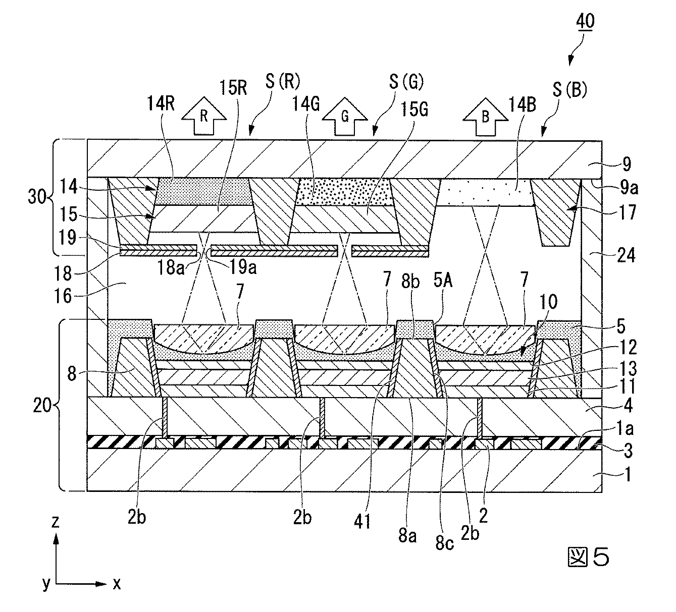
図5に示す本実施形態の有機EL装置40は、複数の有機発光素子10を区画する第1バンク8の側面に反射機能を付与した点において、上述した第1実施形態と異なる。
[Third embodiment]
Hereinafter, an organic EL device according to a third embodiment of the present invention will be described.
FIG. 5 is a cross-sectional view illustrating a schematic configuration of the organic EL device according to the third embodiment.
The
素子基板20側には、基板1上に、複数の有機発光素子10を区画する第1バンク8が設けられている。
本実施形態では、第1バンク8の側面8cに第2反射層41が設けられており、有機発光素子10から放出された光を集光部材7側へと反射させる構成となっている。第2反射層41は、上述した第1反射層19と同様の材料を用いて形成することが可能である。
On the
In the present embodiment, the second
このように、有機発光素子10を区画する第1バンク8の側面8cに第2反射層41を設けることによって、有機発光素子10から放射された光をより多く集光部材7へ入射させることが可能となる。
Thus, by providing the second
[第4実施形態]
以下、本発明の第4実施形態の有機EL装置について述べる。
図6は、第4実施形態の有機EL装置の概略構成を示す断面図である。
図6に示す本実施形態の有機EL装置50は、集光部材7と色変換層15(カラーフィルター層14)との間に、特定波長の光を透過させるバンドパスフィルター51が配置されている点において、上述した第1実施形態と異なる。
[Fourth embodiment]
The organic EL device according to the fourth embodiment of the present invention will be described below.
FIG. 6 is a cross-sectional view illustrating a schematic configuration of the organic EL device according to the fourth embodiment.
In the
バンドパスフィルター51は、RGBの各光をそれぞれ透過させる、赤色波長反射部51R、緑色波長透過部51G、青色波長透過部51Bを有して構成されている。
赤色波長反射部51Rは、赤色画素部S(R)における赤色蛍光体層15Rと、これに対向する集光部材7と、の間に配置されており、有機発光素子10からの青緑色光を透過するとともに、640nm〜720nmの波長域の光のみを選択的に反射させる。
The
The red
緑色波長透過部51Gは、緑色画素部S(G)における緑色蛍光体層15Gと、これに対向する集光部材7と、との間に配置されており、500nm〜560nmの波長域の光のみを選択的に透過させる。
The green
青色波長透過部51Bは、青色画素部S(B)におけるカラーフィルター層14の青色カラーフィルター14Bとの間に配置されており、435nm〜480nmの波長域の光のみを選択的に透過させる。
The blue
本実施形態における有機発光素子10は青緑色光を発光する。このため、バンドパスフィルター51において、緑色画素部S(G)及び青色画素部S(B)では、緑色波長透過部51G及び青色波長透過部51Bにおいて、緑色光、青色光をそれぞれ選択的に透過させる。一方、赤色画素部S(R)の赤色波長反射部51Rでは、有機発光素子10からの青緑色光をそのまま透過させる。そして、赤色波長反射部51Rを透過した青緑色光により赤色蛍光体層15Rが励起され、赤色光を発光する。赤色蛍光体層15Rから有機発光素子10側へ放射される光のほとんどは、遮光部材18上の第1反射層19により赤色蛍光体層15R側へと反射されるが、仮に、開口18a,19aを通じて有機発光素子10側へと漏れ出した光があったとしても、赤色波長反射部51Rにおいて赤色蛍光体層15Rへと反射されることになる。これにより、色滲みなく効率よく色変換層15に入射させることが可能となる。
The organic
なお、バンドパスフィルター51は、素子基板20側、波長変換基板30側のいずれに設けられていてもよい。例えば、素子基板20における封止層5上に配置されていてもよいし、波長変換基板30における遮光部材18の表面(第1反射層19とは反対側の面)上に配置されていてもよい。あるいは、不図示の支持手段を介して他の構成要素に固定されていてもよい。
The
[第5実施形態]
以下、第5実施形態の有機EL装置について述べる。
図7は、第5実施形態の有機EL装置の概略構成を示す断面図である。
図7に示す本実施形態の有機EL装置55は、波長変換基板30側に設けられる第2バンク42の形状が逆テーパー形状(先の実施形態における第2バンク17とはテーパー形状が上下逆向き)とされている点において、上述した第1実施形態と異なる。
[Fifth Embodiment]
Hereinafter, the organic EL device of the fifth embodiment will be described.
FIG. 7 is a cross-sectional view illustrating a schematic configuration of the organic EL device of the fifth embodiment.
In the
透明基板9上には、カラーフィルター層14を区画する第2バンク42が設けられている。本実施形態の第2バンク42は、透明基板9の一面9aに対向する第1端面42aと、第1端面42aに対向するとともに第1端面42aの面積よりも大きい面積を有する第2端面42bと、側面42cと、を有して構成されるもので、第1実施形態における第2バンク17とは上下方向を逆向きにした逆テーパー形状となっている。すなわち、透明基板9に対向する第1端面42aが第2端面42bよりも小さい面積を有する形状となっている。ここで、「逆テーパー形状」とは、透明基板9から離れる方向に断面形状が太くなるテーパー形状のことをいう。
On the
第2バンク42の第2端面42b上には、第2端面42bの全体を覆うようにして、第1反射層19と遮光部材18とが第2端面42bからこの順で設けられている。
On the
本実施形態の構成によれば、透明基板9に対向する第1端面42aが第2端面42bよりも小さい面積を有する逆テーパー形状の第2バンク42を設けることにより、上述した順テーパー形状の第2バンクを備える構成よりも有効画素領域を広くすることができる。これにより、開口率を高くすることが可能となり、表示特性の良好な有機EL装置55が得られる。
According to the configuration of the present embodiment, by providing the reverse tapered
[第6実施形態]
以下、第6実施形態の有機EL装置について述べる。
図8は、第6実施形態の有機EL装置の概略構成を示す断面図である。
図8に示す本実施形態の有機EL装置60は、第2バンク42の側面42cに反射機能を付与した点において、上述した第5実施形態と異なる。
[Sixth Embodiment]
The organic EL device according to the sixth embodiment will be described below.
FIG. 8 is a cross-sectional view illustrating a schematic configuration of the organic EL device according to the sixth embodiment.
The
本実施形態では、カラーフィルター層14を区画する第2バンク42の側面42cに第3反射層43が設けられており、色変換層15から放出された光を透明基板9側へと反射させる構成となっている。第3反射層43は、上述した第1反射層19と同様の材料を用いて形成することが可能である。
In the present embodiment, the third
このような構成によれば、色変換層15から等方的に放射された光の一部を第3反射層43により透明基板9側へと反射させることができる。第3反射層43と、色変換層15に対向して配置された第1反射層19との相乗効果により、光の取り出し効率をより向上させることが可能となる。
According to such a configuration, part of the light emitted isotropically from the
[第7実施形態]
以下、第7実施形態の有機EL装置について述べる。
図9は、第7実施形態の有機EL装置の概略構成を示す断面図である。
図9に示す本実施形態の有機EL装置70は、波長変換基板30側に複数の低屈折率層71を備えている点において上述した第1実施形態と異なる。
[Seventh embodiment]
Hereinafter, the organic EL device of the seventh embodiment will be described.
FIG. 9 is a cross-sectional view illustrating a schematic configuration of the organic EL device of the seventh embodiment.
The
低屈折率層71は、透明基板9、カラーフィルター層14、色変換層15のいずれよりも低い屈折率を有しており、サブ画素Sごとに1つあるいは2つずつ設けられている。具体的には、透明基板9の一面9aにおける第2バンク17によって区画された領域内であって、赤色カラーフィルター14R、緑色カラーフィルター14G、青色カラーフィルター14Bのそれぞれと透明基板9との間に設けられている。さらに、赤色画素部S(R)では、赤色カラーフィルター14Rと赤色蛍光体層15Rとの間にも低屈折率層71が配置され、緑色画素部S(G)では、緑色カラーフィルター14Gと緑色蛍光体層15Gとの間にも低屈折率層71が配置されている。
The low
図10は、波長変換基板における各構成要素の屈折率の関係を説明するための図である。
図10に示すように、透明基板9の屈折率は1.5、カラーフィルター層14の屈折率は1.6、色変換層15の屈折率は1.7である。これに対して、低屈折率層71の屈折率は、概ね1.0とされており、上下方向で隣り合う各層よりも小さい屈折率を有する。
FIG. 10 is a diagram for explaining the relationship between the refractive indexes of the components in the wavelength conversion substrate.
As shown in FIG. 10, the
低屈折媒質としては気体(屈折率が概ね1.0である媒体)であればよく、一例として空気、窒素、アルゴン、またはこれらの混合ガスが挙げられる。 The low refractive medium may be a gas (medium having a refractive index of approximately 1.0), and examples thereof include air, nitrogen, argon, or a mixed gas thereof.
一般的に、屈折率の大きい媒質から小さい媒質に光が進むときに全反射が発生し得る。
本実施形態の構成によれば、カラーフィルター層14及び透明基板9の光入射側にこれらよりも低い屈折率を有する低屈折率層71が設けられていることから、色変換層15からカラーフィルター層14へ光が入射する際や、カラーフィルター層14から透明基板9へ光が入射する際に全反射が起こりにくくなる。これにより、光学的な損失を抑えられ、光の取り出し効率の低減を防ぐことが可能である。
In general, total reflection can occur when light travels from a medium having a large refractive index to a medium having a small refractive index.
According to the configuration of the present embodiment, since the
なお、屈折率が概ね1.0の空気層を低屈折率層71としてもよい。空気層以外にも不活性ガス層や減圧層であってもよい。
An air layer having a refractive index of approximately 1.0 may be used as the low
[第8実施形態]
以下、第8実施形態の有機EL装置について述べる。
図11(A)は、第8実施形態の有機EL装置の概略構成を示す断面図である。
図11(A)に示す本実施形態の有機EL装置80は、素子基板20側における集光部材7と有機発光素子10との間に、平坦化層81と封止層82とを有する。
[Eighth embodiment]
The organic EL device according to the eighth embodiment will be described below.
FIG. 11A is a cross-sectional view illustrating a schematic configuration of the organic EL device of the eighth embodiment.
An
平坦化層81は、第1バンク8及び複数の有機発光素子10を覆い、これらの表面上を平坦にするものである。封止層82は、平坦化層81との密着性に優れた材料より構成されている。封止層82の表面上には複数の集光部材7がRGBのサブ画素Sごとに設けられており、各集光部材7は、対応する有機発光素子10の真上となる位置に配置されている。
The
集光部材7の固定方法は各種手段を用いることができる。例えば、不図示の接着剤を介して封止層82の表面に集光部材7が固定されていてもよいし、封止層82に凹部を形成し、当該凹部内に集光部材7を収容するように構成してもよい。あるいは、複数の集光部材7を有するレンズシートを封止層82上に貼り合せるようにしてもよい。
Various means can be used for fixing the
また、平坦化層81及び封止層82の層厚を変化させて集光部材7の焦点位置を調整するようにしてもよい。
Further, the focal position of the
図11(B)は、集光部材としてレンズシートを備えた構成を示す断面図である。
図11(B)に示すように、集光部材として平面視が円形状とされた複数のマイクロレンズ23からなるレンズシート45を封止層82上に備えてもよい。レンズシート45は、封止層82に対して不図示の接着層などを介して貼り合わされる。このとき、サブ画素Sごとに同じ個数のマイクロレンズ23が配置されるようにレンズシート45を貼り合せることが好ましい。
FIG. 11B is a cross-sectional view illustrating a configuration including a lens sheet as a light collecting member.
As shown in FIG. 11B, a
[第9実施形態]
以下、第9実施形態の有機EL装置について述べる。
図12は、第9実施形態の有機EL装置の構成を示す概念図である。
図12に示す本実施形態の有機EL装置90は、透明基板9上に、カラーフィルター層14、色変換層15及びバンドパスフィルター51が積層されている点において先の実施形態とは異なる。
[Ninth Embodiment]
The organic EL device according to the ninth embodiment will be described below.
FIG. 12 is a conceptual diagram showing the configuration of the organic EL device of the ninth embodiment.
The
本実施形態では、カラーフィルター層14、色変換層15及びバンドパスフィルター51が、透明基板9上に形成された第2バンク97内に収容された構成となっている。
具体的に、赤色画素部S(R)では、透明基板9上に、赤色カラーフィルター14R、赤色蛍光体層15R、赤色波長反射部51Rがこの順に積層されている。緑色画素部S(G)では、透明基板9上に、緑色カラーフィルター14G、緑色蛍光体層15G、緑色波長透過部51Gがこの順に積層されている。青色画素部S(B)では、青色カラーフィルター14B上に青色波長透過部51Bが積層されている。
In the present embodiment, the
Specifically, in the red pixel portion S (R), a
各集光部材7の焦点位置は、色変換層15と集光部材7との間であって、バンドパスフィルター51と集光部材7との間にそれぞれ位置していることがより好ましい。
It is more preferable that the focal position of each light collecting
この構成によれば、透明基板9上に、カラーフィルター層14、色変換層15及びバンドパスフィルター51を連続して形成することができるので製造が容易となる。
なお、カラーフィルター層14、色変換層15及びバンドパスフィルター51のそれぞれの境界部分に上述した低屈折率層が設けられていてもよい。
According to this configuration, the
In addition, the low refractive index layer mentioned above may be provided in each boundary part of the
[第10実施形態]
以下、第10実施形態の有機EL装置について述べる。
図13は、第10実施形態の有機EL装置の構成を示す概念図である。
図13に示す本実施形態の有機EL装置110は、カラーフィルター層14と色変換層15との間に集光部材7が配置されている点において、先の実施形態とは異なる。
[Tenth embodiment]
Hereinafter, the organic EL device of the tenth embodiment will be described.
FIG. 13 is a conceptual diagram showing the configuration of the organic EL device of the tenth embodiment.
The
有機EL装置110では、色変換層15とカラーフィルター層14とが互いに離間して配置されており、色変換層15のカラーフィルター層14側の面に複数の集光部材7が固定されている。集光部材7とカラーフィルター層14との間には充填層(第2充填層)46が充填されている。充填層46は、素子基板20と波長変換基板30との間(封止層5と色変換層15との間)に充填された充填層16と同様の構成とされている。
In the
本実施形態における色変換層15は、赤色蛍光体層15R、緑色蛍光体層15Gの他に、入射した光をそのままの波長で射出させる透明な無変換層15Cを有する。青色画素部S(B)に対応して設置される集光部材7は、透明な無変換層15Cの表面上に固定される。集光部材7の固定には、接着剤以外にも、種々の手段を利用することができる。
In addition to the
また、色変換層15の支持構造についても特に限定はしないが、例えば、カラーフィルター層14を区画する第2バンク97の高さを高く形成しておき、第2バンク97に対して色変換層15を固定してもよい。第2バンク97の高さを、カラーフィルター層14との色変換層15との間に集光部材7を配置できる高さとし、カラーフィルター層14に光が入射する前に集光部材7の焦点が結ぶように構成する。
The support structure of the
なお、集光部材7の焦点位置が、カラーフィルター層14と集光部材7との間となるように、集光部材7の配置場所や集光部材7の大きさ等を選定する。
The location of the
本実施形態では、透明基板9の面9bに、不図示の接着層を介して光散乱部材92が設けられている。
光散乱部材92は、バインダー樹脂93の内部に複数の光散乱体94が分散されてなるものである。バインダー樹脂93としては、例えばアクリル樹脂等が用いられる。光散乱体94としては、例えばアクリルビーズ等が用いられる。
In the present embodiment, a
The
光散乱部材92は、光を異方的に散乱させるものであってもよいし、光を等方的に散乱させるものであってもよい。光散乱部材92の使用により、カラーフィルター層14を射出した光を十分に拡散させることができる。
The
なお、光散乱体94として、アクリルビーズ以外にもプリズム等を利用することができる。
In addition to the acrylic beads, a prism or the like can be used as the
本実施形態のように、色変換層15の光射出面側に集光部材7を配置する場合には、集光部材7の光軸上に設けた光散乱部材92により集光部材7の透過光を散乱させることで、ランバーシアン発光が得られる。
When the
[第11実施形態]
以下、第11実施形態の有機EL装置について述べる。
図14は、第11実施形態の有機EL装置の構成を示す概念図である。
図14に示す本実施形態の有機EL装置120は、カラーフィルター層14から離間して配置された色変換層15と遮光部材98とが一体とされている点において先の実施形態とは異なる。
[Eleventh embodiment]
Hereinafter, the organic EL device of the eleventh embodiment will be described.
FIG. 14 is a conceptual diagram showing the configuration of the organic EL device of the eleventh embodiment.
The
本実施形態における色変換層15は、カラーフィルター層14から所定の間隔をおいて配置され、透明基板9の一面9aに形成された上述の第2バンク97上に設けられている。赤色蛍光体層15R及び緑色蛍光体層15Gを有する色変換層15の一面15a(カラーフィルター層14側と反対側の面)には遮光部材98が設けられており、赤色蛍光体層15R及び緑色蛍光体層15Gのそれぞれに対応した2つの開口98aを有している。赤色画素部S(R)及び緑色画素部S(G)に配置された各集光部材7の焦点は、上記した遮光部材98の開口98a内にそれぞれ位置している。なお、青色画素部S(B)の集光部材7の焦点位置は、集光部材7と青色カラーフィルター14B(カラーフィルター層14)との間に位置する。
The
また、遮光部材98は反射性を有しており、色変換層15に接している面が反射面98Bとなっている。
Further, the
有機発光素子10から放出された光は、まず集光部材7により集光され、遮光部材98の開口98aを通じて色変換層15に入射して赤色あるいは緑色に色変換された後、カラーフィルター層14においてさらに色調が高められて透明基板9から射出する。このとき、色変換層15において等方的に放射された光を、遮光部材98の反射面98Bにより色変換層15内へと再び入射させることができるため、有機発光素子10側へ光が漏れ出すことが防止される。
The light emitted from the organic
なお、色変換層15の支持構造については上述したものに限らない。
Note that the support structure of the
[第12実施形態]
以下、第12実施形態の有機EL装置について述べる。
図15は、第12実施形態の有機EL装置の概略構成を示す断面図である。
図15に示す本実施形態の有機EL装置130は、カラーフィルター層14を区画する逆テーパー形状の第2バンク99の第2端面99b(透明基板9とは反対側の端面)に、遮光部材18と色変換層15とが積層されている点において、先の実施形態とは異なる。
[Twelfth embodiment]
Hereinafter, an organic EL device according to a twelfth embodiment will be described.
FIG. 15 is a cross-sectional view illustrating a schematic configuration of the organic EL device according to the twelfth embodiment.
The
透明基板9上には、カラーフィルター層14を区画する第2バンク99が設けられている。この第2バンク99は、上述したように、透明基板9の一面9aに対向する第1端面99aと、第1端面99aに対向するとともに第1端面99aの面積よりも大きい面積を有する第2端面99bと、側面99cと、を有して構成されたものである。すなわち、透明基板9に対向する第1端面99aが第2端面99bよりも小さい面積を有する構造となっている。
A
第2バンク99の第2端面99b上には、第2端面99bの全体を覆うようにして、反射性を有する遮光部材98が設けられている。遮光部材98の一面(第2端面99bに接する面)は反射面98Bである。
On the
遮光部材98の反射面98Bとは反対側の面上には、赤色画素部S(R)及び緑色画素部S(G)に対応する箇所に、赤色蛍光体層15R及び緑色蛍光体層15Gがそれぞれ配置されている。
集光部材7の焦点位置は、遮光部材98の開口98a内に位置していてもよいし、色変換層15内に位置していてもよい。しかしながら、色変換層15の劣化を抑えるため、色変換層15と集光部材7との間に集光部材7の焦点が位置していることがより好ましい。
On the surface opposite to the
The focal position of the
本実施形態の構成によれば、第2バンク99と同時に、開口98aを有する遮光部材98をパターン形成することができるため、製造が容易である。
According to the configuration of the present embodiment, since the
[第13実施形態]
以下、第13実施形態の有機EL装置について述べる。
図16は、第13実施形態の有機EL装置の概略構成を示す断面図である。
図16に示す本実施形態の有機EL装置140は、有機発光素子10が集光部材7の曲面に沿って湾曲しており、この湾曲した有機発光素子10上に集光部材7が配置されている点において、先の実施形態と異なる。
[Thirteenth embodiment]
Hereinafter, an organic EL device according to a thirteenth embodiment will be described.
FIG. 16 is a cross-sectional view illustrating a schematic configuration of an organic EL device according to a thirteenth embodiment.
In the
本実施形態では、基板1上に、層間絶縁膜3及び平坦化膜4を介して第1バンク48が形成されている。第1バンク48は、サブ画素Sごとに設けられた複数の凹部49を有しており、各凹部49内に有機発光素子10と集光部材7とがそれぞれ収容されている。
In the present embodiment, the
有機発光素子10は、第1バンク48の凹部49内に蒸着法を用いて形成され、集光部材7における光入射面7aの曲率に応じた湾曲形状を成す。
集光部材7は、湾曲した有機発光素子10上に搭載され、光入射面7a側が有機発光素子10の第2電極12に対して固定されている。
なお、有機発光素子10と集光部材7との間に、有機発光素子10を封止する封止層が設けられていてもよい。
The organic
The condensing
Note that a sealing layer for sealing the organic
このような構成とすることにより、基板1に対する集光部材7のアライメントが行い易くなり、集光部材7の配置作業を短時間で効率よく行うことができる。
With such a configuration, it is easy to align the
[第14実施形態]
以下、第14実施形態の有機EL装置について述べる。
図17は、第14実施形態の有機EL装置の概略構成を示す断面図である。
図17に示す本実施形態の有機EL装置150は、球体の集光部材27を備えている点において、先の実施形態と異なる。
球体を成す複数の集光部材27は、素子基板20側の封止層5に設けられた各凹部5A内に収容されている。
[Fourteenth embodiment]
The organic EL device according to the fourteenth embodiment will be described below.
FIG. 17 is a cross-sectional view illustrating a schematic configuration of the organic EL device according to the fourteenth embodiment.
The
A plurality of condensing
[第15実施形態]
以下、第15実施形態の有機EL装置について述べる。
図18は、第15実施形態の有機EL装置の概略構成を示す断面図である。
図18に示す本実施形態の有機EL装置160は、集光部材として、先端をレンズ状にした光ファイバー(集光レンズ)28を備えている点において、先の実施形態と異なる。
光ファイバー28は、先端にレンズ形状とされた集光面28Aを有しており、遮光部材18の開口18a部分に固定されている。
有機発光素子10から放射された光は、光ファイバー28の導光部28b内を導光した後、集光面28Aにおいて集光されて射出する。
[Fifteenth embodiment]
The organic EL device according to the fifteenth embodiment is described below.
FIG. 18 is a cross-sectional view illustrating a schematic configuration of the organic EL device according to the fifteenth embodiment.
An
The
The light emitted from the organic
[第16実施形態]
以下、第16実施形態の有機EL装置について述べる。
図19は、第16実施形態の有機EL装置の概略構成を示す断面図である。
図19に示す本実施形態の有機EL装置170は、透明基板9上に設けられた「順テーパー形状」の第2バンク17の側面17cに第3反射層43が設けられている点において、先の実施形態と異なる。
上述したように、「順テーパー形状」とは、透明基板9から離れる方向に断面形状が細くなるテーパー形状のことを言い、このような第2バンク17は、透明基板9に対向する第1端面17aと、第1端面17aに対向して第1端面17aの面積よりも小さい面積を有する第2端面17bと、側面17cと、を有している。
[Sixteenth embodiment]
The organic EL device according to the sixteenth embodiment will be described below.
FIG. 19 is a cross-sectional view illustrating a schematic configuration of the organic EL device according to the sixteenth embodiment.
The
As described above, the “forward taper shape” means a taper shape whose cross-sectional shape becomes narrower in a direction away from the
本実施形態の構成によれば、第2バンク17の側面17cに設けた第3反射層43により、色変換層15、カラーフィルター層14から放出された光を、第1反射層19を介して透明基板9側へと反射させることができる。つまり、色変換層15、カラーフィルター層14から放出された光の一部は、第3反射層43によって第1反射層19側へと反射され、さらに第1反射層19によって透明基板9側へと反射されることになる。
また、色変換層15カラーフィルター層14から放出された光のうち第1反射層19へと直接入射した光は、当該第1反射層19によって透明基板9側へと反射される。このように、色変換層15に対向して配置された第1反射層19との相乗効果によって、光の取り出し効率をより向上させることが可能となる。
According to the configuration of the present embodiment, the third
The light directly incident on the first
なお、第2バンク17の側面17cだけでなく、第1バンク8の側面8cにも反射層を設けた構成としてもよい。これにより、より一層高輝度な有機EL装置が得られる。また、第2バンク17を可視光を透過しないブラックマトリクスにより構成することで、コントラストの向上が図れる。
In addition, the reflection layer may be provided not only on the
[第17実施形態]
以下、第17実施形態の有機EL装置について述べる。
図20は、第17実施形態の有機EL装置の概略構成を示す断面図である。
図20に示す本実施形態の有機EL装置180は、透明基板9上に設けられた「逆テーパー形状」の第2バンク42の側面42cに第3反射層43が設けられているとともに、基板1上に設けられた「順テーパー形状」の第1バンク8の側面8cにも第2反射層41が設けられていた構成となっている。本実施形態は、第1バンク8の側面8cに第2反射層41が設けられている点において、先の第6実施形態の構成と異なっている。
[Seventeenth embodiment]
The organic EL device according to the seventeenth embodiment will be described below.
FIG. 20 is a cross-sectional view illustrating a schematic configuration of the organic EL device according to the seventeenth embodiment.
In the
本実施形態では、基板1上に設けられた順テーパー形状の第1バンク8の側面8cに第2反射層41が設けられている。
In the present embodiment, the second
一方、透明基板9上に設けられた「逆テーパー形状」の第2バンク42の側面42cには、第3反射層43が設けられている。第3反射層43は、第2バンク42の側面42c全体に設けられている。
On the other hand, a third
本実施形態の構成によれば、有機発光素子10を区画する第1バンク8の側面8cに設けた第2反射層41により、有機発光素子10から放射された光をより多く集光部材7へ入射させることが可能となる。
According to the configuration of the present embodiment, the second
また、第2バンク42の側面42c設けられた第3反射層43により、色変換層15から等方的に放射された光の一部を積極的に透明基板9側へと反射させることができる。このため、第3反射層43と、色変換層15に対向して配置された第1反射層19との相乗効果により、光の取り出し効率をより向上させることが可能となる。
In addition, the third
以上、添付図面を参照しながら本発明に係る好適な実施形態について説明したが、本発明は係る例に限定されないことは言うまでもない。当業者であれば、特許請求の範囲に記載された技術的思想の範疇内において、各種の変更例または修正例に想到し得ることは明らかであり、それらについても当然に本発明の技術的範囲に属するものと了解される。 As described above, the preferred embodiments according to the present invention have been described with reference to the accompanying drawings, but the present invention is not limited to the examples. It is obvious for those skilled in the art that various changes or modifications can be conceived within the scope of the technical idea described in the claims. It is understood that it belongs to.
例えば、上述した各実施形態においては、カラーフィルター層14を備えた構成について述べたが、図21に示すように、必ずしも透明基板9上にカラーフィルター層14が設けられていなくてもよい。例えば、透明基板9の一面9a上に色変換層15が直接形成された構成としてもよい。
For example, in each of the above-described embodiments, the configuration including the
また、集光部材として、複数のレンズの光軸を互いに一致させて並設した構成としてもよい。 Further, the condensing member may have a configuration in which the optical axes of a plurality of lenses are arranged in parallel with each other.
また、上述した各実施形態の構成は、発光層に有機材料を用いた他の有機発光装置や、その他の発光装置の構成にも応用することができる。 The configuration of each embodiment described above can also be applied to other organic light emitting devices using an organic material for the light emitting layer and other light emitting devices.
なお、上述した各実施形態に限られず、各実施形態における構成を適宜組み合わせても構わない。 In addition, it is not restricted to each embodiment mentioned above, You may combine the structure in each embodiment suitably.
更に、下記に示す実施例により本発明を詳細に説明するが、本発明はこれらの例によってなんら限定されるものではない。 Further, the present invention will be described in detail with reference to the following examples, but the present invention is not limited to these examples.
<波長変換基板の作製>
以下、本発明における実施例1を説明する。
図22は、実施例1における有機EL装置200の概略構成を示す図である。
透明基板9として、100×100mm角、0.7mm厚のガラスを用いた。これを水洗後、純水超音波洗浄10分、アセトン超音波洗浄10分、イソプロピルアルコール蒸気洗浄5分を行い、100℃にて1時間乾燥させた。
<Production of wavelength conversion substrate>
FIG. 22 is a diagram illustrating a schematic configuration of the
As the
まず、黒色隔壁である第2バンク17の材料として、東京応化製のBKレジストを、スピンコーターを用いて塗布した。その後、70℃で15分間プリベークして膜厚1μmの塗膜を形成した。この塗膜に所望の画像パターンが形成できるようなマスク(画素ピッチ200μm、線幅20μm)を被せてi線(100mJ/cm2)を照射し、露光した。
First, a BK resist made by Tokyo Ohka Co., Ltd. was applied using a spin coater as a material for the
次いで、現像液として炭酸ナトリウム水溶液を用いて現像し、純水でリンス処理を行い、光吸収層26(低反射層)を得た。 Subsequently, it developed using the sodium carbonate aqueous solution as a developing solution, rinsed with the pure water, and obtained the light absorption layer 26 (low reflection layer).
次に、第2バンク17の材料として、エポキシ系樹脂(屈折率:1.59)、アクリル系樹脂(屈折率:1.49)、ルチル型酸化チタン(屈折率:2.71、粒径250nm)、光重合開始剤、芳香族系溶剤からなる白色感光性組成物を攪拌混合してポジ型レジストを用意した。そして、上記した透明基板9上に、このポジ型レジストをスピンコーターを用いて塗布した。画素ピッチ200μm、線幅20μmでパターン形成し、上記した光吸収層26上に膜厚5μmの光反射性を有する第2バンク17を作製した。
Next, as a material for the
次に、第2バンク17によって区画された領域に、赤色カラーフィルター14R、緑色カラーフィルター14G、青色カラーフィルター14Bをパターン形成した。
Next, a
次に、青色画素部S(B)、緑色画素部S(G)には、青色散乱層32B、緑色散乱層32Gを形成する。青色散乱層32B及び緑色散乱層32Gの形成には、まず、1.5μmのシリカ粒子(屈折率:1.65)20gを、水/ジメチルスルホキシド=1/1の混合溶液(300g)で溶解されたポリビニルアルコールを30g加え、分散機により攪拌して散乱層形成用塗液を作製した。
Next, a
作製した散乱層形成用塗液を、スクリーン印刷法で、透明基板9上の光吸収層26を形成していない領域に塗布した。引き続き、真空オーブン(200℃、10mmHgの条件)で4時間加熱乾燥し、青色散乱層32B及び緑色散乱層32G(これらを単に散乱層32と言うこともある)を形成した。
The produced scattering layer forming coating solution was applied to a region on the
次に、ポリスチレン樹脂(10g)に9−(1H−ベンゾイミダゾール−2−イル)−1,1,6,6−テトラメチル−2,3,5,6−テトラヒドロ−1H,4H−11−オキサ−アザ−ベンゾアントラセン−10−ワン(1g)とルモーゲンレッド(0.1g)をトルエンに溶解させ波長変換層形成塗液を作製した。 Next, 9- (1H-benzoimidazol-2-yl) -1,1,6,6-tetramethyl-2,3,5,6-tetrahydro-1H, 4H-11-oxa was added to polystyrene resin (10 g). -Aza-benzoanthracene-10-one (1 g) and lumogen red (0.1 g) were dissolved in toluene to prepare a wavelength conversion layer forming coating solution.
次に、透明基板9のカラーフィルター層14上に、色変換層形成塗液をスピンコート法を用いて塗布し、2μmの膜厚の色変換層15を形成する。
Next, a color conversion layer forming coating solution is applied on the
次に、色変換層15における青色画素部S(B)、緑色画素部S(B)に対応する部分は光を透過し、赤色画素部S(R)に対応する部分は遮光するように設計されたフォトマスクを用いて、色変換層15に対して透明基板9と逆側から超高圧UVランプを照射した。
これにより青色画素部S(B)及び緑色画素部S(G)においては、色変換層15の青色光領域、緑色光領域での吸収率を低下させ、かつ、赤色波長変換機能を低下させた。これにより、赤色発光を非発光に変性させており、有機発光素子10からの発光をそのまま効率良く透過させ、かつ、赤色成分の発光の混じりによる色純度の低下を防止する事が出来る。上記プロセスは、ドライエアー中で行った。
Next, the portion corresponding to the blue pixel portion S (B) and the green pixel portion S (B) in the
Thereby, in blue pixel part S (B) and green pixel part S (G), the absorptance in the blue light area | region of the
次に、透明基板9を、グローブボックス(水分濃度:1ppm以下、酸素濃度:1ppm以下)に移し、80℃、1h加熱し、膜中の水分、酸素を除去した。
次に、スパッタ蒸着により、膜厚2μmのSiON 膜からなるガスバリア層を形成し、Sを作製した。
Next, the
Next, a gas barrier layer made of a SiON film having a thickness of 2 μm was formed by sputter deposition, and S was produced.
<素子基板の作製>
(アクティブマトリクス基板)
100×100mm角、0.7mm厚のガラス基板から成る基板1上に、PECVD法を用いて、アモルファスシリコン半導体膜を形成する。続いて、結晶化処理を施すことにより多結晶シリコン半導体膜を形成する。
<Production of element substrate>
(Active matrix substrate)
An amorphous silicon semiconductor film is formed on the
次に、フォトリソグラフィー法を用いて多結晶シリコン半導体膜を複数の島状にパターンニングする。続いて、パターニングした多結晶シリコン半導体層の上にゲート絶縁膜及びゲート電極層をこの順番で形成し、フォトリソグラフィー法を用いてパターニングを行った。 Next, the polycrystalline silicon semiconductor film is patterned into a plurality of islands using a photolithography method. Subsequently, a gate insulating film and a gate electrode layer were formed in this order on the patterned polycrystalline silicon semiconductor layer, and patterning was performed using a photolithography method.
その後、パターニングした多結晶シリコン半導体膜にリン等の不純物元素をドーピングすることによりソース及びドレイン領域を形成し、TFT素子を作製した。その後、平坦化膜を形成した。平坦化膜としては、PECVD法で形成した窒化シリコン膜、スピンコーターでアクリル系樹脂層をこの順で積層し形成する。まず、窒化シリコン膜を形成した後、窒化シリコン膜とゲート絶縁膜とを一括してエッチングすることによりソース及び/又はドレイン領域に通ずるコンタクトホールを形成し、続いて、ソース配線を形成した。 Thereafter, the patterned polycrystalline silicon semiconductor film was doped with an impurity element such as phosphorus to form source and drain regions, and a TFT element was fabricated. Thereafter, a planarizing film was formed. As the planarizing film, a silicon nitride film formed by PECVD and an acrylic resin layer are formed in this order by a spin coater. First, after forming a silicon nitride film, the silicon nitride film and the gate insulating film were etched together to form a contact hole leading to the source and / or drain region, and then a source wiring was formed.
その後、アクリル系樹脂層を形成し、ゲート絶縁膜及び窒化シリコン膜に穿孔したドレイン領域のコンタクトホールと同じ位置に、ドレイン領域に通ずるコンタクトホールを形成することにより、アクティブマトリクス基板が完成する。平坦化膜としての機能は、アクリル系樹脂層で実現される。なお、TFTのゲート電位を定電位にするためのコンデンサーは、スイッチング用TFTのドレインと駆動用TFTのソースとの間に層間絶縁膜等の絶縁膜を介することで形成される。 Thereafter, an acrylic resin layer is formed, and a contact hole leading to the drain region is formed at the same position as the contact hole of the drain region drilled in the gate insulating film and the silicon nitride film, thereby completing the active matrix substrate. The function as a planarizing film is realized by an acrylic resin layer. Note that the capacitor for setting the gate potential of the TFT to a constant potential is formed by interposing an insulating film such as an interlayer insulating film between the drain of the switching TFT and the source of the driving TFT.
アクティブマトリクス基板25には、平坦化膜4を貫通し、駆動用TFTと、後に形成する有機発光素子10の第1電極11とをそれぞれ電気的に接続するコンタクトホール2bが設けられている。
The
(有機発光素子の作製)
まず、各画素を駆動する為のTFTと電気的に接続する第1電極11(陽極)を形成する。有機発光素子10の第1電極11とTFTとは、平坦化膜4を貫通して設けられたコンタクトホール2bを介して接続されている。
第1電極11は、スパッタ法を用いて、反射電極Al(アルミニウム)を150nmと透明電極IZO(酸化インジウム−酸化亜鉛)を90nmの膜厚で積層して形成し、青色画素部S(B)、赤色画素部S(R)に対応した形状に、従来のフォトリソグラフィー法でパターン化する。
(Preparation of organic light emitting device)
First, a first electrode 11 (anode) that is electrically connected to a TFT for driving each pixel is formed. The
The
更に、スパッタ法により反射電極Al(アルミニウム)を150nmと透明電極IZO(酸化インジウム−酸化亜鉛)を180nmの膜厚で積層して形成し、緑色画素部S(G)に対応した形状に従来のフォトリソグラフィー法でパターン化する。
これにより、青色画素部S(B)と緑色画素部S(G)の透明電極の膜厚を変える事で、反射電極と半透明電極の間での干渉(マイクロキャビティー)効果による色純度の強調を行う事が可能となる。
Further, the reflective electrode Al (aluminum) 150 nm and the transparent electrode IZO (indium oxide-zinc oxide) with a film thickness of 180 nm are formed by sputtering to form a conventional shape into a shape corresponding to the green pixel portion S (G). Patterning is performed by photolithography.
As a result, the color purity due to the interference (microcavity) effect between the reflective electrode and the semi-transparent electrode is changed by changing the film thickness of the transparent electrode of the blue pixel portion S (B) and the green pixel portion S (G). Emphasis can be made.
ここでは、第1電極11の面積を、180μm×540μmとした。また、ガラス基板からなる基板1の周辺部には、2mm幅の封止エリア44が設けられている。基板1の短辺方向両側には、封止エリア44よりも外側にそれぞれ2mmの端子取出し部(不図示)が設けてある。長辺方向一方には、2mmの端子取出し部(不図示)が設けている。
Here, the area of the
次に、第1電極11上に、先に述べた第2バンク17の形成材料と同様のTiO2を含有する感光性樹脂をスピンコート法より200nm積層し、従来のフォトリソグラフィー法により、第1電極11のエッジ部を覆うようにパターン化した。ここでは、第1電極11の4辺を覆うとともに、各辺の周縁部から内側に10μmの領域を覆うエッジカバー33とした。
Next, a photosensitive resin containing TiO 2 similar to the material for forming the
次に、アクティブマトリクス基板25を洗浄する。アクティブマトリクス基板25の洗浄としては、例えば、アセトン、IPAを用いて、超音波洗浄を10分間行い、次に、UV−オゾン洗浄を30分間行う。
Next, the
次に、アクティブマトリクス基板25をインライン型抵抗加熱蒸着装置内の基板ホルダーに固定し、1×10⁻⁴Pa以下の真空まで減圧し、各有機層の成膜を行った。
Next, the
まず、正孔注入材料として、1,1‐ビス-ジ-4−トリルアミノ‐フェニル-シクロヘキサン(TAPC)を用い抵抗加熱蒸着法により膜厚20nmの正孔注入層を形成した。
次に正孔輸送材料として、N,N‘−di−l-ナフチル-N,N’‐ジフェニル-1,1‘−ビフェニル-1,1’-ビフェニル-4,4‘-ジアミン(NPD)を用い抵抗加熱蒸着法により膜厚20nmの正孔輸送層を形成した。
First, as a hole injection material, 1,1-bis-di-4-tolylamino-phenyl-cyclohexane (TAPC) was used to form a hole injection layer having a thickness of 20 nm by resistance heating vapor deposition.
Next, N, N′-di-1-naphthyl-N, N′-diphenyl-1,1′-biphenyl-1,1′-biphenyl-4,4′-diamine (NPD) is used as a hole transport material. A 20 nm thick hole transport layer was formed by resistance heating vapor deposition.
次いで、正孔輸送層の上に青色有機発光層(厚さ:20nm)を形成する。この青色有機発光層は、1,4‐ビス-トリフェニルシリル−ベンゼン(UGH−2)(ホスト材料)とビス[(4,6−ジフルオロフェニル)‐ピリジナト‐N,C2‘]ピコリネート イリジウム(3)(FIrpic)(青色燐光発光ドーパント)をそれぞれの蒸着速度を1.5Å/sec、0.2Å/ secとし、共蒸着することで作製した。 Next, a blue organic light emitting layer (thickness: 20 nm) is formed on the hole transport layer. This blue organic light-emitting layer consists of 1,4-bis-triphenylsilyl-benzene (UGH-2) (host material) and bis [(4,6-difluorophenyl) -pyridinato-N, C2 ′] picolinate iridium (3 ) (FIrpic) (blue phosphorescent light emitting dopant) was prepared by co-evaporation at a deposition rate of 1.5 Å / sec and 0.2 Å / sec.
次いで、青色有機発光層の上に2,9‐ジメチルー4,7‐ジフェニル‐1,10‐フェナントロリン(BCP)を用いて正孔防止層(厚さ:10nm)を形成する。
次いで、正孔防止層の上にトリス(8‐ヒドロキシキノリン)アルミニウム(Alq3)を用いて電子輸送層(厚さ:10nm)を形成する。
Next, a hole blocking layer (thickness: 10 nm) is formed on the blue organic light emitting layer using 2,9-dimethyl-4,7-diphenyl-1,10-phenanthroline (BCP).
Next, an electron transport layer (thickness: 10 nm) is formed on the hole blocking layer using tris (8-hydroxyquinoline) aluminum (Alq3).
次いで、電子輸送層の上にフッ化リチウム(LiF)を用いて電子注入層(厚さ:0.5nm)を形成する。 Next, an electron injection layer (thickness: 0.5 nm) is formed on the electron transport layer using lithium fluoride (LiF).
この後、第2電極12として半透明電極を形成する。
まず、アクティブマトリクス基板25を金属蒸着用チャンバーに固定する。
次に、電子注入層上に真空蒸着法によりマグネシウムと銀をそれぞれ0.1Å/sec0.9Å/secの割合の蒸着速度で共蒸着によりマグネシウム銀を所望のパターンで形成(厚さ:1nm)する。
更にその上に、干渉効果を強調する目的、及び第2電極12での配線抵抗による電圧降下を防止する目的で、銀を1Å/secの蒸着速度で銀を所望のパターンで形成(厚さ:19nm)する。
これにより、有機発光素子10の第2電極12が形成される。ここで、有機発光素子10としては、第1電極11と第2電極12との間でマイクロキャビティ効果(干渉効果)が、発現し、正面輝度を高める事が可能となり有機発光素子10からの発光エネルギーをより効率良く、色変換層15、及び散乱層32に伝搬させることが可能となる。
ここで、マイクロキャビティー効果により、有機発光素子10からの発光の色純度(0.14、0.29)を、青色画素部S(B)、赤色画素部S(R)では色純度(0.14、0.08)に緑色画素部S(G)では色純度(0.27、0.64)に調整している。
Thereafter, a semitransparent electrode is formed as the
First, the
Next, magnesium and silver are formed in a desired pattern (thickness: 1 nm) on the electron injection layer by co-evaporation with magnesium and silver at a deposition rate of 0.1 Å / sec 0.9 Å / sec, respectively, by vacuum deposition. .
Furthermore, for the purpose of emphasizing the interference effect and preventing the voltage drop due to the wiring resistance at the
Thereby, the
Here, due to the microcavity effect, the color purity (0.14, 0.29) of light emission from the organic
次に、プラズマCVD法により、3μmのSiO2からなる無機保護層を、シャドーマスクを用いて表示部の端から上下左右2mmの封止エリア44までパターニングし、封止層5を形成する。以上により、アクティブ駆動型の素子基板20を作製する。
Next, an inorganic protective layer made of 3 μm of SiO 2 is patterned from the edge of the display portion to the sealing
この封止層5上に集光部材7を形成する。集光部材7は有機発光素子10上に配置される。集光部材7は、インクジェット法により、フッ素径樹脂や酸化チタンなどの無機ナノ粒子を混入したアクリル樹脂を用いてサブ画素Sごとにパターニング形成した。
次に、アクティブ駆動型の素子基板20と波長変換基板30とを、基板貼り合わせ用のグローブボックス(水分濃度:1ppm以下、酸素濃度:1ppm以下)に搬入する。
A condensing
Next, the active drive
次に、波長変換基板30の周縁部に、ディスペンサーを用いて、20μmのスペーサーを分散させた紫外線硬化型接着剤(スリーボンド社製、商品名30Y−437) を塗布した。
更に、シール部材24の内側に、ディスペンサーを用いて、透明シリコーン樹脂(東芝シリコーン社製、TSE3051) を充填し、充填層(第1充填層)29を形成した。
Next, an ultraviolet curable adhesive (trade name 30Y-437, manufactured by ThreeBond Co., Ltd.) in which a 20 μm spacer was dispersed was applied to the peripheral edge of the
Further, the inside of the
次に、アクティブ駆動型の素子基板20と波長変換基板30とを、真空チャンバ内に移送し、真空チャンバを1Paまで減圧した。そして、アライメントマーカーを用いて一次アライメントを行いながら、素子基板20と波長変換基板30との仮接着を行い、固定した。
Next, the active drive
次に、グローブボックスに移送し、CCDを用いて二次アライメントを行った。
続いて、UVランプを用いて、紫外線を照射して、紫外線硬化型接着剤を硬化させてシール部材24を形成した。
Next, it transferred to the glove box and secondary alignment was performed using CCD.
Subsequently, the sealing
次に、60分間にわたる80℃での加熱処理を行い、シール部材24、素子基板20及び波長変換基板30によって囲まれた空間内に充填された透明シリコーン樹脂をゲル化させた。
Next, heat treatment was performed at 80 ° C. for 60 minutes to gel the transparent silicone resin filled in the space surrounded by the
次に、波長変換基板30の透明基板9の外面(カラーフィルター層14を有する面9aとは反対側の面)に、不図示の偏光板を貼り合わせる。
Next, a polarizing plate (not shown) is bonded to the outer surface of the
最後に、基板1の短辺方向に形成された不図示の端子取り出し部をソースドライバを介して電源回路に接続し、長辺方向に形成された不図示の端子取り出し部をゲートドライバを介して外部電源に接続する。
Finally, a terminal extraction portion (not shown) formed in the short side direction of the
以上により、80×80mmの表示部52を有するアクティブ駆動型の有機EL装置200が完成する。ここで、外部電源により所望の電流を各画素に印加することで青緑色燐光を発光する有機発光素子10を任意にスイッチング可能な励起光源としている。
As a result, the active drive type
赤色画素部S(R)においては、赤色蛍光体層15Rにより、有機発光素子10からの発光をマイクロキャビティー効果による青緑色光から赤色に変換し、赤色変換光を更に赤色カラーフィルター14Rを透過させることにより赤色純度を向上させている。
In the red pixel portion S (R), the
緑色画素部S(G)においては、緑色蛍光体層15Gにより、有機発光素子10からの青緑色光から緑色に変換し、緑色変換光をさらに緑色カラーフィルター14Gを透過させることにより緑色純度を向上させている。
In the green pixel portion S (G), the
青色画素部S(B)においては、有機発光素子10からの青緑色光を青色カラーフィルター14Bを透過させることにより色純度を向上させている。
In the blue pixel portion S (B), the color purity is improved by transmitting the blue-green light from the organic
本実施例では、青色画素部S(B)及び緑色画素部S(G)では、散乱層32により、マイクロキャビティー効果による指向性を等方発光にしている。これにより、フルカラー表示が可能で、広色再現範囲(NTSC比:90%)、視野角特性の良い画像を得る事ができた。 In this embodiment, in the blue pixel portion S (B) and the green pixel portion S (G), the directivity due to the microcavity effect is made isotropic emission by the scattering layer 32. As a result, full color display was possible, and an image with a wide color reproduction range (NTSC ratio: 90%) and good viewing angle characteristics could be obtained.
図23(A)は、有機EL装置が適用される表示装置の一例として携帯電話を示す図である。
本発明に係る有機EL装置は、表示装置として、例えば図23(A)に示すように、携帯電話1000に適用できる。図23(A)に示す携帯電話(表示装置)1000は、音声入力部1003、音声出力部1004、アンテナ1005、操作スイッチ1006、表示部1002、及び筐体1001等を備えている。そして、表示部1002として上記実施形態の蛍光体基板、発光デバイスが好適に適用できる。上記実施形態に係る蛍光体基板、発光デバイスを携帯電話1000の表示部1002に適用することにより、低消費電力で高いコントラストの映像を表示することができる。
FIG. 23A illustrates a mobile phone as an example of a display device to which the organic EL device is applied.
The organic EL device according to the present invention can be applied to a
図23(B)は、有機EL装置が適用される表示装置の一例として薄型テレビジョンを示す図である。
本発明に係る有機EL装置は、表示装置として、例えば図23(B)に示すように、薄型テレビジョン1100に適用できる。図22(B)に示す薄型テレビジョン(表示装置)1100は、表示部1102、スピーカー1103、キャビネット1101、およびスタンド1104等を備えている。そして、表示部1102として上記実施形態の蛍光体基板、発光デバイスが好適に適用できる。上記実施形態に係る蛍光体基板、発光デバイスを薄型テレビジョン1100の表示部1102に適用することにより、低消費電力で高いコントラストの映像を表示することができる。
FIG. 23B is a diagram illustrating a thin television as an example of a display device to which an organic EL device is applied.
The organic EL device according to the present invention can be applied to a
本発明は、液晶表示装置、有機エレクトロルミネッセンス表示装置、プラズマディスプレイ等の各種表示装置に利用可能である。 The present invention is applicable to various display devices such as a liquid crystal display device, an organic electroluminescence display device, and a plasma display.
1…基板、1a,9a…一面、5,82…封止層、7,27…集光部材、23…マイクロレンズ(集光部材)、28…光ファイバー、28A…集光面、8,48…第1バンク、8a,42a,99a…第1端面、8b,42b,99b…第2端面、8c,42c,99c…側面、99b…端面、9…透明基板、9a,9b…面、n…屈折率、10…有機発光素子(有機EL素子)、14…カラーフィルター層(色調整層)、15…色変換層、16,29…充填層(第1充填層)、46…充填層(第2充填層)、17,42,97,99…第2バンク、18,98…遮光部材、18a,19a,98a…開口、19…第1反射層、20…素子基板(有機EL素子基板)、30…波長変換基板(封止基板)、31,40,50,55,60,70,80,90,100,110,120,130,140,150,160,170,180,200…有機EL装置、41…第2反射層、43…第3反射層、51…バンドパスフィルター、71…低屈折率層、92…光散乱部材、1000…携帯電話(表示装置)、1100…薄型テレビジョン(表示装置)
DESCRIPTION OF
Claims (19)
透明基板と、前記透明基板の一面に形成された色変換層と、を有する封止基板と、
前記有機EL素子と前記透明基板との間に配置され、前記有機EL素子から射出された光を集光する集光部材と、
前記有機EL素子基板と前記封止基板との間に充填され、前記集光部材よりも低屈折率を有する第1充填層と、を備えたことを特徴とする有機EL装置。 An organic EL element substrate having a substrate and an organic EL element formed on one surface of the substrate;
A sealing substrate having a transparent substrate and a color conversion layer formed on one surface of the transparent substrate;
A light condensing member that is disposed between the organic EL element and the transparent substrate and condenses light emitted from the organic EL element;
An organic EL device comprising: a first filling layer filled between the organic EL element substrate and the sealing substrate and having a lower refractive index than that of the light collecting member.
前記集光部材の焦点位置が、前記集光部材と前記色変換層との間に位置している請求項2に記載の有機EL装置。 The light collecting member includes a lens;
The organic EL device according to claim 2, wherein a focal position of the light collecting member is located between the light collecting member and the color conversion layer.
前記第1バンクは、前記基板に対向する第1端面と、前記第1端面に対向し当該第1端面の面積よりも小さい面積を有する第2端面と、側面と、により構成され、前記側面に、前記有機EL素子から放出された光を前記集光部材側へと反射させる第2反射層が設けられている請求項1から11のいずれか一項に記載の有機EL装置。 A first bank for partitioning the organic EL element;
The first bank includes a first end surface facing the substrate, a second end surface facing the first end surface and having an area smaller than the area of the first end surface, and a side surface. The organic EL device according to any one of claims 1 to 11, further comprising a second reflective layer that reflects light emitted from the organic EL element toward the light collecting member.
前記第2バンクは、前記透明基板の前記一面に対向する第1端面と、前記第1端面に対向し当該第1端面の面積よりも小さい面積を有する第2端面と、側面と、により構成されている請求項1から13のいずれか一項に記載の有機EL装置。 A second bank that divides the transparent substrate into predetermined areas;
The second bank includes a first end surface facing the one surface of the transparent substrate, a second end surface facing the first end surface and having an area smaller than the area of the first end surface, and a side surface. The organic EL device according to any one of claims 1 to 13.
前記側面に、前記色変換層及び前記色調整層から射出された光を前記第1反射層側へと反射させる第3反射層が設けられている請求項14に記載の有機EL装置。 A light shielding member having an opening through which light transmitted through the light collecting member passes between the light collecting member and the color conversion layer, and a first reflective layer disposed on the color conversion layer side of the light shielding member Has been
The organic EL device according to claim 14, wherein a third reflective layer that reflects light emitted from the color conversion layer and the color adjustment layer toward the first reflective layer is provided on the side surface.
前記第2バンクは、前記透明基板の前記一面に対向する第1端面と、前記第1端面に対向し当該第1端面の面積よりも大きい面積を有する第2端面と、側面と、により構成され、
前記側面に、前記色変換層及び前記色調整層から射出された光を前記透明基板側へと反射させる第3反射層が設けられている請求項1から13のいずれか一項に記載の有機EL装置。 A second bank that divides the transparent substrate into predetermined areas;
The second bank includes a first end surface facing the one surface of the transparent substrate, a second end surface facing the first end surface and having an area larger than the area of the first end surface, and a side surface. ,
The organic according to any one of claims 1 to 13, wherein a third reflective layer that reflects light emitted from the color conversion layer and the color adjustment layer toward the transparent substrate is provided on the side surface. EL device.
前記集光部材と前記色調整層との間に第2充填層が配置されており、
前記透明基板の前記一面とは反対側の視認側の面に光散乱部材が設けられている請求項9から17のいずれか一項に記載の有機EL装置。 While the light collecting member is disposed between the color conversion layer and the color adjustment layer,
A second filling layer is disposed between the light collecting member and the color adjustment layer;
18. The organic EL device according to claim 9, wherein a light scattering member is provided on a surface on the viewing side opposite to the one surface of the transparent substrate.
Priority Applications (1)
| Application Number | Priority Date | Filing Date | Title |
|---|---|---|---|
| JP2013273489A JP2015128027A (en) | 2013-12-27 | 2013-12-27 | Organic el device and display device |
Applications Claiming Priority (1)
| Application Number | Priority Date | Filing Date | Title |
|---|---|---|---|
| JP2013273489A JP2015128027A (en) | 2013-12-27 | 2013-12-27 | Organic el device and display device |
Publications (1)
| Publication Number | Publication Date |
|---|---|
| JP2015128027A true JP2015128027A (en) | 2015-07-09 |
Family
ID=53837950
Family Applications (1)
| Application Number | Title | Priority Date | Filing Date |
|---|---|---|---|
| JP2013273489A Pending JP2015128027A (en) | 2013-12-27 | 2013-12-27 | Organic el device and display device |
Country Status (1)
| Country | Link |
|---|---|
| JP (1) | JP2015128027A (en) |
Cited By (49)
| Publication number | Priority date | Publication date | Assignee | Title |
|---|---|---|---|---|
| WO2017018041A1 (en) * | 2015-07-27 | 2017-02-02 | ソニー株式会社 | Display device |
| WO2017033771A1 (en) * | 2015-08-21 | 2017-03-02 | シャープ株式会社 | Light emitting device, display apparatus, lighting apparatus, and electronic apparatus |
| KR20170038951A (en) * | 2015-09-30 | 2017-04-10 | 엘지디스플레이 주식회사 | Organic light emitting display device |
| JP2018045973A (en) * | 2016-09-16 | 2018-03-22 | 大日本印刷株式会社 | Shield board for organic electroluminescent display device and organic electroluminescent display device |
| KR20180035287A (en) * | 2016-09-28 | 2018-04-06 | 삼성디스플레이 주식회사 | Color filter and display device including the same |
| JP2018081308A (en) * | 2016-11-09 | 2018-05-24 | 株式会社半導体エネルギー研究所 | Operation method of electronic equipment |
| EP3355357A1 (en) * | 2017-01-25 | 2018-08-01 | Samsung Display Co., Ltd. | Light emitting display device |
| KR20190063618A (en) * | 2017-11-30 | 2019-06-10 | 엘지디스플레이 주식회사 | Self light emitting display device |
| KR20190085207A (en) * | 2018-01-09 | 2019-07-18 | 삼성디스플레이 주식회사 | Display device and mehtod for manufacturing the display device |
| JP2019152851A (en) * | 2018-02-28 | 2019-09-12 | シャープ株式会社 | Display device and display |
| KR20190110660A (en) * | 2018-03-20 | 2019-10-01 | 삼성디스플레이 주식회사 | Color conversion panel and display device including the same |
| CN110729323A (en) * | 2018-07-16 | 2020-01-24 | 三星显示有限公司 | Display device |
| CN111373544A (en) * | 2017-11-17 | 2020-07-03 | 康宁公司 | Quantum dot display and method of making quantum dot display |
| KR20200083875A (en) * | 2018-12-31 | 2020-07-09 | 삼성디스플레이 주식회사 | Display device |
| KR20200085978A (en) * | 2019-01-07 | 2020-07-16 | 삼성디스플레이 주식회사 | Display device |
| JP2020140208A (en) * | 2019-02-27 | 2020-09-03 | 三星ディスプレイ株式會社Samsung Display Co.,Ltd. | Display panel |
| CN111668277A (en) * | 2020-06-24 | 2020-09-15 | 湖北长江新型显示产业创新中心有限公司 | display device |
| EP3726584A1 (en) * | 2019-04-15 | 2020-10-21 | Samsung Display Co., Ltd. | Display device |
| EP3734682A1 (en) * | 2019-04-30 | 2020-11-04 | Samsung Display Co., Ltd. | Display apparatus |
| US20200381484A1 (en) * | 2019-05-30 | 2020-12-03 | Samsung Display Co., Ltd. | Display device |
| JP2020201484A (en) * | 2019-06-05 | 2020-12-17 | 株式会社半導体エネルギー研究所 | Function panel, display device, input/output device, and information processing device |
| CN112103297A (en) * | 2019-06-18 | 2020-12-18 | 群创光电股份有限公司 | Electronic device |
| CN112216726A (en) * | 2019-07-11 | 2021-01-12 | 三星显示有限公司 | display screen |
| CN112599552A (en) * | 2020-12-14 | 2021-04-02 | 苏州芯聚半导体有限公司 | Micro light-emitting diode display panel and preparation method thereof |
| CN112649988A (en) * | 2019-10-10 | 2021-04-13 | 三星显示有限公司 | Display device |
| US20210202590A1 (en) * | 2018-06-29 | 2021-07-01 | Samsung Display Co., Ltd. | Display device |
| CN114005919A (en) * | 2021-10-28 | 2022-02-01 | 錼创显示科技股份有限公司 | Micro light-emitting diode display panel and forming method thereof |
| EP3926685A3 (en) * | 2020-05-26 | 2022-04-20 | Samsung Display Co., Ltd. | Display device |
| WO2022085749A1 (en) * | 2020-10-23 | 2022-04-28 | ソニーセミコンダクタソリューションズ株式会社 | Display device, and electronic instrument |
| US20220190039A1 (en) * | 2020-12-11 | 2022-06-16 | Boe Technology Group Co., Ltd. | Display panel and manufacturing method thereof and display apparatus |
| CN115036351A (en) * | 2022-06-13 | 2022-09-09 | 广西自贸区睿显科技有限公司 | Silicon-based OLED micro display screen capable of improving brightness and manufacturing method thereof |
| WO2022185845A1 (en) * | 2021-03-02 | 2022-09-09 | ソニーグループ株式会社 | Light-emitting element and display device |
| EP4113619A1 (en) * | 2021-07-01 | 2023-01-04 | Samsung Display Co., Ltd. | Display apparatus |
| EP4125142A1 (en) * | 2021-07-28 | 2023-02-01 | Samsung Display Co., Ltd. | Display apparatus |
| EP4149233A1 (en) * | 2021-09-08 | 2023-03-15 | Samsung Display Co., Ltd. | Display apparatus |
| CN116259699A (en) * | 2021-12-09 | 2023-06-13 | 厦门市芯颖显示科技有限公司 | A display device and a display |
| US20230189575A1 (en) * | 2021-12-09 | 2023-06-15 | Samsung Display Co., Ltd. | Display apparatus |
| CN116264874A (en) * | 2021-09-02 | 2023-06-16 | 京东方科技集团股份有限公司 | Display panel, preparation method thereof and display device |
| WO2023112580A1 (en) * | 2021-12-17 | 2023-06-22 | ソニーセミコンダクタソリューションズ株式会社 | Display device and electronic equipment |
| US11705544B2 (en) | 2020-10-19 | 2023-07-18 | Samsung Display Co., Ltd. | Display device with low refractive layer disposed on color conversion layer |
| WO2023141892A1 (en) * | 2022-01-27 | 2023-08-03 | 京东方科技集团股份有限公司 | Display panel and display apparatus |
| WO2023168617A1 (en) * | 2022-03-09 | 2023-09-14 | 京东方科技集团股份有限公司 | Display panel and display device |
| WO2023173306A1 (en) * | 2022-03-16 | 2023-09-21 | Boe Technology Group Co., Ltd. | Display substrate and display apparatus |
| US20230317894A1 (en) * | 2020-08-21 | 2023-10-05 | Semiconductor Energy Laboratory Co., Ltd. | Display device, electronic device, and head-mounted display |
| JP2025501036A (en) * | 2021-12-30 | 2025-01-17 | 京東方科技集團股▲ふん▼有限公司 | Display panel and color film substrate |
| WO2025023242A1 (en) * | 2023-07-26 | 2025-01-30 | ソニーセミコンダクタソリューションズ株式会社 | Display device and electronic apparatus |
| WO2025028892A1 (en) * | 2023-07-28 | 2025-02-06 | 삼성디스플레이주식회사 | Display device |
| US12279509B2 (en) * | 2022-03-21 | 2025-04-15 | Innolux Corporation | Light emitting device with optimized light-guiding units |
| WO2025225514A1 (en) * | 2024-04-25 | 2025-10-30 | Toppanホールディングス株式会社 | Display device and method for manufacturing same |
-
2013
- 2013-12-27 JP JP2013273489A patent/JP2015128027A/en active Pending
Cited By (105)
| Publication number | Priority date | Publication date | Assignee | Title |
|---|---|---|---|---|
| WO2017018041A1 (en) * | 2015-07-27 | 2017-02-02 | ソニー株式会社 | Display device |
| US11818906B2 (en) | 2015-07-27 | 2023-11-14 | Sony Group Corporation | Display device with reduced reflection |
| WO2017033771A1 (en) * | 2015-08-21 | 2017-03-02 | シャープ株式会社 | Light emitting device, display apparatus, lighting apparatus, and electronic apparatus |
| KR20170038951A (en) * | 2015-09-30 | 2017-04-10 | 엘지디스플레이 주식회사 | Organic light emitting display device |
| KR102449980B1 (en) * | 2015-09-30 | 2022-10-06 | 엘지디스플레이 주식회사 | Organic light emitting display device |
| KR20220137580A (en) * | 2015-09-30 | 2022-10-12 | 엘지디스플레이 주식회사 | Organic light emitting display device |
| KR102587398B1 (en) * | 2015-09-30 | 2023-10-11 | 엘지디스플레이 주식회사 | Organic light emitting display device |
| JP2018045973A (en) * | 2016-09-16 | 2018-03-22 | 大日本印刷株式会社 | Shield board for organic electroluminescent display device and organic electroluminescent display device |
| KR102658367B1 (en) * | 2016-09-28 | 2024-04-18 | 삼성디스플레이 주식회사 | Color filter and display device including the same |
| KR20180035287A (en) * | 2016-09-28 | 2018-04-06 | 삼성디스플레이 주식회사 | Color filter and display device including the same |
| JP2018081308A (en) * | 2016-11-09 | 2018-05-24 | 株式会社半導体エネルギー研究所 | Operation method of electronic equipment |
| JP7086564B2 (en) | 2016-11-09 | 2022-06-20 | 株式会社半導体エネルギー研究所 | Electronics |
| EP3355357A1 (en) * | 2017-01-25 | 2018-08-01 | Samsung Display Co., Ltd. | Light emitting display device |
| CN111373544B (en) * | 2017-11-17 | 2024-04-02 | 康宁公司 | Quantum dot display and method of manufacturing the same |
| CN111373544A (en) * | 2017-11-17 | 2020-07-03 | 康宁公司 | Quantum dot display and method of making quantum dot display |
| TWI827564B (en) * | 2017-11-17 | 2024-01-01 | 美商康寧公司 | Quantum dot displays and methods for fabricating quantum dot displays |
| JP2021503626A (en) * | 2017-11-17 | 2021-02-12 | コーニング インコーポレイテッド | Quantum dot displays and how to manufacture quantum dot displays |
| KR102429116B1 (en) * | 2017-11-30 | 2022-08-03 | 엘지디스플레이 주식회사 | Self light emitting display device |
| KR20190063618A (en) * | 2017-11-30 | 2019-06-10 | 엘지디스플레이 주식회사 | Self light emitting display device |
| KR102569350B1 (en) * | 2018-01-09 | 2023-08-23 | 삼성디스플레이 주식회사 | Display device and mehtod for manufacturing the display device |
| KR20190085207A (en) * | 2018-01-09 | 2019-07-18 | 삼성디스플레이 주식회사 | Display device and mehtod for manufacturing the display device |
| JP2019152851A (en) * | 2018-02-28 | 2019-09-12 | シャープ株式会社 | Display device and display |
| JP7249787B2 (en) | 2018-02-28 | 2023-03-31 | シャープ株式会社 | Display element and display device |
| KR20190110660A (en) * | 2018-03-20 | 2019-10-01 | 삼성디스플레이 주식회사 | Color conversion panel and display device including the same |
| KR102515812B1 (en) | 2018-03-20 | 2023-03-31 | 삼성디스플레이 주식회사 | Color conversion panel and display device including the same |
| US12302731B2 (en) * | 2018-06-29 | 2025-05-13 | Samsung Display Co., Ltd. | Display device |
| US20210202590A1 (en) * | 2018-06-29 | 2021-07-01 | Samsung Display Co., Ltd. | Display device |
| KR102596066B1 (en) * | 2018-07-16 | 2023-11-01 | 삼성디스플레이 주식회사 | Display device and manufacturing method thereof |
| CN110729323A (en) * | 2018-07-16 | 2020-01-24 | 三星显示有限公司 | Display device |
| KR20200008677A (en) * | 2018-07-16 | 2020-01-29 | 삼성디스플레이 주식회사 | Display device and manufacturing method thereof |
| CN110729323B (en) * | 2018-07-16 | 2024-07-26 | 三星显示有限公司 | Display device |
| CN113261128A (en) * | 2018-12-31 | 2021-08-13 | 三星显示有限公司 | Display device |
| CN113261128B (en) * | 2018-12-31 | 2025-02-21 | 三星显示有限公司 | Display device |
| WO2020141650A1 (en) * | 2018-12-31 | 2020-07-09 | 삼성디스플레이 주식회사 | Display device |
| US12250844B2 (en) | 2018-12-31 | 2025-03-11 | Samsung Display Co., Ltd. | Display device |
| KR102772252B1 (en) * | 2018-12-31 | 2025-02-24 | 삼성디스플레이 주식회사 | Display device |
| KR20200083875A (en) * | 2018-12-31 | 2020-07-09 | 삼성디스플레이 주식회사 | Display device |
| KR102772272B1 (en) | 2019-01-07 | 2025-02-24 | 삼성디스플레이 주식회사 | Display device |
| KR20200085978A (en) * | 2019-01-07 | 2020-07-16 | 삼성디스플레이 주식회사 | Display device |
| JP7492835B2 (en) | 2019-02-27 | 2024-05-30 | 三星ディスプレイ株式會社 | Display Panel |
| KR20200104974A (en) * | 2019-02-27 | 2020-09-07 | 삼성디스플레이 주식회사 | Display panel |
| JP2020140208A (en) * | 2019-02-27 | 2020-09-03 | 三星ディスプレイ株式會社Samsung Display Co.,Ltd. | Display panel |
| KR102781478B1 (en) * | 2019-02-27 | 2025-03-18 | 삼성디스플레이 주식회사 | Display panel |
| EP3726584A1 (en) * | 2019-04-15 | 2020-10-21 | Samsung Display Co., Ltd. | Display device |
| KR20200121430A (en) * | 2019-04-15 | 2020-10-26 | 삼성디스플레이 주식회사 | Display device |
| CN111834402A (en) * | 2019-04-15 | 2020-10-27 | 三星显示有限公司 | display device |
| US11605677B2 (en) | 2019-04-15 | 2023-03-14 | Samsung Display Co., Ltd. | Display device |
| KR102416445B1 (en) | 2019-04-15 | 2022-07-04 | 삼성디스플레이 주식회사 | Display device |
| KR102325381B1 (en) * | 2019-04-15 | 2021-11-10 | 삼성디스플레이 주식회사 | Display device |
| KR20210135971A (en) * | 2019-04-15 | 2021-11-16 | 삼성디스플레이 주식회사 | Display device |
| US10923538B2 (en) | 2019-04-15 | 2021-02-16 | Samsung Display Co., Ltd. | Display device |
| KR20200127103A (en) * | 2019-04-30 | 2020-11-10 | 삼성디스플레이 주식회사 | Display device |
| US11696468B2 (en) | 2019-04-30 | 2023-07-04 | Samsung Display Co., Ltd. | Display apparatus |
| US11217777B2 (en) | 2019-04-30 | 2022-01-04 | Samsung Display Co., Ltd. | Display apparatus |
| KR102758041B1 (en) * | 2019-04-30 | 2025-01-23 | 삼성디스플레이 주식회사 | Display device |
| EP3734682A1 (en) * | 2019-04-30 | 2020-11-04 | Samsung Display Co., Ltd. | Display apparatus |
| US20200381484A1 (en) * | 2019-05-30 | 2020-12-03 | Samsung Display Co., Ltd. | Display device |
| US11839128B2 (en) * | 2019-05-30 | 2023-12-05 | Samsung Display Co., Ltd. | Display device |
| KR102832721B1 (en) * | 2019-05-30 | 2025-07-11 | 삼성디스플레이 주식회사 | Display device |
| KR20200138528A (en) * | 2019-05-30 | 2020-12-10 | 삼성디스플레이 주식회사 | Display device |
| TWI872077B (en) * | 2019-06-05 | 2025-02-11 | 日商半導體能源研究所股份有限公司 | Functional panel, display device, input/output device, and data processing device |
| JP7490456B2 (en) | 2019-06-05 | 2024-05-27 | 株式会社半導体エネルギー研究所 | Function Panel |
| JP2020201484A (en) * | 2019-06-05 | 2020-12-17 | 株式会社半導体エネルギー研究所 | Function panel, display device, input/output device, and information processing device |
| EP3754715A1 (en) * | 2019-06-18 | 2020-12-23 | InnoLux Corporation | Electronic device |
| US11411198B2 (en) | 2019-06-18 | 2022-08-09 | Innolux Corporation | Electronic device |
| CN112103297A (en) * | 2019-06-18 | 2020-12-18 | 群创光电股份有限公司 | Electronic device |
| CN112216726A (en) * | 2019-07-11 | 2021-01-12 | 三星显示有限公司 | display screen |
| CN112649988A (en) * | 2019-10-10 | 2021-04-13 | 三星显示有限公司 | Display device |
| EP3926685A3 (en) * | 2020-05-26 | 2022-04-20 | Samsung Display Co., Ltd. | Display device |
| US12016194B2 (en) | 2020-05-26 | 2024-06-18 | Samsung Display Co., Ltd. | Display device |
| CN111668277B (en) * | 2020-06-24 | 2022-08-23 | 湖北长江新型显示产业创新中心有限公司 | Display device |
| CN111668277A (en) * | 2020-06-24 | 2020-09-15 | 湖北长江新型显示产业创新中心有限公司 | display device |
| US20230317894A1 (en) * | 2020-08-21 | 2023-10-05 | Semiconductor Energy Laboratory Co., Ltd. | Display device, electronic device, and head-mounted display |
| US12211965B2 (en) | 2020-10-19 | 2025-01-28 | Samsung Display Co., Ltd. | Display device with low refractive layer disposed on color conversion layer |
| US11705544B2 (en) | 2020-10-19 | 2023-07-18 | Samsung Display Co., Ltd. | Display device with low refractive layer disposed on color conversion layer |
| WO2022085749A1 (en) * | 2020-10-23 | 2022-04-28 | ソニーセミコンダクタソリューションズ株式会社 | Display device, and electronic instrument |
| US20220190039A1 (en) * | 2020-12-11 | 2022-06-16 | Boe Technology Group Co., Ltd. | Display panel and manufacturing method thereof and display apparatus |
| US11895893B2 (en) * | 2020-12-11 | 2024-02-06 | Boe Technology Group Co., Ltd. | Display panel including stack of light-converging structure and band-pass filtering structure, manufacturing method thereof, and display apparatus |
| CN112599552B (en) * | 2020-12-14 | 2024-02-20 | 苏州芯聚半导体有限公司 | Microluminescent diode display panel and preparation method |
| CN112599552A (en) * | 2020-12-14 | 2021-04-02 | 苏州芯聚半导体有限公司 | Micro light-emitting diode display panel and preparation method thereof |
| WO2022185845A1 (en) * | 2021-03-02 | 2022-09-09 | ソニーグループ株式会社 | Light-emitting element and display device |
| US12433129B2 (en) | 2021-07-01 | 2025-09-30 | Samsung Display Co., Ltd. | Display apparatus having a bank layer including a first bank portion and a second bank portion |
| EP4113619A1 (en) * | 2021-07-01 | 2023-01-04 | Samsung Display Co., Ltd. | Display apparatus |
| EP4125142A1 (en) * | 2021-07-28 | 2023-02-01 | Samsung Display Co., Ltd. | Display apparatus |
| EP4280841A4 (en) * | 2021-09-02 | 2024-05-01 | BOE Technology Group Co., Ltd. | DISPLAY PANEL AND METHOD FOR MANUFACTURING SAME, AND DISPLAY DEVICE |
| CN116264874A (en) * | 2021-09-02 | 2023-06-16 | 京东方科技集团股份有限公司 | Display panel, preparation method thereof and display device |
| EP4149233A1 (en) * | 2021-09-08 | 2023-03-15 | Samsung Display Co., Ltd. | Display apparatus |
| CN114005919B (en) * | 2021-10-28 | 2024-11-26 | 錼创显示科技股份有限公司 | Micro light emitting diode display panel and method for forming the same |
| CN114005919A (en) * | 2021-10-28 | 2022-02-01 | 錼创显示科技股份有限公司 | Micro light-emitting diode display panel and forming method thereof |
| JP7743545B2 (en) | 2021-12-09 | 2025-09-24 | 厦門市芯頴顕示科技有限公司 | Display device and display |
| US20230189575A1 (en) * | 2021-12-09 | 2023-06-15 | Samsung Display Co., Ltd. | Display apparatus |
| JP2024529847A (en) * | 2021-12-09 | 2024-08-14 | 厦門市芯頴顕示科技有限公司 | Display device and display |
| CN116259699A (en) * | 2021-12-09 | 2023-06-13 | 厦门市芯颖显示科技有限公司 | A display device and a display |
| WO2023112580A1 (en) * | 2021-12-17 | 2023-06-22 | ソニーセミコンダクタソリューションズ株式会社 | Display device and electronic equipment |
| US12464924B2 (en) | 2021-12-30 | 2025-11-04 | Chengdu Boe Optoelectronics Technology Co., Ltd. | Display panel and color filter substrate |
| JP2025501036A (en) * | 2021-12-30 | 2025-01-17 | 京東方科技集團股▲ふん▼有限公司 | Display panel and color film substrate |
| WO2023141892A1 (en) * | 2022-01-27 | 2023-08-03 | 京东方科技集团股份有限公司 | Display panel and display apparatus |
| WO2023168617A1 (en) * | 2022-03-09 | 2023-09-14 | 京东方科技集团股份有限公司 | Display panel and display device |
| US12501810B2 (en) | 2022-03-09 | 2025-12-16 | Beijing Boe Technology Development Co., Ltd. | Display panel and display apparatus |
| WO2023173306A1 (en) * | 2022-03-16 | 2023-09-21 | Boe Technology Group Co., Ltd. | Display substrate and display apparatus |
| US12279509B2 (en) * | 2022-03-21 | 2025-04-15 | Innolux Corporation | Light emitting device with optimized light-guiding units |
| CN115036351A (en) * | 2022-06-13 | 2022-09-09 | 广西自贸区睿显科技有限公司 | Silicon-based OLED micro display screen capable of improving brightness and manufacturing method thereof |
| WO2025023242A1 (en) * | 2023-07-26 | 2025-01-30 | ソニーセミコンダクタソリューションズ株式会社 | Display device and electronic apparatus |
| WO2025028892A1 (en) * | 2023-07-28 | 2025-02-06 | 삼성디스플레이주식회사 | Display device |
| WO2025225514A1 (en) * | 2024-04-25 | 2025-10-30 | Toppanホールディングス株式会社 | Display device and method for manufacturing same |
Similar Documents
| Publication | Publication Date | Title |
|---|---|---|
| JP2015128027A (en) | Organic el device and display device | |
| US9091415B2 (en) | Light-emitting device, and display apparatus, which can efficiently emit, to outside, fluorescence generated in fluorescent layer and can realize high-luminance light emission and in which generation of blurriness and fuzziness of display is suppressed | |
| US9099409B2 (en) | Organic electroluminescent display device, electronic apparatus including the same, and method for producing organic electroluminescent display device | |
| US9512976B2 (en) | Light-emitting device, display device and illumination device | |
| WO2015174464A1 (en) | Organic electroluminescence display device | |
| US20150323711A1 (en) | Scatterer substrate | |
| JP2014052606A (en) | Phosphor substrate, light-emitting device, display device and luminaire | |
| WO2013183751A1 (en) | Fluorescent substrate, light-emitting device, display device, and lighting device | |
| JP2016122606A (en) | Wavelength conversion system light-emitting device and display device including the same, lighting system and electronic apparatus | |
| JP2013196854A (en) | Fluorescent substrate and display device including the same | |
| WO2012108384A1 (en) | Fluorescent substrate, and display device and lighting device using same | |
| JP2015064391A (en) | Phosphor substrate, display device and electronic device | |
| WO2016204166A1 (en) | Wavelength conversion-type light emission device, and display device, illumination device, and electronic instrument provided with same | |
| WO2012090786A1 (en) | Light-emitting device, display device, and illumination device | |
| JP2016164855A (en) | Light-emitting device, and display device, lighting device, and electronic apparatus each including the same | |
| JP2016218151A (en) | Wavelength conversion substrate, light-emitting device and display device comprising the same, lighting device, and electronic apparatus | |
| WO2016171207A1 (en) | Wavelength conversion substrate, light emitting device, and display apparatus, lighting apparatus and electronic equipment that are provided therewith | |
| JP2017037121A (en) | Color conversion substrate and display device | |
| JP2015026417A (en) | ORGANIC ELECTROLUMINESCENT DISPLAY DEVICE, ELECTRONIC DEVICE USING SAME, AND METHOD FOR PRODUCING ORGANIC ELECTROLUMINESCENT DISPLAY DEVICE | |
| WO2012081568A1 (en) | Fluorescent substrate, display device, and lighting device | |
| JP2015099633A (en) | Wavelength conversion substrate, display device using the same, electronic device, and method for manufacturing wavelength conversion substrate | |
| JP2014038702A (en) | Wavelength conversion substrate and display device using the same, and electronic apparatus | |
| WO2012121372A1 (en) | Display element and electronic device | |
| JP2015220215A (en) | Organic electroluminescence display device | |
| WO2013065649A1 (en) | Organic light-emitting element |
Legal Events
| Date | Code | Title | Description |
|---|---|---|---|
| RD04 | Notification of resignation of power of attorney |
Free format text: JAPANESE INTERMEDIATE CODE: A7424 Effective date: 20150520 |