JP2015008029A - Semiconductor device - Google Patents
Semiconductor device Download PDFInfo
- Publication number
- JP2015008029A JP2015008029A JP2013133557A JP2013133557A JP2015008029A JP 2015008029 A JP2015008029 A JP 2015008029A JP 2013133557 A JP2013133557 A JP 2013133557A JP 2013133557 A JP2013133557 A JP 2013133557A JP 2015008029 A JP2015008029 A JP 2015008029A
- Authority
- JP
- Japan
- Prior art keywords
- circuit
- command
- signal
- control
- semiconductor device
- Prior art date
- Legal status (The legal status is an assumption and is not a legal conclusion. Google has not performed a legal analysis and makes no representation as to the accuracy of the status listed.)
- Pending
Links
- 239000004065 semiconductor Substances 0.000 title claims abstract description 51
- 230000004044 response Effects 0.000 claims abstract description 20
- 230000015654 memory Effects 0.000 claims description 20
- 230000004913 activation Effects 0.000 claims description 17
- 230000003213 activating effect Effects 0.000 claims description 10
- 239000011159 matrix material Substances 0.000 claims description 2
- 230000006866 deterioration Effects 0.000 abstract description 6
- 230000015556 catabolic process Effects 0.000 description 18
- 238000006731 degradation reaction Methods 0.000 description 18
- 230000003111 delayed effect Effects 0.000 description 5
- 230000008859 change Effects 0.000 description 3
- 230000001934 delay Effects 0.000 description 3
- 238000010586 diagram Methods 0.000 description 3
- 230000000630 rising effect Effects 0.000 description 3
- 230000007257 malfunction Effects 0.000 description 2
- 230000003068 static effect Effects 0.000 description 2
- DYCJFJRCWPVDHY-LSCFUAHRSA-N NBMPR Chemical compound O[C@@H]1[C@H](O)[C@@H](CO)O[C@H]1N1C2=NC=NC(SCC=3C=CC(=CC=3)[N+]([O-])=O)=C2N=C1 DYCJFJRCWPVDHY-LSCFUAHRSA-N 0.000 description 1
- 230000005540 biological transmission Effects 0.000 description 1
- 230000003139 buffering effect Effects 0.000 description 1
- 230000000295 complement effect Effects 0.000 description 1
- 230000007423 decrease Effects 0.000 description 1
- 230000006870 function Effects 0.000 description 1
- 230000006872 improvement Effects 0.000 description 1
- 230000002779 inactivation Effects 0.000 description 1
- 230000004048 modification Effects 0.000 description 1
- 238000012986 modification Methods 0.000 description 1
- 238000010248 power generation Methods 0.000 description 1
- 230000001360 synchronised effect Effects 0.000 description 1
- 230000007704 transition Effects 0.000 description 1
Images


Classifications
-
- G—PHYSICS
- G11—INFORMATION STORAGE
- G11C—STATIC STORES
- G11C11/00—Digital stores characterised by the use of particular electric or magnetic storage elements; Storage elements therefor
- G11C11/21—Digital stores characterised by the use of particular electric or magnetic storage elements; Storage elements therefor using electric elements
- G11C11/34—Digital stores characterised by the use of particular electric or magnetic storage elements; Storage elements therefor using electric elements using semiconductor devices
- G11C11/40—Digital stores characterised by the use of particular electric or magnetic storage elements; Storage elements therefor using electric elements using semiconductor devices using transistors
- G11C11/401—Digital stores characterised by the use of particular electric or magnetic storage elements; Storage elements therefor using electric elements using semiconductor devices using transistors forming cells needing refreshing or charge regeneration, i.e. dynamic cells
- G11C11/4063—Auxiliary circuits, e.g. for addressing, decoding, driving, writing, sensing or timing
- G11C11/407—Auxiliary circuits, e.g. for addressing, decoding, driving, writing, sensing or timing for memory cells of the field-effect type
- G11C11/4076—Timing circuits
-
- G—PHYSICS
- G11—INFORMATION STORAGE
- G11C—STATIC STORES
- G11C11/00—Digital stores characterised by the use of particular electric or magnetic storage elements; Storage elements therefor
- G11C11/21—Digital stores characterised by the use of particular electric or magnetic storage elements; Storage elements therefor using electric elements
- G11C11/34—Digital stores characterised by the use of particular electric or magnetic storage elements; Storage elements therefor using electric elements using semiconductor devices
- G11C11/40—Digital stores characterised by the use of particular electric or magnetic storage elements; Storage elements therefor using electric elements using semiconductor devices using transistors
- G11C11/401—Digital stores characterised by the use of particular electric or magnetic storage elements; Storage elements therefor using electric elements using semiconductor devices using transistors forming cells needing refreshing or charge regeneration, i.e. dynamic cells
- G11C11/406—Management or control of the refreshing or charge-regeneration cycles
-
- G—PHYSICS
- G11—INFORMATION STORAGE
- G11C—STATIC STORES
- G11C11/00—Digital stores characterised by the use of particular electric or magnetic storage elements; Storage elements therefor
- G11C11/21—Digital stores characterised by the use of particular electric or magnetic storage elements; Storage elements therefor using electric elements
- G11C11/34—Digital stores characterised by the use of particular electric or magnetic storage elements; Storage elements therefor using electric elements using semiconductor devices
- G11C11/40—Digital stores characterised by the use of particular electric or magnetic storage elements; Storage elements therefor using electric elements using semiconductor devices using transistors
- G11C11/401—Digital stores characterised by the use of particular electric or magnetic storage elements; Storage elements therefor using electric elements using semiconductor devices using transistors forming cells needing refreshing or charge regeneration, i.e. dynamic cells
- G11C11/4063—Auxiliary circuits, e.g. for addressing, decoding, driving, writing, sensing or timing
- G11C11/407—Auxiliary circuits, e.g. for addressing, decoding, driving, writing, sensing or timing for memory cells of the field-effect type
- G11C11/409—Read-write [R-W] circuits
- G11C11/4091—Sense or sense/refresh amplifiers, or associated sense circuitry, e.g. for coupled bit-line precharging, equalising or isolating
-
- G—PHYSICS
- G11—INFORMATION STORAGE
- G11C—STATIC STORES
- G11C11/00—Digital stores characterised by the use of particular electric or magnetic storage elements; Storage elements therefor
- G11C11/21—Digital stores characterised by the use of particular electric or magnetic storage elements; Storage elements therefor using electric elements
- G11C11/34—Digital stores characterised by the use of particular electric or magnetic storage elements; Storage elements therefor using electric elements using semiconductor devices
- G11C11/40—Digital stores characterised by the use of particular electric or magnetic storage elements; Storage elements therefor using electric elements using semiconductor devices using transistors
- G11C11/401—Digital stores characterised by the use of particular electric or magnetic storage elements; Storage elements therefor using electric elements using semiconductor devices using transistors forming cells needing refreshing or charge regeneration, i.e. dynamic cells
- G11C11/4063—Auxiliary circuits, e.g. for addressing, decoding, driving, writing, sensing or timing
- G11C11/407—Auxiliary circuits, e.g. for addressing, decoding, driving, writing, sensing or timing for memory cells of the field-effect type
- G11C11/409—Read-write [R-W] circuits
- G11C11/4093—Input/output [I/O] data interface arrangements, e.g. data buffers
-
- G—PHYSICS
- G11—INFORMATION STORAGE
- G11C—STATIC STORES
- G11C11/00—Digital stores characterised by the use of particular electric or magnetic storage elements; Storage elements therefor
- G11C11/21—Digital stores characterised by the use of particular electric or magnetic storage elements; Storage elements therefor using electric elements
- G11C11/34—Digital stores characterised by the use of particular electric or magnetic storage elements; Storage elements therefor using electric elements using semiconductor devices
- G11C11/40—Digital stores characterised by the use of particular electric or magnetic storage elements; Storage elements therefor using electric elements using semiconductor devices using transistors
- G11C11/401—Digital stores characterised by the use of particular electric or magnetic storage elements; Storage elements therefor using electric elements using semiconductor devices using transistors forming cells needing refreshing or charge regeneration, i.e. dynamic cells
- G11C11/4063—Auxiliary circuits, e.g. for addressing, decoding, driving, writing, sensing or timing
- G11C11/407—Auxiliary circuits, e.g. for addressing, decoding, driving, writing, sensing or timing for memory cells of the field-effect type
- G11C11/409—Read-write [R-W] circuits
- G11C11/4094—Bit-line management or control circuits
-
- G—PHYSICS
- G11—INFORMATION STORAGE
- G11C—STATIC STORES
- G11C11/00—Digital stores characterised by the use of particular electric or magnetic storage elements; Storage elements therefor
- G11C11/21—Digital stores characterised by the use of particular electric or magnetic storage elements; Storage elements therefor using electric elements
- G11C11/34—Digital stores characterised by the use of particular electric or magnetic storage elements; Storage elements therefor using electric elements using semiconductor devices
- G11C11/40—Digital stores characterised by the use of particular electric or magnetic storage elements; Storage elements therefor using electric elements using semiconductor devices using transistors
- G11C11/401—Digital stores characterised by the use of particular electric or magnetic storage elements; Storage elements therefor using electric elements using semiconductor devices using transistors forming cells needing refreshing or charge regeneration, i.e. dynamic cells
- G11C11/4063—Auxiliary circuits, e.g. for addressing, decoding, driving, writing, sensing or timing
- G11C11/407—Auxiliary circuits, e.g. for addressing, decoding, driving, writing, sensing or timing for memory cells of the field-effect type
- G11C11/409—Read-write [R-W] circuits
- G11C11/4096—Input/output [I/O] data management or control circuits, e.g. reading or writing circuits, I/O drivers or bit-line switches
-
- G—PHYSICS
- G11—INFORMATION STORAGE
- G11C—STATIC STORES
- G11C11/00—Digital stores characterised by the use of particular electric or magnetic storage elements; Storage elements therefor
- G11C11/21—Digital stores characterised by the use of particular electric or magnetic storage elements; Storage elements therefor using electric elements
- G11C11/34—Digital stores characterised by the use of particular electric or magnetic storage elements; Storage elements therefor using electric elements using semiconductor devices
- G11C11/40—Digital stores characterised by the use of particular electric or magnetic storage elements; Storage elements therefor using electric elements using semiconductor devices using transistors
- G11C11/401—Digital stores characterised by the use of particular electric or magnetic storage elements; Storage elements therefor using electric elements using semiconductor devices using transistors forming cells needing refreshing or charge regeneration, i.e. dynamic cells
- G11C11/406—Management or control of the refreshing or charge-regeneration cycles
- G11C11/40626—Temperature related aspects of refresh operations
Landscapes
- Engineering & Computer Science (AREA)
- Microelectronics & Electronic Packaging (AREA)
- Computer Hardware Design (AREA)
- Databases & Information Systems (AREA)
- Dram (AREA)
- Computer Security & Cryptography (AREA)
- Semiconductor Memories (AREA)
Abstract
Description
本発明は半導体装置に関し、特に、BTI(Bias Temperature Instability)劣化が発生する可能性のあるトランジスタを有する半導体装置に関する。 The present invention relates to a semiconductor device, and more particularly to a semiconductor device having a transistor that may cause BTI (Bias Temperature Instability) degradation.
DRAM(Dynamic Random Access Memory)などの半導体装置において多用されるMOSトランジスタに関して、BTI劣化と呼ばれる経年劣化の発生が知られている。BTI劣化は、オン状態が続くと閾値電圧が次第に大きくなり、ドレイン電流が減少するというもので、BTI劣化が発生したトランジスタでは、通過信号のデューティが乱れるなどの不都合が生じる。BTI劣化は、Pチャンネル型MOSトランジスタ及びNチャンネル型MOSトランジスタのいずれでも発生し、前者ではNBTI(Negative BTI)劣化、後者ではPBTI(Positive BTI)劣化と呼ばれる。 With respect to a MOS transistor frequently used in a semiconductor device such as a DRAM (Dynamic Random Access Memory), it is known that aged deterioration called BTI deterioration occurs. In the BTI degradation, when the ON state continues, the threshold voltage gradually increases and the drain current decreases, and in the transistor in which the BTI degradation has occurred, inconveniences such as disturbance of the pass signal duty occur. BTI degradation occurs in both P-channel MOS transistors and N-channel MOS transistors. The former is called NBTI (Negative BTI) degradation, and the latter is called PBTI (Positive BTI) degradation.
特許文献1には、SRAM(Static Random Access Memory)のメモリセルを構成するMOSトランジスタに関して、BTI劣化の発生を抑制するための発明が開示されている。
ところで、各種制御信号の伝達経路には、信号のバッファリングや遅延を担うインバータ回路などの、複数のトランジスタを含む内部回路が設けられていることが通常である。このような内部回路内のトランジスタは、対応する制御信号の論理状態が長時間にわたって固定されると、それに応じて長時間にわたってオン状態のままとなる場合がある。これは、内部回路内のトランジスタに上述したBTI劣化が発生する原因となるので、改善が求められている。 By the way, it is normal that an internal circuit including a plurality of transistors such as an inverter circuit responsible for signal buffering and delay is provided in the transmission path of various control signals. A transistor in such an internal circuit may remain on for a long time in response to the logic state of the corresponding control signal being fixed for a long time. Since this causes the above-described BTI degradation to occur in the transistors in the internal circuit, improvement is required.
本発明の一側面による半導体装置は、第1及び第2のコマンド信号を生成するコマンド生成回路と、複数のトランジスタを含み、前記第1及び第2のコマンド信号のそれぞれに対応して該複数のトランジスタが第1の動作状態となるよう構成された内部回路と、前記内部回路から出力される第1の信号を受け、前記コマンド生成回路が前記第2のコマンド信号を活性化していないことに対応して該第1の信号を出力する一方、前記コマンド生成回路が前記第2のコマンド信号を活性化していることに対応して該第1の信号を出力しないよう構成された出力ゲート回路とを備えることを特徴とする。 A semiconductor device according to an aspect of the present invention includes a command generation circuit that generates first and second command signals and a plurality of transistors, and each of the plurality of transistors corresponds to each of the first and second command signals. Corresponding to the internal circuit configured so that the transistor is in the first operation state and the first signal output from the internal circuit and the command generation circuit not activating the second command signal An output gate circuit configured to output the first signal while not outputting the first signal in response to the command generation circuit activating the second command signal. It is characterized by providing.
本発明によれば、第1のコマンド信号が生成されていないとき(第1のコマンド信号の論理状態が非活性状態に固定されているとき)であっても、第2のコマンド信号が生成されているときには、第1のコマンドに対応する内部回路内の複数のトランジスタを、第1のコマンド信号が生成されている場合と同じ第1の動作状態とすることが可能になる。また、内部回路は、第2のコマンドに対応して内部回路内の複数のトランジスタが第1の動作状態となるように構成されているので、第1の動作状態が長時間にわたって維持されることもない。したがって、内部回路内の複数のトランジスタにおけるBTI劣化の発生を抑制することが可能になる。 According to the present invention, even when the first command signal is not generated (when the logic state of the first command signal is fixed to the inactive state), the second command signal is generated. In this case, the plurality of transistors in the internal circuit corresponding to the first command can be set to the same first operating state as when the first command signal is generated. Further, since the internal circuit is configured so that the plurality of transistors in the internal circuit are in the first operation state corresponding to the second command, the first operation state is maintained for a long time. Nor. Therefore, it is possible to suppress the occurrence of BTI degradation in a plurality of transistors in the internal circuit.
以下、添付図面を参照しながら、本発明の好ましい実施の形態について詳細に説明する。 Hereinafter, preferred embodiments of the present invention will be described in detail with reference to the accompanying drawings.
本発明の第1の実施の形態による半導体装置10はDDR3型のSDRAM(Synchronous Dynamic Random Access Memory)であり、図1に示すように、外部端子として、クロック端子11a,11b、コマンド端子12、アドレス端子13、データ入出力端子14、電源端子15a,15b,16を備えている。
A
クロック端子11a,11bは、外部クロック信号CK,/CKが供給される端子である。供給された外部クロック信号CK,/CKは、クロック入力回路20に供給される。クロック入力回路20は、外部クロック信号CK,/CKに基づいて単相の内部クロック信号ICLKを生成し、これをDLL回路21、タイミングジェネレーター22、コマンドデコード回路24、アドレスラッチ回路26、タイミング制御回路41など、半導体装置10を構成する各種回路に供給する。なお、本明細書において信号名の先頭に「/」が付されている信号は、対応する信号の反転信号又はローアクティブな信号であることを意味する。したがって、外部クロック信号CK,/CKは互いに相補の信号である。
The
DLL回路21は、内部クロック信号ICLKを受けて、外部クロック信号CK,/CKに対して位相制御され、かつデューティー制御された内部クロック信号LCLKを生成する回路である。生成された内部クロック信号LCLKは、入出力回路35に供給される。また、タイミングジェネレーター22は、内部クロック信号ICLKの出力に基づいて別の内部クロック信号を生成し、他の内部回路に供給する回路である。
The
コマンド端子12は、クロックイネーブル信号CKE、ロウアドレスストローブ信号/RAS、カラムアドレスストローブ信号/CAS、ライトイネーブル信号/WE、チップセレクト信号/CS、オンダイターミネーション信号ODT、リセット信号/RESETなどの各種コマンド信号CMDが供給される端子である。コマンド端子12に供給されたコマンド信号CMDは、コマンド入力回路23を介してコマンドデコード回路24に供給される。
The
コマンドデコード回路24は、コマンド信号CMDの保持、デコード及びカウントなどを行うことによって各種内部コマンドを生成する回路(コマンド生成回路)である。コマンドデコード回路24によって生成される内部コマンドには、リフレッシュコマンドIREF0(第2のコマンド信号)、リードコマンドMREAD(第1のコマンド信号)、ライトコマンドMWRITEなどが含まれる。
The
なお、リフレッシュには、セルフリフレッシュ、オートリフレッシュ、パーバンクリフレッシュなどの種類があり、実際にはこれらリフレッシュの種類ごとに異なる内部コマンドが用いられるが、本実施の形態では、各種リフレッシュに対応する内部コマンドをまとめて「リフレッシュコマンドIREF0」と称している。また、リフレッシュ制御は、通常、周期的に何度も繰り返される制御である。オートリフレッシュやパーバンクリフレッシュを行う場合には、外部のコントローラによって繰り返し制御が行われ、セルフリフレッシュを行う場合には、後述するリフレッシュ制御回路40が自律的に繰り返し制御を行う。したがって、リフレッシュコマンドIREF0は、リフレッシュ制御が行われている間、周期的に活性化される信号となる。
Note that there are types of refresh, such as self-refresh, auto-refresh, and parbank refresh. Actually, different internal commands are used for each type of refresh, but in this embodiment, internal refresh corresponding to various refreshes is used. The commands are collectively referred to as “refresh command IREF0”. The refresh control is usually control that is repeated periodically many times. When auto refresh or per bank refresh is performed, the external controller repeatedly performs control. When self refresh is performed, a
コマンドデコード回路24によって生成された各種内部コマンドは、半導体装置10内の各回路に供給される。具体的には、リフレッシュコマンドIREF0はリフレッシュ制御回路40(第2の制御回路)に、リードコマンドMREAD及びライトコマンドMWRITEはタイミング制御回路41(第1の制御回路)に、それぞれ供給される。リフレッシュ制御回路40及びタイミング制御回路41の詳細については、後述する。
Various internal commands generated by the
アドレス端子13は、複数ビットからなるアドレス信号ADDの各ビットがそれぞれ供給される複数の端子によって構成される。アドレス端子13に供給されたアドレス信号ADDは、アドレス入力回路25を介して、アドレスラッチ回路26に供給される。アドレスラッチ回路26は、内部クロック信号ICLKに同期してアドレス信号ADDをラッチする回路である。
The
アドレス信号ADDは、通常、メモリセルアレイ30内の1又は複数のメモリセルを特定する信号である。メモリセルアレイ30においては、複数のワード線WLと複数のビット線BLが交差しており、その交点にはメモリセルMCが配置されている。したがって、メモリセルアレイ30の内部では、複数のメモリセルMCがマトリクス状に配置されている。なお、図1では、ワード線WL、ビット線BL、及びメモリセルMCをそれぞれ1つずつ、例示している。また、ビット線BLは、後述する図3に示すように、実際にはビット線対BLT,BLBにより構成される。
The address signal ADD is usually a signal that specifies one or more memory cells in the
コマンド端子12にアクトコマンドが供給されるタイミングでアドレス端子13に供給されるアドレス信号ADDには、ワード線WLを特定するロウアドレスXADDが含まれる。ロウアドレスXADDは、ロウ制御回路31に供給される。一方、コマンド端子12にカラムアクセスコマンド(リードコマンド又はライトコマンド)が供給されるタイミングでアドレス端子13に供給されるアドレス信号ADDには、ビット線BLを特定するカラムアドレスYADDが含まれる。カラムアドレスYADDは、カラム制御回路32に供給される。
The address signal ADD supplied to the
一方、半導体装置10がモードレジスタセットモードにエントリーしている場合のアドレス信号ADDは、図示しないモードレジスタに供給される。モードレジスタは、アドレス信号ADDによって示される各種の情報が設定される回路であり、半導体装置10内の各回路によって参照される。
On the other hand, the address signal ADD when the
ロウ制御回路31は、メモリセルアレイ30に含まれる複数のワード線WLのうち、ロウアドレスXADDに対応するワード線WLを選択する回路である。一方、カラム制御回路32は、メモリセルアレイ30に含まれる複数のビット線BLのうち、カラムアドレスYADDに対応するビット線BLを選択する回路である。なお、後に説明するカラムスイッチ71(図3)は、カラム制御回路32の一部である。カラム制御回路32によって選択されたビット線BLは、後述するセンスアンプ70(図3を参照)を介して、データ入出力回路33内のリードライトアンプ34に接続される。
The
電源端子15a,15bは、それぞれ外部電源電圧VDD,VSSが供給される端子である。電源端子15a,15bに供給された外部電源電圧VDD,VSSは、内部電源発生回路50を含む半導体装置10内の各回路に供給される。内部電源発生回路50は、外部電源電圧VDD,VSSから、それぞれ外部電源電圧VDDとは電圧値の異なる内部電源電圧VPP,VRERD,VPERI,SAP,SANその他の各種内部電源電圧を生成する回路である。これらの内部電源電圧も、半導体装置10内の各回路へ供給される。
The
電源端子16は、参照電圧VREFが供給される端子である。参照電圧VREFの電圧値は外部電源電圧VDDの1/2であり、アドレス入力回路25及びコマンド入力回路23において、外部から入力された信号の論理判定を行う際の基準電圧として用いられる。
The
データ入出力端子14は、それぞれデータ入出力回路33内の入出力回路35に接続された複数の端子を含んで構成される。これら複数の端子には、リードデータDQの出力及びライトデータDQの入力受付を行うための端子と、入出力のタイミングを規定するためのデータストローブ信号の入力を受け付けるデータストローブ端子とが含まれる。前者の端子の数をNとすると、本実施の形態による半導体装置10ではN=16である。入出力回路35は、リードライトアンプ34を介して、メモリセルアレイ30に接続される。
The data input /
リード動作時においては、センスアンプによって増幅されたリードデータDQがリードライトアンプ34でさらに増幅され、入出力回路35を経て、データ入出力端子14から外部に出力される。一方、ライト動作時においては、データ入出力端子14を通じて外部から入力されたライトデータDQは、入出力回路35を経てリードライトアンプ34に入力され、増幅されたうえでセンスアンプに供給される。
In the read operation, the read data DQ amplified by the sense amplifier is further amplified by the read /
以下、図2及び図3を参照しながら、以上の動作に関わる各回路の具体的な構成について詳しく説明する。 The specific configuration of each circuit related to the above operation will be described in detail below with reference to FIGS.
まず、半導体装置10は、上述したように、リードデータDQの出力及びライトデータDQの入力受付を行うためのデータ入出力端子14をN個有している。以下、このデータ入出力端子14のように複数の同じ構成がある場合、それぞれの符号に_0,_1,・・・のように0から始まる通番を付加することにより、個々の構成を区別することとする。この表記によれば、半導体装置10は、N個のデータ入出力端子14_0〜14_N−1を有していることになる。
First, as described above, the
入出力回路35は、図2に示すように、データ入出力端子14ごとに、入出力バッファ35b、内部バスOUTBS、及びFIFO35aを含んで構成される。n番目(nは0からN−1までの整数)の入出力バッファ35b_nは、内部バスOUTBS_nを介して、FIFO35a_nに接続される。各FIFO35aは、図1に示したDLL回路21から供給される内部クロック信号LCLKに同期して動作するよう、構成される。
As shown in FIG. 2, the input /
半導体装置10には8×N台のリードライトアンプ34及び4×N本のリードライトバスRWBSが設けられており、各FIFO35aはそれぞれ、4本のリードライトバスRWBSを介して、8台のリードライトアンプ34と接続される。具体的に説明すると、n番目のFIFO35a_nは、リードライトバスRWBS_4nを介して2台のリードライトアンプ34_8n,34_8n+1に接続され、リードライトバスRWBS_4n+1を介して2台のリードライトアンプ34_8n+2,34_8n+3に接続され、リードライトバスRWBS_4n+2を介して2台のリードライトアンプ34_8n+4,34_8n+5に接続され、リードライトバスRWBS_4n+3を介して2台のリードライトアンプ34_8n+6,34_8n+7に接続される。
The
各リードライトアンプ34はそれぞれ、一対のメインIO線対MIOT,MIOBに接続される。具体的に説明すると、m番目(mは0から8N−1までの整数)のリードライトアンプ34_mは、m番目のメインIO線対MIOT_m,MIOB_mに接続される。また、各リードライトアンプ34には、図1に示したタイミング制御回路41から、リードイネーブル信号RAE及びライトイネーブル信号WAEが共通に供給される。さらに、偶数番目のリードライトアンプ34_2k(kは0から4N−1までの整数)にはタイミング制御回路41からバスドライブ信号Busdrive_0が共通に供給され、奇数番目のリードライトアンプ34_2k+1にはタイミング制御回路41からバスドライブ信号Busdrive_1が共通に供給される。
Each read /
リードライトアンプ34_1は、図3に示すように、リードアンプ34R、ライトアンプ34W、及び接続回路34Cを含んで構成される。なお、図3にはリードライトアンプ34_1及びそれに関わる回路のみを示しているが、他のリードライトアンプ34_m及びそれに関わる回路についても同様である。以下、リードライトアンプ34_1に着目して説明を続ける。
As shown in FIG. 3, the read / write amplifier 34_1 includes a
リードアンプ34Rは、対応するメインIO線対MIOT_1,MIOB_1の間にたすき掛け構成で接続された2つのCMOSインバータを含んで構成される。これらCMOSインバータの高位側電源電位及び低位側電源電位としては、図1に示した内部電源発生回路50から、それぞれ電源電位VPERI及び電源電位VSSが供給される。また、リードアンプ34Rはさらに、これらのCMOSインバータそれぞれと、電源電位VSSが供給される電源配線との間に設けられたNチャンネル型MOSトランジスタを有して構成される。このNチャンネル型MOSトランジスタのゲート電極にはリードイネーブル信号RAEが供給されており、これによりリードアンプ34Rは、リードイネーブル信号RAEが活性化されている場合に限って動作するように構成されている。
Read
リードアンプ34Rは、対応するメインIO線対MIOT_1,MIOB_1に現れた電位差を増幅する役割を果たす。図3に示すように、メインIO線対MIOT_1は接続回路34Cを介してリードライトバスRWBS_0に接続されており、接続回路34Cが接続状態となっている間、リードアンプ34Rによって増幅されたメインIO線対MIOT_1の電位は、リードライトバスRWBS_0に反映される。
The
ライトアンプ34Wは、図3に示した回路構成から明らかなように、ライトイネーブル信号WAEがハイレベル(活性状態)であることを条件として、リードライトバスRWBS_0の電位がハイレベルである場合に、メインIO線MIOT_1の電位をハイレベル、メインIO線MIOB_1の電位をローレベルに制御し、リードライトバスRWBS_0の電位がローレベルである場合に、メインIO線MIOT_1の電位をローレベル、メインIO線MIOB_1の電位をハイレベルに制御する回路である。ライトイネーブル信号WAEがローレベル(非活性状態)である場合には、ライトアンプ34Wの出力端子はハイインピーダンス状態となり、ライトアンプ34WによるメインIO線対MIOT_1,MIOB_1の電位制御は行われない。
As is apparent from the circuit configuration shown in FIG. 3, the
接続回路34Cは、タイミング制御回路41から供給されるバスドライブ信号Busdrive_1が活性状態にある場合に導通し、非活性状態である場合に非導通となるよう構成されたスイッチ回路である。接続回路34Cが導通状態にある場合、リードライトバスRWBS_0は、メインIO線対MIOT_1及びライトアンプ34Wに接続される。一方、接続回路34Cが非導通状態にある場合、リードライトバスRWBS_0は、メインIO線対MIOT_1及びライトアンプ34Wから切り離される。
The
ここで、図示していないが、リードライトアンプ34_0の接続回路34Cは、タイミング制御回路41から供給されるバスドライブ信号Busdrive_1が活性状態にある場合に導通し、非活性状態である場合に非導通となるよう構成されたスイッチ回路である。また、図1に示したタイミング制御回路41は、バスドライブ信号Busdrive_1とバスドライブ信号Busdrive_0とが同時に活性状態となることのないように、これらの状態を制御する。したがって、リードライトアンプ34_1の接続回路34Cと、リードライトアンプ34_0の接続回路34C(不図示)とが同時に導通状態となることはなく、2本のメインIO線対MIOTがリードライトバスRWBS_0に同時に接続されることはない。
Here, although not shown, the
図3に示すように、ビット線対BLT,BLBとリードアンプ34Rとの間には、ビット線対BLT,BLB側から順に、センスアンプ70、カラムスイッチ71、プリチャージ回路72、IOスイッチ73が設けられる。
As shown in FIG. 3, a
センスアンプ70は、対応するビット線対BLT,BLBの間にたすき掛け構成で接続された2つのCMOSインバータを有して構成される。これらCMOSインバータの高位側電源電位及び低位側電源電位としては、図1に示した内部電源発生回路50から、それぞれ電源電位SAP及び電源電位SANが供給される。センスアンプ70は、対応するビット線対BLT,BLBに現れた微少な電位差をSAP−SANまで増幅する役割を果たす。
The
カラムスイッチ71は、ビット線対BLTとメインIO線対MIOT_1の間に設けられたNチャンネル型MOSトランジスタと、ビット線対BLBとメインIO線対MIOB_1の間に設けられたNチャンネル型MOSトランジスタとによって構成される。これらのトランジスタのゲート電極には、図1に示したタイミング制御回路41からカラムスイッチイネーブル信号CYEが共通に供給される。これによりカラムスイッチ71は、カラムスイッチイネーブル信号CYEが活性化している場合に導通状態となってビット線対BLT,BLBとメインIO線対MIOT_1,MIOB_1とを互いに接続する一方、カラムスイッチイネーブル信号CYEが非活性となっている場合には、これらを切り離す役割を果たす。
The
プリチャージ回路72は、図3に示した回路構成から明らかなように、図示しない制御回路から供給されるプリチャージ信号PIOがローレベルに活性化している場合に、メインIO線MIOT_1及びメインIO線MIOB_1それぞれの電位を上述した電源電位VPERIにセットする回路である。プリチャージ信号PIOは、リード動作及びライト動作のいずれもが実行されていない場合に活性化するよう、制御される。
As is clear from the circuit configuration shown in FIG. 3, the
IOスイッチ73は、メインIO線MIOT_1に設けられたNチャンネル型MOSトランジスタと、メインIO線MIOB_1の間に設けられたNチャンネル型MOSトランジスタとによって構成される。これらのトランジスタのゲート電極には、リードアンプ34Rに供給されるリードイネーブル信号RAEの反転信号が共通に供給される。
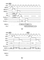
後に説明する図6(a)に示すように、図1に示したタイミング制御回路41は、リード動作を行う場合、まずカラムスイッチイネーブル信号CYEを活性化し、その後リードイネーブル信号RAEを活性化するよう構成される。カラムスイッチイネーブル信号CYEが活性化してからリードイネーブル信号RAEが活性化するまでの間、センスアンプ70により、メインIO線対MIOT_1,MIOB_1間の電位差がSAP−SANまで増幅される。その後、リードイネーブル信号RAEが活性化されると、この電位差がリードアンプ34RによってさらにVPERI−VSSまで増幅され、リードライトバスRWBS_0にはVPERI又はVSSが供給されることとなる。
As shown in FIG. 6A described later, when performing the read operation, the
以上、リード動作及びライト動作に関わる各回路の具体的な構成について、詳しく説明した。次に、図1に戻って、リフレッシュ制御回路40及びタイミング制御回路41の詳細を説明する。
The specific configuration of each circuit related to the read operation and the write operation has been described in detail above. Next, returning to FIG. 1, details of the
まず、リフレッシュ制御回路40は、メモリセルアレイ30のリフレッシュ動作を制御する回路である。リフレッシュ動作はワード線WLを活性化することによって行われるものであることから、リフレッシュ制御回路40は、リフレッシュコマンドIREF0に基づいてロウ制御回路31を制御するように構成される。つまり、リフレッシュ制御回路40が行う制御(第2の制御)は、ロウアクセス(行アクセス)である。具体的には、リフレッシュコマンドIREF0に基づいてリフレッシュコマンドIREF3を生成し、ロウ制御回路31に供給する。ロウ制御回路31は、リフレッシュ対象のロウアドレスを生成するリフレッシュアドレスカウンタ(不図示)を内蔵しており、リフレッシュコマンドIREF3により示されるタイミングでリフレッシュアドレスカウンタにより生成されるロウアドレスに対応するワード線WLを活性化することにより、リフレッシュ動作を行う。
First, the
また、リフレッシュ制御回路40は、リフレッシュコマンドIREF0に基づいてリフレッシュコマンドIREF1,IREF2(第3及び第4のコマンド信号)を生成し、タイミング制御回路41に供給する機能も有している。リフレッシュコマンドIREF1,IREF2は、リフレッシュを行う際にハイレベルに活性化されるコマンドである。詳しくは、タイミング制御回路41の説明に合わせて説明する。
The
タイミング制御回路41は、リード動作又はライト動作が行われる際に、カラム制御回路32及びリードライトアンプ34の動作タイミングを制御する回路である。この制御を行うために、タイミング制御回路41には、リードコマンドMREAD、ライトコマンドMWRITE、及び内部クロック信号ICLKが供給される。カラム制御回路32は上述したようにビット線BLを選択する回路であり、リードライトアンプ34も図3を参照して説明したようにビット線BLに関わる回路であるから、タイミング制御回路41が行う制御(第1の制御)は、カラムアクセス(列アクセス)である。
The
タイミング制御回路41は、リード動作に関連して、図4(a)に示すように、D型のラッチ回路60a〜60c及び遅延回路61a〜61dを有している。ラッチ回路60a〜60cそれぞれのクロック端子には、内部クロック信号ICLKが供給される。
The
リードコマンドMREADは、ラッチ回路60aの入力端子に供給される。リードコマンドMREADがハイとなっている期間に内部クロック信号ICLKのライジングエッジが到来すると、図6(a)に示すように、ラッチ回路60aの出力端子から出力されるリードコマンドMREAD_0がハイとなる。リードコマンドMREAD_0は、内部クロック信号ICLKの次のライジングエッジが到来するまでハイに維持される。
The read command MREAD is supplied to the input terminal of the
リードコマンドMREAD_0は、遅延回路61a及びラッチ回路60bに供給される。遅延回路61aは、リードコマンドMREAD_0を遅延時間Daにわたって遅延させ、カラムスイッチイネーブル信号CYEとして出力する回路である。したがって、図6(a)に示すように、カラムスイッチイネーブル信号CYEは、リードコマンドMREAD_0に比べてDaだけ遅延した信号となる。
The read command MREAD_0 is supplied to the
遅延回路61aから出力されたカラムスイッチイネーブル信号CYEは、上述したように図3に示したカラムスイッチ71に供給される他、遅延回路61b,61cにも供給される。遅延回路61b,61cは、カラムスイッチイネーブル信号CYEをそれぞれ遅延時間Db,Dcにわたって遅延させる回路である。遅延回路61b,61cの出力信号は、それぞれリードイネーブル信号RAE及びバスドライブ信号Busdrive_0となる。したがって、図6(a)に示すように、リードイネーブル信号RAE及びバスドライブ信号Busdrive_0は、リードコマンドMREAD_0に比べてそれぞれDa+Db,Da+Dcだけ遅延した信号となる。なお、遅延時間Dcは、遅延時間Dbに比べて大きい値に設定される。
The column switch enable signal CYE output from the
ラッチ回路60aからリードコマンドMREAD_0の供給を受けるラッチ回路60bの出力端子は、ラッチ回路60cの入力端子に接続される。つまり、ラッチ回路60a〜60cは直列に接続されている。その結果、ラッチ回路60cの出力端子から出力されるリードコマンドMREAD_1は、図6(a)に示すように、リードコマンドMREAD_0に比べて2クロック分遅延した信号となる。リードコマンドMREAD_1は、遅延回路61hに供給される。
The output terminal of the
遅延回路61hは、遅延時間DdにわたってリードコマンドMREAD_1を遅延させ、バスドライブ信号Busdrive_1として出力する回路である。したがって、図6(a)に示すように、バスドライブ信号Busdrive_1は、リードコマンドMREAD_1に比べてDdだけ遅延した信号となる。遅延時間Ddの具体的な値は、バスドライブ信号Busdrive_0が活性化されてからバスドライブ信号Busdrive_1が活性化されるまでの時間が、リードライトバスRWBSを通じて1つのリードデータを出力するのに必要な時間に等しくなるよう設定される。
The
遅延回路61a〜61dには、図1に示したリフレッシュ制御回路40から、上述したリフレッシュコマンドIREF1,IREF2も供給される。
The above-described refresh commands IREF1 and IREF2 are also supplied to the
リフレッシュ制御回路40は、図6(b)に示すように、リフレッシュコマンドIREF0がハイレベルに活性化される都度、リフレッシュコマンドIREF1,IREF2を活性化するように構成される。
As shown in FIG. 6B, the
ここで、リフレッシュ制御回路40は、リフレッシュコマンドIREF0の活性化周期より短い時間となるように、リフレッシュコマンドIREF1の活性化を維持する期間を制御している。これは、リフレッシュ制御が繰り返し実行されている間、リフレッシュコマンドIREF1が活性化されたままとなることを防止するためである。また、リフレッシュ制御回路40は、リフレッシュコマンドIREF1,IREF2を同時に活性化する一方、リフレッシュコマンドIREF1をリフレッシュコマンドIREF2より先に非活性に戻すようにしている。これは、リフレッシュ制御中に遅延回路61a〜61dの出力が活性化してしまうことのないようにするためである。
Here, the
リフレッシュコマンドIREF1,IREF2は、遅延回路61a〜61dのそれぞれを構成する複数のトランジスタにおいて、BTI劣化が発生することを抑制する役割を果たす。以下、詳しく説明する。
The refresh commands IREF1 and IREF2 play a role of suppressing the occurrence of BTI degradation in a plurality of transistors constituting each of the
遅延回路61dは、図5(a)に示すように、論理和回路からなる入力ゲート回路61daと、複数段のインバータ回路からなる内部回路61dbと、一方入力端にインバータ回路が設けられた否定論理和回路からなる出力ゲート回路61dcとを有して構成される。なお、図5(a)には遅延回路61dの内部構成のみを示しているが、遅延回路61a〜61cの内部構成も同様である。遅延時間の違いは、内部回路61dbを構成するインバータ回路の段数の違いによって実現される。以下、遅延回路61dに着目して説明する。
As shown in FIG. 5A, the
入力ゲート回路61daには、リードコマンドMREAD_1と、リフレッシュコマンドIREF1とが供給される。したがって、入力ゲート回路61daは、リードコマンドMREAD(第1のコマンド信号)及びリフレッシュコマンドIREF0(第2のコマンド信号)のいずれかが活性化されている場合(ハイレベルになっている場合)と、リードコマンドMREAD及びリフレッシュコマンドIREF0のいずれもが活性化されていない場合(ローレベルとなっている場合)とで、異なる論理状態を出力する。具体的には、前者の場合にはハイレベルを出力し、後者の場合にはローレベルを出力する。入力ゲート回路61daから出力される信号(第2の信号)は、内部回路61dbの初段を構成するインバータ回路の入力端に供給される。 A read command MREAD_1 and a refresh command IREF1 are supplied to the input gate circuit 61da. Accordingly, the input gate circuit 61da has a case where either the read command MREAD (first command signal) or the refresh command IREF0 (second command signal) is activated (when it is at a high level), Different logic states are output when both the read command MREAD and the refresh command IREF0 are not activated (when they are at a low level). Specifically, a high level is output in the former case, and a low level is output in the latter case. A signal (second signal) output from the input gate circuit 61da is supplied to the input terminal of the inverter circuit constituting the first stage of the internal circuit 61db.
内部回路61dbは、入力ゲート回路61daの出力信号の論理状態に応じて異なる動作状態となるよう構成される。具体的には、入力ゲート回路61daの出力信号がハイレベルになっている場合、奇数段目のインバータ回路の出力がローレベルとなり、偶数段目のインバータ回路の出力がハイレベルとなる(第1の動作状態)。本実施の形態による内部回路61dbは、図5(a)に示すように8段のインバータ回路を有しているので、この場合の内部回路61dbの出力ノードNODE_Aの電位レベルは、図6(b)に示すようにハイレベルとなる(期間S1)。一方、入力ゲート回路61daの出力信号がローレベルになっている場合、奇数段目のインバータ回路の出力がハイレベルとなり、偶数段目のインバータ回路の出力がローレベルとなる(第2の動作状態)。この場合の出力ノードNODE_Aの電位レベルは、図6(b)に示すようにローレベルとなる(期間S2)。 The internal circuit 61db is configured to have different operation states depending on the logic state of the output signal of the input gate circuit 61da. Specifically, when the output signal of the input gate circuit 61da is at the high level, the output of the odd-numbered inverter circuit is at the low level, and the output of the even-numbered inverter circuit is at the high level (first level). Operating state). Since the internal circuit 61db according to the present embodiment has an 8-stage inverter circuit as shown in FIG. 5A, the potential level of the output node NODE_A of the internal circuit 61db in this case is as shown in FIG. ) As shown in (). On the other hand, when the output signal of the input gate circuit 61da is at the low level, the output of the odd-numbered inverter circuit is at the high level, and the output of the even-numbered inverter circuit is at the low level (second operation state). ). In this case, the potential level of the output node NODE_A becomes a low level as shown in FIG. 6B (period S2).
ここで、内部回路61dbを構成する複数段のインバータ回路はそれぞれ、図5(b)に示すように、高位側電源配線と低位側電源配線との間にPチャンネル型MOSトランジスタ及びNチャンネル型MOSトランジスタが直列に接続された構造を有するCMOSによって構成される。内部回路61dbが上述した第1の動作状態にある場合、奇数段目のインバータ回路では、Pチャンネル型MOSトランジスタがオフ、Nチャンネル型MOSトランジスタがオンの状態となり、偶数段目のインバータ回路では、Pチャンネル型MOSトランジスタがオン、Nチャンネル型MOSトランジスタがオフの状態となる。一方、内部回路61dbが上述した第2の動作状態にある場合には、奇数段目のインバータ回路では、Pチャンネル型MOSトランジスタがオン、Nチャンネル型MOSトランジスタがオフの状態となり、偶数段目のインバータ回路では、Pチャンネル型MOSトランジスタがオフ、Nチャンネル型MOSトランジスタがオンの状態となる。 Here, as shown in FIG. 5B, each of the plural stages of inverter circuits constituting the internal circuit 61db has a P-channel MOS transistor and an N-channel MOS transistor between the high-order power supply wiring and the low-order power supply wiring. It is constituted by a CMOS having a structure in which transistors are connected in series. When the internal circuit 61db is in the first operation state described above, in the odd-numbered inverter circuit, the P-channel MOS transistor is turned off and the N-channel MOS transistor is turned on. In the even-numbered inverter circuit, The P-channel MOS transistor is turned on and the N-channel MOS transistor is turned off. On the other hand, when the internal circuit 61db is in the second operation state described above, in the odd-numbered inverter circuit, the P-channel MOS transistor is on and the N-channel MOS transistor is off, In the inverter circuit, the P-channel MOS transistor is turned off and the N-channel MOS transistor is turned on.
これらのことから理解されるように、内部回路61dbの動作状態が固定されていると、内部回路61dbを構成する複数のトランジスタのオンオフ状態も固定される。したがって、第1及び第2の動作状態のいずれであれ、内部回路61dbの動作状態が固定されている状態が長時間にわたって継続すると、内部回路61dbを構成する複数のトランジスタにBTI劣化が発生する。 As understood from these, when the operation state of the internal circuit 61db is fixed, the on / off states of the plurality of transistors constituting the internal circuit 61db are also fixed. Therefore, if the operation state of the internal circuit 61db is fixed for a long time in any of the first and second operation states, BTI degradation occurs in the plurality of transistors constituting the internal circuit 61db.
仮にリフレッシュコマンドIREF1をローレベルに固定したとすると、内部回路61dbの動作状態は、リード動作が行われない間(リードコマンドMREAD_1がローレベルとなっている間)、第2の動作状態に固定される。したがって、内部回路61dbを構成する複数のトランジスタに、BTI劣化が発生するおそれがある。しかし、本実施の形態による半導体装置10では、リフレッシュコマンドIREF0が活性化される都度、リフレッシュコマンドIREF0の活性化周期より短い時間にわたってリフレッシュコマンドIREF1をハイレベルに活性化しているので、リード動作が行われない期間であっても、リフレッシュコマンドIREF0が活性化される都度、内部回路61dbの動作状態は、第1の動作状態と第2の動作状態の間を行き来することになる。その結果、リード動作が行われないことによって内部回路61dbの動作状態が固定されてしまうことが防止されており、したがって、本実施の形態による半導体装置10によれば、内部回路61db内の複数のトランジスタにおけるBTI劣化の発生を抑制することが可能になっている。
If the refresh command IREF1 is fixed at the low level, the operation state of the internal circuit 61db is fixed to the second operation state while the read operation is not performed (while the read command MREAD_1 is at the low level). The Therefore, there is a possibility that BTI degradation occurs in the plurality of transistors constituting the internal circuit 61db. However, in the
ところで、リフレッシュコマンドIREF1の活性化に応じて内部回路61dbの動作状態が第1の動作状態に遷移した場合、内部回路61dbの出力信号は、リード動作を行わない場面であるにも関わらず、リード動作時と同様に活性化されてしまう。これがバストライブ信号Busdrive_1としてリードライトアンプ34(図1)に出力されてしまうと、誤動作の原因となる。出力ゲート回路61dcは、この誤動作を防止するために設けられている。 By the way, when the operation state of the internal circuit 61db transitions to the first operation state in response to the activation of the refresh command IREF1, the output signal of the internal circuit 61db is read even though the read operation is not performed. It is activated in the same way as during operation. If this is output to the read / write amplifier 34 (FIG. 1) as the bust live signal Busdrive_1, it causes a malfunction. The output gate circuit 61dc is provided to prevent this malfunction.
具体的に説明すると、出力ゲート回路61dcの一方入力端(インバータ回路が設けられている端部)には内部回路61dbの出力信号(第1の信号)が供給され、他方入力端(インバータ回路が設けられていない端部)にはリフレッシュコマンドIREF2が供給される。したがって、バストライブ信号Busdrive_1として内部回路61dbの出力信号が出力されるのは、リフレッシュコマンドIREF2が非活性状態(ローレベル)になっている場合のみであり、リフレッシュコマンドIREF2が活性状態(ハイレベル)となっている場合の出力ゲート回路61dcの出力は、ローレベルに固定される。 More specifically, the output signal (first signal) of the internal circuit 61db is supplied to one input terminal (an end where the inverter circuit is provided) of the output gate circuit 61dc, and the other input terminal (the inverter circuit is connected). The refresh command IREF2 is supplied to the end portion which is not provided. Therefore, the output signal of the internal circuit 61db is output as the bust signal Busbus_1 only when the refresh command IREF2 is in an inactive state (low level), and the refresh command IREF2 is in an active state (high level). In this case, the output of the output gate circuit 61dc is fixed at a low level.
ここで、上述したように、リフレッシュ制御回路40は、リフレッシュコマンドIREF1,IREF2を同時に活性化する一方、リフレッシュコマンドIREF1をリフレッシュコマンドIREF2より先に非活性に戻すようにしている。その結果として、リフレッシュコマンドIREF2は、リフレッシュコマンドIREF1の活性化に応じて内部回路61dbから出力される信号が出力ゲート回路61dcの一方入力端に到達する時点で、必ず活性化されている。したがって、半導体装置10では、リフレッシュコマンドIREF1の活性化に応じてバストライブ信号Busdrive_1がリード動作時と同様に活性化されてしまうことが防止されていると言える。
Here, as described above, the
以上説明したように、本実施の形態による半導体装置10によれば、リードコマンドMREADが非活性状態に固定されている場合であっても、リフレッシュコマンドIREF0が生成されているときには、遅延回路61a〜61d内の複数のトランジスタを、リードコマンドMREADが生成されている場合と同じ第1の動作状態とすることが可能になる。また、遅延回路61a〜61dは、リフレッシュコマンドIREF0に対応して内部の複数のトランジスタが第1の動作状態となるように構成されているので、第1の動作状態が長時間にわたって維持されることもない。さらに、リフレッシュコマンドIREF0に対応して遅延回路61a〜61d内の複数のトランジスタを第1の動作状態としているにも関わらず、タイミング制御回路41の出力信号CYE,RAE,Busdrive_0,Busdrive_1がリード動作時と同様に活性化されてしまうこともない。したがって、本実施の形態による半導体装置10によれば、遅延回路61a〜61d内の複数のトランジスタにおけるBTI劣化の発生を、好適に抑制することが可能になる。
As described above, according to the
また、本実施の形態による半導体装置10では、遅延回路61a〜61d内の複数のトランジスタを第1の動作状態とするためのコマンドとしてリフレッシュコマンドIREF0を用いているが、上述したようにリフレッシュコマンドIREF0は定期的に活性化されるものである。したがって、本実施の形態による半導体装置10によれば、他のコマンドを利用する場合に比べ、遅延回路61a〜61d内の複数のトランジスタのBTI劣化を確実に緩和できる、という効果も奏される。
In the
ここまで、タイミング制御回路41内の回路のうちリード動作に関連する部分に着目して説明したが、ライト動作に関連する部分についても、同様の構成によりBTI劣化の発生を抑制できる。以下、詳しく説明する。
Up to this point, the description has been given focusing on the portion related to the read operation in the circuit in the
タイミング制御回路41は、ライト動作に関連して、図4(b)に示すように、D型のラッチ回路60d〜60f及び遅延回路61e〜61hを有している。ラッチ回路60d〜60fそれぞれのクロック端子には、内部クロック信号ICLKが供給される。
The
ライトコマンドMWRITEは、ラッチ回路60dの入力端子に供給される。ラッチ回路60dは、内部クロック信号ICLKのライジングエッジでライトコマンドMWRITEをラッチし、ライトコマンドMWRITE_0として出力する回路である。出力されたライトコマンドMWRITE_0は、遅延回路61e及びラッチ回路60eに供給される。
The write command MWRITE is supplied to the input terminal of the
遅延回路61eは、ライトコマンドMWRITE_0を遅延時間Deにわたって遅延させ、バスドライブ信号Busdrive_0として出力する回路である。一方、ラッチ回路60a〜60cは直列に接続されており、したがって、ラッチ回路60cから出力されるライトコマンドMWRITE_1は、ライトコマンドMWRITE_0に比べて2クロック分遅延した信号となる。ライトコマンドMWRITE_1は、遅延回路61f〜61hのそれぞれに供給される。
The
遅延回路61f〜61hはそれぞれ、ライトコマンドMWRITE_1を遅延時間Df,Dg,Dhにわたって遅延させる回路である。遅延回路61f〜61hの出力信号は、それぞれライトイネーブル信号WAE、カラムスイッチイネーブル信号CYE、バスドライブ信号Busdrive_1となる。
The
リード動作に関する遅延回路61a〜61dと同じく、遅延回路61e〜61hにもリフレッシュコマンドIREF1,IREF2が供給される。遅延回路61e〜61hの内部構成は、図5(a)に示した遅延回路61dのものと同様である。したがって、遅延回路61e〜61hにおいても、遅延回路61a〜61dと同様、内部回路を構成する複数のトランジスタにおけるBTI劣化の発生が、好適に抑制される。
Similarly to the
次に、図7を参照しながら、本発明の第2の実施の形態による半導体装置について説明する。 Next, a semiconductor device according to a second embodiment of the present invention will be described with reference to FIG.
第1の実施の形態による半導体装置10では1本のリードライトバスRWBSに2台のリードライトアンプ34が接続されていた(図2を参照)が、本実施の形態による半導体装置では、1本のリードライトバスRWBSに1台のリードライトアンプ34が接続される。したがって、本実施の形態による半導体装置は、8×N本のリードライトバスRWBSを有して構成される。また、これによりリードライトバスRWBSに接続されるリードライトアンプ34を切り替える必要がなくなることから、バスドライブ信号Busdrive_0,Busdrive_1に代えて、図7に示すように、単一のバスドライブ信号Busdriveを用いるように構成される。その他の点では第1の実施の形態による半導体装置10と同一であるので、以下、相違点に着目して説明する。
In the
単一のバスドライブ信号Busdriveを用いるため、本実施の形態によるタイミング制御回路41は、図7に示すように、図4に示したタイミング制御回路41とは異なり、バスドライブ信号Busdrive_1を生成するための構成(ラッチ回路60b,60c及び遅延回路61d)を有しない。その他の点では図4に示したタイミング制御回路41と同様であり、遅延回路61a〜61cから、それぞれカラムスイッチイネーブル信号CYE、リードイネーブル信号RAE、バスドライブ信号Busdriveが出力される。
Since the single bus drive signal Busdrive is used, the
本実施の形態による遅延回路61a〜61cにも、第1の実施の形態による遅延回路61a〜61cと同様、リフレッシュコマンドIREF1,IREF2が供給される。したがって、本実施の形態による半導体装置においても、遅延回路61a〜61c内の複数のトランジスタにおけるBTI劣化の発生を、好適に抑制することが実現されている。
Similarly to the
次に、図8を参照しながら、本発明の第3の実施の形態による半導体装置について説明する。 Next, a semiconductor device according to a third embodiment of the present invention will be described with reference to FIG.
本実施の形態による半導体装置は、図8に示す遅延回路80を備えて構成される。遅延回路80は、図8に示すように、論理和回路からなる入力ゲート回路80aと、複数段のインバータ回路からなる内部回路80bと、一方入力端にインバータ回路が設けられた否定論理和回路からなる出力ゲート回路80cとを有して構成される。図5を参照すると理解されるように、この構成は上述した遅延回路61a〜61hのものと同様である。
The semiconductor device according to the present embodiment includes a
図示していないが、本実施の形態による半導体装置は、制御信号ICOM1(第1のコマンド信号)に基づく制御(第1の制御)と、制御信号ICOM2(第2のコマンド信号)に基づく制御(第2の制御)とを行うように構成される。入力ゲート回路80aの一方入力端には制御信号ICOM1が供給されており、入力ゲート回路80aの出力信号は内部回路80bに供給され、内部回路80bの出力信号は出力ゲート回路80cの一方入力端(インバータ回路が設けられている端部)に供給される。これにより、遅延回路80は、制御信号ICOM1を遅延させてなる遅延信号ICOM1_delayを出力するように構成される。
Although not shown, the semiconductor device according to the present embodiment has a control based on the control signal ICOM1 (first command signal) (first control) and a control based on the control signal ICOM2 (second command signal) ( (Second control). The control signal ICOM1 is supplied to one input terminal of the
入力ゲート回路80aの他方入力端には、制御信号ICOM2_en(第3のコマンド信号)が供給される。また、出力ゲート回路80cの他方入力端(インバータ回路が設けられていない端部)には制御信号ICOM2_mask(第4のコマンド信号)が供給される。制御信号ICOM2_enは、制御信号ICOM2の活性化に応じてハイレベルに活性化される信号であり、制御信号ICOM2_enは、制御信号ICOM2が活性化している間に遅延信号ICOM1_delayが活性化されないよう、出力ゲート回路80cの出力を固定する役割を担う信号である。
A control signal ICOM2_en (third command signal) is supplied to the other input terminal of the
以上の構成により、本実施の形態による半導体装置によれば、制御信号ICOM1が非活性状態に固定されている場合であっても、制御信号ICOM2が生成されているときには、遅延回路80内の複数のトランジスタ(具体的には、内部回路80b内の各インバータ回路を構成するトランジスタ)を、制御信号ICOM1が生成されている場合と同じ動作状態(第1の動作状態)とすることが可能になる。また、遅延回路80は、制御信号ICOM2に対応して内部の複数のトランジスタが第1の動作状態となるように構成されているので、第1の動作状態が長時間にわたって維持されることもない。さらに、制御信号ICOM2に対応して遅延回路80内の複数のトランジスタを第1の動作状態としているにも関わらず、遅延信号ICOM1_delayが制御信号ICOM1の活性化時と同様に活性化されてしまうこともない。したがって、本実施の形態による半導体装置によれば、遅延回路80内の複数のトランジスタにおけるBTI劣化の発生を、好適に抑制することが可能になる。
With the above configuration, according to the semiconductor device according to the present embodiment, even when the control signal ICOM1 is fixed to the inactive state, when the control signal ICOM2 is generated, a plurality of delay signals in the
なお、本実施の形態による遅延回路80は、第1及び第2の実施の形態で説明した遅延回路61a〜61hとして用いることが可能である。この場合、制御信号ICOM1はリードコマンドMREAD又はライトコマンドMWRITEとなり、制御信号ICOM2_en,ICOM2_maskはそれぞれ、リフレッシュコマンドIREF1,IREF2となる。その他の用途で遅延回路80を用いることも、もちろん可能である。
The
以上、本発明の好ましい実施形態について説明したが、本発明は、上記の実施形態に限定されることなく、本発明の主旨を逸脱しない範囲で種々の変更が可能であり、それらも本発明の範囲内に包含されるものであることはいうまでもない。 The preferred embodiments of the present invention have been described above, but the present invention is not limited to the above-described embodiments, and various modifications can be made without departing from the spirit of the present invention. Needless to say, it is included in the range.
例えば、上述した第1乃至第3の実施の形態では、BTI劣化発生の防止対象である内部回路として遅延回路内の複数段のインバータ回路を取り上げたが、本発明は、遅延回路内の複数段のインバータ回路でなくても、BTI劣化が発生する可能性のあるトランジスタを含む回路に広く適用可能である。 For example, in the first to third embodiments described above, a plurality of stages of inverter circuits in the delay circuit are taken up as the internal circuit that is the target of preventing the occurrence of BTI degradation. However, the present invention provides a plurality of stages in the delay circuit. Even if it is not an inverter circuit, it can be widely applied to a circuit including a transistor in which BTI degradation may occur.
また、本発明は、SRAM(Static Random Access Memory)などの揮発性メモリや、フラッシュメモリ、PRAM(Phase change Random Access Memory)、ReRAM(Resistance Random Access Memory)、STT−RAM(Spin Transfer Torque Random Access Memory)などの不揮発性メモリなど、コマンド制御を受ける半導体装置に広く適用可能である。さらに、本発明は、コマンドを発行する装置であるコントローラにも適用可能である。 The present invention also provides a volatile memory such as SRAM (Static Random Access Memory), flash memory, PRAM (Phase change Random Access Memory), ReRAM (Resistance Random Access Memory), STT-RAM (Spin Transfer Torque Random Access Memory). It can be widely applied to semiconductor devices that are subject to command control, such as non-volatile memories. Furthermore, the present invention is also applicable to a controller that is a device that issues a command.
10 半導体装置
11a,11b クロック端子
12 コマンド端子
13 アドレス端子
14 データ入出力端子
15a,15b,16 電源端子
20 クロック入力回路
21 DLL回路
22 タイミングジェネレーター
23 コマンド入力回路
24 コマンドデコード回路
25 アドレス入力回路
26 アドレスラッチ回路
30 メモリセルアレイ
31 ロウ制御回路
32 カラム制御回路
33 データ入出力回路
34 リードライトアンプ
34C 接続回路
34R リードアンプ
34W ライトアンプ
35 入出力回路
35a FIFO
35b 入出力バッファ
40 リフレッシュ制御回路
41 タイミング制御回路
50 内部電源発生回路
60a〜60f ラッチ回路
61a〜61h 遅延回路
61da,80a 入力ゲート回路
61db,80b 内部回路
61dc,80c 出力ゲート回路
70 センスアンプ
71 カラムスイッチ
72 プリチャージ回路
73 IOスイッチ
80 遅延回路
BL,BLT,BLB ビット線
MIOT,MIOB メインIO線
MC メモリセル
OUTBS 内部バス
RWBS リードライトバス
WL ワード線
DESCRIPTION OF
35b Input /
Claims (10)
複数のトランジスタを含み、前記コマンド生成回路が前記第1及び第2のコマンド信号のいずれか少なくとも一方を活性化していることに対応して、該複数のトランジスタが第1の動作状態となるよう構成された内部回路と、
前記内部回路から出力される第1の信号を受け、前記コマンド生成回路が前記第2のコマンド信号を活性化していないことに対応して該第1の信号を出力する一方、前記コマンド生成回路が前記第2のコマンド信号を活性化していることに対応して該第1の信号を出力しないよう構成された出力ゲート回路と
を備えることを特徴とする半導体装置。 A command generation circuit for activating the first and second command signals;
A plurality of transistors, wherein the plurality of transistors are in a first operating state in response to the command generation circuit activating at least one of the first and second command signals. Internal circuit,
In response to the first signal output from the internal circuit, the command generation circuit outputs the first signal in response to the command generation circuit not activating the second command signal, while the command generation circuit An output gate circuit configured not to output the first signal in response to activation of the second command signal.
ことを特徴とする請求項1に記載の半導体装置。 In response to the command generation circuit not activating the first and second command signals, the internal circuit causes the plurality of transistors to enter a second operation state different from the first operation state. The semiconductor device according to claim 1, wherein the semiconductor device is configured as follows.
第2の制御回路とを備え、
前記第1の制御回路は、前記コマンド生成回路が前記第1のコマンド信号を活性化していることに対応して前記出力ゲート回路から前記第1の信号を出力することにより第1の制御を行う一方、前記コマンド生成回路が前記第2のコマンド信号を活性化していることに対応して該第1の制御を行わないよう構成され、
前記第2の制御回路は、前記コマンド生成回路が前記第2のコマンド信号を活性化していることに対応して、前記第1の制御とは異なる第2の制御を行うよう構成される
ことを特徴とする請求項1又は2に記載の半導体装置。 A first control circuit including the internal circuit and the output gate circuit;
A second control circuit,
The first control circuit performs the first control by outputting the first signal from the output gate circuit in response to the command generation circuit activating the first command signal. On the other hand, the command generation circuit is configured not to perform the first control in response to the activation of the second command signal,
The second control circuit is configured to perform a second control different from the first control in response to the command generation circuit activating the second command signal. The semiconductor device according to claim 1, wherein the semiconductor device is characterized.
前記内部回路は、前記第1及び第3のコマンド信号のいずれか少なくとも一方が活性化された場合に、前記複数のトランジスタが第1の動作状態となるよう構成される
ことを特徴とする請求項3に記載の半導体装置。 The second control circuit is configured to activate a third command signal in response to the activation of the second command signal;
The internal circuit is configured such that when at least one of the first and third command signals is activated, the plurality of transistors are in a first operation state. 3. The semiconductor device according to 3.
前記第2の制御回路は、前記第2のコマンド信号が活性化される都度、前記第3のコマンド信号を活性化するよう構成され、
前記第3のコマンド信号の活性化が継続する期間は、前記第2のコマンド信号の活性化周期より短い
ことを特徴とする請求項4に記載の半導体装置。 The second command signal is a signal that is periodically activated;
The second control circuit is configured to activate the third command signal each time the second command signal is activated,
The semiconductor device according to claim 4, wherein a period during which the activation of the third command signal continues is shorter than an activation cycle of the second command signal.
前記入力ゲート回路から出力される第2の信号は、前記複数段のインバータ回路の初段を構成する前記インバータ回路の入力端に供給される
ことを特徴とする請求項4又は5に記載の半導体装置。 A different logic state is output when at least one of the first and third command signals is activated and when both of the first and third command signals are not activated. An input gate circuit;
6. The semiconductor device according to claim 4, wherein the second signal output from the input gate circuit is supplied to an input terminal of the inverter circuit constituting the first stage of the plurality of inverter circuits. .
前記第4のコマンド信号が活性化されている場合の前記出力ゲート回路の出力は、一定値に固定される
ことを特徴とする請求項3乃至6のいずれか一項に記載の半導体装置。 The second control circuit is configured to activate a fourth command signal in response to the activation of the second command signal;
7. The semiconductor device according to claim 3, wherein an output of the output gate circuit when the fourth command signal is activated is fixed to a constant value. 8.
前記第1の制御は前記列アクセスであり、
前記第2の制御は前記行アクセスである
ことを特徴とする請求項3乃至7のいずれか一項に記載の半導体装置。 A plurality of memory cells arranged in a matrix and selected by row access and column access;
The first control is the column access;
The semiconductor device according to claim 3, wherein the second control is the row access.
前記第2の制御は、前記複数のメモリセルに対するリフレッシュ制御である
ことを特徴とする請求項8に記載の半導体装置。 The first control is read control or write control for the plurality of memory cells,
The semiconductor device according to claim 8, wherein the second control is refresh control for the plurality of memory cells.
前記複数のトランジスタは、前記複数段のインバータ回路を構成する
ことを特徴とする請求項1乃至9のいずれか一項に記載の半導体装置。 The internal circuit is configured to include a plurality of inverter circuits,
The semiconductor device according to claim 1, wherein the plurality of transistors constitute the plurality of stages of inverter circuits.
Priority Applications (4)
| Application Number | Priority Date | Filing Date | Title |
|---|---|---|---|
| JP2013133557A JP2015008029A (en) | 2013-06-26 | 2013-06-26 | Semiconductor device |
| US14/315,951 US9424907B2 (en) | 2013-06-26 | 2014-06-26 | Semiconductor device suppressing BTI deterioration |
| US15/236,281 US9728246B2 (en) | 2013-06-26 | 2016-08-12 | Semiconductor device suppressing BTI deterioration |
| US15/641,118 US10242729B2 (en) | 2013-06-26 | 2017-07-03 | Semiconductor device suppressing BTI deterioration |
Applications Claiming Priority (1)
| Application Number | Priority Date | Filing Date | Title |
|---|---|---|---|
| JP2013133557A JP2015008029A (en) | 2013-06-26 | 2013-06-26 | Semiconductor device |
Publications (1)
| Publication Number | Publication Date |
|---|---|
| JP2015008029A true JP2015008029A (en) | 2015-01-15 |
Family
ID=52115473
Family Applications (1)
| Application Number | Title | Priority Date | Filing Date |
|---|---|---|---|
| JP2013133557A Pending JP2015008029A (en) | 2013-06-26 | 2013-06-26 | Semiconductor device |
Country Status (2)
| Country | Link |
|---|---|
| US (3) | US9424907B2 (en) |
| JP (1) | JP2015008029A (en) |
Families Citing this family (48)
| Publication number | Priority date | Publication date | Assignee | Title |
|---|---|---|---|---|
| US9324398B2 (en) | 2013-02-04 | 2016-04-26 | Micron Technology, Inc. | Apparatuses and methods for targeted refreshing of memory |
| JP2015008029A (en) | 2013-06-26 | 2015-01-15 | マイクロン テクノロジー, インク. | Semiconductor device |
| US9047978B2 (en) | 2013-08-26 | 2015-06-02 | Micron Technology, Inc. | Apparatuses and methods for selective row refreshes |
| JP2015219938A (en) | 2014-05-21 | 2015-12-07 | マイクロン テクノロジー, インク. | Semiconductor device |
| JP2017182854A (en) | 2016-03-31 | 2017-10-05 | マイクロン テクノロジー, インク. | Semiconductor device |
| KR102521756B1 (en) | 2016-06-22 | 2023-04-14 | 삼성전자주식회사 | Delay circuit of semiconductor memory device, semiconductor memory device and method of operating the same |
| US10083736B1 (en) * | 2016-06-23 | 2018-09-25 | Apple Inc. | Adaptive calibration scheduling for a memory subsystem based on calibrations of delay applied to data strobe and calibration of reference voltage |
| US10490251B2 (en) | 2017-01-30 | 2019-11-26 | Micron Technology, Inc. | Apparatuses and methods for distributing row hammer refresh events across a memory device |
| US10580475B2 (en) | 2018-01-22 | 2020-03-03 | Micron Technology, Inc. | Apparatuses and methods for calculating row hammer refresh addresses in a semiconductor device |
| US11017833B2 (en) | 2018-05-24 | 2021-05-25 | Micron Technology, Inc. | Apparatuses and methods for pure-time, self adopt sampling for row hammer refresh sampling |
| US11152050B2 (en) | 2018-06-19 | 2021-10-19 | Micron Technology, Inc. | Apparatuses and methods for multiple row hammer refresh address sequences |
| US10685696B2 (en) | 2018-10-31 | 2020-06-16 | Micron Technology, Inc. | Apparatuses and methods for access based refresh timing |
| WO2020117686A1 (en) | 2018-12-03 | 2020-06-11 | Micron Technology, Inc. | Semiconductor device performing row hammer refresh operation |
| CN117198356A (en) | 2018-12-21 | 2023-12-08 | 美光科技公司 | Apparatus and method for timing interleaving for targeted refresh operations |
| US10957377B2 (en) | 2018-12-26 | 2021-03-23 | Micron Technology, Inc. | Apparatuses and methods for distributed targeted refresh operations |
| US10770127B2 (en) | 2019-02-06 | 2020-09-08 | Micron Technology, Inc. | Apparatuses and methods for managing row access counts |
| US11226752B2 (en) | 2019-03-05 | 2022-01-18 | Apple Inc. | Filtering memory calibration |
| US11043254B2 (en) | 2019-03-19 | 2021-06-22 | Micron Technology, Inc. | Semiconductor device having cam that stores address signals |
| US11227649B2 (en) | 2019-04-04 | 2022-01-18 | Micron Technology, Inc. | Apparatuses and methods for staggered timing of targeted refresh operations |
| US11264096B2 (en) | 2019-05-14 | 2022-03-01 | Micron Technology, Inc. | Apparatuses, systems, and methods for a content addressable memory cell with latch and comparator circuits |
| US11158364B2 (en) | 2019-05-31 | 2021-10-26 | Micron Technology, Inc. | Apparatuses and methods for tracking victim rows |
| US11069393B2 (en) | 2019-06-04 | 2021-07-20 | Micron Technology, Inc. | Apparatuses and methods for controlling steal rates |
| US11158373B2 (en) | 2019-06-11 | 2021-10-26 | Micron Technology, Inc. | Apparatuses, systems, and methods for determining extremum numerical values |
| US10832792B1 (en) | 2019-07-01 | 2020-11-10 | Micron Technology, Inc. | Apparatuses and methods for adjusting victim data |
| US11139015B2 (en) | 2019-07-01 | 2021-10-05 | Micron Technology, Inc. | Apparatuses and methods for monitoring word line accesses |
| US11386946B2 (en) | 2019-07-16 | 2022-07-12 | Micron Technology, Inc. | Apparatuses and methods for tracking row accesses |
| US10943636B1 (en) | 2019-08-20 | 2021-03-09 | Micron Technology, Inc. | Apparatuses and methods for analog row access tracking |
| US10964378B2 (en) | 2019-08-22 | 2021-03-30 | Micron Technology, Inc. | Apparatus and method including analog accumulator for determining row access rate and target row address used for refresh operation |
| US11200942B2 (en) | 2019-08-23 | 2021-12-14 | Micron Technology, Inc. | Apparatuses and methods for lossy row access counting |
| US11302374B2 (en) | 2019-08-23 | 2022-04-12 | Micron Technology, Inc. | Apparatuses and methods for dynamic refresh allocation |
| US11302377B2 (en) | 2019-10-16 | 2022-04-12 | Micron Technology, Inc. | Apparatuses and methods for dynamic targeted refresh steals |
| US11309010B2 (en) | 2020-08-14 | 2022-04-19 | Micron Technology, Inc. | Apparatuses, systems, and methods for memory directed access pause |
| US11348631B2 (en) | 2020-08-19 | 2022-05-31 | Micron Technology, Inc. | Apparatuses, systems, and methods for identifying victim rows in a memory device which cannot be simultaneously refreshed |
| US11380382B2 (en) | 2020-08-19 | 2022-07-05 | Micron Technology, Inc. | Refresh logic circuit layout having aggressor detector circuit sampling circuit and row hammer refresh control circuit |
| US11222682B1 (en) | 2020-08-31 | 2022-01-11 | Micron Technology, Inc. | Apparatuses and methods for providing refresh addresses |
| US11557331B2 (en) | 2020-09-23 | 2023-01-17 | Micron Technology, Inc. | Apparatuses and methods for controlling refresh operations |
| US11222686B1 (en) | 2020-11-12 | 2022-01-11 | Micron Technology, Inc. | Apparatuses and methods for controlling refresh timing |
| US11462291B2 (en) | 2020-11-23 | 2022-10-04 | Micron Technology, Inc. | Apparatuses and methods for tracking word line accesses |
| WO2022132475A1 (en) | 2020-12-17 | 2022-06-23 | Micron Technology, Inc. | Memory activation timing management |
| WO2022132476A1 (en) | 2020-12-17 | 2022-06-23 | Micron Technology, Inc. | Memory activation timing management |
| US11264079B1 (en) | 2020-12-18 | 2022-03-01 | Micron Technology, Inc. | Apparatuses and methods for row hammer based cache lockdown |
| US11482275B2 (en) | 2021-01-20 | 2022-10-25 | Micron Technology, Inc. | Apparatuses and methods for dynamically allocated aggressor detection |
| US11600314B2 (en) | 2021-03-15 | 2023-03-07 | Micron Technology, Inc. | Apparatuses and methods for sketch circuits for refresh binning |
| US11664063B2 (en) | 2021-08-12 | 2023-05-30 | Micron Technology, Inc. | Apparatuses and methods for countering memory attacks |
| US11688451B2 (en) | 2021-11-29 | 2023-06-27 | Micron Technology, Inc. | Apparatuses, systems, and methods for main sketch and slim sketch circuit for row address tracking |
| US12165687B2 (en) | 2021-12-29 | 2024-12-10 | Micron Technology, Inc. | Apparatuses and methods for row hammer counter mat |
| US12125514B2 (en) | 2022-04-28 | 2024-10-22 | Micron Technology, Inc. | Apparatuses and methods for access based refresh operations |
| US12112787B2 (en) | 2022-04-28 | 2024-10-08 | Micron Technology, Inc. | Apparatuses and methods for access based targeted refresh operations |
Family Cites Families (13)
| Publication number | Priority date | Publication date | Assignee | Title |
|---|---|---|---|---|
| KR100450682B1 (en) * | 2002-08-29 | 2004-10-01 | 삼성전자주식회사 | A semiconductor memory device having internal circuits for improving test efficiency and the test method thereof |
| JP4111789B2 (en) * | 2002-09-13 | 2008-07-02 | 富士通株式会社 | Semiconductor memory device control method and semiconductor memory device |
| US7200050B2 (en) * | 2003-05-26 | 2007-04-03 | Semiconductor Energy Laboratory Co., Ltd. | Memory unit and semiconductor device |
| JP4768221B2 (en) * | 2003-11-07 | 2011-09-07 | 富士通セミコンダクター株式会社 | Memory device |
| JP2007323770A (en) | 2006-06-02 | 2007-12-13 | Renesas Technology Corp | Sram |
| US7859920B2 (en) * | 2008-03-14 | 2010-12-28 | Qualcomm Incorporated | Advanced bit line tracking in high performance memory compilers |
| KR101464255B1 (en) * | 2008-06-23 | 2014-11-25 | 삼성전자주식회사 | Flash memory device and system including the same |
| KR20110001396A (en) * | 2009-06-30 | 2011-01-06 | 삼성전자주식회사 | Semiconductor memory device can reduce power consumption |
| JP2011061457A (en) * | 2009-09-09 | 2011-03-24 | Elpida Memory Inc | Clock generating circuit, semiconductor device including the same, and data processing system |
| JP5642524B2 (en) * | 2010-12-13 | 2014-12-17 | ピーエスフォー ルクスコ エスエイアールエルPS4 Luxco S.a.r.l. | Semiconductor device |
| JP2012129851A (en) * | 2010-12-16 | 2012-07-05 | Elpida Memory Inc | Semiconductor device |
| KR101980162B1 (en) * | 2012-06-28 | 2019-08-28 | 에스케이하이닉스 주식회사 | Memrory |
| JP2015008029A (en) | 2013-06-26 | 2015-01-15 | マイクロン テクノロジー, インク. | Semiconductor device |
-
2013
- 2013-06-26 JP JP2013133557A patent/JP2015008029A/en active Pending
-
2014
- 2014-06-26 US US14/315,951 patent/US9424907B2/en active Active
-
2016
- 2016-08-12 US US15/236,281 patent/US9728246B2/en active Active
-
2017
- 2017-07-03 US US15/641,118 patent/US10242729B2/en active Active
Also Published As
| Publication number | Publication date |
|---|---|
| US20150003177A1 (en) | 2015-01-01 |
| US20160351246A1 (en) | 2016-12-01 |
| US9728246B2 (en) | 2017-08-08 |
| US9424907B2 (en) | 2016-08-23 |
| US20170301390A1 (en) | 2017-10-19 |
| US10242729B2 (en) | 2019-03-26 |
Similar Documents
| Publication | Publication Date | Title |
|---|---|---|
| US10242729B2 (en) | Semiconductor device suppressing BTI deterioration | |
| US8767497B2 (en) | Semiconductor device performing self refresh operation | |
| US10147477B2 (en) | System, method, and controller for supplying address and command signals after a chip select signal | |
| US7184362B2 (en) | Page access circuit of semiconductor memory device | |
| CN111986718B (en) | Systems, methods, and apparatus for temperature compensated operation of electronic devices | |
| US6542426B2 (en) | Cell data protection circuit in semiconductor memory device and method of driving refresh mode | |
| JP2012252733A (en) | Semiconductor device | |
| JP2011114773A (en) | Semiconductor device, method of controlling the same, and system employing the same | |
| JP5595240B2 (en) | Semiconductor device | |
| US9076503B2 (en) | Semiconductor device | |
| US9136844B2 (en) | Semiconductor device having level shifter | |
| JP2015219927A (en) | Semiconductor device | |
| US10347316B2 (en) | Input buffer circuit | |
| US8395962B2 (en) | Semiconductor memory device and method for operating the same | |
| KR100745072B1 (en) | Internal voltage discharge circuit | |
| US12537044B2 (en) | Semiconductor device and memory device including complementary delay circuits for maximizing operation efficiency while minimizing area occupied by delay circuits | |
| JP2012018711A (en) | Semiconductor device and control method thereof | |
| KR100652796B1 (en) | Semiconductor memory device | |
| JP2013093513A (en) | Semiconductor device | |
| JP2014229332A (en) | Semiconductor device | |
| KR100950578B1 (en) | Semiconductor memory device and driving method thereof | |
| JP2013037729A (en) | Semiconductor device | |
| US9070425B2 (en) | Data line control for sense amplifiers | |
| WO2014115601A1 (en) | Semiconductor device | |
| KR20110076500A (en) | Semiconductor memory device |