JP2014229711A - Semiconductor device - Google Patents
Semiconductor device Download PDFInfo
- Publication number
- JP2014229711A JP2014229711A JP2013107381A JP2013107381A JP2014229711A JP 2014229711 A JP2014229711 A JP 2014229711A JP 2013107381 A JP2013107381 A JP 2013107381A JP 2013107381 A JP2013107381 A JP 2013107381A JP 2014229711 A JP2014229711 A JP 2014229711A
- Authority
- JP
- Japan
- Prior art keywords
- electrode
- wiring
- insulating film
- metal pattern
- layer
- Prior art date
- Legal status (The legal status is an assumption and is not a legal conclusion. Google has not performed a legal analysis and makes no representation as to the accuracy of the status listed.)
- Pending
Links
Images


Landscapes
- Internal Circuitry In Semiconductor Integrated Circuit Devices (AREA)
- Semiconductor Integrated Circuits (AREA)
Abstract
【課題】容量素子を有する半導体装置の信頼性や性能を向上させる。【解決手段】半導体基板上に形成した複数の配線層のうちのいずれかの配線層に、容量素子C1の下部電極LEを設け、下部電極LEが形成された配線層よりも2つ上層の配線層において、下部電極LEの上方に容量素子C1の上部電極UEを設ける。そして、下部電極LEが形成された配線層よりも1つ上層の配線層において、下部電極LEと上部電極UEとの間に位置する浮遊電極FEを設ける。【選択図】図8The reliability and performance of a semiconductor device having a capacitor element are improved. A lower electrode LE of a capacitor element C1 is provided in any one of a plurality of wiring layers formed on a semiconductor substrate, and two wirings higher than the wiring layer in which the lower electrode LE is formed. In the layer, the upper electrode UE of the capacitive element C1 is provided above the lower electrode LE. Then, the floating electrode FE located between the lower electrode LE and the upper electrode UE is provided in the wiring layer one layer above the wiring layer in which the lower electrode LE is formed. [Selection] Figure 8
Description
本発明は、半導体装置に関し、例えば、容量素子を有する半導体装置に好適に利用できるものである。 The present invention relates to a semiconductor device, and can be suitably used for a semiconductor device having a capacitor, for example.
半導体基板上に、MISFET(Metal Insulator Semiconductor Field Effect Transistor)や容量素子などを形成し、各素子間を配線で結線することで種々の半導体装置が製造される。半導体基板上に形成される容量素子には、MIM(Metal Insulator Metal)型容量素子がある。 Various semiconductor devices are manufactured by forming MISFETs (Metal Insulator Semiconductor Field Effect Transistors), capacitive elements, and the like on a semiconductor substrate and connecting the elements with wiring. As a capacitive element formed on a semiconductor substrate, there is a MIM (Metal Insulator Metal) type capacitive element.
特開2009−33029号公報(特許文献1)には、DRAMの配線に関する技術が記載されている。 Japanese Unexamined Patent Application Publication No. 2009-33029 (Patent Document 1) describes a technique related to wiring of a DRAM.
特開2005−183739号公報(特許文献2)には、櫛型状に配列された複数の配線をもつ電極により容量素子を形成する技術が記載されている。 Japanese Patent Laying-Open No. 2005-183739 (Patent Document 2) describes a technique in which a capacitor element is formed by electrodes having a plurality of wirings arranged in a comb shape.
特開2009−224637号公報(特許文献3)には、櫛型形状の金属パターンで電極を形成したMIM型の容量素子に関する技術が記載されている。 Japanese Patent Laying-Open No. 2009-224737 (Patent Document 3) describes a technique related to an MIM type capacitive element in which electrodes are formed with a comb-shaped metal pattern.
容量素子を有する半導体装置においても、できるだけ信頼性を向上させることが望まれる。または、できるだけ性能を向上させることが望まれる。若しくは、信頼性を向上させ、かつ、性能を向上させることが望まれる。 Even in a semiconductor device having a capacitor element, it is desired to improve the reliability as much as possible. Alternatively, it is desired to improve the performance as much as possible. Alternatively, it is desirable to improve reliability and improve performance.
その他の課題と新規な特徴は、本明細書の記述および添付図面から明らかになるであろう。 Other problems and novel features will become apparent from the description of the specification and the accompanying drawings.
一実施の形態によれば、半導体基板上に形成した複数の配線層のうちのいずれかの配線層に、容量素子の第1電極を設け、前記第1電極が形成された配線層よりも2つ上層の配線層において、前記第1電極の上方に前記容量素子の第2電極を設け、前記第1電極が形成された配線層よりも1つ上層の配線層において、前記第1電極と前記第2電極との間に浮遊電極を設ける。 According to one embodiment, the first electrode of the capacitive element is provided in any one of the plurality of wiring layers formed on the semiconductor substrate, and is 2 rather than the wiring layer in which the first electrode is formed. In the upper wiring layer, the second electrode of the capacitive element is provided above the first electrode. In the wiring layer one layer higher than the wiring layer on which the first electrode is formed, the first electrode and the A floating electrode is provided between the second electrode.
また、一実施の形態によれば、半導体基板上に形成した複数の配線層のうちのいずれかの配線層に第1金属パターンおよび第2金属パターンを設け、前記第1金属パターンおよび第2金属パターンが形成された配線層よりも1つ上層の配線層に、第3金属パターンおよび第4金属パターンを設ける。前記第1金属パターンと前記第3金属パターンは、互いに電気的に接続されて容量素子の一方の電極を形成し、前記第2金属パターンと前記第4金属パターンは、互いに電気的に接続されて前記容量素子の他方の電極を形成する。前記第1金属パターンは、第1方向にそれぞれ延在する複数の第1電極部を含んでおり、前記第2金属パターンは、前記第1方向にそれぞれ延在する複数の第2電極部を含んでおり、前記第1電極部と前記第2電極部とは、前記第1方向と交差する第2方向に交互に並んでいる。前記第3金属パターンは、前記第1方向にそれぞれ延在する複数の第3電極部を含んでおり、前記第4金属パターンは、前記第1方向にそれぞれ延在する複数の第4電極部を含んでおり、前記第3電極部と前記第4電極部とは、前記第2方向に交互に並んでいる。前記複数の第1電極部のそれぞれは、平面視において、前記第2方向に隣り合う前記第3電極部と前記第4電極部との間に配置されており、前記複数の第2電極部のそれぞれは、平面視において、前記第2方向に隣り合う前記第3電極部と前記第4電極部との間に配置されている。 According to one embodiment, the first metal pattern and the second metal pattern are provided on any one of the plurality of wiring layers formed on the semiconductor substrate, and the first metal pattern and the second metal pattern are provided. A third metal pattern and a fourth metal pattern are provided in a wiring layer one layer above the wiring layer on which the pattern is formed. The first metal pattern and the third metal pattern are electrically connected to each other to form one electrode of a capacitive element, and the second metal pattern and the fourth metal pattern are electrically connected to each other. The other electrode of the capacitive element is formed. The first metal pattern includes a plurality of first electrode portions extending in a first direction, and the second metal pattern includes a plurality of second electrode portions extending in the first direction. The first electrode portions and the second electrode portions are alternately arranged in a second direction intersecting the first direction. The third metal pattern includes a plurality of third electrode portions extending in the first direction, and the fourth metal pattern includes a plurality of fourth electrode portions extending in the first direction. The third electrode portion and the fourth electrode portion are alternately arranged in the second direction. Each of the plurality of first electrode portions is disposed between the third electrode portion and the fourth electrode portion adjacent to each other in the second direction in a plan view, and the plurality of second electrode portions Each is disposed between the third electrode portion and the fourth electrode portion adjacent in the second direction in plan view.
また、一実施の形態によれば、半導体基板上に形成した複数の配線層のうちのいずれかの配線層に、容量素子の一方の電極を形成する第1金属パターンと、前記容量素子の他方の電極を形成する第2金属パターンとを設ける。前記第1金属パターンは、第1方向にそれぞれ延在する複数の第1電極部を含んでおり、前記第2金属パターンは、前記第1方向にそれぞれ延在する複数の第2電極部を含んでおり、前記第1電極部と前記第2電極部とは、前記第1方向と交差する第2方向に交互に並んでいる。前記第1金属パターンおよび第2金属パターンが形成された配線層において、前記第2方向に隣り合う前記第1電極部と前記第2電極部との間に浮遊電極が形成されている。 According to one embodiment, the first metal pattern for forming one electrode of the capacitive element on any one of the plurality of wiring layers formed on the semiconductor substrate, and the other of the capacitive elements And a second metal pattern for forming the electrode. The first metal pattern includes a plurality of first electrode portions extending in a first direction, and the second metal pattern includes a plurality of second electrode portions extending in the first direction. The first electrode portions and the second electrode portions are alternately arranged in a second direction intersecting the first direction. In the wiring layer in which the first metal pattern and the second metal pattern are formed, a floating electrode is formed between the first electrode portion and the second electrode portion adjacent to each other in the second direction.
一実施の形態によれば、半導体装置の信頼性を向上させることができる。 According to one embodiment, the reliability of a semiconductor device can be improved.
または、半導体装置の性能を向上させることができる。 Alternatively, the performance of the semiconductor device can be improved.
若しくは、半導体装置の信頼性を向上させ、かつ、半導体装置の性能を向上させることができる。 Alternatively, the reliability of the semiconductor device can be improved and the performance of the semiconductor device can be improved.
以下の実施の形態においては便宜上その必要があるときは、複数のセクションまたは実施の形態に分割して説明するが、特に明示した場合を除き、それらはお互いに無関係なものではなく、一方は他方の一部または全部の変形例、詳細、補足説明等の関係にある。また、以下の実施の形態において、要素の数等(個数、数値、量、範囲等を含む)に言及する場合、特に明示した場合および原理的に明らかに特定の数に限定される場合等を除き、その特定の数に限定されるものではなく、特定の数以上でも以下でもよい。さらに、以下の実施の形態において、その構成要素(要素ステップ等も含む)は、特に明示した場合および原理的に明らかに必須であると考えられる場合等を除き、必ずしも必須のものではないことは言うまでもない。同様に、以下の実施の形態において、構成要素等の形状、位置関係等に言及するときは、特に明示した場合および原理的に明らかにそうでないと考えられる場合等を除き、実質的にその形状等に近似または類似するもの等を含むものとする。このことは、上記数値および範囲についても同様である。 In the following embodiments, when it is necessary for the sake of convenience, the description will be divided into a plurality of sections or embodiments. However, unless otherwise specified, they are not irrelevant to each other. There are some or all of the modifications, details, supplementary explanations, and the like. Further, in the following embodiments, when referring to the number of elements (including the number, numerical value, quantity, range, etc.), especially when clearly indicated and when clearly limited to a specific number in principle, etc. Except, it is not limited to the specific number, and may be more or less than the specific number. Further, in the following embodiments, the constituent elements (including element steps and the like) are not necessarily indispensable unless otherwise specified and apparently essential in principle. Needless to say. Similarly, in the following embodiments, when referring to the shapes, positional relationships, etc. of the components, etc., the shapes are substantially the same unless otherwise specified, or otherwise apparent in principle. And the like are included. The same applies to the above numerical values and ranges.
以下、実施の形態を図面に基づいて詳細に説明する。なお、実施の形態を説明するための全図において、同一の機能を有する部材には同一の符号を付し、その繰り返しの説明は省略する。また、以下の実施の形態では、特に必要なとき以外は同一または同様な部分の説明を原則として繰り返さない。 Hereinafter, embodiments will be described in detail with reference to the drawings. Note that components having the same function are denoted by the same reference symbols throughout the drawings for describing the embodiments, and the repetitive description thereof will be omitted. In the following embodiments, the description of the same or similar parts will not be repeated in principle unless particularly necessary.
また、実施の形態で用いる図面においては、断面図であっても図面を見易くするためにハッチングを省略する場合もある。また、平面図であっても図面を見易くするためにハッチングを付す場合もある。 In the drawings used in the embodiments, hatching may be omitted even in a cross-sectional view so as to make the drawings easy to see. Further, even a plan view may be hatched to make the drawing easy to see.
(実施の形態1)
<半導体装置の構造について>
本実施の形態の半導体装置を図面を参照して説明する。本実施の形態の半導体装置は、容量素子を有する半導体装置である。
(Embodiment 1)
<Structure of semiconductor device>
The semiconductor device of the present embodiment will be described with reference to the drawings. The semiconductor device of this embodiment is a semiconductor device having a capacitor.
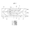
図1は、本実施の形態の半導体装置の要部断面図であり、図2〜図5は、本実施の形態の半導体装置の要部平面図である。図1には、本実施の形態の半導体装置におけるMISFET形成領域およびキャパシタ形成領域の断面図が示され、図2〜図5には、本実施の形態の半導体装置におけるキャパシタ形成領域の平面図が示されている。 FIG. 1 is a cross-sectional view of main parts of the semiconductor device of the present embodiment, and FIGS. 2 to 5 are plan views of main parts of the semiconductor device of the present embodiment. 1 is a cross-sectional view of a MISFET formation region and a capacitor formation region in the semiconductor device of the present embodiment, and FIGS. 2 to 5 are plan views of the capacitor formation region in the semiconductor device of the present embodiment. It is shown.
図1におけるキャパシタ形成領域の断面図は、図2〜図5のA1−A1線の位置での断面にほぼ対応している。但し、図1の断面図では、絶縁膜IL6および絶縁膜IL6に埋め込まれた配線M5よりも上層の構造は、図示を省略している。また、図1におけるMISFET形成領域とキャパシタ形成領域とは、同じ半導体装置(同じ半導体基板SB)における互いに異なる平面領域に対応している。図1におけるMISFET形成領域とキャパシタ形成領域とは、互いに隣り合っていても、隣り合っていなくてもよいが、理解を簡単にするために、図1の断面図においては、MISFET形成領域の断面図の隣にキャパシタ形成領域の断面図を示している。 1 substantially corresponds to the cross section taken along the line A1-A1 in FIGS. However, in the cross-sectional view of FIG. 1, the illustration of the insulating film IL6 and the structure above the wiring M5 embedded in the insulating film IL6 is omitted. Further, the MISFET formation region and the capacitor formation region in FIG. 1 correspond to different planar regions in the same semiconductor device (the same semiconductor substrate SB). The MISFET formation region and the capacitor formation region in FIG. 1 may or may not be adjacent to each other, but for the sake of easy understanding, the cross-sectional view of FIG. A sectional view of the capacitor formation region is shown next to the figure.
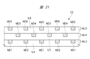
また、図2〜図5には、同じ半導体装置(半導体基板SB)における同じ平面領域(ここではキャパシタ形成領域)が示されているが、図2〜図5では、示される層が相違している。すなわち、図3には、キャパシタ形成領域における上部電極UEが形成された層(すなわち配線層ML3)の平面レイアウトが示され、図4には、キャパシタ形成領域における浮遊電極FEが形成された層(すなわち配線層ML2)の平面レイアウトが示され、図5には、キャパシタ形成領域における下部電極LEが形成された層(すなわち配線層ML1)の平面レイアウトが示されている。また、図2には、図3〜図5を重ね合わせた平面レイアウトが示されている。 2 to 5 show the same planar region (capacitor formation region here) in the same semiconductor device (semiconductor substrate SB), but the layers shown in FIGS. 2 to 5 are different. Yes. That is, FIG. 3 shows a planar layout of the layer in which the upper electrode UE is formed in the capacitor formation region (that is, the wiring layer ML3), and FIG. 4 shows the layer in which the floating electrode FE is formed in the capacitor formation region ( That is, a planar layout of the wiring layer ML2) is shown, and FIG. 5 shows a planar layout of the layer in which the lower electrode LE is formed in the capacitor formation region (that is, the wiring layer ML1). Further, FIG. 2 shows a planar layout in which FIGS.
本実施の形態の半導体装置は、MISFET形成領域にMISFET(Metal Insulator Semiconductor Field Effect Transistor)が形成され、MISFET形成領域とは異なる領域(平面領域)であるキャパシタ形成領域に容量素子C1が形成されている。本実施の形態の半導体装置の具体的な構成を図1〜図5を参照して説明する。 In the semiconductor device of this embodiment, a MISFET (Metal Insulator Semiconductor Field Effect Transistor) is formed in a MISFET formation region, and a capacitor element C1 is formed in a capacitor formation region that is a region (planar region) different from the MISFET formation region. Yes. A specific configuration of the semiconductor device of the present embodiment will be described with reference to FIGS.
図1に示されるように、本実施の形態の半導体装置を構成する半導体基板SBは、例えば1〜10Ωcm程度の比抵抗を有するp型の単結晶シリコンなどからなる。本実施の形態の半導体装置を形成する半導体基板SBは、容量素子C1が形成されたキャパシタ形成領域と、MISFETのような電界効果トランジスタが形成されたMISFET形成領域とを有しており、図1には、このキャパシタ形成領域とMISFET形成領域の断面図が示されている。 As shown in FIG. 1, the semiconductor substrate SB constituting the semiconductor device of the present embodiment is made of, for example, p-type single crystal silicon having a specific resistance of about 1 to 10 Ωcm. The semiconductor substrate SB forming the semiconductor device of the present embodiment has a capacitor forming region in which the capacitor element C1 is formed and a MISFET forming region in which a field effect transistor such as a MISFET is formed. FIG. 2 shows a cross-sectional view of the capacitor formation region and the MISFET formation region.
図1に示されるように、半導体基板SBの主面には、素子分離領域STが形成されている。素子分離領域STは、半導体基板SBに形成された溝(素子分離用の溝)に酸化シリコンなどの絶縁膜を埋め込んだものである。すなわち、素子分離領域STは、半導体基板SBに形成されかつ絶縁膜が埋め込まれた溝からなる。素子分離領域STは、STI(Shallow Trench Isolation)法により形成することができる。 As shown in FIG. 1, an element isolation region ST is formed on the main surface of the semiconductor substrate SB. The element isolation region ST is formed by embedding an insulating film such as silicon oxide in a groove (element isolation groove) formed in the semiconductor substrate SB. That is, the element isolation region ST is formed of a trench formed in the semiconductor substrate SB and embedded with an insulating film. The element isolation region ST can be formed by an STI (Shallow Trench Isolation) method.
素子分離領域STによって活性領域が規定される。活性領域は、半導体基板SBの基板領域であり、半導体基板SBの主面において素子分離領域STが形成されていない領域に対応する。 An active region is defined by the element isolation region ST. The active region is a substrate region of the semiconductor substrate SB and corresponds to a region where the element isolation region ST is not formed on the main surface of the semiconductor substrate SB.
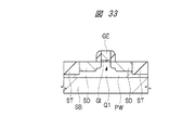
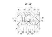
図1に示されるように、MISFET形成領域の半導体基板SBにp型ウエル領域PWが形成されており、このp型ウエル領域PW上には、nチャネル型のMISFET(Metal Insulator Semiconductor Field Effect Transistor:MIS型電界効果トランジスタ)Q1が形成されている。MISFETQ1は、p型ウエル領域PWの表面に形成されたゲート絶縁膜GIと、ゲート絶縁膜GI上に形成されたゲート電極GEと、p型ウエル領域PW内に形成されたソース・ドレイン用のn型半導体領域SDとを有している。すなわち、ゲート電極GEは、p型ウエル領域PW上にゲート絶縁膜GIを介して形成されている。また、ソース・ドレイン用のn型半導体領域SDは、半導体基板SB(p型ウエル領域PW)において、ゲート電極GEの両側の領域に形成されている。半導体基板SB(p型ウエル領域PW)における、ゲート電極GEの下の領域が、MISFETQ1のチャネルが形成される領域、すなわちチャネル形成領域となる。一対のn型半導体領域SDが、チャネル形成領域を間に挟んでゲート電極GEのゲート長方向に対向している。 As shown in FIG. 1, a p-type well region PW is formed in a semiconductor substrate SB in a MISFET formation region, and an n-channel type MISFET (Metal Insulator Semiconductor Field Effect Transistor :) is formed on the p-type well region PW. MIS type field effect transistor) Q1 is formed. The MISFET Q1 includes a gate insulating film GI formed on the surface of the p-type well region PW, a gate electrode GE formed on the gate insulating film GI, and n for source / drain formed in the p-type well region PW. Type semiconductor region SD. That is, the gate electrode GE is formed on the p-type well region PW via the gate insulating film GI. The source / drain n-type semiconductor regions SD are formed in regions on both sides of the gate electrode GE in the semiconductor substrate SB (p-type well region PW). A region under the gate electrode GE in the semiconductor substrate SB (p-type well region PW) is a region where a channel of the MISFET Q1 is formed, that is, a channel formation region. A pair of n-type semiconductor regions SD are opposed to each other in the gate length direction of the gate electrode GE with the channel formation region interposed therebetween.
ゲート絶縁膜GIは、例えば酸化シリコン膜などからなり、ゲート電極GEは、例えば、不純物を導入した多結晶シリコン膜などからなる。n型半導体領域SDは、LDD(Lightly doped Drain)構造とすることもでき、この場合、ゲート電極GEの側壁上には、サイドウォールスペーサとも称される側壁絶縁膜が形成される。 The gate insulating film GI is made of, for example, a silicon oxide film, and the gate electrode GE is made of, for example, a polycrystalline silicon film into which impurities are introduced. The n-type semiconductor region SD may have an LDD (Lightly doped Drain) structure. In this case, a sidewall insulating film, also referred to as a sidewall spacer, is formed on the sidewall of the gate electrode GE.
ゲート電極GEおよびn型半導体領域SDの表面(表層部分)には、サリサイド(Salicide:Self Aligned Silicide)技術などにより、それぞれ金属シリサイド層(図示せず)を形成することもできる。この金属シリサイド層としては、例えばコバルトシリサイド層またはニッケルシリサイド層などを用いることができる。 Metal silicide layers (not shown) can also be formed on the surfaces (surface layer portions) of the gate electrode GE and the n-type semiconductor region SD by a salicide (Salicide: Self Aligned Silicide) technique, respectively. As this metal silicide layer, for example, a cobalt silicide layer or a nickel silicide layer can be used.
また、半導体基板SBの主面にnチャネル型のMISFETQ1を形成した場合について図示および説明したが、導電型を反対にして、pチャネル型のMISFETを形成することもできる。また、半導体基板SBの主面に、nチャネル型のMISFETとpチャネル型のMISFETの両方を形成することもできる。半導体基板SBの主面に形成するMISFETの数は、種々変更可能である。また、MISFET以外の半導体素子を半導体基板SBの主面に形成することもできる。 Further, although the case where the n-channel type MISFET Q1 is formed on the main surface of the semiconductor substrate SB has been illustrated and described, a p-channel type MISFET can be formed by reversing the conductivity type. In addition, both an n-channel MISFET and a p-channel MISFET can be formed on the main surface of the semiconductor substrate SB. The number of MISFETs formed on the main surface of the semiconductor substrate SB can be variously changed. Further, a semiconductor element other than the MISFET can be formed on the main surface of the semiconductor substrate SB.
また、図1では、キャパシタ形成領域における半導体基板SBの主面には、半導体素子を形成していない場合が示されており、キャパシタ形成領域における半導体基板SBの主面には、素子分離領域STが形成されている。他の形態として、キャパシタ形成領域の半導体基板SBの主面に、例えばMISFETまたはMOS(Metal Oxide Semiconductor)型容量素子などの半導体素子を形成することもできる。 FIG. 1 shows a case where no semiconductor element is formed on the main surface of the semiconductor substrate SB in the capacitor formation region, and an element isolation region ST is formed on the main surface of the semiconductor substrate SB in the capacitor formation region. Is formed. As another form, a semiconductor element such as a MISFET or a MOS (Metal Oxide Semiconductor) type capacitive element can be formed on the main surface of the semiconductor substrate SB in the capacitor formation region.
図1に示されるように、半導体基板SBの主面(主面全面)上に、ゲート電極GEを覆うように、絶縁膜(層間絶縁膜)IL1が形成されている。絶縁膜IL1は、窒化シリコン膜(下層側)とそれよりも厚い酸化シリコン膜(上層側)との積層膜、あるいは酸化シリコン膜の単体膜などにより形成されている。 As shown in FIG. 1, an insulating film (interlayer insulating film) IL1 is formed on the main surface (entire main surface) of the semiconductor substrate SB so as to cover the gate electrode GE. The insulating film IL1 is formed of a laminated film of a silicon nitride film (lower layer side) and a thicker silicon oxide film (upper layer side), or a single film of a silicon oxide film.
絶縁膜IL1を成膜したときには、下地の段差(例えばゲート電極GEの段差など)に起因して絶縁膜IL1の上面に凹凸形状が形成されるが、絶縁膜IL1の成膜後に絶縁膜IL1の上面(表面)をCMP(Chemical Mechanical Polishing:化学的機械的研磨)法により研磨するなどして、絶縁膜IL1の上面は平坦化されている。このため、絶縁膜IL1よりも上の構造(後述の配線M1〜M5を含む多層配線構造)は、絶縁膜IL1の平坦な上面(表面)上に形成されている。 When the insulating film IL1 is formed, an uneven shape is formed on the upper surface of the insulating film IL1 due to a base step (for example, a step of the gate electrode GE). The upper surface of the insulating film IL1 is flattened by polishing the upper surface (surface) by a CMP (Chemical Mechanical Polishing) method. Therefore, the structure above the insulating film IL1 (a multilayer wiring structure including wirings M1 to M5 described later) is formed on the flat upper surface (front surface) of the insulating film IL1.
絶縁膜IL1には、絶縁膜IL1を貫通するコンタクトホール(開口部、孔、貫通孔)が形成されており、コンタクトホール内には、タングステン(W)膜を主体とする導電膜などからなるプラグ(導体部、接続用導体部)PGが形成されて埋め込まれている。MISFET形成領域において、コンタクトホールおよびそれを埋めるプラグPGは、n型半導体領域SDの上部やゲート電極GEの上部などに形成されている。 The insulating film IL1 has contact holes (openings, holes, through holes) penetrating the insulating film IL1, and plugs made of a conductive film mainly composed of a tungsten (W) film are formed in the contact holes. (Conductor part, connecting conductor part) PG is formed and embedded. In the MISFET formation region, the contact hole and the plug PG filling the contact hole are formed above the n-type semiconductor region SD, the top of the gate electrode GE, and the like.
図1に示されるように、絶縁膜IL1上には、配線M1〜M5を含む複数の配線層、すなわち多層配線構造が形成されている。 As shown in FIG. 1, a plurality of wiring layers including wirings M1 to M5, that is, a multilayer wiring structure is formed on the insulating film IL1.
すなわち、プラグPGが埋め込まれた絶縁膜IL1上には、絶縁膜(層間絶縁膜)IL2が形成されており、この絶縁膜IL2には配線用の溝とこの溝に埋め込まれた配線M1とが形成されている。絶縁膜IL2は、単層の絶縁膜、あるいは、複数の絶縁膜の積層膜とすることができる。配線M1は、ダマシン(Damascene)技術(ここではシングルダマシン技術)を用いて形成することができ、銅を主成分とする銅配線(ダマシン銅配線、埋込銅配線)とすることができる。 That is, an insulating film (interlayer insulating film) IL2 is formed on the insulating film IL1 in which the plug PG is embedded, and a wiring groove and a wiring M1 embedded in the groove are formed in the insulating film IL2. Is formed. The insulating film IL2 can be a single-layer insulating film or a stacked film of a plurality of insulating films. The wiring M1 can be formed using a damascene technology (here, a single damascene technology), and can be a copper wiring (damascene copper wiring, embedded copper wiring) containing copper as a main component.
配線M1は、多層配線構造における最下層の配線層(すなわち配線層ML1)の配線である。ここで、半導体基板SB上(すなわち絶縁膜IL1上)に形成された多層配線構造において、最下層の配線層を、符号ML1を付して配線層ML1と称することとする。また、半導体基板SB上(すなわち絶縁膜IL1上)に形成された多層配線構造において、配線層ML1よりも1つ上層の配線層を、符号ML2を付して配線層ML2と称し、配線層ML2よりも1つ上層の配線層を、符号ML3を付して配線層ML3と称することとする。また、半導体基板SB上(すなわち絶縁膜IL1上)に形成された多層配線構造において、配線層ML3よりも1つ上層の配線層を、符号ML4を付して配線層ML4と称し、配線層ML4よりも1つ上層の配線層を、符号ML5を付して配線層ML5と称することとする。従って、配線M1は、配線層ML1の配線であり、後述の配線M2は、配線層ML2の配線であり、後述の配線M3は、配線層ML3の配線であり、後述の配線M4は、配線層ML4の配線であり、後述の配線M5は、配線層ML5の配線である。 The wiring M1 is a wiring of the lowermost wiring layer (that is, the wiring layer ML1) in the multilayer wiring structure. Here, in the multilayer wiring structure formed on the semiconductor substrate SB (that is, on the insulating film IL1), the lowermost wiring layer is denoted by a reference numeral ML1 and is referred to as a wiring layer ML1. In the multilayer wiring structure formed on the semiconductor substrate SB (that is, on the insulating film IL1), the wiring layer that is one layer above the wiring layer ML1 is referred to as a wiring layer ML2 with a reference numeral ML2, and the wiring layer ML2 The wiring layer that is one layer higher than that is denoted by a reference numeral ML3 and is referred to as a wiring layer ML3. In the multilayer wiring structure formed on the semiconductor substrate SB (that is, on the insulating film IL1), the wiring layer that is one layer above the wiring layer ML3 is referred to as a wiring layer ML4 with a reference numeral ML4, and the wiring layer ML4. The wiring layer that is one layer higher than that is denoted by the reference numeral ML5 and is referred to as a wiring layer ML5. Accordingly, the wiring M1 is a wiring of the wiring layer ML1, a wiring M2 described later is a wiring of the wiring layer ML2, a wiring M3 described later is a wiring of the wiring layer ML3, and a wiring M4 described later is a wiring layer. ML4 is a wiring, and a wiring M5 described later is a wiring of the wiring layer ML5.
なお、図1には符号ML1〜ML5は示していないが、図1において、配線M1および下部電極LEが形成されている層が配線層ML1に対応し、配線M2および浮遊電極FEが形成されている層が配線層ML2に対応し、配線M3および上部電極UEが形成されている層が配線層ML3に対応している。また、図1において、配線M4が形成されている層が配線層ML4に対応し、配線M5が形成されている層が配線層ML5に対応している。 In FIG. 1, reference numerals ML1 to ML5 are not shown. In FIG. 1, the layer in which the wiring M1 and the lower electrode LE are formed corresponds to the wiring layer ML1, and the wiring M2 and the floating electrode FE are formed. The layer in which the wiring M3 and the upper electrode UE are formed corresponds to the wiring layer ML3. In FIG. 1, the layer in which the wiring M4 is formed corresponds to the wiring layer ML4, and the layer in which the wiring M5 is formed corresponds to the wiring layer ML5.
図1〜図5に示されるように、キャパシタ形成領域においては、下部電極LEが、配線M1と同層に同工程で形成されている。すなわち、配線M1と下部電極LEとは、同じ配線層ML1に形成されている。このため、配線M1と下部電極LEとは、どちらもダマシン技術を用いて同工程で形成されており、絶縁膜IL2に埋め込まれている。具体的には、配線M1と下部電極LEとは、それぞれ、絶縁膜IL2に形成された溝(または開口部)に埋め込まれている。下部電極LEと配線M1とは、同じ導電材料からなる。また、下部電極LEには、配線M1が一体的に接続されており、この下部電極LEに接続された配線M1などを介して、下部電極LEに所定の電位が供給できるようになっている。 As shown in FIGS. 1 to 5, in the capacitor formation region, the lower electrode LE is formed in the same layer as the wiring M1 in the same process. That is, the wiring M1 and the lower electrode LE are formed in the same wiring layer ML1. For this reason, both the wiring M1 and the lower electrode LE are formed in the same process using the damascene technique, and are embedded in the insulating film IL2. Specifically, the wiring M1 and the lower electrode LE are embedded in grooves (or openings) formed in the insulating film IL2. The lower electrode LE and the wiring M1 are made of the same conductive material. In addition, a wiring M1 is integrally connected to the lower electrode LE, and a predetermined potential can be supplied to the lower electrode LE through the wiring M1 connected to the lower electrode LE.
図1に示されるように、配線M1および下部電極LEが埋め込まれた絶縁膜IL2上には、絶縁膜(層間絶縁膜)IL3が形成されている。絶縁膜IL3は、単層の絶縁膜、あるいは、複数の絶縁膜の積層膜とすることができる。 As shown in FIG. 1, an insulating film (interlayer insulating film) IL3 is formed on the insulating film IL2 in which the wiring M1 and the lower electrode LE are embedded. The insulating film IL3 can be a single-layer insulating film or a stacked film of a plurality of insulating films.
絶縁膜IL3には、配線用の溝とその溝に埋め込まれた配線M2とが形成されている。配線M2は、ダマシン技術(ここではデュアルダマシン技術)を用いて形成することができ、銅を主成分とする銅配線(ダマシン銅配線、埋込銅配線)とすることができる。配線M2は、配線層ML2の配線である。配線M2の底面は、絶縁膜IL3の厚みの途中に位置している。 In the insulating film IL3, a trench for wiring and a wiring M2 embedded in the trench are formed. The wiring M2 can be formed using a damascene technology (here, dual damascene technology), and can be a copper wiring containing copper as a main component (damascene copper wiring, embedded copper wiring). The wiring M2 is a wiring of the wiring layer ML2. The bottom surface of the wiring M2 is located in the middle of the thickness of the insulating film IL3.
配線M2は、配線M2と一体的に形成されたビア部V2を介して、配線M1と電気的に接続されている。すなわち、ビア部V2は、配線M2と配線M1との間に配置されており、ビア部V2の上面は、配線M2の下面と一体的に接続されており、ビア部V2の下面(底面)は配線M1の上面に接している。ビア部V2は配線M2と同じ導電膜により一体的に形成されており、デュアルダマシン(Dual-Damascene)技術により配線M2を形成する際に配線M2と一緒にビア部V2も形成される。ビア部V2や後述のビア部V3,V4,V5は、異なる層の配線間に配置されかつ異なる層の配線間を接続する導電性の接続部材である。 The wiring M2 is electrically connected to the wiring M1 through a via portion V2 formed integrally with the wiring M2. That is, the via portion V2 is disposed between the wiring M2 and the wiring M1, the upper surface of the via portion V2 is integrally connected to the lower surface of the wiring M2, and the lower surface (bottom surface) of the via portion V2 is It is in contact with the upper surface of the wiring M1. The via portion V2 is integrally formed of the same conductive film as the wiring M2, and the via portion V2 is formed together with the wiring M2 when the wiring M2 is formed by the dual damascene technique. A via portion V2 and via portions V3, V4, and V5, which will be described later, are conductive connection members that are arranged between wirings of different layers and connect wirings of different layers.
また、ビア部V2は、配線M2とは別工程で形成することもでき、その場合、ビア部V2はプラグPGと同様の工程により形成され、配線M2はシングルダマシン技術により形成され、ビア部V2の下面(底面)は配線M1の上面に接し、ビア部V2の上面は配線M2の下面に接することになる。 The via portion V2 can also be formed in a separate process from the wiring M2. In this case, the via portion V2 is formed by the same process as the plug PG, the wiring M2 is formed by a single damascene technique, and the via portion V2 is formed. The bottom surface (bottom surface) of the contact portion is in contact with the top surface of the wiring M1, and the top surface of the via portion V2 is in contact with the bottom surface of the wiring M2.
図1〜図5に示されるように、キャパシタ形成領域においては、浮遊電極FEが、配線M2と同層に同工程で形成されている。すなわち、配線M2と浮遊電極FEとは、同じ配線層ML2に形成されている。つまり、配線M2および浮遊電極FEは、配線M1および下部電極LEが形成された配線層ML1よりも1つ上層の配線層ML2に形成されている。このため、配線M2と浮遊電極FEとは、どちらもダマシン技術を用いて同工程で形成されており、絶縁膜IL3に埋め込まれている。具体的には、配線M2と浮遊電極FEとは、それぞれ、絶縁膜IL3に形成された溝(または開口部)に埋め込まれている。浮遊電極FEと配線M2とは、同じ導電材料からなる。浮遊電極FEの底面(下面)は、絶縁膜IL3の厚みの途中に位置している。浮遊電極FEの底面(下面)の高さ位置と、配線M2の底面(下面)の高さ位置とは、概ね同じである。なお、絶縁膜に溝を形成する際には、その平面寸法が大きいほど溝の深さは深くなるため、浮遊電極FEの寸法(辺の寸法)が配線M2の幅よりも大きいことを反映して、浮遊電極FEの底面の高さ位置が、配線M2の底面の高さ位置より低くなる場合もある。 As shown in FIGS. 1 to 5, in the capacitor formation region, the floating electrode FE is formed in the same layer as the wiring M2 in the same process. That is, the wiring M2 and the floating electrode FE are formed in the same wiring layer ML2. That is, the wiring M2 and the floating electrode FE are formed in the wiring layer ML2 that is one layer higher than the wiring layer ML1 in which the wiring M1 and the lower electrode LE are formed. For this reason, both the wiring M2 and the floating electrode FE are formed in the same process using the damascene technique, and are embedded in the insulating film IL3. Specifically, the wiring M2 and the floating electrode FE are each embedded in a groove (or opening) formed in the insulating film IL3. The floating electrode FE and the wiring M2 are made of the same conductive material. The bottom surface (lower surface) of the floating electrode FE is located in the middle of the thickness of the insulating film IL3. The height position of the bottom surface (lower surface) of the floating electrode FE and the height position of the bottom surface (lower surface) of the wiring M2 are substantially the same. Note that when the trench is formed in the insulating film, the depth of the trench becomes deeper as the planar dimension is larger, which reflects that the dimension (side dimension) of the floating electrode FE is larger than the width of the wiring M2. Thus, the height position of the bottom surface of the floating electrode FE may be lower than the height position of the bottom surface of the wiring M2.
浮遊電極FEは、浮遊電位とされている。すなわち、浮遊電極FEは、電気的に浮遊状態(フローティング状態)とされている。浮遊電極FEは、下部電極LEと導体では繋がっておらず、また、後述の上部電極UEと導体では繋がっていない。このため、浮遊電極FEにはビア部V2は接続されておらず、浮遊電極FEの下にはビア部V2は配置されていない。 The floating electrode FE is set to a floating potential. That is, the floating electrode FE is in an electrically floating state (floating state). The floating electrode FE is not connected to the lower electrode LE by a conductor, and is not connected to an upper electrode UE, which will be described later, by a conductor. For this reason, the via part V2 is not connected to the floating electrode FE, and the via part V2 is not disposed under the floating electrode FE.
下部電極LEおよび上部電極UEのうちの一方に、下部電極LEおよび上部電極UEのうちの他方よりも高い電位(電圧)が印加(供給)されることにより、容量素子C1に電荷が蓄積される。すなわち、容量素子C1に電荷を蓄積する際には、配線などの導体を通じて下部電極LEと上部電極UEとに互いに異なる電圧が印加される。つまり、容量素子C1に電荷を蓄積する際には、下部電極LEよりも上部電極UEが高電位(高電圧)とされるか、あるいは、上部電極UEよりも下部電極LEが高電位(高電圧)とされる。しかしながら、浮遊電極FEは、浮遊電位とされており、容量素子C1に電荷を蓄積する際に、配線などの導体を通じた電圧印加は浮遊電極FEに対しては行われない。このため、浮遊電極FEは、ダミー電極とみなすこともできる。 When a potential (voltage) higher than the other of the lower electrode LE and the upper electrode UE is applied (supplied) to one of the lower electrode LE and the upper electrode UE, charges are accumulated in the capacitive element C1. . That is, when accumulating charges in the capacitive element C1, different voltages are applied to the lower electrode LE and the upper electrode UE through a conductor such as a wiring. That is, when accumulating charges in the capacitive element C1, the upper electrode UE is set to a higher potential (high voltage) than the lower electrode LE, or the lower electrode LE is set to a higher potential (high voltage) than the upper electrode UE. ). However, the floating electrode FE is at a floating potential, and voltage is not applied to the floating electrode FE through a conductor such as a wiring when charges are accumulated in the capacitor C1. For this reason, the floating electrode FE can also be regarded as a dummy electrode.
図1に示されるように、配線M2および浮遊電極FEが埋め込まれた絶縁膜IL3上には、絶縁膜(層間絶縁膜)IL4が形成されている。絶縁膜IL4は、単層の絶縁膜、あるいは、複数の絶縁膜の積層膜とすることができる。 As shown in FIG. 1, an insulating film (interlayer insulating film) IL4 is formed on the insulating film IL3 in which the wiring M2 and the floating electrode FE are embedded. The insulating film IL4 can be a single-layer insulating film or a stacked film of a plurality of insulating films.
絶縁膜IL4には、配線用の溝とその溝に埋め込まれた配線M3とが形成されている。配線M3は、ダマシン技術(ここではデュアルダマシン技術)を用いて形成することができ、銅を主成分とする銅配線(ダマシン銅配線、埋込銅配線)とすることができる。配線M3は、配線層ML3の配線である。配線M3の底面は、絶縁膜IL4の厚みの途中に位置している。 In the insulating film IL4, a trench for wiring and a wiring M3 embedded in the trench are formed. The wiring M3 can be formed using a damascene technique (here, dual damascene technique), and can be a copper wiring (a damascene copper wiring or a buried copper wiring) containing copper as a main component. The wiring M3 is a wiring of the wiring layer ML3. The bottom surface of the wiring M3 is located in the middle of the thickness of the insulating film IL4.
配線M3は、配線M3と一体的に形成されたビア部V3を介して、配線M2と電気的に接続されている。すなわち、ビア部V3は、配線M3と配線M2との間に配置されており、ビア部V3の上面は、配線M3の下面と一体的に接続されており、ビア部V3の下面(底面)は配線M2の上面に接している。ビア部V3は配線M3と同じ導電膜により一体的に形成されており、デュアルダマシン技術により配線M3を形成する際に配線M3と一緒にビア部V3も形成される。 The wiring M3 is electrically connected to the wiring M2 through a via portion V3 formed integrally with the wiring M3. That is, the via portion V3 is disposed between the wiring M3 and the wiring M2, the upper surface of the via portion V3 is integrally connected to the lower surface of the wiring M3, and the lower surface (bottom surface) of the via portion V3 is It is in contact with the upper surface of the wiring M2. The via portion V3 is integrally formed of the same conductive film as the wiring M3. When the wiring M3 is formed by the dual damascene technique, the via portion V3 is also formed together with the wiring M3.
また、ビア部V3は、配線M3とは別工程で形成することもでき、その場合、ビア部V3はプラグPGと同様の工程により形成され、配線M3はシングルダマシン技術により形成され、ビア部V3の下面(底面)は配線M2の上面に接し、ビア部V3の上面は配線M3の下面に接することになる。 The via portion V3 can also be formed in a separate process from the wiring M3. In that case, the via portion V3 is formed by the same process as the plug PG, the wiring M3 is formed by a single damascene technique, and the via portion V3. The bottom surface (bottom surface) of the contact portion is in contact with the top surface of the wiring M2, and the top surface of the via portion V3 is in contact with the bottom surface of the wiring M3.
図1〜図5に示されるように、キャパシタ形成領域においては、上部電極UEが、配線M3と同層に同工程で形成されている。すなわち、配線M3と上部電極UEとは、同じ配線層ML3に形成されている。つまり、配線M3および上部電極UEは、配線M2および浮遊電極FEが形成された配線層ML2よりも1つ上層の配線層ML3に形成されている。このため、配線M3と上部電極UEとは、どちらもダマシン技術を用いて同工程で形成されており、絶縁膜IL4に埋め込まれている。具体的には、配線M3と上部電極UEとは、それぞれ、絶縁膜IL4に形成された溝(または開口部)に埋め込まれている。上部電極UEと配線M3とは、同じ導電材料からなる。上部電極UEの底面(下面)は、絶縁膜IL4の厚みの途中に位置している。上部電極UEの底面(下面)の高さ位置と、配線M3の底面(下面)の高さ位置とは、概ね同じである。なお、絶縁膜に溝を形成する際には、その平面寸法が大きいほど溝の深さは深くなるため、上部電極UEの寸法(辺の寸法)が配線M3の幅よりも大きいことを反映して、上部電極UEの底面の高さ位置が、配線M3の底面の高さ位置より低くなる場合もある。また、上部電極UEには、配線M3が一体的に接続されており、この上部電極UEに接続された配線M3などを介して、上部電極UEに所定の電位が供給できるようになっている。 As shown in FIGS. 1 to 5, in the capacitor formation region, the upper electrode UE is formed in the same layer as the wiring M3 in the same process. That is, the wiring M3 and the upper electrode UE are formed in the same wiring layer ML3. That is, the wiring M3 and the upper electrode UE are formed in the wiring layer ML3 that is one layer higher than the wiring layer ML2 in which the wiring M2 and the floating electrode FE are formed. For this reason, the wiring M3 and the upper electrode UE are both formed in the same process using the damascene technique, and are embedded in the insulating film IL4. Specifically, the wiring M3 and the upper electrode UE are each embedded in a groove (or an opening) formed in the insulating film IL4. The upper electrode UE and the wiring M3 are made of the same conductive material. The bottom surface (lower surface) of the upper electrode UE is located in the middle of the thickness of the insulating film IL4. The height position of the bottom surface (lower surface) of the upper electrode UE and the height position of the bottom surface (lower surface) of the wiring M3 are substantially the same. Note that, when the trench is formed in the insulating film, the depth of the trench becomes deeper as the planar dimension is larger, which reflects that the dimension (side dimension) of the upper electrode UE is larger than the width of the wiring M3. Thus, the height position of the bottom surface of the upper electrode UE may be lower than the height position of the bottom surface of the wiring M3. Further, a wiring M3 is integrally connected to the upper electrode UE, and a predetermined potential can be supplied to the upper electrode UE through the wiring M3 connected to the upper electrode UE.
キャパシタ形成領域において、下部電極LEの上方に浮遊電極FEが配置され、浮遊電極FEの上方に上部電極UEが配置されている。上部電極UEと浮遊電極FEとは、導体では接続されていない。すなわち、上部電極UEと浮遊電極FEとの間には、直流電流は流れないようになっている。また、下部電極LEと浮遊電極FEとは、導体では接続されていない。すなわち、下部電極LEと浮遊電極FEとの間には、直流電流は流れないようになっている。また、上部電極UEと下部電極LEとは、導体では接続されていない。すなわち、上部電極UEと下部電極LEとの間には、直流電流は流れないようになっている。このため、上部電極UEと浮遊電極FEとの間には、上部電極UEと浮遊電極FEとを電気的に接続するビア部V3は配置されておらず、また、下部電極LEと浮遊電極FEとの間には、下部電極LEと浮遊電極FEとを電気的に接続するビア部V2は配置されていない。 In the capacitor formation region, the floating electrode FE is disposed above the lower electrode LE, and the upper electrode UE is disposed above the floating electrode FE. The upper electrode UE and the floating electrode FE are not connected by a conductor. That is, no direct current flows between the upper electrode UE and the floating electrode FE. Further, the lower electrode LE and the floating electrode FE are not connected by a conductor. That is, no direct current flows between the lower electrode LE and the floating electrode FE. Further, the upper electrode UE and the lower electrode LE are not connected by a conductor. That is, no direct current flows between the upper electrode UE and the lower electrode LE. For this reason, the via portion V3 that electrically connects the upper electrode UE and the floating electrode FE is not disposed between the upper electrode UE and the floating electrode FE, and the lower electrode LE and the floating electrode FE Between these, the via portion V2 that electrically connects the lower electrode LE and the floating electrode FE is not disposed.
なお、本願において、導体からなる複数の部材(電極または配線などに対応)の接続関係をいうときに、「導体では接続されていない」または「導体では繋がっていない」と表現するときは、導体でつながる導電経路が部材間に形成されていないことを意味している。 In this application, when referring to the connection relationship of a plurality of members made of conductors (corresponding to electrodes or wirings), when expressing as “not connected by a conductor” or “not connected by a conductor” This means that the conductive path connected by is not formed between the members.
下部電極LEと、上部電極UEと、下部電極LEと上部電極UEとの間の絶縁膜IL3,IL4とにより、容量素子(キャパシタ)C1が形成されている。下部電極LEは、容量素子C1の一方の電極であり、上部電極UEは、容量素子C1の他方の電極であり、下部電極LEと上部電極UEとの間に介在する絶縁膜IL3,IL4が、容量素子C1の容量絶縁膜(誘電体膜)として機能する。容量素子C1は、MIM(Metal Insulator Metal)型の容量素子である。 A capacitive element (capacitor) C1 is formed by the lower electrode LE, the upper electrode UE, and the insulating films IL3 and IL4 between the lower electrode LE and the upper electrode UE. The lower electrode LE is one electrode of the capacitive element C1, the upper electrode UE is the other electrode of the capacitive element C1, and the insulating films IL3 and IL4 interposed between the lower electrode LE and the upper electrode UE include It functions as a capacitive insulating film (dielectric film) of the capacitive element C1. The capacitive element C1 is a MIM (Metal Insulator Metal) type capacitive element.
但し、容量素子C1においては、下部電極LEと上部電極UEとの間に、浮遊電極FEが配置されている。このため、下部電極LEと浮遊電極FEとの間に介在する絶縁膜IL3と、上部電極UEと浮遊電極FEとの間に介在する絶縁膜IL4とが、容量素子C1の容量絶縁膜(誘電体膜)として機能することになる。キャパシタ形成領域に、下部電極LEと浮遊電極FEと上部電極UEとが下から順に形成されることで、容量素子C1を形成することができる。 However, in the capacitive element C1, the floating electrode FE is disposed between the lower electrode LE and the upper electrode UE. For this reason, the insulating film IL3 interposed between the lower electrode LE and the floating electrode FE and the insulating film IL4 interposed between the upper electrode UE and the floating electrode FE form a capacitive insulating film (dielectric material) of the capacitive element C1. Film). The capacitor element C1 can be formed by forming the lower electrode LE, the floating electrode FE, and the upper electrode UE in this order from the bottom in the capacitor formation region.
下部電極LEは、図5に示されるように、例えば矩形状の平面形状とすることができ、また、浮遊電極FEは、図4に示されるように、例えば矩形状の平面形状とすることができ、上部電極UEは、図3に示されるように、例えば矩形状の平面形状とすることができる。また、下部電極LEと上部電極UEとで、平面形状および平面寸法(平面積)を同じにして、平面視で下部電極LEと上部電極UEとが重なる(一致する)ようにすることもでき、そうすることで、容量素子C1の占有面積を抑えながら容量素子C1の容量値を増やすことができる。 As shown in FIG. 5, the lower electrode LE can have a rectangular planar shape, for example, and the floating electrode FE can have a rectangular planar shape as shown in FIG. In addition, the upper electrode UE can have, for example, a rectangular planar shape as shown in FIG. In addition, the lower electrode LE and the upper electrode UE can have the same planar shape and planar dimensions (planar area) so that the lower electrode LE and the upper electrode UE overlap (match) in plan view. By doing so, the capacitance value of the capacitive element C1 can be increased while suppressing the area occupied by the capacitive element C1.
なお、「平面視」または「平面的に見て」と言うときは、半導体基板SBの主面に平行な平面で見た場合を言うものとする。 Note that “plan view” or “view in plan” refers to the case of viewing in a plane parallel to the main surface of the semiconductor substrate SB.
図1に示されるように、配線M3および上部電極UEが埋め込まれた絶縁膜IL4上には、絶縁膜(層間絶縁膜)IL5が形成されている。絶縁膜IL5は、単層の絶縁膜、あるいは、複数の絶縁膜の積層膜とすることができる。 As shown in FIG. 1, an insulating film (interlayer insulating film) IL5 is formed on the insulating film IL4 in which the wiring M3 and the upper electrode UE are embedded. The insulating film IL5 can be a single-layer insulating film or a stacked film of a plurality of insulating films.
絶縁膜IL5には、配線用の溝とその溝に埋め込まれた配線M4とが形成されている。配線M4は、ダマシン技術(ここではデュアルダマシン技術)を用いて形成することができ、銅を主成分とする銅配線(ダマシン銅配線、埋込銅配線)とすることができる。配線M4は、配線層ML4の配線である。配線M4の底面(下面)は、絶縁膜IL5の厚みの途中に位置している。 In the insulating film IL5, a trench for wiring and a wiring M4 embedded in the trench are formed. The wiring M4 can be formed using a damascene technique (here, dual damascene technique), and can be a copper wiring (a damascene copper wiring or a buried copper wiring) containing copper as a main component. The wiring M4 is a wiring of the wiring layer ML4. The bottom surface (lower surface) of the wiring M4 is located in the middle of the thickness of the insulating film IL5.
配線M4は、配線M4と一体的に形成されたビア部V4を介して、配線M3と電気的に接続されている。すなわち、ビア部V4は、配線M4と配線M3との間に配置されており、ビア部V4の上面は、配線M4の下面と一体的に接続されており、ビア部V4の下面(底面)は配線M3の上面に接している。ビア部V4は配線M4と同じ導電膜により一体的に形成されており、デュアルダマシン技術により配線M4を形成する際に配線M4と一緒にビア部V4も形成される。 The wiring M4 is electrically connected to the wiring M3 through a via portion V4 formed integrally with the wiring M4. That is, the via portion V4 is disposed between the wiring M4 and the wiring M3, the upper surface of the via portion V4 is integrally connected to the lower surface of the wiring M4, and the lower surface (bottom surface) of the via portion V4 is It is in contact with the upper surface of the wiring M3. The via portion V4 is integrally formed of the same conductive film as the wiring M4. When the wiring M4 is formed by the dual damascene technique, the via portion V4 is also formed together with the wiring M4.
また、ビア部V4は、配線M4とは別工程で形成することもでき、その場合、ビア部V4はプラグPGと同様の工程により形成され、配線M4はシングルダマシン技術により形成され、ビア部V4の下面(底面)は配線M3の上面に接し、ビア部V4の上面は配線M4の下面に接することになる。 The via portion V4 can also be formed in a separate process from the wiring M4. In that case, the via portion V4 is formed by the same process as the plug PG, the wiring M4 is formed by a single damascene technique, and the via portion V4. The lower surface (bottom surface) of the contact portion contacts the upper surface of the wiring M3, and the upper surface of the via portion V4 contacts the lower surface of the wiring M4.
配線M4が埋め込まれた絶縁膜IL5上には、絶縁膜(層間絶縁膜)IL6が形成されている。絶縁膜IL6は、単層の絶縁膜、あるいは、複数の絶縁膜の積層膜とすることができる。 An insulating film (interlayer insulating film) IL6 is formed over the insulating film IL5 in which the wiring M4 is embedded. The insulating film IL6 can be a single-layer insulating film or a stacked film of a plurality of insulating films.
絶縁膜IL6には、配線用の溝とその溝に埋め込まれた配線M5とが形成されている。配線M5は、ダマシン技術(ここではデュアルダマシン技術)を用いて形成することができ、銅を主成分とする銅配線(ダマシン銅配線、埋込銅配線)とすることができる。配線M5は、配線層ML5の配線である。配線M5の底面(下面)は、絶縁膜IL6の厚みの途中に位置している。 In the insulating film IL6, a trench for wiring and a wiring M5 embedded in the trench are formed. The wiring M5 can be formed using damascene technology (here, dual damascene technology) and can be copper wiring (damascene copper wiring, embedded copper wiring) containing copper as a main component. The wiring M5 is a wiring of the wiring layer ML5. The bottom surface (lower surface) of the wiring M5 is located in the middle of the thickness of the insulating film IL6.
配線M5は、配線M5と一体的に形成されたビア部V5を介して、配線M4と電気的に接続されている。すなわち、ビア部V5は、配線M5と配線M4との間に配置されており、ビア部V5の上面は、配線M5の下面と一体的に接続されており、ビア部V5の下面(底面)は配線M4の上面に接している。ビア部V5は配線M5と同じ導電膜により一体的に形成されており、デュアルダマシン技術により配線M5を形成する際に配線M5と一緒にビア部V5も形成される。 The wiring M5 is electrically connected to the wiring M4 through a via portion V5 formed integrally with the wiring M5. That is, the via portion V5 is disposed between the wiring M5 and the wiring M4, the upper surface of the via portion V5 is integrally connected to the lower surface of the wiring M5, and the lower surface (bottom surface) of the via portion V5 is It is in contact with the upper surface of the wiring M4. The via portion V5 is integrally formed of the same conductive film as the wiring M5. When the wiring M5 is formed by the dual damascene technique, the via portion V5 is also formed together with the wiring M5.
また、ビア部V5は、配線M5とは別工程で形成することもでき、その場合、ビア部V5はプラグPGと同様の工程により形成され、配線M5はシングルダマシン技術により形成され、ビア部V5の下面(底面)は配線M4の上面に接し、ビア部V5の上面は配線M5の下面に接することになる。 The via portion V5 can also be formed in a separate process from the wiring M5. In that case, the via portion V5 is formed by the same process as the plug PG, the wiring M5 is formed by a single damascene technique, and the via portion V5. The bottom surface (bottom surface) of the contact portion contacts the top surface of the wiring M4, and the top surface of the via portion V5 contacts the bottom surface of the wiring M5.
配線M5が埋め込まれた絶縁膜IL6上に、必要に応じて更に上層の絶縁膜、配線、ボンディングパッドおよび最上層の保護膜などが形成されるが、ここではその図示および説明は省略する。 On the insulating film IL6 in which the wiring M5 is embedded, an upper insulating film, wiring, bonding pad, uppermost protective film, and the like are further formed as necessary, but illustration and description thereof are omitted here.
本実施の形態では、下部電極LEが配線M1と同層に形成され、浮遊電極FEが配線M2と同層に形成され、上部電極UEが配線M3と同層に形成されている。他の形態として、下部電極LEを配線M2と同層に形成し、浮遊電極FEを配線M3と同層に形成し、上部電極UEを配線M4と同層に形成することもでき、また、更に他の形態として、下部電極LEを配線M3と同層に形成し、浮遊電極FEを配線M4と同層に形成し、上部電極UEを配線M5と同層に形成することもできる。つまり、下部電極LEを形成する配線層は変更可能であるが、下部電極LEがいずれの配線層に形成された場合も、浮遊電極FEは、下部電極LEが形成された配線層よりも1つ上層の配線層に形成し、上部電極UEは、浮遊電極FEが形成された配線層よりも1つ上層の配線層に形成する。また、配線M1〜M5だけでなく配線M5よりも上層の配線も形成している場合(すなわち配線層が6層以上の場合)は、下部電極LEを配線M3よりも上層の配線層に形成することも可能であり、その場合においても、浮遊電極FEは、下部電極LEが形成された配線層よりも1つ上層の配線層に形成し、上部電極UEは、浮遊電極FEが形成された配線層よりも1つ上層の配線層に形成する。 In the present embodiment, the lower electrode LE is formed in the same layer as the wiring M1, the floating electrode FE is formed in the same layer as the wiring M2, and the upper electrode UE is formed in the same layer as the wiring M3. As another form, the lower electrode LE may be formed in the same layer as the wiring M2, the floating electrode FE may be formed in the same layer as the wiring M3, and the upper electrode UE may be formed in the same layer as the wiring M4. As another form, the lower electrode LE may be formed in the same layer as the wiring M3, the floating electrode FE may be formed in the same layer as the wiring M4, and the upper electrode UE may be formed in the same layer as the wiring M5. That is, the wiring layer for forming the lower electrode LE can be changed, but when the lower electrode LE is formed in any wiring layer, the floating electrode FE is one more than the wiring layer in which the lower electrode LE is formed. The upper electrode UE is formed in a wiring layer one layer higher than the wiring layer in which the floating electrode FE is formed. Further, when not only the wirings M1 to M5 but also wirings higher than the wiring M5 are formed (that is, when the wiring layer has six or more layers), the lower electrode LE is formed in a wiring layer above the wiring M3. In this case as well, the floating electrode FE is formed in a wiring layer one layer higher than the wiring layer in which the lower electrode LE is formed, and the upper electrode UE is a wiring in which the floating electrode FE is formed. The wiring layer is formed one layer above the layer.
つまり、半導体基板SBの上方には、複数の配線層を含む配線構造(多層配線構造)が形成されるが、本実施の形態では、その複数の配線層のうちの連続する任意の3層の配線層に、下部電極LEと浮遊電極FEと上部電極UEとを形成すればよい。このとき、浮遊電極FEは、下部電極LEが形成された配線層よりも1つ上層の配線層に形成し、上部電極UEは、浮遊電極FEが形成された配線層よりも1つ上層の配線層に形成する必要がある。本実施の形態では、3層の配線層に下部電極LEと浮遊電極FEと上部電極UEとを形成するため、半導体基板SBの上方に形成する配線構造(多層配線構造)は、少なくとも3層の配線層を含んでいる必要がある。 That is, a wiring structure (multilayer wiring structure) including a plurality of wiring layers is formed above the semiconductor substrate SB. In this embodiment, any three consecutive layers of the plurality of wiring layers are formed. The lower electrode LE, the floating electrode FE, and the upper electrode UE may be formed in the wiring layer. At this time, the floating electrode FE is formed in a wiring layer one layer higher than the wiring layer in which the lower electrode LE is formed, and the upper electrode UE is a wiring layer one layer higher than the wiring layer in which the floating electrode FE is formed. It is necessary to form a layer. In the present embodiment, since the lower electrode LE, the floating electrode FE, and the upper electrode UE are formed in the three wiring layers, the wiring structure (multilayer wiring structure) formed above the semiconductor substrate SB has at least three layers. It is necessary to include a wiring layer.
<検討例について>
次に、本発明者が検討した検討例について説明する。
<About study example>
Next, a study example studied by the present inventors will be described.
図6は、本発明者が検討した第1検討例の半導体装置の要部断面図であり、図7は、本発明者が検討した第2検討例の半導体装置の要部断面図であり、図8は、本実施の形態の半導体装置の要部断面図である。図6〜図8には、キャパシタ形成領域における、絶縁膜IL2,IL3,IL4およびそれに埋め込まれた電極(容量素子用の電極)が示されており、絶縁膜IL1およびそれよりも下層の構造と、絶縁膜IL5およびそれよりも上層の構造については、図示を省略している。すなわち、上記図1において、キャパシタ形成領域における絶縁膜IL2,IL3,IL4およびそこに埋め込まれた電極(下部電極LEと浮遊電極FEと上部電極UE)を抜き出して示したものが、図8に対応しており、図6および図7は、第1検討例および第2検討例の場合の、この図8に相当する領域が示されたものである。 FIG. 6 is a cross-sectional view of the main part of the semiconductor device of the first study example studied by the present inventors, and FIG. 7 is a cross-sectional view of the main part of the semiconductor device of the second study example studied by the present inventor. FIG. 8 is a fragmentary cross-sectional view of the semiconductor device of the present embodiment. 6 to 8 show the insulating films IL2, IL3, and IL4 and electrodes (capacitance element electrodes) embedded in the capacitor formation region. The insulating film IL1 and the structure below it are shown in FIGS. The illustration of the insulating film IL5 and the structure above it is omitted. That is, in FIG. 1, the insulating films IL2, IL3, and IL4 in the capacitor formation region and the electrodes embedded therein (lower electrode LE, floating electrode FE, and upper electrode UE) are extracted and shown in FIG. FIG. 6 and FIG. 7 show regions corresponding to FIG. 8 in the case of the first study example and the second study example.
図6に示される第1検討例では、キャパシタ形成領域において、電極DE1が、上記配線M1と同層に同工程で形成され、また、電極DE2が、上記配線M2と同層に同工程で形成され、また、電極DE3が、上記配線M3と同層に同工程で形成されている。このため、電極DE1は、絶縁膜IL2に形成された溝(開口部)に埋め込まれており、電極DE2は、絶縁膜IL3に形成された溝(開口部)に埋め込まれており、電極DE3は、絶縁膜IL4に形成された溝(開口部)に埋め込まれている。 In the first study example shown in FIG. 6, in the capacitor formation region, the electrode DE1 is formed in the same layer as the wiring M1 in the same process, and the electrode DE2 is formed in the same layer as the wiring M2 in the same process. In addition, the electrode DE3 is formed in the same layer as the wiring M3 in the same process. Therefore, the electrode DE1 is embedded in a groove (opening) formed in the insulating film IL2, the electrode DE2 is embedded in a groove (opening) formed in the insulating film IL3, and the electrode DE3 is And embedded in a groove (opening) formed in the insulating film IL4.
電極DE2の底面は、絶縁膜IL3の厚みの途中に位置しており、電極DE1と電極DE2との間には絶縁膜IL3(電極DE2の底面よりも下に位置する部分の絶縁膜IL3)が介在している。また、電極DE3の底面は、絶縁膜IL4の厚みの途中に位置しており、電極DE2と電極DE3との間には絶縁膜IL4(電極DE3の底面よりも下に位置する部分の絶縁膜IL4)が介在している。 The bottom surface of the electrode DE2 is located in the middle of the thickness of the insulating film IL3, and the insulating film IL3 (the insulating film IL3 in a portion located below the bottom surface of the electrode DE2) is between the electrode DE1 and the electrode DE2. Intervene. The bottom surface of the electrode DE3 is located in the middle of the thickness of the insulating film IL4. Between the electrode DE2 and the electrode DE3, the insulating film IL4 (the insulating film IL4 in a portion positioned below the bottom surface of the electrode DE3) is provided. ) Is present.
電極DE2と電極DE1とは、導体では接続されておらず、また、電極DE2と電極DE3とは、導体では接続されていない。しかしながら、電極DE3と電極DE1とは、導体で接続されている。すなわち、図示はしないけれども、電極DE3と電極DE1とは、電極DE3と一体的に形成された上記配線M3と、電極DE1と一体的に接続された上記配線M1と、上記配線M2と、上記ビア部V2,V3とを介して、電気的に接続されている。このため、電極DE3と電極DE1とには、同電位が供給されるようになっている。 The electrode DE2 and the electrode DE1 are not connected by a conductor, and the electrode DE2 and the electrode DE3 are not connected by a conductor. However, the electrode DE3 and the electrode DE1 are connected by a conductor. That is, although not shown, the electrode DE3 and the electrode DE1 are the wiring M3 formed integrally with the electrode DE3, the wiring M1 connected integrally with the electrode DE1, the wiring M2, and the via. They are electrically connected via the parts V2 and V3. For this reason, the same potential is supplied to the electrode DE3 and the electrode DE1.
図6の第1検討例の場合、電極DE1と、電極DE2と、電極DE3と、電極DE1と電極DE2との間の絶縁膜IL3と、電極DE3と電極DE2との間の絶縁膜IL4とにより、容量素子C101が形成されている。電極DE2が、容量素子C101の一方の電極であり、電極DE1と電極DE3とが、容量素子C101の他方の電極であり、電極DE1と電極DE2との間に介在する絶縁膜IL3と、電極DE3と電極DE2との間に介在する絶縁膜IL4とが、容量素子C101の容量絶縁膜(誘電体膜)として機能する。 In the case of the first study example of FIG. 6, the electrode DE1, the electrode DE2, the electrode DE3, the insulating film IL3 between the electrode DE1 and the electrode DE2, and the insulating film IL4 between the electrode DE3 and the electrode DE2. The capacitor element C101 is formed. The electrode DE2 is one electrode of the capacitive element C101, the electrode DE1 and the electrode DE3 are the other electrode of the capacitive element C101, the insulating film IL3 interposed between the electrode DE1 and the electrode DE2, and the electrode DE3 And the insulating film IL4 interposed between the electrode DE2 function as a capacitive insulating film (dielectric film) of the capacitive element C101.
図6の第1検討例の場合、容量素子C101の容量値を大きくしやすい。しかしながら、本発明者の検討によれば、次のような課題が生じることが分かった。 In the case of the first study example in FIG. 6, the capacitance value of the capacitive element C101 can be easily increased. However, according to the study of the present inventors, it has been found that the following problems arise.
すなわち、近年、半導体装置の小型化や薄型化が進んでおり、それに伴って、多層配線構造を形成するための層間絶縁膜の厚みが薄くなってきている。層間絶縁膜の厚みが薄くなることは、図6の第1検討例の場合、絶縁膜IL3,IL4の各厚みが薄くなることに相当している。 That is, in recent years, semiconductor devices have been reduced in size and thickness, and accordingly, the thickness of an interlayer insulating film for forming a multilayer wiring structure has been reduced. The reduction in the thickness of the interlayer insulating film corresponds to the reduction in the thickness of each of the insulating films IL3 and IL4 in the first study example of FIG.
容量素子においては、一方の電極と他方の電極とに異電位を印加することで、一方の電極と他方の電極との間に電位差を生じさせて、容量素子に電荷を蓄積する。すなわち、容量素子においては、一方の電極に対して低電圧を印加し、それよりも高電圧を他方の電極に対して印加することで、容量素子に電荷を蓄積する。 In a capacitor element, by applying different potentials to one electrode and the other electrode, a potential difference is generated between one electrode and the other electrode, and electric charge is accumulated in the capacitor element. That is, in a capacitor element, a low voltage is applied to one electrode, and a higher voltage than that is applied to the other electrode, whereby charges are accumulated in the capacitor element.
図6の第1検討例の場合、容量素子C101に電荷を蓄積する際には、電極DE2に低電圧を印加し、それよりも高電圧を電極DE1および電極DE3に印加するか、あるいは、低電圧を電極DE1および電極DE3に印加し、それよりも高電圧を電極DE2に印加することになる。このとき、電極DE1と電極DE2との間と電極DE3と電極DE2との間には、所定の電位差(電極DE2に印加した電圧と電極DE1,DE3に印加した電圧との電位差)が生じることになる。このため、絶縁膜IL3,IL4の厚みが薄くなると、電極DE1と電極DE2との間に介在する絶縁膜IL3の厚みと、電極DE3と電極DE2との間に介在する絶縁膜IL4の厚みとが薄くなることに繋がるため、容量素子C101の耐圧やTDDB(Time Dependent Dielectric Breakdown)寿命が低下することになる。また、電極DE1,DE3と電極DE2との間に印加する電圧が高い場合、例えば12V以上の場合などには、電極DE1,DE3と電極DE2との間に介在する絶縁膜の厚みが薄いと、耐圧やTDDB寿命を確保しづらくなる。 In the case of the first study example of FIG. 6, when accumulating charges in the capacitive element C101, a low voltage is applied to the electrode DE2, and a higher voltage is applied to the electrodes DE1 and DE3, or a low voltage is applied. A voltage is applied to the electrode DE1 and the electrode DE3, and a higher voltage is applied to the electrode DE2. At this time, a predetermined potential difference (potential difference between the voltage applied to the electrode DE2 and the voltage applied to the electrodes DE1 and DE3) is generated between the electrode DE1 and the electrode DE2 and between the electrode DE3 and the electrode DE2. Become. Therefore, when the thickness of the insulating films IL3 and IL4 is reduced, the thickness of the insulating film IL3 interposed between the electrode DE1 and the electrode DE2 and the thickness of the insulating film IL4 interposed between the electrode DE3 and the electrode DE2 are reduced. This leads to a reduction in thickness, and thus the withstand voltage and TDDB (Time Dependent Dielectric Breakdown) life of the capacitive element C101 are reduced. In addition, when the voltage applied between the electrodes DE1, DE3 and DE2 is high, for example, when the voltage is 12 V or more, the insulating film interposed between the electrodes DE1, DE3 and the electrode DE2 is thin. It is difficult to ensure a breakdown voltage and a TDDB life.
そこで、容量素子の耐圧を向上させるために、図7の第2検討例を適用することが考えられる。 Therefore, in order to improve the breakdown voltage of the capacitive element, it is conceivable to apply the second study example of FIG.
図7に示される第2検討例では、キャパシタ形成領域において、下部電極LE201が、上記配線M1と同層に同工程で形成され、また、上部電極UE201が、上記配線M3と同層に同工程で形成されている。このため、下部電極LE201は、絶縁膜IL2に形成された溝(開口部)に埋め込まれており、上部電極UE201は、絶縁膜IL4に形成された溝(開口部)に埋め込まれている。上部電極UE201の底面(下面)は、絶縁膜IL4の厚みの途中に位置しており、下部電極LE201と上部電極UE201との間には、絶縁膜IL4(上部電極UE201の底面よりも下に位置する部分の絶縁膜IL4)と絶縁膜IL3(絶縁膜IL3の全厚み分)とが介在している。下部電極LE201と上部電極UE201とは、導体では接続されていない。 In the second study example shown in FIG. 7, in the capacitor formation region, the lower electrode LE201 is formed in the same layer as the wiring M1, and the upper electrode UE201 is formed in the same layer as the wiring M3. It is formed with. For this reason, the lower electrode LE201 is embedded in a groove (opening) formed in the insulating film IL2, and the upper electrode UE201 is embedded in a groove (opening) formed in the insulating film IL4. The bottom surface (lower surface) of the upper electrode UE201 is located in the middle of the thickness of the insulating film IL4, and the insulating film IL4 (lower than the bottom surface of the upper electrode UE201) is positioned between the lower electrode LE201 and the upper electrode UE201. Insulating film IL4) and insulating film IL3 (for the entire thickness of insulating film IL3) are interposed. The lower electrode LE201 and the upper electrode UE201 are not connected by a conductor.
図7の第2検討例の場合、下部電極LE201と、上部電極UE201と、下部電極LE201と上部電極UE201との間の絶縁膜IL3,IL4とにより、容量素子C201が形成されている。下部電極LE201が、容量素子C201の一方の電極であり、上部電極UE201が、容量素子C201の他方の電極であり、下部電極LE201と上部電極UE201との間に介在する絶縁膜IL3,IL4が、容量素子C201の容量絶縁膜(誘電体膜)として機能する。 In the case of the second study example in FIG. 7, the capacitive element C201 is formed by the lower electrode LE201, the upper electrode UE201, and the insulating films IL3 and IL4 between the lower electrode LE201 and the upper electrode UE201. The lower electrode LE201 is one electrode of the capacitive element C201, the upper electrode UE201 is the other electrode of the capacitive element C201, and the insulating films IL3 and IL4 interposed between the lower electrode LE201 and the upper electrode UE201 are It functions as a capacitive insulating film (dielectric film) of the capacitive element C201.
図7の第2検討例の場合、容量素子C201の電極を、上記配線M1と同層の下部電極LE201と、上記配線M3と同層の上部電極UE201とにより構成している。このため、図6の第1検討例の場合に比べて、図7の第2検討例の場合は、容量素子の電極の間隔が大きいため、容量素子の耐圧やTDDB寿命を向上させることができる。 In the case of the second study example of FIG. 7, the electrode of the capacitive element C201 is constituted by the lower electrode LE201 in the same layer as the wiring M1 and the upper electrode UE201 in the same layer as the wiring M3. For this reason, in the case of the second study example in FIG. 7, the spacing between the electrodes of the capacitor element is larger than in the case of the first study example in FIG. 6, so that the breakdown voltage and the TDDB life of the capacitor element can be improved. .
すなわち、図6の第1検討例の場合は、容量素子の電極の間隔は、電極DE1と電極DE2との間の間隔(距離)L101と、電極DE2と電極DE3との間の間隔(距離)L102とに対応している。この電極DE1と電極DE2との間の間隔L101は、配線層ML1と配線層ML2との間の間隔により規定され、電極DE2と電極DE3との間の間隔L102は、配線層ML2と配線層ML3との間の間隔により規定されることになる。一方、図7の第2検討例の場合は、容量素子の電極の間隔は、下部電極LE201と上部電極UE201との間の間隔(距離)L201に対応しているが、この下部電極LE201と上部電極UE201との間の間隔L201は、配線層ML1と配線層ML3との間の間隔により規定されることになる。このため、図7の第2検討例における下部電極LE201と上部電極UE201との間の間隔L201は、図6の第1検討例における電極DE1と電極DE2との間の間隔L101や電極DE2と電極DE3との間の間隔L102よりも大きくなる(すなわちL201>L101かつL201>L102)。容量素子における高電位が印加される電極と低電位が印加される電極との間の間隔が大きくなるほど、容量素子の耐圧やTDDB寿命は向上する。このため、図6の第1検討例の場合に比べて、図7の第2検討例の場合の方が、容量素子の電極の間隔が大きいことで、容量素子の耐圧やTDDB寿命を向上させることができる。 That is, in the case of the first study example of FIG. 6, the distance between the electrodes of the capacitive element is the distance (distance) L101 between the electrode DE1 and the electrode DE2, and the distance (distance) between the electrode DE2 and the electrode DE3. Corresponding to L102. The distance L101 between the electrode DE1 and the electrode DE2 is defined by the distance between the wiring layer ML1 and the wiring layer ML2, and the distance L102 between the electrode DE2 and the electrode DE3 is the wiring layer ML2 and the wiring layer ML3. Will be defined by the interval between. On the other hand, in the second study example of FIG. 7, the distance between the electrodes of the capacitive element corresponds to the distance (distance) L201 between the lower electrode LE201 and the upper electrode UE201. The distance L201 between the electrode UE201 is defined by the distance between the wiring layer ML1 and the wiring layer ML3. Therefore, the distance L201 between the lower electrode LE201 and the upper electrode UE201 in the second study example of FIG. 7 is the distance L101 between the electrode DE1 and the electrode DE2 in FIG. It becomes larger than the distance L102 between DE3 (that is, L201> L101 and L201> L102). As the distance between the electrode to which the high potential is applied and the electrode to which the low potential is applied in the capacitor is increased, the withstand voltage and the TDDB life of the capacitor are improved. For this reason, compared with the case of the first study example of FIG. 6, the case of the second study example of FIG. 7 improves the withstand voltage and the TDDB life of the capacitor element because the gap between the electrodes of the capacitor element is larger. be able to.
しかしながら、図7の第2検討例の場合は、下部電極LE201と上部電極UE201との間の間隔L201が大きくなった分、容量素子C201の容量値が小さくなってしまう。すなわち、図7の第2検討例の場合は、下部電極LE201と上部電極UE201との間に介在する絶縁膜IL3,IL4が、容量素子C201の容量絶縁膜として機能し、下部電極LE201と上部電極UE201との間の間隔L201が、容量絶縁膜の厚みに等しくなる。このため、図7の第2検討例の場合は、容量絶縁膜の厚みは、配線層ML1と配線層ML3との間の間隔により規定されることになる。従って、図7の第2検討例の場合は、容量素子C201において、下部電極LE201と上部電極UE201との間の間隔L201が大きく、容量絶縁膜の厚みが厚いことで、容量素子C201の容量値が小さくなってしまう。容量素子C201の容量値を確保するためには、下部電極LE201および上部電極UE201の面積を増大させることが必要になるため、半導体装置において、容量素子C201を形成するのに必要な面積の増大を招き、半導体装置の面積の増大を招いてしまう。これは、半導体装置の小型化(小面積化)に不利となる。 However, in the case of the second study example in FIG. 7, the capacitance value of the capacitive element C201 becomes smaller by the increase in the distance L201 between the lower electrode LE201 and the upper electrode UE201. That is, in the case of the second study example of FIG. 7, the insulating films IL3 and IL4 interposed between the lower electrode LE201 and the upper electrode UE201 function as a capacitive insulating film of the capacitive element C201, and the lower electrode LE201 and the upper electrode A distance L201 between the UE 201 and the UE 201 is equal to the thickness of the capacitive insulating film. For this reason, in the case of the second study example in FIG. 7, the thickness of the capacitive insulating film is defined by the distance between the wiring layer ML1 and the wiring layer ML3. Therefore, in the case of the second study example in FIG. 7, in the capacitive element C201, since the gap L201 between the lower electrode LE201 and the upper electrode UE201 is large and the capacitive insulating film is thick, the capacitance value of the capacitive element C201 is large. Will become smaller. In order to secure the capacitance value of the capacitive element C201, it is necessary to increase the areas of the lower electrode LE201 and the upper electrode UE201. Therefore, in the semiconductor device, the area required to form the capacitive element C201 is increased. This leads to an increase in the area of the semiconductor device. This is disadvantageous for downsizing (smaller area) of the semiconductor device.
<主要な特徴と効果について>
本実施の形態の半導体装置は、半導体基板SBと、半導体基板SB上に形成されかつ複数の配線層を含む配線構造(多層配線構造)と、その配線構造(多層配線構造)に形成された容量素子C1とを有する半導体装置であり、配線構造(多層配線構造)の複数の配線層は、第1の配線層と、第1の配線層よりも1つ上層の第2の配線層と、第2の配線層よりも1つ上層の第3の配線層とを含んでいる。そして、第1の配線層に容量素子C1の第1電極(ここでは下部電極LE)が形成され、第3の配線層に容量素子C1の第2電極(ここでは上部電極UE)が形成され、第2電極(上部電極UE)は第1電極(下部電極LE)の上方に配置されており、第2の配線層に、第1電極(下部電極LE)と第2電極(上部電極UE)との間に位置する浮遊電極FEが形成されている。
<Main features and effects>
The semiconductor device of this embodiment includes a semiconductor substrate SB, a wiring structure (multilayer wiring structure) formed on the semiconductor substrate SB and including a plurality of wiring layers, and a capacitance formed in the wiring structure (multilayer wiring structure). The plurality of wiring layers of the wiring structure (multilayer wiring structure) includes a first wiring layer, a second wiring layer that is one layer above the first wiring layer, And a third wiring layer that is one layer above the second wiring layer. Then, the first electrode (here, the lower electrode LE) of the capacitive element C1 is formed in the first wiring layer, and the second electrode (here, the upper electrode UE) of the capacitive element C1 is formed in the third wiring layer. The second electrode (upper electrode UE) is arranged above the first electrode (lower electrode LE), and the second wiring layer includes a first electrode (lower electrode LE), a second electrode (upper electrode UE), and A floating electrode FE located between the two is formed.
上記図6の第1検討例のように、ある配線層とそれよりも1つ上層の配線層とに、容量素子における異なる電位を印加する電極を配置した場合には、容量素子の耐圧やTDDB寿命が低下する虞がある。また、上記図7の第2検討例のように、ある配線層とそれよりも2つ上層の配線層とに、容量素子における異なる電位を印加する電極を配置すると、容量素子の耐圧やTDDB寿命を向上させることはできるが、容量素子の容量値が小さくなり、回路構成上必要とされる容量値を確保しにくくなってしまう。 As shown in the first study example of FIG. 6 described above, in the case where electrodes for applying different potentials in the capacitive element are arranged in a certain wiring layer and a wiring layer one layer above it, the breakdown voltage of the capacitive element and the TDDB Life may be reduced. Further, as shown in the second study example of FIG. 7 described above, when electrodes for applying different potentials in the capacitive element are arranged in a certain wiring layer and the wiring layer two layers above it, the breakdown voltage and TDDB life of the capacitive element are arranged. However, the capacitance value of the capacitive element becomes small, and it becomes difficult to secure the capacitance value required for the circuit configuration.
それに対して、本実施の形態では、半導体基板SB上に形成された複数の配線層のうちのいずれかの配線層に容量素子C1の下部電極LEを形成し、それよりも1つ上層の配線層に浮遊電極FEを形成し、それよりも1つ上層の配線層に容量素子C1の上部電極UEを形成している。具体的には、上記図1および図8に示されるように、配線M1と同層に(すなわち配線層ML1に)下部電極LEが形成され、配線M2と同層に(すなわち配線層ML1より1つ上層の配線層ML2に)浮遊電極FEが形成され、配線M3と同層に(すなわち配線層ML2より1つ上層の配線層ML3に)上部電極UEが形成されている。 On the other hand, in the present embodiment, the lower electrode LE of the capacitive element C1 is formed in any one of the plurality of wiring layers formed on the semiconductor substrate SB, and the wiring one layer higher than that is formed. The floating electrode FE is formed in the layer, and the upper electrode UE of the capacitive element C1 is formed in the wiring layer one layer higher than the floating electrode FE. Specifically, as shown in FIGS. 1 and 8, the lower electrode LE is formed in the same layer as the wiring M1 (that is, in the wiring layer ML1), and in the same layer as the wiring M2 (that is, 1 from the wiring layer ML1). The floating electrode FE is formed in the upper wiring layer ML2, and the upper electrode UE is formed in the same layer as the wiring M3 (that is, in the wiring layer ML3 one layer higher than the wiring layer ML2).
本実施の形態では、下部電極LEを形成した配線層(図8の場合は配線層ML1)よりも2つ上層の配線層(図8の場合は配線層ML3)に上部電極UEを形成しているため、上記図6の第1検討例の場合に比べて、容量素子の電極の間隔を大きくすることができるため、容量素子C1の耐圧やTDDB寿命を向上させることができる。 In the present embodiment, the upper electrode UE is formed in the wiring layer (wiring layer ML3 in the case of FIG. 8) two layers above the wiring layer (wiring layer ML1 in the case of FIG. 8) on which the lower electrode LE is formed. Therefore, as compared with the case of the first study example of FIG. 6, the interval between the electrodes of the capacitive element can be increased, so that the breakdown voltage and the TDDB life of the capacitive element C1 can be improved.
すなわち、図6の第1検討例の場合は、容量素子において異なる電位が印加される電極間に介在する絶縁膜(すなわち容量絶縁膜として機能する絶縁膜)の厚みは、電極DE1と電極DE2との間に介在する絶縁膜IL3の厚みか、あるいは、電極DE2と電極DE3との間に介在する絶縁膜IL4の厚みに対応している。それに対して、本実施の形態では、容量素子において異なる電位が印加される電極間に介在する絶縁膜(すなわち容量絶縁膜として機能する絶縁膜)の厚みは、下部電極LEと浮遊電極FEとの間に介在する絶縁膜IL3の厚みと、浮遊電極FEと上部電極UEとの間に介在する絶縁膜IL4の厚みとの合計となる。このため、上記図6の第1検討例の場合に比べて、本実施の形態では、容量素子において異なる電位が印加される電極間に介在する絶縁膜(すなわち容量絶縁膜として機能する絶縁膜)の厚みを、厚くすることができる。容量素子において異なる電位が印加される電極間に介在する絶縁膜(すなわち容量絶縁膜として機能する絶縁膜)の厚みが厚い方が、容量素子の耐圧は高くなり、また、容量素子のTDDB寿命も長くなる。従って、上記図6の第1検討例の場合に比べて、本実施の形態の方が、容量素子において異なる電位が印加される電極間に介在する絶縁膜(すなわち容量絶縁膜として機能する絶縁膜)の厚みが厚くなることで、容量素子の耐圧を高くすることができ、また、容量素子のTDDB寿命を長くすることができる。このため、容量素子を有する半導体装置の信頼性を向上することができる。 That is, in the case of the first study example in FIG. 6, the thickness of the insulating film interposed between the electrodes to which different potentials are applied in the capacitive element (that is, the insulating film functioning as the capacitive insulating film) is the same as that of the electrode DE1 and the electrode DE2. This corresponds to the thickness of the insulating film IL3 interposed between the electrodes DE2 and DE3, or the thickness of the insulating film IL4 interposed between the electrodes DE2 and DE3. On the other hand, in the present embodiment, the thickness of the insulating film interposed between the electrodes to which different potentials are applied in the capacitor element (that is, the insulating film functioning as the capacitor insulating film) is the same as that of the lower electrode LE and the floating electrode FE. This is the sum of the thickness of the insulating film IL3 interposed therebetween and the thickness of the insulating film IL4 interposed between the floating electrode FE and the upper electrode UE. For this reason, compared with the case of the first study example of FIG. 6 described above, in this embodiment, an insulating film interposed between electrodes to which different potentials are applied in the capacitor element (that is, an insulating film functioning as a capacitor insulating film). The thickness of can be increased. When the insulating film interposed between electrodes to which different potentials are applied in the capacitor element (that is, the insulating film functioning as a capacitor insulating film) is thicker, the withstand voltage of the capacitor element is higher, and the TDDB life of the capacitor element is also increased. become longer. Therefore, as compared with the case of the first study example in FIG. 6, the present embodiment has an insulating film interposed between electrodes to which different potentials are applied in the capacitive element (that is, an insulating film functioning as a capacitive insulating film). ) Is increased, the breakdown voltage of the capacitor can be increased, and the TDDB life of the capacitor can be increased. For this reason, the reliability of the semiconductor device having a capacitor can be improved.
また、本実施の形態では、下部電極LEを形成した配線層(図8の場合は配線層ML1)よりも2つ上層の配線層(図8の場合は配線層ML3)に上部電極UEを形成するとともに、下部電極LEを形成した配線層(図8の場合は配線層ML1)よりも1つ上層の配線層(図8の場合は配線層ML2)に浮遊電極FEを形成している。すなわち、下部電極LEを形成した配線層(図8の場合は配線層ML1)と上部電極UEを形成した配線層(図8の場合は配線層ML3)との間の配線層(図8の場合は配線層ML2)に浮遊電極FEを形成している。そして、この浮遊電極FEを、下部電極LEと上部電極UEとの間に配置している。本実施の形態では、浮遊電極FEを下部電極LEと上部電極UEとの間に配置したことで、浮遊電極FEを設けない上記図7の第2検討例の場合に比べて、容量素子C1の容量値を大きくすることができる。 In the present embodiment, the upper electrode UE is formed in the wiring layer (wiring layer ML3 in the case of FIG. 8) two layers above the wiring layer (wiring layer ML1 in the case of FIG. 8) on which the lower electrode LE is formed. At the same time, the floating electrode FE is formed in the wiring layer (wiring layer ML2 in the case of FIG. 8) one layer above the wiring layer (wiring layer ML1 in the case of FIG. 8) on which the lower electrode LE is formed. That is, the wiring layer (in the case of FIG. 8) between the wiring layer (in the case of FIG. 8 the wiring layer ML1) in which the lower electrode LE is formed and the wiring layer in which the upper electrode UE is formed (the wiring layer ML3 in FIG. 8). Forms a floating electrode FE in the wiring layer ML2). The floating electrode FE is disposed between the lower electrode LE and the upper electrode UE. In the present embodiment, since the floating electrode FE is disposed between the lower electrode LE and the upper electrode UE, the capacitance element C1 is compared with the second study example of FIG. 7 in which the floating electrode FE is not provided. The capacity value can be increased.
すなわち、図7の第2検討例の場合は、下部電極LE201と上部電極UE201との間の間隔L201(すなわち下部電極LE201の上面から上部電極UE201の下面までの距離)が、そのまま容量絶縁膜の厚みになるため、容量絶縁膜の厚みが厚いことで、容量素子C201の容量値が小さくなってしまう。それに対して、本実施の形態では、下部電極LEと上部電極UEとの間に浮遊電極FEを配置したことで、浮遊電極FEの厚みの分だけ、容量絶縁膜の実効的な厚みを小さくすることができる。 That is, in the case of the second study example in FIG. 7, the distance L201 between the lower electrode LE201 and the upper electrode UE201 (that is, the distance from the upper surface of the lower electrode LE201 to the lower surface of the upper electrode UE201) is the same as that of the capacitor insulating film. Since the thickness is increased, the capacitance value of the capacitive element C201 is reduced by increasing the thickness of the capacitive insulating film. On the other hand, in this embodiment, the floating electrode FE is disposed between the lower electrode LE and the upper electrode UE, so that the effective thickness of the capacitive insulating film is reduced by the thickness of the floating electrode FE. be able to.
つまり、本実施の形態では、容量絶縁膜の実効的な厚みは、下部電極LEと浮遊電極FEとの間の間隔L1(すなわち下部電極LEの上面から浮遊電極FEの下面までの距離)と上部電極UEと浮遊電極FEとの間の間隔L2(すなわち浮遊電極FEの上面から上部電極UEの下面までの距離)との合計に対応している。換言すれば、本実施の形態では、容量絶縁膜の実効的な厚みは、下部電極LEと上部電極UEとの間の間隔L3(すなわち下部電極LEの上面から上部電極UEの下面までの距離)から、浮遊電極FEの厚みT1を差し引いた値になる。このため、図8の本実施の形態における下部電極LEと上部電極UEとの間の間隔L3が、上記図7の第2検討例における下部電極LE201と上部電極UE201との間の間隔L201と同じである場合には、図7の第2検討例よりも図8の本実施の形態の方が、浮遊電極FEの厚みT1の分だけ、容量絶縁膜の実効的な厚みは小さくなる。従って、図7の第2検討例よりも図8の本実施の形態の方が、容量素子の容量値を大きくすることができる。また、図7の第2検討例よりも図8の本実施の形態の方が、容量絶縁膜の実効的な厚みを小さくして容量素子C1の容量値を大きくできることから、容量素子C1が占める面積(下部電極LEや上部電極UEの面積に対応)を縮小することもできる。このため、半導体装置の小型化(小面積化)に有利となる。 That is, in the present embodiment, the effective thickness of the capacitive insulating film is such that the distance L1 between the lower electrode LE and the floating electrode FE (that is, the distance from the upper surface of the lower electrode LE to the lower surface of the floating electrode FE) and the upper part. This corresponds to the sum of the distance L2 between the electrode UE and the floating electrode FE (that is, the distance from the upper surface of the floating electrode FE to the lower surface of the upper electrode UE). In other words, in the present embodiment, the effective thickness of the capacitive insulating film is the distance L3 between the lower electrode LE and the upper electrode UE (that is, the distance from the upper surface of the lower electrode LE to the lower surface of the upper electrode UE). From this, the thickness T1 of the floating electrode FE is subtracted. Therefore, the distance L3 between the lower electrode LE and the upper electrode UE in the present embodiment of FIG. 8 is the same as the distance L201 between the lower electrode LE201 and the upper electrode UE201 in the second study example of FIG. In this case, the effective thickness of the capacitive insulating film is smaller in the present embodiment of FIG. 8 by the thickness T1 of the floating electrode FE than in the second study example of FIG. Accordingly, the capacitance value of the capacitive element can be increased in the present embodiment in FIG. 8 than in the second study example in FIG. Further, since the effective thickness of the capacitive insulating film can be reduced and the capacitance value of the capacitive element C1 can be increased in the present embodiment of FIG. 8 than in the second study example of FIG. 7, the capacitive element C1 occupies. The area (corresponding to the areas of the lower electrode LE and the upper electrode UE) can be reduced. This is advantageous for miniaturization (small area) of the semiconductor device.
このように、本実施の形態では、下部電極LEを形成した配線層よりも2つ上層の配線層に上部電極UEを形成し、下部電極LEを形成した配線層よりも1つ上層の配線層に浮遊電極FEを形成し、下部電極LEと上部電極UEとの間に浮遊電極FEを配置したことで、容量素子C1の耐圧を高くすることができる。また、容量素子C1のTDDB寿命を長くすることができる。また、容量素子C1の容量値を大きくすることができる。これにより、容量素子を有する半導体装置の信頼性を向上させることができる。また、容量素子を有する半導体装置の性能を向上させることができる。また、容量素子を有する半導体装置の小型化を図ることができる。 Thus, in the present embodiment, the upper electrode UE is formed in the wiring layer two layers above the wiring layer in which the lower electrode LE is formed, and the wiring layer one layer higher than the wiring layer in which the lower electrode LE is formed. Since the floating electrode FE is formed on the upper electrode UE and the floating electrode FE is disposed between the lower electrode LE and the upper electrode UE, the withstand voltage of the capacitive element C1 can be increased. In addition, the TDDB life of the capacitive element C1 can be extended. Further, the capacitance value of the capacitive element C1 can be increased. As a result, the reliability of the semiconductor device having the capacitor can be improved. In addition, the performance of the semiconductor device having a capacitor can be improved. In addition, a semiconductor device having a capacitor can be reduced in size.
図9〜図11は、容量素子の電極に所定の電圧を印加したときの電圧分布を示すグラフである。図9は、上記図6の第1検討例の場合に対応し、図10は、上記図7の第2検討例の場合に対応し、図11は、上記図8の本実施の形態の場合に対応している。図9〜図11のグラフの横軸は、厚み方向の位置に対応し、図9〜図11のグラフの縦軸は、電圧(電位)に対応している。 9 to 11 are graphs showing voltage distributions when a predetermined voltage is applied to the electrodes of the capacitive element. 9 corresponds to the case of the first study example of FIG. 6, FIG. 10 corresponds to the case of the second study example of FIG. 7, and FIG. 11 shows the case of the present embodiment of FIG. It corresponds to. The horizontal axis of the graphs of FIGS. 9 to 11 corresponds to the position in the thickness direction, and the vertical axis of the graphs of FIGS. 9 to 11 corresponds to the voltage (potential).
上記図6の第1検討例の場合において、電極DE2に電圧Vbを印加し、かつ電極DE1,DE3に電圧Vaを印加したときの、図6の二点鎖線TS1の位置での電圧分布が、図9のグラフに対応しており、図6の二点鎖線TS1上の位置が図9のグラフの横軸に対応している。また、上記図7の第2検討例の場合において、上部電極UE201に電圧Vbを印加し、かつ下部電極LE201に電圧Vaを印加したときの、図7の二点鎖線TS2の位置での電圧分布が、図10のグラフに対応しており、図7の二点鎖線TS2上の位置が図10のグラフの横軸に対応している。また、上記図8の本実施の形態の場合において、電極UEに電圧Vbを印加し、かつ下部電極LEに電圧Vaを印加したときの、図8の二点鎖線TS3の位置での電圧分布が、図11のグラフに対応しており、図8の二点鎖線TS2上の位置が図11のグラフの横軸に対応している。 In the case of the first study example in FIG. 6, the voltage distribution at the position of the two-dot chain line TS1 in FIG. 6 when the voltage Vb is applied to the electrode DE2 and the voltage Va is applied to the electrodes DE1 and DE3 is 9 corresponds to the graph of FIG. 9, and the position on the two-dot chain line TS1 of FIG. 6 corresponds to the horizontal axis of the graph of FIG. Further, in the case of the second study example in FIG. 7, the voltage distribution at the position of the two-dot chain line TS2 in FIG. 7 when the voltage Vb is applied to the upper electrode UE201 and the voltage Va is applied to the lower electrode LE201. Corresponds to the graph of FIG. 10, and the position on the two-dot chain line TS2 of FIG. 7 corresponds to the horizontal axis of the graph of FIG. In the case of the present embodiment shown in FIG. 8, the voltage distribution at the position of the two-dot chain line TS3 in FIG. 8 when the voltage Vb is applied to the electrode UE and the voltage Va is applied to the lower electrode LE is as follows. 11 corresponds to the graph of FIG. 11, and the position on the two-dot chain line TS2 of FIG. 8 corresponds to the horizontal axis of the graph of FIG.
上記図6の第1検討例の場合は、図9のグラフに示されるように、電極DE1と電極DE2との間の電位差がVb−Vaとなり、電極DE3と電極DE2との間の電位差もVb−Vaとなる。このため、上記図6の第1検討例の場合は、電極DE1と電極DE2との間の絶縁膜(IL3)における電界強度は、(Vb−Va)/L101となり、電極DE3と電極DE2との間の絶縁膜(IL4)における電界強度は、(Vb−Va)/L102となる。 In the case of the first study example in FIG. 6, as shown in the graph of FIG. 9, the potential difference between the electrode DE1 and the electrode DE2 is Vb−Va, and the potential difference between the electrode DE3 and the electrode DE2 is also Vb. −Va. For this reason, in the case of the first study example in FIG. 6, the electric field strength in the insulating film (IL3) between the electrode DE1 and the electrode DE2 is (Vb−Va) / L101, and the electrode DE3 and the electrode DE2 The electric field strength in the insulating film (IL4) is (Vb−Va) / L102.
上記図7の第2検討例の場合は、図10のグラフに示されるように、下部電極LE201と上部電極UE201との間の電位差が電圧Vb−Vaとなるため、下部電極LE201と上部電極UE201との間の絶縁膜(IL3,IL4)における電界強度は、(Vb−Va)/L201となる。 In the case of the second study example shown in FIG. 7, the potential difference between the lower electrode LE201 and the upper electrode UE201 becomes the voltage Vb−Va as shown in the graph of FIG. 10, and thus the lower electrode LE201 and the upper electrode UE201. The electric field strength in the insulating films (IL3, IL4) between the two is (Vb−Va) / L201.
上記図8の本実施の形態の場合は、図11のグラフに示されるように、下部電極LEと上部電極UEとの間の電位差がVb−Vaとなるため、下部電極LEと上部電極UEとの間の絶縁膜(IL3,IL4)における電界強度は、(Vb−Va)/(L1+L2)となる。 In the case of the present embodiment shown in FIG. 8, the potential difference between the lower electrode LE and the upper electrode UE is Vb−Va as shown in the graph of FIG. The electric field strength in the insulating films (IL3, IL4) is (Vb−Va) / (L1 + L2).
電極DE1と下部電極LE201と下部電極LEとを同様に形成し、電極DE2と浮遊電極FEとを同様に形成し、電極DE3と上部電極UE201と上部電極UEとを同様に形成した場合には、L1=L101、L2=L102、L1+L2+T1=L3=L201が成り立つ。これを前提にして、図6の第1検討例の場合(図9のグラフに対応)と、図7の第2検討例の場合(図10のグラフに対応)と、図8の本実施の形態の場合(図11のグラフに対応)とを比較すると、次のようになる。 When the electrode DE1, the lower electrode LE201, and the lower electrode LE are formed in the same manner, the electrode DE2 and the floating electrode FE are formed in the same manner, and the electrode DE3, the upper electrode UE201, and the upper electrode UE are formed in the same manner, L1 = L101, L2 = L102, and L1 + L2 + T1 = L3 = L201 hold. Based on this assumption, the case of the first study example of FIG. 6 (corresponding to the graph of FIG. 9), the case of the second study example of FIG. 7 (corresponding to the graph of FIG. 10), and the present embodiment of FIG. A comparison with the case of the form (corresponding to the graph of FIG. 11) is as follows.
すなわち、容量素子の電極間の絶縁膜に印加される厚み方向の電界強度(図9〜図11のグラフの傾きに対応)は、図6の第1検討例の場合(図9のグラフに対応)が最も大きくなり、図7の第2検討例の場合(図10のグラフに対応)が最も小さくなり、図8の本実施の形態の場合(図11のグラフに対応)は、その中間になる。 That is, the electric field strength in the thickness direction applied to the insulating film between the electrodes of the capacitive element (corresponding to the slope of the graphs in FIGS. 9 to 11) corresponds to the case of the first study example in FIG. 6 (corresponding to the graph in FIG. 9). ) Is the largest, the case of the second study example in FIG. 7 (corresponding to the graph of FIG. 10) is the smallest, and in the case of the present embodiment of FIG. 8 (corresponding to the graph of FIG. 11), Become.
従って、容量素子の電極間の絶縁膜(容量絶縁膜)に印加される厚み方向の電界強度(図9〜図11のグラフの傾きに対応)は、図6の第1検討例の場合(図9のグラフに対応)よりも、図8の本実施の形態の場合(図11のグラフに対応)の方が小さくなり、図7の第2検討例の場合(図10のグラフに対応)は更に小さくなる。このため、容量素子の電極間の耐圧や容量素子のTDDB寿命は、図6の第1検討例の場合(図9のグラフに対応)よりも、図8の本実施の形態の場合(図11のグラフに対応)の方が向上し、図7の第2検討例の場合(図10のグラフに対応)は更に向上する。 Therefore, the electric field strength in the thickness direction applied to the insulating film (capacitor insulating film) between the electrodes of the capacitive element (corresponding to the slope of the graphs in FIGS. 9 to 11) is the case of the first study example in FIG. In the case of the present embodiment of FIG. 8 (corresponding to the graph of FIG. 11), the case of the second study example of FIG. 7 (corresponding to the graph of FIG. 10) is smaller than the case of this embodiment of FIG. It becomes even smaller. For this reason, the withstand voltage between the electrodes of the capacitive element and the TDDB life of the capacitive element are more in the case of the present embodiment of FIG. 8 (FIG. 11) than in the first study example of FIG. 6 (corresponding to the graph of FIG. 9). (Corresponding to the graph of FIG. 10) is further improved.
一方、容量素子の容量値は、図7の第2検討例の場合(図10のグラフに対応)よりも、図8の本実施の形態の場合(図11のグラフに対応)の方が大きくなり、図6の第1検討例の場合(図9のグラフに対応)は更に大きくなる。 On the other hand, the capacitance value of the capacitive element is larger in the case of the present embodiment in FIG. 8 (corresponding to the graph in FIG. 11) than in the second study example in FIG. 7 (corresponding to the graph in FIG. 10). Thus, in the case of the first study example of FIG. 6 (corresponding to the graph of FIG. 9), the size is further increased.
つまり、図6の第1検討例の場合は、容量素子の容量値は大きくなるが、容量素子の耐圧やTDDB寿命が懸念され、図7の第2検討例の場合は、容量素子の耐圧やTDDB寿命は優れているが、容量素子の容量値が小さくなり過ぎる。図8の本実施の形態の場合は、容量素子の容量値の確保と、容量素子の耐圧やTDDB寿命の向上とを、両立することができる。 That is, in the case of the first study example in FIG. 6, the capacitance value of the capacitor element is large, but there is a concern about the withstand voltage of the capacitor element and the TDDB life. In the case of the second study example in FIG. Although the TDDB life is excellent, the capacitance value of the capacitive element becomes too small. In the case of the present embodiment in FIG. 8, it is possible to achieve both the securing of the capacitance value of the capacitive element and the improvement of the breakdown voltage and TDDB life of the capacitive element.
半導体基板上に多層配線構造を形成し、その多層配線構造内に容量素子を設ける場合でも、多層配線構造における層間絶縁膜の厚みを変えることで容量素子の容量絶縁膜の厚みを調整することは困難である。すなわち、多層配線構造を構成する複数の層間絶縁膜のそれぞれの厚みは、多層配線構造内に形成する容量素子以外の要因によって決めることが多く、容量素子を設けるからと言って、その容量素子に合わせて多層配線構造を構成する層間絶縁膜の厚みを変更することは、開発コストの増大を招いてしまう。このため、上記図6の第1の検討例を採用すると、層間絶縁膜の薄膜化に伴い、容量素子の耐圧やTDDB寿命が懸念され、一方、上記図7の第2の検討例を採用すると、容量素子の耐圧やTDDB寿命は過剰なまでに改善されるが、容量素子の容量値が不足してしまい、容量素子の占有面積を著しく増加させなければならなくなる。 Even when a multilayer wiring structure is formed on a semiconductor substrate and a capacitive element is provided in the multilayer wiring structure, it is possible to adjust the thickness of the capacitive insulating film of the capacitive element by changing the thickness of the interlayer insulating film in the multilayer wiring structure. Have difficulty. In other words, the thickness of each of the plurality of interlayer insulating films constituting the multilayer wiring structure is often determined by factors other than the capacitive element formed in the multilayer wiring structure. In addition, changing the thickness of the interlayer insulating film constituting the multilayer wiring structure causes an increase in development cost. For this reason, when the first study example of FIG. 6 is adopted, there is a concern about the withstand voltage of the capacitor and the TDDB life as the interlayer insulating film is thinned. On the other hand, when the second study example of FIG. Although the withstand voltage and the TDDB life of the capacitive element are improved to an excessive extent, the capacitance value of the capacitive element becomes insufficient, and the occupation area of the capacitive element must be remarkably increased.
すなわち、上記図6の第1の検討例の場合よりも容量素子の耐圧やTDDB寿命を向上させたいが、上記図7の第2の検討例の場合よりも容量値を大きくしたい場合には、上記図6の第1の検討例の場合で層間絶縁膜(IL3,IL4)の厚みを厚くするか、上記図7の第2の検討例の場合で層間絶縁膜(IL3,IL4)の厚みを薄くすることが必要になる。しかしながら、容量素子に合わせて層間絶縁膜(IL3,IL4)の厚みを調整することは困難であり、開発コストの増大を招いてしまう。 That is, when it is desired to improve the breakdown voltage and the TDDB life of the capacitive element as compared with the case of the first study example of FIG. 6, but to increase the capacitance value as compared with the case of the second study example of FIG. The thickness of the interlayer insulating film (IL3, IL4) is increased in the case of the first study example in FIG. 6, or the thickness of the interlayer insulating film (IL3, IL4) is increased in the case of the second study example in FIG. It is necessary to make it thinner. However, it is difficult to adjust the thickness of the interlayer insulating films (IL3, IL4) in accordance with the capacitive element, resulting in an increase in development cost.
そこで、図8の本実施の形態を採用すれば、多層配線構造を構成する層間絶縁膜の厚みを変更しなくても、上記図6の第1の検討例の場合よりも容量素子の耐圧やTDDB寿命を向上させることができ、かつ、上記図7の第2の検討例の場合よりも容量値を大きくすることができる。つまり、図8の本実施の形態を採用し、下部電極LEを形成した配線層よりも2つ上層の配線層に上部電極UEを形成することで、容量素子の耐圧やTDDB寿命を向上させ、下部電極LEと上部電極UEとの間に浮遊電極FEを配置することで、容量素子の容量値を大きくすることができる。このため、多層配線構造を構成する層間絶縁膜の厚みを変更しなくても、容量素子の耐圧およびTDDB寿命と、容量素子の容量値とを調整することができる。従って、容量素子を有する半導体装置の信頼性や性能を向上できるとともに、半導体装置の開発コストを抑制または低減することができる。 Therefore, if the present embodiment of FIG. 8 is adopted, the withstand voltage of the capacitive element and the capacitance element can be improved more than the case of the first study example of FIG. 6 without changing the thickness of the interlayer insulating film constituting the multilayer wiring structure. The TDDB life can be improved, and the capacitance value can be made larger than in the case of the second study example in FIG. That is, by adopting the present embodiment of FIG. 8 and forming the upper electrode UE in the wiring layer two layers above the wiring layer in which the lower electrode LE is formed, the breakdown voltage and TDDB life of the capacitive element are improved, By disposing the floating electrode FE between the lower electrode LE and the upper electrode UE, the capacitance value of the capacitive element can be increased. Therefore, the withstand voltage and TDDB life of the capacitor and the capacitance value of the capacitor can be adjusted without changing the thickness of the interlayer insulating film constituting the multilayer wiring structure. Therefore, the reliability and performance of a semiconductor device having a capacitor can be improved, and the development cost of the semiconductor device can be suppressed or reduced.
また、本実施の形態では、浮遊電極FEが下部電極LEと上部電極UEとの間に配置されているが、下部電極LEと浮遊電極FEと上部電極UEとが平面視で重なるように配置されている。本実施の形態では、上記図2〜図5の平面図に示されるように、浮遊電極FEの平面寸法(平面積)は、下部電極LEの平面寸法(平面積)および上部電極UEの平面寸法(平面積)と同じであり、下部電極LEと浮遊電極FEと上部電極UEとは、平面視でほぼ一致している。これにより、平面視で浮遊電極FEが下部電極LEや上部電極UEから、ほとんどはみ出ないですむため、浮遊電極FEにより容量素子の面積が増大するのを避けることができる。また、平面視で、下部電極LEおよび上部電極UEに内包される位置に、浮遊電極FEの角部が配置されないため、浮遊電極FEの角部における電界集中を防止することができる。これにより、浮遊電極FEの角部を起点にして絶縁膜の信頼性が劣化するのを回避することができるので、容量素子を有する半導体装置の信頼性を向上させることができる。 In the present embodiment, the floating electrode FE is disposed between the lower electrode LE and the upper electrode UE. However, the lower electrode LE, the floating electrode FE, and the upper electrode UE are disposed so as to overlap in plan view. ing. In the present embodiment, as shown in the plan views of FIGS. 2 to 5, the planar dimension (planar area) of the floating electrode FE is the planar dimension (planar area) of the lower electrode LE and the planar dimension of the upper electrode UE. The lower electrode LE, the floating electrode FE, and the upper electrode UE substantially coincide with each other in plan view. Accordingly, since the floating electrode FE hardly protrudes from the lower electrode LE or the upper electrode UE in a plan view, it is possible to avoid an increase in the area of the capacitive element due to the floating electrode FE. In addition, since the corner of the floating electrode FE is not disposed at a position included in the lower electrode LE and the upper electrode UE in plan view, electric field concentration at the corner of the floating electrode FE can be prevented. Accordingly, it is possible to avoid deterioration of the reliability of the insulating film starting from the corner of the floating electrode FE, so that the reliability of the semiconductor device having the capacitor can be improved.
他の形態として、図12に示されるように、浮遊電極FEの平面寸法(平面積)は、下部電極LEおよび上部電極UEの各平面寸法(平面積)よりも大きくすることもできる。ここで、図12は、浮遊電極FEを示す平面図であり、図12には、浮遊電極FEの平面寸法が下部電極LEおよび上部電極UEの各平面寸法よりも大きい場合が示されている。なお、図12では、浮遊電極FEを実線で示し、下部電極LEおよび上部電極UEの外周位置を点線で示してある。図12の場合は、浮遊電極FEの平面寸法は、下部電極LEおよび上部電極UEよりも大きく、平面視において、浮遊電極FEは、下部電極LEおよび上部電極UEを内包している。 As another form, as FIG. 12 shows, the planar dimension (plane area) of floating electrode FE can also be made larger than each plane dimension (plane area) of the lower electrode LE and the upper electrode UE. Here, FIG. 12 is a plan view showing the floating electrode FE, and FIG. 12 shows a case where the planar dimensions of the floating electrode FE are larger than the planar dimensions of the lower electrode LE and the upper electrode UE. In FIG. 12, the floating electrode FE is indicated by a solid line, and the outer peripheral positions of the lower electrode LE and the upper electrode UE are indicated by a dotted line. In the case of FIG. 12, the planar dimensions of the floating electrode FE are larger than those of the lower electrode LE and the upper electrode UE, and the floating electrode FE includes the lower electrode LE and the upper electrode UE in plan view.
浮遊電極FEは、ダマシン法で形成しているため、その平面寸法(平面積)が大きいほど、浮遊電極FEを埋め込むために絶縁膜(IL3)に形成される溝または開口部の深さは深くなり、それによって、浮遊電極FEの上記厚みT1は大きくなる。このため、浮遊電極FEの平面寸法(平面積)を、下部電極LEおよび上部電極UEの各平面寸法(平面積)よりも大きくした場合は、浮遊電極FEの上記厚みT1が大きくなることで、浮遊電極FEと下部電極LEとの間に介在する部分の絶縁膜IL3の厚みを小さくすることができるので、容量絶縁膜の実効的な厚みを小さくすることができ、その分、容量値を大きくすることができる。従って、浮遊電極FEの平面寸法(平面積)を、下部電極LEおよび上部電極UEの各平面寸法(平面積)よりも大きくした場合は、容量素子の容量値を、より大きくすることができる。 Since the floating electrode FE is formed by the damascene method, the depth of the groove or opening formed in the insulating film (IL3) for embedding the floating electrode FE increases as the planar dimension (planar area) increases. Accordingly, the thickness T1 of the floating electrode FE is increased. For this reason, when the planar dimension (planar area) of the floating electrode FE is larger than each planar dimension (planar area) of the lower electrode LE and the upper electrode UE, the thickness T1 of the floating electrode FE is increased. Since the thickness of the portion of the insulating film IL3 interposed between the floating electrode FE and the lower electrode LE can be reduced, the effective thickness of the capacitive insulating film can be reduced, and the capacitance value is increased accordingly. can do. Therefore, when the planar dimension (planar area) of the floating electrode FE is made larger than each planar dimension (planar area) of the lower electrode LE and the upper electrode UE, the capacitance value of the capacitive element can be further increased.
浮遊電極FEの平面寸法(平面積)を上部電極UEの平面寸法(平面積)よりも大きくすることで、例えば、浮遊電極FEの厚みT1を、上部電極UEの厚みT2よりも大きく(T1>T2)することができる。なお、厚みT1,T2は上記図8に示されている。 By making the planar dimension (planar area) of the floating electrode FE larger than the planar dimension (planar area) of the upper electrode UE, for example, the thickness T1 of the floating electrode FE is larger than the thickness T2 of the upper electrode UE (T1>). T2). The thicknesses T1 and T2 are shown in FIG.
更に他の形態として、図13に示されるように、浮遊電極FEの平面寸法(平面積)を、下部電極LEおよび上部電極UEの各平面寸法(平面積)よりも小さくすることもできる。ここで、図13は、浮遊電極FEを示す平面図であり、図13には、浮遊電極FEの平面寸法が下部電極LEおよび上部電極UEの各平面寸法よりも小さい場合が示されている。なお、図13では、浮遊電極FEを実線で示し、下部電極LEおよび上部電極UEの外周位置を点線で示してある。図13の場合は、浮遊電極FEの平面寸法は、下部電極LEおよび上部電極UEよりも小さく、平面視において、浮遊電極FEは、下部電極LEおよび上部電極UEに内包されている。 As still another form, as shown in FIG. 13, the planar dimension (planar area) of the floating electrode FE can be made smaller than each planar dimension (planar area) of the lower electrode LE and the upper electrode UE. Here, FIG. 13 is a plan view showing the floating electrode FE, and FIG. 13 shows a case where the planar dimensions of the floating electrode FE are smaller than the planar dimensions of the lower electrode LE and the upper electrode UE. In FIG. 13, the floating electrode FE is indicated by a solid line, and the outer peripheral positions of the lower electrode LE and the upper electrode UE are indicated by dotted lines. In the case of FIG. 13, the planar dimension of the floating electrode FE is smaller than that of the lower electrode LE and the upper electrode UE, and the floating electrode FE is included in the lower electrode LE and the upper electrode UE in plan view.
図13に示されるように、浮遊電極FEの平面寸法(平面積)を下部電極LEおよび上部電極UEの各平面寸法(平面積)よりも小さくした場合は、浮遊電極FEの上記厚みT1が小さくなることで、浮遊電極FEと下部電極LEとの間に介在する部分の絶縁膜IL3の厚みを大きくすることができるので、容量絶縁膜の実効的な厚みを大きくすることができる。このため、容量素子の容量値は小さくなるが、浮遊電極FEと下部電極LEとの間に介在する絶縁膜における厚み方向の電界強度を小さくすることができるので、容量素子の耐圧やTDDB寿命を向上させる点では、有利である。 As shown in FIG. 13, when the planar dimension (planar area) of the floating electrode FE is smaller than each planar dimension (planar area) of the lower electrode LE and the upper electrode UE, the thickness T1 of the floating electrode FE is small. As a result, the thickness of the insulating film IL3 in the portion interposed between the floating electrode FE and the lower electrode LE can be increased, so that the effective thickness of the capacitive insulating film can be increased. For this reason, although the capacitance value of the capacitive element becomes small, the electric field strength in the thickness direction in the insulating film interposed between the floating electrode FE and the lower electrode LE can be reduced, so that the breakdown voltage and TDDB life of the capacitive element can be reduced. This is advantageous in terms of improvement.
浮遊電極FEの平面寸法(平面積)を上部電極UEの平面寸法(平面積)よりも小さくすることで、例えば、浮遊電極FEの厚みT1を、上部電極UEの厚みT2よりも小さく(T1<T2)することができる。なお、厚みT1,T2は上記図8に示されている。 By making the planar dimension (planar area) of the floating electrode FE smaller than the planar dimension (planar area) of the upper electrode UE, for example, the thickness T1 of the floating electrode FE is smaller than the thickness T2 of the upper electrode UE (T1 < T2). The thicknesses T1 and T2 are shown in FIG.
また、本実施の形態は、下部電極LEと上部電極UEとの間に印加する電圧(電位差)が高い場合に適用すれば効果が大きく、例えば12V以上の電圧を下部電極LEと上部電極UEとの間に印加する場合に適用すれば、その効果は極めて大きい。 The present embodiment is effective when applied to a case where the voltage (potential difference) applied between the lower electrode LE and the upper electrode UE is high. For example, a voltage of 12 V or more is applied to the lower electrode LE and the upper electrode UE. If it is applied in the case of applying between the two, the effect is extremely large.
<変形例>
次に、本実施の形態の変形例について説明する。
<Modification>
Next, a modification of the present embodiment will be described.
図14は、本実施の形態の第1変形例の半導体装置の要部断面図であり、上記図1に対応するものである。 FIG. 14 is a fragmentary cross-sectional view of a semiconductor device according to a first modification of the present embodiment, and corresponds to FIG.
上記図1の場合は、3つの配線層を用いて容量素子C1を形成していたが、図14の第1変形例の場合は、5つの配線層を用いて容量素子C1を形成している。 In the case of FIG. 1 described above, the capacitor element C1 is formed using three wiring layers. However, in the case of the first modification example shown in FIG. 14, the capacitor element C1 is formed using five wiring layers. .
すなわち、上記図1の場合は、半導体基板SB上に形成された複数の配線層のうちのいずれかの配線層である第1の配線層に、容量素子C1の下部電極LEが形成され、第1の配線層よりも1つ上層の第2の配線層に浮遊電極FEが形成され、第2の配線層よりも1つ上層の第3の配線層に容量素子C1の上部電極UEが形成されている。 That is, in the case of FIG. 1 described above, the lower electrode LE of the capacitive element C1 is formed in the first wiring layer which is one of the plurality of wiring layers formed on the semiconductor substrate SB, The floating electrode FE is formed in the second wiring layer one layer above the one wiring layer, and the upper electrode UE of the capacitive element C1 is formed in the third wiring layer one layer above the second wiring layer. ing.
一方、図14の第1変形例の場合は、半導体基板SB上に形成された複数の配線層のうちのいずれかの配線層である第1の配線層に、電極LE1が形成され、第1の配線層よりも1つ上層の第2の配線層に浮遊電極FE1が形成され、第2の配線層よりも1つ上層の第3の配線層に電極UE1が形成されている点は、上記図1の本実施の形態の場合と同様である。ここで、電極LE1は、上記下部電極LEに対応するものであり、浮遊電極FE1は、上記浮遊電極FEに対応するものであり、電極UE1は、上記上部電極UEに対応するものである。 On the other hand, in the case of the first modified example of FIG. 14, the electrode LE1 is formed on the first wiring layer which is one of the plurality of wiring layers formed on the semiconductor substrate SB, and the first LE The floating electrode FE1 is formed in the second wiring layer that is one layer higher than the second wiring layer, and the electrode UE1 is formed in the third wiring layer that is one layer higher than the second wiring layer. This is the same as the case of the present embodiment in FIG. Here, the electrode LE1 corresponds to the lower electrode LE, the floating electrode FE1 corresponds to the floating electrode FE, and the electrode UE1 corresponds to the upper electrode UE.
図14の第1変形例の場合は、第3の配線層よりも1つ上層の第4の配線層に浮遊電極FE2が形成され、第4の配線層よりも1つ上層の第5の配線層に電極LE2が形成されている。すなわち、図14の第1変形例の場合は、半導体基板SB上に形成されたいずれかの配線層に、電極LE1が形成され、それよりも1つ上層の配線層に浮遊電極FE1が形成され、それよりも1つ上層の配線層に電極UE1が形成され、それよりも1つ上層の配線層に浮遊電極FE2が形成され、それよりも1つ上層の配線層に電極LE2が形成されている。電極UE1は電極LE1の上方に配置され、浮遊電極FE1は電極LE1と電極UE1との間に配置され、電極LE2は電極UE1の上方に配置され、浮遊電極FE2は電極UE1と電極LE2との間に配置されている。 In the case of the first modified example of FIG. 14, the floating electrode FE2 is formed in the fourth wiring layer that is one layer above the third wiring layer, and the fifth wiring that is one layer above the fourth wiring layer is formed. An electrode LE2 is formed on the layer. That is, in the case of the first modified example of FIG. 14, the electrode LE1 is formed in any wiring layer formed on the semiconductor substrate SB, and the floating electrode FE1 is formed in the wiring layer one layer higher than that. The electrode UE1 is formed in the wiring layer one layer higher than that, the floating electrode FE2 is formed in the wiring layer one layer higher than that, and the electrode LE2 is formed in the wiring layer one layer higher than that. Yes. The electrode UE1 is disposed above the electrode LE1, the floating electrode FE1 is disposed between the electrode LE1 and the electrode UE1, the electrode LE2 is disposed above the electrode UE1, and the floating electrode FE2 is disposed between the electrode UE1 and the electrode LE2. Is arranged.
図14には、電極LE1が配線M1と同層に同工程で形成され、浮遊電極FE1が配線M2と同層に同工程で形成され、電極UE1が配線M3と同層に同工程で形成され、浮遊電極FE2が配線M4と同層に同工程で形成され、電極LE2が配線M5と同層に同工程で形成されている場合が示されている。このため、電極LE1は、絶縁膜IL2に形成された溝(または開口部)に埋め込まれており、浮遊電極FE1は、絶縁膜IL3に形成された溝(または開口部)に埋め込まれており、電極UE1は、絶縁膜IL4に形成された溝(または開口部)に埋め込まれている。また、浮遊電極FE2は、絶縁膜IL5に形成された溝(または開口部)に埋め込まれており、電極LE2は、絶縁膜IL6に形成された溝(または開口部)に埋め込まれている。 In FIG. 14, the electrode LE1 is formed in the same layer as the wiring M1 in the same process, the floating electrode FE1 is formed in the same layer as the wiring M2, and the electrode UE1 is formed in the same process as the wiring M3. The floating electrode FE2 is formed in the same layer as the wiring M4 in the same process, and the electrode LE2 is formed in the same layer as the wiring M5 in the same process. Therefore, the electrode LE1 is embedded in a groove (or opening) formed in the insulating film IL2, and the floating electrode FE1 is embedded in a groove (or opening) formed in the insulating film IL3. The electrode UE1 is embedded in a groove (or opening) formed in the insulating film IL4. The floating electrode FE2 is embedded in a groove (or opening) formed in the insulating film IL5, and the electrode LE2 is embedded in a groove (or opening) formed in the insulating film IL6.
浮遊電極FE1の底面(下面)は、絶縁膜IL3の厚みの途中に位置しており、電極LE1と浮遊電極FE1との間には絶縁膜IL3(浮遊電極FE1の底面よりも下に位置する部分の絶縁膜IL3)が介在している。また、電極UE1の底面(下面)は、絶縁膜IL4の厚みの途中に位置しており、浮遊電極FE1と電極UE1との間には絶縁膜IL4(電極UE1の底面よりも下に位置する部分の絶縁膜IL4)が介在している。また、浮遊電極FE2の底面(下面)は、絶縁膜IL5の厚みの途中に位置しており、電極UE1と浮遊電極FE2との間には絶縁膜IL5(浮遊電極FE2の底面よりも下に位置する部分の絶縁膜IL5)が介在している。また、電極LE2の底面(下面)は、絶縁膜IL6の厚みの途中に位置しており、浮遊電極FE2と電極LE2との間には絶縁膜IL6(電極LE2の底面よりも下に位置する部分の絶縁膜IL6)が介在している。電極LE1、浮遊電極FE1、電極UE1、浮遊電極FE2および電極LE2は、連続する5つの配線層に形成されるが、電極LE1を形成する配線層は、最下層の配線層(すなわち配線M1が形成された配線層)には限定されない。 The bottom surface (lower surface) of the floating electrode FE1 is located in the middle of the thickness of the insulating film IL3, and the insulating film IL3 (a portion positioned below the bottom surface of the floating electrode FE1) is interposed between the electrode LE1 and the floating electrode FE1. Insulating film IL3) is interposed. Further, the bottom surface (lower surface) of the electrode UE1 is located in the middle of the thickness of the insulating film IL4, and the insulating film IL4 (a portion located below the bottom surface of the electrode UE1) is located between the floating electrode FE1 and the electrode UE1. Insulating film IL4) is interposed. Further, the bottom surface (lower surface) of the floating electrode FE2 is located in the middle of the thickness of the insulating film IL5, and the insulating film IL5 (lower than the bottom surface of the floating electrode FE2) is positioned between the electrode UE1 and the floating electrode FE2. Part of the insulating film IL5) is interposed. The bottom surface (lower surface) of the electrode LE2 is located in the middle of the thickness of the insulating film IL6, and the insulating film IL6 (a portion positioned below the bottom surface of the electrode LE2) is interposed between the floating electrode FE2 and the electrode LE2. Insulating film IL6) is interposed. The electrode LE1, the floating electrode FE1, the electrode UE1, the floating electrode FE2, and the electrode LE2 are formed in five continuous wiring layers. The wiring layer that forms the electrode LE1 is the lowermost wiring layer (that is, the wiring M1 is formed). The wiring layer is not limited.
浮遊電極FE1と浮遊電極FE2とは、いずれも浮遊電位とされている。すなわち、浮遊電極FE1と浮遊電極FE2とは、電気的に浮遊状態(フローティング状態)とされている。浮遊電極FE1は、電極LE1,UE1,LE2のいずれとも導体では接続されておらず、また、浮遊電極FE2は、電極LE1,UE1,LE2のいずれとも導体では接続されていない。つまり、浮遊電極FE1は、電極LE1,UE1,LE2のいずれとも導体では繋がっていないため、浮遊電極FE1と電極LE1,UE1,LE2との間には、直流電流は流れないようになっている。また、浮遊電極FE2は、電極LE1,UE1,LE2のいずれとも導体では繋がっていないため、浮遊電極FE2と電極LE1,UE1,LE2との間には、直流電流は流れないようになっている。また、浮遊電極FE1と浮遊電極FE2とは、導体では接続されていない。 Both the floating electrode FE1 and the floating electrode FE2 are set to a floating potential. That is, the floating electrode FE1 and the floating electrode FE2 are electrically in a floating state (floating state). The floating electrode FE1 is not connected to any of the electrodes LE1, UE1, and LE2 by a conductor, and the floating electrode FE2 is not connected to any of the electrodes LE1, UE1, and LE2 by a conductor. That is, since the floating electrode FE1 is not connected to any of the electrodes LE1, UE1, and LE2 by a conductor, a direct current does not flow between the floating electrode FE1 and the electrodes LE1, UE1, and LE2. In addition, since the floating electrode FE2 is not connected to any of the electrodes LE1, UE1, and LE2 by a conductor, a direct current does not flow between the floating electrode FE2 and the electrodes LE1, UE1, and LE2. Further, the floating electrode FE1 and the floating electrode FE2 are not connected by a conductor.
電極LE1と電極UE1とは、導体では接続されておらず、また、電極UE1と電極LE2とは、導体では接続されていないが、電極LE1と電極LE2とは、導体を通じて接続されている。すなわち、電極LE1と電極UE1とは、導体を通じて繋がっており、互いに電気的に接続されている。このため、電極LE1と電極LE2とには、同電位が供給されるようになっている。 The electrode LE1 and the electrode UE1 are not connected by a conductor, and the electrode UE1 and the electrode LE2 are not connected by a conductor, but the electrode LE1 and the electrode LE2 are connected by a conductor. That is, the electrode LE1 and the electrode UE1 are connected through a conductor and are electrically connected to each other. For this reason, the same potential is supplied to the electrode LE1 and the electrode LE2.
図示はしないけれども、電極LE1と電極LE2との電気的な接続は、例えば次のようにして確保することができる。すなわち、電極LE1に一体的に接続された配線M1と、浮遊電極FE1とは繋がっていない配線M2と、電極UE1とは繋がっていない配線M3と、浮遊電極FE2とは繋がっていない配線M4と、電極LE2に一体的に接続された配線M5と、それら配線間を接続するビア部V2〜V5とを通じて、電極LE1と電極LE2とを電気的に接続することができる。 Although not shown, the electrical connection between the electrode LE1 and the electrode LE2 can be ensured as follows, for example. That is, the wiring M1 that is integrally connected to the electrode LE1, the wiring M2 that is not connected to the floating electrode FE1, the wiring M3 that is not connected to the electrode UE1, and the wiring M4 that is not connected to the floating electrode FE2. The electrode LE1 and the electrode LE2 can be electrically connected through the wiring M5 integrally connected to the electrode LE2 and via portions V2 to V5 connecting the wirings.
図14の第1変形例の場合、電極LE1と、電極LE2と、電極UE1と、電極LE1と電極UE1との間の絶縁膜IL3,IL4と、電極UE1と電極LE2との間の絶縁膜IL5,IL6とにより、容量素子C1が形成されている。電極UE1が、容量素子C1の一方の電極であり、電極LE1と電極LE2とが、容量素子C1の他方の電極であり、電極LE1と電極UE1との間に介在する絶縁膜IL3,IL4と、電極UE1と電極LE2との間に介在する絶縁膜IL5,IL6とが、容量素子C1の容量絶縁膜(誘電体膜)として機能する。 In the case of the first modification in FIG. 14, the electrode LE1, the electrode LE2, the electrode UE1, the insulating films IL3 and IL4 between the electrode LE1 and the electrode UE1, and the insulating film IL5 between the electrode UE1 and the electrode LE2. , IL6 forms a capacitive element C1. The electrode UE1 is one electrode of the capacitive element C1, the electrode LE1 and the electrode LE2 are the other electrode of the capacitive element C1, and the insulating films IL3 and IL4 interposed between the electrode LE1 and the electrode UE1, The insulating films IL5 and IL6 interposed between the electrode UE1 and the electrode LE2 function as a capacitive insulating film (dielectric film) of the capacitive element C1.
上記図1および図8の場合は、下部電極LEと上部電極UEとのうちの一方に、下部電極LEと上部電極UEとのうちの他方よりも高い電位(電圧)が印加(供給)されることにより、容量素子C1に電荷が蓄積される。 In the case of FIG. 1 and FIG. 8, a higher potential (voltage) is applied (supplied) to one of the lower electrode LE and the upper electrode UE than to the other of the lower electrode LE and the upper electrode UE. As a result, charges are accumulated in the capacitive element C1.
それに対して、図14の第1変形例の場合は、電極LE1,LE2と電極UE1とのうちの一方に、電極LE1,LE2と電極UE1とのうちの他方よりも高い電位(電圧)が印加(供給)されることにより、容量素子C1に電荷が蓄積される。すなわち、容量素子C1に電荷を蓄積する際には、配線などの導体を通じて電極LE1,LE2と電極UE1とに互いに異なる電圧が印加される。但し、電極LE1と電極LE2とは同電位である。つまり、容量素子C1に電荷を蓄積する際には、電極LE1,LE2よりも電極UE1が高電位(高電圧)とされるか、あるいは、電極UE1よりも電極LE1,LE2が高電位(高電圧)とされる。しかしながら、上記浮遊電極FEと同様に、浮遊電極FE1,FE2は、浮遊電位とされており、容量素子C1に電荷を蓄積する際に、配線などの導体を通じた電圧印加は浮遊電極FE1,FE2に対しては行われない。このため、浮遊電極FE1,FE2は、ダミー電極とみなすこともできる。 On the other hand, in the case of the first modification shown in FIG. 14, a higher potential (voltage) is applied to one of the electrodes LE1, LE2 and the electrode UE1 than to the other of the electrodes LE1, LE2 and the electrode UE1. By (supplied), electric charge is accumulated in the capacitive element C1. That is, when accumulating charges in the capacitive element C1, different voltages are applied to the electrodes LE1 and LE2 and the electrode UE1 through a conductor such as a wiring. However, the electrode LE1 and the electrode LE2 are at the same potential. That is, when accumulating charges in the capacitive element C1, the electrode UE1 is set to a higher potential (high voltage) than the electrodes LE1 and LE2, or the electrodes LE1 and LE2 are set to a higher potential (high voltage) than the electrode UE1. ). However, like the floating electrode FE, the floating electrodes FE1 and FE2 are set at a floating potential, and when charges are accumulated in the capacitor C1, voltage application through a conductor such as a wiring is applied to the floating electrodes FE1 and FE2. It is not done for. For this reason, the floating electrodes FE1, FE2 can also be regarded as dummy electrodes.
図14の第1変形例の場合も、電極LE1を形成した配線層よりも2つ上層の配線層に電極UE1を形成し、電極UE1を形成した配線層よりも2つ上層の配線層に電極LE2を形成しているため、容量素子の電極の間隔を大きくすることができるため、容量素子C1の耐圧やTDDB寿命を向上させることができる。 Also in the case of the first modification of FIG. 14, the electrode UE1 is formed in the wiring layer two layers above the wiring layer in which the electrode LE1 is formed, and the electrode is formed in the wiring layer two layers above the wiring layer in which the electrode UE1 is formed. Since LE2 is formed, the gap between the electrodes of the capacitor can be increased, so that the withstand voltage and the TDDB life of the capacitor C1 can be improved.
また、図14の第1変形例の場合も、電極LE1を形成した配線層よりも2つ上層の配線層に電極UE1を形成するとともに、電極LE1を形成した配線層よりも1つ上層の配線層に浮遊電極FE1を形成し、この浮遊電極FE1を電極LE1と電極UE1との間に配置している。また、電極UE1を形成した配線層よりも2つ上層の配線層に電極LE2を形成するとともに、電極UE1を形成した配線層よりも1つ上層の配線層に浮遊電極FE2を形成し、この浮遊電極FE2を電極UE1と電極LE2との間に配置している。浮遊電極FE1を電極LE1と電極UE1との間に配置し、また、浮遊電極FE2を電極UE1と電極LE2との間に配置したことで、浮遊電極FE1,FE2を設けない場合に比べて、容量素子C1の容量値を大きくすることができる。また、容量絶縁膜の実効的な厚みを小さくして容量素子の容量値を大きくできることから、容量素子が占める面積を縮小することもできる。このため、半導体装置の小型化(小面積化)に有利となる。 Also in the case of the first modified example of FIG. 14, the electrode UE1 is formed in a wiring layer two layers above the wiring layer in which the electrode LE1 is formed, and the wiring layer one layer higher than the wiring layer in which the electrode LE1 is formed. The floating electrode FE1 is formed in the layer, and the floating electrode FE1 is disposed between the electrode LE1 and the electrode UE1. In addition, the electrode LE2 is formed in the wiring layer two layers above the wiring layer in which the electrode UE1 is formed, and the floating electrode FE2 is formed in the wiring layer one layer higher than the wiring layer in which the electrode UE1 is formed. The electrode FE2 is disposed between the electrode UE1 and the electrode LE2. Since the floating electrode FE1 is disposed between the electrode LE1 and the electrode UE1, and the floating electrode FE2 is disposed between the electrode UE1 and the electrode LE2, the capacitance is smaller than that in the case where the floating electrodes FE1 and FE2 are not provided. The capacitance value of the element C1 can be increased. In addition, since the capacitance value of the capacitor can be increased by reducing the effective thickness of the capacitor insulating film, the area occupied by the capacitor can be reduced. This is advantageous for miniaturization (small area) of the semiconductor device.
これにより、容量素子を有する半導体装置の信頼性を向上させることができる。また、容量素子を有する半導体装置の性能を向上させることができる。また、容量素子を有する半導体装置の小型化を図ることができる。 As a result, the reliability of the semiconductor device having the capacitor can be improved. In addition, the performance of the semiconductor device having a capacitor can be improved. In addition, a semiconductor device having a capacitor can be reduced in size.
更に、他の変形例として、図14の第1変形例において、電極LE2を形成した配線層よりも2つ上層の配線層に、電極UE1に導体を通じて電気的に接続された他の電極(電極UE1と同電位が供給される電極)を形成するとともに、電極LE2を形成した配線層よりも1つ上層の配線層に他の浮遊電極を形成し、この他の浮遊電極を電極LE2と前記他の電極との間に配置することもできる。この場合、電極UE1と前記他の電極とが、容量素子C1の一方の電極となり、電極LE1と電極LE2とが、容量素子C1の他方の電極となる。同様にして、浮遊電極と容量素子用の電極とを、更に積み重ねることもできる。 Furthermore, as another modified example, in the first modified example of FIG. 14, another electrode (electrode) electrically connected to the electrode UE1 through a conductor in the wiring layer two layers above the wiring layer in which the electrode LE2 is formed. Electrode) to which the same potential as UE1 is supplied), another floating electrode is formed in the wiring layer one layer higher than the wiring layer in which electrode LE2 is formed, and the other floating electrode is connected to electrode LE2 and the other It can also arrange | position between these electrodes. In this case, the electrode UE1 and the other electrode are one electrode of the capacitive element C1, and the electrode LE1 and the electrode LE2 are the other electrode of the capacitive element C1. Similarly, the floating electrode and the electrode for the capacitive element can be further stacked.
(実施の形態2)
<半導体装置の構造について>
図15〜図17および図21は、本実施の形態2の半導体装置の要部断面図であり、図18〜図20は、本実施の形態2の半導体装置の要部平面図である。図15は、上記実施の形態1の上記図1に対応するものであり、本実施の形態2の半導体装置におけるMISFET形成領域およびキャパシタ形成領域の断面図が示されている。図16および図17は、本実施の形態2の半導体装置におけるキャパシタ形成領域の他の断面図が示されている。図18〜図20には、本実施の形態2の半導体装置におけるキャパシタ形成領域の平面図が示されている。
(Embodiment 2)
<Structure of semiconductor device>
15 to 17 and FIG. 21 are cross-sectional views of main parts of the semiconductor device of the second embodiment, and FIGS. 18 to 20 are plan views of main parts of the semiconductor device of the second embodiment. FIG. 15 corresponds to FIG. 1 of the first embodiment, and shows a cross-sectional view of the MISFET formation region and the capacitor formation region in the semiconductor device of the second embodiment. 16 and 17 are other cross-sectional views of the capacitor formation region in the semiconductor device of the second embodiment. 18 to 20 are plan views of capacitor formation regions in the semiconductor device of the second embodiment.
図15におけるキャパシタ形成領域の断面図は、図18〜図20のB1−B1線の位置での断面にほぼ対応し、図16の断面図は、図18〜図20のB2−B2線の位置での断面にほぼ対応し、図17の断面図は、図18〜図20のB3−B3線の位置での断面にほぼ対応している。但し、図15〜図17の断面図では、絶縁膜IL6および絶縁膜IL6に埋め込まれた配線M5よりも上層の構造は、図示を省略している。また、図15におけるMISFET形成領域とキャパシタ形成領域とは、同じ半導体装置(同じ半導体基板SB)における互いに異なる平面領域に対応している。図15におけるMISFET形成領域とキャパシタ形成領域とは、互いに隣り合っていても、隣り合っていなくてもよいが、理解を簡単にするために、図15の断面図においては、MISFET形成領域の断面図の隣にキャパシタ形成領域の断面図を示している。 15 substantially corresponds to the cross section taken along the line B1-B1 in FIGS. 18 to 20, and the cross sectional view in FIG. 16 corresponds to the position along the line B2-B2 in FIGS. 17 substantially corresponds to the cross section taken along the line B3-B3 in FIGS. However, in the cross-sectional views of FIGS. 15 to 17, the illustration of the insulating film IL6 and the structure above the wiring M5 embedded in the insulating film IL6 is omitted. Further, the MISFET formation region and the capacitor formation region in FIG. 15 correspond to different planar regions in the same semiconductor device (the same semiconductor substrate SB). The MISFET formation region and the capacitor formation region in FIG. 15 may or may not be adjacent to each other. However, for the sake of easy understanding, in the cross-sectional view of FIG. A sectional view of the capacitor formation region is shown next to the figure.
また、図18〜図20には、同じ半導体装置(半導体基板SB)における同じ平面領域(ここではキャパシタ形成領域)が示されているが、図18〜図20では、示される層が相違している。すなわち、図18には、キャパシタ形成領域における金属パターンMP1,MP2が形成された層(すなわち配線層ML3)の平面レイアウトが示されている。また、図19には、キャパシタ形成領域における金属パターンMP3,MP4が形成された層(すなわち配線層ML4)の平面レイアウトが示されている。また、図20には、キャパシタ形成領域における金属パターンMP5,MP6が形成された層(すなわち配線層ML5)の平面レイアウトが示されている。なお、図18〜図20は、いずれも平面図であるが、図面を見やすくするために、金属パターンMP1〜MP6にハッチングを付してある。 18 to 20 show the same planar region (capacitor formation region here) in the same semiconductor device (semiconductor substrate SB), but the layers shown in FIGS. 18 to 20 are different. Yes. That is, FIG. 18 shows a planar layout of a layer (that is, the wiring layer ML3) where the metal patterns MP1 and MP2 are formed in the capacitor formation region. FIG. 19 shows a planar layout of a layer in which the metal patterns MP3 and MP4 are formed in the capacitor formation region (that is, the wiring layer ML4). FIG. 20 shows a planar layout of a layer (that is, the wiring layer ML5) where the metal patterns MP5 and MP6 are formed in the capacitor formation region. 18 to 20 are all plan views, but the metal patterns MP1 to MP6 are hatched in order to make the drawings easy to see.
また、図18では、金属パターンMP1,MP2がハッチングを付して実線で示されているが、平面的な位置関係を理解しやすくするために、金属パターンMP3,MP4の電極部MD3,MD4が点線で示されている。また、図19では、金属パターンMP3,MP4がハッチングを付して実線で示されているが、平面的な位置関係を理解しやすくするために、金属パターンMP1,MP2(MP5,MP6)の電極部MD1,MD2(MD5,MD6)が点線で示されている。また、図20では、金属パターンMP5,MP6がハッチングを付して実線で示されているが、平面的な位置関係を理解しやすくするために、金属パターンMP3,MP4の電極部MD3,MD4が点線で示されている。 In FIG. 18, the metal patterns MP1 and MP2 are hatched and indicated by solid lines, but in order to facilitate understanding of the planar positional relationship, the electrode portions MD3 and MD4 of the metal patterns MP3 and MP4 are shown. Shown in dotted lines. In FIG. 19, the metal patterns MP3 and MP4 are hatched and indicated by solid lines. In order to facilitate understanding of the planar positional relationship, the electrodes of the metal patterns MP1 and MP2 (MP5 and MP6). The parts MD1, MD2 (MD5, MD6) are indicated by dotted lines. In FIG. 20, the metal patterns MP5 and MP6 are hatched and indicated by solid lines. However, in order to facilitate understanding of the planar positional relationship, the electrode portions MD3 and MD4 of the metal patterns MP3 and MP4 are shown. Shown in dotted lines.
また、図21には、キャパシタ形成領域における、絶縁膜IL4,IL5,IL6およびそれに埋め込まれた電極(容量素子用の電極)が示されており、絶縁膜IL3およびそれよりも下層の構造については、図示を省略している。すなわち、上記図15において、キャパシタ形成領域における絶縁膜IL4,IL5,IL6およびそこに埋め込まれた金属パターンMP1〜MP6(電極部MD1〜MD6)を抜き出して示したものが、図21に対応している。但し、図21は、断面図であるが、図面を見やすくするために、絶縁膜IL4,IL5,IL6についてはハッチングを省略している。また、図21では、互いに電気的に接続されている電極部MD1,MD3,MD5についてのハッチングの向きを共通にし、また、互いに電気的に接続されている電極部MD2,MD4,MD6についてのハッチングの向きを共通にしている。 FIG. 21 shows insulating films IL4, IL5, and IL6 and electrodes embedded therein (electrodes for capacitive elements) in the capacitor formation region. The insulating film IL3 and the structure below it are shown. The illustration is omitted. That is, in FIG. 15, the insulating films IL4, IL5, IL6 in the capacitor formation region and the metal patterns MP1 to MP6 (electrode portions MD1 to MD6) embedded therein are extracted and shown corresponding to FIG. Yes. 21 is a cross-sectional view, but hatching is omitted for the insulating films IL4, IL5, and IL6 in order to make the drawing easy to see. In FIG. 21, the hatching directions of the electrode parts MD1, MD3, MD5 that are electrically connected to each other are made common, and the hatching directions of the electrode parts MD2, MD4, MD6 that are electrically connected to each other. The direction is common.
本実施の形態2の半導体装置におけるMISFET形成領域の構成は、上記実施の形態1(上記図1)と同様であるので、ここではその繰り返しの説明は省略する。 Since the configuration of the MISFET formation region in the semiconductor device of the second embodiment is the same as that of the first embodiment (FIG. 1 above), the repetitive description is omitted here.
本実施の形態2の半導体装置は、MISFET形成領域にMISFETが形成され、MISFET形成領域とは異なる平面領域(同じ半導体基板SBの異なる平面領域)であるキャパシタ形成領域に容量素子C2と容量素子C3とが形成されている。本実施の形態2の半導体装置におけるキャパシタ形成領域の具体的な構成を図15〜図21を参照して説明する。 In the semiconductor device of the second embodiment, the MISFET is formed in the MISFET formation region, and the capacitor C2 and the capacitor C3 are formed in the capacitor formation region which is a different planar region (different planar region of the same semiconductor substrate SB) from the MISFET formation region. And are formed. A specific configuration of the capacitor formation region in the semiconductor device of the second embodiment will be described with reference to FIGS.
図15〜図17に示されるように、キャパシタ形成領域において、半導体基板SBの主面に容量素子C3が形成されている。この容量素子C3は、いわゆるMOS(Metal Oxide Semiconductor)型容量素子である。 As shown in FIGS. 15 to 17, the capacitor C <b> 3 is formed on the main surface of the semiconductor substrate SB in the capacitor formation region. The capacitive element C3 is a so-called MOS (Metal Oxide Semiconductor) capacitive element.
具体的には、キャパシタ形成領域の半導体基板SBの主面にウエル領域、ここではp型ウエル領域PW2が形成されている。容量素子C3は、キャパシタ形成領域におけるp型ウエル領域PW2の表層部分に形成されたn型半導体領域NS1と、n型半導体領域NS1上に形成された絶縁膜YZと、絶縁膜YZ上に形成された上部電極GDと、上部電極GDの両側のp型ウエル領域PW2内に形成されたn型半導体領域NS2とにより形成されている。上部電極GDが、容量素子C3の一方の電極として機能し、n型半導体領域NS1が、容量素子C3の他方の電極(下部電極)として機能し、上部電極GDとn型半導体領域NS1との間に介在する絶縁膜YZが、容量素子C3の容量絶縁膜(誘電体膜)として機能する。 Specifically, a well region, here a p-type well region PW2, is formed on the main surface of the semiconductor substrate SB in the capacitor formation region. The capacitive element C3 is formed on the n-type semiconductor region NS1 formed on the surface layer portion of the p-type well region PW2 in the capacitor formation region, the insulating film YZ formed on the n-type semiconductor region NS1, and the insulating film YZ. The upper electrode GD and the n-type semiconductor region NS2 formed in the p-type well region PW2 on both sides of the upper electrode GD. The upper electrode GD functions as one electrode of the capacitive element C3, the n-type semiconductor region NS1 functions as the other electrode (lower electrode) of the capacitive element C3, and is located between the upper electrode GD and the n-type semiconductor region NS1. The insulating film YZ interposed therebetween functions as a capacitive insulating film (dielectric film) of the capacitive element C3.
MOS型容量素子とは、MISFETのチャネル領域、ゲート絶縁膜およびゲート電極をそれぞれMOS型容量素子の下部電極、容量絶縁膜および上部電極とするものであり、チャネル領域に相当する部分に高濃度不純物拡散層(ここではn型半導体領域NS1)を設けてこれを下部電極とする。なお、MOS型容量素子と呼ぶ場合にも、容量絶縁膜(ここでは絶縁膜YZ)は酸化膜に限定されず、酸化膜以外の絶縁膜を容量絶縁膜(ここでは絶縁膜YZ)に用いることもできる。従って、MOS型容量素子は、半導体基板SBの一部(ここではn型半導体領域NS1)を下部電極とし、半導体基板SB上(n型半導体領域NS1上)に絶縁膜(ここでは絶縁膜YZ)を介して形成された導体層(ここでは上部電極GD)を上部電極とする容量素子とみなすことができる。 The MOS type capacitive element is one in which the channel region, gate insulating film and gate electrode of the MISFET are used as the lower electrode, capacitive insulating film and upper electrode of the MOS type capacitive element, respectively. A diffusion layer (here, n-type semiconductor region NS1) is provided and used as a lower electrode. Note that the capacitor insulating film (here, the insulating film YZ) is not limited to the oxide film even when referred to as a MOS capacitor, and an insulating film other than the oxide film is used as the capacitor insulating film (here, the insulating film YZ). You can also. Therefore, the MOS type capacitive element uses a part of the semiconductor substrate SB (here, the n-type semiconductor region NS1) as a lower electrode, and an insulating film (here, the insulating film YZ) on the semiconductor substrate SB (on the n-type semiconductor region NS1). Can be regarded as a capacitive element having a conductor layer (here, the upper electrode GD) formed via the upper electrode.
絶縁膜YZは、MISFETQ1用のゲート絶縁膜GIを形成する際に一緒(同時)に形成され、MISFETQ1のゲート絶縁膜GIと同層の絶縁膜からなる。 The insulating film YZ is formed together (simultaneously) when the gate insulating film GI for the MISFET Q1 is formed, and is formed of the same insulating film as the gate insulating film GI of the MISFET Q1.
上部電極GDは、絶縁膜YZ上に形成されており、パターニングされた導電膜からなり、例えば、不純物を導入した多結晶シリコン膜(ドープトポリシリコン膜)からなる。上部電極GD用とゲート電極GE用とを兼ねた導電膜を形成してから、この導電膜をパターニングすることにより、上部電極GDとゲート電極GEとを形成することができる。従って、上部電極GDは、MISFETQ1のゲート電極GEを形成する際に一緒(同時)に形成され、MISFETQ1のゲート電極GEと同層の導電膜(導電体膜)からなる。 The upper electrode GD is formed on the insulating film YZ and is formed of a patterned conductive film, for example, a polycrystalline silicon film (doped polysilicon film) into which impurities are introduced. The upper electrode GD and the gate electrode GE can be formed by forming a conductive film serving both as the upper electrode GD and the gate electrode GE and then patterning the conductive film. Therefore, the upper electrode GD is formed together (simultaneously) when the gate electrode GE of the MISFET Q1 is formed, and is composed of a conductive film (conductor film) in the same layer as the gate electrode GE of the MISFET Q1.
また、図15では、キャパシタ形成領域における半導体基板SBの主面に、MOS型の容量素子C3を形成した場合が示されている。他の形態として、キャパシタ形成領域の半導体基板SBの主面に、他の半導体素子、例えばMISFETなどを形成することもでき、あるいは、上記図1の場合と同様に、キャパシタ形成領域における半導体基板SBの主面に半導体素子を形成しない場合もあり得る。 FIG. 15 shows a case where a MOS type capacitive element C3 is formed on the main surface of the semiconductor substrate SB in the capacitor formation region. As another form, another semiconductor element, for example, MISFET or the like can be formed on the main surface of the semiconductor substrate SB in the capacitor formation region. Alternatively, as in the case of FIG. 1, the semiconductor substrate SB in the capacitor formation region. There may be a case where no semiconductor element is formed on the main surface.
半導体基板SB上には、半導体基板SBの主面に形成した半導体素子(例えばMISFETQ1や容量素子C3)を覆うように、絶縁膜IL1が形成されており、この絶縁膜IL1にはプラグPGが必要に応じた箇所に埋め込まれている。 On the semiconductor substrate SB, an insulating film IL1 is formed so as to cover a semiconductor element (for example, MISFET Q1 or capacitive element C3) formed on the main surface of the semiconductor substrate SB, and a plug PG is necessary for this insulating film IL1. It is embedded in the place according to.
次に、絶縁膜IL1よりも上層の構成について説明する。本実施の形態2の半導体装置においても、絶縁膜IL1上には、配線M1〜M5を含む複数の配線層、すなわち多層配線構造が形成されている。本実施の形態2の半導体装置が上記実施の形態1の半導体装置と相違しているのは、キャパシタ形成領域における多層配線構造についてである。このため、ここでは、キャパシタ形成領域における多層配線構造について説明する。 Next, the structure above the insulating film IL1 will be described. Also in the semiconductor device of the second embodiment, a plurality of wiring layers including the wirings M1 to M5, that is, a multilayer wiring structure is formed on the insulating film IL1. The semiconductor device according to the second embodiment is different from the semiconductor device according to the first embodiment in the multilayer wiring structure in the capacitor formation region. For this reason, here, a multilayer wiring structure in the capacitor formation region will be described.
上記実施の形態1と同様に、本実施の形態2でも、プラグPGが埋め込まれた絶縁膜IL1上には、絶縁膜IL2が形成されており、この絶縁膜IL2には配線用の溝とその溝に埋め込まれた配線M1とが形成されている。配線M1が埋め込まれた絶縁膜IL2上には、絶縁膜IL3が形成されており、この絶縁膜IL3には、配線用の溝とその溝に埋め込まれた配線M2とが形成されている。配線M2が埋め込まれた絶縁膜IL3上には、絶縁膜IL4が形成されており、この絶縁膜IL4には、配線用の溝とその溝に埋め込まれた配線M3とが形成されている。配線M3が埋め込まれた絶縁膜IL4上には、絶縁膜IL5が形成されており、この絶縁膜IL5には、配線用の溝とその溝に埋め込まれた配線M4とが形成されている。配線M4が埋め込まれた絶縁膜IL5上には、絶縁膜IL6が形成されており、この絶縁膜IL6には、配線用の溝とその溝に埋め込まれた配線M5とが形成されている。配線M1〜M5は、それぞれダマシン技術を用いて形成することができ、銅を主成分とする銅配線(ダマシン銅配線、埋込銅配線)とすることができる。絶縁膜IL2〜IL6のそれぞれは、単層の絶縁膜、あるいは、複数の絶縁膜の積層膜とすることができ、配線M2の底面は、絶縁膜IL3の厚みの途中に位置し、配線M3の底面は、絶縁膜IL4の厚みの途中に位置し、配線M4の底面は、絶縁膜IL5の厚みの途中に位置し、配線M5の底面は、絶縁膜IL6の厚みの途中に位置している。これらは、本実施の形態2も、上記実施の形態1と同様である。 Similar to the first embodiment, also in the second embodiment, the insulating film IL2 is formed on the insulating film IL1 in which the plug PG is embedded. The insulating film IL2 includes a trench for wiring and its insulating film IL2. A wiring M1 embedded in the groove is formed. An insulating film IL3 is formed on the insulating film IL2 in which the wiring M1 is embedded. In the insulating film IL3, a wiring groove and a wiring M2 embedded in the groove are formed. An insulating film IL4 is formed on the insulating film IL3 in which the wiring M2 is embedded, and a wiring trench and a wiring M3 embedded in the groove are formed in the insulating film IL4. An insulating film IL5 is formed on the insulating film IL4 in which the wiring M3 is embedded. In the insulating film IL5, a wiring groove and a wiring M4 embedded in the groove are formed. An insulating film IL6 is formed on the insulating film IL5 in which the wiring M4 is embedded, and a wiring groove and a wiring M5 embedded in the groove are formed in the insulating film IL6. Each of the wirings M1 to M5 can be formed using a damascene technique, and can be a copper wiring (damascene copper wiring, embedded copper wiring) containing copper as a main component. Each of the insulating films IL2 to IL6 can be a single-layer insulating film or a stacked film of a plurality of insulating films, and the bottom surface of the wiring M2 is located in the middle of the thickness of the insulating film IL3. The bottom surface is located in the middle of the thickness of the insulating film IL4, the bottom surface of the wiring M4 is located in the middle of the thickness of the insulating film IL5, and the bottom surface of the wiring M5 is located in the middle of the thickness of the insulating film IL6. These are the same as the first embodiment in the second embodiment.
配線M2は、必要に応じて、ビア部V2を介して配線M1と電気的に接続され、配線M3は、必要に応じて、ビア部V3を介して配線M2と電気的に接続され、配線M4は、必要に応じて、ビア部V4を介して配線M3と電気的に接続され、配線M5は、必要に応じて、ビア部V5を介して配線M4と電気的に接続されている。配線M2をデュアルダマシン技術により形成した場合は、ビア部V2は配線M2と一体的に形成され、そのビア部V2の底面は配線M1に接触しており、配線M2をシングルダマシン技術により形成した場合は、ビア部V2は配線M2とは別個に形成されるが、そのビア部V2の上面は配線M2に接触しかつそのビア部V2の底面は配線M1に接触する。これは、配線M3〜5およびビア部V3〜V5についても同様である。これらは、本実施の形態2も、上記実施の形態1と同様である。 The wiring M2 is electrically connected to the wiring M1 through the via portion V2 as necessary, and the wiring M3 is electrically connected to the wiring M2 through the via portion V3 as necessary, to the wiring M4. Is electrically connected to the wiring M3 via the via portion V4 as necessary, and the wiring M5 is electrically connected to the wiring M4 via the via portion V5 as necessary. When the wiring M2 is formed by the dual damascene technology, the via portion V2 is formed integrally with the wiring M2, the bottom surface of the via portion V2 is in contact with the wiring M1, and the wiring M2 is formed by the single damascene technology. The via portion V2 is formed separately from the wiring M2, but the upper surface of the via portion V2 is in contact with the wiring M2, and the bottom surface of the via portion V2 is in contact with the wiring M1. The same applies to the wirings M3 to M5 and the via portions V3 to V5. These are the same as the first embodiment in the second embodiment.
しかしながら、本実施の形態2は、キャパシタ形成領域に形成している容量素子の電極の構成が、上記実施の形態1と相違している。以下、本実施の形態2において、キャパシタ形成領域に形成している容量素子の電極の構成について具体的に説明する。 However, the second embodiment is different from the first embodiment in the configuration of the electrodes of the capacitive element formed in the capacitor formation region. Hereinafter, in the second embodiment, the structure of the electrode of the capacitive element formed in the capacitor formation region will be specifically described.
図15〜図21に示されるように、キャパシタ形成領域において、金属パターンMP1,MP2が配線M3と同層に同工程で形成され、金属パターンMP3,MP4が配線M4と同層に同工程で形成され、金属パターンMP5,MP6が配線M5と同層に同工程で形成されている。 As shown in FIGS. 15 to 21, in the capacitor forming region, the metal patterns MP1 and MP2 are formed in the same layer as the wiring M3 in the same process, and the metal patterns MP3 and MP4 are formed in the same layer as the wiring M4 in the same process. The metal patterns MP5 and MP6 are formed in the same layer as the wiring M5 in the same process.
すなわち、配線M3と金属パターンMP1と金属パターンMP2とは、ダマシン技術を用いて同工程で同層に形成され、絶縁膜IL4(具体的には絶縁膜IL4に形成された溝)に埋め込まれている。このため、配線M3と金属パターンMP1と金属パターンMP2とは、ダマシン配線(具体的には絶縁膜IL4に埋め込まれたダマシン配線)により形成されている。 That is, the wiring M3, the metal pattern MP1, and the metal pattern MP2 are formed in the same layer in the same process using damascene technology, and are embedded in the insulating film IL4 (specifically, a groove formed in the insulating film IL4). Yes. Therefore, the wiring M3, the metal pattern MP1, and the metal pattern MP2 are formed by damascene wiring (specifically, damascene wiring embedded in the insulating film IL4).
また、配線M4と金属パターンMP3と金属パターンMP4とは、ダマシン技術を用いて同工程で同層に形成され、絶縁膜IL5(具体的には絶縁膜IL5に形成された溝)に埋め込まれている。このため、配線M4と金属パターンMP3と金属パターンMP4とは、ダマシン配線(具体的には絶縁膜IL5に埋め込まれたダマシン配線)により形成されている。 Further, the wiring M4, the metal pattern MP3, and the metal pattern MP4 are formed in the same layer in the same process using the damascene technique, and are embedded in the insulating film IL5 (specifically, a groove formed in the insulating film IL5). Yes. Therefore, the wiring M4, the metal pattern MP3, and the metal pattern MP4 are formed by damascene wiring (specifically, damascene wiring embedded in the insulating film IL5).
また、配線M5と金属パターンMP5と金属パターンMP6とは、ダマシン技術を用いて同工程で同層に形成され、絶縁膜IL6(具体的には絶縁膜IL6に形成された溝)に埋め込まれている。このため、配線M5と金属パターンMP5と金属パターンMP6とは、ダマシン配線(具体的には絶縁膜IL6に埋め込まれたダマシン配線)により形成されている。 Further, the wiring M5, the metal pattern MP5, and the metal pattern MP6 are formed in the same layer in the same process using the damascene technique, and are embedded in the insulating film IL6 (specifically, a groove formed in the insulating film IL6). Yes. Therefore, the wiring M5, the metal pattern MP5, and the metal pattern MP6 are formed by damascene wiring (specifically, damascene wiring embedded in the insulating film IL6).
金属パターンMP1と金属パターンMP2と配線M3とは同じ導電材料からなり、金属パターンMP3と金属パターンMP4と配線M4とは同じ導電材料からなり、金属パターンMP5と金属パターンMP6と配線M5とは同じ導電材料からなる。絶縁膜IL5は、配線M3および金属パターンMP1,MP2が埋め込まれた絶縁膜IL4上に形成され、絶縁膜IL6は、配線M4および金属パターンMP3,MP4が埋め込まれた絶縁膜IL5上に形成されている。図示はしないけれども、配線M5および金属パターンMP5,MP6が埋め込まれた絶縁膜IL6上に絶縁膜(図示せず)が形成されている。 The metal pattern MP1, the metal pattern MP2, and the wiring M3 are made of the same conductive material, the metal pattern MP3, the metal pattern MP4, and the wiring M4 are made of the same conductive material, and the metal pattern MP5, the metal pattern MP6, and the wiring M5 are the same conductive material. Made of material. The insulating film IL5 is formed on the insulating film IL4 in which the wiring M3 and the metal patterns MP1 and MP2 are embedded, and the insulating film IL6 is formed on the insulating film IL5 in which the wiring M4 and the metal patterns MP3 and MP4 are embedded. Yes. Although not shown, an insulating film (not shown) is formed on the insulating film IL6 in which the wiring M5 and the metal patterns MP5 and MP6 are embedded.
金属パターンMP1の底面と金属パターンMP2の底面とは、絶縁膜IL4の厚みの途中に位置しており、金属パターンMP1の底面の高さ位置と、金属パターンMP2の底面の高さ位置と、配線M3の底面の高さ位置とは、概ね同じである。また、金属パターンMP3の底面と金属パターンMP4の底面とは、絶縁膜IL5の厚みの途中に位置しており、金属パターンMP3の底面の高さ位置と、金属パターンMP4の底面の高さ位置と、配線M4の底面の高さ位置とは、概ね同じである。また、金属パターンMP5の底面と金属パターンMP6の底面とは、絶縁膜IL6の厚みの途中に位置しており、金属パターンMP5の底面の高さ位置と、金属パターンMP6の底面の高さ位置と、配線M5の底面の高さ位置とは、概ね同じである。 The bottom surface of the metal pattern MP1 and the bottom surface of the metal pattern MP2 are located in the middle of the thickness of the insulating film IL4, the height position of the bottom surface of the metal pattern MP1, the height position of the bottom surface of the metal pattern MP2, and the wiring The height position of the bottom surface of M3 is substantially the same. The bottom surface of the metal pattern MP3 and the bottom surface of the metal pattern MP4 are located in the middle of the thickness of the insulating film IL5, and the height position of the bottom surface of the metal pattern MP3 and the height position of the bottom surface of the metal pattern MP4 The height position of the bottom surface of the wiring M4 is substantially the same. The bottom surface of the metal pattern MP5 and the bottom surface of the metal pattern MP6 are located in the middle of the thickness of the insulating film IL6, and the height position of the bottom surface of the metal pattern MP5 and the height position of the bottom surface of the metal pattern MP6 The height position of the bottom surface of the wiring M5 is substantially the same.
金属パターンMP1,MP2,MP3,MP4,MP5,MP6は、容量素子C2の電極である。すなわち、金属パターンMP1,MP3,MP5が容量素子C2の一方の電極として機能し、金属パターンMP2,MP4,MP6が容量素子C2の他方の電極として機能する。金属パターンMP1,MP2,MP3,MP4,MP5,MP6の平面レイアウトについて、以下、具体的に説明する。 The metal patterns MP1, MP2, MP3, MP4, MP5, and MP6 are electrodes of the capacitive element C2. That is, the metal patterns MP1, MP3, and MP5 function as one electrode of the capacitive element C2, and the metal patterns MP2, MP4, and MP6 function as the other electrode of the capacitive element C2. The planar layout of the metal patterns MP1, MP2, MP3, MP4, MP5 and MP6 will be specifically described below.
図15〜図18および図21に示されるように、キャパシタ形成領域における配線層ML3において(すなわち配線M3と同層において)、X方向に延在する複数の電極部(配線部、導体部)MD1,MD2と、Y方向に延在して電極部MD1の端部を連結する連結部(配線部、導体部)MC1と、Y方向に延在して電極部MD2の端部を連結する連結部(配線部、導体部)MC2とが形成されている。Y方向に延在する連結部MC1と連結部MC2との間で、X方向に延在する電極部MD1と電極部MD2とがY方向に所定の間隔(好ましくは等間隔)で交互に並んでいる。電極部MD1,MD2の幅(Y方向の幅)は、互いに同じであることが好ましい。 As shown in FIG. 15 to FIG. 18 and FIG. 21, in the wiring layer ML3 in the capacitor formation region (that is, in the same layer as the wiring M3), a plurality of electrode portions (wiring portions, conductor portions) MD1 extending in the X direction. , MD2 and a connecting part (wiring part, conductor part) MC1 extending in the Y direction and connecting the end part of the electrode part MD1, and a connecting part extending in the Y direction and connecting the end part of the electrode part MD2. (Wiring portion, conductor portion) MC2 is formed. Between the connecting part MC1 and the connecting part MC2 extending in the Y direction, the electrode parts MD1 and the electrode parts MD2 extending in the X direction are alternately arranged at predetermined intervals (preferably at equal intervals) in the Y direction. Yes. The widths of the electrode parts MD1 and MD2 (the width in the Y direction) are preferably the same.
なお、X方向とY方向とは、互いに交差する方向であり、好ましくは互いに直交する方向である。また、X方向およびY方向は、半導体基板SBの主面に平行な方向であり、絶縁膜IL4の上面にも平行である。 Note that the X direction and the Y direction are directions that intersect each other, and preferably are directions that are orthogonal to each other. Further, the X direction and the Y direction are parallel to the main surface of the semiconductor substrate SB, and are also parallel to the upper surface of the insulating film IL4.
各電極部MD1は、一方の端部側(連結部MC1に対向する側の端部であり、図18では下側端部に対応する)が連結部MC1に接続され、かつ他方の端部側(連結部MC2に対向する側の端部であり、図18では上側端部に対応する)は、連結部MC2から離間している。各電極部MD2は、一方の端部側(連結部MC1に対向する側の端部であり、図18では下側端部に対応する)は連結部MC1から離間され、かつ他方の端部側(連結部MC2に対向する側の端部であり、図18では上側端部に対応する)が、連結部MC2に接続されている。 Each electrode part MD1 is connected to the connecting part MC1 at one end part side (the end part on the side facing the connecting part MC1 and corresponding to the lower end part in FIG. 18), and the other end part side. (The end on the side facing the connecting part MC2 and corresponding to the upper end in FIG. 18) is separated from the connecting part MC2. Each electrode portion MD2 has one end side (the end on the side facing the connecting portion MC1 and corresponding to the lower end in FIG. 18) spaced from the connecting portion MC1 and the other end side. (The end on the side facing the coupling part MC2 and corresponding to the upper end in FIG. 18) is connected to the coupling part MC2.
従って、キャパシタ形成領域における配線層ML3において、複数の電極部MD1とそれらを連結する連結部MC1とは、一体的に形成されて櫛型形状の金属パターン(導体パターン、配線パターン)MP1を形成している。すなわち、金属パターンMP1は、X方向に延在しかつY方向に配列した複数の電極部MD1が、Y方向に延在する連結部MC1で連結された、櫛型のパターン形状を有している。また、複数の電極部MD2とそれらを連結する連結部MC2とは、一体的に形成されて櫛型形状の金属パターン(導体パターン、配線パターン)MP2を形成している。すなわち、金属パターンMP2は、X方向に延在しかつY方向に配列した複数の電極部MD2が、Y方向に延在する連結部MC2で連結された、櫛型のパターン形状を有している。そして、キャパシタ形成領域における配線層ML3において、金属パターンMP1と金属パターンMP2とは、間に絶縁膜(ここでは絶縁膜IL4に対応)を介在して平面方向(半導体基板SBの主面に平行な方向)に対向している。特に、電極部MD1と電極部MD2とは、Y方向に対向するとともに、Y方向に交互に並んでいる。 Accordingly, in the wiring layer ML3 in the capacitor formation region, the plurality of electrode portions MD1 and the connecting portion MC1 that connects them are integrally formed to form a comb-shaped metal pattern (conductor pattern, wiring pattern) MP1. ing. That is, the metal pattern MP1 has a comb-like pattern shape in which a plurality of electrode parts MD1 extending in the X direction and arranged in the Y direction are connected by a connecting part MC1 extending in the Y direction. . Further, the plurality of electrode parts MD2 and the connecting part MC2 that connects them are integrally formed to form a comb-shaped metal pattern (conductor pattern, wiring pattern) MP2. That is, the metal pattern MP2 has a comb-like pattern shape in which a plurality of electrode parts MD2 extending in the X direction and arranged in the Y direction are connected by a connecting part MC2 extending in the Y direction. . In the wiring layer ML3 in the capacitor formation region, the metal pattern MP1 and the metal pattern MP2 are in the plane direction (parallel to the main surface of the semiconductor substrate SB) with an insulating film (corresponding to the insulating film IL4 here) interposed therebetween. Direction). In particular, the electrode part MD1 and the electrode part MD2 face each other in the Y direction and are alternately arranged in the Y direction.
図15〜図17、図19、図21に示すように、キャパシタ形成領域における配線層ML4において(すなわち配線M4と同層において)、X方向に延在する複数の電極部(配線部、導体部)MD3,MD4と、Y方向に延在して電極部MD3の端部を連結する連結部(配線部、導体部)MC3と、Y方向に延在して電極部MD4の端部を連結する連結部(配線部、導体部)MC4とが形成されている。Y方向に延在する連結部MC3と連結部MC4との間で、X方向に延在する電極部MD3と電極部MD4とがY方向に所定の間隔(好ましくは等間隔)で交互に並んでいる。電極部MD3,MD4の幅(Y方向の幅)は、互いに同じであることが好ましい。 As shown in FIGS. 15 to 17, 19, and 21, in the wiring layer ML <b> 4 in the capacitor formation region (that is, in the same layer as the wiring M <b> 4), a plurality of electrode portions (wiring portions and conductor portions) extending in the X direction. ) MD3, MD4, connecting part (wiring part, conductor part) MC3 extending in the Y direction and connecting the end part of the electrode part MD3, and extending in the Y direction, connecting the end part of the electrode part MD4 A connecting portion (wiring portion, conductor portion) MC4 is formed. Between the connecting part MC3 and the connecting part MC4 extending in the Y direction, the electrode parts MD3 and the electrode parts MD4 extending in the X direction are alternately arranged at predetermined intervals (preferably at equal intervals) in the Y direction. Yes. It is preferable that the electrode parts MD3 and MD4 have the same width (width in the Y direction).
各電極部MD3は、一方の端部側(連結部MC3に対向する側の端部であり、図19では下側端部に対応する)が連結部MC3に接続され、かつ他方の端部側(連結部MC4に対向する側の端部であり、図19では上側端部に対応する)は、連結部MC4から離間している。各電極部MD4は、一方の端部側(連結部MC3に対向する側の端部であり、図19では下側端部に対応する)は連結部MC3から離間され、かつ他方の端部側(連結部MC4に対向する側の端部であり、図19では上側端部に対応する)が、連結部MC4に接続されている。 Each electrode part MD3 has one end side (the end on the side facing the connecting part MC3 and corresponding to the lower end in FIG. 19) connected to the connecting part MC3 and the other end side. (The end on the side facing the connecting part MC4 and corresponding to the upper end in FIG. 19) is separated from the connecting part MC4. Each electrode part MD4 has one end side (the end facing the connecting part MC3 and corresponding to the lower end in FIG. 19) spaced from the connecting part MC3 and the other end side. (It is an end portion on the side facing the connecting portion MC4 and corresponds to the upper end portion in FIG. 19) is connected to the connecting portion MC4.
従って、キャパシタ形成領域における配線層ML4において、複数の電極部MD3とそれらを連結する連結部MC3とは、一体的に形成されて櫛型形状の金属パターン(導体パターン、配線パターン)MP3を形成している。すなわち、金属パターンMP3は、X方向に延在しかつY方向に配列した複数の電極部MD3が、Y方向に延在する連結部MC3で連結された、櫛型のパターン形状を有している。また、複数の電極部MD4とそれらを連結する連結部MC4とは、一体的に形成されて櫛型形状の金属パターン(導体パターン、配線パターン)MP4を形成している。すなわち、金属パターンMP4は、X方向に延在しかつY方向に配列した複数の電極部MD4が、Y方向に延在する連結部MC4で連結された、櫛型のパターン形状を有している。そして、キャパシタ形成領域における配線層ML4において、金属パターンMP3と金属パターンMP4とは、間に絶縁膜(ここでは絶縁膜IL5に対応)を介在して平面方向(半導体基板SBの主面に平行な方向)に対向している。特に、電極部MD3と電極部MD4とは、Y方向に対向するとともに、Y方向に交互に並んでいる。 Accordingly, in the wiring layer ML4 in the capacitor formation region, the plurality of electrode parts MD3 and the connecting part MC3 connecting them are integrally formed to form a comb-shaped metal pattern (conductor pattern, wiring pattern) MP3. ing. That is, the metal pattern MP3 has a comb-like pattern shape in which a plurality of electrode parts MD3 extending in the X direction and arranged in the Y direction are connected by a connecting part MC3 extending in the Y direction. . Further, the plurality of electrode parts MD4 and the connecting part MC4 for connecting them are integrally formed to form a comb-shaped metal pattern (conductor pattern, wiring pattern) MP4. That is, the metal pattern MP4 has a comb-shaped pattern shape in which a plurality of electrode parts MD4 extending in the X direction and arranged in the Y direction are connected by a connecting part MC4 extending in the Y direction. . In the wiring layer ML4 in the capacitor formation region, the metal pattern MP3 and the metal pattern MP4 are arranged in a plane direction (parallel to the main surface of the semiconductor substrate SB) with an insulating film (corresponding to the insulating film IL5 here) interposed therebetween. Direction). In particular, the electrode part MD3 and the electrode part MD4 face each other in the Y direction and are alternately arranged in the Y direction.
図15〜図17、図20、図21に示すように、キャパシタ形成領域における配線層ML5において(すなわち配線M5と同層において)、X方向に延在する複数の電極部(配線部、導体部)MD5,MD6と、Y方向に延在して電極部MD5の端部を連結する連結部(配線部、導体部)MC5と、Y方向に延在して電極部MD6の端部を連結する連結部(配線部、導体部)MC6とが形成されている。Y方向に延在する連結部MC5と連結部MC6との間で、X方向に延在する電極部MD5と電極部MD6とがY方向に所定の間隔(好ましくは等間隔)で交互に並んでいる。電極部MD5,MD6の幅(Y方向の幅)は、互いに同じであることが好ましい。また、電極部MD1,MD2,MD3,MD4,MD5,MD6の幅(Y方向の幅)は、互いに同じであることがより好ましく、これにより、容量素子C2の容量値を、効率的に大きくすることができる。また、電極部MD1,MD2,MD3,MD4,MD5,MD6の長さ(X方向の長さ)は、互いに同じであることがより好ましく、これにより、容量素子C2の容量値を、効率的に大きくすることができる。 As shown in FIGS. 15 to 17, 20, and 21, in the wiring layer ML <b> 5 in the capacitor formation region (that is, in the same layer as the wiring M <b> 5), a plurality of electrode portions (wiring portions, conductor portions) extending in the X direction. ) MD5, MD6, a connecting part (wiring part, conductor part) MC5 extending in the Y direction and connecting the end part of the electrode part MD5, and an end part of the electrode part MD6 extending in the Y direction A connecting part (wiring part, conductor part) MC6 is formed. Between the connecting portion MC5 and the connecting portion MC6 extending in the Y direction, the electrode portions MD5 and the electrode portions MD6 extending in the X direction are alternately arranged at predetermined intervals (preferably at equal intervals) in the Y direction. Yes. It is preferable that the electrode parts MD5 and MD6 have the same width (width in the Y direction). In addition, the electrode parts MD1, MD2, MD3, MD4, MD5, and MD6 preferably have the same width (the width in the Y direction), thereby efficiently increasing the capacitance value of the capacitive element C2. be able to. The lengths of the electrode parts MD1, MD2, MD3, MD4, MD5, and MD6 (the length in the X direction) are more preferably the same, whereby the capacitance value of the capacitive element C2 can be efficiently increased. Can be bigger.
各電極部MD5は、一方の端部側(連結部MC5に対向する側の端部であり、図20では下側端部に対応する)が連結部MC5に接続され、かつ他方の端部側(連結部MC6に対向する側の端部であり、図20では上側端部に対応する)は、連結部MC6から離間している。各電極部MD6は、一方の端部側(連結部MC5に対向する側の端部であり、図20では下側端部に対応する)は連結部MC5から離間され、かつ他方の端部側(連結部MC6に対向する側の端部であり、図20では上側端部に対応する)が、連結部MC6に接続されている。 Each electrode part MD5 is connected to the connecting part MC5 at one end part side (the end part on the side facing the connecting part MC5 and corresponding to the lower end part in FIG. 20), and the other end part side. (The end on the side facing the connecting part MC6 and corresponding to the upper end in FIG. 20) is separated from the connecting part MC6. Each electrode part MD6 has one end side (the end on the side facing the connecting part MC5 and corresponding to the lower end in FIG. 20) spaced from the connecting part MC5 and the other end side. (The end on the side facing the coupling part MC6, which corresponds to the upper end in FIG. 20) is connected to the coupling part MC6.
従って、キャパシタ形成領域における配線層ML5において、複数の電極部MD5とそれらを連結する連結部MC5とは、一体的に形成されて櫛型形状の金属パターン(導体パターン、配線パターン)MP5を形成している。すなわち、金属パターンMP5は、X方向に延在しかつY方向に配列した複数の電極部MD5が、Y方向に延在する連結部MC5で連結された、櫛型のパターン形状を有している。また、複数の電極部MD6とそれらを連結する連結部MC6とは、一体的に形成されて櫛型形状の金属パターン(導体パターン、配線パターン)MP6を形成している。すなわち、金属パターンMP6は、X方向に延在しかつY方向に配列した複数の電極部MD6が、Y方向に延在する連結部MC6で連結された、櫛型のパターン形状を有している。そして、キャパシタ形成領域における配線層ML5において、金属パターンMP5と金属パターンMP6とは、間に絶縁膜(ここでは絶縁膜IL6に対応)を介在して平面方向(半導体基板SBの主面に平行な方向)に対向している。特に、電極部MD5と電極部MD6とは、Y方向に対向するとともに、Y方向に交互に並んでいる。 Accordingly, in the wiring layer ML5 in the capacitor formation region, the plurality of electrode parts MD5 and the connecting part MC5 that connects them are integrally formed to form a comb-shaped metal pattern (conductor pattern, wiring pattern) MP5. ing. That is, the metal pattern MP5 has a comb-like pattern shape in which a plurality of electrode parts MD5 extending in the X direction and arranged in the Y direction are connected by a connecting part MC5 extending in the Y direction. . Further, the plurality of electrode parts MD6 and the connecting part MC6 connecting them are integrally formed to form a comb-shaped metal pattern (conductor pattern, wiring pattern) MP6. That is, the metal pattern MP6 has a comb-like pattern shape in which a plurality of electrode parts MD6 extending in the X direction and arranged in the Y direction are connected by a connecting part MC6 extending in the Y direction. . In the wiring layer ML5 in the capacitor formation region, the metal pattern MP5 and the metal pattern MP6 are in the plane direction (parallel to the main surface of the semiconductor substrate SB) with an insulating film (corresponding to the insulating film IL6 here) interposed therebetween. Direction). In particular, the electrode part MD5 and the electrode part MD6 face each other in the Y direction and are alternately arranged in the Y direction.
金属パターンMP1の平面レイアウトと金属パターンMP5の平面レイアウトとは互いに同じであり、かつ、金属パターンMP2の平面レイアウトと金属パターンMP6の平面レイアウトとは互いに同じである。すなわち、金属パターンMP1と金属パターンMP5とは、形成された層は違うが、平面視で重なる(好ましくは同じ)位置に(好ましくは同じ平面寸法および平面形状で)配置されている。また、金属パターンMP2と金属パターンMP6とは、形成された層は違うが、平面視で重なる(好ましくは同じ)位置に(好ましくは同じ平面寸法および平面形状で)配置されている。 The planar layout of the metal pattern MP1 and the planar layout of the metal pattern MP5 are the same, and the planar layout of the metal pattern MP2 and the planar layout of the metal pattern MP6 are the same. That is, the metal pattern MP1 and the metal pattern MP5 are arranged in different positions (preferably the same) in a plan view (preferably with the same plane dimensions and shape), although the formed layers are different. Further, the metal pattern MP2 and the metal pattern MP6 are arranged in different positions (preferably the same) in a plan view (preferably with the same plane dimensions and plane shape), although the formed layers are different.
このため、配線層ML3に形成された電極部MD1と配線層ML5に形成された電極部MD5とは、平面視で重なる(好ましくは同じ)位置に(好ましくは同じ平面寸法で)配置されており、また、配線層ML3に形成された電極部MD2と配線層ML5に形成された電極部MD6とは、平面視で重なる(好ましくは同じ)位置に(好ましくは同じ平面寸法で)配置されている。 For this reason, the electrode part MD1 formed in the wiring layer ML3 and the electrode part MD5 formed in the wiring layer ML5 are arranged (preferably with the same plane dimensions) at positions that overlap (preferably the same) in plan view. In addition, the electrode part MD2 formed in the wiring layer ML3 and the electrode part MD6 formed in the wiring layer ML5 are arranged (preferably with the same plane dimensions) at positions that overlap (preferably the same) in plan view. .
しかしながら、配線層ML4に形成された金属パターンMP3の電極部MD3は、配線層ML3に形成された金属パターンMP1,MP2と配線層ML5に形成された金属パターンMP5,MP6とのいずれにも平面視で重なっていない。また、配線層ML4に形成された金属パターンMP4の電極部MD4は、配線層ML3に形成された金属パターンMP1,MP2と配線層ML5に形成された金属パターンMP5,MP6とのいずれにも平面視で重なっていない。 However, the electrode part MD3 of the metal pattern MP3 formed on the wiring layer ML4 is seen in plan view on both the metal patterns MP1 and MP2 formed on the wiring layer ML3 and the metal patterns MP5 and MP6 formed on the wiring layer ML5. There is no overlap. Further, the electrode part MD4 of the metal pattern MP4 formed on the wiring layer ML4 has a plan view on both the metal patterns MP1 and MP2 formed on the wiring layer ML3 and the metal patterns MP5 and MP6 formed on the wiring layer ML5. There is no overlap.
キャパシタ形成領域において、配線層ML3と配線層ML4とに着目すると、次のようになっている。 In the capacitor formation region, attention is paid to the wiring layer ML3 and the wiring layer ML4 as follows.
すなわち、平面視において、配線層ML4に形成された電極部MD3は、配線層ML3に形成されかつY方向に隣り合う電極部MD1と電極部MD2との間に配置され、また、配線層ML4に形成された電極部MD4は、配線層ML3に形成されかつY方向に隣り合う電極部MD1と電極部MD2との間に配置されている。つまり、平面視において、電極部MD3は、電極部MD1および電極部MD2とは重なっておらず、Y方向に隣り合う電極部MD1と電極部MD2との間に配置されており、また、電極部MD4は、電極部MD1および電極部MD2とは重なっておらず、Y方向に隣り合う電極部MD1と電極部MD2との間に配置されている。換言すれば、電極部MD3の位置は、電極部MD1の直上の位置からはY方向にずれており、かつ、電極部MD2の直上の位置からもY方向にずれており、また、電極部MD4の位置は、電極部MD1の直上の位置からはY方向にずれており、かつ、電極部MD2の直上の位置からもY方向にずれている。例えば、平面視において、電極部MD1と電極部MD3と電極部MD2と電極部MD4とがこの順でY方向に並び、この並びがY方向に繰り返されるが、他の形態として、電極部MD1と電極部MD4と電極部MD2と電極部MD3とがこの順でY方向に並び、この並びがY方向に繰り返されていてもよい。 That is, in plan view, the electrode part MD3 formed in the wiring layer ML4 is disposed between the electrode part MD1 and the electrode part MD2 that are formed in the wiring layer ML3 and are adjacent to each other in the Y direction. The formed electrode part MD4 is disposed between the electrode part MD1 and the electrode part MD2 which are formed in the wiring layer ML3 and adjacent to each other in the Y direction. That is, in the plan view, the electrode part MD3 does not overlap the electrode part MD1 and the electrode part MD2, and is disposed between the electrode part MD1 and the electrode part MD2 adjacent in the Y direction. MD4 does not overlap with electrode part MD1 and electrode part MD2, and is disposed between electrode part MD1 and electrode part MD2 adjacent in the Y direction. In other words, the position of the electrode part MD3 is shifted in the Y direction from the position directly above the electrode part MD1, and is also shifted in the Y direction from the position directly above the electrode part MD2, and the electrode part MD4. Is shifted in the Y direction from a position immediately above the electrode part MD1, and is also shifted in the Y direction from a position immediately above the electrode part MD2. For example, in plan view, the electrode part MD1, the electrode part MD3, the electrode part MD2, and the electrode part MD4 are arranged in this order in the Y direction, and this arrangement is repeated in the Y direction. The electrode part MD4, the electrode part MD2, and the electrode part MD3 may be arranged in this order in the Y direction, and this arrangement may be repeated in the Y direction.
一例をあげれば、電極部MD3は、平面視において、Y方向に隣り合う電極部MD1と電極部MD2との間のほぼ中央の位置に配置することができ、また、電極部MD4は、平面視において、Y方向に隣り合う電極部MD1と電極部MD2との間のほぼ中央の位置に配置することができる。 As an example, the electrode part MD3 can be arranged at a substantially central position between the electrode part MD1 and the electrode part MD2 adjacent in the Y direction in plan view, and the electrode part MD4 is shown in plan view. In FIG. 5, the electrode portion MD1 and the electrode portion MD2 adjacent in the Y direction can be disposed at a substantially central position.
また、キャパシタ形成領域において、配線層ML4と配線層ML5とに着目してみると、次のようになっている。 In the capacitor formation region, attention is paid to the wiring layer ML4 and the wiring layer ML5 as follows.
すなわち、平面視において、配線層ML4に形成された電極部MD3は、配線層ML5に形成されかつY方向に隣り合う電極部MD5と電極部MD6との間に配置され、また、配線層ML4に形成された電極部MD4は、配線層ML5に形成されかつY方向に隣り合う電極部MD5と電極部MD6との間に配置されている。つまり、平面視において、電極部MD3は、電極部MD5および電極部MD6とは重なっておらず、Y方向に隣り合う電極部MD5と電極部MD6との間に配置されており、また、電極部MD4は、電極部MD5および電極部MD6とは重なっておらず、Y方向に隣り合う電極部MD5と電極部MD6との間に配置されている。換言すれば、電極部MD3の位置は、電極部MD5の直下の位置からはY方向にずれており、かつ、電極部MD6の直下の位置からもY方向にずれており、また、電極部MD4の位置は、電極部MD5の直下の位置からはY方向にずれており、かつ、電極部MD6の直下の位置からもY方向にずれている。例えば、平面視において、電極部MD5と電極部MD3と電極部MD6と電極部MD4とがこの順でY方向に並び、この並びがY方向に繰り返されるが、他の形態として、電極部MD5と電極部MD4と電極部MD6と電極部MD3とがこの順でY方向に並び、この並びがY方向に繰り返されていてもよい。なお、上述のように、平面視において、電極部MD1と電極部MD5とは重なる(好ましくは同じ)位置に配置され、電極部MD2と電極部MD6とは重なる(好ましくは同じ)位置に配置されている。 That is, in a plan view, the electrode part MD3 formed in the wiring layer ML4 is disposed between the electrode part MD5 and the electrode part MD6 that are formed in the wiring layer ML5 and are adjacent in the Y direction. The formed electrode part MD4 is disposed between the electrode part MD5 and the electrode part MD6 which are formed in the wiring layer ML5 and adjacent to each other in the Y direction. That is, in the plan view, the electrode part MD3 does not overlap the electrode part MD5 and the electrode part MD6, and is disposed between the electrode part MD5 and the electrode part MD6 adjacent in the Y direction. MD4 does not overlap electrode part MD5 and electrode part MD6, and is arranged between electrode part MD5 and electrode part MD6 adjacent in the Y direction. In other words, the position of the electrode part MD3 is shifted in the Y direction from the position immediately below the electrode part MD5, and is also shifted in the Y direction from the position immediately below the electrode part MD6, and the electrode part MD4. Is shifted in the Y direction from a position immediately below the electrode part MD5, and is also shifted in the Y direction from a position immediately below the electrode part MD6. For example, in plan view, the electrode part MD5, the electrode part MD3, the electrode part MD6, and the electrode part MD4 are arranged in this order in the Y direction, and this arrangement is repeated in the Y direction. The electrode part MD4, the electrode part MD6, and the electrode part MD3 may be arranged in this order in the Y direction, and this arrangement may be repeated in the Y direction. As described above, in a plan view, the electrode part MD1 and the electrode part MD5 are arranged at a position where they overlap (preferably the same), and the electrode part MD2 and the electrode part MD6 are arranged at a position where they overlap (preferably the same). ing.
一例をあげれば、電極部MD3は、平面視において、Y方向に隣り合う電極部MD5と電極部MD6との間のほぼ中央の位置に配置することができ、また、電極部MD4は、平面視において、Y方向に隣り合う電極部MD5と電極部MD6との間のほぼ中央の位置に配置することができる。 For example, the electrode part MD3 can be disposed at a substantially central position between the electrode part MD5 and the electrode part MD6 adjacent in the Y direction in plan view, and the electrode part MD4 is shown in plan view. In FIG. 5, the electrode portion MD5 and the electrode portion MD6 adjacent in the Y direction can be disposed at a substantially central position.
金属パターンMP1〜MP6の連結部MC1〜MC6に着目すると、次のようになっている。 When attention is paid to the connecting portions MC1 to MC6 of the metal patterns MP1 to MP6, it is as follows.
電極部MD1の連結部MC1に接続された側と、電極部MD2の連結部MC2に接続された側とは、互いに反対側であり、電極部MD3の連結部MC3に接続された側と、電極部MD4の連結部MC4に接続された側とは、互いに反対側であり、電極部MD5の連結部MC5に接続された側と、電極部MD6の連結部MC6に接続された側とは、互いに反対側である。また、電極部MD1の連結部MC1に接続された側と、電極部MD3の連結部MC3に接続された側と、電極部MD5の連結部MC5に接続された側とは、互いに同じ側である。また、電極部MD2の連結部MC2に接続された側と、電極部MD4の連結部MC4に接続された側と、電極部MD6の連結部MC6に接続された側とは、互いに同じ側である。そして、連結部MC1と連結部MC3と連結部MC5とは、平面視で重なる(好ましくは同じ)位置に配置されていることが好ましく、また、連結部MC2と連結部MC4と連結部MC6とは、平面視で重なる(好ましくは同じ)位置に配置されていることが好ましい。しかしながら、連結部MC1,MC3,MC5は、連結部MC2,MC4,MC6とは平面視で重なっていない。 The side connected to the connecting part MC1 of the electrode part MD1 and the side connected to the connecting part MC2 of the electrode part MD2 are opposite to each other, the side connected to the connecting part MC3 of the electrode part MD3, and the electrode The side connected to the connecting part MC4 of the part MD4 is opposite to each other, and the side connected to the connecting part MC5 of the electrode part MD5 and the side connected to the connecting part MC6 of the electrode part MD6 are mutually On the other side. The side connected to the connecting part MC1 of the electrode part MD1, the side connected to the connecting part MC3 of the electrode part MD3, and the side connected to the connecting part MC5 of the electrode part MD5 are the same side. . In addition, the side connected to the connecting part MC2 of the electrode part MD2, the side connected to the connecting part MC4 of the electrode part MD4, and the side connected to the connecting part MC6 of the electrode part MD6 are the same side. . And it is preferable that the connection part MC1, the connection part MC3, and the connection part MC5 are arranged at positions that overlap (preferably the same) in plan view, and the connection part MC2, the connection part MC4, and the connection part MC6 are It is preferable that they are arranged at positions that overlap (preferably the same) in plan view. However, the connection parts MC1, MC3, MC5 do not overlap with the connection parts MC2, MC4, MC6 in plan view.
このように、金属パターンMP1と金属パターンMP3と金属パターンMP5とは、平面形状は互いにほぼ同じであり、また、金属パターンMP2と金属パターンMP4と金属パターンMP6とは、平面形状は互いにほぼ同じである。そして、金属パターンMP1と金属パターンMP5とは、平面視で重なる(好ましくは一致する)位置に配置されているが、金属パターンMP3は、金属パターンMP1,MP5に対して平面視でY方向にずれた位置に配置されている。また、金属パターンMP2と金属パターンMP6とは、平面視で重なっている(好ましくは一致している)が、金属パターンMP4は、金属パターンMP2,MP6に対して平面視でY方向にずれた位置に配置されている。このため、平面視において、金属パターンMP3の各電極部MD3は、金属パターンMP1,MP2,MP5,MP6と平面視で重なっておらず、また、金属パターンMP4の各電極部MD4は、金属パターンMP1,MP2,MP5,MP6と平面視で重なっていない。 Thus, the metal pattern MP1, the metal pattern MP3, and the metal pattern MP5 have substantially the same planar shape, and the metal pattern MP2, the metal pattern MP4, and the metal pattern MP6 have substantially the same planar shape. is there. The metal pattern MP1 and the metal pattern MP5 are arranged at positions where they overlap (preferably coincide) in plan view, but the metal pattern MP3 is shifted in the Y direction in plan view with respect to the metal patterns MP1 and MP5. It is arranged at the position. The metal pattern MP2 and the metal pattern MP6 overlap (preferably match) in plan view, but the metal pattern MP4 is shifted in the Y direction in plan view with respect to the metal patterns MP2 and MP6. Is arranged. Therefore, in plan view, each electrode part MD3 of the metal pattern MP3 does not overlap with the metal patterns MP1, MP2, MP5, and MP6 in plan view, and each electrode part MD4 of the metal pattern MP4 is not in the metal pattern MP1. , MP2, MP5, and MP6 do not overlap in plan view.
図16からも分かるように、金属パターンMP5の連結部MC5は、その連結部MC5と一体的に形成されたビア部V5を介して、金属パターンMP3の連結部MC3と電気的に接続されており、また、金属パターンMP3の連結部MC3は、その連結部MC3と一体的に形成されたビア部V4を介して、金属パターンMP1の連結部MC1と電気的に接続されている。すなわち、連結部MC5と連結部MC3とは、連結部MC5と連結部MC3との間に配置されたビア部V5を介して電気的に接続され、また、連結部MC3と連結部MC1とは、連結部MC3と連結部MC1との間に配置されたビア部V4を介して、電気的に接続されている。このため、金属パターンMP1と金属パターンMP3と金属パターンMP5とは、導体通じて互いに電気的に接続されており、同じ電位(電圧)が供給されるようになっている。 As can be seen from FIG. 16, the connecting portion MC5 of the metal pattern MP5 is electrically connected to the connecting portion MC3 of the metal pattern MP3 through a via portion V5 formed integrally with the connecting portion MC5. Further, the connecting part MC3 of the metal pattern MP3 is electrically connected to the connecting part MC1 of the metal pattern MP1 through a via part V4 formed integrally with the connecting part MC3. That is, the connecting part MC5 and the connecting part MC3 are electrically connected via the via part V5 disposed between the connecting part MC5 and the connecting part MC3, and the connecting part MC3 and the connecting part MC1 are It is electrically connected via a via part V4 arranged between the connecting part MC3 and the connecting part MC1. For this reason, the metal pattern MP1, the metal pattern MP3, and the metal pattern MP5 are electrically connected to each other through a conductor, and are supplied with the same potential (voltage).
また、図17からも分かるように、金属パターンMP6の連結部MC6は、その連結部MC6と一体的に形成されたビア部V5を介して、金属パターンMP4の連結部MC4と電気的に接続されており、また、金属パターンMP4の連結部MC4は、その連結部MC4と一体的に形成されたビア部V4を介して、金属パターンMP2の連結部MC2と電気的に接続されている。すなわち、連結部MC6と連結部MC4とは、連結部MC6と連結部MC4との間に配置されたビア部V5を介して電気的に接続され、また、連結部MC4と連結部MC2とは、連結部MC4と連結部MC2との間に配置されたビア部V4を介して、電気的に接続されている。このため、金属パターンMP2と金属パターンMP4と金属パターンMP6とは、導体通じて互いに電気的に接続されており、同じ電位(電圧)が供給されるようになっている。 As can be seen from FIG. 17, the connecting portion MC6 of the metal pattern MP6 is electrically connected to the connecting portion MC4 of the metal pattern MP4 through a via portion V5 formed integrally with the connecting portion MC6. In addition, the connecting part MC4 of the metal pattern MP4 is electrically connected to the connecting part MC2 of the metal pattern MP2 through a via part V4 formed integrally with the connecting part MC4. That is, the connecting part MC6 and the connecting part MC4 are electrically connected via the via part V5 disposed between the connecting part MC6 and the connecting part MC4, and the connecting part MC4 and the connecting part MC2 are It is electrically connected via a via portion V4 disposed between the connecting portion MC4 and the connecting portion MC2. For this reason, the metal pattern MP2, the metal pattern MP4, and the metal pattern MP6 are electrically connected to each other through a conductor, and are supplied with the same potential (voltage).
しかしながら、金属パターンMP1,MP3,MP5は、金属パターンMP2,MP4,MP6とは導体では接続されていない。このため、金属パターンMP1,MP3,MP5に供給する電位(電圧)と、金属パターンMP2,MP4,MP6に供給する電位(電圧)とは、相違させることができる。 However, the metal patterns MP1, MP3, and MP5 are not connected to the metal patterns MP2, MP4, and MP6 by conductors. For this reason, the potential (voltage) supplied to the metal patterns MP1, MP3, and MP5 can be different from the potential (voltage) supplied to the metal patterns MP2, MP4, and MP6.
従って、金属パターンMP1と金属パターンMP3と金属パターンMP5とが互いに電気的に接続されて、容量素子C2の第1電極(一方の電極)を形成し、また、金属パターンMP2と金属パターンMP4と金属パターンMP6とが互いに電気的に接続されて、容量素子C2の第2電極(他方の電極)を形成している。そして、前記第1電極と前記第2電極の間の絶縁膜が、容量素子C2の容量絶縁膜(誘電体膜)となる。これら金属パターンMP1〜MP6(前記第1電極および前記第2電極)と、金属パターンMP1〜MP6間の絶縁膜とにより、MIM(Metal Insulator Metal)型の容量素子である容量素子C2が形成されている。従って、金属パターンMP1,MP3,MP5は、それぞれ容量素子C2の第1電極の少なくとも一部を形成し、金属パターンMP2,MP4,MP6は、それぞれ容量素子C2の第2電極の少なくとも一部を形成する。 Therefore, the metal pattern MP1, the metal pattern MP3, and the metal pattern MP5 are electrically connected to each other to form the first electrode (one electrode) of the capacitor C2, and the metal pattern MP2, the metal pattern MP4, and the metal The pattern MP6 is electrically connected to each other to form the second electrode (the other electrode) of the capacitive element C2. The insulating film between the first electrode and the second electrode becomes a capacitive insulating film (dielectric film) of the capacitive element C2. A capacitive element C2, which is a MIM (Metal Insulator Metal) type capacitive element, is formed by the metal patterns MP1 to MP6 (the first electrode and the second electrode) and the insulating film between the metal patterns MP1 to MP6. Yes. Accordingly, the metal patterns MP1, MP3, and MP5 each form at least a part of the first electrode of the capacitive element C2, and the metal patterns MP2, MP4, and MP6 each form at least a part of the second electrode of the capacitive element C2. To do.
金属パターンMP1,MP3,MP5と金属パターンMP2,MP4,MP6とのうちの一方に他方よりも高い電位(電圧)が印加(供給)されることにより、容量素子C2に電荷を蓄積することができる。つまり、容量素子C2に電荷を蓄積する際には、金属パターンMP1,MP3,MP5よりも金属パターンMP2,MP4,MP6が高電位(高電圧)とされるか、あるいは、金属パターンMP2,MP4,MP6よりも金属パターンMP1,MP3,MP5が高電位(高電圧)とされる。 By applying (supplying) a higher potential (voltage) to the one of the metal patterns MP1, MP3, MP5 and the metal patterns MP2, MP4, MP6 than the other, it is possible to accumulate charges in the capacitive element C2. . That is, when the electric charge is accumulated in the capacitive element C2, the metal patterns MP2, MP4, MP6 are set to a higher potential (high voltage) than the metal patterns MP1, MP3, MP5, or the metal patterns MP2, MP4, The metal patterns MP1, MP3, and MP5 are set to a higher potential (high voltage) than MP6.
なお、金属パターンMP1〜MP6およびそれらの間の絶縁膜全体で容量素子C2が形成されているので、図15以外ではC2の符号は省略している。 Since the capacitive element C2 is formed of the metal patterns MP1 to MP6 and the entire insulating film between them, the reference numeral C2 is omitted except for FIG.
金属パターンMP1,MP3,MP5の少なくとも1つに配線を接続しておけば、この配線を通じて金属パターンMP1,MP3,MP5に所望の電位を供給することができる。例えば、配線層ML5において、金属パターンMP5に一体的に接続された配線(M5)を設けておけば、この配線(M5)を通じて、金属パターンMP5,MP3,MP1に所望の電位を供給することができる。また、金属パターンMP2,MP4,MP6の少なくとも1つに配線を接続しておけば、この配線を通じて金属パターンMP2,MP4,MP6に所望の電位を供給することができる。例えば、配線層ML5において、金属パターンMP6に一体的に接続された配線(M5)を設けておけば、この配線(M5)を通じて、金属パターンMP6,MP4,MP2に所望の電位を供給することができる。 If a wiring is connected to at least one of the metal patterns MP1, MP3, and MP5, a desired potential can be supplied to the metal patterns MP1, MP3, and MP5 through the wiring. For example, if a wiring (M5) integrally connected to the metal pattern MP5 is provided in the wiring layer ML5, a desired potential can be supplied to the metal patterns MP5, MP3, and MP1 through the wiring (M5). it can. Further, if a wiring is connected to at least one of the metal patterns MP2, MP4, and MP6, a desired potential can be supplied to the metal patterns MP2, MP4, and MP6 through this wiring. For example, if a wiring (M5) integrally connected to the metal pattern MP6 is provided in the wiring layer ML5, a desired potential can be supplied to the metal patterns MP6, MP4, and MP2 through this wiring (M5). it can.
容量素子C2の総容量は、以下の第1〜第7容量の総和である。すなわち、配線層ML3の金属パターンMP1と配線層ML3の金属パターンMP2との間に形成された第1容量。配線層ML4の金属パターンMP3と配線層ML4の金属パターンMP4との間に形成された第2容量。配線層ML5の金属パターンMP5と配線層ML5の金属パターンMP6との間に形成された第3容量。配線層ML4の金属パターンMP3と配線層ML3の金属パターンMP2との間に形成された第4容量。配線層ML4の金属パターンMP3と配線層ML5の金属パターンMP6との間に形成された第5容量。配線層ML4の金属パターンMP4と配線層ML3の金属パターンMP1との間に形成された第6容量。配線層ML4の金属パターンMP4と配線層ML5の金属パターンMP5との間に形成された第7容量。容量素子C2の総容量を、上記第1〜第7容量の総和とすることができるので、容量素子C2を大容量化することができる。 The total capacitance of the capacitive element C2 is the sum of the following first to seventh capacitances. That is, the first capacitor formed between the metal pattern MP1 of the wiring layer ML3 and the metal pattern MP2 of the wiring layer ML3. A second capacitor formed between the metal pattern MP3 of the wiring layer ML4 and the metal pattern MP4 of the wiring layer ML4. A third capacitor formed between the metal pattern MP5 of the wiring layer ML5 and the metal pattern MP6 of the wiring layer ML5. A fourth capacitor formed between the metal pattern MP3 of the wiring layer ML4 and the metal pattern MP2 of the wiring layer ML3. A fifth capacitor formed between the metal pattern MP3 of the wiring layer ML4 and the metal pattern MP6 of the wiring layer ML5. A sixth capacitor formed between the metal pattern MP4 of the wiring layer ML4 and the metal pattern MP1 of the wiring layer ML3. A seventh capacitor formed between the metal pattern MP4 of the wiring layer ML4 and the metal pattern MP5 of the wiring layer ML5. Since the total capacitance of the capacitive element C2 can be the sum of the first to seventh capacitances, the capacitive element C2 can be increased in capacity.
容量素子C2の総容量を構成する上記第1〜第7容量のうち、第1〜第3容量は、同層の金属パターン間(ここでは金属パターンMP1,MP2間、金属パターンMP3,MP4間、および金属パターンMP5,MP6間)の容量である。容量素子C2の総容量を構成する上記第1〜第7容量のうち、第4〜第7容量は、異なる層の金属パターン間(ここでは金属パターンMP2,MP3間、金属パターンMP3,MP6間、金属パターンMP1,MP4間、および金属パターンMP4,MP5間)の容量である。容量素子C2は、配線層に形成した金属パターンMP1〜MP6のフリンジ容量を利用した容量素子とみなすこともできる。 Among the first to seventh capacitors constituting the total capacitance of the capacitive element C2, the first to third capacitors are between the metal patterns in the same layer (here, between the metal patterns MP1, MP2, between the metal patterns MP3, MP4, And between metal patterns MP5 and MP6). Among the first to seventh capacitors constituting the total capacitance of the capacitive element C2, the fourth to seventh capacitors are between metal patterns of different layers (here, between metal patterns MP2 and MP3, between metal patterns MP3 and MP6, Capacity between the metal patterns MP1 and MP4 and between the metal patterns MP4 and MP5). The capacitive element C2 can also be regarded as a capacitive element that uses the fringe capacitance of the metal patterns MP1 to MP6 formed in the wiring layer.
各金属パターンMP1〜MP6のパターン形状(平面形状)については、上述のように櫛形のパターン形状である。すなわち、各金属パターンMP1〜MP6は、X方向に延在しかつY方向に配列した複数の電極部(電極部MD1〜MD6のいずれか)が、Y方向に延在する連結部(連結部MC1〜MC6のいずれか)で連結された櫛型のパターン形状を有している。金属パターンMP1〜MP6を櫛形のパターン形状とすることで、容量素子C2の単位面積当たりの容量値を効率的に大きくすることができる。また、金属パターンMP1〜MP6の電極部MD1〜MD6のそれぞれの幅(Y方向の幅)は、その金属パターンMP1〜MP6が形成されている配線層(ここでは配線層ML3〜ML5)の配線M3〜M5の最小配線幅と同じであることがより好ましく、これにより、容量素子C2の単位面積当たりの容量値を更に効率的に大きくすることができる。 About the pattern shape (planar shape) of each metal pattern MP1-MP6, it is a comb-shaped pattern shape as mentioned above. That is, each metal pattern MP1 to MP6 extends in the X direction, and a plurality of electrode portions (any one of the electrode portions MD1 to MD6) arranged in the Y direction are connected to each other in the Y direction (connecting portion MC1). To any one of MC6). By making the metal patterns MP1 to MP6 into a comb-like pattern shape, the capacitance value per unit area of the capacitive element C2 can be efficiently increased. In addition, the width (the width in the Y direction) of the electrode portions MD1 to MD6 of the metal patterns MP1 to MP6 is the wiring M3 of the wiring layer (here, the wiring layers ML3 to ML5) in which the metal patterns MP1 to MP6 are formed. More preferably, it is the same as the minimum wiring width of .about.M5, whereby the capacitance value per unit area of the capacitive element C2 can be increased more efficiently.
また、図18〜図20には、各金属パターンMP1〜MP6が有するX方向に延在した電極部(MD1〜MD6)の数が4本の場合が示されているが、これに限定されず、種々変更可能である。 Moreover, although the case where the number of the electrode parts (MD1-MD6) extended in the X direction which each metal pattern MP1-MP6 has is four is shown by FIGS. 18-20, it is not limited to this. Various modifications are possible.
また、本実施の形態2では、連続する3つの配線層を用いて、容量素子C2を形成している。すなわち、半導体基板SB上に形成された複数の配線層のうちのいずれかの配線層に金属パターンMP1,MP2を形成し、金属パターンMP1,MP2が形成された配線層よりも1つ上層の配線層に金属パターンMP3,MP4を形成し、金属パターンMP3,MP4が形成された配線層よりも1つ上層の配線層に金属パターンMP5,MP6を形成している。金属パターンMP1〜MP6を配線層ML3〜ML5に形成する場合を例に挙げて説明したが、これに限定されない。例えば、金属パターンMP1〜MP6は、配線層ML1〜ML3に形成することもでき、あるいは、配線層ML2〜ML4に形成することもでき、あるいは、配線層ML4,ML5と配線層ML5よりも1つ上層の配線層とに形成することもできる。 In the second embodiment, the capacitive element C2 is formed using three continuous wiring layers. That is, the metal patterns MP1 and MP2 are formed in any one of the plurality of wiring layers formed on the semiconductor substrate SB, and one wiring layer higher than the wiring layer in which the metal patterns MP1 and MP2 are formed. Metal patterns MP3 and MP4 are formed on the layers, and metal patterns MP5 and MP6 are formed on the wiring layer one layer higher than the wiring layer on which the metal patterns MP3 and MP4 are formed. Although the case where the metal patterns MP1 to MP6 are formed in the wiring layers ML3 to ML5 has been described as an example, the invention is not limited thereto. For example, the metal patterns MP1 to MP6 can be formed in the wiring layers ML1 to ML3, or can be formed in the wiring layers ML2 to ML4, or one of the wiring layers ML4 and ML5 and the wiring layer ML5. It can also be formed on the upper wiring layer.
他の形態として、金属パターンMP5,MP6の形成を省略することもでき、この場合、金属パターンMP1および金属パターンMP3が容量素子C2の一方の電極(第1電極)となり、金属パターンMP2および金属パターンMP4が容量素子C2の他方の電極(第2電極)となる。あるいは、金属パターンMP1,MP2の形成を省略することもでき、この場合、金属パターンMP3および金属パターンMP5が容量素子C2の一方の電極(第1電極)となり、金属パターンMP4および金属パターンMP6が容量素子C2の他方の電極(第2電極)となる。 As another form, the formation of the metal patterns MP5 and MP6 can be omitted. In this case, the metal pattern MP1 and the metal pattern MP3 become one electrode (first electrode) of the capacitive element C2, and the metal pattern MP2 and the metal pattern MP4 becomes the other electrode (second electrode) of the capacitive element C2. Alternatively, the formation of the metal patterns MP1 and MP2 can be omitted. In this case, the metal pattern MP3 and the metal pattern MP5 serve as one electrode (first electrode) of the capacitor C2, and the metal pattern MP4 and the metal pattern MP6 have a capacitance. This is the other electrode (second electrode) of the element C2.
更に他の形態として、容量素子C2の電極用の櫛形の金属パターンを形成する配線層の数を、4層以上とすることもできる。4層とする場合は、金属パターンMP5,MP6が形成された配線層よりも1つ上層の配線層に、金属パターンMP3と同じ平面形状(パターン形状)を有し、かつ金属パターンMP3と平面視で重なる(一致する)金属パターンと、金属パターンMP4と同じ平面形状(パターン形状)を有し、かつ金属パターンMP4と平面視で重なる(一致する)金属パターンとを、設ければよい。この場合、金属パターンMP5,MP6よりも1つ上層の配線層に設けられ、かつ金属パターンMP3と同じパターン形状を有する金属パターンは、金属パターンMP3と導体を通じて接続されることで、電気的に接続される。また、金属パターンMP5,MP6よりも1つ上層の配線層に設けられ、かつ金属パターンMP4と同じパターン形状を有する金属パターンは、金属パターンMP4と導体を通じて接続されることで、電気的に接続される。 As another form, the number of wiring layers for forming the comb-shaped metal pattern for the electrode of the capacitive element C2 may be four or more. In the case of four layers, the wiring layer one layer higher than the wiring layer on which the metal patterns MP5 and MP6 are formed has the same planar shape (pattern shape) as the metal pattern MP3, and the metal pattern MP3 and the planar view And a metal pattern that has the same planar shape (pattern shape) as the metal pattern MP4 and overlaps (matches) the metal pattern MP4 in plan view. In this case, the metal pattern provided in the wiring layer one layer higher than the metal patterns MP5 and MP6 and having the same pattern shape as the metal pattern MP3 is electrically connected by being connected to the metal pattern MP3 through a conductor. Is done. Further, a metal pattern provided in the wiring layer one layer higher than the metal patterns MP5 and MP6 and having the same pattern shape as the metal pattern MP4 is electrically connected by being connected to the metal pattern MP4 through a conductor. The
すなわち、本実施の形態2の容量素子C2は、櫛形の金属パターンMP1,MP2と、それよりも1つ上層の配線層に形成された櫛形の金属パターンMP3,MP4との積層構造を基本としている。そして、容量素子C2用の櫛形の金属パターンを設ける配線層の数を増やす場合は、金属パターンMP1,MP2と同じ平面形状を有しかつ平面視で金属パターンMP1,MP2と重なる(一致する)金属パターンと、金属パターンMP3,MP4と同じ平面形状を有しかつ平面視で金属パターンMP3,MP4と重なる(一致する)金属パターンとを、交互に積み上げていけばよい。 That is, the capacitive element C2 of the second embodiment is basically based on a laminated structure of comb-shaped metal patterns MP1 and MP2 and comb-shaped metal patterns MP3 and MP4 formed in the wiring layer one layer above it. . When the number of wiring layers on which the comb-shaped metal pattern for the capacitive element C2 is provided is increased, the metal has the same planar shape as the metal patterns MP1 and MP2 and overlaps (coincides with) the metal patterns MP1 and MP2 in plan view. The patterns and the metal patterns that have the same planar shape as the metal patterns MP3 and MP4 and overlap (coincide with) the metal patterns MP3 and MP4 in plan view may be alternately stacked.
また、図15の場合は、キャパシタ形成領域において、配線層ML1に配線M1が形成されており、この配線M1は、必要に応じて、半導体基板SBの主面に形成された半導体素子(図15の場合は容量素子C2)に上記プラグPGを介して電気的に接続することができる。また、図15の場合は、キャパシタ形成領域において、配線層ML2にダミー配線DMが形成されている。ダミー配線DMは、配線M2と同層に同工程で形成され、絶縁膜IL3に埋め込まれており、ダミー配線DMの底面は、絶縁膜IL3の厚みの途中に位置している。ダミー配線DMは浮遊電位とされている。ダミー配線DMを設けた理由は、配線M2を形成する際のCMP工程でディッシングが生じるのを防止するためである。また、ダミー配線DMを浮遊電位とすることで、容量素子C2を構成する金属パターンMP1,MP2とダミー配線DMとの間の絶縁破壊を回避することができる。不要であれば、ダミー配線DMの形成を省略することもできる。また、ダミー配線DMを設けずに、容量素子C2を構成する金属パターンを配線層ML2に形成することもできる。 In the case of FIG. 15, in the capacitor formation region, a wiring M1 is formed in the wiring layer ML1, and the wiring M1 is formed on the main surface of the semiconductor substrate SB as needed (FIG. 15). In this case, the capacitor C2) can be electrically connected via the plug PG. In the case of FIG. 15, the dummy wiring DM is formed in the wiring layer ML2 in the capacitor formation region. The dummy wiring DM is formed in the same layer and in the same process as the wiring M2, and is embedded in the insulating film IL3. The bottom surface of the dummy wiring DM is located in the middle of the thickness of the insulating film IL3. The dummy wiring DM is set to a floating potential. The reason for providing the dummy wiring DM is to prevent dishing from occurring in the CMP process when forming the wiring M2. Further, by setting the dummy wiring DM to a floating potential, it is possible to avoid dielectric breakdown between the metal patterns MP1 and MP2 constituting the capacitive element C2 and the dummy wiring DM. If unnecessary, the formation of the dummy wiring DM can be omitted. Further, the metal pattern constituting the capacitive element C2 can be formed in the wiring layer ML2 without providing the dummy wiring DM.
<検討例について>
次に、本発明者が検討した検討例について説明する。
<About study example>
Next, a study example studied by the present inventors will be described.
図22は、本発明者が検討した第3検討例の半導体装置の要部断面図であり、図23は、本発明者が検討した第4検討例の半導体装置の要部断面図であり、それぞれ本実施の形態2の上記図21に対応するものである。 FIG. 22 is a cross-sectional view of the main part of the semiconductor device of the third study example studied by the present inventor, and FIG. Each corresponds to FIG. 21 of the second embodiment.
図22に示される第3検討例および図23に示される第4検討例は、電極部MD3,MD4の平面レイアウトが本実施の形態2(図21)と相違している。 The third study example shown in FIG. 22 and the fourth study example shown in FIG. 23 differ from the second embodiment (FIG. 21) in the planar layout of the electrode parts MD3 and MD4.
すなわち、図22に示される第3検討例では、本実施の形態2とは異なり、配線層ML4の各電極部MD3は、配線層ML3の各電極部MD1と平面視で一致する位置で、かつ、配線層ML5の各電極部MD5と平面視で一致する位置に配置されている。また、図22に示される第3検討例では、本実施の形態2とは異なり、配線層ML4の各電極部MD4は、配線層ML3の各電極部MD2と平面視で一致する位置で、かつ、配線層ML5の各電極部MD6と平面視で一致する位置に配置されている。つまり、図22に示される第3検討例では、電極部MD1と電極部MD3と電極部MD5とが平面視で一致する位置に配置され、かつ、電極部MD2と電極部MD4と電極部MD6とが平面視で一致する位置に配置されている。 That is, in the third study example shown in FIG. 22, unlike the second embodiment, each electrode part MD3 of the wiring layer ML4 is in a position coincident with each electrode part MD1 of the wiring layer ML3 in plan view, and The electrode layer MD5 of the wiring layer ML5 is arranged at a position that coincides in plan view. Further, in the third study example shown in FIG. 22, unlike the second embodiment, each electrode part MD4 of the wiring layer ML4 is in a position coincident with each electrode part MD2 of the wiring layer ML3 in plan view, and The electrode layer MD6 of the wiring layer ML5 is disposed at a position that coincides in plan view. That is, in the third study example shown in FIG. 22, the electrode part MD1, the electrode part MD3, and the electrode part MD5 are arranged at positions that coincide with each other in plan view, and the electrode part MD2, the electrode part MD4, and the electrode part MD6 Are arranged at positions that coincide with each other in plan view.
また、図23に示される第4検討例では、本実施の形態2とは異なり、配線層ML4の各電極部MD3は、配線層ML3の各電極部MD2と平面視で一致する位置で、かつ、配線層ML5の各電極部MD6と平面視で一致する位置に配置されている。また、図23に示される第4検討例では、本実施の形態2とは異なり、配線層ML4の各電極部MD4は、配線層ML3の各電極部MD1と平面視で一致する位置で、かつ、配線層ML5の各電極部MD5と平面視で一致する位置に配置されている。つまり、図23に示される第4検討例では、電極部MD1と電極部MD4と電極部MD5とが平面視で一致する位置に配置され、かつ、電極部MD2と電極部MD3と電極部MD6とが平面視で一致する位置に配置されている。 In the fourth study example shown in FIG. 23, unlike the second embodiment, each electrode part MD3 of the wiring layer ML4 is in a position coincident with each electrode part MD2 of the wiring layer ML3 in a plan view, and The electrode layer MD6 of the wiring layer ML5 is disposed at a position coinciding with the plane view. In the fourth study example shown in FIG. 23, unlike the second embodiment, each electrode part MD4 of the wiring layer ML4 is in a position coincident with each electrode part MD1 of the wiring layer ML3 in plan view, and The electrode layer MD5 of the wiring layer ML5 is arranged at a position that coincides in plan view. That is, in the fourth study example shown in FIG. 23, the electrode part MD1, the electrode part MD4, and the electrode part MD5 are arranged at positions that coincide with each other in plan view, and the electrode part MD2, the electrode part MD3, and the electrode part MD6 Are arranged at positions that coincide with each other in plan view.
図22の第3検討例の場合、電極部MD3の直下に電極部MD1が配置され、電極部MD3の直上に電極部MD5が配置され、電極部MD4の直下に電極部MD2が配置され、電極部MD4の直上に電極部MD6が配置されることになる。このため、配線層ML4の電極部MD3と配線層ML3の電極部MD2との間の間隔、配線層ML4の電極部MD3と配線層ML5の電極部MD6との間の間隔、配線層ML4の電極部MD4と配線層ML3の電極部MD1との間の間隔、配線層ML4の電極部MD4と配線層ML5の電極部MD5との間の間隔は、それぞれある程度大きな値となってしまう。従って、図22の第3検討例の場合、上記第4〜第7容量が小さくなってしまうため、容量素子C2の容量値が小さくなる。この場合、容量素子C2の容量値を確保するためには、金属パターンMP1〜MP6の面積を増大させることが必要になるため、半導体装置において、容量素子C2を形成するのに必要な面積の増大を招き、半導体装置の面積の増大を招いてしまう。これは、半導体装置の小型化(小面積化)には不利となる。 In the case of the third study example of FIG. 22, the electrode part MD1 is disposed immediately below the electrode part MD3, the electrode part MD5 is disposed immediately above the electrode part MD3, the electrode part MD2 is disposed immediately below the electrode part MD4, and the electrode The electrode part MD6 is arranged immediately above the part MD4. Therefore, the distance between the electrode part MD3 of the wiring layer ML4 and the electrode part MD2 of the wiring layer ML3, the distance between the electrode part MD3 of the wiring layer ML4 and the electrode part MD6 of the wiring layer ML5, the electrode of the wiring layer ML4 The distance between the part MD4 and the electrode part MD1 of the wiring layer ML3 and the distance between the electrode part MD4 of the wiring layer ML4 and the electrode part MD5 of the wiring layer ML5 are respectively large values. Accordingly, in the case of the third study example in FIG. 22, the fourth to seventh capacitances are reduced, so that the capacitance value of the capacitive element C2 is reduced. In this case, in order to secure the capacitance value of the capacitive element C2, it is necessary to increase the areas of the metal patterns MP1 to MP6. Therefore, in the semiconductor device, an increase in the area necessary for forming the capacitive element C2 is required. Will increase the area of the semiconductor device. This is disadvantageous for miniaturization (area reduction) of the semiconductor device.
一方、図23の第4検討例の場合、電極部MD3の直下に電極部MD2が配置され、電極部MD3の直上に電極部MD6が配置され、電極部MD4の直下に電極部MD1が配置され、電極部MD4の直上に電極部MD5が配置されることになる。このため、配線層ML4の電極部MD3と配線層ML3の電極部MD2との間の間隔、配線層ML4の電極部MD3と配線層ML5の電極部MD6との間の間隔、配線層ML4の電極部MD4と配線層ML3の電極部MD1との間の間隔、配線層ML4の電極部MD4と配線層ML5の電極部MD5との間の間隔は、小さな値となってしまい、耐圧やTDDB寿命が懸念されることになる。 On the other hand, in the case of the fourth study example in FIG. 23, the electrode part MD2 is disposed immediately below the electrode part MD3, the electrode part MD6 is disposed immediately above the electrode part MD3, and the electrode part MD1 is disposed directly below the electrode part MD4. The electrode part MD5 is arranged immediately above the electrode part MD4. Therefore, the distance between the electrode part MD3 of the wiring layer ML4 and the electrode part MD2 of the wiring layer ML3, the distance between the electrode part MD3 of the wiring layer ML4 and the electrode part MD6 of the wiring layer ML5, the electrode of the wiring layer ML4 The distance between the part MD4 and the electrode part MD1 of the wiring layer ML3 and the distance between the electrode part MD4 of the wiring layer ML4 and the electrode part MD5 of the wiring layer ML5 become small values, and the withstand voltage and the TDDB life are reduced. It will be a concern.
容量素子においては、一方の電極と他方の電極とに互いに異なる電位を印加することで、一方の電極と他方の電極との間に電位差を生じさせて、容量素子に電荷を蓄積する。すなわち、容量素子C2に電荷を蓄積する際には、金属パターンMP1,MP3,MP5と金属パターンMP2,MP4,MP6とのうちの一方に低電位(低電圧)を、他方にそれよりも高電位(高電圧)を印加する。 In a capacitor element, by applying different potentials to one electrode and the other electrode, a potential difference is generated between one electrode and the other electrode, and electric charge is accumulated in the capacitor element. That is, when accumulating charges in the capacitive element C2, one of the metal patterns MP1, MP3, MP5 and the metal patterns MP2, MP4, MP6 has a low potential (low voltage) and the other has a higher potential. (High voltage) is applied.
このため、電極部MD1,MD3,MD5同士は同電位であり、電極部MD2,MD4,MD6同士は同電位であるが、電極部MD1,MD3,MD5と電極部MD2,MD4,MD6との間には、所定の電位差が発生する。また、近年、半導体装置の小型化や薄型化が進んでおり、それに伴って、多層配線構造を形成するための層間絶縁膜の厚みが薄くなってきている。層間絶縁膜の厚みが薄くなることは、図21〜図23の場合、絶縁膜IL5,IL6の厚みが薄くなることに相当している。 Therefore, the electrode parts MD1, MD3, MD5 are at the same potential, and the electrode parts MD2, MD4, MD6 are at the same potential, but between the electrode parts MD1, MD3, MD5 and the electrode parts MD2, MD4, MD6. Causes a predetermined potential difference. In recent years, semiconductor devices have been made smaller and thinner, and accordingly, the thickness of an interlayer insulating film for forming a multilayer wiring structure has been reduced. The reduction in the thickness of the interlayer insulating film corresponds to the reduction in the thickness of the insulating films IL5 and IL6 in the case of FIGS.
図23の第4検討例の場合、電極部MD3の直上に、電極部MD3とは異電位の電極部MD6が配置され、電極部MD3の直下に、電極部MD3とは異電位の電極部MD2が配置され、電極部MD4の直上に、電極部MD4とは異電位の電極部MD5が配置され、電極部MD4の直下に、電極部MD4とは異電位の電極部MD1が配置されている。この場合、絶縁膜IL5,IL6の厚みが薄くなると、電極部MD3と電極部MD2との間や電極部MD4と電極部MD1との間に介在する絶縁膜IL5の厚みと、電極部MD3と電極部MD6との間や電極部MD4と電極部MD5との間に介在する絶縁膜IL6の厚みとが薄くなることに繋がる。これは、容量素子C2の耐圧やTDDB寿命が低下することに繋がってしまう。 In the case of the fourth study example of FIG. 23, an electrode part MD6 having a different potential from the electrode part MD3 is arranged immediately above the electrode part MD3, and an electrode part MD2 having a different potential from the electrode part MD3 is directly below the electrode part MD3. The electrode part MD5 having a different potential from the electrode part MD4 is disposed immediately above the electrode part MD4, and the electrode part MD1 having a different potential from the electrode part MD4 is disposed immediately below the electrode part MD4. In this case, when the thickness of the insulating films IL5 and IL6 is reduced, the thickness of the insulating film IL5 interposed between the electrode part MD3 and the electrode part MD2 or between the electrode part MD4 and the electrode part MD1, the electrode part MD3 and the electrode This leads to a reduction in the thickness of the insulating film IL6 interposed between the part MD6 and between the electrode part MD4 and the electrode part MD5. This leads to a decrease in the breakdown voltage and the TDDB life of the capacitive element C2.
また、容量素子の電極間に印加する電圧が高い場合、例えば12V以上の場合などには、電極間に介在する絶縁膜の厚みが薄いと、耐圧やTDDB寿命を確保しづらくなるため、図23の第4検討例のようなレイアウトは避けることが、設計上望ましい。また、製品の種類が変わると層間絶縁膜の厚みも変わり得る(すなわち層間絶縁膜が薄くなることがある)ため、設計ルールとして、図23の第4検討例のようなレイアウトは避けることが望ましい。 In addition, when the voltage applied between the electrodes of the capacitive element is high, for example, when the voltage is 12 V or more, it is difficult to ensure the withstand voltage and the TDDB life if the insulating film interposed between the electrodes is thin. It is desirable in design to avoid the layout as in the fourth study example. Further, since the thickness of the interlayer insulating film may change when the product type changes (that is, the interlayer insulating film may be thin), it is desirable to avoid the layout as in the fourth study example of FIG. 23 as a design rule. .
<主要な特徴と効果について>
本実施の形態2の半導体装置は、半導体基板SBと、半導体基板SB上に形成されかつ複数の配線層を含む配線構造(多層配線構造)と、その配線構造に形成された容量素子(C2)とを有する半導体装置である。そして、配線構造(多層配線構造)の複数の配線層のうちの第1の配線層に形成された第1金属パターンおよび第2金属パターンと、第1の配線層よりも1つ上層の第2の配線層に形成された第3金属パターンおよび第4金属パターンとを有している。上記金属パターンMP1が第1金属パターンに対応し、上記金属パターンMP2が第2金属パターンに対応し、上記金属パターンMP3が第3金属パターンに対応し、上記金属パターンMP4が第4金属パターンに対応している。
<Main features and effects>
The semiconductor device according to the second embodiment includes a semiconductor substrate SB, a wiring structure (multilayer wiring structure) formed on the semiconductor substrate SB and including a plurality of wiring layers, and a capacitor element (C2) formed in the wiring structure. A semiconductor device having Then, the first metal pattern and the second metal pattern formed in the first wiring layer among the plurality of wiring layers of the wiring structure (multilayer wiring structure), and the second one layer higher than the first wiring layer. A third metal pattern and a fourth metal pattern formed in the wiring layer. The metal pattern MP1 corresponds to the first metal pattern, the metal pattern MP2 corresponds to the second metal pattern, the metal pattern MP3 corresponds to the third metal pattern, and the metal pattern MP4 corresponds to the fourth metal pattern. doing.
第1金属パターン(MP1)は、平面視において、X方向(第1方向)にそれぞれ延在し、かつ、X方向と交差するY方向(第2方向)に配列した複数の第1電極部(電極部MD1に対応)を含んでいる。また、第2金属パターン(MP2)は、平面視において、X方向にそれぞれ延在し、かつ、Y方向に配列した複数の第2電極部(電極部MD2に対応)を含んでいる。第1電極部(MD1)と第2電極部(MD2)とは、Y方向に交互に並んでいる。また、第3金属パターン(MP3)は、平面視において、X方向にそれぞれ延在し、かつ、Y方向に配列した複数の第3電極部(電極部MD3に対応)を含んでいる。また、第4金属パターン(MP4)は、平面視において、X方向にそれぞれ延在し、かつ、Y方向に配列した複数の第4電極部(電極部MD4に対応)を含んでいる。第3電極部(MD3)と第4電極部(MD4)とは、Y方向に交互に並んでいる。そして、第1金属パターン(MP1)と第3金属パターン(MP3)は、電気的に接続されて容量素子(C2)の一方の電極を形成し、第2金属パターン(MP2)と第4金属パターン(MP4)は、電気的に接続されて容量素子(C2)の他方の電極を形成している。 The first metal pattern (MP1) extends in the X direction (first direction) and has a plurality of first electrode portions (second direction) arranged in the Y direction (second direction) intersecting the X direction in plan view. Corresponding to the electrode part MD1). The second metal pattern (MP2) includes a plurality of second electrode portions (corresponding to the electrode portions MD2) extending in the X direction and arranged in the Y direction in plan view. The first electrode part (MD1) and the second electrode part (MD2) are alternately arranged in the Y direction. The third metal pattern (MP3) includes a plurality of third electrode portions (corresponding to the electrode portions MD3) extending in the X direction and arranged in the Y direction in plan view. The fourth metal pattern (MP4) includes a plurality of fourth electrode portions (corresponding to the electrode portions MD4) extending in the X direction and arranged in the Y direction in plan view. The third electrode part (MD3) and the fourth electrode part (MD4) are alternately arranged in the Y direction. The first metal pattern (MP1) and the third metal pattern (MP3) are electrically connected to form one electrode of the capacitive element (C2), and the second metal pattern (MP2) and the fourth metal pattern (MP4) is electrically connected to form the other electrode of the capacitor (C2).
なお、上記金属パターンMP3が第1金属パターンに対応し、上記金属パターンMP4が第2金属パターンに対応し、上記金属パターンMP5が第3金属パターンに対応し、上記金属パターンMP6が第4金属パターンに対応しているとみなすこともできる。その場合は、上記第1電極部は電極部MD3に対応し、上記第2電極部は電極部MD4に対応し、上記第3電極部は電極部MD5に対応し、上記第4電極部は電極部MD6に対応することになる。 The metal pattern MP3 corresponds to the first metal pattern, the metal pattern MP4 corresponds to the second metal pattern, the metal pattern MP5 corresponds to the third metal pattern, and the metal pattern MP6 is the fourth metal pattern. It can be considered that it corresponds to. In that case, the first electrode portion corresponds to the electrode portion MD3, the second electrode portion corresponds to the electrode portion MD4, the third electrode portion corresponds to the electrode portion MD5, and the fourth electrode portion is an electrode. This corresponds to the part MD6.
また、第1および第3金属パターン(MP1,MP3)と第2および第4金属パターン(MP2,MP4)とのうちの一方に他方よりも高い電位(電圧)が印加(供給)されることにより、容量素子(C2)に電荷が蓄積される。 Further, by applying (supplying) a potential (voltage) higher than the other to one of the first and third metal patterns (MP1, MP3) and the second and fourth metal patterns (MP2, MP4). Charge is accumulated in the capacitor element (C2).
本実施の形態2の主要な特徴のうちの一つは、複数の第1電極部(MD1)のそれぞれは、平面視において、Y方向に隣り合う第3電極部(MD3)と第4電極部(MD4)との間に配置されており、複数の第2電極部(MD2)のそれぞれは、平面視において、Y方向に隣り合う第3電極部(MD3)と第4電極部(MD4)との間に配置されていることである。これにより、複数の第1電極部(MD1)のそれぞれは、複数の第3電極部(MD3)および複数の第4電極部(MD4)とは平面視で重なっておらず、また、複数の第2電極部(MD2)のそれぞれは、複数の第3電極部(MD3)および複数の第4電極部(MD4)とは平面視で重なっていないことになる。 One of the main features of the second embodiment is that each of the plurality of first electrode parts (MD1) is adjacent to the third electrode part (MD3) and the fourth electrode part in the Y direction in plan view. (MD4), and each of the plurality of second electrode parts (MD2) includes a third electrode part (MD3) and a fourth electrode part (MD4) that are adjacent to each other in the Y direction in plan view. It is arranged between. Thereby, each of the plurality of first electrode parts (MD1) does not overlap with the plurality of third electrode parts (MD3) and the plurality of fourth electrode parts (MD4) in plan view, and the plurality of first electrode parts (MD1) Each of the two electrode parts (MD2) does not overlap with the plurality of third electrode parts (MD3) and the plurality of fourth electrode parts (MD4) in plan view.
本実施の形態2とは異なり、上記図22の第3検討例のように、各第1電極部(MD1)が、第1電極部(MD1)と同電位となる第3電極部(MD3)の直下の位置に配置され、各第2電極部(MD2)が、第2電極部(MD2)と同電位となる第4電極部(MD4)の直下の位置に配置される場合には、容量素子(C2)の容量値が小さくなってしまう。また、本実施の形態2とは異なり、上記図23の第4検討例のように、各第1電極部(MD1)が、第1電極部(MD1)とは異なる電位が供給される第4電極部(MD4)の直下の位置に配置され、各第2電極部(MD2)が、第2電極部(MD2)とは異なる電位が供給される第3電極部(MD3)の直下の位置に配置される場合には、容量素子(C2)の耐圧やTDDB寿命が低下する虞がある。 Unlike the second embodiment, the third electrode portion (MD3) in which each first electrode portion (MD1) has the same potential as the first electrode portion (MD1) as in the third study example of FIG. When each second electrode part (MD2) is arranged at a position immediately below the fourth electrode part (MD4) having the same potential as the second electrode part (MD2), The capacitance value of the element (C2) becomes small. Further, unlike the second embodiment, as in the fourth study example of FIG. 23 described above, each first electrode part (MD1) is supplied with a different potential from the first electrode part (MD1). It is arranged at a position immediately below the electrode part (MD4), and each second electrode part (MD2) is at a position directly below the third electrode part (MD3) to which a potential different from that of the second electrode part (MD2) is supplied. In the case of being arranged, the withstand voltage and the TDDB life of the capacitor (C2) may be reduced.
それに対して、本実施の形態2では、各第1電極部(MD1)は、第1電極部(MD1)と同電位となる第3電極部(MD3)と、第1電極部(MD1)とは異なる電位が供給される第4電極部(MD4)との間の位置に配置されている。また、各第2電極部(MD2)は、第2電極部(MD2)と同電位となる第4電極部(MD4)と、第2電極部(MD2)とは異なる電位が供給される第3電極部(MD3)との間の位置に配置されている。 On the other hand, in the second embodiment, each first electrode portion (MD1) includes a third electrode portion (MD3) having the same potential as the first electrode portion (MD1), a first electrode portion (MD1), and Are arranged at positions between the fourth electrode part (MD4) to which different potentials are supplied. Each second electrode part (MD2) is supplied with a fourth electrode part (MD4) having the same potential as the second electrode part (MD2) and a third electrode supplied with a different potential from the second electrode part (MD2). It arrange | positions in the position between electrode parts (MD3).
このため、本実施の形態2では、上記図22の第3検討例の場合に比べて、第1電極部(MD1)と第4電極部(MD4)との間の間隔と、第2電極部(MD2)と第3電極部(MD3)との間の間隔とを、小さくすることができるため、容量素子C2の容量値を大きくすることができる。具体的には、図22の第3検討例の場合に比べて、図21の本実施の形態2の場合は、上記第4〜第7容量を大きくすることができるため、容量素子C2の容量値を大きくすることができる。また、容量素子C2の容量値を大きくすることができることで、容量素子C2を形成するのに必要な面積を縮小することができるため、半導体装置の小型化(小面積化)を図ることもできる。
For this reason, in this
また、本実施の形態2では、上記図23の第4検討例の場合に比べて、第1電極部(MD1)と第4電極部(MD4)との間の間隔と、第2電極部(MD2)と第3電極部(MD3)との間の間隔とを、大きくすることができるため、容量素子C2の耐圧やTDDB寿命を向上させることができる。このため、容量素子を有する半導体装置の信頼性を向上することができる。 In the second embodiment, as compared with the case of the fourth study example in FIG. 23, the distance between the first electrode portion (MD1) and the fourth electrode portion (MD4) and the second electrode portion ( Since the distance between MD2) and the third electrode part (MD3) can be increased, the withstand voltage and the TDDB life of the capacitive element C2 can be improved. For this reason, the reliability of the semiconductor device having a capacitor can be improved.
つまり、本実施の形態2では、容量素子(C2)の一方の電極の一部を構成する第1電極部(MD1)と、容量素子(C2)の他方の電極の一部を構成する第4電極部(MD4)との間の間隔を、上記図22の第3検討例の場合よりも小さくし、かつ、上記図23の第4検討例の場合よりも大きくすることができる。また、本実施の形態2では、容量素子(C2)の他方の電極の一部を構成する第2電極部(MD2)と、容量素子(C2)の一方の電極の一部を構成する第3電極部(MD3)との間の間隔を、上記図22の第3検討例の場合よりも小さくし、かつ、上記図23の第4検討例の場合よりも大きくすることができる。このため、本実施の形態2では、上記図22の第3検討例の場合よりも、第1電極部(MD1)と第4電極部(MD4)との間の容量値を大きくし、第2電極部(MD2)と第3電極部(MD3)との間の容量値を大きくすることができる。また、本実施の形態2では、上記図22の第3検討例の場合よりも、第1電極部(MD1)と第4電極部(MD4)との間の耐圧やTDDB寿命を向上でき、第2電極部(MD2)と第3電極部(MD3)との間の耐圧やTDDB寿命を向上することができる。 That is, in the second embodiment, the first electrode part (MD1) constituting a part of one electrode of the capacitive element (C2) and the fourth part constituting a part of the other electrode of the capacitive element (C2). The distance between the electrode portions (MD4) can be made smaller than that in the third study example in FIG. 22 and larger than in the fourth study example in FIG. In the second embodiment, the second electrode part (MD2) that constitutes a part of the other electrode of the capacitor element (C2) and the third electrode that constitutes a part of one electrode of the capacitor element (C2). The distance between the electrodes (MD3) can be made smaller than in the case of the third study example in FIG. 22 and larger than in the case of the fourth study example in FIG. For this reason, in the second embodiment, the capacitance value between the first electrode part (MD1) and the fourth electrode part (MD4) is made larger than in the case of the third study example in FIG. The capacitance value between the electrode part (MD2) and the third electrode part (MD3) can be increased. In the second embodiment, the breakdown voltage and the TDDB life between the first electrode part (MD1) and the fourth electrode part (MD4) can be improved as compared with the case of the third study example in FIG. The breakdown voltage and the TDDB life between the two-electrode part (MD2) and the third electrode part (MD3) can be improved.
従って、本実施の形態2では、容量素子(C2)の電極を構成する第1電極部(MD1)と第2電極部(MD2)と第3電極部(MD3)と第4電極部(MD4)との配置位置を工夫したことにより、容量素子の高容量値化と、耐圧やTDDB寿命の向上による高信頼性化とをバランスさせ、その両立を図ることができる。 Therefore, in the second embodiment, the first electrode part (MD1), the second electrode part (MD2), the third electrode part (MD3), and the fourth electrode part (MD4) constituting the electrode of the capacitive element (C2). By devising the arrangement position, it is possible to balance the enhancement of the capacitance value of the capacitive element with the enhancement of the reliability by improving the breakdown voltage and the TDDB lifetime, and to achieve both.
このように、本実施の形態2では、容量素子の耐圧を高くすることができる。また、容量素子のTDDB寿命を長くすることができる。また、容量素子の容量値を大きくすることができる。これにより、容量素子を有する半導体装置の信頼性を向上させることができる。また、容量素子を有する半導体装置の性能を向上させることができる。また、容量素子を有する半導体装置の小型化を図ることができる。 As described above, in the second embodiment, the breakdown voltage of the capacitor can be increased. In addition, the TDDB life of the capacitor can be extended. In addition, the capacitance value of the capacitor can be increased. As a result, the reliability of the semiconductor device having the capacitor can be improved. In addition, the performance of the semiconductor device having a capacitor can be improved. In addition, a semiconductor device having a capacitor can be reduced in size.
また、本実施の形態2は、容量素子C2の電極間(ここでは金属パターンMP1,MP3,MP5と金属パターンMP2,MP4,MP6との間)に印加する電圧(電位差)が高い場合に適用すれば効果が大きく、例えば12V以上の電圧を容量素子C2の電極間に印加する場合に適用すれば、その効果は極めて大きい。 The second embodiment is applied when the voltage (potential difference) applied between the electrodes of the capacitive element C2 (here, between the metal patterns MP1, MP3, MP5 and the metal patterns MP2, MP4, MP6) is high. For example, if applied to a case where a voltage of 12 V or higher is applied between the electrodes of the capacitive element C2, the effect is extremely large.
(実施の形態3)
<半導体装置の構造について>
図24〜図26は、本実施の形態3の半導体装置の要部平面図であり、図27は、本実施の形態3の半導体装置の要部断面図である。図24〜図26は、上記実施の形態2の上記図18〜図20にそれぞれ対応するものであり、本実施の形態3の半導体装置におけるキャパシタ形成領域の平面図が示されている。また、図27は、上記実施の形態2の上記図21に対応するものであり、本実施の形態3の半導体装置におけるキャパシタ形成領域の断面図が示されている。
(Embodiment 3)
<Structure of semiconductor device>
24 to 26 are main part plan views of the semiconductor device according to the third embodiment, and FIG. 27 is a main part sectional view of the semiconductor device according to the third embodiment. 24 to 26 correspond to FIGS. 18 to 20 of the second embodiment, respectively, and show plan views of capacitor formation regions in the semiconductor device of the third embodiment. FIG. 27 corresponds to FIG. 21 of the second embodiment, and shows a cross-sectional view of a capacitor formation region in the semiconductor device of the third embodiment.
図27の断面図は、図24〜図26のB4−B4線の位置での断面にほぼ対応している。但し、図27の断面図では、上記図21と同様に、キャパシタ形成領域における、絶縁膜IL4,IL5,IL6およびそれに埋め込まれた電極(容量素子用の電極)が示されており、絶縁膜IL3およびそれよりも下層の構造と、絶縁膜IL6よりも上の構造とについては、図示を省略している。また、図27では、絶縁膜IL4,IL5,IL6についてはハッチングを省略している。 The cross-sectional view of FIG. 27 substantially corresponds to the cross-section at the position of line B4-B4 of FIGS. However, the cross-sectional view of FIG. 27 shows the insulating films IL4, IL5, and IL6 and electrodes embedded therein (electrodes for capacitive elements) in the capacitor formation region, as in FIG. 21, and the insulating film IL3. Further, the illustration of the structure below and the structure above the insulating film IL6 is omitted. In FIG. 27, the insulating films IL4, IL5, and IL6 are not hatched.
また、図24〜図26には、同じ半導体装置(半導体基板SB)における同じ平面領域(ここではキャパシタ形成領域)が示されているが、図24〜図26では、示される層が相違している。すなわち、図24には、キャパシタ形成領域における金属パターンMP1,MP2が形成された層(すなわち配線層ML3)の平面レイアウトが示されている。また、図25には、キャパシタ形成領域における金属パターンMP3,MP4が形成された層(すなわち配線層ML4)の平面レイアウトが示されている。また、図26には、キャパシタ形成領域における金属パターンMP5,MP6が形成された層(すなわち配線層ML5)の平面レイアウトが示されている。なお、図24〜図26は、いずれも平面図であるが、図面を見やすくするために、金属パターンMP1〜MP6および浮遊電極FE3〜FE5にハッチングを付してある。 24 to 26 show the same plane region (capacitor formation region here) in the same semiconductor device (semiconductor substrate SB), but the layers shown in FIGS. 24 to 26 are different. Yes. That is, FIG. 24 shows a planar layout of a layer in which the metal patterns MP1 and MP2 are formed (that is, the wiring layer ML3) in the capacitor formation region. FIG. 25 shows a planar layout of a layer in which the metal patterns MP3 and MP4 are formed in the capacitor formation region (that is, the wiring layer ML4). FIG. 26 shows a planar layout of a layer (that is, the wiring layer ML5) on which the metal patterns MP5 and MP6 are formed in the capacitor formation region. 24 to 26 are all plan views, but the metal patterns MP1 to MP6 and the floating electrodes FE3 to FE5 are hatched for easy viewing of the drawings.
本実施の形態3の半導体装置におけるMISFET形成領域の構成は、上記実施の形態1(上記図1)および上記実施の形態2(図15)と同様であるので、ここではその図示および繰り返しの説明は省略する。 The configuration of the MISFET formation region in the semiconductor device of the third embodiment is the same as that of the first embodiment (FIG. 1) and the second embodiment (FIG. 15). Is omitted.
本実施の形態3の半導体装置は、MISFET形成領域にMISFETが形成され、MISFET形成領域とは異なる平面領域(同じ半導体基板SBの異なる平面領域)であるキャパシタ形成領域に容量素子C2が形成されている。本実施の形態3の半導体装置におけるキャパシタ形成領域の具体的な構成を図24〜図27を参照して説明する。 In the semiconductor device according to the third embodiment, the MISFET is formed in the MISFET formation region, and the capacitive element C2 is formed in the capacitor formation region which is a different planar region (different planar region of the same semiconductor substrate SB) from the MISFET formation region. Yes. A specific configuration of the capacitor formation region in the semiconductor device according to the third embodiment will be described with reference to FIGS.
本実施の形態3の半導体装置においても、上記実施の形態2で説明したような金属パターンMP1,MP2,MP3,MP4,MP5,MP6が形成されているが、金属パターンMP3,MP4の電極部MD3,MD4の位置が、本実施の形態3と上記実施の形態2とで相違している。 Also in the semiconductor device of the third embodiment, the metal patterns MP1, MP2, MP3, MP4, MP5, and MP6 as described in the second embodiment are formed, but the electrode part MD3 of the metal patterns MP3 and MP4. , MD4 is different between the third embodiment and the second embodiment.
すなわち、上記実施の形態2では、平面視において、金属パターンMP3の各電極部MD3は、金属パターンMP3よりも1つ下の配線層に形成されかつY方向に隣り合う電極部MD1と電極部MD2との間に配置されており、また、金属パターンMP3よりも1つ上の配線層に形成されかつY方向に隣り合う電極部MD5と電極部MD6との間に配置されていた。また、上記実施の形態2では、平面視において、金属パターンMP4の各電極部MD4は、金属パターンMP3よりも1つ下の配線層に形成されかつY方向に隣り合う電極部MD1と電極部MD2との間に配置されており、また、金属パターンMP4よりも1つ上の配線層に形成されかつY方向に隣り合う電極部MD5と電極部MD6との間に配置されていた。 That is, in the second embodiment, each electrode part MD3 of the metal pattern MP3 is formed in a wiring layer one layer lower than the metal pattern MP3 and is adjacent to the Y direction in the plan view. Between the electrode part MD5 and the electrode part MD6 that are formed in the wiring layer one layer higher than the metal pattern MP3 and adjacent in the Y direction. In the second embodiment, each of the electrode parts MD4 of the metal pattern MP4 is formed in the wiring layer one lower than the metal pattern MP3 and is adjacent to the Y direction in the plan view. Between the electrode part MD5 and the electrode part MD6 that are formed in the wiring layer one layer higher than the metal pattern MP4 and adjacent in the Y direction.
それに対して、本実施の形態3では、金属パターンMP1の平面レイアウトと金属パターンMP3の平面レイアウトと金属パターンMP5の平面レイアウトとは互いに同じであり、かつ、金属パターンMP2の平面レイアウトと金属パターンMP4の平面レイアウトと金属パターンMP6の平面レイアウトとは互いに同じである。このため、本実施の形態3では、配線層ML3に形成された電極部MD1と配線層ML4に形成された電極部MD3と配線層ML5に形成された電極部MD5とは、平面視で重なる(好ましくは同じ)位置に(好ましくは同じ平面寸法で)配置されている。また、配線層ML3に形成された電極部MD2と配線層ML4に形成された電極部MD4と配線層ML5に形成された電極部MD6とは、平面視で重なる(好ましくは同じ)位置に(好ましくは同じ平面寸法で)配置されている。つまり、本実施の形態3では、配線層ML4の各電極部MD3は、配線層ML3の各電極部MD1と平面視で一致する位置で、かつ、配線層ML5の各電極部MD5と平面視で一致する位置に配置されおり、また、配線層ML4の各電極部MD4は、配線層ML3の各電極部MD2と平面視で一致する位置で、かつ、配線層ML5の各電極部MD6と平面視で一致する位置に配置されている。 On the other hand, in the third embodiment, the planar layout of the metal pattern MP1, the planar layout of the metal pattern MP3, and the planar layout of the metal pattern MP5 are the same, and the planar layout of the metal pattern MP2 and the metal pattern MP4. The plane layout of the metal pattern MP6 is the same as the plane layout of the metal pattern MP6. Therefore, in the third embodiment, the electrode part MD1 formed in the wiring layer ML3, the electrode part MD3 formed in the wiring layer ML4, and the electrode part MD5 formed in the wiring layer ML5 overlap in plan view ( (Preferably the same) position (preferably with the same planar dimensions). Further, the electrode part MD2 formed on the wiring layer ML3, the electrode part MD4 formed on the wiring layer ML4, and the electrode part MD6 formed on the wiring layer ML5 overlap (preferably the same) in a plan view (preferably the same). Are arranged in the same plane dimensions). That is, in the third embodiment, each electrode part MD3 of the wiring layer ML4 is in a position that coincides with each electrode part MD1 of the wiring layer ML3 in plan view, and in plan view with each electrode part MD5 of the wiring layer ML5. The electrode portions MD4 of the wiring layer ML4 are arranged at positions that coincide with each electrode portion MD2 of the wiring layer ML3 in plan view, and in plan view with the electrode portions MD6 of the wiring layer ML5. It is arranged at the position that matches.
また、配線層ML3に形成された連結部MC1と配線層ML4に形成された連結部MC3と配線層ML5に形成された連結部MC5とは、平面視で重なる(好ましくは同じ)位置に(好ましくは同じ平面寸法で)配置されている点は、本実施の形態3も上記実施の形態2と同様である。また、配線層ML3に形成された連結部MC2と配線層ML4に形成された連結部MC4と配線層ML5に形成された連結部MC6とは、平面視で重なる(好ましくは同じ)位置に(好ましくは同じ平面寸法で)配置されている点は、本実施の形態3も上記実施の形態2と同様である。 In addition, the connecting part MC1 formed in the wiring layer ML3, the connecting part MC3 formed in the wiring layer ML4, and the connecting part MC5 formed in the wiring layer ML5 overlap (preferably the same) in a plan view (preferably the same). The third embodiment is the same as the second embodiment in that they are arranged with the same plane dimensions. Further, the connecting portion MC2 formed in the wiring layer ML3, the connecting portion MC4 formed in the wiring layer ML4, and the connecting portion MC6 formed in the wiring layer ML5 overlap (preferably the same) in a plan view (preferably the same). The third embodiment is the same as the second embodiment in that they are arranged with the same plane dimensions.
従って、本実施の形態3では、金属パターンMP1と金属パターンMP3と金属パターンMP5とは、形成された層は違うが、平面視で重なる(好ましくは同じ)位置に(好ましくは同じ平面寸法および平面形状で)配置されていることになる。また、金属パターンMP2と金属パターンMP4と金属パターンMP6とは、形成された層は違うが、平面視で重なる(好ましくは同じ)位置に(好ましくは同じ平面寸法および平面形状で)配置されていることになる。 Therefore, in the third embodiment, the metal pattern MP1, the metal pattern MP3, and the metal pattern MP5 are formed in different layers, but overlap (preferably the same) in a plan view (preferably with the same plane size and plane). (In shape). Further, the metal pattern MP2, the metal pattern MP4, and the metal pattern MP6 are arranged at different positions (preferably the same) in a plan view (preferably with the same plane dimensions and shape), although the formed layers are different. It will be.
本実施の形態3では、更に、金属パターンMP1,MP2が形成された配線層(ここでは配線層ML3)において、Y方向に隣り合う電極部MD1と電極部MD2との間に、X方向に延在する浮遊電極FE3が形成されている。また、金属パターンMP3,MP4が形成された配線層(ここでは配線層ML4)において、Y方向に隣り合う電極部MD3と電極部MD4との間に、X方向に延在する浮遊電極FE4が形成されている。また、金属パターンMP5,MP6が形成された配線層(ここでは配線層ML5)において、Y方向に隣り合う電極部MD5と電極部MD6との間に、X方向に延在する浮遊電極FE5が形成されている。 In the third embodiment, in the wiring layer (here, the wiring layer ML3) in which the metal patterns MP1 and MP2 are formed, it extends in the X direction between the electrode part MD1 and the electrode part MD2 adjacent in the Y direction. The existing floating electrode FE3 is formed. In addition, in the wiring layer (here, the wiring layer ML4) in which the metal patterns MP3 and MP4 are formed, the floating electrode FE4 extending in the X direction is formed between the electrode part MD3 and the electrode part MD4 adjacent in the Y direction. Has been. Further, in the wiring layer (here, the wiring layer ML5) in which the metal patterns MP5 and MP6 are formed, the floating electrode FE5 extending in the X direction is formed between the electrode part MD5 and the electrode part MD6 adjacent in the Y direction. Has been.
このため、キャパシタ形成領域における配線層ML3において、Y方向に延在する連結部MC1とY方向に延在する連結部MC2との間で、X方向に延在する電極部MD1と、X方向に延在する浮遊電極FE3と、X方向に延在する電極部MD2と、X方向に延在する浮遊電極FE3とが、この順序でY方向に所定の間隔(好ましくは等間隔)で繰り返し並んでいる。また、キャパシタ形成領域における配線層ML4において、Y方向に延在する連結部MC3とY方向に延在する連結部MC4との間で、X方向に延在する電極部MD3と、X方向に延在する浮遊電極FE4と、X方向に延在する電極部MD4と、X方向に延在する浮遊電極FE4とが、この順序でY方向に所定の間隔(好ましくは等間隔)で繰り返し並んでいる。また、キャパシタ形成領域における配線層ML5において、Y方向に延在する連結部MC5とY方向に延在する連結部MC6との間で、X方向に延在する電極部MD5と、X方向に延在する浮遊電極FE5と、X方向に延在する電極部MD6と、X方向に延在する浮遊電極FE5とが、この順序でY方向に所定の間隔(好ましくは等間隔)で繰り返し並んでいる。 For this reason, in the wiring layer ML3 in the capacitor formation region, the electrode part MD1 extending in the X direction between the connecting part MC1 extending in the Y direction and the connecting part MC2 extending in the Y direction, and the X direction. The extending floating electrode FE3, the electrode part MD2 extending in the X direction, and the floating electrode FE3 extending in the X direction are repeatedly arranged in this order at predetermined intervals (preferably at equal intervals). Yes. Further, in the wiring layer ML4 in the capacitor formation region, the electrode part MD3 extending in the X direction and the electrode part MD3 extending in the X direction are connected between the connecting part MC3 extending in the Y direction and the connecting part MC4 extending in the Y direction. The existing floating electrode FE4, the electrode part MD4 extending in the X direction, and the floating electrode FE4 extending in the X direction are repeatedly arranged in this order at a predetermined interval (preferably at equal intervals). . Further, in the wiring layer ML5 in the capacitor formation region, the electrode part MD5 extending in the X direction and the electrode part MD5 extending in the X direction between the connecting part MC5 extending in the Y direction and the connecting part MC6 extending in the Y direction. The existing floating electrode FE5, the electrode part MD6 extending in the X direction, and the floating electrode FE5 extending in the X direction are repeatedly arranged in this order at a predetermined interval (preferably at equal intervals). .
浮遊電極FE3は、金属パターンMP1,MP2と同層に同工程で形成され、浮遊電極FE4は、金属パターンMP3,MP4と同層に同工程で形成され、浮遊電極FE5は、金属パターンMP5,MP6と同層に同工程で形成されている。 The floating electrode FE3 is formed in the same step as the metal patterns MP1 and MP2, the floating electrode FE4 is formed in the same layer as the metal patterns MP3 and MP4, and the floating electrode FE5 is formed in the metal patterns MP5 and MP6. And in the same layer and in the same process.
すなわち、配線M3と金属パターンMP1と金属パターンMP2と浮遊電極FE3とは、ダマシン技術を用いて同工程で同層に形成され、絶縁膜IL4(具体的には絶縁膜IL4に形成された溝)に埋め込まれている。このため、配線M3と金属パターンMP1と金属パターンMP2と浮遊電極FE3は、ダマシン配線(具体的には絶縁膜IL4に埋め込まれたダマシン配線)により形成されている。 That is, the wiring M3, the metal pattern MP1, the metal pattern MP2, and the floating electrode FE3 are formed in the same layer in the same process using the damascene technique, and the insulating film IL4 (specifically, a groove formed in the insulating film IL4). Embedded in. Therefore, the wiring M3, the metal pattern MP1, the metal pattern MP2, and the floating electrode FE3 are formed by damascene wiring (specifically, damascene wiring embedded in the insulating film IL4).
また、配線M4と金属パターンMP3と金属パターンMP4と浮遊電極FE4とは、ダマシン技術を用いて同工程で同層に形成され、絶縁膜IL5(具体的には絶縁膜IL5に形成された溝)に埋め込まれている。このため、配線M4と金属パターンMP3と金属パターンMP4と浮遊電極FE4とは、ダマシン配線(具体的には絶縁膜IL5に埋め込まれたダマシン配線)により形成されている。 Further, the wiring M4, the metal pattern MP3, the metal pattern MP4, and the floating electrode FE4 are formed in the same layer in the same process using the damascene technique, and the insulating film IL5 (specifically, a groove formed in the insulating film IL5). Embedded in. Therefore, the wiring M4, the metal pattern MP3, the metal pattern MP4, and the floating electrode FE4 are formed by damascene wiring (specifically, damascene wiring embedded in the insulating film IL5).
また、配線M5と金属パターンMP5と金属パターンMP6と浮遊電極FE5とは、ダマシン技術を用いて同工程で同層に形成され、絶縁膜IL6(具体的には絶縁膜IL6に形成された溝)に埋め込まれている。このため、配線M5と金属パターンMP5と金属パターンMP6と浮遊電極FE5とは、ダマシン配線(具体的には絶縁膜IL6に埋め込まれたダマシン配線)により形成されている。 Further, the wiring M5, the metal pattern MP5, the metal pattern MP6, and the floating electrode FE5 are formed in the same layer in the same process using the damascene technique, and the insulating film IL6 (specifically, a groove formed in the insulating film IL6). Embedded in. Therefore, the wiring M5, the metal pattern MP5, the metal pattern MP6, and the floating electrode FE5 are formed by damascene wiring (specifically, damascene wiring embedded in the insulating film IL6).
このため、浮遊電極FE3と金属パターンMP1と金属パターンMP2と配線M3とは同じ導電材料からなり、浮遊電極FE4と金属パターンMP3と金属パターンMP4と配線M4とは同じ導電材料からなり、浮遊電極FE5と金属パターンMP5と金属パターンMP6と配線M5とは同じ導電材料からなる。 For this reason, the floating electrode FE3, the metal pattern MP1, the metal pattern MP2, and the wiring M3 are made of the same conductive material, and the floating electrode FE4, the metal pattern MP3, the metal pattern MP4, and the wiring M4 are made of the same conductive material, and the floating electrode FE5. The metal pattern MP5, the metal pattern MP6, and the wiring M5 are made of the same conductive material.
浮遊電極FE3の底面は、絶縁膜IL4の厚みの途中に位置しており、浮遊電極FE3の底面の高さ位置と、金属パターンMP1,MP2の底面の高さ位置とは、概ね同じである。また、浮遊電極FE4の底面は、絶縁膜IL5の厚みの途中に位置しており、浮遊電極FE4の底面の高さ位置と、金属パターンMP3,MP4の底面の高さ位置とは、概ね同じである。また、浮遊電極FE5の底面は、絶縁膜IL6の厚みの途中に位置しており、浮遊電極FE5の底面の高さ位置と、金属パターンMP5,MP6の底面の高さ位置とは、概ね同じである。 The bottom surface of the floating electrode FE3 is located in the middle of the thickness of the insulating film IL4, and the height position of the bottom surface of the floating electrode FE3 and the height position of the bottom surfaces of the metal patterns MP1 and MP2 are substantially the same. The bottom surface of the floating electrode FE4 is located in the middle of the thickness of the insulating film IL5. The height position of the bottom surface of the floating electrode FE4 and the height position of the bottom surfaces of the metal patterns MP3 and MP4 are substantially the same. is there. Further, the bottom surface of the floating electrode FE5 is located in the middle of the thickness of the insulating film IL6, and the height position of the bottom surface of the floating electrode FE5 and the height position of the bottom surfaces of the metal patterns MP5 and MP6 are substantially the same. is there.
浮遊電極FE3は、金属パターンMP1,MP2と同層に形成されているが、金属パターンMP1,MP2のいずれとも接続されていない。また、浮遊電極FE4は、金属パターンMP3,MP4と同層に形成されているが、金属パターンMP3,MP4のいずれとも接続されていない。また、浮遊電極FE5は、金属パターンMP5,MP6と同層に形成されているが、金属パターンMP5,MP6のいずれとも接続されていない。従って、浮遊電極FE3は、金属パターンMP1,MP2,MP3,MP4,MP5,MP6のいずれとも導体では接続されておらず、浮遊電極FE4は、金属パターンMP1,MP2,MP3,MP4,MP5,MP6のいずれとも導体では接続されておらず、浮遊電極FE5は、金属パターンMP1,MP2,MP3,MP4,MP5,MP6のいずれとも導体では接続されていない。すなわち、個々の浮遊電極FE3は、X方向に延在する孤立パターンであり、個々の浮遊電極FE4は、X方向に延在する孤立パターンであり、個々の浮遊電極FE5は、X方向に延在する孤立パターンである。また、浮遊電極FE3と浮遊電極FE4と浮遊電極FE5とは、導体では接続されていない。 The floating electrode FE3 is formed in the same layer as the metal patterns MP1 and MP2, but is not connected to any of the metal patterns MP1 and MP2. The floating electrode FE4 is formed in the same layer as the metal patterns MP3 and MP4, but is not connected to any of the metal patterns MP3 and MP4. The floating electrode FE5 is formed in the same layer as the metal patterns MP5 and MP6, but is not connected to any of the metal patterns MP5 and MP6. Therefore, the floating electrode FE3 is not connected to any of the metal patterns MP1, MP2, MP3, MP4, MP5, and MP6 by a conductor, and the floating electrode FE4 is formed of the metal patterns MP1, MP2, MP3, MP4, MP5, and MP6. None of them are connected by a conductor, and the floating electrode FE5 is not connected by a conductor to any of the metal patterns MP1, MP2, MP3, MP4, MP5, and MP6. That is, each floating electrode FE3 is an isolated pattern extending in the X direction, each floating electrode FE4 is an isolated pattern extending in the X direction, and each floating electrode FE5 extends in the X direction. It is an isolated pattern. Further, the floating electrode FE3, the floating electrode FE4, and the floating electrode FE5 are not connected by a conductor.
浮遊電極FE3,FE4,FE5のそれぞれは、浮遊電位とされている。すなわち、浮遊電極FE3,FE4,FE5のそれぞれは、電気的に浮遊状態(フローティング状態)とされている。 Each of the floating electrodes FE3, FE4, and FE5 is set to a floating potential. That is, each of the floating electrodes FE3, FE4, and FE5 is in an electrically floating state (floating state).
本実施の形態3の半導体装置の他の構成は、上記実施の形態2とほぼ同様であるので、ここではその繰り返しの説明は省略する。 The other configuration of the semiconductor device according to the third embodiment is substantially the same as that of the second embodiment, and thus the repeated description thereof is omitted here.
このため、本実施の形態3でも、金属パターンMP1,MP3,MP5が容量素子C2の一方の電極として機能し、金属パターンMP2,MP4,MP6が容量素子C2の他方の電極として機能し、金属パターンMP1,MP3,MP5と金属パターンMP2,MP4,MP6との間の絶縁膜(IL4,IL5,IL6)が容量絶縁膜として機能する点は、上記実施の形態2と共通である。 Therefore, also in the third embodiment, the metal patterns MP1, MP3, and MP5 function as one electrode of the capacitive element C2, and the metal patterns MP2, MP4, and MP6 function as the other electrode of the capacitive element C2. The point that the insulating films (IL4, IL5, IL6) between the MP1, MP3, MP5 and the metal patterns MP2, MP4, MP6 function as capacitive insulating films is the same as in the second embodiment.
しかしながら、本実施の形態3では、浮遊電極FE3,FE4,FE5が形成されている点が、上記実施の形態2と相違している。本実施の形態3では、金属パターンMP1,MP2と同層において、金属パターンMP1の各電極部MD1と金属パターンMP2の各電極部MD2との間に、それぞれ浮遊電極FE3が形成されている。また、金属パターンMP3,MP4と同層において、金属パターンMP3の各電極部MD3と金属パターンMP4の各電極部MD4との間にそれぞれ浮遊電極FE4が形成されている。また、金属パターンMP5,MP6と同層において、金属パターンMP5の各電極部MD5と金属パターンMP6の各電極部MD6との間にそれぞれ浮遊電極FE5が形成されている。 However, the third embodiment is different from the second embodiment in that floating electrodes FE3, FE4, and FE5 are formed. In the third embodiment, the floating electrodes FE3 are formed in the same layer as the metal patterns MP1 and MP2 between the electrode portions MD1 of the metal pattern MP1 and the electrode portions MD2 of the metal pattern MP2. Further, in the same layer as the metal patterns MP3 and MP4, floating electrodes FE4 are formed between the electrode parts MD3 of the metal pattern MP3 and the electrode parts MD4 of the metal pattern MP4, respectively. Further, in the same layer as the metal patterns MP5 and MP6, floating electrodes FE5 are formed between the electrode parts MD5 of the metal pattern MP5 and the electrode parts MD6 of the metal pattern MP6, respectively.
<主要な特徴と効果について>
本実施の形態3の半導体装置は、半導体基板SBと、半導体基板SB上に形成されかつ複数の配線層を含む配線構造(多層配線構造)と、その配線構造(多層配線構造)に形成された容量素子(C2)とを有する半導体装置である。そして、配線構造(多層配線構造)の複数の配線層のうちの第1の配線層に形成された第1金属パターンおよび第2金属パターンを有している。上記金属パターンMP1が第1金属パターンに対応し、上記金属パターンMP2が第2金属パターンに対応する。
<Main features and effects>
The semiconductor device according to the third embodiment is formed in a semiconductor substrate SB, a wiring structure (multilayer wiring structure) formed on the semiconductor substrate SB and including a plurality of wiring layers, and the wiring structure (multilayer wiring structure). A semiconductor device having a capacitor (C2). And it has the 1st metal pattern and 2nd metal pattern which were formed in the 1st wiring layer among the several wiring layers of a wiring structure (multilayer wiring structure). The metal pattern MP1 corresponds to the first metal pattern, and the metal pattern MP2 corresponds to the second metal pattern.
第1金属パターン(MP1)は、平面視において、X方向(第1方向)にそれぞれ延在し、かつ、X方向と交差するY方向(第2方向)に配列した複数の第1電極部(電極部MD1に対応)を含んでいる。また、第2金属パターン(MP2)は、平面視において、X方向にそれぞれ延在し、かつ、Y方向に配列した複数の第2電極部(電極部MD2に対応)を含んでいる。第1電極部(MD1)と第2電極部(MD2)とは、Y方向に交互に並んでいる。そして、第1金属パターン(MP1)は、容量素子(C2)の一方の電極を形成し、第2金属パターン(MP2)は、容量素子(C2)の他方の電極を形成している。 The first metal pattern (MP1) extends in the X direction (first direction) and has a plurality of first electrode portions (second direction) arranged in the Y direction (second direction) intersecting the X direction in plan view. Corresponding to the electrode part MD1). The second metal pattern (MP2) includes a plurality of second electrode portions (corresponding to the electrode portions MD2) extending in the X direction and arranged in the Y direction in plan view. The first electrode part (MD1) and the second electrode part (MD2) are alternately arranged in the Y direction. The first metal pattern (MP1) forms one electrode of the capacitive element (C2), and the second metal pattern (MP2) forms the other electrode of the capacitive element (C2).
なお、上記金属パターンMP3が第1金属パターンに対応し、上記金属パターンMP4が第2金属パターンに対応しているとみなすこともでき、その場合は、上記第1電極部は電極部MD3に対応し、上記第2電極部は電極部MD4に対応することになる。あるいは、上記金属パターンMP5が第1金属パターンに対応し、上記金属パターンMP6が第2金属パターンに対応しているとみなすこともでき、その場合は、上記第1電極部は電極部MD5に対応し、上記第2電極部は電極部MD6に対応することになる。 The metal pattern MP3 may correspond to the first metal pattern, and the metal pattern MP4 may correspond to the second metal pattern. In this case, the first electrode portion corresponds to the electrode portion MD3. The second electrode portion corresponds to the electrode portion MD4. Alternatively, it can be considered that the metal pattern MP5 corresponds to the first metal pattern and the metal pattern MP6 corresponds to the second metal pattern, in which case the first electrode portion corresponds to the electrode portion MD5. The second electrode portion corresponds to the electrode portion MD6.
本実施の形態3の主要な特徴のうちの一つは、第1金属パターン(MP1)および第2金属パターン(MP2)が形成された配線層において、Y方向に隣り合う第1電極部(MD1)と第2電極部(MD2)との間に浮遊電極(FE3)が形成されていることである。 One of the main features of the third embodiment is that in the wiring layer in which the first metal pattern (MP1) and the second metal pattern (MP2) are formed, the first electrode portion (MD1) adjacent in the Y direction. ) And the second electrode part (MD2), the floating electrode (FE3) is formed.
本実施の形態3とは異なり、浮遊電極FE3,FE4,FE5の形成を省略した場合を仮定する。この場合、金属パターンMP1の電極部MD1と金属パターンMP2の電極部MD2とには、異なる電位が印加されるため、金属パターンMP1の電極部MD1と金属パターンMP2の電極部MD2との間の間隔が小さいと、金属パターンMP1の電極部MD1と金属パターンMP2の電極部MD2との間の耐圧やTDDB寿命が低下してしまう。このため、金属パターンMP1と金属パターンMP1との間の耐圧やTDDB寿命を向上させるためには、金属パターンMP1の電極部MD1と金属パターンMP2の電極部MD2との間の間隔を大きくして、電極部MD1と電極部MD2との間に介在する部分の絶縁膜の厚みを大きくすることが有効である。しかしながら、浮遊電極FE3を形成することなく、電極部MD1と電極部MD2との間の間隔を大きくすることは、金属パターンMP1,MP2の的確な形成には不利に作用してしまう。これは、繰り返しパターンの形成にフォトリソグラフィ技術を用いる際に、その繰り返しパターンの間隔(ピッチ)が大きくなると、フォトリソグラフィの精度(フォトレジストパターンが露光・現像により設計通り形成される精度)が低下しやすいためである。 Unlike the third embodiment, it is assumed that the formation of the floating electrodes FE3, FE4, and FE5 is omitted. In this case, since different potentials are applied to the electrode part MD1 of the metal pattern MP1 and the electrode part MD2 of the metal pattern MP2, the distance between the electrode part MD1 of the metal pattern MP1 and the electrode part MD2 of the metal pattern MP2 Is small, the withstand voltage and the TDDB life between the electrode part MD1 of the metal pattern MP1 and the electrode part MD2 of the metal pattern MP2 are reduced. For this reason, in order to improve the withstand voltage and the TDDB life between the metal pattern MP1 and the metal pattern MP1, the interval between the electrode part MD1 of the metal pattern MP1 and the electrode part MD2 of the metal pattern MP2 is increased, It is effective to increase the thickness of the insulating film in the part interposed between the electrode part MD1 and the electrode part MD2. However, increasing the distance between the electrode part MD1 and the electrode part MD2 without forming the floating electrode FE3 adversely affects the accurate formation of the metal patterns MP1 and MP2. This is because the accuracy of photolithography (the accuracy with which a photoresist pattern is formed as designed by exposure / development) decreases when the interval (pitch) between the repeated patterns increases when photolithography technology is used to form the repeated patterns. It is because it is easy to do.
金属パターンMP1,MP2を形成するには、絶縁膜IL4を成膜してから、この絶縁膜IL4上にフォトリソグラフィ技術を用いてフォトレジストパターンを形成し、このフォトレジストパターンをエッチングマスクとして用いて絶縁膜IL4をエッチングすることで、絶縁膜IL4に金属パターンMP1,MP2を埋め込むための溝を形成する。それから、その溝を埋めるように絶縁膜IL4上に導電膜(配線M3および金属パターンMP1,MP2形成用の導電膜)を形成してから、溝の外部の導電膜を除去することで、溝に埋め込まれた導電膜からなる金属パターンMP1,MP2を形成することができる。 In order to form the metal patterns MP1 and MP2, after forming the insulating film IL4, a photoresist pattern is formed on the insulating film IL4 by using a photolithography technique, and this photoresist pattern is used as an etching mask. By etching the insulating film IL4, grooves for embedding the metal patterns MP1 and MP2 are formed in the insulating film IL4. Then, after forming a conductive film (conductive film for forming the wiring M3 and the metal patterns MP1 and MP2) on the insulating film IL4 so as to fill the groove, the conductive film outside the groove is removed, thereby forming the groove. Metal patterns MP1 and MP2 made of an embedded conductive film can be formed.
金属パターンMP1,MP2を形成すると、電極部MD1と電極部MD2とが交互に配置されるが、この電極部MD1と電極部MD2との配列間隔(配列ピッチ)が大きいと、金属パターンMP1,MP2を埋め込むための溝を絶縁膜IL4に形成する際のフォトリソグラフィの精度が低下する虞がある。これは、容量素子を有する半導体装置の製造工程の管理を難しくし、また、容量素子を有する半導体装置の信頼性を低下させる虞がある。 When the metal patterns MP1 and MP2 are formed, the electrode portions MD1 and the electrode portions MD2 are alternately arranged. If the arrangement interval (arrangement pitch) between the electrode portions MD1 and the electrode portions MD2 is large, the metal patterns MP1 and MP2 are arranged. There is a possibility that the accuracy of photolithography when forming a trench for embedding in the insulating film IL4 is lowered. This makes it difficult to manage the manufacturing process of the semiconductor device having the capacitive element, and may reduce the reliability of the semiconductor device having the capacitive element.
それに対して、本実施の形態3では、金属パターンMP1,MP2と同層において、金属パターンMP1の各電極部MD1と金属パターンMP2の各電極部MD2との間に、それぞれ浮遊電極FE3が形成されている。電極部MD1と電極部MD2との間に浮遊電極FE3を配置したことで、浮遊電極FE3を配置しない場合に比べて、X方向に延在しかつY方向に配列する電極部(電極部MD1、電極部MD2および浮遊電極FE3に対応)の配列間隔(配列ピッチ)を小さくすることができる。このため、金属パターンMP1,MP2および浮遊電極FE3を埋め込むための溝を絶縁膜IL4に形成する際のフォトリソグラフィの精度を向上させることができる。これにより、容量素子を有する半導体装置の製造工程の管理が容易になる。また、容量素子を有する半導体装置の信頼性を向上させることができる。 On the other hand, in the third embodiment, the floating electrodes FE3 are formed in the same layer as the metal patterns MP1 and MP2 between the electrode portions MD1 of the metal pattern MP1 and the electrode portions MD2 of the metal pattern MP2. ing. Since the floating electrode FE3 is arranged between the electrode part MD1 and the electrode part MD2, the electrode parts (electrode parts MD1, MD1 extending in the X direction and arranged in the Y direction are compared to the case where the floating electrode FE3 is not arranged. The arrangement interval (arrangement pitch) of the electrode part MD2 and the floating electrode FE3) can be reduced. Therefore, it is possible to improve the accuracy of photolithography when forming the trench for embedding the metal patterns MP1 and MP2 and the floating electrode FE3 in the insulating film IL4. This facilitates management of the manufacturing process of the semiconductor device having the capacitive element. In addition, the reliability of the semiconductor device having a capacitor can be improved.
例えば、浮遊電極FE3を形成する場合(本実施の形態3に対応)と浮遊電極FE3を形成しない場合とで、電極部MD1と電極部MD2との間に介在する部分の絶縁膜の実効的な厚みを同じにする(従って金属パターンMP1と金属パターンMP2との間の容量値を同じにする)ことを仮定する。このとき、浮遊電極FE3を形成する場合(本実施の形態3に対応)における電極部MD1と浮遊電極FE3との間の間隔と、電極部MD2と浮遊電極FE3との間の間隔とを合計したものが、浮遊電極FE3を形成しない場合における電極部MD1と電極部MD2との間の間隔と同じになる。つまり、電極部MD1と電極部MD2との間に介在する部分の絶縁膜の実効的な厚みを同じにすることを前提にすると、浮遊電極FE3を形成しない場合に比べて、浮遊電極FE3を形成する場合(本実施の形態3に対応)は、繰り返しパターン(電極部MD1、電極部MD2および浮遊電極FE3に対応)の配列間隔を小さくすることができる。例えば、配列間隔を約半分にすることができる。このため、浮遊電極FE3を形成する本実施の形態3の場合は、金属パターンMP1,MP2および浮遊電極FE3を埋め込むための溝を絶縁膜IL4に形成する際のフォトリソグラフィの精度を向上させることができる。 For example, in the case where the floating electrode FE3 is formed (corresponding to the third embodiment) and the case where the floating electrode FE3 is not formed, an effective portion of the insulating film interposed between the electrode part MD1 and the electrode part MD2 is effective. It is assumed that the thicknesses are the same (thus, the capacitance values between the metal pattern MP1 and the metal pattern MP2 are the same). At this time, when the floating electrode FE3 is formed (corresponding to the third embodiment), the distance between the electrode part MD1 and the floating electrode FE3 and the distance between the electrode part MD2 and the floating electrode FE3 are totaled. This is the same as the distance between the electrode part MD1 and the electrode part MD2 when the floating electrode FE3 is not formed. That is, when it is assumed that the effective thickness of the insulating film in the portion interposed between the electrode part MD1 and the electrode part MD2 is the same, the floating electrode FE3 is formed compared to the case where the floating electrode FE3 is not formed. In the case (corresponding to the third embodiment), the arrangement interval of the repetitive patterns (corresponding to the electrode part MD1, the electrode part MD2, and the floating electrode FE3) can be reduced. For example, the arrangement interval can be halved. For this reason, in the case of the third embodiment in which the floating electrode FE3 is formed, it is possible to improve the accuracy of photolithography when the trenches for embedding the metal patterns MP1 and MP2 and the floating electrode FE3 are formed in the insulating film IL4. it can.
同様のことが、金属パターンMP3,MP4および浮遊電極FE4についても言え、また、金属パターンMP5,MP6および浮遊電極FE5についても言える。 The same can be said for the metal patterns MP3 and MP4 and the floating electrode FE4, and also for the metal patterns MP5 and MP6 and the floating electrode FE5.
このように、本実施の形態3では、耐圧やTDDB寿命を向上させるために電極部MD1と電極部MD2の間の間隔を大きくしたとしても、電極部MD1と電極部MD2の間に浮遊電極FE3を設けたことで、金属パターンMP1,MP2を的確に形成しやすくなる。同様に、耐圧やTDDB寿命を向上させるために電極部MD3と電極部MD4の間の間隔を大きくしたとしても、電極部MD3と電極部MD4の間に浮遊電極FE4を設けたことで、金属パターンMP3,MP4を的確に形成しやすくなる。また、耐圧やTDDB寿命を向上させるために電極部MD5と電極部MD6の間の間隔を大きくしたとしても、電極部MD5と電極部MD6の間に浮遊電極FE5を設けたことで、金属パターンMP5,MP6を的確に形成しやすくなる。 As described above, in the third embodiment, even if the interval between the electrode part MD1 and the electrode part MD2 is increased in order to improve the breakdown voltage and the TDDB life, the floating electrode FE3 is interposed between the electrode part MD1 and the electrode part MD2. It becomes easy to form the metal patterns MP1 and MP2 accurately. Similarly, even if the gap between the electrode part MD3 and the electrode part MD4 is increased in order to improve the breakdown voltage and the TDDB life, the floating electrode FE4 is provided between the electrode part MD3 and the electrode part MD4. It becomes easy to form MP3 and MP4 accurately. Even if the gap between the electrode part MD5 and the electrode part MD6 is increased in order to improve the withstand voltage and the TDDB life, the metal pattern MP5 is obtained by providing the floating electrode FE5 between the electrode part MD5 and the electrode part MD6. , MP6 can be easily formed accurately.
従って、本実施の形態3では、耐圧やTDDB寿命を向上させることで半導体装置の信頼性を向上させるとともに、半導体装置を的確に製造しやすくし、容量素子を有する半導体装置の製造工程の管理を容易にすることができる。 Therefore, in the third embodiment, the reliability of the semiconductor device is improved by improving the withstand voltage and the TDDB life, the semiconductor device is easily manufactured accurately, and the manufacturing process of the semiconductor device having the capacitor element is managed. Can be easily.
また、本実施の形態3では、連続する3つの配線層を用いて、容量素子C2を形成している。すなわち、半導体基板SB上に形成された多層配線構造の複数の配線層のうちのいずれかの配線層に金属パターンMP1,MP2を形成し、金属パターンMP1,MP2が形成された配線層よりも1つ上層の配線層に金属パターンMP3,MP4を形成し、金属パターンMP3,MP4が形成された配線層よりも1つ上層の配線層に金属パターンMP5,MP6を形成している。なお、金属パターンMP1〜MP6を配線層ML3〜ML5に形成する場合に限定されず、他の連続する3つの配線層に金属パターンMP1〜MP6を形成することもできる。
In the third embodiment, the capacitive element C2 is formed using three continuous wiring layers. That is, the metal patterns MP1 and MP2 are formed in any one of the plurality of wiring layers of the multilayer wiring structure formed on the semiconductor substrate SB, and the metal patterns MP1 and MP2 are formed in the
他の形態として、金属パターンMP5,MP6の形成を省略して、金属パターンMP1,MP2,MP3,MP4により容量素子C2を形成することもでき、あるいは、金属パターンMP1,MP2の形成を省略して、金属パターンMP3,MP4,MP5,MP6により容量素子C2を形成することもできる。あるいは、金属パターンMP3,MP4,MP5,MP6の形成を省略して、金属パターンMP1,MP2により容量素子C2を形成することもでき、あるいは、金属パターンMP1,MP2,MP5,MP6の形成を省略して、金属パターンMP3,MP4により容量素子C2を形成することもできる。あるいは、金属パターンMP1,MP2,MP3,MP4の形成を省略して、金属パターンMP5,MP6により容量素子C2を形成することもできる。 As another form, the formation of the metal patterns MP5 and MP6 can be omitted, and the capacitive element C2 can be formed by the metal patterns MP1, MP2, MP3 and MP4, or the formation of the metal patterns MP1 and MP2 can be omitted. The capacitive element C2 can also be formed by the metal patterns MP3, MP4, MP5, and MP6. Alternatively, the formation of the metal patterns MP3, MP4, MP5, and MP6 can be omitted, and the capacitor element C2 can be formed by the metal patterns MP1 and MP2, or the formation of the metal patterns MP1, MP2, MP5, and MP6 can be omitted. Thus, the capacitive element C2 can be formed by the metal patterns MP3 and MP4. Alternatively, the formation of the metal patterns MP1, MP2, MP3, and MP4 can be omitted, and the capacitive element C2 can be formed of the metal patterns MP5 and MP6.
更に他の形態として、容量素子C2の電極用の櫛形の金属パターンを形成する配線層の数を、4層以上とすることもできる。4層とする場合は、金属パターンMP5,MP6および浮遊電極FE5と同じパターンを、金属パターンMP5,MP6および浮遊電極FE5が形成された配線層よりも1つ上層の配線層に設ければよい。 As another form, the number of wiring layers for forming the comb-shaped metal pattern for the electrode of the capacitive element C2 may be four or more. In the case of four layers, the same pattern as the metal patterns MP5 and MP6 and the floating electrode FE5 may be provided in the wiring layer one layer higher than the wiring layer in which the metal patterns MP5 and MP6 and the floating electrode FE5 are formed.
すなわち、本実施の形態3の容量素子C2は、櫛形の金属パターンMP1,MP2と浮遊電極FE3とを基本構造とし、この基本構造を積み上げていけばよい。 That is, the capacitive element C2 of the third embodiment has a basic structure of comb-shaped metal patterns MP1 and MP2 and a floating electrode FE3, and the basic structure may be stacked.
(実施の形態4)
本実施の形態4は、上記実施の形態3を、上記実施の形態2の半導体装置に適用した場合に対応している。
(Embodiment 4)
The fourth embodiment corresponds to the case where the third embodiment is applied to the semiconductor device of the second embodiment.
図28〜図30は、本実施の形態4の半導体装置の要部平面図であり、図31は、本実施の形態4の半導体装置の要部断面図である。図28〜図30は、上記実施の形態2の上記図18〜図20にそれぞれ対応するものであり、本実施の形態4の半導体装置におけるキャパシタ形成領域の平面図が示されている。また、図31は、上記実施の形態2の上記図21に対応するものであり、本実施の形態4の半導体装置におけるキャパシタ形成領域の断面図が示されている。図31の断面図は、図28〜図30のB5−B5線の位置での断面にほぼ対応している。なお、図31では、絶縁膜IL4,IL5,IL6についてはハッチングを省略し、また、図28〜図30は、いずれも平面図であるが、図面を見やすくするために、金属パターンMP1〜MP6および浮遊電極FE3〜FE5にハッチングを付してある。 28 to 30 are main part plan views of the semiconductor device according to the fourth embodiment, and FIG. 31 is a main part sectional view of the semiconductor device according to the fourth embodiment. 28 to 30 correspond to FIGS. 18 to 20 of the second embodiment, respectively, and show plan views of capacitor formation regions in the semiconductor device of the fourth embodiment. FIG. 31 corresponds to FIG. 21 of the second embodiment, and shows a cross-sectional view of a capacitor formation region in the semiconductor device of the fourth embodiment. 31 substantially corresponds to the cross section taken along the line B5-B5 in FIGS. In FIG. 31, hatching is omitted for the insulating films IL4, IL5, and IL6, and FIGS. 28 to 30 are all plan views, but in order to make the drawing easy to see, metal patterns MP1 to MP6 and The floating electrodes FE3 to FE5 are hatched.
本実施の形態4の半導体装置は、浮遊電極FE3、FE4,FE5を追加した以外は、上記実施の形態2の半導体装置とほぼ同様であるので、ここでは上記実施の形態2との相違点を中心に説明する。 The semiconductor device according to the fourth embodiment is substantially the same as the semiconductor device according to the second embodiment except that floating electrodes FE3, FE4, and FE5 are added. Here, the difference from the second embodiment is described here. The explanation is centered.
本実施の形態4では、上記実施の形態3における半導体装置において、金属パターンMP1,MP2が形成された配線層(ここでは配線層ML3)に浮遊電極FE3を追加し、金属パターンMP3,MP4が形成された配線層(ここでは配線層ML4)に浮遊電極FE4を追加し、金属パターンMP5,MP6が形成された配線層(ここでは配線層ML5)に浮遊電極FE5を追加している。浮遊電極FE3、FE4,FE5については、上記実施の形態3で説明したのと同様であるので、ここではその繰り返しの説明は省略する。 In the fourth embodiment, in the semiconductor device in the third embodiment, the floating electrode FE3 is added to the wiring layer (here, the wiring layer ML3) on which the metal patterns MP1 and MP2 are formed, and the metal patterns MP3 and MP4 are formed. The floating electrode FE4 is added to the wiring layer (here, the wiring layer ML4), and the floating electrode FE5 is added to the wiring layer (here, the wiring layer ML5) on which the metal patterns MP5 and MP6 are formed. Since the floating electrodes FE3, FE4, and FE5 are the same as those described in the third embodiment, repeated description thereof is omitted here.
簡単に説明すると、金属パターンMP1,MP2が形成された配線層において、Y方向に隣り合う電極部MD1と電極部MD2との間に、X方向に延在する浮遊電極FE3が形成されている。また、金属パターンMP3,MP4が形成された配線層において、Y方向に隣り合う電極部MD3と電極部MD4との間に、X方向に延在する浮遊電極FE4が形成されている。また、金属パターンMP5,MP6が形成された配線層において、Y方向に隣り合う電極部MD5と電極部MD6との間に、X方向に延在する浮遊電極FE5が形成されている。 Briefly, in the wiring layer in which the metal patterns MP1 and MP2 are formed, the floating electrode FE3 extending in the X direction is formed between the electrode part MD1 and the electrode part MD2 adjacent in the Y direction. Further, in the wiring layer in which the metal patterns MP3 and MP4 are formed, the floating electrode FE4 extending in the X direction is formed between the electrode part MD3 and the electrode part MD4 adjacent in the Y direction. Further, in the wiring layer in which the metal patterns MP5 and MP6 are formed, the floating electrode FE5 extending in the X direction is formed between the electrode part MD5 and the electrode part MD6 adjacent in the Y direction.
本実施の形態4では、上記実施の形態2で得られた効果に加えて、更に上記実施の形態3で説明した効果も得ることができる。 In the fourth embodiment, in addition to the effects obtained in the second embodiment, the effects described in the third embodiment can also be obtained.
(実施の形態5)
本実施の形態5では、上記実施の形態1〜4の半導体装置の製造工程の一例について説明する。
(Embodiment 5)
In the fifth embodiment, an example of the manufacturing process of the semiconductor device of the first to fourth embodiments will be described.
図32〜図47は、本実施の形態5の半導体装置の製造工程中の要部断面図である。図32〜図47には、上記図1や図15に示されるMISFET形成領域に相当する領域の断面図が示されている。 32 to 47 are main-portion cross-sectional views during the manufacturing process of the semiconductor device of the fifth embodiment. 32 to 47 show cross-sectional views of regions corresponding to the MISFET formation regions shown in FIG. 1 and FIG.
まず、図32に示されるように、例えば1〜10Ωcm程度の比抵抗を有するp型の単結晶シリコンなどからなる半導体基板(半導体ウエハ)SBを準備する。 First, as shown in FIG. 32, a semiconductor substrate (semiconductor wafer) SB made of, for example, p-type single crystal silicon having a specific resistance of about 1 to 10 Ωcm is prepared.
次に、半導体基板SBに素子分離領域STを形成する。素子分離領域STは、STI(Shallow Trench Isolation)法により形成することができる。 Next, the element isolation region ST is formed in the semiconductor substrate SB. The element isolation region ST can be formed by an STI (Shallow Trench Isolation) method.
次に、図33に示されるように、半導体基板SBに、MISFETQ1などの半導体素子を形成する。MISFETQ1は、例えば次のようにして形成することができる。 Next, as shown in FIG. 33, a semiconductor element such as MISFET Q1 is formed on the semiconductor substrate SB. The MISFET Q1 can be formed as follows, for example.
すなわち、半導体基板SBにp型ウエル領域PWを、イオン注入法などを用いて形成する。それから、p型ウエル領域PW上に、ゲート絶縁膜GIを介してゲート電極GEを形成する。例えば、半導体基板SBの主面にゲート絶縁膜GI用の絶縁膜とゲート電極GE用の導電膜とを順に形成してからそれをパターニングすることで、ゲート電極GEおよびゲート絶縁膜GIを形成することができる。それから、イオン注入法を用いて、p型ウエル領域PW内に形成されたソース・ドレイン用のn型半導体領域SDを形成する。このようにして、MISFETQ1が形成される。ゲート電極GEの側壁上にサイドウォールスペーサを形成することで、n型半導体領域SDをLDD構造とすることもできる。また、ゲート電極GEおよびn型半導体領域SDの表面(表層部分)に、サリサイド技術などにより、それぞれ金属シリサイド層(図示せず)を形成することもできる。 That is, the p-type well region PW is formed in the semiconductor substrate SB using an ion implantation method or the like. Then, the gate electrode GE is formed on the p-type well region PW via the gate insulating film GI. For example, the gate electrode GE and the gate insulating film GI are formed by sequentially forming an insulating film for the gate insulating film GI and a conductive film for the gate electrode GE on the main surface of the semiconductor substrate SB and then patterning them. be able to. Then, an n-type semiconductor region SD for source / drain formed in the p-type well region PW is formed by ion implantation. In this way, the MISFET Q1 is formed. By forming a sidewall spacer on the sidewall of the gate electrode GE, the n-type semiconductor region SD can also have an LDD structure. In addition, metal silicide layers (not shown) can be formed on the surfaces (surface layer portions) of the gate electrode GE and the n-type semiconductor region SD by salicide technology or the like.
次に、図34に示されるように、半導体基板SBの主面全面上に、ゲート電極GEを覆うように、絶縁膜(層間絶縁膜)IL1をCVD(Chemical Vapor Deposition:化学的気相成長)法などを用いて形成する。絶縁膜IL1の成膜後、絶縁膜IL1の上面(表面)をCMP法により研磨するなどして、絶縁膜IL1の上面を平坦化することもできる。 Next, as shown in FIG. 34, over the entire main surface of the semiconductor substrate SB, an insulating film (interlayer insulating film) IL1 is formed by CVD (Chemical Vapor Deposition) so as to cover the gate electrode GE. It is formed using a method or the like. After the insulating film IL1 is formed, the upper surface (front surface) of the insulating film IL1 can be planarized by polishing the upper surface (surface) of the insulating film IL1 by a CMP method.
次に、図35に示されるように、絶縁膜IL1上にフォトリソグラフィ法を用いてフォトレジストパターン(図示せず)を形成し、このフォトレジストパターンをエッチングマスクとして絶縁膜IL1をエッチングすることにより、絶縁膜IL1にコンタクトホールCTを形成する。 Next, as shown in FIG. 35, a photoresist pattern (not shown) is formed on the insulating film IL1 using a photolithography method, and the insulating film IL1 is etched using the photoresist pattern as an etching mask. Then, a contact hole CT is formed in the insulating film IL1.
次に、コンタクトホールCT内に、プラグPGを形成する。プラグPGを形成するには、まず、コンタクトホールCTの内部(底部および側壁上)を含む絶縁膜IL1上に導電性バリア膜(例えばチタン膜、窒化チタン膜、あるいはそれらの積層膜)をスパッタリング法などによって形成した後、タングステン(W)膜などからなる主導体をCVD法などによって導電性バリア膜上にコンタクトホールCTを埋めるように形成する。それから、コンタクトホールCTの外部の不要な主導体膜および導電性バリア膜をCMP法またはエッチバック法などによって除去する。これにより、コンタクトホールCT内に埋め込まれて残存する主導体膜および導電性バリア膜からなるプラグPGを形成することができる。なお、図面の簡略化のために、図35では、プラグPGを構成するバリア導体膜と主導体膜とを一体化して示してある。 Next, a plug PG is formed in the contact hole CT. To form the plug PG, first, a conductive barrier film (for example, a titanium film, a titanium nitride film, or a laminated film thereof) is sputtered on the insulating film IL1 including the inside (on the bottom and side walls) of the contact hole CT. Then, a main conductor made of a tungsten (W) film or the like is formed so as to fill the contact hole CT on the conductive barrier film by a CVD method or the like. Then, the unnecessary main conductor film and conductive barrier film outside the contact hole CT are removed by a CMP method or an etch back method. As a result, the plug PG composed of the main conductor film and the conductive barrier film embedded and remaining in the contact hole CT can be formed. For simplification of the drawing, in FIG. 35, the barrier conductor film and the main conductor film constituting the plug PG are shown integrally.
次に、図36に示されるように、プラグPGが埋め込まれた絶縁膜IL1上に、絶縁膜IL2を形成する。 Next, as illustrated in FIG. 36, the insulating film IL2 is formed over the insulating film IL1 in which the plug PG is embedded.
次に、シングルダマシン法により第1層目の配線を形成する。まず、図37に示されるように、絶縁膜IL2上にフォトリソグラフィ法を用いてフォトレジストパターンPR1を形成してから、このフォトレジストパターンPR1をエッチングマスクとして絶縁膜IL2をエッチングすることにより、絶縁膜IL2に溝(開口部)TR1を形成する。それから、半導体基板SBの主面上(すなわち溝TR1の底部および側壁上を含む絶縁膜IL2上)にバリア導体膜(バリアメタル膜)を形成する。バリア導体膜は、例えば窒化チタン膜、タンタル膜または窒化タンタル膜などを用いることができる。続いて、CVD法またはスパッタリング法などによりバリア導体膜上に銅のシード層を形成し、さらに電解めっき法などを用いてシード層上に銅めっき膜(主導体膜)を形成して、銅めっき膜により溝TR1の内部を埋め込む。図38では、銅めっき膜とシード層とバリア導体膜とを合わせて導電膜CD1として示しており、導電膜CD1が溝TR1を埋めるように絶縁膜IL2上に形成された状態になる。それから、溝TR1以外の領域の銅めっき膜、シード層およびバリア導体膜(すなわち導電膜CD1)をCMP法により除去して、溝TR1内に銅めっき膜、シード層およびバリア導体膜(すなわち導電膜CD1)を残すことで、図39に示されるように、溝TR1内に銅を主導電材料とする第1層目の配線M1を形成する。なお、図面の簡略化のために、図39では、配線M1を構成する銅めっき膜、シード層およびバリア導体膜を一体化して示してある。 Next, a first layer wiring is formed by a single damascene method. First, as shown in FIG. 37, a photoresist pattern PR1 is formed on the insulating film IL2 by using a photolithography method, and then the insulating film IL2 is etched by using the photoresist pattern PR1 as an etching mask. A trench (opening) TR1 is formed in the film IL2. Then, a barrier conductor film (barrier metal film) is formed on the main surface of the semiconductor substrate SB (that is, on the insulating film IL2 including the bottom and side walls of the trench TR1). As the barrier conductor film, for example, a titanium nitride film, a tantalum film, a tantalum nitride film, or the like can be used. Subsequently, a copper seed layer is formed on the barrier conductor film by a CVD method or a sputtering method, and a copper plating film (main conductor film) is further formed on the seed layer by using an electrolytic plating method. The trench TR1 is filled with a film. In FIG. 38, the copper plating film, the seed layer, and the barrier conductor film are shown together as a conductive film CD1, and the conductive film CD1 is formed on the insulating film IL2 so as to fill the trench TR1. Then, the copper plating film, the seed layer, and the barrier conductor film (that is, the conductive film CD1) in the region other than the trench TR1 are removed by the CMP method, and the copper plating film, the seed layer, and the barrier conductor film (that is, the conductive film) in the trench TR1. By leaving CD1), as shown in FIG. 39, the first layer wiring M1 having copper as the main conductive material is formed in the trench TR1. For simplification of the drawing, in FIG. 39, the copper plating film, the seed layer, and the barrier conductor film constituting the wiring M1 are shown in an integrated manner.
次に、図40に示されるように、配線M1が埋め込まれた絶縁膜IL2上に、絶縁膜(層間絶縁膜)IL3を形成する。 Next, as shown in FIG. 40, an insulating film (interlayer insulating film) IL3 is formed over the insulating film IL2 in which the wiring M1 is embedded.
次に、デュアルダマシン法により第2層目の配線M2とビア部V2を形成する。デュアルダマシン法による配線形成工程は、例えば次のようにして行うことができる。 Next, a second layer wiring M2 and a via portion V2 are formed by a dual damascene method. The wiring formation process by the dual damascene method can be performed as follows, for example.
絶縁膜IL3は、例えば、バリア絶縁膜IL3aとバリア絶縁膜IL3a上の絶縁膜(層間絶縁膜)IL3bと絶縁膜IL3b上の絶縁膜(CMP保護膜)IL3cとの積層膜として形成することができる。 The insulating film IL3 can be formed, for example, as a stacked film of a barrier insulating film IL3a, an insulating film (interlayer insulating film) IL3b on the barrier insulating film IL3a, and an insulating film (CMP protective film) IL3c on the insulating film IL3b. .
バリア絶縁膜IL3aは、例えば、SiCN膜またはSiCO膜あるいはそれらの積層膜からなり、例えばCVD法により形成することができる。バリア絶縁膜(例えばバリア絶縁膜IL3a)は、銅を主体とする配線(例えば配線M1)と層間絶縁膜(例えば絶縁膜IL3b)との間に形成され、前記配線中の金属イオン(特に銅イオン)が前記層間絶縁膜中に拡散することを防ぐ機能を有する膜である。 The barrier insulating film IL3a is made of, for example, a SiCN film, a SiCO film, or a laminated film thereof, and can be formed by, for example, a CVD method. The barrier insulating film (for example, the barrier insulating film IL3a) is formed between a wiring mainly composed of copper (for example, the wiring M1) and an interlayer insulating film (for example, the insulating film IL3b), and metal ions (particularly copper ions) in the wiring are formed. ) Is a film having a function of preventing diffusion into the interlayer insulating film.
絶縁膜IL3bは、層間絶縁膜であり、例えば、低誘電率材料(いわゆるLow−k材料)からなる低誘電率絶縁膜(いわゆるLow−k絶縁膜またはLow−k膜)とすることができる。絶縁膜IL3bの膜厚は、バリア絶縁膜IL3aや絶縁膜IL3cの各膜厚よりも厚い。 The insulating film IL3b is an interlayer insulating film, and can be, for example, a low dielectric constant insulating film (so-called Low-k insulating film or Low-k film) made of a low dielectric constant material (so-called Low-k material). The film thickness of the insulating film IL3b is thicker than each film thickness of the barrier insulating film IL3a and the insulating film IL3c.
絶縁膜IL3cは、CMP保護膜として機能し、例えば酸化シリコン膜とすることができる。絶縁膜IL3cは、不要であれば、その形成を省略することもできる。 The insulating film IL3c functions as a CMP protective film, and can be a silicon oxide film, for example. The formation of the insulating film IL3c can be omitted if unnecessary.
なお、低誘電率絶縁膜(Low−k絶縁膜、Low−k膜)とは、酸化シリコン膜(例えばTEOS(Tetraethoxysilane)酸化膜)の誘電率よりも低い誘電率を有する絶縁膜を例示できる。 Note that examples of the low dielectric constant insulating film (Low-k insulating film, Low-k film) include an insulating film having a dielectric constant lower than that of a silicon oxide film (eg, TEOS (Tetraethoxysilane) oxide film).
絶縁膜IL3の成膜後、図41に示されるように、絶縁膜IL3上にフォトリソグラフィ法を用いてフォトレジストパターンPR2を形成する。フォトレジストパターンPR2は、ビア部V2を形成する予定の領域に開口部を有している。それから、フォトレジストパターンPR2をエッチングマスクとして、絶縁膜IL3c,IL3bをエッチングすることにより、絶縁膜IL3c,IL3bにビアホール(開口部)VH1を形成する。ビアホールVH1は、絶縁膜IL3c,3bを貫通するが、バリア絶縁膜IL3aは貫通せずに、ビアホールVH1の底部でバリア絶縁膜IL3aが露出することが好ましい。 After the formation of the insulating film IL3, as shown in FIG. 41, a photoresist pattern PR2 is formed on the insulating film IL3 by using a photolithography method. The photoresist pattern PR2 has an opening in a region where the via portion V2 is to be formed. Then, the via holes (openings) VH1 are formed in the insulating films IL3c and IL3b by etching the insulating films IL3c and IL3b using the photoresist pattern PR2 as an etching mask. The via hole VH1 penetrates the insulating films IL3c and 3b, but it is preferable that the barrier insulating film IL3a is exposed at the bottom of the via hole VH1 without penetrating the barrier insulating film IL3a.
次に、フォトレジストパターンPR2を除去してから、図42に示されるように、絶縁膜IL3上にフォトリソグラフィ法を用いてフォトレジストパターンPR3を形成する。フォトレジストパターンPR3は、配線M2を形成する予定の領域に開口部を有している。それから、フォトレジストパターンPR3をエッチングマスクとして、絶縁膜IL3cをエッチングすることにより、絶縁膜IL3cをフォトレジストパターンPR3と同じパターン(平面形状)にパターニングする。その後、フォトレジストパターンPR3は除去し、この段階が図43に示されている。 Next, after removing the photoresist pattern PR2, as shown in FIG. 42, a photoresist pattern PR3 is formed on the insulating film IL3 by using a photolithography method. The photoresist pattern PR3 has an opening in a region where the wiring M2 is to be formed. Then, using the photoresist pattern PR3 as an etching mask, the insulating film IL3c is etched to pattern the insulating film IL3c into the same pattern (planar shape) as the photoresist pattern PR3. Thereafter, the photoresist pattern PR3 is removed, and this stage is shown in FIG.
次に、図44に示されるように、エッチバック法(異方性エッチング)により、ビアホールVH1の底部で露出するバリア絶縁膜IL3aを除去することで、ビアホールVH1の底部に配線M1の上面を露出させる。このときのエッチバック工程では、パターニングされた絶縁膜IL3cがエッチングマスク(ハードマスク)として機能するため、パターニングされた絶縁膜IL3cから露出している絶縁膜IL3bの一部もエッチングされて、溝TR2が形成される。溝TR2の底部は、絶縁膜IL3bの厚みの途中に位置している。なお、ビアホールVH1は、平面視で溝TR2に内包される位置に形成されている。絶縁膜IL3cを形成しなかった場合には、このエッチバック工程で、フォトレジストパターンPR3をエッチングマスクとして用いることもできる。 Next, as shown in FIG. 44, the upper surface of the wiring M1 is exposed at the bottom of the via hole VH1 by removing the barrier insulating film IL3a exposed at the bottom of the via hole VH1 by an etch back method (anisotropic etching). Let In the etch back process at this time, since the patterned insulating film IL3c functions as an etching mask (hard mask), a part of the insulating film IL3b exposed from the patterned insulating film IL3c is also etched to form the trench TR2. Is formed. The bottom of the trench TR2 is located in the middle of the thickness of the insulating film IL3b. The via hole VH1 is formed at a position included in the trench TR2 in plan view. When the insulating film IL3c is not formed, the photoresist pattern PR3 can also be used as an etching mask in this etch back process.
次に、半導体基板SBの主面上(すなわち溝TR2およびビアホールVH1の底部および側壁上を含む絶縁膜IL3上)にバリア導体膜(バリアメタル膜)を形成する。バリア導体膜は、例えば窒化チタン膜、タンタル膜または窒化タンタル膜などを用いることができる。続いて、CVD法またはスパッタリング法などによりバリア導体膜上に銅のシード層を形成し、さらに電解めっき法などを用いてシード層上に銅めっき膜(主導体膜)を形成して、銅めっき膜により溝TR2およびビアホールVH1の内部を埋め込む。図45では、銅めっき膜とシード層とバリア導体膜とを合わせて導電膜CD2として示しており、導電膜CD2が溝TR2およびビアホールVH1を埋めるように絶縁膜IL3c上に形成された状態になる。それから、溝TR2およびビアホールVH1以外の領域の銅めっき膜、シード層およびバリア導体膜(すなわち導電膜CD2)をCMP法により除去して、溝TR2およびビアホールVH1内に銅めっき膜、シード層およびバリア導体膜(すなわち導電膜CD2)を残す。これにより、図46に示されるように、絶縁膜IL3が露出し、かつ、溝TR2内に銅めっき膜、シード層およびバリア導体膜が埋め込まれて配線M2が形成され、ビアホールVH1内に銅めっき膜、シード層およびバリア導体膜が埋め込まれてビア部V2が形成される。ビア部V2は配線M2と一体的に形成される。なお、図面の簡略化のために、図46では、配線M2およびビア部V2を構成する銅めっき膜、シード層およびバリア導体膜を一体化して示してある。絶縁膜IL3cは、このときのCMP法による研磨圧力またはスクラッチダメージなどから、製造工程中の半導体装置を保護するために設けられており、このときのCMP工程で除去される。このため、配線M2およびビア部V2を形成すると、絶縁膜IL3bの上面が露出され、バリア絶縁膜IL3aとその上の絶縁膜IL3bとの積層膜からなる絶縁膜IL3に配線M2およびビア部V2が埋め込まれた状態となる。 Next, a barrier conductor film (barrier metal film) is formed on the main surface of the semiconductor substrate SB (that is, on the insulating film IL3 including the trench TR2 and the bottom and side walls of the via hole VH1). As the barrier conductor film, for example, a titanium nitride film, a tantalum film, a tantalum nitride film, or the like can be used. Subsequently, a copper seed layer is formed on the barrier conductor film by a CVD method or a sputtering method, and a copper plating film (main conductor film) is further formed on the seed layer by using an electrolytic plating method. The trench TR2 and the via hole VH1 are filled with the film. In FIG. 45, the copper plating film, the seed layer, and the barrier conductor film are shown together as a conductive film CD2, and the conductive film CD2 is formed on the insulating film IL3c so as to fill the trench TR2 and the via hole VH1. . Then, the copper plating film, the seed layer, and the barrier conductor film (that is, the conductive film CD2) in the region other than the trench TR2 and the via hole VH1 are removed by CMP, and the copper plating film, the seed layer, and the barrier are disposed in the trench TR2 and the via hole VH1. The conductor film (namely, conductive film CD2) is left. As a result, as shown in FIG. 46, the insulating film IL3 is exposed, the copper plating film, the seed layer, and the barrier conductor film are buried in the trench TR2 to form the wiring M2, and the via hole VH1 is plated with copper. The via, V2 is formed by embedding the film, seed layer and barrier conductor film. The via portion V2 is formed integrally with the wiring M2. For simplification of the drawing, in FIG. 46, the copper plating film, the seed layer, and the barrier conductor film constituting the wiring M2 and the via portion V2 are shown in an integrated manner. The insulating film IL3c is provided to protect the semiconductor device during the manufacturing process from the polishing pressure or scratch damage by the CMP method at this time, and is removed in the CMP process at this time. For this reason, when the wiring M2 and the via portion V2 are formed, the upper surface of the insulating film IL3b is exposed, and the wiring M2 and the via portion V2 are formed on the insulating film IL3 formed of the laminated film of the barrier insulating film IL3a and the insulating film IL3b thereon. It becomes an embedded state.
なお、ここでは、絶縁膜IL3にビアホールVH1を形成してから溝TR2を形成するビアファーストの製法の場合を説明した。他の形態として、絶縁膜IL3に溝TR2を形成してからビアホールVH1を形成するトレンチファーストの製法を用いることもできる。 Here, the case of the via first manufacturing method in which the trench TR2 is formed after the via hole VH1 is formed in the insulating film IL3 has been described. As another form, a trench-first manufacturing method in which the via hole VH1 is formed after the trench TR2 is formed in the insulating film IL3 can also be used.
次に、図47に示されるように、配線M2が埋め込まれた絶縁膜IL3上に、絶縁膜(層間絶縁膜)IL4を形成してから、この絶縁膜IL4に、デュアルダマシン法により第3層目の配線M3とビア部V3を形成する。それから、配線M3が埋め込まれた絶縁膜IL4上に、絶縁膜(層間絶縁膜)IL5を形成してから、この絶縁膜IL5に、デュアルダマシン法により第4層目の配線M4とビア部V4を形成する。それから、配線M4が埋め込まれた絶縁膜IL5上に、絶縁膜(層間絶縁膜)IL6を形成してから、この絶縁膜IL6に、デュアルダマシン法により第5層目の配線M5とビア部V5を形成する。配線M3およびビア部V3の形成法と、配線M4およびビア部V4の形成法と、配線M5およびビア部V5の形成法は、それぞれ、上述した配線M2およびビア部V2の形成法と基本的には同じであるので、ここではその繰り返しの説明は省略する。 Next, as shown in FIG. 47, after an insulating film (interlayer insulating film) IL4 is formed on the insulating film IL3 in which the wiring M2 is embedded, a third layer is formed on the insulating film IL4 by a dual damascene method. An eye wiring M3 and a via portion V3 are formed. Then, after an insulating film (interlayer insulating film) IL5 is formed on the insulating film IL4 in which the wiring M3 is embedded, the fourth layer wiring M4 and the via portion V4 are formed on the insulating film IL5 by a dual damascene method. Form. Then, after an insulating film (interlayer insulating film) IL6 is formed on the insulating film IL5 in which the wiring M4 is embedded, the fifth-layer wiring M5 and the via portion V5 are formed on the insulating film IL6 by a dual damascene method. Form. The formation method of the wiring M3 and the via portion V3, the formation method of the wiring M4 and the via portion V4, and the formation method of the wiring M5 and the via portion V5 are basically the same as the above-described formation method of the wiring M2 and the via portion V2, respectively. Since they are the same, repeated description thereof is omitted here.
配線M5が埋め込まれた絶縁膜IL6上に、必要に応じて更に上層の絶縁膜、配線、ボンディングパッドおよび最上層の保護膜などが形成されるが、ここではその図示および説明は省略する。 On the insulating film IL6 in which the wiring M5 is embedded, an upper insulating film, wiring, bonding pad, uppermost protective film, and the like are further formed as necessary, but illustration and description thereof are omitted here.
このようにして、上記実施の形態1〜4の半導体装置を製造することができる。 In this way, the semiconductor devices of the first to fourth embodiments can be manufactured.
上記実施の形態1の場合、下部電極LEを配線M1と同層に形成する場合は、配線M1を形成する工程で、下部電極LEも一緒に形成する。すなわち、絶縁膜IL2に溝TR1を形成する際に、配線M1用の溝TR1と下部電極LE用の溝TR1(または開口部)とを形成し、その溝TR1にバリア導体膜、シード層および銅めっき膜(すなわち導電膜CD1)を埋め込むことで、配線M1と下部電極LEとを形成することができる。また、浮遊電極FEを配線M2と同層に形成する場合は、配線M2を形成する工程で、浮遊電極FEも一緒に形成する。すなわち、絶縁膜IL3に溝TR2を形成する際に、配線M2用の溝TR2と浮遊電極FE用の溝TR2(または開口部)とを形成し、その溝TR2にバリア導体膜、シード層および銅めっき膜(すなわち導電膜CD2)を埋め込むことで、配線M2と浮遊電極FEとを形成することができる。また、上部電極UEを配線M3と同層に形成する場合は、配線M3を形成する工程で、上部電極UEも一緒に形成する。すなわち、絶縁膜IL4に溝を形成する際に、配線M3用の溝と上部電極UE用の溝(または開口部)とを形成し、その溝にバリア導体膜、シード層および銅めっき膜(すなわち導電膜CD2)を埋め込むことで、配線M3と上部電極UEとを形成することができる。 In the case of the first embodiment, when the lower electrode LE is formed in the same layer as the wiring M1, the lower electrode LE is also formed in the process of forming the wiring M1. That is, when the trench TR1 is formed in the insulating film IL2, the trench TR1 for the wiring M1 and the trench TR1 (or opening) for the lower electrode LE are formed, and the barrier conductor film, the seed layer, and the copper are formed in the trench TR1. By embedding the plating film (that is, the conductive film CD1), the wiring M1 and the lower electrode LE can be formed. Further, when the floating electrode FE is formed in the same layer as the wiring M2, the floating electrode FE is also formed together in the process of forming the wiring M2. That is, when forming the trench TR2 in the insulating film IL3, the trench TR2 for the wiring M2 and the trench TR2 (or opening) for the floating electrode FE are formed, and the barrier conductor film, the seed layer, and the copper are formed in the trench TR2. By embedding the plating film (that is, the conductive film CD2), the wiring M2 and the floating electrode FE can be formed. Further, when the upper electrode UE is formed in the same layer as the wiring M3, the upper electrode UE is also formed together in the step of forming the wiring M3. That is, when forming a groove in the insulating film IL4, a groove for the wiring M3 and a groove (or opening) for the upper electrode UE are formed, and a barrier conductor film, a seed layer, and a copper plating film (that is, a groove) By embedding the conductive film CD2), the wiring M3 and the upper electrode UE can be formed.
上記実施の形態2の場合、金属パターンMP1,MP2を配線M3と同層に形成する場合は、配線M3を形成する工程で、金属パターンMP1,MP2も一緒に形成する。すなわち、絶縁膜IL4に溝を形成する際に、配線M3用の溝と金属パターンMP1用の溝と金属パターンMP2用の溝とを形成し、その溝にバリア導体膜、シード層および銅めっき膜(すなわち導電膜CD2)を埋め込むことで、配線M3と金属パターンMP1と金属パターンMP2とを形成することができる。同様にして、配線M4を形成する工程で、金属パターンMP3,MP4も一緒に形成し、配線M5を形成する工程で、金属パターンMP5,MP6も一緒に形成することができる。 In the case of the second embodiment, when the metal patterns MP1 and MP2 are formed in the same layer as the wiring M3, the metal patterns MP1 and MP2 are also formed together in the process of forming the wiring M3. That is, when the groove is formed in the insulating film IL4, a groove for the wiring M3, a groove for the metal pattern MP1, and a groove for the metal pattern MP2 are formed, and a barrier conductor film, a seed layer, and a copper plating film are formed in the groove. By embedding (that is, the conductive film CD2), the wiring M3, the metal pattern MP1, and the metal pattern MP2 can be formed. Similarly, in the process of forming the wiring M4, the metal patterns MP3 and MP4 can be formed together, and in the process of forming the wiring M5, the metal patterns MP5 and MP6 can be formed together.
上記実施の形態3,4の場合、金属パターンMP1,MP2および浮遊電極FE3を配線M3と同層に形成する場合は、配線M3を形成する工程で、金属パターンMP1,MP2および浮遊電極FE3も一緒に形成する。すなわち、絶縁膜IL4に溝を形成する際に、配線M3用の溝と金属パターンMP1用の溝と金属パターンMP2用の溝と浮遊電極FE3用の溝とを形成し、その溝にバリア導体膜、シード層および銅めっき膜(すなわち導電膜CD2)を埋め込むことで、配線M3と金属パターンMP1と金属パターンMP2と浮遊電極FE3とを形成することができる。同様にして、配線M4を形成する工程で、金属パターンMP3,MP4および浮遊電極FE4も一緒に形成し、配線M5を形成する工程で、金属パターンMP5,MP6および浮遊電極FE5も一緒に形成することができる。 In the case of the third and fourth embodiments, when the metal patterns MP1 and MP2 and the floating electrode FE3 are formed in the same layer as the wiring M3, the metal patterns MP1 and MP2 and the floating electrode FE3 are together in the process of forming the wiring M3. To form. That is, when the groove is formed in the insulating film IL4, a groove for the wiring M3, a groove for the metal pattern MP1, a groove for the metal pattern MP2, and a groove for the floating electrode FE3 are formed, and the barrier conductor film is formed in the groove. By embedding the seed layer and the copper plating film (that is, the conductive film CD2), the wiring M3, the metal pattern MP1, the metal pattern MP2, and the floating electrode FE3 can be formed. Similarly, in the process of forming the wiring M4, the metal patterns MP3 and MP4 and the floating electrode FE4 are formed together, and in the process of forming the wiring M5, the metal patterns MP5 and MP6 and the floating electrode FE5 are formed together. Can do.
(実施の形態6)
本実施の形態6は、上記実施の形態1〜4の半導体装置において、容量素子C1,C2を形成した配線層における絶縁膜の好適な構成例に対応している。
(Embodiment 6)
The sixth embodiment corresponds to a preferred configuration example of the insulating film in the wiring layer in which the capacitive elements C1 and C2 are formed in the semiconductor devices of the first to fourth embodiments.
図48は、配線MMを形成した配線層を示す要部断面図であり、絶縁膜ILに埋め込まれた配線MMおよびビア部VVが示されている。配線MMおよびビア部VVは、ダマシン法を用いて形成されている。このため、配線MMは、ダマシン配線であり、絶縁膜に埋め込まれた埋込配線である。また、配線MMは、銅を主体としているため、ダマシン銅配線であり、絶縁膜に埋め込まれた埋込銅配線である。デュアルダマシン法を用いた場合は、配線MMとビア部VVとは一体的に形成され、シングルダマシン法を用いた場合は、配線MMとビア部VVとは別々に形成される。なお、ビア部VVは、配線MMと配線MMよりも1つ下層の配線(ここでは図示せず)との間に位置して、両者を電気的に接続する接続導体部である。 FIG. 48 is a main-portion cross-sectional view showing the wiring layer in which the wiring MM is formed, and shows the wiring MM and the via portion VV embedded in the insulating film IL. The wiring MM and the via portion VV are formed using a damascene method. For this reason, the wiring MM is a damascene wiring, which is a buried wiring embedded in an insulating film. Further, since the wiring MM is mainly made of copper, it is a damascene copper wiring, which is a buried copper wiring embedded in an insulating film. When the dual damascene method is used, the wiring MM and the via portion VV are integrally formed, and when the single damascene method is used, the wiring MM and the via portion VV are formed separately. The via portion VV is a connecting conductor portion that is located between the wiring MM and a wiring (not shown here) lower than the wiring MM and electrically connects them.
配線MMが上記配線M2に対応する場合は、ビア部VVは上記ビア部V2に対応し、絶縁膜ILは上記絶縁膜IL3に対応する。また、配線MMが上記配線M3に対応する場合は、ビア部VVは上記ビア部V3に対応し、絶縁膜ILは上記絶縁膜IL4に対応する。また、配線MMが上記配線M4に対応する場合は、ビア部VVは上記ビア部V4に対応し、絶縁膜ILは上記絶縁膜IL5に対応する。また、配線MMが上記配線M5に対応する場合は、ビア部VVは上記ビア部V5に対応し、絶縁膜ILは上記絶縁膜IL6に対応する。 When the wiring MM corresponds to the wiring M2, the via portion VV corresponds to the via portion V2, and the insulating film IL corresponds to the insulating film IL3. When the wiring MM corresponds to the wiring M3, the via portion VV corresponds to the via portion V3, and the insulating film IL corresponds to the insulating film IL4. When the wiring MM corresponds to the wiring M4, the via portion VV corresponds to the via portion V4, and the insulating film IL corresponds to the insulating film IL5. When the wiring MM corresponds to the wiring M5, the via portion VV corresponds to the via portion V5, and the insulating film IL corresponds to the insulating film IL6.
絶縁膜ILは、上記バリア絶縁膜IL3aに相当するバリア絶縁膜BRと、バリア絶縁膜BR上に形成された層間絶縁膜SZとの積層膜からなる。層間絶縁膜SZは、上記絶縁膜IL3bに相当するものである。この層間絶縁膜SZは、下部絶縁層SZ1と、下部絶縁層SZ1上の上部絶縁層SZ2とからなる2層構造(積層構造)を有している。 The insulating film IL is a laminated film of a barrier insulating film BR corresponding to the barrier insulating film IL3a and an interlayer insulating film SZ formed on the barrier insulating film BR. The interlayer insulating film SZ corresponds to the insulating film IL3b. The interlayer insulating film SZ has a two-layer structure (laminated structure) including a lower insulating layer SZ1 and an upper insulating layer SZ2 on the lower insulating layer SZ1.
ビア部VVは、バリア絶縁膜BRと下部絶縁層SZ1とに形成されている。すなわち、バリア絶縁膜BRとバリア絶縁膜BR上の下部絶縁層SZ1とを貫通するようにビアホール(貫通孔、開口部)VHが形成されており、ビア部VVは、このビアホールVHに埋め込まれている。つまり、バリア絶縁膜BRと下部絶縁層SZ1とが、ビア部VVと同じ高さの領域に形成されている。換言すれば、下部絶縁層SZ1は、隣り合う複数のビア部VV同士の間に形成されている。 The via part VV is formed in the barrier insulating film BR and the lower insulating layer SZ1. That is, a via hole (through hole, opening) VH is formed so as to penetrate the barrier insulating film BR and the lower insulating layer SZ1 on the barrier insulating film BR, and the via portion VV is embedded in the via hole VH. Yes. That is, the barrier insulating film BR and the lower insulating layer SZ1 are formed in a region having the same height as the via portion VV. In other words, the lower insulating layer SZ1 is formed between a plurality of adjacent via portions VV.
配線MMは、上部絶縁層SZ2に形成されている。すなわち、上部絶縁層SZ2に溝(配線用の溝、開口部)TRが形成されており、配線MMは、この溝TRに埋め込まれている。つまり、上部絶縁層SZ2が、配線MMと同じ高さの領域に形成されている。換言すれば、上部絶縁層SZ2は、隣り合う複数の配線MM同士の間に形成されている。 The wiring MM is formed in the upper insulating layer SZ2. That is, a trench (a trench for wiring, an opening) TR is formed in the upper insulating layer SZ2, and the wiring MM is embedded in the trench TR. That is, the upper insulating layer SZ2 is formed in a region having the same height as the wiring MM. In other words, the upper insulating layer SZ2 is formed between a plurality of adjacent wirings MM.
従って、上部絶縁層SZ2は下部絶縁層SZ1上に形成されており、配線MMの下面より上に上部絶縁層SZ2が形成され、配線MMの下面より下に下部絶縁層SZ1が形成されている。 Accordingly, the upper insulating layer SZ2 is formed on the lower insulating layer SZ1, the upper insulating layer SZ2 is formed above the lower surface of the wiring MM, and the lower insulating layer SZ1 is formed below the lower surface of the wiring MM.
多層配線構造を形成する場合、配線間の寄生容量が問題になるのは、異なる層の配線間ではなく、主として同層の配線間である。このため、配線とビア部のうち、配線は、誘電率が低い絶縁膜に埋め込まれていることが好ましく、これにより、同層の配線間の寄生容量を低減することができる。このため、配線MMが埋め込まれた上部絶縁層SZ2の誘電率は低いことが好ましく、これにより、同層で隣り合う配線MM間の寄生容量を低減することができる。 When a multilayer wiring structure is formed, the parasitic capacitance between wirings becomes a problem not only between wirings in different layers but mainly between wirings in the same layer. For this reason, it is preferable that the wiring is embedded in an insulating film having a low dielectric constant among the wiring and the via portion, whereby parasitic capacitance between wirings in the same layer can be reduced. For this reason, it is preferable that the dielectric constant of the upper insulating layer SZ2 in which the wiring MM is embedded is low, thereby reducing the parasitic capacitance between the adjacent wirings MM in the same layer.
一方、ビア部が埋め込まれている絶縁膜は、誘電率が高かったとしても、配線間の寄生容量にはあまり寄与せず、寄生容量の増大にはつながらない。このため、ビア部VVが埋め込まれた下部絶縁層SZ1およびバリア絶縁膜BRは、誘電率が高くても、配線間の寄生容量の増大にはつながりにくい。 On the other hand, even if the insulating film in which the via portion is embedded has a high dielectric constant, it does not contribute much to the parasitic capacitance between the wirings, and does not increase the parasitic capacitance. For this reason, even if the dielectric constant of the lower insulating layer SZ1 and the barrier insulating film BR in which the via portion VV is embedded is not likely to increase the parasitic capacitance between the wirings.
そこで、本実施の形態6では、配線MMとビア部VVが埋め込まれた絶縁膜(ここでは絶縁膜IL)において、ビア部VVが埋め込まれた下層側の絶縁層(ここでは下部絶縁層SZ1およびバリア絶縁膜BR)の誘電率よりも、配線MMが埋め込まれた上層側の絶縁層(ここでは上部絶縁層SZ2)の誘電率を低くする。つまり、ビア部VVが埋め込まれた絶縁層である下部絶縁層SZ1およびバリア絶縁膜BRの誘電率よりも、配線MMが埋め込まれた絶縁層である上部絶縁層SZ2の誘電率を低くする。別の言い方をすれば、配線MMが埋め込まれた絶縁層である上部絶縁層SZ2の誘電率よりも、ビア部VVが埋め込まれた絶縁層である下部絶縁層SZ1およびバリア絶縁膜BRの誘電率を高くする。 Therefore, in the sixth embodiment, in the insulating film (here, the insulating film IL) in which the wiring MM and the via portion VV are embedded, the lower insulating layer (here, the lower insulating layer SZ1 and the insulating layer IL) in which the via portion VV is embedded. The dielectric constant of the upper insulating layer (here, the upper insulating layer SZ2) in which the wiring MM is embedded is made lower than the dielectric constant of the barrier insulating film BR). That is, the dielectric constant of the upper insulating layer SZ2 that is the insulating layer in which the wiring MM is embedded is made lower than the dielectric constant of the lower insulating layer SZ1 that is the insulating layer in which the via portion VV is embedded and the barrier insulating film BR. In other words, the dielectric constants of the lower insulating layer SZ1 and the barrier insulating film BR, which are the insulating layers in which the via portions VV are embedded, than the dielectric constant of the upper insulating layer SZ2, which is the insulating layer in which the wiring MM is embedded. To increase.
配線MMが埋め込まれた絶縁層である上部絶縁層SZ2の誘電率を低くしたことにより、同層で隣り合う配線MM間の寄生容量を低減することができる。これにより、半導体装置の性能を向上することができる。 By reducing the dielectric constant of the upper insulating layer SZ2, which is an insulating layer in which the wiring MM is embedded, it is possible to reduce the parasitic capacitance between the adjacent wirings MM in the same layer. Thereby, the performance of the semiconductor device can be improved.
ビア部VVが埋め込まれた絶縁層(ここでは下部絶縁層SZ1およびバリア絶縁膜BR)の誘電率を高くすることは、ビア部VVが埋め込まれた絶縁層(ここでは下部絶縁層SZ1およびバリア絶縁膜BR)を容量絶縁膜として利用した容量素子を形成する場合に、その容量素子の容量値を増大させるように作用する。上記実施の形態1〜4(特に上記実施の形態1,2,4)は、ビア部が埋め込まれた絶縁層を容量素子の容量絶縁膜として利用している。このため、本実施の形態6(図48)の配線層を、上記実施の形態1〜4(特に上記実施の形態1,2,4)に適用すれば、より好ましい。 Increasing the dielectric constant of the insulating layer (here, the lower insulating layer SZ1 and the barrier insulating film BR) in which the via portion VV is embedded means that the insulating layer (here, the lower insulating layer SZ1 and the barrier insulating layer) in which the via portion VV is embedded is used. When a capacitor element using the film BR) as a capacitor insulating film is formed, the capacitor element acts to increase the capacitance value of the capacitor element. In the first to fourth embodiments (particularly, the first, second, and fourth embodiments), an insulating layer in which a via portion is embedded is used as a capacitive insulating film of a capacitive element. Therefore, it is more preferable to apply the wiring layer of the sixth embodiment (FIG. 48) to the first to fourth embodiments (particularly, the first, second, and fourth embodiments).
すなわち、上記実施の形態1〜4(特に上記実施の形態1,2,4)において、容量素子(C1,C2)を形成する配線層について、配線およびビア部が埋め込まれた層間絶縁膜の誘電率を、配線が形成された上層側と、ビア部が形成された下層側とで、異なるものとし、下層側よりも上層側を低い誘電率にすることが好ましい。これにより、配線間の寄生容量を抑制しながら、容量素子(C1,C2)の容量値を大きくすることができる。また、容量素子が占める面積を縮小することが可能となるため、半導体装置の小型化(小面積化)にも有利となる。 That is, in the first to fourth embodiments (particularly, the first, second, and fourth embodiments), the dielectric of the interlayer insulating film in which the wiring and via portions are embedded in the wiring layer that forms the capacitive element (C1, C2). It is preferable that the rate is different between the upper layer side where the wiring is formed and the lower layer side where the via portion is formed, and the upper layer side has a lower dielectric constant than the lower layer side. Thereby, the capacitance value of the capacitive elements (C1, C2) can be increased while suppressing the parasitic capacitance between the wirings. In addition, since the area occupied by the capacitor element can be reduced, it is advantageous for downsizing (smaller area) of the semiconductor device.
すなわち、本実施の形態6(図48)を上記実施の形態1(図1および図8)に適用する場合は、浮遊電極FEが形成された配線層と、上部電極UEが形成された配線層とに、本実施の形態6(図48)の配線層を適用することが好ましい。すなわち、上記図1および図8において、浮遊電極FEが埋め込まれた上記絶縁膜IL3に、本実施の形態6の絶縁膜ILを適用し、上部電極UEが埋め込まれた上記絶縁膜IL4に、本実施の形態6の絶縁膜ILを適用することが好ましい。これにより、上記図1および図8の絶縁膜IL3,IL4のそれぞれにおいて、ダマシン配線(配線M1または配線M2)が埋め込まれている層(ここでは上部絶縁層SZ2)の誘電率が、そのダマシン配線に接続されたビア部(ビア部V2またはビア部V3)が埋め込まれている層(ここでは下部絶縁層SZ1およびバリア絶縁膜BR)の誘電率よりも低くなる。 That is, when the sixth embodiment (FIG. 48) is applied to the first embodiment (FIGS. 1 and 8), the wiring layer in which the floating electrode FE is formed and the wiring layer in which the upper electrode UE is formed. In addition, it is preferable to apply the wiring layer of the sixth embodiment (FIG. 48). That is, in FIGS. 1 and 8, the insulating film IL3 of the sixth embodiment is applied to the insulating film IL3 in which the floating electrode FE is embedded, and the insulating film IL4 in which the upper electrode UE is embedded is applied to the insulating film IL4. It is preferable to apply the insulating film IL of the sixth embodiment. Thereby, in each of the insulating films IL3 and IL4 in FIG. 1 and FIG. 8, the dielectric constant of the layer (here, the upper insulating layer SZ2) in which the damascene wiring (the wiring M1 or the wiring M2) is embedded is the damascene wiring. The dielectric constant of the layer (here, the lower insulating layer SZ1 and the barrier insulating film BR) in which the via portion (the via portion V2 or the via portion V3) connected to is buried is lower.
この場合、浮遊電極FEは、上記絶縁膜IL3に適用した絶縁膜ILにおける上部絶縁層SZ2に埋め込まれた状態となり、上部電極UEは、上記絶縁膜IL4に適用した絶縁膜ILにおける上部絶縁層SZ2に埋め込まれた状態となる。このため、上記下部電極LEと浮遊電極FEとの間に介在して容量絶縁膜として機能するのは、バリア絶縁膜BRおよび下部絶縁層SZ1となり、また、浮遊電極FEと上部電極UEとの間に介在して容量絶縁膜として機能するのは、バリア絶縁膜BRおよび下部絶縁層SZ1となる。これにより、容量絶縁膜の誘電率が高くなるため、容量素子(C1)の容量値を更に大きくすることができる。 In this case, the floating electrode FE is embedded in the upper insulating layer SZ2 in the insulating film IL applied to the insulating film IL3, and the upper electrode UE is in the upper insulating layer SZ2 in the insulating film IL applied to the insulating film IL4. Embedded state. Therefore, it is the barrier insulating film BR and the lower insulating layer SZ1 that functions as a capacitive insulating film by interposing between the lower electrode LE and the floating electrode FE, and between the floating electrode FE and the upper electrode UE. It is the barrier insulating film BR and the lower insulating layer SZ1 that function as a capacitive insulating film by interposing them. Thereby, since the dielectric constant of the capacitive insulating film is increased, the capacitance value of the capacitive element (C1) can be further increased.
また、本実施の形態6を上記実施の形態1の第1変形例(図14)に適用する場合は、浮遊電極FE1が形成された配線層と、電極UE1が形成された配線層と、浮遊電極FE2が形成された配線層と、電極LE2が形成された配線層とに、本実施の形態6(図48)の配線層を適用することが好ましい。すなわち、上記図14において、浮遊電極FE1が埋め込まれた上記絶縁膜IL3と、電極UE1が埋め込まれた上記絶縁膜IL4と、浮遊電極FE2が埋め込まれた上記絶縁膜IL5と、電極LE2が埋め込まれた上記絶縁膜IL6とに、それぞれ本実施の形態6の絶縁膜ILを適用することが好ましい。 Further, when the sixth embodiment is applied to the first modification of the first embodiment (FIG. 14), the wiring layer in which the floating electrode FE1 is formed, the wiring layer in which the electrode UE1 is formed, and the floating layer It is preferable to apply the wiring layer of the sixth embodiment (FIG. 48) to the wiring layer in which the electrode FE2 is formed and the wiring layer in which the electrode LE2 is formed. That is, in FIG. 14, the insulating film IL3 in which the floating electrode FE1 is embedded, the insulating film IL4 in which the electrode UE1 is embedded, the insulating film IL5 in which the floating electrode FE2 is embedded, and the electrode LE2 are embedded. It is preferable to apply the insulating film IL of the sixth embodiment to the insulating film IL6.
また、本実施の形態6を上記実施の形態2〜4(図21、図27、図31)に適用する場合は、金属パターンMP3,MP4が形成された配線層と、金属パターンMP5,MP6が形成された配線層とに、本実施の形態6(図48)の配線層を適用することが好ましい。すなわち、上記図21、図27および図31において、金属パターンMP3,MP4が埋め込まれた上記絶縁膜IL5に、本実施の形態6の絶縁膜ILを適用し、金属パターンMP5,MP6が埋め込まれた上記絶縁膜IL6に、本実施の形態6の絶縁膜ILを適用することが好ましい。これにより、上記図15〜図17、図21、図27、図31の絶縁膜IL5,IL6のそれぞれにおいて、ダマシン配線(配線M4または配線M5)が埋め込まれている層(ここでは上部絶縁層SZ2)の誘電率が、そのダマシン配線に接続されたビア部(ビア部V4またはビア部V5)が埋め込まれている層(ここでは下部絶縁層SZ1およびバリア絶縁膜BR)の誘電率よりも低くなる。そうすることで、上記第4〜第7容量に寄与する絶縁膜(ビア部が埋め込まれた絶縁層)の誘電率が高くなるため、容量素子(C2)の容量値を更に大きくすることができる。 When the sixth embodiment is applied to the second to fourth embodiments (FIGS. 21, 27, and 31), the wiring layer on which the metal patterns MP3 and MP4 are formed and the metal patterns MP5 and MP6 are provided. It is preferable to apply the wiring layer of the sixth embodiment (FIG. 48) to the formed wiring layer. That is, in FIGS. 21, 27 and 31, the insulating film IL5 of the sixth embodiment is applied to the insulating film IL5 in which the metal patterns MP3 and MP4 are embedded, and the metal patterns MP5 and MP6 are embedded. It is preferable to apply the insulating film IL of the sixth embodiment to the insulating film IL6. Thereby, in each of the insulating films IL5 and IL6 in FIGS. 15 to 17, 21, 27, and 31, the layer (here, the upper insulating layer SZ2) in which the damascene wiring (the wiring M4 or the wiring M5) is embedded. ) Is lower than the dielectric constant of the layer (here, lower insulating layer SZ1 and barrier insulating film BR) in which the via portion (via portion V4 or via portion V5) connected to the damascene wiring is embedded. . By doing so, since the dielectric constant of the insulating film (insulating layer in which the via portion is buried) contributing to the fourth to seventh capacitors is increased, the capacitance value of the capacitor element (C2) can be further increased. .
つまり、上記実施の形態1〜4において、多層配線構造における連続する複数の配線層を用いて容量素子(C1,C2)を形成する場合に、その連続する複数の配線層のうちの一番下の配線層(上記下部電極LEまたは電極LE1または金属パターンMP1,MP2を形成する配線層)以外の配線層に本実施の形態6の配線層(図48)を適用することが好ましい。これにより、容量素子(C1,C2)の容量値を更に大きくすることができる。 That is, in the first to fourth embodiments, when the capacitor elements (C1, C2) are formed using a plurality of continuous wiring layers in the multilayer wiring structure, the lowest of the plurality of continuous wiring layers. It is preferable to apply the wiring layer (FIG. 48) of the sixth embodiment to a wiring layer other than the wiring layer (the lower electrode LE or the electrode LE1 or the wiring layer forming the metal patterns MP1 and MP2). Thereby, the capacitance value of the capacitive elements (C1, C2) can be further increased.
なお、容量素子(C1,C2)を形成する連続した複数の配線層のうちの一番下の配線層(上記下部電極LEまたは電極LE1または金属パターンMP1,MP2を形成する配線層)には、本実施の形態6(図48)の配線層を適用しても、しなくてもよい。これは、容量素子(C1,C2)を形成する連続した複数の配線層のうちの一番下の配線層では、ビア部が埋め込まれた絶縁層は容量素子の容量絶縁膜としては、ほとんど機能しないためである。 The lowermost wiring layer (the wiring layer forming the lower electrode LE or the electrode LE1 or the metal patterns MP1 and MP2) among the plurality of continuous wiring layers that form the capacitive elements (C1 and C2) includes: The wiring layer of the sixth embodiment (FIG. 48) may or may not be applied. This is because, in the lowermost wiring layer among the plurality of continuous wiring layers forming the capacitive elements (C1, C2), the insulating layer in which the via portion is embedded functions almost as a capacitive insulating film of the capacitive element. It is because it does not.
また、層間絶縁膜SZは、下部絶縁層SZ1と、下部絶縁層SZ1よりも低い誘電率を有する上部絶縁層SZ2とからなる2層構造(積層構造)を有しているが、この層間絶縁膜SZの形成工程の一例について説明する。図49は、層間絶縁膜SZの形成工程を示す断面図であり、上記図48に対応する領域が示されている。 The interlayer insulating film SZ has a two-layer structure (laminated structure) including a lower insulating layer SZ1 and an upper insulating layer SZ2 having a lower dielectric constant than the lower insulating layer SZ1. An example of the formation process of SZ will be described. FIG. 49 is a cross-sectional view showing the step of forming the interlayer insulating film SZ, and shows the region corresponding to FIG.
図49に示されるように、バリア絶縁膜BRを形成してから、バリア絶縁膜BR上に層間絶縁膜SZを形成する。ここでは、層間絶縁膜SZを、後述するポロジェンを用いて形成した複数の空孔を有するポーラスなSiOC膜とする場合について、その層間絶縁膜SZの形成方法を以下に説明する。なお、SiOC膜は、炭素(C)と酸素(O)とシリコン(Si)とを構成元素とする絶縁膜であり、炭素(C)を含有する酸化シリコン膜とみなすこともできる。 As shown in FIG. 49, after forming the barrier insulating film BR, the interlayer insulating film SZ is formed on the barrier insulating film BR. Here, in the case where the interlayer insulating film SZ is a porous SiOC film having a plurality of vacancies formed using a porogen described later, a method of forming the interlayer insulating film SZ will be described below. Note that the SiOC film is an insulating film containing carbon (C), oxygen (O), and silicon (Si) as constituent elements, and can also be regarded as a silicon oxide film containing carbon (C).
層間絶縁膜SZは、プラズマCVD装置内においてSiOC膜を堆積することにより形成する。このSiOC膜は、内部に複数の空孔を有するポーラスLow−k膜(ポーラス低誘電率膜)であり、プラズマCVD法によりポロジェンを含む絶縁膜を形成した後に、当該絶縁膜からポロジェンを脱離させることで形成することができる。 The interlayer insulating film SZ is formed by depositing a SiOC film in a plasma CVD apparatus. This SiOC film is a porous Low-k film (porous low dielectric constant film) having a plurality of vacancies inside, and after forming an insulating film containing porogen by plasma CVD, the porogen is desorbed from the insulating film. Can be formed.
なお、ポロジェンは、層間絶縁膜SZ内に多数の空孔を形成するための空孔形成剤であり、ポロジェンガスを内包する複数の空孔を有する絶縁膜を形成した後、ポロジェンを当該絶縁膜内から脱離(排出)させるキュア工程を行うことで、ポロジェンが含まれない複数の空孔を形成し、層間絶縁膜SZを形成する。 The porogen is a hole forming agent for forming a large number of holes in the interlayer insulating film SZ. After forming an insulating film having a plurality of holes containing porogen gas, the porogen is formed in the insulating film. By performing a curing step for desorption (discharge) from the substrate, a plurality of vacancies not containing porogen are formed, and an interlayer insulating film SZ is formed.
具体的には、プラズマCVD装置内に、ポロジェンを含む層間絶縁膜SZを形成するための原料ガスであるO2(酸素)、He(ヘリウム)、C5H14O2Si(メチルジエトキシシラン)およびポロジェンを供給することで、層間絶縁膜SZを成膜する。 Specifically, O 2 (oxygen), He (helium), and C 5 H 14 O 2 Si (methyldiethoxysilane), which are source gases for forming an interlayer insulating film SZ containing porogen in a plasma CVD apparatus. ) And porogen to form an interlayer insulating film SZ.
ここで、層間絶縁膜SZを成膜する間に供給するポロジェンの流量について、初めは少なくしておき、後で多くする。すなわち、下部絶縁層SZ1に相当する部分が成膜されている間のポロジェンの流量よりも、上部絶縁層SZ2に相当する部分が成膜されている間のポロジェンの流量が大きくなるようにする。つまり、層間絶縁膜SZを成膜しながらポロジェンの流量を変化させる。このため、下部絶縁層SZ1と上部絶縁層SZ2とは連続的に成膜され、下部絶縁層SZ1と上部絶縁層SZ2との間に酸化膜などが形成されないようにする。 Here, the flow rate of the porogen supplied during the formation of the interlayer insulating film SZ is initially reduced and increased later. That is, the flow rate of the porogen while the portion corresponding to the upper insulating layer SZ2 is formed is larger than the flow rate of the porogen while the portion corresponding to the lower insulating layer SZ1 is formed. That is, the flow rate of the porogen is changed while forming the interlayer insulating film SZ. For this reason, the lower insulating layer SZ1 and the upper insulating layer SZ2 are continuously formed so that an oxide film or the like is not formed between the lower insulating layer SZ1 and the upper insulating layer SZ2.
ポロジェンの材料としては、分子量が80以上150以下のCXHY(炭化水素)であって、例えばα−テルピネン(C10H16)、リモネン(C10H16)またはシクロオクタなどを用いることができる。 The porogen material is C X H Y (hydrocarbon) having a molecular weight of 80 to 150, and for example, α-terpinene (C 10 H 16 ), limonene (C 10 H 16 ), cycloocta, or the like is used. it can.
また、ポロジェンを層間絶縁膜SZから脱離させるキュア工程としては、UV(Ultraviolet:紫外線)照射、EB(Electron Beam:電子ビーム)照射、ランプなどを用いた熱処理またはプラズマなどによるキュア方法がある。なお、ここで言うキュアとは、前述したUV照射またはEB照射などによって、層間絶縁膜中のポロジェンにエネルギーを印加することで、ポロジェンを層間絶縁膜の外に排出する工程のことを指す。また、このキュア工程には、層間絶縁膜SZの強度を高める役割もある。 Further, as a curing process for detaching the porogen from the interlayer insulating film SZ, there is a curing method using UV (Ultraviolet) irradiation, EB (Electron Beam) irradiation, heat treatment using a lamp, plasma, or the like. Here, the term “cure” refers to a step of discharging porogen out of the interlayer insulating film by applying energy to the porogen in the interlayer insulating film by UV irradiation or EB irradiation described above. The curing process also has a role of increasing the strength of the interlayer insulating film SZ.
すなわち、上記のプラズマCVD法による成膜工程によってバリア絶縁膜BR上にポロジェンのガスが満たされた空孔を多数含む層間絶縁膜SZを形成する。その後、例えば半導体基板SBの主面に向かって電子ビーム(EB)を照射し、ポロジェンを層間絶縁膜SZから排出する(キュアする)ことで、図49に示されるように、ポロジェンが満たされていた複数の空孔は、ポロジェンが含まれない空孔(空隙)VCとなり、空孔VCを有するポーラスな層間絶縁膜SZを形成することができる。 That is, the interlayer insulating film SZ including a large number of vacancies filled with the porogen gas is formed on the barrier insulating film BR by the film forming process using the plasma CVD method. Thereafter, for example, the main surface of the semiconductor substrate SB is irradiated with an electron beam (EB), and the porogen is discharged (cured) from the interlayer insulating film SZ, so that the porogen is filled as shown in FIG. The plurality of vacancies become vacancies (voids) VC that do not contain porogen, and a porous interlayer insulating film SZ having vacancies VC can be formed.
ここで、層間絶縁膜SZの成膜工程では、上述したように、成膜工程の途中でポロジェンの流量を増加させているため、成膜工程のうち、早い段階で形成された、層間絶縁膜SZ内の下部領域、すなわち下部絶縁層SZ1と、その後形成された層間絶縁膜SZ内の上部領域、すなわち上部絶縁層SZ2とでは、内部に含まれる複数のポロジェンの量(ポロジェンガスの体積)が異なる。つまり、層間絶縁膜SZの下部絶縁層SZ1よりも、層間絶縁膜SZの上部絶縁層SZ2の方が、ポロジェンの量(ポロジェンガスの体積)が大きくなる。 Here, in the film forming process of the interlayer insulating film SZ, as described above, the flow rate of the porogen is increased during the film forming process. Therefore, the interlayer insulating film formed at an early stage in the film forming process. The lower region in SZ, that is, the lower insulating layer SZ1, and the upper region in the interlayer insulating film SZ formed thereafter, that is, the upper insulating layer SZ2, have different amounts of porogen contained therein (volume of porogen gas). . That is, the amount of porogen (volume of porogen gas) is larger in the upper insulating layer SZ2 of the interlayer insulating film SZ than in the lower insulating layer SZ1 of the interlayer insulating film SZ.
このため、上記のプラズマCVD法による成膜工程の後に、上記したキュア方法によるポロジェンの脱離工程が行われると、下部絶縁層SZ1および上部絶縁層SZ2からポロジェンが脱離し、下部絶縁層SZ1中には比較的平均径が小さい空孔VCが複数形成され、上部絶縁層SZ2中には比較的平均径が大きい空孔VCが複数形成される。このように、層間絶縁膜SZの成膜工程中にポロジェンの流量を増加させ、層間絶縁膜SZ内の下部領域(すなわち下部絶縁層SZ1)に小さい空孔VCを形成し、層間絶縁膜SZ内の上部領域(すなわち上部絶縁層SZ2)に大きい空孔VCを形成することができる。これにより、層間絶縁膜SZの下部絶縁層SZ1よりも、層間絶縁膜SZの上部絶縁層SZ2の方が、空孔占有率(空孔密度)が高くなるため、下部絶縁層SZ1の誘電率よりも上部絶縁層SZ2の誘電率を低くすることができる。ここで、空孔占有率とは、複数の空孔が形成された絶縁膜において、その絶縁膜内の空孔が占める割合(体積比)のことであり、単位体積当たりに含まれる空孔の総体積の割合に対応している。複数の空孔が形成された絶縁膜では、空孔占有率を大きくするほど、誘電率を低くすることができる。また、下部絶縁層SZ1は上部絶縁層SZ2よりも空孔占有率が低いため、下部絶縁層SZ1は上部絶縁層SZ2よりも緻密な膜ということもできる。 For this reason, if the porogen desorption step is performed by the above-described curing method after the plasma CVD method, the porogen is desorbed from the lower insulating layer SZ1 and the upper insulating layer SZ2, and in the lower insulating layer SZ1. A plurality of holes VC having a relatively small average diameter are formed, and a plurality of holes VC having a relatively large average diameter are formed in the upper insulating layer SZ2. As described above, the flow rate of the porogen is increased during the process of forming the interlayer insulating film SZ, and a small hole VC is formed in the lower region (that is, the lower insulating layer SZ1) in the interlayer insulating film SZ. A large hole VC can be formed in the upper region (that is, the upper insulating layer SZ2). As a result, the upper insulating layer SZ2 of the interlayer insulating film SZ has a higher hole occupancy (hole density) than the lower insulating layer SZ1 of the interlayer insulating film SZ, and therefore the dielectric constant of the lower insulating layer SZ1. Also, the dielectric constant of the upper insulating layer SZ2 can be lowered. Here, the vacancy occupation ratio is a ratio (volume ratio) occupied by vacancies in the insulating film in the insulating film in which a plurality of vacancies are formed. Corresponds to the percentage of the total volume. In the insulating film in which a plurality of holes are formed, the dielectric constant can be lowered as the hole occupation ratio is increased. Further, since the lower insulating layer SZ1 has a lower occupancy rate than the upper insulating layer SZ2, the lower insulating layer SZ1 can be said to be a denser film than the upper insulating layer SZ2.
このようにして、下部絶縁層SZ1と、下部絶縁層SZ1よりも低い誘電率を有する上部絶縁層SZ2とからなる2層構造(積層構造)を有する層間絶縁膜SZを形成することができる。なお、ダマシン法による配線MMおよびビア部VVの形成工程については、ここではその説明は省略するが、例えば上記実施の形態5で説明したように行うことができる。 In this manner, the interlayer insulating film SZ having a two-layer structure (laminated structure) including the lower insulating layer SZ1 and the upper insulating layer SZ2 having a dielectric constant lower than that of the lower insulating layer SZ1 can be formed. Note that the description of the process of forming the wiring MM and the via portion VV by the damascene method is omitted here, but can be performed, for example, as described in the fifth embodiment.
また、ここでは、上部絶縁層SZ2の誘電率を下部絶縁層SZ1の誘電率よりも低くするために、上部絶縁層SZ2の空孔占有率を下部絶縁層SZ1の空孔占有率よりも大きくしている。他の形態として、上部絶縁層SZ2と下部絶縁層SZ1とを異なる材料により形成し、上部絶縁層SZ2を構成する材料の誘電率を、下部絶縁層SZ1を構成する材料の誘電率よりも低くすることで、上部絶縁層SZ2の誘電率を下部絶縁層SZ1の誘電率より低くすることもできる。 Here, in order to make the dielectric constant of the upper insulating layer SZ2 lower than the dielectric constant of the lower insulating layer SZ1, the vacancy occupation ratio of the upper insulating layer SZ2 is made larger than the vacancy occupation ratio of the lower insulating layer SZ1. ing. As another form, the upper insulating layer SZ2 and the lower insulating layer SZ1 are formed of different materials, and the dielectric constant of the material constituting the upper insulating layer SZ2 is made lower than the dielectric constant of the material constituting the lower insulating layer SZ1. Thus, the dielectric constant of the upper insulating layer SZ2 can be made lower than the dielectric constant of the lower insulating layer SZ1.
以上、本発明者によってなされた発明をその実施の形態に基づき具体的に説明したが、本発明は前記実施の形態に限定されるものではなく、その要旨を逸脱しない範囲で種々変更可能であることは言うまでもない。 As mentioned above, the invention made by the present inventor has been specifically described based on the embodiment. However, the invention is not limited to the embodiment, and various modifications can be made without departing from the scope of the invention. Needless to say.
BR バリア絶縁膜
C1,C2,C3、C101,C201 容量素子
CD1,CD2 導電膜
CT コンタクトホール
DE1,DE2,DE3 電極
FE,FE1,FE2,FE3,FE4,FE5 浮遊電極
GD 上部電極
GE ゲート電極
GI ゲート絶縁膜
IL,IL1,IL2,IL3,IL3b,IL3c 絶縁膜
IL3a バリア絶縁膜
IL4,IL5,IL6 絶縁膜
L1,L2,L3,L101、L102、L201 間隔
LE 下部電極
M1,M2,M3,M4,M5,MM 配線
MC1,MC2,MC3,MC4,MC5,MC6 連結部
MD1,MD2,MD3,MD4,MD5,MD6 電極部
ML1,ML2,ML3,ML4,ML5 配線層
MP1,MP2,MP3,MP4,MP5,MP6 金属パターン
NS1,NS2 n型半導体領域
PG プラグ
PR1,PR2,PR3 フォトレジストパターン
PW p型ウエル領域
Q1 MISFET
SB 半導体基板
SD n型半導体領域
ST 素子分離領域
SZ 層間絶縁膜
SZ1 下部絶縁層
SZ2 上部絶縁層
T1,T2 厚み
TR,TR1,TR2 溝
UE 上部電極
YZ 絶縁膜
V2,V3,V4,V5,VV ビア部
VC 空孔
VH,VH1 ビアホール
BR Barrier insulating film C1, C2, C3, C101, C201 Capacitance element CD1, CD2 Conductive film CT Contact hole DE1, DE2, DE3 Electrode FE, FE1, FE2, FE3, FE4, FE5 Floating electrode GD Upper electrode GE Gate electrode GI Gate Insulating film IL, IL1, IL2, IL3, IL3b, IL3c Insulating film IL3a Barrier insulating film IL4, IL5, IL6 Insulating films L1, L2, L3, L101, L102, L201 Distance LE Lower electrode M1, M2, M3, M4, M5 , MM wiring MC1, MC2, MC3, MC4, MC5, MC6 connecting part MD1, MD2, MD3, MD4, MD5, MD6 electrode part ML1, ML2, ML3, ML4, ML5 wiring layer MP1, MP2, MP3, MP4, MP5 MP6 metal pattern NS1, NS2 n-type semiconductor Frequency PG plug PR1, PR2, PR3 photoresist pattern PW p-type well region Q1 MISFET
SB semiconductor substrate SD n-type semiconductor region ST element isolation region SZ interlayer insulating film SZ1 lower insulating layer SZ2 upper insulating layer T1, T2 thickness TR, TR1, TR2 groove UE upper electrode YZ insulating films V2, V3, V4, V5, VV via Part VC Hole VH, VH1 Via hole
Claims (18)
前記複数の配線層は、第1の配線層と、前記第1の配線層よりも1つ上層の第2の配線層と、前記第2の配線層よりも1つ上層の第3の配線層と、を含み、
前記第1の配線層に、前記容量素子の第1電極が形成され、
前記第3の配線層に、前記容量素子の第2電極が形成され、
前記第2電極は、前記第1電極の上方に配置され、
前記第2の配線層に、前記第1電極と前記第2電極との間に位置する浮遊電極が形成されている、半導体装置。 A semiconductor device comprising: a semiconductor substrate; a wiring structure formed on the semiconductor substrate and including a plurality of wiring layers; and a capacitor element formed in the wiring structure,
The plurality of wiring layers include a first wiring layer, a second wiring layer that is one layer above the first wiring layer, and a third wiring layer that is one layer above the second wiring layer. And including
A first electrode of the capacitive element is formed on the first wiring layer;
A second electrode of the capacitive element is formed on the third wiring layer;
The second electrode is disposed above the first electrode;
A semiconductor device, wherein a floating electrode located between the first electrode and the second electrode is formed on the second wiring layer.
前記第1電極および前記第2電極のうちの一方に、前記第1電極および前記第2電極のうちの他方よりも高い電位が印加されることにより、前記容量素子に電荷が蓄積される、半導体装置。 The semiconductor device according to claim 1,
A semiconductor in which electric charge is accumulated in the capacitive element by applying a higher potential to one of the first electrode and the second electrode than the other of the first electrode and the second electrode. apparatus.
前記第1の配線層、前記第2の配線層および前記第3の配線層は、それぞれダマシン配線が形成された配線層であり、
前記第1電極は、前記半導体基板の上方に形成された第1絶縁膜に埋め込まれており、
前記浮遊電極は、前記第1電極が埋め込まれた前記第1絶縁膜上に形成された第2絶縁膜に埋め込まれており、
前記第2電極は、前記浮遊電極が埋め込まれた前記第2絶縁膜上に形成された第3絶縁膜に埋め込まれている、半導体装置。 The semiconductor device according to claim 2,
The first wiring layer, the second wiring layer, and the third wiring layer are wiring layers in which damascene wiring is formed,
The first electrode is embedded in a first insulating film formed above the semiconductor substrate;
The floating electrode is embedded in a second insulating film formed on the first insulating film in which the first electrode is embedded;
The semiconductor device, wherein the second electrode is embedded in a third insulating film formed on the second insulating film in which the floating electrode is embedded.
前記第1電極と前記第2電極との間に介在する前記第2絶縁膜および前記第3絶縁膜が、前記容量素子の容量絶縁膜として機能する、半導体装置。 The semiconductor device according to claim 3.
The semiconductor device, wherein the second insulating film and the third insulating film interposed between the first electrode and the second electrode function as a capacitive insulating film of the capacitive element.
前記第2絶縁膜および前記第3絶縁膜のそれぞれにおいて、前記ダマシン配線が埋め込まれている層の誘電率が、前記ダマシン配線に接続されたビア部が埋め込まれている層の誘電率よりも低い、半導体装置。 The semiconductor device according to claim 3.
In each of the second insulating film and the third insulating film, the dielectric constant of the layer in which the damascene wiring is embedded is lower than the dielectric constant of the layer in which the via portion connected to the damascene wiring is embedded. , Semiconductor devices.
前記浮遊電極の平面寸法は、前記第1電極および前記第2電極と同じである、半導体装置。 The semiconductor device according to claim 1,
The planar size of the floating electrode is the same as that of the first electrode and the second electrode.
前記浮遊電極の平面寸法は、前記第1電極および前記第2電極よりも大きい、半導体装置。 The semiconductor device according to claim 1,
The semiconductor device, wherein the floating electrode has a planar dimension larger than that of the first electrode and the second electrode.
前記浮遊電極の平面寸法は、前記第1電極および前記第2電極よりも小さい、半導体装置。 The semiconductor device according to claim 1,
The planar size of the floating electrode is a semiconductor device smaller than the first electrode and the second electrode.
前記複数の配線層のうちの第1の配線層に形成された第1金属パターンおよび第2金属パターンと、
前記複数の配線層のうちの前記第1の配線層よりも1つ上層の第2の配線層に形成された第3金属パターンおよび第4金属パターンと、
を有し、
前記第1金属パターンは、平面視において、第1方向にそれぞれ延在し、かつ、前記第1方向と交差する第2方向に配列した複数の第1電極部を含み、
前記第2金属パターンは、平面視において、前記第1方向にそれぞれ延在し、かつ、前記第2方向に配列した複数の第2電極部を含み、
前記第1電極部と前記第2電極部とは、前記第2方向に交互に並んでおり、
前記第3金属パターンは、平面視において、前記第1方向にそれぞれ延在し、かつ、前記第2方向に配列した複数の第3電極部を含み、
前記第4金属パターンは、平面視において、前記第1方向にそれぞれ延在し、かつ、前記第2方向に配列した複数の第4電極部を含み、
前記第3電極部と前記第4電極部とは、前記第2方向に交互に並んでおり、
前記第1金属パターンと前記第3金属パターンは、互いに電気的に接続されて前記容量素子の一方の電極を形成し、
前記第2金属パターンと前記第4金属パターンは、互いに電気的に接続されて前記容量素子の他方の電極を形成し、
前記複数の第1電極部のそれぞれは、平面視において、前記第2方向に隣り合う前記第3電極部と前記第4電極部との間に配置されており、
前記複数の第2電極部のそれぞれは、平面視において、前記第2方向に隣り合う前記第3電極部と前記第4電極部との間に配置されている、半導体装置。 A semiconductor device comprising: a semiconductor substrate; a wiring structure formed on the semiconductor substrate and including a plurality of wiring layers; and a capacitor element formed in the wiring structure,
A first metal pattern and a second metal pattern formed in a first wiring layer of the plurality of wiring layers;
A third metal pattern and a fourth metal pattern formed in a second wiring layer that is one layer above the first wiring layer of the plurality of wiring layers;
Have
The first metal pattern includes a plurality of first electrode portions extending in a first direction and arranged in a second direction intersecting the first direction in a plan view,
The second metal pattern includes a plurality of second electrode portions extending in the first direction and arranged in the second direction in a plan view,
The first electrode portion and the second electrode portion are alternately arranged in the second direction,
The third metal pattern includes a plurality of third electrode portions extending in the first direction and arranged in the second direction in a plan view;
The fourth metal pattern includes a plurality of fourth electrode portions extending in the first direction and arranged in the second direction in plan view,
The third electrode portion and the fourth electrode portion are alternately arranged in the second direction,
The first metal pattern and the third metal pattern are electrically connected to each other to form one electrode of the capacitive element;
The second metal pattern and the fourth metal pattern are electrically connected to each other to form the other electrode of the capacitive element;
Each of the plurality of first electrode portions is disposed between the third electrode portion and the fourth electrode portion adjacent in the second direction in a plan view,
Each of the plurality of second electrode portions is a semiconductor device disposed between the third electrode portion and the fourth electrode portion adjacent in the second direction in plan view.
前記第1および第3金属パターンと前記第2および第4金属パターンとのうちの一方に他方よりも高い電位が印加されることにより、前記容量素子に電荷が蓄積される、半導体装置。 The semiconductor device according to claim 9.
A semiconductor device in which a charge is accumulated in the capacitive element by applying a higher potential to one of the first and third metal patterns and the second and fourth metal patterns than the other.
前記第1金属パターンは、平面視において、前記第2方向に延在して前記複数の第1電極部の端部を連結する第1連結部を含み、
前記第2金属パターンは、平面視において、前記第2方向に延在して前記複数の第2電極部の端部を連結する第2連結部を含み、
前記第3金属パターンは、平面視において、前記第2方向に延在して前記複数の第3電極部の端部を連結する第3連結部を含み、
前記第4金属パターンは、平面視において、前記第2方向に延在して前記複数の第4電極部の端部を連結する第4連結部を含み、
前記第1電極部の前記第1連結部に接続された側と、前記第2電極部の前記第2連結部に接続された側とは、互いに反対側であり、
前記第3電極部の前記第3連結部に接続された側と、前記第4電極部の前記第4連結部に接続された側とは、互いに反対側であり、
前記第1電極部の前記第1連結部に接続された側と、前記第3電極部の前記第3連結部に接続された側とは、互いに同じ側であり、
前記第2電極部の前記第2連結部に接続された側と、前記第4電極部の前記第4連結部に接続された側とは、互いに同じ側である、半導体装置。 The semiconductor device according to claim 9.
The first metal pattern includes a first connection part extending in the second direction and connecting ends of the plurality of first electrode parts in a plan view,
The second metal pattern includes a second connection portion that extends in the second direction and connects ends of the plurality of second electrode portions in a plan view,
The third metal pattern includes a third connection portion that extends in the second direction and connects the ends of the plurality of third electrode portions in plan view,
The fourth metal pattern includes a fourth connection portion that extends in the second direction and connects ends of the plurality of fourth electrode portions in a plan view,
The side connected to the first connecting part of the first electrode part and the side connected to the second connecting part of the second electrode part are opposite to each other,
The side connected to the third connecting part of the third electrode part and the side connected to the fourth connecting part of the fourth electrode part are opposite to each other,
The side connected to the first connection part of the first electrode part and the side connected to the third connection part of the third electrode part are the same side.
The side of the second electrode part connected to the second connecting part and the side of the fourth electrode part connected to the fourth connecting part are the same side.
前記第1金属パターン、前記第2金属パターン、前記第3金属パターン、および前記第4金属パターンは、ダマシン配線により形成されている、半導体装置。 The semiconductor device according to claim 9.
The semiconductor device, wherein the first metal pattern, the second metal pattern, the third metal pattern, and the fourth metal pattern are formed by damascene wiring.
前記第1金属パターンおよび前記第2金属パターンは、前記半導体基板の上方に形成された第1絶縁膜に埋め込まれており、
前記第3金属パターンおよび前記第4金属パターンは、前記第1金属パターンおよび前記第2金属パターンが埋め込まれた前記第1絶縁膜上に形成された第2絶縁膜に埋め込まれており、
前記第2絶縁膜において、前記ダマシン配線が埋め込まれている層の誘電率が、前記ダマシン配線に接続されたビア部が埋め込まれている層の誘電率よりも低い、半導体装置。 The semiconductor device according to claim 12, wherein
The first metal pattern and the second metal pattern are embedded in a first insulating film formed above the semiconductor substrate,
The third metal pattern and the fourth metal pattern are embedded in a second insulating film formed on the first insulating film in which the first metal pattern and the second metal pattern are embedded;
In the second insulating film, the dielectric constant of the layer in which the damascene wiring is embedded is lower than the dielectric constant of the layer in which the via portion connected to the damascene wiring is embedded.
前記第1の配線層において、前記第2方向に隣り合う前記第1電極部と前記第2電極部との間に第1浮遊電極が形成されており、
前記第2の配線層において、前記第2方向に隣り合う前記第3電極部と前記第4電極部との間に第2浮遊電極が形成されている、半導体装置。 The semiconductor device according to claim 12, wherein
In the first wiring layer, a first floating electrode is formed between the first electrode portion and the second electrode portion adjacent in the second direction,
A semiconductor device, wherein a second floating electrode is formed between the third electrode portion and the fourth electrode portion adjacent to each other in the second direction in the second wiring layer.
前記複数の配線層のうちの第1の配線層に形成された第1金属パターンおよび第2金属パターンを有し、
前記第1金属パターンは、平面視において、第1方向にそれぞれ延在し、かつ、前記第1方向と交差する第2方向に配列した複数の第1電極部を含み、
前記第2金属パターンは、平面視において、前記第1方向にそれぞれ延在し、かつ、前記第2方向に配列した複数の第2電極部を含み、
前記第1電極部と前記第2電極部とは、前記第2方向に交互に並んでおり、
前記第1金属パターンは、前記容量素子の一方の電極を形成し、
前記第2金属パターンは、前記容量素子の他方の電極を形成し、
前記第1の配線層において、前記第2方向に隣り合う前記第1電極部と前記第2電極部との間に浮遊電極が形成されている、半導体装置。 A semiconductor device comprising: a semiconductor substrate; a wiring structure formed on the semiconductor substrate and including a plurality of wiring layers; and a capacitor element formed in the wiring structure,
Having a first metal pattern and a second metal pattern formed in a first wiring layer of the plurality of wiring layers;
The first metal pattern includes a plurality of first electrode portions extending in a first direction and arranged in a second direction intersecting the first direction in a plan view,
The second metal pattern includes a plurality of second electrode portions extending in the first direction and arranged in the second direction in a plan view,
The first electrode portion and the second electrode portion are alternately arranged in the second direction,
The first metal pattern forms one electrode of the capacitive element,
The second metal pattern forms the other electrode of the capacitive element;
A semiconductor device, wherein a floating electrode is formed between the first electrode portion and the second electrode portion adjacent to each other in the second direction in the first wiring layer.
前記第1金属パターンと前記第2金属パターンとのうちの一方に他方よりも高い電位が印加されることにより、前記容量素子に電荷が蓄積される、半導体装置。 The semiconductor device according to claim 15, wherein
A semiconductor device in which a charge is accumulated in the capacitive element by applying a higher potential to one of the first metal pattern and the second metal pattern than the other.
前記第1金属パターンは、平面視において、前記第2方向に延在して前記複数の第1電極部の端部を連結する第1連結部を含み、
前記第2金属パターンは、平面視において、前記第2方向に延在して前記複数の第2電極部の端部を連結する第2連結部を含み、
前記第1電極部の前記第1連結部に接続された側と、前記第2電極部の前記第2連結部に接続された側とは、互いに反対側である、半導体装置。 The semiconductor device according to claim 15, wherein
The first metal pattern includes a first connection part extending in the second direction and connecting ends of the plurality of first electrode parts in a plan view,
The second metal pattern includes a second connection portion that extends in the second direction and connects ends of the plurality of second electrode portions in a plan view,
The semiconductor device, wherein a side of the first electrode part connected to the first connection part and a side of the second electrode part connected to the second connection part are opposite to each other.
前記第1金属パターン、前記第2金属パターンおよび前記浮遊電極は、ダマシン配線により形成されている、半導体装置。 The semiconductor device according to claim 15, wherein
The semiconductor device, wherein the first metal pattern, the second metal pattern, and the floating electrode are formed by damascene wiring.
Priority Applications (1)
| Application Number | Priority Date | Filing Date | Title |
|---|---|---|---|
| JP2013107381A JP2014229711A (en) | 2013-05-21 | 2013-05-21 | Semiconductor device |
Applications Claiming Priority (1)
| Application Number | Priority Date | Filing Date | Title |
|---|---|---|---|
| JP2013107381A JP2014229711A (en) | 2013-05-21 | 2013-05-21 | Semiconductor device |
Publications (1)
| Publication Number | Publication Date |
|---|---|
| JP2014229711A true JP2014229711A (en) | 2014-12-08 |
Family
ID=52129312
Family Applications (1)
| Application Number | Title | Priority Date | Filing Date |
|---|---|---|---|
| JP2013107381A Pending JP2014229711A (en) | 2013-05-21 | 2013-05-21 | Semiconductor device |
Country Status (1)
| Country | Link |
|---|---|
| JP (1) | JP2014229711A (en) |
Cited By (8)
| Publication number | Priority date | Publication date | Assignee | Title |
|---|---|---|---|---|
| JP2017032512A (en) * | 2015-08-05 | 2017-02-09 | 株式会社豊田中央研究所 | Semiconductor device |
| CN111295766A (en) * | 2017-12-29 | 2020-06-16 | 德州仪器公司 | High voltage isolation structure and method |
| CN111463348A (en) * | 2019-01-18 | 2020-07-28 | 住友电工光电子器件创新株式会社 | Semiconductor device with a plurality of transistors |
| CN114464629A (en) * | 2022-01-21 | 2022-05-10 | 武汉华星光电半导体显示技术有限公司 | Display panel and preparation method thereof |
| US11476187B2 (en) | 2018-05-21 | 2022-10-18 | Denso Corporation | Semiconductor device having capacitor on substrate |
| WO2023159386A1 (en) * | 2022-02-23 | 2023-08-31 | 京东方科技集团股份有限公司 | Display substrate and manufacturing method therefor, and display device |
| US12414368B2 (en) | 2022-01-21 | 2025-09-09 | Wuhan China Star Optoelectronics | Display panel and method of manufacturing same |
| EP4636796A1 (en) * | 2024-04-18 | 2025-10-22 | GLOBALFOUNDRIES Singapore Pte. Ltd. | Via bars interleaved with capacitor structure |
-
2013
- 2013-05-21 JP JP2013107381A patent/JP2014229711A/en active Pending
Cited By (13)
| Publication number | Priority date | Publication date | Assignee | Title |
|---|---|---|---|---|
| JP2017032512A (en) * | 2015-08-05 | 2017-02-09 | 株式会社豊田中央研究所 | Semiconductor device |
| CN111295766A (en) * | 2017-12-29 | 2020-06-16 | 德州仪器公司 | High voltage isolation structure and method |
| CN111295766B (en) * | 2017-12-29 | 2024-06-25 | 德州仪器公司 | High voltage isolation structure and method |
| JP7404604B2 (en) | 2017-12-29 | 2023-12-26 | テキサス インスツルメンツ インコーポレイテッド | High voltage insulation structure and method |
| JP2021509540A (en) * | 2017-12-29 | 2021-03-25 | 日本テキサス・インスツルメンツ合同会社 | High voltage insulation structure and method |
| US11476187B2 (en) | 2018-05-21 | 2022-10-18 | Denso Corporation | Semiconductor device having capacitor on substrate |
| JP2020120110A (en) * | 2019-01-18 | 2020-08-06 | 住友電工デバイス・イノベーション株式会社 | Semiconductor device |
| CN111463348A (en) * | 2019-01-18 | 2020-07-28 | 住友电工光电子器件创新株式会社 | Semiconductor device with a plurality of transistors |
| CN114464629A (en) * | 2022-01-21 | 2022-05-10 | 武汉华星光电半导体显示技术有限公司 | Display panel and preparation method thereof |
| US12414368B2 (en) | 2022-01-21 | 2025-09-09 | Wuhan China Star Optoelectronics | Display panel and method of manufacturing same |
| WO2023159386A1 (en) * | 2022-02-23 | 2023-08-31 | 京东方科技集团股份有限公司 | Display substrate and manufacturing method therefor, and display device |
| US12520668B2 (en) | 2022-02-23 | 2026-01-06 | Beijing Boe Display Technology Co., Ltd. | Display substrate, preparing method therefor, and display device |
| EP4636796A1 (en) * | 2024-04-18 | 2025-10-22 | GLOBALFOUNDRIES Singapore Pte. Ltd. | Via bars interleaved with capacitor structure |
Similar Documents
| Publication | Publication Date | Title |
|---|---|---|
| JP2014229711A (en) | Semiconductor device | |
| CN108701649B (en) | Conductive structures, systems and devices including conductive structures, and related methods | |
| TWI712076B (en) | Semiconductor devices and methods for manufacturing the same | |
| KR101204579B1 (en) | Dual-Dielectric MIM Capacitors for System-on-Chip Applications | |
| TWI521598B (en) | Semiconductor device and method of manufacturing the same | |
| US6734489B2 (en) | Semiconductor element and MIM-type capacitor formed in different layers of a semiconductor device | |
| CN101540324B (en) | Semiconductor device | |
| US10269894B1 (en) | Method of manufacturing a deep trench capacitor with a filled trench and a doped region serving as a capacitor electrode | |
| CN108028245A (en) | Semiconductor devices and the method for forming it | |
| KR102379108B1 (en) | Three-dimensional memory device and manufacturing method thereof | |
| US9312327B2 (en) | Semiconductor device | |
| US8455925B2 (en) | Semiconductor device and method for manufacturing the same | |
| JP2015041674A (en) | Semiconductor device and manufacturing method thereof | |
| TWI858338B (en) | Capacitor structure and method of manufacturing the same | |
| JP2004266009A (en) | Semiconductor device and method of manufacturing the same | |
| JP2011181627A (en) | Semiconductor device and method for manufacturing the same | |
| US6696720B2 (en) | Semiconductor device having stacked capacitor and protection element | |
| CN117979689A (en) | Semiconductor device and manufacturing method thereof, and electronic device | |
| JP5591016B2 (en) | Semiconductor device and manufacturing method of semiconductor device | |
| CN112652624B (en) | A semiconductor structure and a method for manufacturing the same | |
| JP2004134451A (en) | Semiconductor device and manufacturing method thereof | |
| US20070063240A1 (en) | Integrated electronic circuit incorporating a capacitor | |
| CN103227211A (en) | Decoupling capacitor and layout for the capacitor | |
| US9034753B2 (en) | Method of forming conductive contacts on a semiconductor device with embedded memory and the resulting device | |
| US10373876B2 (en) | Method for preventing dishing during the manufacture of semiconductor devices |