JP2014146641A - Semiconductor device - Google Patents
Semiconductor device Download PDFInfo
- Publication number
- JP2014146641A JP2014146641A JP2013013045A JP2013013045A JP2014146641A JP 2014146641 A JP2014146641 A JP 2014146641A JP 2013013045 A JP2013013045 A JP 2013013045A JP 2013013045 A JP2013013045 A JP 2013013045A JP 2014146641 A JP2014146641 A JP 2014146641A
- Authority
- JP
- Japan
- Prior art keywords
- circuit
- output
- transistor
- pad
- semiconductor device
- Prior art date
- Legal status (The legal status is an assumption and is not a legal conclusion. Google has not performed a legal analysis and makes no representation as to the accuracy of the status listed.)
- Pending
Links
Images


Landscapes
- Semiconductor Integrated Circuits (AREA)
- Metal-Oxide And Bipolar Metal-Oxide Semiconductor Integrated Circuits (AREA)
Abstract
Description
本発明は、DRAM等の半導体装置に関する。 The present invention relates to a semiconductor device such as a DRAM.
一般に、半導体装置では、微細化の進展と共に静電気放電(ESD)による劣化、損傷が問題となっている。このため、半導体装置には、通常、外部から加えられる静電気による電荷を逃がす静電気放電(ESD)保護回路が設けられている。 In general, degradation and damage due to electrostatic discharge (ESD) have become a problem with the progress of miniaturization in semiconductor devices. For this reason, the semiconductor device is usually provided with an electrostatic discharge (ESD) protection circuit that releases charges due to static electricity applied from the outside.
特許文献1は、保護すべき回路が接続されるべき第1及び第2の端子間に、ESD保護回路を設けた半導体装置を開示している。当該ESD保護回路は第1及び第2の端子間に接続されたダイオード及びトランジスタによって構成されている。また、特許文献1には、当該ESD保護回路は、DRAM(Dynamic Random Access Memory)に適用できることも記載している。
特許文献1に記載されているように、DRAMのような半導体装置では、静電気放電(ESD)による記憶素子、内部回路等の破壊を防止するESD保護回路を設けることは、極めて重要である。しかしながら、特許文献1は、保護すべき回路の構成と、ESD保護回路とが並列に接続されることを示唆しているだけで、具体的な保護すべき回路の構成について何等開示していない。
As described in
一方、特許文献2及び3には、DRAMを構成する半導体装置が開示されている。 On the other hand, Patent Documents 2 and 3 disclose a semiconductor device constituting a DRAM.
具体的に説明すると、特許文献2は、DRAMメモリセルによって構成されたメモリアレイ、内部クロックを生成するDLL(Delay Lock Loop)回路、データ入出力パッド(DQ)、及び、メモリアレイとデータ入出力パッド(DQ)との間に設けられたデータ入出力回路を備えた半導体装置を開示している。また、特許文献2は、データ入出力パッドにリードデータが出力されていない場合、終端抵抗(ODT:On Die Termination)としても動作するデータ入出力回路に設けることを開示している。特許文献2に示された構成によれば、リードデータ時に、DLL回路から出力される内部クロックの位相を高精度に制御し、ODT動作時には、内部クロックの厳密な位相制御を行わないことにより、消費電力を低減できる。 Specifically, Patent Document 2 discloses a memory array composed of DRAM memory cells, a DLL (Delay Lock Loop) circuit that generates an internal clock, a data input / output pad (DQ), and a data input / output to / from the memory array. A semiconductor device having a data input / output circuit provided between the pad (DQ) and the pad (DQ) is disclosed. Japanese Patent Application Laid-Open No. H11-228688 discloses that a data input / output circuit that operates also as a termination resistor (ODT: On Die Termination) when read data is not output to the data input / output pad is disclosed. According to the configuration disclosed in Patent Document 2, the phase of the internal clock output from the DLL circuit is controlled with high accuracy during read data, and the strict phase control of the internal clock is not performed during ODT operation. Power consumption can be reduced.
次に、特許文献3は、データ入出力回路を複数の単位バッファによって構成し、これら複数の単位バッファを個々に単一のデータ入出力パッド(DQ)に並列に接続した構成を備えた半導体装置を開示している。この構成では、複数の単位バッファを選択的に動作させることにより、インピーダンスを調整することができる。この場合、各単位バッファは、プルアップ(PU)回路及びプルダウン(PD)回路及び出力制御回路を備え、各単位バッファのPU回路又はPD回路を出力制御回路により選択することにより、終端抵抗を調整することにより、ODT動作を行なうことができる。 Next, Patent Document 3 discloses a semiconductor device having a configuration in which a data input / output circuit is configured by a plurality of unit buffers, and the plurality of unit buffers are individually connected in parallel to a single data input / output pad (DQ). Is disclosed. In this configuration, the impedance can be adjusted by selectively operating a plurality of unit buffers. In this case, each unit buffer includes a pull-up (PU) circuit, a pull-down (PD) circuit, and an output control circuit, and the termination resistance is adjusted by selecting the PU circuit or PD circuit of each unit buffer by the output control circuit. By doing so, an ODT operation can be performed.
しかしながら、特許文献2及び3は、DRAMを構成する半導体装置の入出力回路の具体的な構成を開示しているものの、静電放電(ESD)によるメモリセル、内部回路の損傷、破壊等を防止するESD保護回路について記載していない。即ち、特許文献2及び3は、複数の単位バッファが単一のパッドに接続された場合、ESD保護に適したESD保護回路の配置位置等について何等示唆されていない。 However, Patent Documents 2 and 3 disclose a specific configuration of an input / output circuit of a semiconductor device that constitutes a DRAM, but prevent damage or destruction of memory cells and internal circuits due to electrostatic discharge (ESD). The ESD protection circuit is not described. That is, Patent Documents 2 and 3 do not suggest any arrangement position of an ESD protection circuit suitable for ESD protection when a plurality of unit buffers are connected to a single pad.
本発明の一実施例は、ESD保護回路をESD保護に適した位置に配置した半導体装置を提供することを企図している。 An embodiment of the present invention is intended to provide a semiconductor device in which an ESD protection circuit is arranged at a position suitable for ESD protection.
本発明の一実施形態によれば、パッドと、当該パッドに隣接して配置された複数の回路ユニットを備え、前記各回路ユニットは、終端抵抗調整(ODT)機能を備えたトランジスタ回路、静電気放電(ESD)保護回路、及び、前記トランジスタ回路及び前記ESD保護回路を通して延在し、前記パッドに接続された配線を含み、前記複数の回路ユニットの前記配線は、互いに分離して個別に前記パッドに接続されていることを特徴とする半導体装置が得られる。 According to one embodiment of the present invention, a pad and a plurality of circuit units arranged adjacent to the pad are provided, each circuit unit having a termination resistance adjustment (ODT) function, an electrostatic discharge (ESD) protection circuit, and a wiring that extends through the transistor circuit and the ESD protection circuit and is connected to the pad. The wirings of the plurality of circuit units are separated from each other and individually connected to the pad. A semiconductor device characterized by being connected can be obtained.
本発明の一実施形態では、各回路ユニットにおける出力抵抗値を高精度に一定に保つことができると共に、ESD耐圧の高い半導体装置が得られる。 In one embodiment of the present invention, an output resistance value in each circuit unit can be kept constant with high accuracy, and a semiconductor device having a high ESD withstand voltage can be obtained.
以下、図面を参照しながら、本発明の一実施形態について詳細に説明する。 Hereinafter, an embodiment of the present invention will be described in detail with reference to the drawings.
図1を参照して、本発明を適用される半導体チップの全体構成を概略的に説明する。 With reference to FIG. 1, the overall configuration of a semiconductor chip to which the present invention is applied will be schematically described.
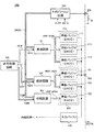
図1に示すように、半導体チップ300は複数のバンク(Bank)310を有し、その周辺にデータ入出力回路領域320が設けられ、バンク310間の領域には、デコーダYDEC及びセンスアンプAMP等が配置されている。また、各バンク310には、複数のメモリセル、例えば、DRAMセルが配置されている。更に、バンク310周辺に配置されたデータ入出力回路領域320には、本発明に係るデータ入出力回路が複数個配列されている。
As shown in FIG. 1, the
次に、図2を参照して、本発明の実施形態に係る半導体装置10の全体回路構成を説明する。
Next, an overall circuit configuration of the
図2に示された半導体装置10は、DDR型のSDRAMであり、外部パッドとして、クロックパッド11a,11b、コマンドパッド12a〜12e、アドレスパッド13、データ入出力パッド(出力パッド)DQ、キャリブレーションパッドZQ及び電源パッドVDDQ,VSSQを備えている。その他、データストローブパッドやリセットパッドなども備えられているが、これらについては図示を省略してある。
The
クロックパッド11a,11bは、それぞれ外部クロック信号CK,/CKが供給されるパッドであり、供給された外部クロック信号CK,/CKは、クロック入力回路21に供給される。尚、信号名の先頭に「/」が付されている信号は、対応する信号の反転信号又はローアクティブな信号であることを意味する。したがって、外部クロック信号CK,/CKは互いに相補の信号である。クロック入力回路21は、外部クロック信号CK,/CKに基づいて単相の内部クロック信号PreCLKを生成し、これをDLL回路80に供給する。DLL回路80は、内部クロック信号PreCLKに基づいて、位相制御された内部クロックLCLKを生成し、データ入出力回路100に供給する。
The clock pads 11 a and 11 b are pads to which external clock signals CK and / CK are respectively supplied. The supplied external clock signals CK and / CK are supplied to the
コマンドパッド12a〜12eは、それぞれロウアドレスストローブ信号/RAS、カラムアドレスストローブ信号/CAS、ライトイネーブル信号/WE、チップセレクト信号/CS、及びオンダイターミネーション信号ODTが供給されるパッドである。これらのコマンド信号CMDは、コマンド入力回路31に供給される。コマンド入力回路31に供給されたこれらコマンド信号CMDは、コマンドデコーダ32に供給される。コマンドデコーダ32は、コマンド信号の保持、デコード及びカウントなどを行うことによって、各種内部コマンドICMDを生成する回路である。生成された内部コマンドICMDは、ロウ系制御回路51、カラム系制御回路52及びモードレジスタ53に供給される。
The
アドレスパッド13は、アドレス信号ADDが供給されるパッドであり、供給されたアドレス信号ADDは、アドレス入力回路41に供給される。アドレス入力回路41の出力は、アドレスラッチ回路42に供給される。アドレスラッチ回路42にラッチされたアドレス信号ADDのうち、ロウアドレスについてはロウ系制御回路51に供給され、カラムアドレスについてはカラム系制御回路52に供給される。また、モードレジスタセットにエントリしている場合には、アドレス信号ADDはモードレジスタ53に供給され、これによってモードレジスタ53の内容が更新される。
The
ロウ系制御回路51の出力は、ロウデコーダ61に供給される。ロウデコーダ61は、メモリセルアレイ70に含まれるいずれかのワード線WLを選択する回路である。メモリセルアレイ70内においては、複数のワード線WLと複数のビット線BLが交差しており、その交点にはメモリセルMCが配置されている(図2では、1本のワード線WL、1本のビット線BL及び1個のメモリセルMCのみを示している)。ビット線BLは、センス回路63内の対応するセンスアンプSAに接続されている。
The output of the
また、カラム系制御回路52の出力は、カラムデコーダ62に供給される。カラムデコーダ62は、センス回路63に含まれるいずれかのセンスアンプSAを選択する回路である。カラムデコーダ62によって選択されたセンスアンプSAは、データアンプ64に接続される。データアンプ64は、リード動作時においてはセンスアンプSAによって増幅されたリードデータRDをさらに増幅し、リードライトバスRWBSを介してこれをデータ入出力回路100に供給する。一方、ライト動作時においては、リードライトバスRWBSを介してデータ入出力回路100から供給されるライトデータを増幅し、これをセンスアンプSAに供給する。
The output of the column control circuit 52 is supplied to the
データ入出力パッドDQは、リードデータの出力及びライトデータの入力を行うためのパッドであり、データ入出力回路100に接続されている。
The data input / output pad DQ is a pad for outputting read data and inputting write data, and is connected to the data input /
図2に示すように、データ入出力回路100には、複数の回路ユニット(以下では、単位バッファと呼ぶ)が含まれている。また、データ入出力回路100はキャリブレーションパッドZQにも接続されており、内部コマンドICMDがキャリブレーション動作を指示している場合には、キャリブレーションパッドZQに接続された外部抵抗Rを用いてキャリブレーション動作が行われる。キャリブレーション動作によって得られたインピーダンスコードは、複数の単位バッファ(即ち、回路ユニット)に対して共通に設定される。
As shown in FIG. 2, the data input /
尚、図2にはデータ入出力パッドDQを簡略化のために1つだけ示しているが、データ入出力パッドDQは通常、複数個設けられている。データ入出力パッドDQを複数個設ける場合には、データ入出力回路100をデータ入出力パッドDQと同数設ける必要がある。
In FIG. 2, only one data input / output pad DQ is shown for simplicity, but a plurality of data input / output pads DQ are usually provided. When providing a plurality of data input / output pads DQ, it is necessary to provide the same number of data input /
図3を参照すると、本発明の実施形態に係る半導体装置10におけるデータ入出力回路100が示されている。図3に示されたデータ入出力回路100は、単一のデータ入出力パッドDQに接続された第1の出力バッファ110及び第2の出力バッファ120と、キャリブレーション用パッドZQに接続されたキャリブレーション回路130と、データ入出力パッドDQに接続された入力バッファ170とを備えている。更に、図3に示されたデータ入出力回路100は、出力制御回路150及び前段回路161〜163を備え、前段回路161〜163は、出力制御回路150から出力される制御信号151P,151N;152P,152N;及び153P,153N及びキャリブレーション回路130からのインピーダンス制御信号DRZQを受けて、リード動作、ライト動作、及び、ODT動作を行なう。
FIG. 3 shows a data input /
即ち、図示されたデータ入出力回路100は、通常のデータ入出力機能の他、ODT機能を有している。ここで、ODT機能とは、データパッドDQに接続された外部バス上で他の半導体装置がデータ転送を行っている場合に、データ入出力回路100を終端抵抗として機能させることによって信号の反射を防止する機能である。
That is, the illustrated data input /
図示されたデータ入出力回路100では、データ出力時(リード動作時)には第1の出力バッファ110と第2の出力バッファ120の両方が活性化され、ODT動作時は第2の出力バッファ120のみが活性化される。つまり、ODT動作時には第1の出力バッファ110は非活性化される。尚、入力バッファ170は、データ入力時(ライト動作時)に活性化される回路であるが、入力バッファ170の構成やデータ入力動作の詳細は、本発明の要旨と直接関係がないため、本明細書での説明は省略する。
In the illustrated data input /
図3に示された第1の出力バッファ110は並列接続された3つの単位バッファ(即ち、回路ユニット)111〜113によって構成され、第2の出力バッファ110も並列接続された3つの単位バッファ(回路ユニット)121〜123によって構成されている。ここで、単位バッファは、切り替えるべき出力インピーダンスの数に応じて設けられ、図示された例では、出力インピーダンスを6段階に切り替えることができる。また、出力インピーダンスを7段階に切り替える必要がある場合には、7つの単位バッファが設置される。
The
図示された単位バッファ111〜113,121〜123は互いに同一の回路構成を有しており、一例として、本実施形態ではいずれも240Ω(調整後の値)のインピーダンスを有している。したがって、全ての単位バッファ111〜113,121〜123が活性化されれば、データピンDQからみた出力回路100の出力インピーダンスは40Ω(=240Ω/6)となる。また、第2の出力バッファ110を構成する3つの単位バッファ121〜123のうち、2つの単位バッファ121,122のみが活性化されれば、データピンDQからみたデータ入出力回路100の出力インピーダンスは120Ω(=240Ω/2)となり、1つの単位バッファ123のみが活性化されれば、データピンDQからみたデータ入出力回路100の出力インピーダンスは240Ωとなる。
The illustrated unit buffers 111 to 113 and 121 to 123 have the same circuit configuration. For example, in this embodiment, all of the unit buffers 111 to 113 and 121 to 123 have an impedance of 240Ω (adjusted value). Therefore, if all the unit buffers 111 to 113 and 121 to 123 are activated, the output impedance of the
単位バッファ111〜113の動作は、前段回路161より供給される動作信号161P,161Nによって制御され、単位バッファ121,122の動作は、前段回路162より供給される動作信号162P,162Nによって制御され、単位バッファ123の動作は、前段回路163より供給される動作信号163P,163Nによって制御される。
The operations of the unit buffers 111 to 113 are controlled by
次に、本発明の理解を容易にするために、図4を参照して、データ入出力回路400の一般的な等価回路例を説明する。図4では、データ入出力回路400のデータ出力回路部分だけが示されており、図示されたデータ出力回路部分は、7つの単位バッファ(ここでは、第1〜第7の単位バッファと呼ぶ)411〜417を含み、各単位バッファ411〜417はここではデータ入出力パッドDQに接続されている。
Next, in order to facilitate understanding of the present invention, a general equivalent circuit example of the data input /
ここで、第1〜第7の単位バッファ411〜417を構成する各単位バッファ(即ち、回路ユニット)は、Pチャネルトランジスタ群Pch、Nチャネルトランジスタ群Nch、及びP及びNチャネルトランジスタ群Pch,Nch間に直列に接続された2つの抵抗Rを備え、2つの抵抗Rの共通接続点はデータ入出力パッドDQに接続されている。実際に使用される場合、Pチャネルトランジスタ群Pchのソースは電源VDDに接続され、Nチャネルトランジスタ群Nchのソースは電源(接地電源)VSSに接続されている。 Here, each unit buffer (that is, circuit unit) constituting the first to seventh unit buffers 411 to 417 includes a P-channel transistor group Pch, an N-channel transistor group Nch, and P and N-channel transistor groups Pch and Nch. Two resistors R connected in series are provided, and a common connection point of the two resistors R is connected to the data input / output pad DQ. When actually used, the source of the P-channel transistor group Pch is connected to the power supply VDD, and the source of the N-channel transistor group Nch is connected to the power supply (ground power supply) VSS.
図示されたPチャネルトランジスタ群Pch及びNチャネルトランジスタ群Nchはそれぞれ複数のP及びNチャネルトランジスタ(例えば、5個のトランジスタ)によって構成され、これら複数のP及びNチャネルトランジスタを選択的に動作させることによって、外部に接続されるべき回路とのマッチングを取ることができる。この場合、Pチャネルトランジスタ群Pchの5個のPchトランジスタはプルアップ回路PUを構成し、他方、Nチャネルトランジスタ群Nchの5個のNchトランジスタはプルダウン回路PDを構成する。 The illustrated P channel transistor group Pch and N channel transistor group Nch are each composed of a plurality of P and N channel transistors (for example, five transistors), and selectively operate the plurality of P and N channel transistors. Thus, matching with a circuit to be connected to the outside can be achieved. In this case, the five Pch transistors of the P channel transistor group Pch constitute a pull-up circuit PU, while the five Nch transistors of the N channel transistor group Nch constitute a pull-down circuit PD.
しかしながら、各P及びNチャネルトランジスタ群Pch,Nchを構成するトランジスタの動作は本発明と直接には関係していないので、図4では、各単位バッファの複数のトランジスタを単一のトランジスタによって表している。 However, since the operations of the transistors constituting each P and N channel transistor group Pch, Nch are not directly related to the present invention, in FIG. 4, a plurality of transistors in each unit buffer are represented by a single transistor. Yes.
また、図示された単位バッファは、単位バッファに含まれるプルアップ回路PU又はプルダウン回路PDをオンにすることにより、抵抗Rを終端抵抗として使用したODT機能を有している。このため、抵抗RはODT抵抗と呼ぶことができる。ODT抵抗Rを配置することによって、図4に示されたデータ入出力回路100は、単位バッファに接続された内部回路の非選択状態において外部回路からの信号に対する終端回路を構成することができる。通常、各単位バッファ411〜417に設けられる抵抗Rの抵抗値は、各単位バッファの出力インピーダンスと等しい値、例えば、240Ωに設計されている。
The illustrated unit buffer has an ODT function using the resistor R as a termination resistor by turning on the pull-up circuit PU or the pull-down circuit PD included in the unit buffer. For this reason, the resistor R can be called an ODT resistor. By arranging the ODT resistor R, the data input /
図4に示されたデータ入出力回路400の単位バッファ411〜417中のトランジスタは、静電気放電(ESD)に対してある程度保護素子としても機能する。しかしながら、図示されたデータ入出力回路400においても、外部からの静電気放電(ESD)に対する保護回路を設けることが望ましい。
The transistors in the unit buffers 411 to 417 of the data input /
そこで、本発明者等は、ESD保護回路の最適位置を決定するために、種々の実験を行なった。 Therefore, the present inventors conducted various experiments in order to determine the optimum position of the ESD protection circuit.
図5を参照すると、実験に用いられた回路の一例が示されている。図5では、パッド500に対して、図4と同様に、それぞれODT抵抗を有する7つの単位バッファを設けた例が示されている。図示されたパッド500は、100μm×50μm程度の長辺及び短辺を備えた矩形形状を有している。一方、図示された7つの単位バッファは、それぞれPチャネルトランジスタ群中の単一の出力トランジスタ(出力Tr)501〜507によって示されており、他の部分は省略されている。
Referring to FIG. 5, an example of a circuit used in the experiment is shown. FIG. 5 shows an example in which seven unit buffers each having an ODT resistance are provided for the
また、図5では、第1の配線部分511〜517及びODT抵抗を構成する第2の配線部分521〜527が示されている。第1の配線部分511〜517及はアルミニウムによって形成され、他方、第2の配線部分521〜527は抵抗Rの抵抗値を実現するためにタングステンによって形成され、第1の配線部分511〜517に直列に接続されている。
FIG. 5 also shows the
第1の配線部分511〜517は、例えば、Pチャンネルトランジスタによって構成された出力トランジスタ(出力Tr)501〜507のドレイン領域に接続されている。図示された各出力トランジスタ(出力Tr)501〜507は、第1の配線部分511〜517の両側に配置されたゲート電極と、各ゲート領域に関連した拡散領域とによって特徴付けられている。したがって、図5に示された第1及び第2の配線部分511〜517及び521〜527は、図4に示されたPチャネルトランジスタPchのドレインから抵抗Rまでの経路に相当していることが分る。
The
図5を更に参照すると、第3の配線部分531が設けられており、当該第3の配線部分531は第2の配線部分521〜527に共通に接続され、第3の配線部分531は第4の配線部分541〜547を介して、データ入出力パッド501の長辺に接続されている。
With further reference to FIG. 5, a
ここで,第4の配線部分541〜547は、パッド500に隣接して設けられたESD保護回路を構成する7つのトランジスタに接続されている。即ち、図5では、各単位バッファのODT抵抗とパッド500とが、共通接続配線経路及び第4の配線部分541〜547を介して接続されている。ESD保護回路を構成するトランジスタは出力トランジスタ501〜507よりも大きなサイズを有している。
Here, the
このように、第3の配線部分531により、複数の単位ユニットからの第2の配線部分521〜527を共通に接続した場合、ESDに対して十分な耐圧を維持できるものの、単位バッファの数が増加すると、第3の配線部分531における抵抗の影響を受け、出力抵抗の精度が悪くなることが判明した。
As described above, when the second wiring portions 521 to 527 from a plurality of unit units are connected in common by the
図6を参照すると、本発明者等の他の実験によるESD保護回路の配置例が示されている。ここでは、正方形形状のパッド600の一辺に、図5と同様な形式で表された出力トランジスタ(出力Tr)601〜607、各出力トランジスタ601〜607に接続された第1の配線部分611〜617、及びタングステンによって形成され、一端を第1の配線部分611〜617にそれぞれ接続された第2の配線部分621〜627とを備え、第2の配線部分621〜627の他端を直接正方形形状のパッド600に接続している。
Referring to FIG. 6, an arrangement example of an ESD protection circuit according to another experiment of the present inventors is shown. Here, on one side of the
また、図示された例では、パッド600の他の辺に隣接してESD保護回路が設けられ、ESD保護回路を構成する各トランジスタに接続された第3の配線部分631〜637がパッド600の他の辺に接続されている。
Further, in the illustrated example, an ESD protection circuit is provided adjacent to the other side of the
図6に示された構成では、図5に示された構成に比較してODT抵抗の抵抗値の誤差を少なくできる反面、ESD耐圧が低いことが判明した。 In the configuration shown in FIG. 6, it is found that the ESD withstand voltage is low while the error of the resistance value of the ODT resistor can be reduced as compared with the configuration shown in FIG.
図7を参照すると、本発明を原理的に説明するデータ入出力回路のレイアウトが示されており、ここでは、図5及び6と同様に、データ入出力回路の出力回路部のレイアウトのみが示されている。この関係で、以下の説明は、データ入出力パッドDQ700に関連した回路についてのみ説明するが、本発明は何等これに限定されることなく、他のパッドに関連した回路にも同様に適用できる。 Referring to FIG. 7, there is shown a layout of a data input / output circuit for explaining the principle of the present invention. Here, as in FIGS. 5 and 6, only the layout of the output circuit portion of the data input / output circuit is shown. Has been. In this connection, the following description will be given only for a circuit related to the data input / output pad DQ700, but the present invention is not limited to this, and can be similarly applied to circuits related to other pads.
図7に示された出力回路部は、出力トランジスタ(出力Tr)(例えば、Pchトランジスタ)701〜707、ODT抵抗部、及びESD保護回路(ESD)を備え、図からも明らかな通り、ESD保護回路(ESD)はODT抵抗部とパッドDQ700の間に設けられている。出力トランジスタ701〜707の例えばドレインに接続され、アルミニウムによって形成された第1の配線部711〜717は、タングステンによって形成された第2の配線部721〜727にそれぞれ直列に接続されている。第1の配線部711〜717の一部と、これら第1の配線部711〜717にそれぞれ直列の接続された第2の配線部721〜727はODT抵抗部として動作する。
The output circuit unit shown in FIG. 7 includes output transistors (output Tr) (for example, Pch transistors) 701 to 707, an ODT resistor unit, and an ESD protection circuit (ESD). The circuit (ESD) is provided between the ODT resistor and the pad DQ700.
更に、第2の配線部721〜727は、アルミニウムによって形成された第3の配線部731〜737に直列に接続され、これら第3の配線部731〜737はそれぞれパッド700に個別に接続されている。第3の配線部731〜737は、矩形形状のパッド700の長辺に接続され、且つ、ESD保護回路を構成するトランジスタ741〜747に接続されている。
Further, the
図7からも明らかなように、第1〜第3の配線部によって構成される出力トランジスタ701〜707からパッド700に至る配線は、個別独立している。即ち、複数(図7では7個)の単位バッファは、ESD保護回路用第3の配線部731〜737をそれぞれ含んだ構成を有している。このように、単位バッファを繰り返し配置した構成を有しているため、ESDに対して均一な放電経路を形成することができる。したがって、図5と同程度のESD耐圧を実現でき、また、ESDに対する抵抗値も図6と同程度に均一化することができる。
As is clear from FIG. 7, the wiring from the
図8を参照すると、図7に示したデータ入出力回路の等価回路図が示されている。尚、図8では、単位バッファを構成するPchトランジスタ701〜707だけでなく、Nchトランジスタ751〜757及びこれらNchトランジスタ751〜757に接続されたODT抵抗761〜767も示されている。
Referring to FIG. 8, there is shown an equivalent circuit diagram of the data input / output circuit shown in FIG. In FIG. 8, not only the
図示されたESD保護回路は、抵抗721〜727と抵抗761〜767の共通接続点にそれぞれドレインを接続されたNchトランジスタ741〜747を備え、各Nchトランジスタ741〜747のドレインはパッド700に個別に接続されている。また、ESD保護回路を構成する各Nchトランジスタ741〜747のゲートとソースは共通に接続され、電源(設置電源)VSSパッドに接続されている。
The illustrated ESD protection circuit includes
図8に示されたデータ入出力回路は、独立した7つの配線経路を有しているため、7つの段階の出力インピーダンスを確実に実現することができる。例えば、単一の単位バッファに伴う寄生抵抗が1Ωである場合、単一の単位バッファだけが使用される場合における寄生抵抗の影響は1Ωとなり、7つの単位バッファが使用される場合における寄生抵抗の影響は1/7Ωとなる。このため、出力抵抗を容易に所望に値に適合させることができる。 Since the data input / output circuit shown in FIG. 8 has seven independent wiring paths, seven stages of output impedance can be reliably realized. For example, when the parasitic resistance associated with a single unit buffer is 1Ω, the influence of the parasitic resistance when only a single unit buffer is used is 1Ω, and the parasitic resistance when seven unit buffers are used The effect is 1 / 7Ω. For this reason, the output resistance can be easily adjusted to a desired value.
ここで、図7の第1の配線部711〜717と第2の配線部721〜727とを直列に接続した場合における各直列回路の抵抗値を239Ωとし、ESD保護回路の寄生抵抗を1Ωであるものとする。この状態で、単一の単位バッファだけが使用される場合、直列抵抗は240Ωとなり、他方、7個の単位バッファが使用される場合には、240/7(=34.29Ω)となる。よって、ESD保護回路を設けたことによる寄生抵抗の影響を実質的に無くすことができる。
Here, when the
図9を参照すると、本発明の第1の実施形態に係るデータ入出力回路のレイアウトが示されている。図9に示されたデータ入出力回路のレイアウトは、図8に示された等価回路に対応している。ここでは、図8との対応関係を明確にするために、図10(a)及び(b)に示された回路図及び実体配線図をも参照して説明する。 FIG. 9 shows a layout of the data input / output circuit according to the first embodiment of the present invention. The layout of the data input / output circuit shown in FIG. 9 corresponds to the equivalent circuit shown in FIG. Here, in order to clarify the correspondence with FIG. 8, the description will be made with reference to the circuit diagrams and the actual wiring diagrams shown in FIGS. 10 (a) and 10 (b).
図10(a)及び(b)では、理解を容易にするために図9の右端に示された単位ユニットのみが示され、図10(a)及び(b)における各部の位置は互いに対応付けられている。図10(b)に示されているように、P型基板1001に形成されたNウェル1002に、2つのP型拡散層が設けられ、Pchトランジスタのソース、ドレインが形成され、ソース、ドレイン間のチャネル領域にはゲート電極が形成されている。また、P型基板1001には、N型拡散層が形成され、Nchトランジスタ757のドレイン、ソースが設けられ、ドレイン、ソース間のチャネル領域にはゲート電極が形成されている。
10 (a) and 10 (b), only the unit unit shown at the right end of FIG. 9 is shown for easy understanding, and the position of each part in FIGS. 10 (a) and 10 (b) is associated with each other. It has been. As shown in FIG. 10B, two P-type diffusion layers are provided in an N well 1002 formed on a P-
また、図示された例では、Nchトランジスタによって形成されたESD保護回路を形成するNchトランジスタ747が設けられている。当該Nchトランジスタ747のソースとゲートは、図10(a)に示すように共通に接続され、電源(例えば、接地電源)に接続され、抵抗を構成している。
In the illustrated example, an
図10(b)に示されているように、Pchトランジスタ707のドレインは、基板1001上に形成された絶縁膜に設けられたコンタクトを通して、抵抗Rに接続されており、Nchトランジスタのドレインもコンタクトを介して、抵抗Rに接続されている。2つの抵抗Rは共通接続領域1004を介して、外部配線1005に接続され、当該外部配線1005はパッド700に接続されている。図10(b)に示された外部配線1005は、図9に示されたESD保護回路を構成するトランジスタ747上の配線737を含んでいる。
As shown in FIG. 10B, the drain of the
図9に示されたデータ入出力回路は、図10に示されたPchトランジスタ707、Nchトランジスタ757、ODT抵抗Rを形成する抵抗Rの一部、及び外部配線1005によって表されている。この関係で、図9では、共通接続領域1004及び内部配線等は省略されている。
The data input / output circuit shown in FIG. 9 is represented by the
各単位バッファの出力トランジスタ(出力Tr)からパッド700までの抵抗値は、互いに同一であり、且つ、各単位バッファは同一のESD経路を形成できる。即ち、図9に示されたデータ入出力回路は高精度な抵抗値を得ることができると共に、十分なESD耐圧を実現できる。
The resistance values from the output transistor (output Tr) of each unit buffer to the
図11を参照して、本発明の第2の実施形態に係るデータ入出力回路を説明するが、図11においても、データ出力回路のみが示されている。図11では、図9及び10と同様な形式で表されたPchトランジスタ1103及びNchトランジスタ1105、ODT抵抗を備えている。尚、図11では、各単位バッファは同一の形状であるため、最左端の単位バッファのみに参照番号が付されている。
The data input / output circuit according to the second embodiment of the present invention will be described with reference to FIG. 11, but only the data output circuit is shown in FIG. 11 includes a
図11に示されたデータ入出力回路は、ODT抵抗に直列に接続され、且つ、ESD保護回路のトランジスタ747のドレインに接続された配線1107によって特徴付けられている。即ち、図11に示された配線1107は、2つに分岐された分岐配線を構成しており、各分岐配線1107には、ESD保護回路を構成するトランジスタのドレインに接続されると共に、パッド1100にも接続されている。
The data input / output circuit shown in FIG. 11 is characterized by a
このように、ESD保護回路上の配線1107を複数に分岐し、並列に接続された分岐配線を構成することによっても、図9と同様な効果を得ることができる。また、ESD保護回路の配線1107を並列な分岐配線し、各分岐配線をトランジスタに接続することにより、放電経路を増加させてESD耐圧を上げることができ、且つ、放電電荷のアンバランスを軽減できる。
As described above, the same effect as that of FIG. 9 can also be obtained by branching the
図12を参照して、本発明の第3の実施形態に係るデータ入出力回路のレイアウトを説明する。図12では、パッド1200に接続されるべき出力トランジスタ(出力Tr)が7個であり、ESDの放電経路を形成するESD保護回路のトランジスタが9個の場合を示している。即ち,ESD保護回路のトランジスタの数が出力トランジスタTrの数よりも多い場合を示している。このように,ESD保護回路のトランジスタの数が出力トランジスタTrの数よりも多い場合、放電経路の数が多いため、ESD保護の点で問題ないように考えられる。
The layout of the data input / output circuit according to the third embodiment of the present invention will be described with reference to FIG. FIG. 12 shows a case where there are seven output transistors (output Tr) to be connected to the
しかしながら、実際には、ESD保護回路のトランジスタのトランジスタが出力トランジスタTrよりも多くなると、ESDの放電経路に差ができてしまい、電流が集中してしまう放電経路が出来てしまい、結果的にESD破壊が生じることがあった。 However, in reality, when the number of transistors of the ESD protection circuit is larger than that of the output transistor Tr, a difference occurs in the ESD discharge path, and a discharge path in which current is concentrated is formed. Destruction sometimes occurred.
図12では、このことを考慮して、7つの単位バッファ1211〜1217の外に、ESD回路を構成する2つの付加ESD保護回路1221、1223に、出力ダミートランジスタ回路1225、1227が接続されている。このように、付加ESD保護回路1221、1223と出力ダミートランジスタ回路1225、1227を含む出力ダミー回路1229は、それぞれ単位バッファ1211、1217と同一であるため、ESDに対する放電経路を均一にすることができる。このため、ESDによる破壊を防止することができる。即ち、図12に示されたデータ入出力回路は出力トランジスタTrを追加して、単位バッファと同様な構成をとることにより、ESDによる破壊を防止できる。
In FIG. 12, in consideration of this, the output
図13を参照して、本発明の第4の実施形態に係るデータ入出力回路のレイアウトを説明する。図13に示された例では、パッド1300に接続されるべき出力トランジスタTrが7個であり、ESD保護回路が出力トランジスタTrの数よりも少ない場合(図13では、ESD保護回路を構成する回路の数が5個の場合が示されている)、ESD保護回路を備えていない出力トランジスタTr回路1301、1303にも、追加的なESD保護回路1305、1307がそれぞれ接続されている。ここで、出力トランジスタTr回路1301、1303は、他の単位バッファにおける出力トランジスタ回路Trと同様に、Pchトランジスタ及びNchトランジスタ、及びODT抵抗を含んでいる。
The layout of the data input / output circuit according to the fourth embodiment of the present invention will be described with reference to FIG. In the example shown in FIG. 13, the number of output transistors Tr to be connected to the
この構成によっても、ESD放電経路が同一となり、この結果、ESD放電経路を均一化でき、ESD破壊を防止できる。 Also with this configuration, the ESD discharge path is the same, and as a result, the ESD discharge path can be made uniform and ESD breakdown can be prevented.
以上説明した実施形態では、データ入出力パッドDQに接続されたデータ入出力回路についてのみ説明したが、本発明は何等これに限定されることなく、データ以外の信号を入出力するパッドに接続された単位バッファ以外の回路ユニットにも同様に適用できる。更に、データ入出力パッドを備えたDRAMについて説明したが、本発明はDRAM以外の半導体装置にも同様に適用できる。 In the embodiment described above, only the data input / output circuit connected to the data input / output pad DQ has been described. However, the present invention is not limited to this and is connected to a pad for inputting / outputting signals other than data. The same applies to circuit units other than the unit buffer. Furthermore, although a DRAM having a data input / output pad has been described, the present invention can be similarly applied to a semiconductor device other than a DRAM.
300 半導体チップ300
310 バンク(Bank)
320 データ入出力回路領域
21 クロック入力回路
31 コマンド入力回路
32 コマンドデコーダ
41 アドレス入力回路
42 アドレスラッチ回路
51 ロウ系制御回路
52 カラム系制御回路
53 モードレジスタ
61 ロウデコーダ
62 カラムデコーダ
63 センス回路
64 データアンプ
70 メモリセルアレイ
80 DLL回路
100 データ入出力回路
110 第1の出力バッファ
111〜113 単位バッファ
120 第2の出力バッファ
121〜123 単位バッファ
130 キャリブレーション回路
150 出力制御回路
161〜163 前段回路
170 入力バッファ
411〜417 第1〜第7の単位バッファ
500、600 パッド
501〜507 出力トランジスタ
511〜517 第1の配線部分
521〜527 第2の配線部分
531 第3の配線部分
541〜547 第4の配線部分
601〜607 出力トランジスタ
611〜617 第1の配線部分
621〜627 第2の配線部分
631〜637 第3の配線部分
700 パッド
701〜707 出力トランジスタ(Pch)
711〜717 第1の配線部
721〜727 第2の配線部
731〜737 第3の配線部
741〜747 トランジスタ(Nch)
751〜757 トランジスタ(Nch)
1001 半導体基板(P型)
1002 Nウェル
1004 共通接続領域
1005 外部配線
1100 パッド
1103 トランジスタ(Pch)
1105 トランジスタ(Nch)
1107 分岐配線
1200 パッド
1211〜1217 単位バッファ
1221、1223 付加ESD保護回路
1225、1227 出力ダミートランジスタ回路
1229 出力ダミー回路
1300 パッド
1301、1303 出力トランジスタ回路
1305、1307 追加的なESD保護回路
300
310 Bank
320 Data Input /
711-717 1st wiring part 721-727 2nd wiring part 731-737 3rd wiring part 741-747 Transistor (Nch)
751-757 transistor (Nch)
1001 Semiconductor substrate (P type)
1002 N well 1004
1105 Transistor (Nch)
1107
Claims (14)
前記各回路ユニットは、トランジスタ回路、当該トランジスタ回路に隣接配置された終端抵抗調整(ODT)回路、静電気放電(ESD)保護回路、及び、前記トランジスタ回路、前記ODT回路、及び前記ESD保護回路を通して延在し、前記パッドに接続された配線を含み、
前記複数の回路ユニットの前記配線は、互いに分離して個別に前記パッドに接続されていることを特徴とする半導体装置。 A pad and a plurality of circuit units arranged adjacent to the pad;
Each circuit unit extends through a transistor circuit, a termination resistance adjustment (ODT) circuit adjacent to the transistor circuit, an electrostatic discharge (ESD) protection circuit, and the transistor circuit, the ODT circuit, and the ESD protection circuit. Including a wire connected to the pad;
The semiconductor device according to claim 1, wherein the wirings of the plurality of circuit units are separated from each other and individually connected to the pad.
Priority Applications (1)
| Application Number | Priority Date | Filing Date | Title |
|---|---|---|---|
| JP2013013045A JP2014146641A (en) | 2013-01-28 | 2013-01-28 | Semiconductor device |
Applications Claiming Priority (1)
| Application Number | Priority Date | Filing Date | Title |
|---|---|---|---|
| JP2013013045A JP2014146641A (en) | 2013-01-28 | 2013-01-28 | Semiconductor device |
Publications (1)
| Publication Number | Publication Date |
|---|---|
| JP2014146641A true JP2014146641A (en) | 2014-08-14 |
Family
ID=51426672
Family Applications (1)
| Application Number | Title | Priority Date | Filing Date |
|---|---|---|---|
| JP2013013045A Pending JP2014146641A (en) | 2013-01-28 | 2013-01-28 | Semiconductor device |
Country Status (1)
| Country | Link |
|---|---|
| JP (1) | JP2014146641A (en) |
Cited By (2)
| Publication number | Priority date | Publication date | Assignee | Title |
|---|---|---|---|---|
| US10586599B1 (en) | 2018-12-21 | 2020-03-10 | Toshiba Memory Corporation | Semiconductor storage device |
| US11456595B2 (en) | 2020-09-25 | 2022-09-27 | Samsung Electronics Co., Ltd. | Electrostatic protection circuit and semiconductor device including the same |
-
2013
- 2013-01-28 JP JP2013013045A patent/JP2014146641A/en active Pending
Cited By (2)
| Publication number | Priority date | Publication date | Assignee | Title |
|---|---|---|---|---|
| US10586599B1 (en) | 2018-12-21 | 2020-03-10 | Toshiba Memory Corporation | Semiconductor storage device |
| US11456595B2 (en) | 2020-09-25 | 2022-09-27 | Samsung Electronics Co., Ltd. | Electrostatic protection circuit and semiconductor device including the same |
Similar Documents
| Publication | Publication Date | Title |
|---|---|---|
| US10014037B2 (en) | Semiconductor memory package including memory device with inverting circuit | |
| JP5490482B2 (en) | Semiconductor device | |
| US8693264B2 (en) | Memory device having sensing circuitry with automatic latching of sense amplifier output node | |
| US9704561B2 (en) | Device having multiple switching buffers for data paths controlled based on IO configuration modes | |
| US10156893B1 (en) | Wiring with external terminal | |
| US9754666B2 (en) | Resistive ratio-based memory cell | |
| US20150365077A1 (en) | Semiconductor Device Having Output Buffers and Voltage Path Coupled to Output Buffers | |
| US20200075083A1 (en) | Dram sense amplifier active matching fill features for gap equivalence systems and methods | |
| US8674411B2 (en) | Semiconductor device employing circuit blocks having the same characteristics | |
| JP2014146641A (en) | Semiconductor device | |
| US10916294B2 (en) | Apparatuses and methods for concentrated arrangement of amplifiers | |
| US20230205712A1 (en) | Memory devices with multiple pseudo-channels | |
| WO2014103735A1 (en) | Semiconductor device | |
| US11296047B2 (en) | Wiring with external terminal | |
| JP5710955B2 (en) | Semiconductor device | |
| US9336856B2 (en) | Device and apparatus having address and command input paths | |
| US8717795B2 (en) | Semiconductor device having plural circuit blocks operating at the same timing | |
| US20060152965A1 (en) | Memory with reduced bitline leakage current and method for the same | |
| CN112309442B (en) | Device comprising conductive structures and layout therefor | |
| JP2015159435A (en) | semiconductor device | |
| WO2014112453A1 (en) | Semiconductor device | |
| JP2014146910A (en) | Semiconductor device | |
| JP2010171331A (en) | Semiconductor device | |
| JP2014143257A (en) | Semiconductor device | |
| JP2014132618A (en) | Semiconductor device |