JP2014075476A - Organic solar cell - Google Patents
Organic solar cell Download PDFInfo
- Publication number
- JP2014075476A JP2014075476A JP2012222105A JP2012222105A JP2014075476A JP 2014075476 A JP2014075476 A JP 2014075476A JP 2012222105 A JP2012222105 A JP 2012222105A JP 2012222105 A JP2012222105 A JP 2012222105A JP 2014075476 A JP2014075476 A JP 2014075476A
- Authority
- JP
- Japan
- Prior art keywords
- layer
- doped
- solar cell
- organic solar
- compound
- Prior art date
- Legal status (The legal status is an assumption and is not a legal conclusion. Google has not performed a legal analysis and makes no representation as to the accuracy of the status listed.)
- Pending
Links
Classifications
-
- Y—GENERAL TAGGING OF NEW TECHNOLOGICAL DEVELOPMENTS; GENERAL TAGGING OF CROSS-SECTIONAL TECHNOLOGIES SPANNING OVER SEVERAL SECTIONS OF THE IPC; TECHNICAL SUBJECTS COVERED BY FORMER USPC CROSS-REFERENCE ART COLLECTIONS [XRACs] AND DIGESTS
- Y02—TECHNOLOGIES OR APPLICATIONS FOR MITIGATION OR ADAPTATION AGAINST CLIMATE CHANGE
- Y02E—REDUCTION OF GREENHOUSE GAS [GHG] EMISSIONS, RELATED TO ENERGY GENERATION, TRANSMISSION OR DISTRIBUTION
- Y02E10/00—Energy generation through renewable energy sources
- Y02E10/50—Photovoltaic [PV] energy
- Y02E10/549—Organic PV cells
Landscapes
- Electroluminescent Light Sources (AREA)
- Photovoltaic Devices (AREA)
Abstract
【課題】励起子の失活、再結合損失を抑制した有機太陽電池を提供する。
【解決手段】陽極、光電変換層及び陰極を含む有機太陽電池であって、前記光電変換層がn型半導体層及び第1のドーパントを含むドープn型半導体層を含み、前記n型半導体層とドープn型半導体層が接している有機太陽電池。
【選択図】なしAn organic solar cell in which exciton deactivation and recombination loss are suppressed is provided.
An organic solar cell including an anode, a photoelectric conversion layer, and a cathode, wherein the photoelectric conversion layer includes an n-type semiconductor layer and a doped n-type semiconductor layer including a first dopant, and the n-type semiconductor layer; An organic solar cell in contact with a doped n-type semiconductor layer.
[Selection figure] None
Description
本発明は、有機太陽電池に関する。 The present invention relates to an organic solar cell.
有機太陽電池(有機薄膜太陽電池)は、光信号を電気信号に変換するフォトダイオードや撮像素子、光エネルギーを電気エネルギーに変換する太陽電池に代表されるように、光入力に対して電気出力を示す装置である。 Organic solar cells (organic thin-film solar cells) provide electrical output with respect to light input, as typified by photodiodes and imaging devices that convert optical signals into electrical signals, and solar cells that convert optical energy into electrical energy. It is a device to show.
太陽電池は、化石燃料の枯渇問題や地球温暖化問題を背景に、クリーンエネルギー源として近年大変注目され、研究開発が盛んに行なわれている。
従来、実用化されてきたのは、単結晶Si、多結晶Si、アモルファスSi等に代表されるシリコン系太陽電池であるが、高価であることや原料Siの不足問題等が表面化するにつれて、次世代太陽電池への要求が高まりつつある。このような背景の中で、有機太陽電池は、安価で毒性が低く、原材料不足の懸念もないことから、シリコン系太陽電池に次ぐ次世代の太陽電池として大変注目を集めている。
In recent years, solar cells have attracted a great deal of attention as a clean energy source against the background of fossil fuel depletion problems and global warming problems, and research and development have been actively conducted.
Conventionally, silicon solar cells represented by single crystal Si, polycrystal Si, amorphous Si, etc. have been put into practical use. However, as the cost and raw material Si shortage problems surface, The demand for next generation solar cells is increasing. Against this background, organic solar cells are attracting much attention as next-generation solar cells next to silicon-based solar cells because they are inexpensive, have low toxicity, and do not have a fear of shortage of raw materials.
有機太陽電池及びそれを用いた有機太陽電池モジュールにおいて、高効率化及び低コスト化が求められている。
有機太陽電池素子では、光照射により生成された励起子から、正孔と電子の両電荷が分離生成される。従って、有機太陽電池における高効率化は、光活性な光電変換層の中での励起子の失活を抑制し、電荷分離を効果的に行うことによって実現することが可能である。
In an organic solar cell and an organic solar cell module using the same, high efficiency and low cost are required.
In the organic solar cell element, both holes and electrons are separated and generated from excitons generated by light irradiation. Therefore, high efficiency in the organic solar cell can be realized by suppressing deactivation of excitons in the photoactive photoelectric conversion layer and effectively performing charge separation.
励起子の再結合を伴わずに励起子拡散を制御することは、有機太陽電池の高効率化において非常に重要である。
励起子の拡散距離は、構造及び化学的な純度に関して完璧な単結晶を用いれば大きくすることができると考えられるが、汎用に単結晶有機材料を使用することは不可能である。
Controlling exciton diffusion without exciton recombination is very important in increasing the efficiency of organic solar cells.
The diffusion distance of excitons can be increased by using a perfect single crystal in terms of structure and chemical purity, but it is impossible to use a single crystal organic material for general purposes.
励起子の拡散距離を長くする代わりに、電荷分離をもたらすpn界面までの平均的な距離を小さくすることが提案されている。i層(p材料とn材料の混合層)やバルクヘテロ構造を導入して、光生成された励起子が非常に短い距離を拡散するだけでpn界面に到達すればよいことになり、変換効率が向上することが見出された。 Instead of increasing the exciton diffusion distance, it has been proposed to reduce the average distance to the pn interface that results in charge separation. By introducing an i layer (mixed layer of p and n materials) or a bulk heterostructure, the photogenerated excitons only have to reach the pn interface by diffusing a very short distance, and the conversion efficiency is improved. It has been found to improve.
また、低分子材料と同様に高分子材料を用いた有機太陽電池においても、p材料として導電性高分子、n材料として可溶性C60誘導体を用いて、それらを混合、熱処理してミクロ相分離を誘起してヘテロ界面を増やすことにより変換効率を向上させる、所謂バルクヘテロ構造の研究が主に行なわれている。 In addition, in organic solar cells using polymer materials as well as low molecular materials, using conductive polymers as p materials and soluble C60 derivatives as n materials, they are mixed and heat-treated for microphase separation. Research on so-called bulk heterostructures, in which conversion efficiency is improved by inducing heterointerfaces by induction, is mainly performed.
また、有機太陽電池の特性を改善する策として、他のアプローチは以下のようなものが挙げられる。
有機太陽電池においてnドーピングを行うことで、変換効率を向上する報告がなされている。
例えば、特許文献1において、有機半導体マトリックス材料へのnドーパントとなる金属錯体として、M2hpp4(MはCr、Mn、Fe、Co、Ni、Cu、Zn、Mo又はWである)で表される金属錯体が報告されている。
As other measures for improving the characteristics of the organic solar cell, other approaches include the following.
There have been reports of improving conversion efficiency by performing n doping in organic solar cells.
For example, in Patent Document 1, a metal complex serving as an n-dopant to an organic semiconductor matrix material is represented by M 2 hpp 4 (M is Cr, Mn, Fe, Co, Ni, Cu, Zn, Mo, or W). Metal complexes have been reported.
非特許文献1において、有機太陽電池素子において、n型半導体として用いるC60層に対して、IrC6錯体をドーピングしたことが報告されている。
特許文献2において、光活性層よりも大きな光学バンドギャップを有する電荷伝導層として、ドーピングにより導電率を向上した層を用いることが報告されている。
In Non-Patent Document 1, in the organic solar cell element, relative to C60 layer used as an n-type semiconductor, it has been reported that doped with IRC 6 complex.
In Patent Document 2, it is reported that a layer whose conductivity is improved by doping is used as a charge conductive layer having an optical band gap larger than that of the photoactive layer.
本発明の目的は、励起子の失活、再結合損失を抑制した有機太陽電池を提供することである。 An object of the present invention is to provide an organic solar cell in which exciton deactivation and recombination loss are suppressed.
本発明によれば、以下の有機太陽電池が提供される。
1.陽極、光電変換層及び陰極を含む有機太陽電池であって、前記光電変換層がn型半導体層及び第1のドーパントを含むドープn型半導体層を含み、前記n型半導体層とドープn型半導体層が接している有機太陽電池。
2.陽極、第1の光電変換層、中間電極、第2の光電変換層及び陰極をこの順に含む有機太陽電池であって、前記第1の光電変換層及び第2の光電変換層のうち少なくとも1つがn型半導体層及び第1のドーパントを含むドープn型半導体層を含み、前記n型半導体層とドープn型半導体層が接している有機太陽電池。
3.前記n型半導体層、前記ドープn型半導体層及び前記陰極がこの順に積層されている1又は2に記載の有機太陽電池。
4.前記第1のドーパントが金属錯体である1〜3のいずれかに記載の有機太陽電池。
5.前記金属錯体がイリジウム(Ir)錯体又はルテニウム(Ru)錯体であり、かつ、イオン化ポテンシャル(Ip)が5.7eVよりも小さい4に記載の有機太陽電池。
6.前記第1のドーパントの三重項エネルギーギャップが、前記n型半導体層に含まれるn型半導体材料の三重項エネルギーギャップよりも大きい1〜5のいずれかに記載の有機太陽電池。
7.前記ドープn型半導体層に含まれるn型半導体材料がフラーレン又はフラーレン誘導体である1〜6のいずれかに記載の有機太陽電池。
8.前記光電変換層、又は前記第1の光電変換層及び第2の光電変換層のうち少なくとも1つが、p型半導体層及び第2のドーパントを含むドープp型半導体層を含む1〜7のいずれかに記載の有機太陽電池。
According to the present invention, the following organic solar cell is provided.
1. An organic solar cell including an anode, a photoelectric conversion layer, and a cathode, wherein the photoelectric conversion layer includes an n-type semiconductor layer and a doped n-type semiconductor layer including a first dopant, and the n-type semiconductor layer and the doped n-type semiconductor Organic solar cells with layers in contact.
2. An organic solar cell including an anode, a first photoelectric conversion layer, an intermediate electrode, a second photoelectric conversion layer, and a cathode in this order, at least one of the first photoelectric conversion layer and the second photoelectric conversion layer being An organic solar cell comprising an n-type semiconductor layer and a doped n-type semiconductor layer containing a first dopant, wherein the n-type semiconductor layer is in contact with the doped n-type semiconductor layer.
3. 3. The organic solar battery according to 1 or 2, wherein the n-type semiconductor layer, the doped n-type semiconductor layer, and the cathode are stacked in this order.
4). The organic solar battery according to any one of 1 to 3, wherein the first dopant is a metal complex.
5. 5. The organic solar cell according to 4, wherein the metal complex is an iridium (Ir) complex or a ruthenium (Ru) complex, and the ionization potential (Ip) is smaller than 5.7 eV.
6). The organic solar cell according to any one of 1 to 5, wherein a triplet energy gap of the first dopant is larger than a triplet energy gap of an n-type semiconductor material included in the n-type semiconductor layer.
7). The organic solar cell according to any one of 1 to 6, wherein the n-type semiconductor material contained in the doped n-type semiconductor layer is fullerene or a fullerene derivative.
8). Any one of 1 to 7 in which at least one of the photoelectric conversion layer or the first photoelectric conversion layer and the second photoelectric conversion layer includes a p-type semiconductor layer and a doped p-type semiconductor layer including a second dopant. The organic solar cell as described in.
本発明によれば、励起子の失活、再結合損失を抑制した有機太陽電池が提供できる。 According to the present invention, an organic solar cell in which exciton deactivation and recombination loss are suppressed can be provided.
本発明の有機太陽電池(有機薄膜太陽電池)は、陽極、光電変換層及び陰極を含み、光電変換層が、n型半導体層(n層)及びドーパントを含むドープn型半導体層(ドープn層)を含み、n層とドープn層が接している。
n層、ドープn層及び陰極がこの順に積層されていると好ましい。
The organic solar cell (organic thin film solar cell) of the present invention includes an anode, a photoelectric conversion layer, and a cathode, and the photoelectric conversion layer includes an n-type semiconductor layer (n layer) and a dopant. The n layer and the doped n layer are in contact with each other.
It is preferable that the n layer, the doped n layer, and the cathode are laminated in this order.
n層とドープn層が接していることにより、活性層で生じた励起子の失活や、再結合による損失を抑制することができる。また、変換効率の支配因子である励起子失活や再結合損失を抑制することで、変換効率を高めることができる。 When the n layer and the doped n layer are in contact with each other, deactivation of excitons generated in the active layer and loss due to recombination can be suppressed. Moreover, the conversion efficiency can be increased by suppressing exciton deactivation and recombination loss which are the controlling factors of the conversion efficiency.
励起子失活、再結合損失は、有機太陽電池の曲線因子(FF)により評価することができ、FF(0〜1)の値が1に近いほど励起子失活や再結合損失が少ない。 Exciton deactivation and recombination loss can be evaluated by the fill factor (FF) of the organic solar cell. The closer the value of FF (0 to 1) is to 1, the less exciton deactivation and recombination loss.
光電変換層としては、n層、ドープn層の他、p層、i層(p材料とn材料の混合層)や後述するドープp層等が挙げられるが、ドープn層、ドープp層以外の光電変換層は、電気的な観点でドーピングされていないか(ノンドープ)、又はドープn層、ドープp層と比較してわずかしかドーピングされていないことが好ましい。 Examples of the photoelectric conversion layer include an n layer, a doped n layer, a p layer, an i layer (a mixed layer of a p material and an n material), a doped p layer described later, and the like. The photoelectric conversion layer is preferably not doped from the electrical viewpoint (non-doped) or slightly doped as compared with the doped n layer and the doped p layer.
ドープn層に用いるドーパント(第1のドーパント、nドーパント)は、好ましくは金属錯体である。金属錯体の中心金属(M)は、好ましくは分子量が40超の遷移金属である。
Mとしては、Cr、Mn、Fe、Co、Ni、Cu、Zn、Mo、Ru、Pd、Ag、W、Os、Ir、Pt、Au等が挙げられ、金属錯体としては、イリジウム(Ir)錯体又はルテニウム(Ru)錯体が好ましい。
The dopant (first dopant, n dopant) used for the doped n layer is preferably a metal complex. The central metal (M) of the metal complex is preferably a transition metal having a molecular weight of more than 40.
Examples of M include Cr, Mn, Fe, Co, Ni, Cu, Zn, Mo, Ru, Pd, Ag, W, Os, Ir, Pt, Au, and the like, and examples of the metal complex include iridium (Ir) complexes. Or a ruthenium (Ru) complex is preferable.
また、nドーパントは、イオン化ポテンシャル(Ip)が5.7eVよりも小さいと好ましく、5.65eVよりも小さいとより好ましい。
Ipが5.7eVよりも小さいと、nドーパントとしてn層材料に対してドナー性に優れる。
Ipは、ITOガラス基板上に真空蒸着で目的化合物の薄膜を成膜し、ITOガラス基板上の薄膜を用いて大気下で光電子分光装置(理研計器(株)社製:AC−3)を用いて測定することができる。具体的には、目的化合物の薄膜に光を照射し、その際に電荷分離によって生じる電子量を測定することにより測定することができる。
The n dopant preferably has an ionization potential (Ip) smaller than 5.7 eV, and more preferably smaller than 5.65 eV.
When Ip is smaller than 5.7 eV, the n-dopant is excellent in donor property as an n-dopant.
Ip forms a thin film of a target compound on an ITO glass substrate by vacuum deposition, and uses a thin film on the ITO glass substrate in the atmosphere using a photoelectron spectrometer (manufactured by Riken Keiki Co., Ltd .: AC-3). Can be measured. Specifically, it can be measured by irradiating a thin film of the target compound with light and measuring the amount of electrons generated by charge separation at that time.
nドーパントの三重項エネルギーギャップ(Eg(T1))は、隣接するn層のn型半導体材料(n材料)のEg(T1)よりも大きいことが好ましく、より好ましくは0.8eV以上大きい。
例えば、n層にフラーレンC60(Eg(T1)=1.56eV)を用いた場合、ドープn層のnドーパントは、Eg(T1)が1.56eVより大きいもの、好ましくは2.36eVより大きいものを用いる。
The triplet energy gap (Eg (T1)) of the n dopant is preferably larger than Eg (T1) of the n-type semiconductor material (n material) of the adjacent n layers, more preferably 0.8 eV or more.
For example, when fullerene C60 (Eg (T1) = 1.56 eV) is used for the n layer, the n dopant of the doped n layer has an Eg (T1) greater than 1.56 eV, preferably greater than 2.36 eV Is used.
このような関係を満たすことで、n層で生成した励起子の拡散を、高い三重項エネルギーギャップを有するドープn層によりブロックすることができる。例えば、n層にフラーレンC60を用いた場合、ドープn層により、フラーレンC60層で生成した励起子の拡散をブロックすることができ、励起子の失活、再結合損失を抑制することができる。 By satisfying such a relationship, diffusion of excitons generated in the n layer can be blocked by the doped n layer having a high triplet energy gap. For example, when fullerene C60 is used for the n layer, the diffusion of excitons generated in the fullerene C60 layer can be blocked by the doped n layer, and exciton deactivation and recombination loss can be suppressed.
三重項エネルギーギャップは、りん光発光のピーク波長により算出することができる。りん光発光スペクトルは、蛍光分光光度計(日立F−4500)を用い、りん光測定モードにて測定することができる。対象の材料をEPA(ジエチルエーテル:イソペンタン:エタノール=5:5:2)溶媒に濃度:1×10⁻⁴Mに溶解した溶液を、温度77Kにて測定を行うことで求められる。 The triplet energy gap can be calculated from the peak wavelength of phosphorescence. The phosphorescence emission spectrum can be measured in a phosphorescence measurement mode using a fluorescence spectrophotometer (Hitachi F-4500). It can be determined by measuring a solution of the target material in EPA (diethyl ether: isopentane: ethanol = 5: 5: 2) solvent at a concentration of 1 × 10 −4 M at a temperature of 77K.
ドープn層におけるドーピングの割合は、ドープn層に含まれるn材料(ホスト材料)に対して、制御が可能である0.1〜50質量%が好ましく、0.1〜20質量%がより好ましく、0.1〜10質量%がさらに好ましい。 The doping ratio in the doped n layer is preferably 0.1 to 50% by mass and more preferably 0.1 to 20% by mass with respect to the n material (host material) contained in the doped n layer. 0.1 to 10% by mass is more preferable.
nドーパントを、以下に例示する。また、各材料のIpとEg(T1)を示す。 The n dopant is exemplified below. Moreover, Ip and Eg (T1) of each material are shown.
ドープn層に含まれるn材料(ホスト材料)としては、後述するn材料を用いることができるが、好ましくはフラーレン又はフラーレン誘導体である。 As the n material (host material) contained in the doped n layer, an n material described later can be used, but fullerene or fullerene derivatives are preferable.
また、上記のnドーパントを用いて、後述するバッファ層をドーピングすることもできる。
ドーピング割合は、上記ドープn層と同様である。
Moreover, the buffer layer mentioned later can also be doped using said n dopant.
The doping ratio is the same as that of the doped n layer.
本発明の有機太陽電池は、好ましくは、さらにp型半導体層(p層)及びドーパント(第2のドーパント、pドーパント)を含むドープp型半導体層(ドープp層)を含む。
ドープp層のホスト化合物は、p層よりも光学エネルギーギャップ(三重項エネルギーギャップ)が大きいことが好ましい。
The organic solar cell of the present invention preferably further includes a doped p-type semiconductor layer (doped p layer) including a p-type semiconductor layer (p layer) and a dopant (second dopant, p dopant).
The host compound of the doped p layer preferably has a larger optical energy gap (triplet energy gap) than the p layer.
pドーパントは、例えば電子吸引性の置換基を有する有機化合物であり、具体的には、電子吸引性の置換基を有するキノイド誘導体、電子吸引性の置換基を有するピラジン誘導体、電子吸引性の置換基を有するアリールボラン誘導体、電子吸引性の置換基を有するイミド誘導体等が挙げられる。
例えば上記キノイド誘導体としては、キノジメタン誘導体、チオピランジオキシド誘導体、チオキサンテンジオキシド誘導体、キノン誘導体等が挙げられ、電子吸引性の置換基として、フルオロ基、シアノ基が挙げられ、これら化合物は1種単独で、又は2種以上の混合物として使用できる。
これらのうち、好ましくは電子吸引性基の置換基がシアノ基であるシアノ化合物である。
The p dopant is, for example, an organic compound having an electron-withdrawing substituent. Specifically, the p-dopant is a quinoid derivative having an electron-withdrawing substituent, a pyrazine derivative having an electron-withdrawing substituent, or an electron-withdrawing substitution. And arylborane derivatives having a group, imide derivatives having an electron-withdrawing substituent, and the like.
For example, examples of the quinoid derivative include quinodimethane derivatives, thiopyran dioxide derivatives, thioxanthene dioxide derivatives, quinone derivatives, and the like, and examples of electron-withdrawing substituents include fluoro groups and cyano groups. The species can be used alone or as a mixture of two or more species.
Of these, preferred are cyano compounds in which the substituent of the electron-withdrawing group is a cyano group.
ドーパントであるシアノ化合物としては、好ましくは下記式(1)で表わされるテトラシアノキノジメタン誘導体である。式(1)で表わされるテトラシアノキノジメタン誘導体は、より好ましくは4つのRのうち少なくとも1つがシアノ基であり、さらに好ましくは4つのRのうち少なくとも2つがシアノ基である。
ドープp層に用いるp材料(ホスト材料)としては、後述するp材料を用いることができるが、好ましくは下記式(5)で示される化合物である。
Ar1は、フェニル基、ナフチル基及びフェナントリル基から選ばれるアリール基で置換されたフェニル基、又はナフチル基であり、
Ar2〜Ar4は、それぞれ独立に、フェニル基、ナフチル基置換のフェニル基、ビフェニル基、テルフェニル基、ナフチル基、フェニル基置換のナフチル基、アントラニル基、フェナントリル基、ピレニル基、クリセニル基、フルオランテニル基、又は置換基として9位に環を形成してもよい炭素数1〜6のアルキル基を有するフルオレニル基であり、
Ar1〜Ar4は互いに異なる、又はAr1〜Ar4のいずれか3つは互いに異なる。
但し、Ar1〜Ar4は、炭素数1〜10のアルキル基、炭素数1〜10のアルコキシ基、炭素数1〜10のアルコキシカルボニル基又はハロゲン原子でさらに置換されていてもよい。)
As the p material (host material) used for the doped p layer, a p material described later can be used, and a compound represented by the following formula (5) is preferable.
Ar 1 is a phenyl group substituted with an aryl group selected from a phenyl group, a naphthyl group, and a phenanthryl group, or a naphthyl group,
Ar 2 to Ar 4 are each independently a phenyl group, a naphthyl group-substituted phenyl group, a biphenyl group, a terphenyl group, a naphthyl group, a phenyl group-substituted naphthyl group, an anthranyl group, a phenanthryl group, a pyrenyl group, a chrysenyl group, A fluoranthenyl group, or a fluorenyl group having a C 1-6 alkyl group that may form a ring at the 9-position as a substituent;
Ar 1 to Ar 4 are different from each other, or any three of Ar 1 to Ar 4 are different from each other.
However, Ar 1 to Ar 4 may be further substituted with an alkyl group having 1 to 10 carbon atoms, an alkoxy group having 1 to 10 carbon atoms, an alkoxycarbonyl group having 1 to 10 carbon atoms, or a halogen atom. )
上述の通り、式(5)のAr1〜Ar4のうち少なくとも3つは、置換基(炭素数1〜10のアルキル基、炭素数1〜10のアルコキシ基、炭素数1〜10のアルコキシカルボニル基又はハロゲン原子)を除いたアリール骨格部分が互いに異なる。 As described above, at least three of Ar 1 to Ar 4 in formula (5) are a substituent (an alkyl group having 1 to 10 carbon atoms, an alkoxy group having 1 to 10 carbon atoms, or an alkoxycarbonyl having 1 to 10 carbon atoms). The aryl skeleton portions excluding the group or halogen atom are different from each other.
ドープp層において、pドーパントとp材料の含有比(又はドープ率)は、例えば質量比でp材料に対してpドーパントが0.1〜80%であり、好ましくは0.5〜50%であり、より好ましくは1〜20%である。
また、ドープp層の厚さは、例えば1〜300nmであり、好ましくは5〜250nmであり、より好ましくは10〜200nmである。
In the doped p layer, the content ratio (or doping ratio) of the p dopant and the p material is, for example, 0.1 to 80%, preferably 0.5 to 50% of the p dopant with respect to the p material in mass ratio. Yes, more preferably 1 to 20%.
The thickness of the doped p layer is, for example, 1 to 300 nm, preferably 5 to 250 nm, and more preferably 10 to 200 nm.
本発明の有機太陽電池のセル構造は、一対の電極の間に光電変換層を有し、光電変換層がn層及びドープn層を含み、これらが接している構造であれば特に限定されるものでない。具体的には、安定な絶縁性基板上に下記の構成を有する構造が挙げられる。
(1)下部電極(陽極)/p層/n層/ドープn層/上部電極(陰極)
(2)下部電極/p層/i層(p材料とn材料の混合層)/n層/ドープn層/上部電極
The cell structure of the organic solar battery of the present invention is particularly limited as long as it has a photoelectric conversion layer between a pair of electrodes, the photoelectric conversion layer includes an n layer and a doped n layer, and these are in contact with each other. Not a thing. Specifically, a structure having the following configuration on a stable insulating substrate can be given.
(1) Lower electrode (anode) / p layer / n layer / doped n layer / upper electrode (cathode)
(2) Lower electrode / p layer / i layer (mixed layer of p material and n material) / n layer / doped n layer / upper electrode
また、必要に応じて電極と光電変換層の間にバッファー層を設けてもよい。例えば、上記構成(1)にバッファー層を設けた場合、下記構成を有する構造が挙げられる。
(3)下部電極/バッファー層/p層/n層/ドープn層/上部電極
(4)下部電極/p層/n層/ドープn層/バッファー層/上部電極
(5)下部電極/バッファー層/p層/n層/ドープp層/バッファー層/上部電極
Moreover, you may provide a buffer layer between an electrode and a photoelectric converting layer as needed. For example, when a buffer layer is provided in the configuration (1), a structure having the following configuration can be given.
(3) Lower electrode / buffer layer / p layer / n layer / doped n layer / upper electrode (4) Lower electrode / p layer / n layer / doped n layer / buffer layer / upper electrode (5) Lower electrode / buffer layer / P layer / n layer / doped p layer / buffer layer / upper electrode
また、逆の電荷型であるp層にドープp層を接して設ける場合、下記の構成とすることができる。例えば、上記構成(1)にドープp層を設けた場合、下記構成を有する構造が挙げられる。
(6)下部電極/ドープp層/p層/n層/ドープn層/上部電極
(7)下部電極/ドープp層/p層/n層/ドープn層/バッファー層/上部電極
(8)下部電極/バッファー層/ドープp層/p層/n層/ドープn層/バッファー層/上部電極
Further, when the doped p layer is provided in contact with the opposite charge type p layer, the following configuration can be adopted. For example, when the doped p layer is provided in the configuration (1), a structure having the following configuration can be given.
(6) Lower electrode / doped p layer / p layer / n layer / doped n layer / upper electrode (7) Lower electrode / doped p layer / p layer / n layer / doped n layer / buffer layer / upper electrode (8) Lower electrode / buffer layer / doped p layer / p layer / n layer / doped n layer / buffer layer / upper electrode
また、中間電極を介して、第1の光電変換層と第2の光電変換層をスタッキングしたタンデム素子構成としてもよく、この場合、上記第1及び第2の光電変換層のいずれか1つがn層及びドープn層を含み、n層とドープn層が接している構成であればよい。
例えば、上記構成(6)をタンデム素子構成とした場合、下記構成を有する構造が挙げられる。
(9)下部電極/ドープp層/p層/n層/ドープn層/中間電極/ドープp層/p層/n層/ドープn層/上部電極
In addition, a tandem element configuration in which the first photoelectric conversion layer and the second photoelectric conversion layer are stacked via an intermediate electrode may be used. In this case, one of the first and second photoelectric conversion layers is n. The layer and the doped n layer may be included as long as the n layer and the doped n layer are in contact with each other.
For example, when the configuration (6) is a tandem device configuration, a structure having the following configuration can be given.
(9) Lower electrode / doped p layer / p layer / n layer / doped n layer / intermediate electrode / doped p layer / p layer / n layer / doped n layer / upper electrode
タンデム素子構成の場合、スタック数には制限がなく、2又は3以上の光電変換層をスタックしてもよい。この場合、複数の光電変換層のいずれか1つがn層及びドープn層を含み、n層とドープn層が接している構成であればよい。 In the case of a tandem element configuration, the number of stacks is not limited, and two or more photoelectric conversion layers may be stacked. In this case, any one of the plurality of photoelectric conversion layers may include an n layer and a doped n layer, and the n layer and the doped n layer may be in contact with each other.
また、各光電変換層を構成する材料が同じ光吸収波長を有していてもよく、互いに異なる吸収スペクトルを有する複数の層から構成して互いに太陽光スペクトルに関して補完しあう構造であってもよい。 Further, the materials constituting each photoelectric conversion layer may have the same light absorption wavelength, or may be composed of a plurality of layers having mutually different absorption spectra and complement each other with respect to the sunlight spectrum. .
また、上記の構成において、p層とn層を置換してもよい(逆構成)。この場合、ドープn層は下部電極とn層の間に設け、ドープp層を設ける場合は、p層と上部電極の間に設ける。例えば上記(1)、(6)を逆構成にした場合、以下のような構造が挙げられる。
(10)下部電極/ドープn層/n層/p層/上部電極
(11)下部電極/ドープn層/n層/p層/ドープp層/上部電極
In the above configuration, the p layer and the n layer may be replaced (reverse configuration). In this case, the doped n layer is provided between the lower electrode and the n layer, and when the doped p layer is provided, it is provided between the p layer and the upper electrode. For example, when the above (1) and (6) are reversed, the following structures are mentioned.
(10) Lower electrode / doped n layer / n layer / p layer / upper electrode (11) Lower electrode / doped n layer / n layer / p layer / doped p layer / upper electrode
上記有機太陽電池における各構成部材は、有機太陽電池で使用される公知の部材や材料を使用することができる。以下、各構成部材について簡単に説明する。 As each constituent member in the organic solar cell, known members and materials used in the organic solar cell can be used. Hereinafter, each component will be briefly described.
[p材料]
p材料は特に限定されないが、正孔受容体としての機能を有する化合物が好ましく、正孔の移動度が高い材料が好ましい。
例えば、N,N’−ビス(3−トリル)−N,N’−ジフェニルベンジジン(mTPD)、N,N’−ジナフチル−N,N’−ジフェニルベンジジン(NPD)、4,4’,4’’−トリス(フェニル−3−トリルアミノ)トリフェニルアミン(MTDATA)等に代表されるアミン化合物、フタロシアニン(Pc)、銅フタロシアニン(CuPc)、亜鉛フタロシアニン(ZnPc)、チタニルフタロシアニン(TiOPc)、ホウ素フタロシアニン(SubPc)等のフタロシアニン錯体、ナフタロシアニン錯体、ベンゾポルフィリン(BP)、オクタエチルポルフィリン(OEP)、白金オクタエチルポルフィリン(PtOEP)、亜鉛テトラフェニルポルフィリン(ZnTPP)等に代表されるポルフィリン錯体が挙げられる。
また、溶液による塗布プロセスを用いる高分子化合物であれば、メトキシエチルヘキシロキシフェニレンビニレン(MEHPPV)、ポリヘキシルチオフェン(P3HT)、シクロペンタジチオフェン‐ベンゾチアジアゾール(PCPDTBT)等の主鎖型共役高分子類、ポリビニルカルバゾール等に代表される側鎖型高分子類等が挙げられる。
また、上記式(2)、(3)、(5)で表される化合物も好適に用いることができる。
[P material]
The p material is not particularly limited, but a compound having a function as a hole acceptor is preferable, and a material having a high hole mobility is preferable.
For example, N, N′-bis (3-tolyl) -N, N′-diphenylbenzidine (mTPD), N, N′-dinaphthyl-N, N′-diphenylbenzidine (NPD), 4,4 ′, 4 ′ Amine compounds represented by '-tris (phenyl-3-tolylamino) triphenylamine (MTDATA), etc., phthalocyanine (Pc), copper phthalocyanine (CuPc), zinc phthalocyanine (ZnPc), titanyl phthalocyanine (TiOPc), boron phthalocyanine ( Examples thereof include phthalocyanine complexes such as SubPc), naphthalocyanine complexes, benzoporphyrin (BP), octaethylporphyrin (OEP), platinum octaethylporphyrin (PtOEP), and zinc tetraphenylporphyrin (ZnTPP).
Moreover, if it is a high molecular compound using the application | coating process by a solution, main chain type conjugated polymers, such as methoxyethyl hexyloxy phenylene vinylene (MEHPPV), polyhexyl thiophene (P3HT), cyclopentadithiophene-benzothiadiazole (PCPDTBT) And side chain polymers represented by polyvinylcarbazole and the like.
In addition, compounds represented by the above formulas (2), (3), and (5) can also be suitably used.
[n材料]
n材料は特に限定されないが、正孔供与体としての機能を有する化合物が好ましく、電子の移動度が高い材料が好ましい。
例えば、有機化合物であれば、C60、C70等のフラーレン誘導体、カーボンナノチューブ、ペリレン誘導体、多環キノン、キナクリドン等、高分子系ではCN−ポリ(フェニレン−ビニレン)、MEH−CN−PPV、−CN基又はCF3基含有ポリマー、ポリ(フルオレン)誘導体等を挙げることができる。好ましくは、アフィニティ(電子親和力)が小さい材料が好ましい。アフィニティの小さい材料をn層として組み合わせることで充分な開放端電圧を実現することができる。
変換効率の点でフラーレン又はフラーレン誘導体が好ましい。
[n materials]
The n material is not particularly limited, but a compound having a function as a hole donor is preferable, and a material having high electron mobility is preferable.
For example, if it is an organic compound, fullerene derivatives such as C 60 and C 70 , carbon nanotubes, perylene derivatives, polycyclic quinones, quinacridones, etc., such as CN-poly (phenylene-vinylene), MEH-CN-PPV, -CN group or CF 3 group-containing polymer, poly (fluorene) derivative and the like can be mentioned. A material having a small affinity (electron affinity) is preferable. A sufficient open-circuit voltage can be realized by combining materials with low affinity as the n layer.
Fullerenes or fullerene derivatives are preferred in terms of conversion efficiency.
無機化合物であれば、n型特性の無機半導体化合物を挙げることができる。具体的には、n−Si、GaAs、CdS、PbS、CdSe、InP、Nb2O5,WO3,Fe2O3等のドーピング半導体及び化合物半導体、又、二酸化チタン(TiO2)、一酸化チタン(TiO)、三酸化二チタン(Ti2O3)等の酸化チタン、酸化亜鉛(ZnO)、酸化スズ(SnO2)等の導電性酸化物が挙げられる。これらのうちの1種又は2種以上を組み合わせて用いてもよい。変換効率の点で好ましくは、酸化チタン、特に好ましくは、二酸化チタンを用いる。 Examples of inorganic compounds include n-type inorganic semiconductor compounds. Specifically, doping semiconductors and compound semiconductors such as n-Si, GaAs, CdS, PbS, CdSe, InP, Nb 2 O 5 , WO 3 , Fe 2 O 3 , titanium dioxide (TiO 2 ), monoxide Examples thereof include titanium oxide such as titanium (TiO) and dititanium trioxide (Ti 2 O 3 ), and conductive oxides such as zinc oxide (ZnO) and tin oxide (SnO 2 ). One or more of these may be used in combination. From the viewpoint of conversion efficiency, titanium oxide is preferably used, and titanium dioxide is particularly preferably used.
電荷発生層の厚みは、例えば0.5〜200nmであり、好ましくは1〜100nmであり、より好ましくは2〜50nmである。 The thickness of the charge generation layer is, for example, 0.5 to 200 nm, preferably 1 to 100 nm, and more preferably 2 to 50 nm.
[バッファー層材料]
一般に、有機薄膜太陽電池は総膜厚が薄いことが多く、そのため正極と負極が短絡し、セル作製の歩留まりが低下することが多い。このような場合には、電極に接してバッファー層を積層することによってこれを防止することが好ましい。また、発生した電流を効率よく外部に取り出すためにもバッファー層を設けた方が好ましい。
[Buffer layer material]
In general, an organic thin film solar cell often has a thin total film thickness, so that the positive electrode and the negative electrode are short-circuited, and the yield of cell fabrication is often reduced. In such a case, it is preferable to prevent this by laminating a buffer layer in contact with the electrode. In addition, it is preferable to provide a buffer layer in order to efficiently extract the generated current to the outside.
バッファー層に好ましい化合物としては、例えば、低分子化合物であれば下記に示すNTCDAに代表される芳香族環状酸無水物等が挙げられ、高分子化合物であればポリ(3,4−エチレンジオキシ)チオフェン:ポリスチレンスルホネート(PEDOT:PSS)、ポリアニリン:カンファースルホン酸(PANI:CSA)等に代表される公知の導電性高分子等が挙げられる。
バッファー層には、励起子が電極まで拡散して失活してしまうのを防止する役割を持たせることも可能である。このように励起子阻止層としてバッファー層を挿入することは、高効率化のために有効である。励起子阻止層は正極側、陰極側のいずれにも挿入することができ、両方同時に挿入することも可能である。
この場合、励起子阻止層として好ましい材料としては、例えば有機EL素子用途で公知な正孔障壁層用材料又は電子障壁層用材料等が挙げられる。正孔障壁層として好ましい材料は、イオン化ポテンシャルが充分に大きい化合物であり、電子障壁層として好ましい材料は、電子親和力が充分に小さい化合物である。具体的には有機EL用途で公知な材料であるバソクプロイン(BCP)、バソフェナントロリン(BPhen)等が陰極側の正孔障壁層材料として挙げられる。
In this case, as a preferable material for the exciton blocking layer, for example, a well-known material for a hole barrier layer or a material for an electron barrier layer for use in an organic EL device can be used. A preferable material for the hole blocking layer is a compound having a sufficiently large ionization potential, and a preferable material for the electron blocking layer is a compound having a sufficiently small electron affinity. Specifically, bathocuproin (BCP), bathophenanthroline (BPhen), and the like, which are well-known materials for organic EL applications, can be used as the cathode-side hole barrier layer material.
さらに、バッファー層には、上記n材料として例示した無機半導体化合物を用いてもよい。また、p型無機半導体化合物としてはCdTe、p−Si、SiC、GaAs、WO3等を用いることができる。 Furthermore, you may use the inorganic semiconductor compound illustrated as said n material for a buffer layer. As the p-type inorganic semiconductor compound, CdTe, p-Si, SiC, GaAs, WO 3 or the like can be used.
バッファ層の厚みは、例えば0.1〜200nmであり、好ましくは0.5〜100nmであり、より好ましくは1〜50nmである。 The thickness of the buffer layer is, for example, 0.1 to 200 nm, preferably 0.5 to 100 nm, and more preferably 1 to 50 nm.
[正極及び負極]
正極及び負極の材料は特に制限はなく、公知の導電性材料を使用できる。例えば、正極としては、錫ドープ酸化インジウム(ITO)、フッ素ドープ酸化錫(FTO)、金(Au)、オスミウム(Os),パラジウム(Pd)等の金属が使用でき、負極としては、銀(Ag)、アルミニウム(Al)、インジウム(In),カルシウム(Ca),白金(Pt)リチウム(Li)等の金属やMg:Ag、Mg:InやAl:Li等の2成分金属系,さらには正極の例示材料が使用できる。
[Positive electrode and negative electrode]
The material for the positive electrode and the negative electrode is not particularly limited, and a known conductive material can be used. For example, a metal such as tin-doped indium oxide (ITO), fluorine-doped tin oxide (FTO), gold (Au), osmium (Os), palladium (Pd) can be used as the positive electrode, and silver (Ag) can be used as the negative electrode. ), Aluminum (Al), indium (In), calcium (Ca), platinum (Pt), lithium (Li), and other metals, binary metals such as Mg: Ag, Mg: In, Al: Li, and the positive electrode The following exemplary materials can be used.
尚、高効率の光電変換特性を得るためには、有機薄膜太陽電池の少なくとも一方の面は太陽光スペクトルにおいて充分透明にすることが望ましい。透明電極は、公知の導電性材料を使用して、蒸着やスパッタリング等の方法で所定の透光性が確保するように形成する。受光面の電極の光透過率は10%以上とすることが望ましい。一対の電極構成の好ましい構成では、電極部の一方が仕事関数の大きな金属を含み、他方は仕事関数の小さな金属を含む。 In order to obtain highly efficient photoelectric conversion characteristics, it is desirable that at least one surface of the organic thin film solar cell be sufficiently transparent in the sunlight spectrum. The transparent electrode is formed using a known conductive material so as to ensure predetermined translucency by a method such as vapor deposition or sputtering. The light transmittance of the electrode on the light receiving surface is preferably 10% or more. In a preferred configuration of the pair of electrode configurations, one of the electrode portions includes a metal having a high work function, and the other includes a metal having a low work function.
[中間電極]
本発明のような積層型有機光電変換素子において、中間電極は、電子−正孔再結合ゾーンを形成し、積層型素子の個々の光電変換ユニットを分離することができる。
中間電極は、正極側の光電変換ユニット(フロントセル)のn層と、負極側の光電変換ユニット(バックセル)のp層の間の逆ヘテロ接合の形成を防ぐ役目をする。中間電極は、正極側の光電変換ユニットから入る電子と負極側の光電変換ユニットからの正孔が再結合するゾーンを提供し、効率的な再結合によって光誘起電流を起こすことができる。
[Intermediate electrode]
In the stacked organic photoelectric conversion element as in the present invention, the intermediate electrode can form an electron-hole recombination zone and separate the individual photoelectric conversion units of the stacked element.
The intermediate electrode serves to prevent the formation of a reverse heterojunction between the n layer of the positive-side photoelectric conversion unit (front cell) and the p-layer of the negative-electrode side photoelectric conversion unit (back cell). The intermediate electrode provides a zone where electrons entering from the photoelectric conversion unit on the positive electrode side and holes from the photoelectric conversion unit on the negative electrode side are recombined, and a photo-induced current can be generated by efficient recombination.
中間電極は、好ましくは薄い金属層であり、当該金属層は、光が負極側の(複数の)光電変換ユニットに到達できるように、十分薄く且つ半透明であるとよい。
従って、中間電極の厚さは、好ましくは約20Å以下であり、より好ましくは約5Å程度であり、中間電極は、金属の連続膜でも、孤立した金属ナノ粒子からなる層でもよい。
The intermediate electrode is preferably a thin metal layer, and the metal layer may be sufficiently thin and translucent so that light can reach the photoelectric conversion unit (s) on the negative electrode side.
Accordingly, the thickness of the intermediate electrode is preferably about 20 mm or less, more preferably about 5 mm, and the intermediate electrode may be a continuous film of metal or a layer made of isolated metal nanoparticles.
中間電極の材料は特に限定されず、上記正極及び負極を形成する材料を用いることができ、好ましくは、Pt及びAu、Ca、Mg、Ni、Cu、Zn、Pd、Ag、Cd、Mo、V、Ti、In及びSnの金属及び酸化物、並びにMg:Ag、Mg:InやAl:Li等の2成分金属系から選択される1以上からなる。
上記Ca、Mg、Ni、Cu、Zn、Pd、Ag、Cd、Mo、V、Ti、In、Snの酸化物としては、例えばMoO3、VO、ZnO、TiO、TiO2、In2O3、SnO2及びV2O5等が挙げられる。
中間電極は、より好ましくは、銀からなる層、銀及び酸化モリブデン(MoO3)の合金又は積層膜からなる層、金及びカルシウムからなる層、又は酸化モリブデン(MoO3)からなる層である。
The material of the intermediate electrode is not particularly limited, and materials for forming the positive electrode and the negative electrode can be used. Preferably, Pt and Au, Ca, Mg, Ni, Cu, Zn, Pd, Ag, Cd, Mo, V , Ti, In and Sn metals and oxides, and one or more selected from binary metal systems such as Mg: Ag, Mg: In, and Al: Li.
Examples of the oxides of Ca, Mg, Ni, Cu, Zn, Pd, Ag, Cd, Mo, V, Ti, In, and Sn include, for example, MoO 3 , VO, ZnO, TiO, TiO 2 , In 2 O 3 , SnO 2 and V 2 O 5 and the like.
The intermediate electrode is more preferably a layer made of silver, a layer made of an alloy or a laminated film of silver and molybdenum oxide (MoO 3 ), a layer made of gold and calcium, or a layer made of molybdenum oxide (MoO 3 ).
[基板]
基板は、機械的、熱的強度を有し、透明性を有するものが好ましい。例えば、ガラス基板及び透明性樹脂フィルムが挙げられる。
透明性樹脂フィルムとしては、ポリエチレン、エチレン−酢酸ビニル共重合体、エチレン−ビニルアルコール共重合体、ポリプロピレン、ポリスチレン、ポリメチルメタアクリレート、ポリ塩化ビニル、ポリビニルアルコール、ポリビニルブチラール、ナイロン、ポリエーテルエーテルケトン、ポリサルホン、ポリエーテルサルフォン、テトラフルオロエチレン−パーフルオロアルキルビニルエーテル共重合体、ポリビニルフルオライド、テトラフルオロエチレン−エチレン共重合体、テトラフルオロエチレン−ヘキサフルオロプロピレン共重合体、ポリクロロトリフルオロエチレン、ポリビニリデンフルオライド、ポリエステル、ポリカーボネート、ポリウレタン、ポリイミド、ポリエーテルイミド、ポリイミド、ポリプロピレン等が挙げられる。
[substrate]
The substrate preferably has mechanical and thermal strength and has transparency. For example, a glass substrate and a transparent resin film are mentioned.
Transparent resin films include polyethylene, ethylene-vinyl acetate copolymer, ethylene-vinyl alcohol copolymer, polypropylene, polystyrene, polymethyl methacrylate, polyvinyl chloride, polyvinyl alcohol, polyvinyl butyral, nylon, polyether ether ketone. , Polysulfone, polyethersulfone, tetrafluoroethylene-perfluoroalkyl vinyl ether copolymer, polyvinyl fluoride, tetrafluoroethylene-ethylene copolymer, tetrafluoroethylene-hexafluoropropylene copolymer, polychlorotrifluoroethylene, Polyvinylidene fluoride, polyester, polycarbonate, polyurethane, polyimide, polyetherimide, polyimide, polypropylene, etc. It is.
[有機太陽電池の製造方法]
本発明の有機太陽電池素子の各層の形成には、真空蒸着、スパッタリング、プラズマ、イオンプレーティング等の乾式成膜法;及びスピンコーティング、ディップコート、キャスティング、ロールコート、フローコーティング、インクジェット等の湿式成膜法を適用することができる。
上記いずれの成膜プロセス、あるいは組み合わせを適用することができるが、有機薄膜は水分・酸素の影響を受けるため、より好ましくは、成膜プロセスが統一されていることが望ましい。
[Method of manufacturing organic solar cell]
For the formation of each layer of the organic solar cell element of the present invention, dry film forming methods such as vacuum deposition, sputtering, plasma, ion plating, etc .; and wet methods such as spin coating, dip coating, casting, roll coating, flow coating, and ink jet A film formation method can be applied.
Any of the above film forming processes or combinations can be applied, but since the organic thin film is affected by moisture and oxygen, it is more preferable that the film forming process is unified.
各層の膜厚は特に限定されないが、適切な膜厚に設定するとよい。
一般に有機薄膜の励起子拡散長は短いことが知られているため、膜厚が厚すぎると励起子がヘテロ界面に到達する前に失活してしまうため、光電変換効率が低くなるおそれがある。一方、膜厚が薄すぎるとピンホール等が発生してしまうため、充分なダイオード特性が得らず、変換効率が低下するおそれがある。
従って、膜厚は通常1nmから10μmの範囲であり、好ましくは3nmから0.2μmの範囲である。
The thickness of each layer is not particularly limited, but may be set to an appropriate thickness.
In general, it is known that the exciton diffusion length of an organic thin film is short. If the film thickness is too thick, the exciton is deactivated before reaching the heterointerface, which may reduce the photoelectric conversion efficiency. . On the other hand, if the film thickness is too thin, pinholes and the like are generated, so that sufficient diode characteristics cannot be obtained and conversion efficiency may be reduced.
Therefore, the film thickness is usually in the range of 1 nm to 10 μm, preferably in the range of 3 nm to 0.2 μm.
乾式成膜法は、公知の抵抗加熱法が好ましく、混合層の形成には、例えば、複数の蒸発源からの同時蒸着による成膜方法が好ましい。さらに好ましくは、成膜時に基板温度を制御する。 The dry film forming method is preferably a known resistance heating method, and for forming the mixed layer, for example, a film forming method by simultaneous vapor deposition from a plurality of evaporation sources is preferable. More preferably, the substrate temperature is controlled during film formation.
湿式成膜法は、各層を形成する材料を、適切な溶媒に溶解又は分散させて有機溶液を調製し、湿式成膜法で形成した薄膜を適切な温度による加熱をして溶媒除去することで実施する。
上記溶媒は任意の溶媒が使用でき、例えばジクロロメタン、ジクロロエタン、クロロホルム、四塩化炭素、テトラクロロエタン、トリクロロエタン、クロロベンゼン、ジクロロベンゼン、クロロトルエン等のハロゲン系炭化水素系溶媒や、ジブチルエーテル、テトラヒドロフラン、ジオキサン、アニソール等のエーテル系溶媒、メタノールやエタノール、プロパノール、ブタノール、ペンタノール、ヘキサノール、シクロヘキサノール、メチルセロソルブ、エチルセロソルブ、エチレングリコール等のアルコール系溶媒、ベンゼン、トルエン、キシレン、エチルベンゼン、ヘキサン、オクタン、デカン、テトラリン等の炭化水素系溶媒、酢酸エチル、酢酸ブチル、酢酸アミル等のエステル系溶媒等が挙げられ、これらの溶媒は単独で使用しても複数混合して用いてもよい。
上記溶媒のうち、炭化水素系溶媒又はエーテル系溶媒が好ましい。
In the wet film formation method, an organic solution is prepared by dissolving or dispersing the material forming each layer in an appropriate solvent, and the thin film formed by the wet film formation method is heated at an appropriate temperature to remove the solvent. carry out.
Any solvent can be used as the solvent, for example, halogenated hydrocarbon solvents such as dichloromethane, dichloroethane, chloroform, carbon tetrachloride, tetrachloroethane, trichloroethane, chlorobenzene, dichlorobenzene, chlorotoluene, dibutyl ether, tetrahydrofuran, dioxane, Ether solvents such as anisole, alcohol solvents such as methanol, ethanol, propanol, butanol, pentanol, hexanol, cyclohexanol, methyl cellosolve, ethyl cellosolve, ethylene glycol, benzene, toluene, xylene, ethylbenzene, hexane, octane, decane , Hydrocarbon solvents such as tetralin, and ester solvents such as ethyl acetate, butyl acetate, and amyl acetate. These solvents are used alone. It may be used in multiple mixing.
Of the above solvents, hydrocarbon solvents or ether solvents are preferred.
有機太陽電池素子のいずれの有機薄膜層においても、成膜性向上、膜のピンホール防止等のため適切な樹脂や添加剤を使用してもよい。
使用の可能な樹脂としては、ポリスチレン、ポリカーボネート、ポリアリレート、ポリエステル、ポリアミド、ポリウレタン、ポリスルフォン、ポリメチルメタクリレート、ポリメチルアクリレート、セルロース等の絶縁性樹脂及びそれらの共重合体、ポリ−N−ビニルカルバゾール、ポリシラン等の光導電性樹脂、ポリチオフェン、ポリピロール等の導電性樹脂を挙げられる。
また、添加剤としては、酸化防止剤、紫外線吸収剤、可塑剤等が挙げられる。
In any organic thin film layer of the organic solar cell element, an appropriate resin or additive may be used for improving the film formability and preventing pinholes in the film.
Usable resins include polystyrene, polycarbonate, polyarylate, polyester, polyamide, polyurethane, polysulfone, polymethyl methacrylate, polymethyl acrylate, cellulose and other insulating resins and copolymers thereof, poly-N-vinyl. Examples thereof include photoconductive resins such as carbazole and polysilane, and conductive resins such as polythiophene and polypyrrole.
Examples of the additive include an antioxidant, an ultraviolet absorber, and a plasticizer.
[有機太陽電池の作製・評価(順構成型素子)]
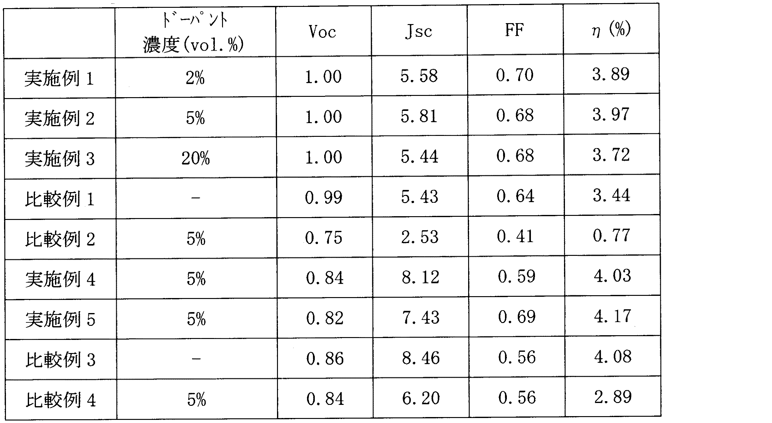
実施例1
25mm×75mm×0.7mm厚のITO透明電極付きガラス基板をイソプロピルアルコール中で超音波洗浄を5分間行なった後、UVオゾン洗浄を30分間実施した。洗浄後の透明電極ライン付きガラス基板を真空蒸着装置の基板ホルダーに装着し、まず下部電極である透明電極ラインが形成されている側の面上に、前記透明電極を覆うようにして、膜厚30nmの化合物Aを抵抗加熱蒸着により、1Å/sで成膜した。続けてその上に膜厚50nmのC60を抵抗加熱蒸着により1Å/sで成膜した。
[Production and evaluation of organic solar cells (sequentially configured elements)]
Example 1
A glass substrate with an ITO transparent electrode having a thickness of 25 mm × 75 mm × 0.7 mm was subjected to ultrasonic cleaning in isopropyl alcohol for 5 minutes, and then UV ozone cleaning was performed for 30 minutes. A glass substrate with a transparent electrode line after cleaning is attached to a substrate holder of a vacuum deposition apparatus, and first, the transparent electrode line as a lower electrode is covered on the surface on which the transparent electrode line is formed, A 30 nm compound A was deposited at 1 Å / s by resistance heating vapor deposition. Subsequently, C 60 having a film thickness of 50 nm was formed thereon at 1 Å / s by resistance heating vapor deposition.
続いて、C60を1Å/sで10nm、化合物Bを0.02Å/sで0.2nmになるように同時蒸着し、nドープ層(混合層)を形成した。続けてその上に、10nmのバソクプロイン(BCP)を抵抗加熱蒸着により1Å/sで成膜した。最後に、連続して対向電極として金属Alを膜厚100nm蒸着させ、有機太陽電池を作製した。素子面積は1.0cm2であった。
素子構成を以下に示す(カッコ内の数値は膜厚(nm)を表す)。
ITO/化合物A(30)/C60(50)/C60:化合物B(10:0.2)/BCP(10)/Al(100)
Subsequently, 10 nm to C 60 with 1 Å / s, compound B was co-deposition to a 0.2nm at 0.02 Å / s, to form n-doped layer (mixed layer). Subsequently, 10 nm bathocuproine (BCP) was formed thereon at 1 Å / s by resistance heating vapor deposition. Finally, metal Al was continuously deposited as a counter electrode with a thickness of 100 nm to produce an organic solar cell. The element area was 1.0 cm 2 .
The element structure is shown below (the numerical value in parenthesis represents the film thickness (nm)).
ITO / Compound A (30) / C 60 (50) / C 60 : Compound B (10: 0.2) / BCP (10) / Al (100)
このように作製した有機太陽電池をAM1.5条件下(光強度(Pin)100mW/cm2)でI−V特性を測定した。開放端電圧(Voc)、短絡電流密度(Jsc)、曲線因子(FF)、光電変換効率(η)を表2に示す。 The thus obtained organic solar battery was measured for IV characteristics under AM1.5 conditions (light intensity (Pin) 100 mW / cm 2 ). Table 2 shows open circuit voltage (Voc), short circuit current density (Jsc), fill factor (FF), and photoelectric conversion efficiency (η).
光電変換効率(η)は次式によって求めた。
実施例2
nドープ層を、C60を1Å/sで10nm、化合物Bを0.05Å/sで0.5nmとなるように同時蒸着して形成した他は、実施例1と同様にして有機太陽電池を作製し、評価した。結果を表2に示す。
Example 2
The n-doped layer, 10 nm of C 60 with 1 Å / s, other formed by co-evaporation so as to 0.5nm at 0.05 Å / s is the compound B, and an organic solar cell in the same manner as in Example 1 Prepared and evaluated. The results are shown in Table 2.
実施例3
nドープ層を、C60を1Å/sで10nm、化合物Bを0.2Å/sで2nmとなるように同時蒸着して形成した他は、実施例1と同様にして有機太陽電池を作製し、評価した。結果を表2に示す。
Example 3
The n-doped layer, 10 nm of C 60 with 1 Å / s, other formed by co-evaporation so that the 2nm at 0.2 Å / s is the compound B, to produce an organic solar cell in the same manner as in Example 1 ,evaluated. The results are shown in Table 2.
比較例1
C60層の膜厚を60nmとし、nドープ層を設けなかった他は実施例1と同様にして有機太陽電池を作製し、評価した。結果を表2に示す。
素子構成を以下に示す(カッコ内の数値は膜厚(nm)を表す)。
ITO/化合物A(30)/C60(60)/BCP(10)/Al(100)
Comparative Example 1
The thickness of the C 60 layers and 60 nm, in addition to not provided n-doped layer to produce an organic solar cell in the same manner as in Example 1 and evaluated. The results are shown in Table 2.
The element structure is shown below (the numerical value in parenthesis represents the film thickness (nm)).
ITO / Compound A (30) / C 60 (60) / BCP (10) / Al (100)
比較例2
C60層を設けず、nドープ層を、C60を1Å/sで60nm、化合物Bを0.05Å/sで3nmとなるように同時蒸着して形成した他は、実施例1と同様にして有機太陽電池を作製し、評価した。結果を表2に示す。
素子構成を以下に示す(カッコ内の数値は膜厚(nm)を表す)。
ITO/化合物A(30)/C60:化合物B(60:3)/BCP(10)/Al(100)
Comparative Example 2
The same as in Example 1, except that the C 60 layer was not provided and the n-doped layer was formed by co-evaporation so that C 60 was 60 nm at 1 60 / s and Compound B was 3 nm at 0.05 Å / s. An organic solar cell was prepared and evaluated. The results are shown in Table 2.
The element structure is shown below (the numerical value in parenthesis represents the film thickness (nm)).
ITO / Compound A (30) / C 60 : Compound B (60: 3) / BCP (10) / Al (100)
実施例4
25mm×75mm×0.7mm厚のITO透明電極付きガラス基板をイソプロピルアルコール中で超音波洗浄を5分間行なった後、UVオゾン洗浄を30分間実施した。洗浄後の透明電極ライン付きガラス基板を真空蒸着装置の基板ホルダーに装着し、まず下部電極である透明電極ラインが形成されている側の面上に、前記透明電極を覆うようにして、膜厚10nmの化合物Cを抵抗加熱蒸着により、1Å/sで成膜した。続けてその上に膜厚10nmのSubNcを抵抗加熱蒸着により1Å/sで成膜した後、続けてその上に膜厚50nmのC60を抵抗加熱蒸着により1Å/sで成膜した。
Example 4
A glass substrate with an ITO transparent electrode having a thickness of 25 mm × 75 mm × 0.7 mm was subjected to ultrasonic cleaning in isopropyl alcohol for 5 minutes, and then UV ozone cleaning was performed for 30 minutes. A glass substrate with a transparent electrode line after cleaning is attached to a substrate holder of a vacuum deposition apparatus, and first, the transparent electrode line as a lower electrode is covered on the surface on which the transparent electrode line is formed, A 10 nm compound C was deposited at 1 蒸 着 / s by resistance heating vapor deposition. After forming at 1 Å / s by resistance heating deposition SubNc of thickness 10nm thereon continues, thereon was formed a C 60 having a thickness of 50nm by resistance heating deposition at 1 Å / s to continue.
続いて、C60を1Å/sで10nm、化合物Bを0.05Å/sで0.5nmになるように同時蒸着し、nドープ層を形成した。その上に、10nmの化合物Dを抵抗加熱蒸着により1Å/sで成膜した。最後に、連続して対向電極として金属Alを膜厚100nm蒸着させ、有機薄膜太陽電池を作製した。素子面積は1.0cm2であった。
このように作製した有機太陽電池について、実施例1と同様に評価した。結果を表2に示す。
素子構成を以下に示す(カッコ内の数値は膜厚(nm)を表す)。
ITO/化合物C(10)/SubNc(10)/C60(50)/C60:化合物B(10:0.5)/化合物D(10)/Al(100)
Subsequently, C 60 was co-evaporated to 1 nm / s to 10 nm and Compound B to 0.05 nm / s to 0.5 nm to form an n-doped layer. On top of this, a compound D of 10 nm was formed at 1 Å / s by resistance heating vapor deposition. Finally, metal Al was continuously deposited as a counter electrode at a film thickness of 100 nm to produce an organic thin film solar cell. The element area was 1.0 cm 2 .
The thus produced organic solar cell was evaluated in the same manner as in Example 1. The results are shown in Table 2.
The element structure is shown below (the numerical value in parenthesis represents the film thickness (nm)).
ITO / Compound C (10) / SubNc (10) / C 60 (50) / C 60 : Compound B (10: 0.5) / Compound D (10) / Al (100)
実施例5
C60層の膜厚を55nmとし、nドープ層をC60を1Å/sで5nm、化合物Bを0.05Å/sで0.25nmとなるように同時蒸着して形成した他は、実施例4と同様にして有機太陽電池を作製し、評価した。結果を表2に示す。
Example 5
The thickness of the C 60 layers and 55 nm, 5 nm and n-doped layer of C 60 with 1 Å / s, except that the compound B was formed by co-evaporation so as to 0.25nm at 0.05 Å / s, the embodiment In the same manner as in Example 4, an organic solar cell was produced and evaluated. The results are shown in Table 2.
比較例3
C60層の膜厚を60nmとし、nドープ層を設けなかった他は実施例4と同様にして有機太陽電池を作製し、評価した。結果を表2に示す。
素子構成を以下に示す(カッコ内の数値は膜厚(nm)を表す)。
ITO/化合物C(10)/SubNc(10)/C60(60)/化合物D(10)/Al(100)
Comparative Example 3
The thickness of the C 60 layers and 60 nm, in addition to not provided n-doped layer to produce an organic solar cell in the same manner as in Example 4, it was evaluated. The results are shown in Table 2.
The element structure is shown below (the numerical value in parenthesis represents the film thickness (nm)).
ITO / Compound C (10) / SubNc (10) / C 60 (60) / Compound D (10) / Al (100)
比較例4
C60層を設けず、nドープ層を、C60を1Å/sで60nm、化合物Bを0.05Å/sで3nmになるように同時蒸着して形成した他は、実施例4と同様にして有機太陽電池を作製し、評価した。結果を表2に示す。
素子構成を以下に示す(カッコ内の数値は膜厚(nm)を表す)。
ITO/化合物C(10)/SubNc(10)/C60:化合物B(60:3)/化合物D(10)/Al(100)
Comparative Example 4
Without providing the C 60 layers, the n-doped layer, 60 nm of C 60 with 1 Å / s, other formed by co-evaporation so that the compound B to 3nm at 0.05 Å / s, in the same manner as in Example 4 An organic solar cell was prepared and evaluated. The results are shown in Table 2.
The element structure is shown below (the numerical value in parenthesis represents the film thickness (nm)).
ITO / Compound C (10) / SubNc (10) / C 60 : Compound B (60: 3) / Compound D (10) / Al (100)
[有機太陽電池の作製・評価(逆構成型素子)]
実施例6
25mm×75mm×0.7mm厚のITO透明電極付きガラス基板をイソプロピルアルコール中で超音波洗浄を5分間行なった後、UVオゾン洗浄を30分間実施した。洗浄後の透明電極ライン付きガラス基板を真空蒸着装置の基板ホルダーに装着し、まず下部電極である透明電極ラインが形成されている側の面上に、前記透明電極を覆うようにして、膜厚0.5nmのCaを抵抗加熱蒸着により、3Å/sで成膜した。
[Fabrication and evaluation of organic solar cells (reverse configuration element)]
Example 6
A glass substrate with an ITO transparent electrode having a thickness of 25 mm × 75 mm × 0.7 mm was subjected to ultrasonic cleaning in isopropyl alcohol for 5 minutes, and then UV ozone cleaning was performed for 30 minutes. A glass substrate with a transparent electrode line after cleaning is attached to a substrate holder of a vacuum deposition apparatus, and first, the transparent electrode line as a lower electrode is covered on the surface on which the transparent electrode line is formed, A film of 0.5 nm Ca was formed at 3 Å / s by resistance heating vapor deposition.
続いて、C60を1Å/sで5nm、化合物Bを0.05Å/sで0.25nmになるように同時蒸着し、nドープ層(混合層)を形成した。その上に膜厚15nmのC70を抵抗加熱蒸着により1Å/sで成膜した。続いて、SubNcを0.1Å/sで5nm、C70を0.4Å/sで20nmになるように同時蒸着し、i層(混合層)を形成した。続いて、膜厚10nmの化合物Cを抵抗加熱蒸着により、1Å/sで成膜した。続いて、化合物Cを1Å/sで30nm、化合物Eを0.05Å/sで1.5nmになるように同時蒸着し、pドープ層(混合層)を形成した。 Subsequently, C 60 was co-evaporated to 1 nm / s to 5 nm and Compound B to 0.05 nm / s to 0.25 nm to form an n-doped layer (mixed layer). It was deposited at 1 Å / s by resistance heating deposition C 70 with a thickness of 15nm thereon. Then, 5 nm to SubNc at 0.1 Å / s, co-deposited C 70 to be 20nm in 0.4 Å / s, to form the i-layer (mixed layer). Subsequently, a compound C having a thickness of 10 nm was formed at 1 Å / s by resistance heating vapor deposition. Subsequently, Compound C was vapor-deposited at 30 nm at 1 Å / s and Compound E at 1.5 nm at 0.05 Å / s to form a p-doped layer (mixed layer).
その上に、5nmのMoO3を抵抗加熱蒸着により1Å/sで成膜した。最後に、連続して対向電極として金属Alを膜厚100nm蒸着させ、有機薄膜太陽電池を作製した。素子面積は1.0cm2であった。
本実施例の素子は、ITOを陰極として用い、対抗電極であるAlを陽極として用いる逆構成型の素子である。このように作製した有機太陽電池について、実施例1と同様に評価した。結果を表2に示す。
素子構成を以下に示す(カッコ内の数値は膜厚(nm)を表す)。
ITO/Ca(0.5)/C60:化合物B(5:0.25)/C70(15)/SubNc:C70(5:20)/化合物C(10)/化合物C:化合物E(30:1.5)/MoO3(5)/Al(100)
On top of that, 5 nm of MoO 3 was deposited at 1 Å / s by resistance heating vapor deposition. Finally, metal Al was continuously deposited as a counter electrode at a film thickness of 100 nm to produce an organic thin film solar cell. The element area was 1.0 cm 2 .
The element of this example is a reverse configuration type element using ITO as a cathode and Al as a counter electrode as an anode. The thus produced organic solar cell was evaluated in the same manner as in Example 1. The results are shown in Table 2.
The element structure is shown below (the numerical value in parenthesis represents the film thickness (nm)).
ITO / Ca (0.5) / C 60 : Compound B (5: 0.25) / C 70 (15) / SubNc: C 70 (5:20) / Compound C (10) / Compound C: Compound E ( 30: 1.5) / MoO 3 (5) / Al (100)
実施例7
nドーパントである化合物Bを化合物Fに変更した他は、実施例6と同様にして有機太陽電池を作製し、評価した。結果を表2に示す。
Example 7
An organic solar cell was prepared and evaluated in the same manner as in Example 6 except that Compound B, which was an n dopant, was changed to Compound F. The results are shown in Table 2.
実施例8
nドーパントである化合物BをCuPcに変更した他は、実施例6と同様にして有機太陽電池を作製し、評価した。結果を表2に示す。
Example 8
An organic solar cell was prepared and evaluated in the same manner as in Example 6 except that the compound B as the n dopant was changed to CuPc. The results are shown in Table 2.
実施例9
nドーパントである化合物Bを化合物Gに変更した他は、実施例6と同様にして有機太陽電池を作製し、評価した。結果を表2に示す。
Example 9
An organic solar cell was produced and evaluated in the same manner as in Example 6 except that Compound B, which was an n dopant, was changed to Compound G. The results are shown in Table 2.
実施例10
nドーパントである化合物BをIr(ppy)3に変更した他は、実施例6と同様にして有機太陽電池を作製し、評価した。結果を表2に示す。
Example 10
An organic solar cell was produced and evaluated in the same manner as in Example 6 except that Compound B as an n dopant was changed to Ir (ppy) 3 . The results are shown in Table 2.
実施例11
nドーパントである化合物BをIr(ppz)3に変更した他は、実施例6と同様にして有機太陽電池を作製し、評価した。結果を表2に示す。
Example 11
An organic solar cell was produced and evaluated in the same manner as in Example 6 except that Compound B as an n dopant was changed to Ir (ppz) 3 . The results are shown in Table 2.
実施例12
nドーパントである化合物BをRu(acac)3に変更した他は、実施例6と同様にして有機太陽電池を作製し、評価した。結果を表2に示す。
Example 12
An organic solar cell was prepared and evaluated in the same manner as in Example 6 except that Compound B as an n dopant was changed to Ru (acac) 3 . The results are shown in Table 2.
実施例13
nドーパントである化合物BをFirpicに変更した他は、実施例6と同様にして有機太陽電池を作製し、評価した。結果を表2に示す。
Example 13
An organic solar cell was prepared and evaluated in the same manner as in Example 6 except that Compound B as the n dopant was changed to Ferpic. The results are shown in Table 2.
実施例14
nドーパントである化合物BをPTCBIに変更した他は、実施例6と同様にして有機太陽電池を作製し、評価した。結果を表2に示す。
Example 14
An organic solar cell was prepared and evaluated in the same manner as in Example 6 except that Compound B as an n dopant was changed to PTCBI. The results are shown in Table 2.
比較例5
nドープ層の成膜において、化合物Bを用いなかった(即ち、非ドープのC60層とした)他は、実施例6と同様にして有機太陽電池を作製し、評価した。結果を表2に示す。
素子構成を以下に示す(カッコ内の数値は膜厚(nm)を表す)。
ITO/Ca/C60(5)/C70(15)/SubNc:C70(5:20)/化合物C(10)/化合物C:化合物E(30:1.5)/MoO3(5)/Al(100)
Comparative Example 5
In the deposition of the n-doped layer, not using the compound B (i.e., to a C 60 layer of undoped) others, to produce an organic solar cell in the same manner as in Example 6, was evaluated. The results are shown in Table 2.
The element structure is shown below (the numerical value in parenthesis represents the film thickness (nm)).
ITO / Ca / C 60 (5) / C 70 (15) / SubNc: C 70 (5:20) / Compound C (10) / Compound C: Compound E (30: 1.5) / MoO 3 (5) / Al (100)
実施例15
実施例6と同様にしてITO透明電極付きガラス基板にCaを成膜後、化合物Dを1Å/sで5nmになるように抵抗加熱蒸着により成膜した。続いて、実施例6と同様にしてnドープ層以降を形成して有機太陽電池を作製し、評価した。結果を表2に示す。
素子構成を以下に示す(カッコ内の数値は膜厚(nm)を表す)。
ITO/Ca/化合物D(5)/C60:化合物B(5:0.25)/C70(15)/SubNc:C70(5:20)/化合物C(10)/化合物C:化合物E(30:1.5)/MoO3(5)/Al(100)
Example 15
In the same manner as in Example 6, after depositing Ca on a glass substrate with an ITO transparent electrode, Compound D was deposited by resistance heating vapor deposition so as to be 5 nm at 1 Å / s. Subsequently, the n-doped layer and subsequent layers were formed in the same manner as in Example 6 to produce and evaluate an organic solar cell. The results are shown in Table 2.
The element structure is shown below (the numerical value in parenthesis represents the film thickness (nm)).
ITO / Ca / Compound D (5) / C 60 : Compound B (5: 0.25) / C 70 (15) / SubNc: C 70 (5:20) / Compound C (10) / Compound C: Compound E (30: 1.5) / MoO 3 (5) / Al (100)
実施例16
実施例6と同様にしてITO透明電極付きガラス基板にCaを成膜後、化合物Dを1Å/sで5nmになるように抵抗加熱蒸着により成膜した。続いて、実施例6と同様にしてnドープ層を成膜し、その上にC60を1Å/sで5nmになるように抵抗加熱蒸着により成膜した。その後、実施例6と同様にしてC70層以降を形成して有機太陽電池を作製し、評価した。結果を表2に示す。
素子構成を以下に示す(カッコ内の数値は膜厚(nm)を表す)。
ITO/Ca/化合物D(5)/C60:化合物B(5:0.25)/C60(5)/C70(15)/SubNc:C70(5:20)/化合物C(10)/化合物C:化合物E(30:1.5)/MoO3(5)/Al(100)
Example 16
In the same manner as in Example 6, after depositing Ca on a glass substrate with an ITO transparent electrode, Compound D was deposited by resistance heating vapor deposition so as to be 5 nm at 1 Å / s. Subsequently, an n-doped layer was formed in the same manner as in Example 6, and C 60 was formed thereon by resistance heating vapor deposition so as to be 5 nm at 1 Å / s. Thereafter, the C70 layer and subsequent layers were formed in the same manner as in Example 6 to produce and evaluate an organic solar cell. The results are shown in Table 2.
The element structure is shown below (the numerical value in parenthesis represents the film thickness (nm)).
ITO / Ca / Compound D (5) / C 60 : Compound B (5: 0.25) / C 60 (5) / C 70 (15) / SubNc: C 70 (5:20) / Compound C (10) / Compound C: Compound E (30: 1.5) / MoO 3 (5) / Al (100)
比較例6
実施例6と同様にしてITO透明電極付きガラス基板にCaを成膜後、化合物Dを1Å/sで5nmになるように抵抗加熱蒸着により成膜した。続いて、nドープ層を成膜せずに、C60を1Å/sで5nmになるように抵抗加熱蒸着により成膜した。その後、実施例6と同様にしてC70層以降を形成して有機太陽電池を作製し、評価した。結果を表2に示す。
素子構成を以下に示す(カッコ内の数値は膜厚(nm)を表す)。
ITO/Ca/化合物D(5)/C60(5)/C70(15)/SubNc:C70(5:20)/化合物C(10)/化合物C:化合物E(30:1.5)/MoO3(5)/Al(100)
Comparative Example 6
In the same manner as in Example 6, after depositing Ca on a glass substrate with an ITO transparent electrode, Compound D was deposited by resistance heating vapor deposition so as to be 5 nm at 1 Å / s. Subsequently, without forming an n-doped layer, C 60 was deposited by resistance heating vapor deposition so as to be 5 nm at 1 Å / s. Thereafter, the C70 layer and subsequent layers were formed in the same manner as in Example 6 to produce and evaluate an organic solar cell. The results are shown in Table 2.
The element structure is shown below (the numerical value in parenthesis represents the film thickness (nm)).
ITO / Ca / Compound D (5) / C 60 (5) / C 70 (15) / SubNc: C 70 (5:20) / Compound C (10) / Compound C: Compound E (30: 1.5) / MoO 3 (5) / Al (100)
[有機太陽電池の作製・評価(タンデム型素子)]
実施例17
実施例6と同様にしてpドープ層(混合層)まで形成した。
続けて、2nmのMoO3を抵抗加熱蒸着により1Å/sで成膜し、金属Alを膜厚1nm蒸着させ、膜厚0.5nmのCaを抵抗加熱蒸着により、3Å/sで成膜して中間電極を形成した。
[Production and evaluation of organic solar cells (tandem type elements)]
Example 17
In the same manner as in Example 6, a p-doped layer (mixed layer) was formed.
Subsequently, 2 nm of MoO 3 was deposited at 1 蒸 着 / s by resistance heating vapor deposition, metal Al was deposited at a thickness of 1 nm, and Ca with a thickness of 0.5 nm was deposited at 3 Å / s by resistance heating deposition. An intermediate electrode was formed.
その後、C60を1Å/sで5nm、化合物Bを0.05Å/sで0.25nmになるように同時蒸着し、nドープ層(混合層)を形成した。その上に膜厚15nmのC70を抵抗加熱蒸着により1Å/sで成膜した。続いて、SubNcを0.1Å/sで5nm、C70を0.4Å/sで20nmになるように同時蒸着し、i層(混合層)を形成した。続いて、膜厚10nmの化合物Cを抵抗加熱蒸着により、1Å/sで成膜した。続いて、化合物Cを1Å/sで30nm、化合物Eを0.05Å/sで1.5nmになるように同時蒸着し、pドープ層(混合層)を形成した。 Thereafter, C 60 was co-evaporated to 1 nm / s to 5 nm and Compound B to 0.05 nm / s to 0.25 nm to form an n-doped layer (mixed layer). It was deposited at 1 Å / s by resistance heating deposition C 70 with a thickness of 15nm thereon. Then, 5 nm to SubNc at 0.1 Å / s, co-deposited C 70 to be 20nm in 0.4 Å / s, to form the i-layer (mixed layer). Subsequently, a compound C having a thickness of 10 nm was formed at 1 Å / s by resistance heating vapor deposition. Subsequently, Compound C was vapor-deposited at 30 nm at 1 Å / s and Compound E at 1.5 nm at 0.05 Å / s to form a p-doped layer (mixed layer).
その上に、5nmのMoO3を抵抗加熱蒸着により1Å/sで成膜した。最後に、連続して対向電極として金属Alを膜厚100nm蒸着させ、有機薄膜太陽電池を作製した。素子面積は1.0cm2であった。
本実施例の素子はタンデム型の素子である。このように作製した有機太陽電池について、実施例6と同様に評価した。結果を表2に示す。
素子構成を以下に示す(カッコ内の数値は膜厚(nm)を表す)。
ITO/Ca(0.5)/C60:化合物B(5:0.25)/C70(15)/SubNc:C70(5:20)/化合物C(10)/化合物C:化合物E(30:1.5)/MoO3(2)/Al(1)/Ca(0.5)/C60:化合物B(5:0.25)/C70(15)/SubNc:C70(5:20)/化合物C(10)/化合物C:化合物E(30:1.5)/MoO3(5)/Al(100)
On top of that, 5 nm of MoO 3 was deposited at 1 Å / s by resistance heating vapor deposition. Finally, metal Al was continuously deposited as a counter electrode at a film thickness of 100 nm to produce an organic thin film solar cell. The element area was 1.0 cm 2 .
The element of this example is a tandem element. The thus produced organic solar cell was evaluated in the same manner as in Example 6. The results are shown in Table 2.
The element structure is shown below (the numerical value in parenthesis represents the film thickness (nm)).
ITO / Ca (0.5) / C 60 : Compound B (5: 0.25) / C 70 (15) / SubNc: C 70 (5:20) / Compound C (10) / Compound C: Compound E ( 30: 1.5) / MoO 3 (2) / Al (1) / Ca (0.5) / C 60 : Compound B (5: 0.25) / C 70 (15) / SubNc: C 70 (5 : 20) / Compound C (10) / Compound C: Compound E (30: 1.5) / MoO 3 (5) / Al (100)
実施例18
中間電極に金属Alを用いなかった他は、実施例17と同様にして有機太陽電池を作製し、評価した。結果を表2に示す。
Example 18
An organic solar cell was prepared and evaluated in the same manner as in Example 17 except that metal Al was not used for the intermediate electrode. The results are shown in Table 2.
比較例7
2つのnドープ層の成膜において、化合物Bを用いなかった(即ち、非ドープのC60層とした)他は、実施例17と同様にして有機太陽電池を作製し、評価した。結果を表2に示す。
素子構成を以下に示す(カッコ内の数値は膜厚(nm)を表す)。
ITO/Ca(0.5)/C60(5)/C70(15)/SubNc:C70(5:20)/化合物C(10)/化合物C:化合物E(30:1.5)/MoO3(2)/Al(1)/Ca(0.5)/C60(5)/C70(15)/SubNc:C70(5:20)/化合物C(10)/化合物C:化合物E(30:1.5)/MoO3(5)/Al(100)
Comparative Example 7
In the two forming the n-doped layer, not using the compound B (i.e., to a C 60 layer of undoped) others, to produce an organic solar cell in the same manner as in Example 17, was evaluated. The results are shown in Table 2.
The element structure is shown below (the numerical value in parenthesis represents the film thickness (nm)).
ITO / Ca (0.5) / C 60 (5) / C 70 (15) / SubNc: C70 (5:20) / Compound C (10) / Compound C: Compound E (30: 1.5) / MoO 3 (2) / Al (1) / Ca (0.5) / C 60 (5) / C 70 (15) / SubNc: C 70 (5:20) / Compound C (10) / Compound C: Compound E (30: 1.5) / MoO 3 (5) / Al (100)
比較例8
中間電極に金属Alを用いなかった他は、比較例7と同様にして有機太陽電池を作製し、評価した。結果を表2に示す。
Comparative Example 8
An organic solar cell was prepared and evaluated in the same manner as in Comparative Example 7 except that metal Al was not used for the intermediate electrode. The results are shown in Table 2.
素子作製に用いた化合物の構造を以下に示す。
本発明の有機太陽電池は時計、携帯電話及びモバイルパソコン等の各種装置、電化製品等の電源又は補助電源として使用できる。充電機能のある二次電池と組み合わせ、暗所においても使用可能とし、適用用途を拡げることも可能である。 The organic solar cell of the present invention can be used as a power source or auxiliary power source for various devices such as watches, mobile phones and mobile personal computers, and electrical appliances. Combined with a rechargeable battery with a charging function, it can be used in the dark, and the application can be expanded.
Claims (8)
Priority Applications (1)
| Application Number | Priority Date | Filing Date | Title |
|---|---|---|---|
| JP2012222105A JP2014075476A (en) | 2012-10-04 | 2012-10-04 | Organic solar cell |
Applications Claiming Priority (1)
| Application Number | Priority Date | Filing Date | Title |
|---|---|---|---|
| JP2012222105A JP2014075476A (en) | 2012-10-04 | 2012-10-04 | Organic solar cell |
Publications (1)
| Publication Number | Publication Date |
|---|---|
| JP2014075476A true JP2014075476A (en) | 2014-04-24 |
Family
ID=50749429
Family Applications (1)
| Application Number | Title | Priority Date | Filing Date |
|---|---|---|---|
| JP2012222105A Pending JP2014075476A (en) | 2012-10-04 | 2012-10-04 | Organic solar cell |
Country Status (1)
| Country | Link |
|---|---|
| JP (1) | JP2014075476A (en) |
Cited By (2)
| Publication number | Priority date | Publication date | Assignee | Title |
|---|---|---|---|---|
| JP2016015487A (en) * | 2014-07-01 | 2016-01-28 | ピョクサン ペイント アンド コーティングス カンパニー,リミテッド | Compound for phosphorescence host, and organic light-emitting device including the same |
| JP2016529705A (en) * | 2013-07-24 | 2016-09-23 | アイメック・ヴェーゼットウェーImec Vzw | Organic solar cells with improved photocurrent |
-
2012
- 2012-10-04 JP JP2012222105A patent/JP2014075476A/en active Pending
Cited By (2)
| Publication number | Priority date | Publication date | Assignee | Title |
|---|---|---|---|---|
| JP2016529705A (en) * | 2013-07-24 | 2016-09-23 | アイメック・ヴェーゼットウェーImec Vzw | Organic solar cells with improved photocurrent |
| JP2016015487A (en) * | 2014-07-01 | 2016-01-28 | ピョクサン ペイント アンド コーティングス カンパニー,リミテッド | Compound for phosphorescence host, and organic light-emitting device including the same |
Similar Documents
| Publication | Publication Date | Title |
|---|---|---|
| JP5625002B2 (en) | Multilayer organic photosensitive device | |
| JP5580976B2 (en) | Organic thin film solar cell | |
| TWI661588B (en) | Hybrid planar-graded heterojunction for organic photovoltaics | |
| JP5583809B2 (en) | Organic solar cell | |
| KR20200018718A (en) | Organic photovoltaic cell incorporating electron conducting exciton blocking layers | |
| KR20110060956A (en) | Organic tandem solar cell | |
| US20140014183A1 (en) | Organic thin-film solar cell and organic thin-film solar cell module | |
| WO2013102985A1 (en) | Organic photoelectric conversion element and organic thin-film solar battery module | |
| WO2013035305A1 (en) | Organic solar cell | |
| JP2014038975A (en) | Organic thin-film solar cell module | |
| JP5260379B2 (en) | Organic thin film solar cell | |
| JP2014075476A (en) | Organic solar cell | |
| JP2014090093A (en) | Tandem type organic thin-film solar cell | |
| JP5469943B2 (en) | Photoelectric conversion element | |
| JP2011233692A (en) | Photoelectric converter, organic solar cell and photoelectric conversion apparatus using these | |
| JP2011023594A (en) | Photoelectric converting element | |
| JP5499193B2 (en) | Organic thin film solar cell | |
| JP2014077042A (en) | Organic thin film solar cell material including dibenzopyrromethene compound | |
| JP5560132B2 (en) | Organic thin film solar cell material and organic thin film solar cell using the same | |
| JP2014194998A (en) | Organic solar cell | |
| JP2014195030A (en) | Organic thin film solar cell containing InClPc |