[go: up one dir, main page]

JP2014072200A - Photoelectric conversion device and method of manufacturing the same - Google Patents

Photoelectric conversion device and method of manufacturing the same Download PDF

Info

Publication number
JP2014072200A
JP2014072200A JP2012214347A JP2012214347A JP2014072200A JP 2014072200 A JP2014072200 A JP 2014072200A JP 2012214347 A JP2012214347 A JP 2012214347A JP 2012214347 A JP2012214347 A JP 2012214347A JP 2014072200 A JP2014072200 A JP 2014072200A
Authority
JP
Japan
Prior art keywords
layer
photoelectric conversion
interface control
conversion device
semiconductor layer
Prior art date
Legal status (The legal status is an assumption and is not a legal conclusion. Google has not performed a legal analysis and makes no representation as to the accuracy of the status listed.)
Pending
Application number
JP2012214347A
Other languages
Japanese (ja)
Inventor
Hiroshi Matsubara
弘 松原
Current Assignee (The listed assignees may be inaccurate. Google has not performed a legal analysis and makes no representation or warranty as to the accuracy of the list.)
Sharp Corp
Original Assignee
Sharp Corp
Priority date (The priority date is an assumption and is not a legal conclusion. Google has not performed a legal analysis and makes no representation as to the accuracy of the date listed.)
Filing date
Publication date
Application filed by Sharp Corp filed Critical Sharp Corp
Priority to JP2012214347A priority Critical patent/JP2014072200A/en
Publication of JP2014072200A publication Critical patent/JP2014072200A/en
Pending legal-status Critical Current

Links

Images

Classifications

    • YGENERAL TAGGING OF NEW TECHNOLOGICAL DEVELOPMENTS; GENERAL TAGGING OF CROSS-SECTIONAL TECHNOLOGIES SPANNING OVER SEVERAL SECTIONS OF THE IPC; TECHNICAL SUBJECTS COVERED BY FORMER USPC CROSS-REFERENCE ART COLLECTIONS [XRACs] AND DIGESTS
    • Y02TECHNOLOGIES OR APPLICATIONS FOR MITIGATION OR ADAPTATION AGAINST CLIMATE CHANGE
    • Y02EREDUCTION OF GREENHOUSE GAS [GHG] EMISSIONS, RELATED TO ENERGY GENERATION, TRANSMISSION OR DISTRIBUTION
    • Y02E10/00Energy generation through renewable energy sources
    • Y02E10/50Photovoltaic [PV] energy

Landscapes

  • Photovoltaic Devices (AREA)

Abstract

PROBLEM TO BE SOLVED: To provide a photoelectric conversion device with an i-type amorphous silicon carbide semiconductor layer that has excellent photoelectric conversion characteristics.SOLUTION: A photoelectric conversion device includes a stack of a first conductive layer, a first photoelectric conversion layer, and a second conductive layer in that order. The first photoelectric conversion layer has a p-type silicon-based semiconductor layer, an i-type amorphous silicon carbide semiconductor layer, an interface control layer, and an n-type silicon-based semiconductor layer that are sequentially stacked from the first conductive layer side to the second conductive layer side. The interface control layer contains silicon atoms, carbon atoms, and oxygen atoms.

Description

本発明は、光電変換装置に関し、さらに詳しくは光電変換装置の高効率化技術に関する。また、本発明は光電変換装置の製造方法に関する。   The present invention relates to a photoelectric conversion device, and more particularly to a technology for improving the efficiency of a photoelectric conversion device. The present invention also relates to a method for manufacturing a photoelectric conversion device.

近年、電力エネルギー源および地球温暖化の問題から、再生可能エネルギーの代表格である太陽電池に注目が集まっている。太陽電池の中で現在最も普及しているのは、単結晶シリコン、多結晶シリコン等のバルク結晶を利用したものであるが、バルク結晶系太陽電池は数百μmの厚さのシリコン基板を用いているため、大幅なコスト低下が難しい。これに対して、薄膜シリコン系太陽電池は、大面積化が容易であり、膜厚がバルク結晶系太陽電池の1/100程度と薄いため材料費が安く低コスト化が見込めるなどのメリットがある。しかしながら、薄膜シリコン系太陽電池は、結晶系太陽電池と比較して発電効率が低く、光電変換特性の向上が重要な課題となっている。   2. Description of the Related Art In recent years, attention has been focused on solar cells, which are representative of renewable energy, due to power energy sources and global warming issues. The most widespread among solar cells are those using bulk crystals such as single crystal silicon and polycrystalline silicon, but bulk crystal solar cells use a silicon substrate with a thickness of several hundred μm. Therefore, it is difficult to reduce the cost significantly. In contrast, thin-film silicon solar cells are easy to increase in area and have a merit that the material cost is low and the cost can be reduced because the film thickness is as thin as about 1/100 that of bulk crystal solar cells. . However, thin-film silicon solar cells have lower power generation efficiency than crystalline solar cells, and improvement of photoelectric conversion characteristics is an important issue.

上記薄膜シリコン系太陽電池の光電変換層は、光吸収層に水素化非晶質シリコン系半導体を用いた非晶質シリコン太陽電池と、光吸収層に水素化微結晶シリコン系半導体を用いた、微結晶シリコン太陽電池とに大別される。また、両者のバンドギャップ、分光感度特性の違いを利用し、この両者を積層した積層型薄膜シリコン系太陽電池も、近年特に注目を浴びている。積層型薄膜シリコン系太陽電池の高効率化においては、もちろん非晶質シリコン層、微結晶シリコン層両方の高効率化が必要である。   The photoelectric conversion layer of the thin-film silicon-based solar cell uses an amorphous silicon solar cell using a hydrogenated amorphous silicon-based semiconductor for the light absorption layer, and a hydrogenated microcrystalline silicon-based semiconductor for the light absorption layer. Broadly divided into microcrystalline silicon solar cells. Also, in recent years, a stacked thin film silicon solar cell in which both of these are used to take advantage of the difference in band gap and spectral sensitivity characteristics has attracted particular attention in recent years. In order to increase the efficiency of a stacked thin film silicon solar cell, it is of course necessary to increase the efficiency of both the amorphous silicon layer and the microcrystalline silicon layer.

また、非晶質シリコン太陽電池の開放電圧を高めるために、i層を非晶質シリコンカーバイド層とした薄膜太陽電池の開発も行なわれている。特開平8−116080号公報(特許文献1)においては、i層を非晶質シリコンカーバイド層とし、さらにp層を微結晶シリコン層とし、その微結晶シリコンの体積率や非晶質相の結合水素量を調整して、開放電圧を向上することが記載されている。   In addition, in order to increase the open circuit voltage of amorphous silicon solar cells, thin film solar cells in which the i layer is an amorphous silicon carbide layer have been developed. In Japanese Patent Application Laid-Open No. 8-111080 (Patent Document 1), the i layer is an amorphous silicon carbide layer, and the p layer is a microcrystalline silicon layer. It is described that the open-circuit voltage is improved by adjusting the amount of hydrogen.

特開平8−116080号公報Japanese Patent Application Laid-Open No. 8-111080

しかしながら、特許文献1に記載されている非晶質シリコンカーバイド層からなるi層を有する光電変換素子によってもその開放電圧の向上は十分ではなく、さらなる特性の向上が望まれていた。   However, even with the photoelectric conversion element having an i layer composed of an amorphous silicon carbide layer described in Patent Document 1, the open-circuit voltage is not sufficiently improved, and further improvement in characteristics has been desired.

本発明は、i型非晶質シリコンカーバイド半導体層を有する光電変換装置において、優れた光電変換特性を有する光電変換装置およびその製造方法を提供することを目的とする。   An object of the present invention is to provide a photoelectric conversion device having excellent photoelectric conversion characteristics in a photoelectric conversion device having an i-type amorphous silicon carbide semiconductor layer, and a method for manufacturing the photoelectric conversion device.

本発明者は、i型非晶質シリコンカーバイド半導体層を備えpin接合を有する光電変換装置において、i型非晶質シリコンカーバイド半導体層とn型半導体層の間に特定の層を設けることにより、短絡電流密度および開放電圧を向上させることができることを見出し、本発明を完成するに至った。本発明は、以下のものを含む。   The inventor has provided a specific layer between an i-type amorphous silicon carbide semiconductor layer and an n-type semiconductor layer in a photoelectric conversion device having an i-type amorphous silicon carbide semiconductor layer and having a pin junction, The inventors have found that the short circuit current density and the open circuit voltage can be improved, and have completed the present invention. The present invention includes the following.

[1]第1導電層、第1光電変換層と、第2導電層がこの順で積層されてなる光電変換装置であって、
第1光電変換層は、第1導電層側から第2導電層側に向けて順に積層された、p型シリコン系半導体層と、i型非晶質シリコンカーバイド半導体層と、界面制御層と、n型シリコン系半導体層と、を有し、
界面制御層は、シリコン原子、炭素原子および酸素原子を含む、光電変換装置。
[1] A photoelectric conversion device in which a first conductive layer, a first photoelectric conversion layer, and a second conductive layer are laminated in this order,
The first photoelectric conversion layer is sequentially stacked from the first conductive layer side to the second conductive layer side, a p-type silicon-based semiconductor layer, an i-type amorphous silicon carbide semiconductor layer, an interface control layer, an n-type silicon-based semiconductor layer,
The interface control layer is a photoelectric conversion device including silicon atoms, carbon atoms, and oxygen atoms.

[2]上記界面制御層の酸素濃度は、1×10²⁰(atoms/cm)以上1×1022(atoms/cm)以下である、[1]に記載の光電変換装置。 [2] The photoelectric conversion device according to [1], wherein the interface control layer has an oxygen concentration of 1 × 10 20 (atoms / cm 3 ) or more and 1 × 10 22 (atoms / cm 3 ) or less.

[3]上記界面制御層において、層厚方向の酸素濃度の極大値を有する、[1]または[2]に記載の光電変換装置。   [3] The photoelectric conversion device according to [1] or [2], wherein the interface control layer has a maximum value of oxygen concentration in a layer thickness direction.

[4]上記界面制御層の炭素濃度は、1×10²⁰(atoms/cm)以上2×1021(atoms/cm)以下である、[1]〜[3]のいずれかに記載の光電変換装置。 [4] The carbon concentration in the interface control layer is 1 × 10 20 (atoms / cm 3 ) or more and 2 × 10 21 (atoms / cm 3 ) or less, according to any one of [1] to [3] Photoelectric conversion device.

[5]上記界面制御層の厚さは100nm以下である、[1]〜[4]のいずれかに記載の光電変換装置。   [5] The photoelectric conversion device according to any one of [1] to [4], wherein the interface control layer has a thickness of 100 nm or less.

[6]上記i型非晶質シリコンカーバイド半導体層の炭素濃度は1×10²²(atoms/cm)以下である、[1]〜[5]のいずれかに記載の光電変換装置。 [6] The photoelectric conversion device according to any one of [1] to [5], wherein the carbon concentration of the i-type amorphous silicon carbide semiconductor layer is 1 × 10 22 (atoms / cm 3 ) or less.

[7]上記界面制御層の酸素濃度は上記i型非晶質シリコンカーバイド半導体層の酸素濃度よりも高く、上記界面制御層の炭素濃度は上記i型非晶質シリコンカーバイド半導体層の炭素濃度よりも低い、[1]〜[6]のいずれかに記載の光電変換装置。   [7] The oxygen concentration of the interface control layer is higher than the oxygen concentration of the i-type amorphous silicon carbide semiconductor layer, and the carbon concentration of the interface control layer is higher than the carbon concentration of the i-type amorphous silicon carbide semiconductor layer. The photoelectric conversion device according to any one of [1] to [6].

[8]上記界面制御層は、ラマン散乱測定による結晶シリコンのピークが観測されない、[1]〜[7]のいずれかに記載の光電変換装置。   [8] The photoelectric conversion device according to any one of [1] to [7], wherein the interface control layer has no crystalline silicon peak observed by Raman scattering measurement.

[9]上記第1光電変換層において、上記界面制御層のバンドギャップEsと、上記i型非晶質シリコンカーバイド半導体層のバンドギャップEiとが、以下の式:
Ei−0.05[eV]≦Es≦Ei+0.20[eV]
で表わされる関係を満たす、[1]〜[8]のいずれかに記載の光電変換装置。
[9] In the first photoelectric conversion layer, the band gap Es of the interface control layer and the band gap Ei of the i-type amorphous silicon carbide semiconductor layer are expressed by the following formula:
Ei−0.05 [eV] ≦ Es ≦ Ei + 0.20 [eV]
The photoelectric conversion device according to any one of [1] to [8], which satisfies a relationship represented by:

[10]上記第1導電層と上記第2導電層との間に、更に第2光電変換層を有する[1]〜[9]のいずれかに記載の光電変換装置。   [10] The photoelectric conversion device according to any one of [1] to [9], further including a second photoelectric conversion layer between the first conductive layer and the second conductive layer.

[11]透光性絶縁基板を備え、当該透光性絶縁基板上に、上記第1導電層、上記第1光電変換層、上記第2導電層がこの順で積層されてなる[1]〜[10]のいずれかに記載の光電変換装置。   [11] A translucent insulating substrate is provided, and the first conductive layer, the first photoelectric conversion layer, and the second conductive layer are stacked in this order on the translucent insulating substrate. [10] The photoelectric conversion device according to any one of [10].

[12]非透光性絶縁基板を備え、当該非透光性絶縁基板上に、上記第2導電層、上記第1光電変換層、上記第1導電層がこの順で積層されてなる[1]〜[10]のいずれかに記載の光電変換装置。   [12] A non-translucent insulating substrate is provided, and the second conductive layer, the first photoelectric conversion layer, and the first conductive layer are laminated in this order on the non-translucent insulating substrate [1] ] The photoelectric conversion apparatus in any one of [10].

[13][1]に記載の光電変換装置の製造方法であって、
シリコン原子、炭素原子および酸素原子を含むガスを供給して前記界面制御層を形成する工程を有する、光電変換装置の製造方法。
[13] A method for manufacturing the photoelectric conversion device according to [1],
A method for manufacturing a photoelectric conversion device, comprising a step of supplying a gas containing silicon atoms, carbon atoms, and oxygen atoms to form the interface control layer.

[14]上記ガスは、二酸化炭素を含む、[13]に記載の光電変換装置の製造方法。   [14] The method for manufacturing a photoelectric conversion device according to [13], wherein the gas includes carbon dioxide.

本発明によると、開放電圧の向上した光電変換装置を提供することができる。   According to the present invention, a photoelectric conversion device with an improved open circuit voltage can be provided.

第1の実施形態の光電変換装置の構成を概略的に示す断面図である。It is sectional drawing which shows schematically the structure of the photoelectric conversion apparatus of 1st Embodiment. 第1および第2の実施形態で用いられるプラズマCVD装置の構成の一部を模式的に示す断面図である。It is sectional drawing which shows typically a part of structure of the plasma CVD apparatus used by 1st and 2nd embodiment. 第2の実施形態の光電変換装置の構成を概略的に示す断面図である。It is sectional drawing which shows schematically the structure of the photoelectric conversion apparatus of 2nd Embodiment. 実施例1の光電変換装置における層厚方向の距離と原子濃度の関係を示す図である。It is a figure which shows the relationship of the distance of the layer thickness direction in the photoelectric conversion apparatus of Example 1, and atomic concentration. 実施例2の光電変換装置における層厚方向の距離と原子濃度の関係を示す図である。It is a figure which shows the relationship of the distance of the layer thickness direction and atomic concentration in the photoelectric conversion apparatus of Example 2. FIG.

本発明の光電変換装置は、第1導電層、第1光電変換層、第2導電層がこの順で積層されてなる。第1光電変換層は、第1導電層側から第2導電層側に向けて順に積層されている、p型シリコン系半導体層と、i型非晶質シリコンカーバイド半導体層と、シリコン原子、炭素原子および酸素原子を含む界面制御層と、n型シリコン系半導体層と、を有する。以下、図面を参照しながら、本発明の光電変換装置について詳細に説明する。   The photoelectric conversion device of the present invention is formed by laminating a first conductive layer, a first photoelectric conversion layer, and a second conductive layer in this order. The first photoelectric conversion layer is sequentially stacked from the first conductive layer side to the second conductive layer side, the p-type silicon-based semiconductor layer, the i-type amorphous silicon carbide semiconductor layer, the silicon atom, the carbon It has an interface control layer containing atoms and oxygen atoms, and an n-type silicon-based semiconductor layer. Hereinafter, the photoelectric conversion device of the present invention will be described in detail with reference to the drawings.

[第1の実施形態]
(光電変換装置の構成)
図1は、第1の実施形態の光電変換装置の構成を概略的に示す断面図である。図1に示すように、第1の実施形態における光電変換装置100は、基板11上に、第1導電層12と、第1光電変換層10と、第2導電層17がこの順で積層されてなる。光電変換装置100は、基板11側から光を入射させるスーパーストレート型である。光電変換装置100において、基板11側を光入射側、第2導電層17側を裏面側ということにする。
[First Embodiment]
(Configuration of photoelectric conversion device)
FIG. 1 is a cross-sectional view schematically showing the configuration of the photoelectric conversion apparatus according to the first embodiment. As shown in FIG. 1, in the photoelectric conversion device 100 according to the first embodiment, a first conductive layer 12, a first photoelectric conversion layer 10, and a second conductive layer 17 are stacked in this order on a substrate 11. It becomes. The photoelectric conversion device 100 is a super straight type in which light is incident from the substrate 11 side. In the photoelectric conversion device 100, the substrate 11 side is referred to as a light incident side, and the second conductive layer 17 side is referred to as a back side.

基板11は、透光性を有する材料により構成される透光性絶縁基板である。基板11は、たとえばガラスやポリイミド等の樹脂などにより構成され、プラズマCVD法による半導体層製膜工程において、耐熱性および透光性を有するものであることが好ましい。   The substrate 11 is a translucent insulating substrate made of a translucent material. The substrate 11 is preferably made of, for example, a resin such as glass or polyimide, and has heat resistance and translucency in the semiconductor layer formation step by the plasma CVD method.

第1導電層12は、透光性を有する材料により構成される。第1導電層12は、たとえばSnO、酸化インジウム錫(ITO)などにより構成することができる。基板11および第1導電層12の厚さおよび形状は特に限定されない。 The first conductive layer 12 is made of a light transmissive material. The first conductive layer 12 can be made of, for example, SnO 2 , indium tin oxide (ITO), or the like. The thickness and shape of the substrate 11 and the first conductive layer 12 are not particularly limited.

第2導電層17は、第1光電変換層10に近い側から順に積層された、透明導電膜17aと金属膜17bとからなる。透明導電膜17aは、たとえばSnO、ITO、ZnOなどにより構成することができる。金属膜17bは、たとえば銀、アルミニウム、チタン、パラジウムなどにより構成することができる。第2導電層17は、金属膜17bのみからなる構成であってもよい。 The 2nd conductive layer 17 consists of the transparent conductive film 17a and the metal film 17b which were laminated | stacked in order from the side close | similar to the 1st photoelectric converting layer 10. FIG. The transparent conductive film 17a can be made of, for example, SnO 2 , ITO, ZnO or the like. The metal film 17b can be made of, for example, silver, aluminum, titanium, palladium, or the like. The second conductive layer 17 may be configured only by the metal film 17b.

第1光電変換層10は、p型シリコン系半導体層13と、i型非晶質シリコンカーバイド半導体層14と、シリコン原子、炭素原子および酸素原子を含む界面制御層15と、n型シリコン系半導体層16が順に積層され、基板11側からp−i−nの接合構造を有する。   The first photoelectric conversion layer 10 includes a p-type silicon-based semiconductor layer 13, an i-type amorphous silicon carbide semiconductor layer 14, an interface control layer 15 including silicon atoms, carbon atoms, and oxygen atoms, and an n-type silicon-based semiconductor. The layers 16 are sequentially stacked and have a p-i-n junction structure from the substrate 11 side.

光電変換装置100においては、酸素および炭素を含む界面制御層15を有することにより、高い開放電圧が得られる。これは、酸素および炭素を含む界面制御層15が、i型非晶質シリコンカーバイド半導体層よりも価電子帯の上端のエネルギー準位Evおよび伝導帯の下端のエネルギー準位Ecが深い準位を取るため、正孔のn層側への拡散が低減され逆方向飽和電流が改善して、開放電圧が向上することによると考えられる。   In the photoelectric conversion device 100, by having the interface control layer 15 containing oxygen and carbon, a high open circuit voltage can be obtained. This is because the interface control layer 15 containing oxygen and carbon has a deeper energy level Ev at the upper end of the valence band and an energy level Ec at the lower end of the conduction band than the i-type amorphous silicon carbide semiconductor layer. Therefore, it is considered that the diffusion of holes to the n layer side is reduced, the reverse saturation current is improved, and the open-circuit voltage is improved.

また、界面制御層15のバンドギャップEsと、i型非晶質シリコンカーバイド半導体層14のバンドギャップEiとは以下の関係を満たすことが好ましい。   The band gap Es of the interface control layer 15 and the band gap Ei of the i-type amorphous silicon carbide semiconductor layer 14 preferably satisfy the following relationship.

Ei−0.05[eV]≦Es≦Ei+0.20[eV]
Es<Ei−0.05[eV]の場合、界面制御層15において、i型シリコン系半導体層14よりも価電子帯の上端のエネルギー準位Evが深い準位を取ることが難しい場合があり、Es>Ei+0.20[eV]の場合、酸素や炭素の添加物が多すぎて界面制御層15の膜質を悪化させてしまうため、本発明の効果である短絡電流密度および開放電圧を向上させることが難しい場合がある。
Ei−0.05 [eV] ≦ Es ≦ Ei + 0.20 [eV]
In the case of Es <Ei−0.05 [eV], it may be difficult for the interface control layer 15 to take the deep energy level Ev at the upper end of the valence band than the i-type silicon-based semiconductor layer 14. In the case of Es> Ei + 0.20 [eV], too much oxygen and carbon are added to deteriorate the film quality of the interface control layer 15, so that the short-circuit current density and the open-circuit voltage, which are the effects of the present invention, are improved. It can be difficult.

界面制御層15の層厚は、100nm以下が好ましい。界面制御層15の層厚が100nmを超えると、界面制御層15の直列抵抗成分が大きくなり、曲線因子が悪化する。また、界面制御層15の層厚は、5nm以上であることが好ましい。   The layer thickness of the interface control layer 15 is preferably 100 nm or less. When the layer thickness of the interface control layer 15 exceeds 100 nm, the series resistance component of the interface control layer 15 increases and the fill factor deteriorates. The layer thickness of the interface control layer 15 is preferably 5 nm or more.

界面制御層15において、酸素濃度は、好ましくは1×10²⁰(atoms/cm)以上1×1022(atoms/cm)以下である。酸素濃度が1×1020(atoms/cm)未満の場合、価電子帯の上端のエネルギー準位Evが十分に深くならず、開放電圧の向上効果を得ることが難しい。また、酸素濃度が1×1022(atoms/cm)を超えるの場合、界面制御層15の直列抵抗成分が大きくなり、曲線因子が悪化する。また、界面制御層15の炭素濃度は、好ましくは1×1020(atoms/cm)以上2×1021(atoms/cm)以下である。炭素濃度が2×1021(atoms/cm)を超える場合、界面制御層15の直列抵抗成分が大きくなり、曲線因子が悪化する。なお、界面制御層15において、層厚方向の酸素濃度は一定である必要はなく、界面制御層15の膜厚方向において、酸素濃度の極大値を有することが好ましい。 In the interface control layer 15, the oxygen concentration is preferably 1 × 10 20 (atoms / cm 3 ) or more and 1 × 10 22 (atoms / cm 3 ) or less. When the oxygen concentration is less than 1 × 10 20 (atoms / cm 3 ), the energy level Ev at the upper end of the valence band is not sufficiently deep, and it is difficult to obtain the effect of improving the open-circuit voltage. In addition, when the oxygen concentration exceeds 1 × 10 22 (atoms / cm 3 ), the series resistance component of the interface control layer 15 increases, and the curve factor deteriorates. The carbon concentration of the interface control layer 15 is preferably 1 × 10 20 (atoms / cm 3 ) or more and 2 × 10 21 (atoms / cm 3 ) or less. When the carbon concentration exceeds 2 × 10 21 (atoms / cm 3 ), the series resistance component of the interface control layer 15 increases, and the curve factor deteriorates. In the interface control layer 15, the oxygen concentration in the layer thickness direction does not need to be constant, and preferably has a maximum oxygen concentration in the film thickness direction of the interface control layer 15.

界面制御層15は、非晶質シリコン系半導体からなる半導体層であることが好ましく、したがってラマン散乱測定による結晶シリコンのピークが観測されないことが好ましい。界面制御層15は、i型であることが好ましい。   The interface control layer 15 is preferably a semiconductor layer made of an amorphous silicon-based semiconductor, and therefore it is preferable that no crystalline silicon peak is observed by Raman scattering measurement. The interface control layer 15 is preferably i-type.

p型シリコン系半導体層13は、非晶質シリコン系半導体からなることが好ましく、層厚は5nm以上50nm以下であること好ましい。p型シリコン系半導体層13の層厚が5nm未満の場合は、第1導電層12が部分的にi型非晶質シリコンカーバイド半導体層14と接する可能性があり、正常な半導体pin接合が形成されないため、光電変換装置としての特性が著しく低下する場合があるからである。一方、p型シリコン系半導体層13の層厚が50nmを超えると、p型シリコン系半導体層13の光吸収量が過多となり、i型非晶質シリコンカーバイド半導体層14へ到達する光量が減少するため、光電変換層装置としての短絡電流が低下する場合があるからである。   The p-type silicon-based semiconductor layer 13 is preferably made of an amorphous silicon-based semiconductor, and the layer thickness is preferably 5 nm or more and 50 nm or less. When the layer thickness of the p-type silicon-based semiconductor layer 13 is less than 5 nm, the first conductive layer 12 may partially contact the i-type amorphous silicon carbide semiconductor layer 14 and a normal semiconductor pin junction is formed. This is because the characteristics as a photoelectric conversion device may be remarkably deteriorated. On the other hand, when the thickness of the p-type silicon-based semiconductor layer 13 exceeds 50 nm, the light absorption amount of the p-type silicon-based semiconductor layer 13 becomes excessive, and the amount of light reaching the i-type amorphous silicon carbide semiconductor layer 14 decreases. For this reason, the short-circuit current as the photoelectric conversion layer device may decrease.

i型非晶質シリコンカーバイド半導体層14は、非晶質シリコン系半導体からなることが好ましく、層厚は50nm以上1000nm以下が好ましい。   The i-type amorphous silicon carbide semiconductor layer 14 is preferably made of an amorphous silicon-based semiconductor, and the layer thickness is preferably 50 nm or more and 1000 nm or less.

i型非晶質シリコンカーバイド半導体層14の炭素濃度は1×10²²(atoms/cm)以下であることが好ましい。さらに、界面制御層15の酸素濃度はi型非晶質シリコンカーバイド半導体層14の酸素濃度よりも高く、界面制御層15の炭素濃度はi型非晶質シリコンカーバイド半導体層14の炭素濃度よりも低いことが好ましい。このような構成であることにより、界面制御層15と、i型非晶質シリコンカーバイド半導体層14とを比較すると、同程度のバンドギャップであっても、界面制御層15の方が価電子帯の上端のエネルギー準位Evおよび伝導帯の下端のエネルギー準位Ecが深い準位を取る構成としやすく、正孔のn層側への拡散が低減され逆方向飽和電流が改善して、開放電圧が向上することによると考えられる。 The carbon concentration of the i-type amorphous silicon carbide semiconductor layer 14 is preferably 1 × 10 22 (atoms / cm 3 ) or less. Further, the oxygen concentration of the interface control layer 15 is higher than the oxygen concentration of the i-type amorphous silicon carbide semiconductor layer 14, and the carbon concentration of the interface control layer 15 is higher than the carbon concentration of the i-type amorphous silicon carbide semiconductor layer 14. Preferably it is low. Due to such a configuration, when the interface control layer 15 and the i-type amorphous silicon carbide semiconductor layer 14 are compared, the interface control layer 15 has a valence band even if the band gap is comparable. The energy level Ev at the upper end of the semiconductor layer and the energy level Ec at the lower end of the conduction band are easily taken to have a deep level, the diffusion of holes to the n-layer side is reduced, the reverse saturation current is improved, and the open circuit voltage This is thought to be due to the improvement.

n型シリコン系半導体層16は、非晶質シリコン系半導体からなることが好ましく、層厚は5nm以上50nm以下が好ましい。   The n-type silicon-based semiconductor layer 16 is preferably made of an amorphous silicon-based semiconductor, and the layer thickness is preferably 5 nm or more and 50 nm or less.

(プラズマCVD装置)
図2は、本実施形態の光電変換装置の製造に用いられるプラズマCVD装置の構成の一部を模式的に示す断面図である。図2に示すプラズマCVD装置は、いわゆる容量結合型のプラズマCVD装置であり、反応室4のカソード電極3と高周波電源6がマッチング回路5を介して接続され、カソード電極3と基板11を固定したアノード電極2との間の領域においてプラズマを発生させるという構成を有している。また、基板11はあらかじめ製膜前にヒーター1で所望の温度に昇温される。なお、本実施形態で用いられるプラズマCVD装置は、マルチチャンバ方式のプラズマCVD装置であり、たとえば直線状に複数の反応室が設けられている。
(Plasma CVD equipment)
FIG. 2 is a cross-sectional view schematically showing a part of the configuration of a plasma CVD apparatus used for manufacturing the photoelectric conversion apparatus of the present embodiment. The plasma CVD apparatus shown in FIG. 2 is a so-called capacitively coupled plasma CVD apparatus, in which the cathode electrode 3 in the reaction chamber 4 and the high-frequency power source 6 are connected via a matching circuit 5 to fix the cathode electrode 3 and the substrate 11. The plasma is generated in the region between the anode electrode 2 and the anode electrode 2. The substrate 11 is preheated to a desired temperature by the heater 1 before film formation. Note that the plasma CVD apparatus used in this embodiment is a multi-chamber plasma CVD apparatus, and a plurality of reaction chambers are provided, for example, in a straight line.

(光電変換装置の製造方法)
本実施形態の製造方法においては、図2に示すプラズマCVD装置を用いて以下の工程を行なう。まず、第1導電層12を設けた基板11上にp型シリコン系半導体層13を形成する。反応室4内を1×10⁻⁶Torrまで排気し、基板11の温度を250℃以下に制御する。そして、反応室4内に流量コントローラー(図示しない)によって混合ガスを導入し、排気系に設けられたコンダクションバルブ(図示しない)により反応室4内の圧力を一定に保つ。
(Manufacturing method of photoelectric conversion device)
In the manufacturing method of the present embodiment, the following steps are performed using the plasma CVD apparatus shown in FIG. First, the p-type silicon-based semiconductor layer 13 is formed on the substrate 11 provided with the first conductive layer 12. The reaction chamber 4 is evacuated to 1 × 10 −6 Torr, and the temperature of the substrate 11 is controlled to 250 ° C. or lower. Then, a mixed gas is introduced into the reaction chamber 4 by a flow rate controller (not shown), and the pressure in the reaction chamber 4 is kept constant by a conduction valve (not shown) provided in the exhaust system.

反応室4内の圧力は、たとえば、0.1Torr以上1Torr以下とする。反応室4内に導入される混合ガスとしては、たとえばシランガス、メタンガス、水素ガスおよびジボランガスを含む混合ガスを使用する。上記混合ガスを導入して反応室4内の圧力が安定した後、カソード電極3に10MHz〜150MHzの交流電力を投入し、カソード電極3とアノード電極2との間にプラズマを発生させる。このプラズマの発生によってp型シリコン系半導体層13が形成される。カソード電極3の単位面積あたりの電力密度は、たとえば、0.02W/cm以上0.5W/cm以下とする。 The pressure in the reaction chamber 4 is, for example, not less than 0.1 Torr and not more than 1 Torr. As the mixed gas introduced into the reaction chamber 4, for example, a mixed gas containing silane gas, methane gas, hydrogen gas, and diborane gas is used. After the mixed gas is introduced and the pressure in the reaction chamber 4 is stabilized, AC power of 10 MHz to 150 MHz is supplied to the cathode electrode 3 to generate plasma between the cathode electrode 3 and the anode electrode 2. A p-type silicon-based semiconductor layer 13 is formed by the generation of this plasma. The power density per unit area of the cathode electrode 3, for example, to 0.02 W / cm 2 or more 0.5 W / cm 2 or less.

次に、i型非晶質シリコンカーバイド半導体層14を形成する。反応室4内の圧力は、例えば0.1Torr以上1Torr以下とする。反応室4内に導入される混合ガスとしては、たとえばシランガス、水素ガス、メタンガスを含む混合ガスを使用する。上記混合ガスを導入して反応室4内の圧力が安定した後、カソード電極3に10MHz〜150MHzの交流電力を投入し、カソード電極3とアノード電極2との間にプラズマを発生させる。このプラズマの発生によってi型非晶質シリコンカーバイド半導体層14が形成される。カソード電極3の単位面積あたりの電力密度は、たとえば、0.02W/cm以上0.5W/cm以下とする。 Next, the i-type amorphous silicon carbide semiconductor layer 14 is formed. The pressure in the reaction chamber 4 is, for example, not less than 0.1 Torr and not more than 1 Torr. As the mixed gas introduced into the reaction chamber 4, for example, a mixed gas containing silane gas, hydrogen gas, and methane gas is used. After the mixed gas is introduced and the pressure in the reaction chamber 4 is stabilized, AC power of 10 MHz to 150 MHz is supplied to the cathode electrode 3 to generate plasma between the cathode electrode 3 and the anode electrode 2. The i-type amorphous silicon carbide semiconductor layer 14 is formed by the generation of this plasma. The power density per unit area of the cathode electrode 3, for example, to 0.02 W / cm 2 or more 0.5 W / cm 2 or less.

次に、界面制御層15を形成する。反応室4内の圧力は、例えば0.1Torr以上1Torr以下とする。反応室4内に導入される混合ガスとしては、たとえばシランガス、水素ガスおよび二酸化炭素ガスを含む混合ガスを使用する。二酸化炭素ガスは、炭素原子および酸素原子の供給源として使用する。二酸化炭素ガス以外に、酸素原子の供給源として、酸素ガス、一酸化二窒素ガスなどを、炭素原子の供給源として、メタン、エタン、エチレン、プロパン、プロピレン、アセチレンなどを使用することができる。不活性ガスであり、取り扱いやすく、さらに炭素原子と酸素原子を同時に供給可能である点から、二酸化炭素ガスが好ましく用いられる。また、二酸化炭素ガスとメタンガスとを同時に供給し、それぞれの供給量を調整することにより、界面制御層に含まれる酸素原子および炭素原子の濃度を別々に制御することができる。上記混合ガスを導入して反応室4内の圧力が安定した後、カソード電極3に10MHz〜150MHzの交流電力を投入し、カソード電極3とアノード電極2との間にプラズマを発生させる。このプラズマの発生よって界面制御層15が形成される。カソード電極3の単位面積あたりの電力密度は、たとえば、0.02W/cm以上0.5W/cm以下とする。界面制御層15の酸素濃度を増加させる場合は、二酸化炭素ガスの単位時間当たりの供給量を連続的に増加させる。 Next, the interface control layer 15 is formed. The pressure in the reaction chamber 4 is, for example, not less than 0.1 Torr and not more than 1 Torr. As the mixed gas introduced into the reaction chamber 4, for example, a mixed gas containing silane gas, hydrogen gas, and carbon dioxide gas is used. Carbon dioxide gas is used as a source of carbon and oxygen atoms. In addition to carbon dioxide gas, oxygen gas, dinitrogen monoxide gas, or the like can be used as the oxygen atom supply source, and methane, ethane, ethylene, propane, propylene, acetylene, or the like can be used as the carbon atom supply source. Carbon dioxide gas is preferably used because it is an inert gas, is easy to handle, and can supply carbon atoms and oxygen atoms simultaneously. Moreover, the concentration of oxygen atoms and carbon atoms contained in the interface control layer can be controlled separately by supplying carbon dioxide gas and methane gas simultaneously and adjusting the respective supply amounts. After the mixed gas is introduced and the pressure in the reaction chamber 4 is stabilized, AC power of 10 MHz to 150 MHz is supplied to the cathode electrode 3 to generate plasma between the cathode electrode 3 and the anode electrode 2. The interface control layer 15 is formed by the generation of this plasma. The power density per unit area of the cathode electrode 3, for example, to 0.02 W / cm 2 or more 0.5 W / cm 2 or less. When increasing the oxygen concentration of the interface control layer 15, the supply amount of carbon dioxide gas per unit time is continuously increased.

次に、n型シリコン系半導体層16を形成する。反応室4内の圧力は、たとえば0.1Torr以上1Torr以下とする。反応室4内に導入される混合ガスとしては、たとえばシランガス、水素ガス、ホスフィンガスを含む混合ガスを使用する。上記混合ガスを導入して反応室4内の圧力が安定した後、カソード電極3に10MHz〜150MHzの交流電力を投入し、カソード電極3とアノード電極2との間にプラズマを発生させる。このプラズマの発生によってn型シリコン系半導体層16が形成される。カソード電極3の単位面積あたりの電力密度は、たとえば、0.02W/cm以上0.5W/cm以下とする。以上のようにして、光電変換層10が形成される。 Next, the n-type silicon-based semiconductor layer 16 is formed. The pressure in the reaction chamber 4 is, for example, not less than 0.1 Torr and not more than 1 Torr. As the mixed gas introduced into the reaction chamber 4, for example, a mixed gas containing silane gas, hydrogen gas, and phosphine gas is used. After the mixed gas is introduced and the pressure in the reaction chamber 4 is stabilized, AC power of 10 MHz to 150 MHz is supplied to the cathode electrode 3 to generate plasma between the cathode electrode 3 and the anode electrode 2. The n-type silicon semiconductor layer 16 is formed by the generation of this plasma. The power density per unit area of the cathode electrode 3, for example, to 0.02 W / cm 2 or more 0.5 W / cm 2 or less. As described above, the photoelectric conversion layer 10 is formed.

次に、光電変換層10上に、第2導電層17を形成する。第2導電層17は、透明導電膜17aと金属膜17bとからなり、CVD法、スパッタ、蒸着等の方法によりこれらを順次形成する。   Next, the second conductive layer 17 is formed on the photoelectric conversion layer 10. The second conductive layer 17 includes a transparent conductive film 17a and a metal film 17b, which are sequentially formed by a method such as CVD, sputtering, or vapor deposition.

(変形例)
第1の実施形態の光電変換装置100は、スーパーストレート型の構成を有するが、サブストレート型の構成に応用することもできる。サブストレート型の構成においては、図1に示すスーパーストレート型の光電変換装置100において第1導電層12側に形成されている基板11が、第2導電層17のn型シリコン系半導体層16側とは反対側の面に形成され、基板11として非透光性絶縁基板を用いる。第1導電層12および第2導電層17の構成は適宜選択することができるが、光の入射側である第1導電層12は、p型シリコン系半導体層13を一様に覆わないグリッド形状に構成する。サブストレート型の光電変換装置においても、界面制御層15を設けることにより、スーパーストレート型の光電変換装置と同様に本発明の効果が得られる。
(Modification)
The photoelectric conversion device 100 according to the first embodiment has a superstrate type configuration, but can also be applied to a substrate type configuration. In the substrate type configuration, the substrate 11 formed on the first conductive layer 12 side in the super straight type photoelectric conversion device 100 shown in FIG. 1 is connected to the n-type silicon-based semiconductor layer 16 side of the second conductive layer 17. A non-translucent insulating substrate is used as the substrate 11. The configurations of the first conductive layer 12 and the second conductive layer 17 can be selected as appropriate, but the first conductive layer 12 on the light incident side has a grid shape that does not uniformly cover the p-type silicon-based semiconductor layer 13. Configure. Also in the substrate type photoelectric conversion device, by providing the interface control layer 15, the effect of the present invention can be obtained as in the case of the super straight type photoelectric conversion device.

[第2の実施形態]
(光電変換装置の構成)
図3は、第2の実施形態の光電変換装置の構成を概略的に示す断面図である。図3に示す第2の実施形態の光電変換装置200は、図1に示す光電変換装置100とは、第1光電変換層10のn型シリコン系半導体層16が2層になっていること、第2光電変換層20を有する点が異なる。光電変換装置200において、光電変換装置100と同一の構成要素には同一の符号を付して説明を省略する。
[Second Embodiment]
(Configuration of photoelectric conversion device)
FIG. 3 is a cross-sectional view schematically showing the configuration of the photoelectric conversion apparatus according to the second embodiment. The photoelectric conversion device 200 of the second embodiment shown in FIG. 3 is different from the photoelectric conversion device 100 shown in FIG. 1 in that the n-type silicon-based semiconductor layer 16 of the first photoelectric conversion layer 10 has two layers. The point which has the 2nd photoelectric converting layer 20 differs. In the photoelectric conversion device 200, the same components as those of the photoelectric conversion device 100 are denoted by the same reference numerals and description thereof is omitted.

図3に示すように、光電変換装置200は、第2導電層17と第1光電変換層10との間に第2光電変換層20を有する。第2光電変換層20は、第1光電変換層10とp−i−n接合の方向が同一となるように、第1導電層12側から順に、微結晶シリコン系半導体からなるp型シリコン系半導体層21、微結晶シリコン系半導体からなるi型シリコン系半導体層22、n型シリコン系半導体層23が積層されている。n型シリコン系半導体層23は、i型シリコン系半導体層22側から順に、n型非晶質シリコン層23aと、n型微結晶シリコン層23bとが積層されてなる。また、界面制御層15とp型シリコン系半導体層21の間に、n型シリコン系半導体層16を有し、n型シリコン系半導体層16は、n型非晶質シリコン層16aとn型微結晶シリコン層16bとが積層されてなる。   As illustrated in FIG. 3, the photoelectric conversion device 200 includes a second photoelectric conversion layer 20 between the second conductive layer 17 and the first photoelectric conversion layer 10. The second photoelectric conversion layer 20 is a p-type silicon-based semiconductor composed of a microcrystalline silicon-based semiconductor in order from the first conductive layer 12 side so that the direction of the pin junction is the same as that of the first photoelectric conversion layer 10. A semiconductor layer 21, an i-type silicon-based semiconductor layer 22 made of a microcrystalline silicon-based semiconductor, and an n-type silicon-based semiconductor layer 23 are stacked. The n-type silicon-based semiconductor layer 23 is formed by laminating an n-type amorphous silicon layer 23a and an n-type microcrystalline silicon layer 23b in this order from the i-type silicon-based semiconductor layer 22 side. In addition, an n-type silicon-based semiconductor layer 16 is provided between the interface control layer 15 and the p-type silicon-based semiconductor layer 21, and the n-type silicon-based semiconductor layer 16 includes an n-type amorphous silicon layer 16 a and an n-type microscopic semiconductor layer 16. A crystalline silicon layer 16b is laminated.

光電変換装置200において、基板11側を光入射側、第2導電層17側を裏面側ということにする。また、本明細書における「微結晶」との用語は、部分的に非晶質を含んでいるものも含んでいるものとする。   In the photoelectric conversion device 200, the substrate 11 side is referred to as a light incident side, and the second conductive layer 17 side is referred to as a back side. In addition, the term “microcrystal” in this specification includes a portion that partially contains an amorphous state.

光電変換装置200において、基板11側から光が入射する。第1光電変換層10が、第2光電変換層20より光入射側に位置するので、第2光電変換層20には、第1光電変換層10を透過した光のみが入射する。入射光スペクトルの領域を分割して、第1光電変換層10と第2光電変換層20は異なる領域を受光するように構成することができるので、このような光電変換層を複数有する積層型構造においては、光の有効活用ができるとともに、高い開放電圧を得ることができる。このような効果を高めるためには、光入射側である第1光電変換層10のバンドギャップが、第2光電変換層20のバンドギャップより大きくなるように構成することが好ましい。この場合、入射光のうち短波長光は主に第1光電変換層10で吸収され、長波長光は主に第2光電変換層20で吸収され、各波長領域の光を有効に利用することができる。   In the photoelectric conversion device 200, light enters from the substrate 11 side. Since the first photoelectric conversion layer 10 is located on the light incident side from the second photoelectric conversion layer 20, only the light transmitted through the first photoelectric conversion layer 10 is incident on the second photoelectric conversion layer 20. Since the first photoelectric conversion layer 10 and the second photoelectric conversion layer 20 can be configured to receive different regions by dividing the region of the incident light spectrum, a stacked structure having a plurality of such photoelectric conversion layers. In, light can be used effectively and a high open circuit voltage can be obtained. In order to enhance such an effect, the band gap of the first photoelectric conversion layer 10 on the light incident side is preferably configured to be larger than the band gap of the second photoelectric conversion layer 20. In this case, short wavelength light of incident light is mainly absorbed by the first photoelectric conversion layer 10, and long wavelength light is mainly absorbed by the second photoelectric conversion layer 20, and light in each wavelength region is effectively used. Can do.

第1光電変換層10と第2光電変換層20の間には、中間層が形成されていてもよい。この場合、中間層は透明導電膜であることが好ましい。中間層を設けることにより、第1光電変換層10から中間層に入射した光は、中間層にてその一部が反射され、残りの光は中間層を透過して第2光電変換層20に入射するので、各光電変換層への入射光量を制御することができる。これにより、各光電変換層10,20の光電流の値が均等化され、各光電変換層10,20で発生した光生成キャリアを積層型の光電変換装置の短絡電流に無駄なく寄与させることができるため、結果として光電変換装置の短絡電流を増加し、光電変換効率を向上させることができる。また、第1光電変換層10の光吸収層が非晶質シリコン系半導体からなる場合は、光劣化が生じるが、中間層により一部の入射光を反射させることで、第1光電変換層10の膜厚を薄くすることができるため光劣化の影響を小さくすることができ、安定した光電変換効率を得ることができる。   An intermediate layer may be formed between the first photoelectric conversion layer 10 and the second photoelectric conversion layer 20. In this case, the intermediate layer is preferably a transparent conductive film. By providing the intermediate layer, a part of the light incident on the intermediate layer from the first photoelectric conversion layer 10 is reflected by the intermediate layer, and the remaining light is transmitted through the intermediate layer to the second photoelectric conversion layer 20. Since the light enters, the amount of light incident on each photoelectric conversion layer can be controlled. As a result, the photocurrent values of the photoelectric conversion layers 10 and 20 are equalized, and the photogenerated carriers generated in the photoelectric conversion layers 10 and 20 can contribute to the short-circuit current of the stacked photoelectric conversion device without waste. As a result, the short-circuit current of the photoelectric conversion device can be increased as a result, and the photoelectric conversion efficiency can be improved. Further, when the light absorption layer of the first photoelectric conversion layer 10 is made of an amorphous silicon-based semiconductor, light degradation occurs, but the first photoelectric conversion layer 10 is reflected by reflecting a part of incident light by the intermediate layer. Therefore, the influence of light deterioration can be reduced, and stable photoelectric conversion efficiency can be obtained.

(変形例)
本実施形態においては、二つの光電変換層が積層された光電変換装置を示したが、三つ以上の光電変換層が積層された光電変換装置であってもよい。また、本実施形態においては、スーパーストレート型の光電変換装置について説明したが、サブストレート型の光電変換装置にも応用できることは、第1の実施形態と同様である。
(Modification)
In the present embodiment, a photoelectric conversion device in which two photoelectric conversion layers are stacked is shown, but a photoelectric conversion device in which three or more photoelectric conversion layers are stacked may be used. Further, in the present embodiment, the super straight type photoelectric conversion device has been described. However, the present embodiment can also be applied to a substrate type photoelectric conversion device, as in the first embodiment.

[光電変換モジュール]
本発明の光電変換装置は、光電変換モジュールの構成要素として用いることができ、たとえば、光電変換モジュールは、光電変換装置を封止樹脂により封止して構成することができる。
[Photoelectric conversion module]
The photoelectric conversion device of the present invention can be used as a component of the photoelectric conversion module. For example, the photoelectric conversion module can be configured by sealing the photoelectric conversion device with a sealing resin.

以下、実施例を挙げて本発明をより詳細に説明するが、本発明はこれらに限定されるものではない。   EXAMPLES Hereinafter, although an Example is given and this invention is demonstrated in detail, this invention is not limited to these.

[実施例1、比較例1]
(光電変換装置の構成)
実施例1として、図1に示す第1の実施形態の光電変換装置100と同様の構成を有する光電変換装置を作製した。実施例1のi型非晶質シリコンカーバイド半導体層14の膜厚を200nm、界面制御層15の膜厚を50nmとした。また、比較例1として、i型非晶質シリコンカーバイド半導体層14の膜厚を250nmとし、界面制御層を形成しない点のみ実施例1と異なる光電変換装置を作製した。なお、実施例1の界面制御層はi型であるため、i型層のトータル膜厚は実施例1は250nm、比較例1は250nmで同じである。
[Example 1, Comparative Example 1]
(Configuration of photoelectric conversion device)
As Example 1, a photoelectric conversion device having the same configuration as the photoelectric conversion device 100 of the first embodiment shown in FIG. The thickness of the i-type amorphous silicon carbide semiconductor layer 14 of Example 1 was 200 nm, and the thickness of the interface control layer 15 was 50 nm. Further, as Comparative Example 1, a photoelectric conversion device different from Example 1 was manufactured only in that the film thickness of the i-type amorphous silicon carbide semiconductor layer 14 was 250 nm and the interface control layer was not formed. Since the interface control layer of Example 1 is i-type, the total film thickness of the i-type layer is the same at 250 nm in Example 1 and 250 nm in Comparative Example 1.

(光電変換装置の製造)
SnO膜を第1導電層12として備えたガラス製の基板11(アサヒガラス社製asahi-VU基板)に、第1の実施形態の製造方法にしたがい、マルチチャンバ方式のプラズマCVD装置を用いて第1光電変換層10を形成した。
(Manufacture of photoelectric conversion devices)
A multi-chamber plasma CVD apparatus is used on a glass substrate 11 (Asahi-VU substrate manufactured by Asahi Glass Co., Ltd.) having a SnO 2 film as the first conductive layer 12 according to the manufacturing method of the first embodiment. A first photoelectric conversion layer 10 was formed.

まず、p型シリコン系半導体層13を以下のように形成した。第1の反応室4内を1×10⁻⁶Torrまで排気し、基板11の温度を200℃に設定した。反応室4内に流量コントローラーによって混合ガスを導入し、排気系に設けられたコンダクションバルブにより反応室4内の圧力を一定に保った。反応室4内の圧力は、0.22Torrとした。混合ガスとして、シランガス、水素ガス、メタンガスおよびジボランガスを用いた。上記混合ガスを導入して反応室4内の圧力が安定した後、カソード電極3に27.12MHzの交流電力を投入し、カソード電極3とアノード電極2の間にプラズマを発生させた。プラズマは間欠プラズマとした。カソード電極3の単位面積あたりの電力密度は、0.22W/cmとした。形成されたp型シリコン系半導体層13の層厚は8nmであった。 First, the p-type silicon-based semiconductor layer 13 was formed as follows. The inside of the first reaction chamber 4 was evacuated to 1 × 10 −6 Torr, and the temperature of the substrate 11 was set to 200 ° C. The mixed gas was introduced into the reaction chamber 4 by a flow rate controller, and the pressure in the reaction chamber 4 was kept constant by a conduction valve provided in the exhaust system. The pressure in the reaction chamber 4 was 0.22 Torr. Silane gas, hydrogen gas, methane gas, and diborane gas were used as the mixed gas. After the mixed gas was introduced and the pressure in the reaction chamber 4 was stabilized, 27.12 MHz AC power was supplied to the cathode electrode 3 to generate plasma between the cathode electrode 3 and the anode electrode 2. The plasma was intermittent plasma. The power density per unit area of the cathode electrode 3 was 0.22 W / cm 2 . The thickness of the formed p-type silicon-based semiconductor layer 13 was 8 nm.

次に、i型非晶質シリコンカーバイド半導体層14を以下のように形成した。第2の反応室4内の圧力を0.20Torrとした。混合ガスとして、シランガス、メタンガス、水素ガスを用いた。シランガスの単位時間当たりの供給量に対するメタンガスの単位時間当たりの供給量を50体積%とした。上記混合ガスを導入して反応室4内の圧力が安定した後、カソード電極3に27.12MHzの交流電力を投入し、カソード電極3とアノード電極2との間にプラズマを発生させた。プラズマは間欠プラズマとした。カソード電極3の単位面積あたりの電力密度は、0.05W/cmとした。形成されたi型非晶質シリコンカーバイド半導体層14の層厚は200nmであった。また、バンドギャップEgは1.93eVであった。なお、バンドギャップEgは単層の透過反射測定から、タウツプロットを用いて算出した。 Next, the i-type amorphous silicon carbide semiconductor layer 14 was formed as follows. The pressure in the second reaction chamber 4 was 0.20 Torr. Silane gas, methane gas, and hydrogen gas were used as the mixed gas. The supply amount of methane gas per unit time relative to the supply amount of silane gas per unit time was set to 50% by volume. After the mixed gas was introduced and the pressure in the reaction chamber 4 was stabilized, 27.12 MHz AC power was supplied to the cathode electrode 3 to generate plasma between the cathode electrode 3 and the anode electrode 2. The plasma was intermittent plasma. The power density per unit area of the cathode electrode 3 was 0.05 W / cm 2 . The i-type amorphous silicon carbide semiconductor layer 14 thus formed had a thickness of 200 nm. The band gap Eg was 1.93 eV. The band gap Eg was calculated from single layer transmission / reflection measurements using a tautu plot.

次に、界面制御層15を以下のように形成した。なお、i型非晶質シリコンカーバイド半導体層14および界面制御層15は、同じ反応室内で連続的に製膜した。第2の反応室4内の圧力は0.20Torrとした。カソード電極3に27.12MHzの交流電力を投入し、カソード電極3とアノード電極2との間にプラズマを発生させた。プラズマは間欠プラズマとし、カソード電極3の単位面積あたりの電力密度は、0.50W/cmとした。混合ガスとして、シランガス、メタンガス、水素ガス、二酸化炭素ガスを含む混合ガスを用いた。最初は、混合ガスとしてシランガス、水素ガス、メタンガスのみからなるガスを用い二酸化炭素ガスは供給しなかった。メタンガスの単位時間当たりの供給体積はシランガスの単位時間当たりの供給体積の50%であった。その後、シランガスの単位時間の供給体積に対する二酸化炭素ガスの単位時間当たりの供給体積の比率を連続的に上げていき、二酸化炭素ガスの単位時間当たりの供給体積がシランガスの単位時間当たりの供給体積の50%になるまで上げた。同時にメタンガスについて、シランガスの単位時間当たりの供給体積に対するメタンガスの単位時間当たりの供給体積の割合を連続的に少なくし供給量を0として界面制御層15を形成した。光入射側のバンドギャップEg(最小バンドギャップEg)は1.93eV、第2導電層17側のバンドギャップEg(最大バンドギャップEg)は1.93eVであった。形成された界面制御層15の層厚は50nmであった。 Next, the interface control layer 15 was formed as follows. The i-type amorphous silicon carbide semiconductor layer 14 and the interface control layer 15 were continuously formed in the same reaction chamber. The pressure in the second reaction chamber 4 was 0.20 Torr. 27.12 MHz AC power was applied to the cathode electrode 3 to generate plasma between the cathode electrode 3 and the anode electrode 2. The plasma was intermittent plasma, and the power density per unit area of the cathode electrode 3 was 0.50 W / cm 2 . As a mixed gas, a mixed gas containing silane gas, methane gas, hydrogen gas, and carbon dioxide gas was used. Initially, a gas consisting only of silane gas, hydrogen gas, and methane gas was used as a mixed gas, and carbon dioxide gas was not supplied. The supply volume of methane gas per unit time was 50% of the supply volume of silane gas per unit time. Subsequently, the ratio of the supply volume per unit time of carbon dioxide gas to the supply volume of silane gas per unit time is continuously increased, and the supply volume per unit time of carbon dioxide gas is equal to the supply volume per unit time of silane gas. Increased to 50%. At the same time, for the methane gas, the ratio of the supply volume per unit time of the methane gas to the supply volume per unit time of the silane gas was continuously reduced, and the supply amount was set to 0 to form the interface control layer 15. The band gap Eg (minimum band gap Eg) on the light incident side was 1.93 eV, and the band gap Eg (maximum band gap Eg) on the second conductive layer 17 side was 1.93 eV. The thickness of the formed interface control layer 15 was 50 nm.

次に、n型シリコン系半導体層16を以下のように形成した。第3の反応室4内の圧力を0.22Torrとした。混合ガスとして、シランガス、ホスフィンガスを含む混合ガスを使用した。上記混合ガスを導入して反応室4内の圧力が安定した後、カソード電極3に13.56MHzの交流電力を投入し、カソード電極3とアノード電極2との間にプラズマを発生させた。カソード電極3の単位面積あたりの電力密度は、0.05W/cmとした。形成されたn型シリコン系半導体層16の層厚は20nmであった。 Next, the n-type silicon-based semiconductor layer 16 was formed as follows. The pressure in the third reaction chamber 4 was 0.22 Torr. A mixed gas containing silane gas and phosphine gas was used as the mixed gas. After introducing the mixed gas and stabilizing the pressure in the reaction chamber 4, AC power of 13.56 MHz was supplied to the cathode electrode 3 to generate plasma between the cathode electrode 3 and the anode electrode 2. The power density per unit area of the cathode electrode 3 was 0.05 W / cm 2 . The layer thickness of the formed n-type silicon-based semiconductor layer 16 was 20 nm.

次に第2導電層17を以下のように形成した。第2導電層17は、透明導電膜17aと金属膜17bとからなり、これらを順次形成した。透明導電膜17aとして、マグネトロンスパッタリング法により80nmのZnO膜を形成し、金属膜17bとして、マグネトロンスパッタリング法により、120nmの銀層を積層した。このようにして、実施例1のスーパーストレート型の光電変換装置100を作製した。   Next, the second conductive layer 17 was formed as follows. The second conductive layer 17 was composed of a transparent conductive film 17a and a metal film 17b, which were sequentially formed. A 80 nm ZnO film was formed as the transparent conductive film 17a by magnetron sputtering, and a 120 nm silver layer was stacked as the metal film 17b by magnetron sputtering. In this manner, the super straight type photoelectric conversion device 100 of Example 1 was manufactured.

比較例1の光電変換装置として、i型非晶質シリコンカーバイド半導体層14の層厚を250nmとし、界面制御層を形成しない点のみ実施例1と異なる光電変換装置を作製した。   As the photoelectric conversion device of Comparative Example 1, a photoelectric conversion device different from that of Example 1 was produced only in that the i-type amorphous silicon carbide semiconductor layer 14 had a thickness of 250 nm and no interface control layer was formed.

(酸素濃度、炭素濃度の測定)
実施例1の光電変換装置について、第2導電層17を薬液でエッチングしたのち、二次イオン質量分析(SIMS)により層厚方向の酸素濃度および炭素濃度を測定した。図4は、実施例1の測定結果を示す。図4において、横軸は層厚方向の距離(深さ)、縦軸は原子濃度を表す。なお、本測定において、一次イオンビームの加速電圧は5.0kV、検出領域は36×36μmとした。また一次イオンビームはn型シリコン系半導体層16の裏面側(第2導電層17側)から入射した。図4において、深さ0nmは、n型シリコン系半導体層16が第2導電層17と接触していた位置であり、深さの値は、深さ0nmの位置から基板11側に向かう層厚方向の距離を表し、深さの値が大きい程、基板11(光入射側)に近い位置を示す。
(Measurement of oxygen concentration and carbon concentration)
About the photoelectric conversion apparatus of Example 1, after etching the 2nd conductive layer 17 with a chemical | medical solution, the oxygen concentration and carbon concentration of the layer thickness direction were measured by secondary ion mass spectrometry (SIMS). FIG. 4 shows the measurement results of Example 1. In FIG. 4, the horizontal axis represents the distance (depth) in the layer thickness direction, and the vertical axis represents the atomic concentration. In this measurement, the acceleration voltage of the primary ion beam was 5.0 kV, and the detection area was 36 × 36 μm 2 . The primary ion beam was incident from the back side (second conductive layer 17 side) of the n-type silicon-based semiconductor layer 16. In FIG. 4, the depth of 0 nm is the position where the n-type silicon-based semiconductor layer 16 is in contact with the second conductive layer 17, and the depth value is the layer thickness from the position of the depth of 0 nm toward the substrate 11 side. The distance in the direction is expressed, and the larger the depth value, the closer to the substrate 11 (light incident side).

図4からわかるように、実施例1おいて、第2導電層17側(裏面側)に近い領域では、酸素濃度が第2導電層17側(裏面側)の方向に進むにつれて上昇する傾向を示している。これは、裏面側の表面酸化膜からの酸素の押し込みによるものであると解される。また、基板11として使用したアサヒガラス社製のasahi-VU基板の第1導電層12が設けられている側の表面は、テクスチャ構造が形成されており、そのラフネスはおよそ50〜200nmであった。この基板11に第1光電変換層10を製膜しても、その表面には依然として50〜200nmのラフネスが残ると解される。したがって、SIMS測定における上記の検出領域では、複数のテクスチャ粒子を含むため、図4に示すピークは、実際よりもブロードな信号として測定されたと解される。   As can be seen from FIG. 4, in Example 1, in the region close to the second conductive layer 17 side (back side), the oxygen concentration tends to increase as it progresses in the direction of the second conductive layer 17 side (back side). Show. This is understood to be due to the indentation of oxygen from the surface oxide film on the back surface side. Further, the surface of the Asahi-VU substrate manufactured by Asahi Glass Co., Ltd. used as the substrate 11 on the side where the first conductive layer 12 is provided has a texture structure, and its roughness is about 50 to 200 nm. . Even when the first photoelectric conversion layer 10 is formed on the substrate 11, it is understood that the roughness of 50 to 200 nm still remains on the surface. Therefore, since the detection region in the SIMS measurement includes a plurality of texture particles, it is understood that the peak shown in FIG. 4 is measured as a broader signal than actual.

図4においては、深さ26nm付近(界面制御層15)で酸素濃度が極大値をとった。図4に示す実施例1では、n型シリコン系半導体層16を20nm、界面制御層15を50nmの層厚で製膜したので、深さ26nm付近はちょうど界面制御層15の位置と対応している。したがって、実施例1において、酸素濃度が極大値をとる部位は、界面制御層15に含まれているとみなすことができる。界面制御層15における酸素濃度の極大値は4.0×10²¹(atoms/cm)であった。また、その時の炭素濃度は6.4×1020(atoms/cm)であった。 In FIG. 4, the oxygen concentration has a local maximum at a depth of about 26 nm (interface control layer 15). In Example 1 shown in FIG. 4, since the n-type silicon-based semiconductor layer 16 is formed with a thickness of 20 nm and the interface control layer 15 is formed with a thickness of 50 nm, the vicinity of the depth of 26 nm corresponds to the position of the interface control layer 15. Yes. Therefore, in Example 1, it can be considered that the part where the oxygen concentration has the maximum value is included in the interface control layer 15. The maximum value of the oxygen concentration in the interface control layer 15 was 4.0 × 10 21 (atoms / cm 3 ). The carbon concentration at that time was 6.4 × 10 20 (atoms / cm 3 ).

(エネルギー準位の測定)
下記の手法を用いて、実施例1のi型非晶質シリコンカーバイド半導体層14および界面制御層15のエネルギー準位を算出した。なお、すべてのエネルギー準位は真空準位を0eVとしている。価電子帯の上端のエネルギー準位Evを大気中光電子分光装置(商品名:AC−3、理研計器製製)を用いて測定した。また、伝導帯の下端のエネルギー準位Ecを価電子帯の上端のエネルギー準位Evとタウツプロットから求めたバンドギャップEgから算出した。また、フェルミ準位Efをフェルミ準位測定器(商品名:FAC−2、理研計器製)を用いて測定した。
(Measurement of energy level)
The energy levels of the i-type amorphous silicon carbide semiconductor layer 14 and the interface control layer 15 of Example 1 were calculated using the following method. Note that all energy levels have a vacuum level of 0 eV. The energy level Ev at the upper end of the valence band was measured using an atmospheric photoelectron spectrometer (trade name: AC-3, manufactured by Riken Keiki Co., Ltd.). Further, the energy level Ec at the lower end of the conduction band was calculated from the energy level Ev at the upper end of the valence band and the band gap Eg obtained from the Tautz plot. The Fermi level Ef was measured using a Fermi level measuring device (trade name: FAC-2, manufactured by Riken Keiki Co., Ltd.).

実施例1の光電変換装置のi型非晶質シリコンカーバイド半導体層、および界面制御層の光入射側表面近傍と裏面側表面近傍の各エネルギー準位を表1に示す。   Table 1 shows energy levels of the i-type amorphous silicon carbide semiconductor layer and the interface control layer of the photoelectric conversion device of Example 1 near the light incident side surface and near the back surface side.

Figure 2014072200
Figure 2014072200

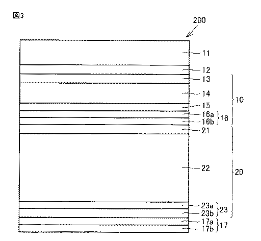
表1からわかるように、界面制御層における価電子帯上端のエネルギー準位Evおよび伝導帯下端のエネルギー準位Ecについて、裏面側表面近傍の方が光入射側表面近傍より深い準位となっていた。   As can be seen from Table 1, the energy level Ev at the top of the valence band and the energy level Ec at the bottom of the conduction band in the interface control layer are deeper in the vicinity of the back surface side than in the vicinity of the light incident surface. It was.

(電気特性の評価)
実施例1および比較例1の電気特性を測定した。測定条件としては、分光分布AM1.5、100mW/cmの光強度で照射し、測定温度を25℃とした。表2に測定結果を示す。
(Evaluation of electrical characteristics)
The electrical characteristics of Example 1 and Comparative Example 1 were measured. The measurement conditions were a spectral distribution AM1.5, irradiation with a light intensity of 100 mW / cm 2 , and a measurement temperature of 25 ° C. Table 2 shows the measurement results.

Figure 2014072200
Figure 2014072200

表2に示すように、界面制御層15を形成した実施例1では、界面制御層を有さない比較例1と比較して、短絡電流密度、開放電圧がともに向上した。すなわち、酸素および炭素を含む界面制御層15により、短絡電流、開放電圧がともに向上したことがわかる。   As shown in Table 2, in Example 1 in which the interface control layer 15 was formed, both the short-circuit current density and the open-circuit voltage were improved as compared with Comparative Example 1 having no interface control layer. That is, it can be seen that the short circuit current and the open circuit voltage are both improved by the interface control layer 15 containing oxygen and carbon.

これは、界面制御層がi型非晶質シリコンカーバイド半導体層に比べて、フェルミ準位Efが同程度で、バンドギャップEgが同程度であるにも関わらず、伝導帯の下端のエネルギー準位Ecおよび価電子帯の上端のエネルギー準位Evが相対的に深くなっているため、正孔のn型シリコン系半導体層側への拡散が低減され逆方向飽和電流が改善するために特性が向上したと考えられる。   This is because the interface control layer has the same Fermi level Ef and the same band gap Eg as the i-type amorphous silicon carbide semiconductor layer, but the energy level at the lower end of the conduction band. Since the energy level Ev at the top of Ec and the valence band is relatively deep, the diffusion of holes to the n-type silicon-based semiconductor layer side is reduced and the reverse saturation current is improved, improving the characteristics It is thought that.

[実施例2、比較例2]
(光電変換装置の構成)
実施例2として、図1に示す第1の実施形態の光電変換装置100と同様の構成を有する光電変換装置を作製した。実施例2のi型非晶質シリコンカーバイド半導体層14の膜厚を320nm、界面制御層15の膜厚を50nmとした。また、比較例2として、i型非晶質シリコンカーバイド半導体層14の膜厚を370nmとし、界面制御層を形成しない点のみ実施例2と異なる光電変換装置を作製した。なお、実施例2の界面制御層はi型であるため、i型層のトータル膜厚は実施例2は370nm、比較例2は370nmで同じである。
[Example 2, Comparative Example 2]
(Configuration of photoelectric conversion device)
As Example 2, a photoelectric conversion device having the same configuration as that of the photoelectric conversion device 100 of the first embodiment shown in FIG. 1 was produced. The film thickness of the i-type amorphous silicon carbide semiconductor layer 14 of Example 2 was 320 nm, and the film thickness of the interface control layer 15 was 50 nm. Further, as Comparative Example 2, a photoelectric conversion device different from Example 2 was manufactured only in that the thickness of the i-type amorphous silicon carbide semiconductor layer 14 was 370 nm and the interface control layer was not formed. Since the interface control layer of Example 2 is i-type, the total film thickness of the i-type layer is 370 nm in Example 2 and 370 nm in Comparative Example 2.

(光電変換装置の製造)
SnO膜を第1導電層12として備えたガラス製の基板11(アサヒガラス社製asahi-VU基板)に、第1の実施形態の製造方法にしたがい、マルチチャンバ方式のプラズマCVD装置を用いて第1光電変換層10を形成した。
(Manufacture of photoelectric conversion devices)
A multi-chamber plasma CVD apparatus is used on a glass substrate 11 (Asahi-VU substrate manufactured by Asahi Glass Co., Ltd.) having a SnO 2 film as the first conductive layer 12 according to the manufacturing method of the first embodiment. A first photoelectric conversion layer 10 was formed.

まず、p型シリコン系半導体層13を以下のように形成した。第1の反応室4内を1×10⁻⁶Torrまで排気し、基板11の温度を200℃に設定した。反応室4内に流量コントローラーによって混合ガスを導入し、排気系に設けられたコンダクションバルブにより反応室4内の圧力を一定に保った。反応室4内の圧力は、0.22Torrとした。混合ガスとして、シランガス、水素ガス、メタンガスおよびジボランガスを用いた。上記混合ガスを導入して反応室4内の圧力が安定した後、カソード電極3に27.12MHzの交流電力を投入し、カソード電極3とアノード電極2の間にプラズマを発生させた。プラズマは間欠プラズマとした。カソード電極3の単位面積あたりの電力密度は、0.22W/cmとした。形成されたp型シリコン系半導体層13の層厚は8nmであった。 First, the p-type silicon-based semiconductor layer 13 was formed as follows. The inside of the first reaction chamber 4 was evacuated to 1 × 10 −6 Torr, and the temperature of the substrate 11 was set to 200 ° C. The mixed gas was introduced into the reaction chamber 4 by a flow rate controller, and the pressure in the reaction chamber 4 was kept constant by a conduction valve provided in the exhaust system. The pressure in the reaction chamber 4 was 0.22 Torr. Silane gas, hydrogen gas, methane gas, and diborane gas were used as the mixed gas. After the mixed gas was introduced and the pressure in the reaction chamber 4 was stabilized, 27.12 MHz AC power was supplied to the cathode electrode 3 to generate plasma between the cathode electrode 3 and the anode electrode 2. The plasma was intermittent plasma. The power density per unit area of the cathode electrode 3 was 0.22 W / cm 2 . The thickness of the formed p-type silicon-based semiconductor layer 13 was 8 nm.

次に、i型非晶質シリコンカーバイド半導体層14を以下のように形成した。第2の反応室4内の圧力を0.20Torrとした。混合ガスとして、シランガス、メタンガス、水素ガスを用いた。シランガスの単位時間当たりの供給量に対するメタンガスの単位時間当たりの供給量を59体積%とした。上記混合ガスを導入して反応室4内の圧力が安定した後、カソード電極3に27.12MHzの交流電力を投入し、カソード電極3とアノード電極2との間にプラズマを発生させた。プラズマは間欠プラズマとした。カソード電極3の単位面積あたりの電力密度は、0.05W/cmとした。形成されたi型非晶質シリコンカーバイド半導体層14の層厚は320nmであった。また、バンドギャップEgは1.95eVであった。なお、バンドギャップEgは単層の透過反射測定から、タウツプロットを用いて算出した。 Next, the i-type amorphous silicon carbide semiconductor layer 14 was formed as follows. The pressure in the second reaction chamber 4 was 0.20 Torr. Silane gas, methane gas, and hydrogen gas were used as the mixed gas. The supply amount per unit time of methane gas with respect to the supply amount per unit time of silane gas was set to 59% by volume. After the mixed gas was introduced and the pressure in the reaction chamber 4 was stabilized, 27.12 MHz AC power was supplied to the cathode electrode 3 to generate plasma between the cathode electrode 3 and the anode electrode 2. The plasma was intermittent plasma. The power density per unit area of the cathode electrode 3 was 0.05 W / cm 2 . The thickness of the formed i-type amorphous silicon carbide semiconductor layer 14 was 320 nm. The band gap Eg was 1.95 eV. The band gap Eg was calculated from single layer transmission / reflection measurements using a tautu plot.

次に、界面制御層15を以下のように形成した。なお、i型非晶質シリコンカーバイド半導体層14および界面制御層15は、同じ反応室内で連続的に製膜した。第2の反応室4内の圧力は0.20Torrとした。カソード電極3に27.12MHzの交流電力を投入し、カソード電極3とアノード電極2との間にプラズマを発生させた。プラズマは間欠プラズマとし、カソード電極3の単位面積あたりの電力密度は、0.50W/cmとした。混合ガスとして、シランガス、メタンガス、水素ガス、二酸化炭素ガスを含む混合ガスを用いた。最初は、混合ガスとしてシランガス、水素ガス、メタンガスのみからなるガスを用い二酸化炭素ガスは供給しなかった。メタンガスの単位時間当たりの供給体積はシランガスの単位時間当たりの供給体積の59%であった。その後、シランガスの単位時間の供給体積に対する二酸化炭素ガスの単位時間当たりの供給体積の比率を連続的に上げていき、二酸化炭素ガスの単位時間当たりの供給体積がシランガスの単位時間当たりの供給体積の67%になるまで上げた。同時にメタンガスについて、シランガスの単位時間当たりの供給体積に対するメタンガスの単位時間当たりの供給体積の割合を連続的に少なくし供給量を0として界面制御層15を形成した。界面制御層15を形成した。このように形成することにより、光入射側が最もバンドギャップが小さく、裏面側(第2導電層17側)が最もバンドギャップの大きいグレーディッド構造を形成した。光入射側のバンドギャップEg(最小バンドギャップEg)は1.95eV、第2導電層17側のバンドギャップEg(最大バンドギャップEg)は1.99eVであった。形成された界面制御層15の層厚は50nmであった。 Next, the interface control layer 15 was formed as follows. The i-type amorphous silicon carbide semiconductor layer 14 and the interface control layer 15 were continuously formed in the same reaction chamber. The pressure in the second reaction chamber 4 was 0.20 Torr. 27.12 MHz AC power was applied to the cathode electrode 3 to generate plasma between the cathode electrode 3 and the anode electrode 2. The plasma was intermittent plasma, and the power density per unit area of the cathode electrode 3 was 0.50 W / cm 2 . As a mixed gas, a mixed gas containing silane gas, methane gas, hydrogen gas, and carbon dioxide gas was used. Initially, a gas consisting only of silane gas, hydrogen gas, and methane gas was used as a mixed gas, and carbon dioxide gas was not supplied. The supply volume per unit time of methane gas was 59% of the supply volume per unit time of silane gas. Subsequently, the ratio of the supply volume per unit time of carbon dioxide gas to the supply volume of silane gas per unit time is continuously increased, and the supply volume per unit time of carbon dioxide gas is equal to the supply volume per unit time of silane gas. Increased to 67%. At the same time, for the methane gas, the ratio of the supply volume per unit time of the methane gas to the supply volume per unit time of the silane gas was continuously reduced, and the supply amount was set to 0 to form the interface control layer 15. An interface control layer 15 was formed. By forming in this way, a graded structure having the smallest band gap on the light incident side and the largest band gap on the back surface side (second conductive layer 17 side) was formed. The band gap Eg (minimum band gap Eg) on the light incident side was 1.95 eV, and the band gap Eg (maximum band gap Eg) on the second conductive layer 17 side was 1.99 eV. The thickness of the formed interface control layer 15 was 50 nm.

次に、n型シリコン系半導体層16を以下のように形成した。第3の反応室4内の圧力を0.22Torrとした。混合ガスとして、シランガス、ホスフィンガスを含む混合ガスを使用した。上記混合ガスを導入して反応室4内の圧力が安定した後、カソード電極3に13.56MHzの交流電力を投入し、カソード電極3とアノード電極2との間にプラズマを発生させた。カソード電極3の単位面積あたりの電力密度は、0.05W/cmとした。形成されたn型シリコン系半導体層16の層厚は20nmであった。 Next, the n-type silicon-based semiconductor layer 16 was formed as follows. The pressure in the third reaction chamber 4 was 0.22 Torr. A mixed gas containing silane gas and phosphine gas was used as the mixed gas. After introducing the mixed gas and stabilizing the pressure in the reaction chamber 4, AC power of 13.56 MHz was supplied to the cathode electrode 3 to generate plasma between the cathode electrode 3 and the anode electrode 2. The power density per unit area of the cathode electrode 3 was 0.05 W / cm 2 . The layer thickness of the formed n-type silicon-based semiconductor layer 16 was 20 nm.

次に第2導電層17を以下のように形成した。第2導電層17は、透明導電膜17aと金属膜17bとからなり、これらを順次形成した。透明導電膜17aとして、マグネトロンスパッタリング法により80nmのZnO膜を形成し、金属膜17bとして、マグネトロンスパッタリング法により、120nmの銀層を積層した。このようにして、実施例2のスーパーストレート型の光電変換装置100を作製した。   Next, the second conductive layer 17 was formed as follows. The second conductive layer 17 was composed of a transparent conductive film 17a and a metal film 17b, which were sequentially formed. A 80 nm ZnO film was formed as the transparent conductive film 17a by magnetron sputtering, and a 120 nm silver layer was stacked as the metal film 17b by magnetron sputtering. In this manner, a super straight type photoelectric conversion device 100 of Example 2 was produced.

比較例2の光電変換装置として、i型非晶質シリコンカーバイド半導体層14の層厚を370nmとし、界面制御層を形成しない点のみ実施例2と異なる光電変換装置を作製した。   As a photoelectric conversion device of Comparative Example 2, a photoelectric conversion device different from that of Example 2 was produced only in that the i-type amorphous silicon carbide semiconductor layer 14 had a thickness of 370 nm and no interface control layer was formed.

(酸素濃度、炭素濃度の測定)
実施例2の光電変換装置について、第2導電層17を薬液でエッチングしたのち、二次イオン質量分析(SIMS)により層厚方向の酸素濃度および炭素濃度を測定した。図5は、実施例2の測定結果を示す。図5において、横軸は層厚方向の距離(深さ)、縦軸は原子濃度を表す。なお、本測定において、一次イオンビームの加速電圧は5.0kV、検出領域は36×36μmとした。また一次イオンビームはn型シリコン系半導体層16の裏面側(第2導電層17側)から入射した。図4において、深さ0nmは、n型シリコン系半導体層16が第2導電層17と接触していた位置であり、深さの値は、深さ0nmの位置から基板11側に向かう層厚方向の距離を表し、深さの値が大きい程、基板11(光入射側)に近い位置を示す。
(Measurement of oxygen concentration and carbon concentration)
About the photoelectric conversion apparatus of Example 2, after etching the 2nd conductive layer 17 with a chemical | medical solution, the oxygen concentration and carbon concentration of the layer thickness direction were measured by secondary ion mass spectrometry (SIMS). FIG. 5 shows the measurement results of Example 2. In FIG. 5, the horizontal axis represents the distance (depth) in the layer thickness direction, and the vertical axis represents the atomic concentration. In this measurement, the acceleration voltage of the primary ion beam was 5.0 kV, and the detection area was 36 × 36 μm 2 . The primary ion beam was incident from the back side (second conductive layer 17 side) of the n-type silicon-based semiconductor layer 16. In FIG. 4, the depth of 0 nm is the position where the n-type silicon-based semiconductor layer 16 is in contact with the second conductive layer 17, and the depth value is the layer thickness from the position of the depth of 0 nm toward the substrate 11 side. The distance in the direction is expressed, and the larger the depth value, the closer to the substrate 11 (light incident side).

図5からわかるように、実施例2おいて、第2導電層17側(裏面側)に近い領域では、酸素濃度が第2導電層17側(裏面側)の方向に進むにつれて上昇する傾向を示している。これは、裏面側の表面酸化膜からの酸素の押し込みによるものであると解される。また、基板11として使用したアサヒガラス社製のasahi-VU基板の第1導電層12が設けられている側の表面は、テクスチャ構造が形成されており、そのラフネスはおよそ50〜200nmであった。この基板11に第1光電変換層10を製膜しても、その表面には依然として50〜200nmのラフネスが残ると解される。したがって、SIMS測定における上記の検出領域では、複数のテクスチャ粒子を含むため、図5に示すピークは、実際よりもブロードな信号として測定されたと解される。   As can be seen from FIG. 5, in Example 2, in the region close to the second conductive layer 17 side (back side), the oxygen concentration tends to increase as it proceeds in the direction of the second conductive layer 17 side (back side). Show. This is understood to be due to the indentation of oxygen from the surface oxide film on the back surface side. Further, the surface of the Asahi-VU substrate manufactured by Asahi Glass Co., Ltd. used as the substrate 11 on the side where the first conductive layer 12 is provided has a texture structure, and its roughness is about 50 to 200 nm. . Even when the first photoelectric conversion layer 10 is formed on the substrate 11, it is understood that the roughness of 50 to 200 nm still remains on the surface. Therefore, since the detection region in the SIMS measurement includes a plurality of texture particles, it is understood that the peak shown in FIG. 5 is measured as a broader signal than actual.

図5においては、深さ33nm付近(界面制御層15)で酸素濃度が極大値をとった。図5に示す実施例2では、n型シリコン系半導体層16を20nm、界面制御層15を50nmの層厚で製膜したので、深さ33nm付近はちょうど界面制御層15の位置と対応している。したがって、実施例2において、酸素濃度が極大値をとる部位は、界面制御層15に含まれているとみなすことができる。界面制御層15における酸素濃度の極大値は4.3×10²¹(atoms/cm)であった。また、その時の炭素濃度は4.3×1020(atoms/cm)であった。 In FIG. 5, the oxygen concentration has a local maximum at a depth of about 33 nm (interface control layer 15). In Example 2 shown in FIG. 5, since the n-type silicon-based semiconductor layer 16 is formed with a thickness of 20 nm and the interface control layer 15 is formed with a thickness of 50 nm, the vicinity of the depth of 33 nm corresponds to the position of the interface control layer 15. Yes. Therefore, in Example 2, it can be considered that the part where the oxygen concentration has the maximum value is included in the interface control layer 15. The maximum value of the oxygen concentration in the interface control layer 15 was 4.3 × 10 21 (atoms / cm 3 ). The carbon concentration at that time was 4.3 × 10 20 (atoms / cm 3 ).

(エネルギー準位の測定)
下記の手法を用いて、実施例2のi型非晶質シリコンカーバイド半導体層14および界面制御層15のエネルギー準位を算出した。なお、すべてのエネルギー準位は真空準位を0eVとしている。価電子帯の上端のエネルギー準位Evを大気中光電子分光装置(商品名:AC−3、理研計器製製)を用いて測定した。また、伝導帯の下端のエネルギー準位Ecを価電子帯の上端のエネルギー準位Evとタウツプロットから求めたバンドギャップEgから算出した。また、フェルミ準位Efをフェルミ準位測定器(商品名:FAC−2、理研計器製)を用いて測定した。
(Measurement of energy level)
The energy levels of the i-type amorphous silicon carbide semiconductor layer 14 and the interface control layer 15 of Example 2 were calculated using the following method. Note that all energy levels have a vacuum level of 0 eV. The energy level Ev at the upper end of the valence band was measured using an atmospheric photoelectron spectrometer (trade name: AC-3, manufactured by Riken Keiki Co., Ltd.). Further, the energy level Ec at the lower end of the conduction band was calculated from the energy level Ev at the upper end of the valence band and the band gap Eg obtained from the Tautz plot. The Fermi level Ef was measured using a Fermi level measuring device (trade name: FAC-2, manufactured by Riken Keiki Co., Ltd.).

実施例2の光電変換装置のi型非晶質シリコンカーバイド半導体層、および界面制御層の光入射側表面近傍と裏面側表面近傍の各エネルギー準位を表3に示す。   Table 3 shows energy levels of the i-type amorphous silicon carbide semiconductor layer and the interface control layer of the photoelectric conversion device of Example 2 near the light incident surface and near the back surface.

Figure 2014072200
Figure 2014072200

表3からわかるように、界面制御層における価電子帯上端のエネルギー準位Evおよび伝導帯下端のエネルギー準位Ecについて、裏面側表面近傍の方が光入射側表面近傍より深い準位となっていた。   As can be seen from Table 3, the energy level Ev at the top of the valence band and the energy level Ec at the bottom of the conduction band in the interface control layer are deeper in the vicinity of the back surface side than in the vicinity of the light incident surface. It was.

(電気特性の評価)
実施例2および比較例2の電気特性を測定した。測定条件としては、分光分布AM1.5、100mW/cmの光強度で照射し、測定温度を25℃とした。表4に測定結果を示す。
(Evaluation of electrical characteristics)
The electrical characteristics of Example 2 and Comparative Example 2 were measured. The measurement conditions were a spectral distribution AM1.5, irradiation with a light intensity of 100 mW / cm 2 , and a measurement temperature of 25 ° C. Table 4 shows the measurement results.

Figure 2014072200
Figure 2014072200

表2に示すように、界面制御層15を形成した実施例2では、界面制御層を有さない比較例2と比較して、開放電圧が向上した。すなわち、酸素および炭素を含む界面制御層15により、開放電圧が向上したことがわかる。   As shown in Table 2, in Example 2 in which the interface control layer 15 was formed, the open-circuit voltage was improved as compared with Comparative Example 2 having no interface control layer. That is, it can be seen that the open circuit voltage is improved by the interface control layer 15 containing oxygen and carbon.

これは、界面制御層がi型非晶質シリコンカーバイド半導体層に比べて、フェルミ準位Efが同程度で、バンドギャップEgが少し広くなっている程度であるにも関わらず、伝導帯の下端のエネルギー準位Ecおよび価電子帯の上端のエネルギー準位Evが相対的に深くなっているため、正孔のn型シリコン系半導体層側への拡散が低減され逆方向飽和電流が改善するために特性が向上したと考えられる。   This is because the interface control layer has the same Fermi level Ef and a slightly larger band gap Eg than the i-type amorphous silicon carbide semiconductor layer, but the lower end of the conduction band. Since the energy level Ec and the energy level Ev at the upper end of the valence band are relatively deep, the diffusion of holes to the n-type silicon-based semiconductor layer side is reduced and the reverse saturation current is improved. It is thought that the characteristics were improved.

1 ヒーター、2 アノード電極、3 カソード電極、4 反応室、5 マッチング回路、6 高周波電源、10 第1光電変換層、11 基板、12 第1導電層、13 p型シリコン系半導体層、14 i型非晶質シリコンカーバイド半導体層、15 界面制御層、16 n型シリコン系半導体層、16a n型非晶質シリコン層、16b n型微結晶シリコン層、17 第2導電層、17a 透明導電膜、17b 金属膜、20 第2光電変換層、21 p型シリコン系半導体層、22 i型シリコン系半導体層、23 n型シリコン系半導体層、23a n型非晶質シリコン系半導体層、23b n型微結晶シリコン系半導体層、100,200 光電変換装置。   DESCRIPTION OF SYMBOLS 1 Heater, 2 Anode electrode, 3 Cathode electrode, 4 Reaction chamber, 5 Matching circuit, 6 High frequency power supply, 10 1st photoelectric converting layer, 11 board | substrate, 12 1st conductive layer, 13 p-type silicon type semiconductor layer, 14 i type Amorphous silicon carbide semiconductor layer, 15 interface control layer, 16 n-type silicon-based semiconductor layer, 16a n-type amorphous silicon layer, 16b n-type microcrystalline silicon layer, 17 second conductive layer, 17a transparent conductive film, 17b Metal film, 20 second photoelectric conversion layer, 21 p-type silicon-based semiconductor layer, 22 i-type silicon-based semiconductor layer, 23 n-type silicon-based semiconductor layer, 23a n-type amorphous silicon-based semiconductor layer, 23b n-type microcrystal Silicon-based semiconductor layer, 100, 200 photoelectric conversion device.

Claims (5)

第1導電層、第1光電変換層と、第2導電層がこの順で積層されてなる光電変換装置であって、
前記第1光電変換層は、前記第1導電層側から前記第2導電層側に向けて順に積層された、p型シリコン系半導体層と、i型非晶質シリコンカーバイド半導体層と、界面制御層と、n型シリコン系半導体層と、を有し、
前記界面制御層は、シリコン原子、炭素原子および酸素原子を含む、光電変換装置。
A photoelectric conversion device in which a first conductive layer, a first photoelectric conversion layer, and a second conductive layer are laminated in this order,
The first photoelectric conversion layer includes a p-type silicon-based semiconductor layer, an i-type amorphous silicon carbide semiconductor layer, and an interface control, which are sequentially stacked from the first conductive layer side to the second conductive layer side. A layer and an n-type silicon-based semiconductor layer,
The said interface control layer is a photoelectric conversion apparatus containing a silicon atom, a carbon atom, and an oxygen atom.
前記界面制御層の酸素濃度は、1×10²⁰(atoms/cm)以上1×1022(atoms/cm)以下である、請求項1に記載の光電変換装置。 2. The photoelectric conversion device according to claim 1, wherein an oxygen concentration of the interface control layer is 1 × 10 20 (atoms / cm 3 ) or more and 1 × 10 22 (atoms / cm 3 ) or less. 前記界面制御層において、層厚方向の酸素濃度の極大値を有する、請求項1または2に記載の光電変換装置。   The photoelectric conversion device according to claim 1, wherein the interface control layer has a maximum value of oxygen concentration in a layer thickness direction. 前記界面制御層の炭素濃度は、1×10²⁰(atoms/cm)以上2×1021(atoms/cm)以下である、請求項1〜3のいずれかに記載の光電変換装置。 The photoelectric conversion device according to claim 1, wherein a carbon concentration of the interface control layer is 1 × 10 20 (atoms / cm 3 ) or more and 2 × 10 21 (atoms / cm 3 ) or less. 請求項1に記載の光電変換装置の製造方法であって、
シリコン原子、炭素原子および酸素原子を含むガスを供給して前記界面制御層を形成する工程を有する、光電変換装置の製造方法。
It is a manufacturing method of the photoelectric conversion device according to claim 1,
A method for manufacturing a photoelectric conversion device, comprising a step of supplying a gas containing silicon atoms, carbon atoms, and oxygen atoms to form the interface control layer.
JP2012214347A 2012-09-27 2012-09-27 Photoelectric conversion device and method of manufacturing the same Pending JP2014072200A (en)

Priority Applications (1)

Application Number Priority Date Filing Date Title
JP2012214347A JP2014072200A (en) 2012-09-27 2012-09-27 Photoelectric conversion device and method of manufacturing the same

Applications Claiming Priority (1)

Application Number Priority Date Filing Date Title
JP2012214347A JP2014072200A (en) 2012-09-27 2012-09-27 Photoelectric conversion device and method of manufacturing the same

Publications (1)

Publication Number Publication Date
JP2014072200A true JP2014072200A (en) 2014-04-21

Family

ID=50747190

Family Applications (1)

Application Number Title Priority Date Filing Date
JP2012214347A Pending JP2014072200A (en) 2012-09-27 2012-09-27 Photoelectric conversion device and method of manufacturing the same

Country Status (1)

Country Link
JP (1) JP2014072200A (en)

Similar Documents

Publication Publication Date Title
Lambertz et al. Microcrystalline silicon–oxygen alloys for application in silicon solar cells and modules
JP4257332B2 (en) Silicon-based thin film solar cell
US20050205127A1 (en) Photovoltaic device
JP4411338B2 (en) Thin film solar cell module
US20130061915A1 (en) Thin film solar cells and manufacturing method thereof
JP2009177225A (en) Thin film solar cell module
US20100163100A1 (en) Photovoltaic Device and Process for Producing Same
WO2006057160A1 (en) Thin film photoelectric converter
JP4459086B2 (en) Laminated photovoltaic device and manufacturing method thereof
JP2010283161A (en) Solar cell and manufacturing method thereof
CN101246926A (en) Amorphous boron-carbon alloy and photovoltaic application thereof
JP2009290115A (en) Silicon-based thin-film solar battery
JP5770294B2 (en) Photoelectric conversion device and manufacturing method thereof
JP2016131165A (en) Solar cell and manufacturing method thereof
CN103238219A (en) Improved alpha-Si:H absorber layer for alpha-Si single- and multijunction thin film silicon solar cell
JP4443274B2 (en) Photoelectric conversion device
CN103430326A (en) SiOxN layer of microcrystalline PIN junction
JP2011014618A (en) Solar cell and method of manufacturing the same
Zhang et al. Micromorph tandem solar cells: optimization of the microcrystalline silicon bottom cell in a single chamber system
JP2014072200A (en) Photoelectric conversion device and method of manufacturing the same
JP2014072199A (en) Photoelectric conversion device and method of manufacturing the same
Walder et al. Amorphous silicon oxinitride in silicon thin-film solar cells
JP4642126B2 (en) Laminated photovoltaic device and method for producing laminated photovoltaic device
JP2010283162A (en) Solar cell and manufacturing method thereof
JP2006120712A (en) Thin film photoelectric converter and manufacturing method therefor