JP2013143563A - Systems for assembling electronic devices with internal moisture-resistant coatings - Google Patents
Systems for assembling electronic devices with internal moisture-resistant coatings Download PDFInfo
- Publication number
- JP2013143563A JP2013143563A JP2012096417A JP2012096417A JP2013143563A JP 2013143563 A JP2013143563 A JP 2013143563A JP 2012096417 A JP2012096417 A JP 2012096417A JP 2012096417 A JP2012096417 A JP 2012096417A JP 2013143563 A JP2013143563 A JP 2013143563A
- Authority
- JP
- Japan
- Prior art keywords
- assembly
- coating
- component
- electronic device
- water
- Prior art date
- Legal status (The legal status is an assumption and is not a legal conclusion. Google has not performed a legal analysis and makes no representation as to the accuracy of the status listed.)
- Pending
Links
- 238000000576 coating method Methods 0.000 title claims abstract description 179
- 239000011248 coating agent Substances 0.000 claims abstract description 173
- 238000000034 method Methods 0.000 claims abstract description 22
- XLYOFNOQVPJJNP-UHFFFAOYSA-N water Substances O XLYOFNOQVPJJNP-UHFFFAOYSA-N 0.000 claims description 124
- 239000000463 material Substances 0.000 claims description 35
- 239000000047 product Substances 0.000 claims description 16
- 230000000873 masking effect Effects 0.000 claims description 15
- 238000004381 surface treatment Methods 0.000 claims description 10
- 238000007689 inspection Methods 0.000 claims description 6
- 238000004891 communication Methods 0.000 claims description 4
- 229920000052 poly(p-xylylene) Polymers 0.000 claims description 4
- 238000005516 engineering process Methods 0.000 claims description 3
- 238000011144 upstream manufacturing Methods 0.000 claims description 3
- 238000009792 diffusion process Methods 0.000 claims description 2
- 229920000642 polymer Polymers 0.000 claims description 2
- 239000002904 solvent Substances 0.000 claims description 2
- 238000000151 deposition Methods 0.000 claims 3
- OOLUVSIJOMLOCB-UHFFFAOYSA-N 1633-22-3 Chemical compound C1CC(C=C2)=CC=C2CCC2=CC=C1C=C2 OOLUVSIJOMLOCB-UHFFFAOYSA-N 0.000 claims 2
- 230000008021 deposition Effects 0.000 claims 2
- 239000013067 intermediate product Substances 0.000 claims 2
- NRNFFDZCBYOZJY-UHFFFAOYSA-N p-quinodimethane Chemical group C=C1C=CC(=C)C=C1 NRNFFDZCBYOZJY-UHFFFAOYSA-N 0.000 claims 1
- 230000000379 polymerizing effect Effects 0.000 claims 1
- 125000006839 xylylene group Chemical group 0.000 claims 1
- 229910000679 solder Inorganic materials 0.000 description 11
- 230000007246 mechanism Effects 0.000 description 8
- 238000004140 cleaning Methods 0.000 description 6
- 239000004020 conductor Substances 0.000 description 6
- 230000008878 coupling Effects 0.000 description 6
- 238000010168 coupling process Methods 0.000 description 6
- 238000005859 coupling reaction Methods 0.000 description 6
- 230000004907 flux Effects 0.000 description 6
- 239000004065 semiconductor Substances 0.000 description 6
- 238000005476 soldering Methods 0.000 description 6
- 239000000356 contaminant Substances 0.000 description 5
- 230000032258 transport Effects 0.000 description 5
- 238000005229 chemical vapour deposition Methods 0.000 description 4
- 230000008569 process Effects 0.000 description 4
- 230000009931 harmful effect Effects 0.000 description 3
- 238000009434 installation Methods 0.000 description 3
- 238000004519 manufacturing process Methods 0.000 description 3
- 230000013011 mating Effects 0.000 description 3
- 238000005240 physical vapour deposition Methods 0.000 description 3
- 238000007639 printing Methods 0.000 description 3
- 238000012545 processing Methods 0.000 description 3
- 238000012546 transfer Methods 0.000 description 3
- VRBFTYUMFJWSJY-UHFFFAOYSA-N 28804-46-8 Chemical compound ClC1CC(C=C2)=CC=C2C(Cl)CC2=CC=C1C=C2 VRBFTYUMFJWSJY-UHFFFAOYSA-N 0.000 description 2
- 239000003990 capacitor Substances 0.000 description 2
- 238000007650 screen-printing Methods 0.000 description 2
- 238000004528 spin coating Methods 0.000 description 2
- 238000005507 spraying Methods 0.000 description 2
- 239000000758 substrate Substances 0.000 description 2
- 239000002982 water resistant material Substances 0.000 description 2
- 241000280258 Dyschoriste linearis Species 0.000 description 1
- 239000004593 Epoxy Substances 0.000 description 1
- 240000002853 Nelumbo nucifera Species 0.000 description 1
- 235000006508 Nelumbo nucifera Nutrition 0.000 description 1
- 235000006510 Nelumbo pentapetala Nutrition 0.000 description 1
- 238000007792 addition Methods 0.000 description 1
- 230000002411 adverse Effects 0.000 description 1
- 229910045601 alloy Inorganic materials 0.000 description 1
- 239000000956 alloy Substances 0.000 description 1
- 229910052782 aluminium Inorganic materials 0.000 description 1
- XAGFODPZIPBFFR-UHFFFAOYSA-N aluminium Chemical compound [Al] XAGFODPZIPBFFR-UHFFFAOYSA-N 0.000 description 1
- 238000004458 analytical method Methods 0.000 description 1
- 230000002547 anomalous effect Effects 0.000 description 1
- 230000001680 brushing effect Effects 0.000 description 1
- 150000001875 compounds Chemical class 0.000 description 1
- 238000005260 corrosion Methods 0.000 description 1
- 230000007797 corrosion Effects 0.000 description 1
- 238000005520 cutting process Methods 0.000 description 1
- 238000007872 degassing Methods 0.000 description 1
- 238000005238 degreasing Methods 0.000 description 1
- 238000012217 deletion Methods 0.000 description 1
- 230000037430 deletion Effects 0.000 description 1
- 238000005137 deposition process Methods 0.000 description 1
- 238000010586 diagram Methods 0.000 description 1
- 238000001035 drying Methods 0.000 description 1
- 238000005441 electronic device fabrication Methods 0.000 description 1
- 125000003700 epoxy group Chemical group 0.000 description 1
- 238000005530 etching Methods 0.000 description 1
- 238000001704 evaporation Methods 0.000 description 1
- 230000008020 evaporation Effects 0.000 description 1
- PCHJSUWPFVWCPO-UHFFFAOYSA-N gold Chemical compound [Au] PCHJSUWPFVWCPO-UHFFFAOYSA-N 0.000 description 1
- 229910052737 gold Inorganic materials 0.000 description 1
- 239000010931 gold Substances 0.000 description 1
- 230000002209 hydrophobic effect Effects 0.000 description 1
- 230000005661 hydrophobic surface Effects 0.000 description 1
- 230000001788 irregular Effects 0.000 description 1
- 238000000608 laser ablation Methods 0.000 description 1
- 239000012528 membrane Substances 0.000 description 1
- 229910052751 metal Inorganic materials 0.000 description 1
- 239000002184 metal Substances 0.000 description 1
- 150000002739 metals Chemical class 0.000 description 1
- 238000012986 modification Methods 0.000 description 1
- 230000004048 modification Effects 0.000 description 1
- 239000000178 monomer Substances 0.000 description 1
- 230000003647 oxidation Effects 0.000 description 1
- 238000007254 oxidation reaction Methods 0.000 description 1
- 239000012466 permeate Substances 0.000 description 1
- 238000000623 plasma-assisted chemical vapour deposition Methods 0.000 description 1
- 238000005498 polishing Methods 0.000 description 1
- -1 poly (p-xylylene) Polymers 0.000 description 1
- 229920000647 polyepoxide Polymers 0.000 description 1
- 239000002243 precursor Substances 0.000 description 1
- 238000004549 pulsed laser deposition Methods 0.000 description 1
- 230000005855 radiation Effects 0.000 description 1
- 238000011084 recovery Methods 0.000 description 1
- 238000004544 sputter deposition Methods 0.000 description 1
- 230000003068 static effect Effects 0.000 description 1
- 230000003075 superhydrophobic effect Effects 0.000 description 1
- 230000001360 synchronised effect Effects 0.000 description 1
- 238000002207 thermal evaporation Methods 0.000 description 1
- 239000012815 thermoplastic material Substances 0.000 description 1
- 229920001187 thermosetting polymer Polymers 0.000 description 1
- 238000007740 vapor deposition Methods 0.000 description 1
- 238000009834 vaporization Methods 0.000 description 1
- 230000008016 vaporization Effects 0.000 description 1
Images


Classifications
-
- H—ELECTRICITY
- H05—ELECTRIC TECHNIQUES NOT OTHERWISE PROVIDED FOR
- H05K—PRINTED CIRCUITS; CASINGS OR CONSTRUCTIONAL DETAILS OF ELECTRIC APPARATUS; MANUFACTURE OF ASSEMBLAGES OF ELECTRICAL COMPONENTS
- H05K13/00—Apparatus or processes specially adapted for manufacturing or adjusting assemblages of electric components
- H05K13/04—Mounting of components, e.g. of leadless components
- H05K13/0495—Mounting of components, e.g. of leadless components having a plurality of work-stations
-
- H—ELECTRICITY
- H05—ELECTRIC TECHNIQUES NOT OTHERWISE PROVIDED FOR
- H05K—PRINTED CIRCUITS; CASINGS OR CONSTRUCTIONAL DETAILS OF ELECTRIC APPARATUS; MANUFACTURE OF ASSEMBLAGES OF ELECTRICAL COMPONENTS
- H05K13/00—Apparatus or processes specially adapted for manufacturing or adjusting assemblages of electric components
- H05K13/04—Mounting of components, e.g. of leadless components
-
- H—ELECTRICITY
- H05—ELECTRIC TECHNIQUES NOT OTHERWISE PROVIDED FOR
- H05K—PRINTED CIRCUITS; CASINGS OR CONSTRUCTIONAL DETAILS OF ELECTRIC APPARATUS; MANUFACTURE OF ASSEMBLAGES OF ELECTRICAL COMPONENTS
- H05K3/00—Apparatus or processes for manufacturing printed circuits
- H05K3/22—Secondary treatment of printed circuits
- H05K3/28—Applying non-metallic protective coatings
- H05K3/282—Applying non-metallic protective coatings for inhibiting the corrosion of the circuit, e.g. for preserving the solderability
-
- H—ELECTRICITY
- H05—ELECTRIC TECHNIQUES NOT OTHERWISE PROVIDED FOR
- H05K—PRINTED CIRCUITS; CASINGS OR CONSTRUCTIONAL DETAILS OF ELECTRIC APPARATUS; MANUFACTURE OF ASSEMBLAGES OF ELECTRICAL COMPONENTS
- H05K3/00—Apparatus or processes for manufacturing printed circuits
- H05K3/22—Secondary treatment of printed circuits
- H05K3/28—Applying non-metallic protective coatings
- H05K3/284—Applying non-metallic protective coatings for encapsulating mounted components
-
- C—CHEMISTRY; METALLURGY
- C08—ORGANIC MACROMOLECULAR COMPOUNDS; THEIR PREPARATION OR CHEMICAL WORKING-UP; COMPOSITIONS BASED THEREON
- C08G—MACROMOLECULAR COMPOUNDS OBTAINED OTHERWISE THAN BY REACTIONS ONLY INVOLVING UNSATURATED CARBON-TO-CARBON BONDS
- C08G61/00—Macromolecular compounds obtained by reactions forming a carbon-to-carbon link in the main chain of the macromolecule
- C08G61/02—Macromolecular compounds containing only carbon atoms in the main chain of the macromolecule, e.g. polyxylylenes
- C08G61/025—Polyxylylenes
-
- H—ELECTRICITY
- H05—ELECTRIC TECHNIQUES NOT OTHERWISE PROVIDED FOR
- H05K—PRINTED CIRCUITS; CASINGS OR CONSTRUCTIONAL DETAILS OF ELECTRIC APPARATUS; MANUFACTURE OF ASSEMBLAGES OF ELECTRICAL COMPONENTS
- H05K13/00—Apparatus or processes specially adapted for manufacturing or adjusting assemblages of electric components
- H05K13/04—Mounting of components, e.g. of leadless components
- H05K13/046—Surface mounting
- H05K13/0465—Surface mounting by soldering
-
- H—ELECTRICITY
- H05—ELECTRIC TECHNIQUES NOT OTHERWISE PROVIDED FOR
- H05K—PRINTED CIRCUITS; CASINGS OR CONSTRUCTIONAL DETAILS OF ELECTRIC APPARATUS; MANUFACTURE OF ASSEMBLAGES OF ELECTRICAL COMPONENTS
- H05K3/00—Apparatus or processes for manufacturing printed circuits
- H05K3/22—Secondary treatment of printed circuits
- H05K3/28—Applying non-metallic protective coatings
-
- H—ELECTRICITY
- H05—ELECTRIC TECHNIQUES NOT OTHERWISE PROVIDED FOR
- H05K—PRINTED CIRCUITS; CASINGS OR CONSTRUCTIONAL DETAILS OF ELECTRIC APPARATUS; MANUFACTURE OF ASSEMBLAGES OF ELECTRICAL COMPONENTS
- H05K3/00—Apparatus or processes for manufacturing printed circuits
- H05K3/30—Assembling printed circuits with electric components, e.g. with resistor
- H05K3/32—Assembling printed circuits with electric components, e.g. with resistor electrically connecting electric components or wires to printed circuits
- H05K3/34—Assembling printed circuits with electric components, e.g. with resistor electrically connecting electric components or wires to printed circuits by soldering
- H05K3/341—Surface mounted components
-
- C—CHEMISTRY; METALLURGY
- C08—ORGANIC MACROMOLECULAR COMPOUNDS; THEIR PREPARATION OR CHEMICAL WORKING-UP; COMPOSITIONS BASED THEREON
- C08G—MACROMOLECULAR COMPOUNDS OBTAINED OTHERWISE THAN BY REACTIONS ONLY INVOLVING UNSATURATED CARBON-TO-CARBON BONDS
- C08G2261/00—Macromolecular compounds obtained by reactions forming a carbon-to-carbon link in the main chain of the macromolecule
- C08G2261/30—Monomer units or repeat units incorporating structural elements in the main chain
- C08G2261/31—Monomer units or repeat units incorporating structural elements in the main chain incorporating aromatic structural elements in the main chain
- C08G2261/312—Non-condensed aromatic systems, e.g. benzene
-
- H—ELECTRICITY
- H05—ELECTRIC TECHNIQUES NOT OTHERWISE PROVIDED FOR
- H05K—PRINTED CIRCUITS; CASINGS OR CONSTRUCTIONAL DETAILS OF ELECTRIC APPARATUS; MANUFACTURE OF ASSEMBLAGES OF ELECTRICAL COMPONENTS
- H05K2203/00—Indexing scheme relating to apparatus or processes for manufacturing printed circuits covered by H05K3/00
- H05K2203/13—Moulding and encapsulation; Deposition techniques; Protective layers
- H05K2203/1333—Deposition techniques, e.g. coating
-
- Y—GENERAL TAGGING OF NEW TECHNOLOGICAL DEVELOPMENTS; GENERAL TAGGING OF CROSS-SECTIONAL TECHNOLOGIES SPANNING OVER SEVERAL SECTIONS OF THE IPC; TECHNICAL SUBJECTS COVERED BY FORMER USPC CROSS-REFERENCE ART COLLECTIONS [XRACs] AND DIGESTS
- Y10—TECHNICAL SUBJECTS COVERED BY FORMER USPC
- Y10T—TECHNICAL SUBJECTS COVERED BY FORMER US CLASSIFICATION
- Y10T29/00—Metal working
- Y10T29/49—Method of mechanical manufacture
- Y10T29/49002—Electrical device making
-
- Y—GENERAL TAGGING OF NEW TECHNOLOGICAL DEVELOPMENTS; GENERAL TAGGING OF CROSS-SECTIONAL TECHNOLOGIES SPANNING OVER SEVERAL SECTIONS OF THE IPC; TECHNICAL SUBJECTS COVERED BY FORMER USPC CROSS-REFERENCE ART COLLECTIONS [XRACs] AND DIGESTS
- Y10—TECHNICAL SUBJECTS COVERED BY FORMER USPC
- Y10T—TECHNICAL SUBJECTS COVERED BY FORMER US CLASSIFICATION
- Y10T29/00—Metal working
- Y10T29/49—Method of mechanical manufacture
- Y10T29/49826—Assembling or joining
- Y10T29/49885—Assembling or joining with coating before or during assembling
-
- Y—GENERAL TAGGING OF NEW TECHNOLOGICAL DEVELOPMENTS; GENERAL TAGGING OF CROSS-SECTIONAL TECHNOLOGIES SPANNING OVER SEVERAL SECTIONS OF THE IPC; TECHNICAL SUBJECTS COVERED BY FORMER USPC CROSS-REFERENCE ART COLLECTIONS [XRACs] AND DIGESTS
- Y10—TECHNICAL SUBJECTS COVERED BY FORMER USPC
- Y10T—TECHNICAL SUBJECTS COVERED BY FORMER US CLASSIFICATION
- Y10T29/00—Metal working
- Y10T29/53—Means to assemble or disassemble
- Y10T29/5313—Means to assemble electrical device
- Y10T29/53187—Multiple station assembly apparatus
Landscapes
- Engineering & Computer Science (AREA)
- Manufacturing & Machinery (AREA)
- Microelectronics & Electronic Packaging (AREA)
- Chemical & Material Sciences (AREA)
- Medicinal Chemistry (AREA)
- Chemical Kinetics & Catalysis (AREA)
- Health & Medical Sciences (AREA)
- Polymers & Plastics (AREA)
- Organic Chemistry (AREA)
- Non-Metallic Protective Coatings For Printed Circuits (AREA)
- Application Of Or Painting With Fluid Materials (AREA)
- Supply And Installment Of Electrical Components (AREA)
- Casings For Electric Apparatus (AREA)
Abstract
Description
[0001]本開示は、概括的には、ポータブル式家庭用電子デバイスを含め、電子デバイスを組み立てるためのシステム及び方法に、より厳密には電子デバイスに内部耐水性を付与する組立システム及び方法に関する。よりいっそう厳密には、本開示は、電子デバイスの内部表面に耐水性被覆を形成するためのシステム及び方法に関する。 [0001] The present disclosure relates generally to systems and methods for assembling electronic devices, including portable consumer electronic devices, and more specifically to assembly systems and methods for imparting internal water resistance to electronic devices. . Even more strictly, the present disclosure relates to systems and methods for forming a water-resistant coating on the inner surface of an electronic device.
[0002]様々な態様では、本開示の教示による、電子デバイスに内部耐水性を付与するためのシステムは、それぞれの電子デバイスの内部表面に耐水性被覆を塗工するための1つ又はそれ以上の要素を含んでいる。その様なシステムは、ここではより簡略に「電子デバイスを組み立てるためのシステム」又はよりいっそう簡略に「組立システム」と呼称されることもある。 [0002] In various aspects, a system for imparting internal water resistance to an electronic device according to the teachings of the present disclosure includes one or more for applying a water resistant coating to the internal surface of each electronic device. Contains the elements. Such a system may be referred to herein more simply as a “system for assembling an electronic device” or even more simply as an “assembly system”.
[0003]内部耐水性の備わった電子デバイスを組み立てるためのシステムシの或る特定の実施形態は、表面実装技術(SMT)部要素、組立部要素、及び少なくとも1つの塗被部要素を含んでいる。 [0003] Certain embodiments of a system for assembling an electronic device with internal water resistance include a surface mount technology (SMT) component element, an assembly component element, and at least one coated component element. Yes.
[0004]SMT部要素では、パッケージ化されていない半導体デバイス及び/又はパッケージ化されている半導体デバイスや他の電子的構成要素(例えば、抵抗子、コンデンサ、誘導子、トランスジューサ、モジュールなど)の様なSMTデバイスが、回路盤に電気的に結合され且つ物理的に固着される。幾つかの実施形態では、SMT部要素は自動化されており、よって、それぞれのSMTデバイスを、回路盤の適切な場所に、正しく配置させ、電気的に結合させ、且つ物理的に固着させられる装置を含んでいる。 [0004] In an SMT component, like unpackaged semiconductor devices and / or packaged semiconductor devices and other electronic components (eg, resistors, capacitors, inductors, transducers, modules, etc.) SMT devices are electrically coupled and physically secured to the circuit board. In some embodiments, the SMT components are automated, so that each SMT device is properly positioned, electrically coupled, and physically secured to the appropriate location on the circuit board. Is included.
[0005]組立部要素では、電子デバイス完成品の他の構成要素が、回路盤と一体に組み立てられる。これら他の構成要素には、様々な電子的構成要素、トランスジューサ、通信用構成要素、ユーザーインターフェース構成要素、及びハウジング又はケース構成要素を含め、電子デバイスの他の構成要素の全てが含まれる。 [0005] In the assembly element, the other components of the finished electronic device are assembled together with the circuit board. These other components include all of the other components of the electronic device, including various electronic components, transducers, communication components, user interface components, and housing or case components.
[0006]幾つかの実施形態では、組立システムは更にマスキング部要素を含んでいてもよい。マスキング部要素は、回路盤及び回路盤と一体に組み立てられた構成要素にマスクを塗工するか又はマスクを一体に組み立てるように構成されている。マスクは、耐水性被覆が、各種機構への電気接続の確立を阻害したり、各種構成要素からの熱の移動を阻害したり、各種構成要素の作動を阻害したり、或いはそれ以外に電子デバイスの性能に有害な影響を及ぼしたりするのを防止するように構成されている。 [0006] In some embodiments, the assembly system may further include a masking element. The masking element is configured to apply the mask to the circuit board and the component assembled integrally with the circuit board or to assemble the mask integrally. The mask has a water resistant coating that prevents the establishment of electrical connections to various mechanisms, inhibits the transfer of heat from various components, inhibits the operation of various components, or otherwise electronic devices It is configured to prevent harmful effects on the performance of the machine.
[0007]組立システムの塗被部要素は、電子デバイス組立途上品(又は、より簡略に「デバイス組立途上品」又は「電子的半組立品」)の少なくとも一部分に耐水性を付与するように構成されている。幾つかの実施形態では、塗被部要素は、耐水性被覆を、電子デバイス組立途上品の少なくとも幾つかの部分に、より具体的には電子デバイス組立途上品の内部の内に置かれることになる表面に、塗工することができる。塗被部要素は、耐水性被覆を非選択的に塗工するように構成されていてもよいし、耐水性被覆を電子デバイス組立途上品の選択された諸部分に塗工するように構成されていてもよい。塗被部要素は、組立システムの多数の異なった場所に組み込むことができるであろう。 [0007] The coating component of the assembly system is configured to provide water resistance to at least a portion of an electronic device assembly (or more simply "device assembly" or "electronic subassembly"). Has been. In some embodiments, the coating element has a water-resistant coating placed on at least some portion of the electronic device assembly, more specifically within the interior of the electronic device assembly. Can be applied to the resulting surface. The coated portion element may be configured to non-selectively apply the water resistant coating or may be configured to apply the water resistant coating to selected portions of the electronic device assembly. It may be. The coating element could be incorporated at a number of different locations in the assembly system.
[0008]組立システムの幾つかの実施形態は、少なくとも1つの塗被部要素をシステムのSMT部要素に組み込んでいる。他の実施形態では、塗被部要素はSMT部要素と組立部要素の間に設置されている。幾つかの実施形態では、1つ又はそれ以上の塗被部要素が組立部要素に組み込まれている。その様な実施形態では、塗被部要素は、耐水性被覆を構成要素に、それが電子デバイス組立途上品の他の構成要素と一体に組み立てられるに先立って、塗工するように構成されている場合もあれば、耐水性被覆を構成要素に、それが回路盤又は電子デバイス組立途上品の別の構成要素と一体に組み立てられてしまってから、塗工するように構成されている場合もある。 [0008] Some embodiments of the assembly system incorporate at least one coated element into the SMT component of the system. In other embodiments, the coating element is located between the SMT element and the assembly element. In some embodiments, one or more coating elements are incorporated into the assembly element. In such embodiments, the coating element is configured to be applied to the water-resistant coating on the component prior to being assembled integrally with the other components of the electronic device assembly. In other cases, the water-resistant coating may be applied to the component and then applied to the component after it has been assembled together with another component of the circuit board or electronic device assembly. is there.
[0009]多種多様な塗被部要素の1つ又はそれ以上を、電子デバイスを組み立てるためのシステムに組み入れることができるであろう。限定するわけではないが、組立システムは、化学気相堆積(CVD)やプラズマベース堆積プロセス(限定するわけではないがプラズマ強化型CVDプロセスを含む)を採用している塗被部要素、又は物理気相堆積(PVD)により耐水性被覆を塗工する塗被部要素、又は被覆材料を基板上に物理的に塗工する(例えば、吹付、回転塗布、印刷などによる)装置、を含んでいてもよい。 [0009] One or more of a wide variety of coating elements could be incorporated into a system for assembling an electronic device. An assembly system may include, but is not limited to, coating elements that employ chemical vapor deposition (CVD) or plasma-based deposition processes (including but not limited to plasma enhanced CVD processes) or physical A coating element for applying a water-resistant coating by vapor deposition (PVD), or a device for physically applying a coating material onto a substrate (eg, by spraying, spin coating, printing, etc.) Also good.
[0010]電子デバイスを組み立てるためのシステムは、塗被部要素に加えて、耐水性被覆の選択された諸部分を電子デバイス組立途上品から除去する1つ又はそれ以上の材料除去部要素を含んでいてもよい。材料除去部要素は、材料を電子デバイス組立途上品の耐水性被覆の選択された1つ又はそれ以上の諸部分から何らかの適した手段によって除去するように構成することができるであろう。限定するわけではないが、材料除去部要素は、材料を耐水性被覆のそれぞれの選択された領域から、焼灼するか、溶解させるか、気化させるか、機械的に除去するか、又はそれ以外のやり方で材料を取り去るように構成することができるであろう。 [0010] A system for assembling an electronic device includes, in addition to the coating element, one or more material removal elements that remove selected portions of the water-resistant coating from the electronic device assembly. You may go out. The material removal element could be configured to remove material from the selected one or more portions of the water resistant coating of the electronic device assembly by any suitable means. Without limitation, the material removal element can cauterize, dissolve, vaporize, mechanically remove or otherwise remove material from each selected area of the water resistant coating. It could be configured to remove material in a manner.
[0011]幾つかの実施形態では、組立システムは、塗被部要素が組立ラインの他部構成要素とインライン又はオンラインである組立ラインを備えている。他の実施形態では、塗被部要素は、組立ラインから遠隔に設置されている場合もあれば、組立ラインからオフラインに設置されている場合もある。塗被部要素をオフラインに設置させるシステムの実施形態では、塗被部要素は、組立ラインと同じ施設に設置されている。塗被部要素がインライン設置かオフライン設置かに関わりなく、組立システム又は組立ラインは、携帯電話やポータブル式メディアプレイヤーやカメラなどのポータブル式電子デバイスを含め、電子デバイスの製造用として構成されている。 [0011] In some embodiments, the assembly system comprises an assembly line in which the coated elements are inline or online with other components of the assembly line. In other embodiments, the coating element may be installed remotely from the assembly line, or may be installed offline from the assembly line. In an embodiment of the system where the coating element is installed offline, the coating element is installed in the same facility as the assembly line. Regardless of whether the coating element is installed inline or offline, the assembly system or assembly line is configured for the manufacture of electronic devices, including portable electronic devices such as mobile phones, portable media players and cameras. .
[0012]電子的組立品又は半組立品を耐水性又は防水性にさせる方法も開示されている。その様な方法は、被覆を、組立済みの電子的構成要素の少なくとも諸部分に塗工する段階を含んでいる。その様な方法は、耐水性被覆を、電子デバイス組立途上品又は半組立品に塗工する段階と、その後に少なくとも1つの構成要素を当該電子デバイス組立途上品と一体に組み立てる段階と、を含んでいる。幾つかの実施形態では、組み付けられる側の構成要素は(少なくとも組立中は)耐水性被覆を欠いている。他の実施形態では、組み付けられる側の構成要素は、電子デバイス組立途上品側の耐水性被覆と(例えば、材料、肌理、又は他の特徴が)同じ耐水性被覆を含んでいる場合もあれば、異なった耐水性被覆を含んでいる場合もある。組み付けられる側の構成要素の耐水性被覆を、電子デバイス組立途上品側の耐水性被覆に隣接して配置させる場合、隣接し合う被覆同士の間に見極めのつく境界又は筋を画定させてもよい。構成要素を電子デバイス組立途上品と一体に組み立てた後に更に被覆を施す場合も、結果として、隣接し合う耐水性被覆同士の間に見極めのつく境界が形成されるようにしてもよい。 [0012] A method of making an electronic assembly or subassembly waterproof or waterproof is also disclosed. Such a method includes applying a coating to at least portions of the assembled electronic component. Such a method includes applying a water-resistant coating to an electronic device assembly or subassembly, and then assembling at least one component integrally with the electronic device assembly. It is out. In some embodiments, the assembled component (at least during assembly) lacks a water resistant coating. In other embodiments, the assembled component may include the same water-resistant coating (eg, material, texture, or other feature) as the water-resistant coating on the electronic device assembly side. In some cases, it contains a different water-resistant coating. When the water-resistant coating on the component to be assembled is placed adjacent to the water-resistant coating on the electronic device assembly side, a definite boundary or streak may be defined between the adjacent coatings. . Even if the coating is further applied after the component is assembled integrally with the electronic device assembly, the result may be a discriminating boundary between adjacent water-resistant coatings.
[0013]当業者には、以下に続く説明、添付図面、及び付随の特許請求の範囲を考察することにより、開示されている主題の他の態様並びに様々な態様の特徴及び利点が自明となろう。 [0013] Other aspects of the disclosed subject matter and the features and advantages of various aspects will become apparent to those skilled in the art upon consideration of the description that follows, the accompanying drawings, and the appended claims. Let's go.
[0021]本発明の教示を取り入れたシステムは、1つ又はそれ以上の塗被部要素を含んでいる。その様なシステムのそれぞれの塗被部要素は、耐水性被覆を、電子デバイスの1つ又はそれ以上の構成要素の表面に塗工するように構成されている。被覆は、その耐水性又は疎水性故に、電子デバイスの1つ又はそれ以上の構成要素の電気的短絡及び/又は腐食を防ぐように構成されるものである。 [0021] A system incorporating the teachings of the present invention includes one or more coated elements. Each coated element of such a system is configured to apply a water resistant coating to the surface of one or more components of the electronic device. The coating is configured to prevent electrical shorting and / or corrosion of one or more components of the electronic device because of its water resistance or hydrophobicity.
[0022]組立システムにより形成されるそれぞれの被覆の耐水性を定量化するのに、様々な計量法の何れが使用されてもよい。例えば、水が被覆されている機構に接触することを物理的に阻害する能力が被覆にあれば、それを被覆に耐水性が付与されていることと考えてもよいであろう。 [0022] Any of a variety of metering methods may be used to quantify the water resistance of each coating formed by the assembly system. For example, if the coating has the ability to physically inhibit contact with the mechanism in which the water is coated, it may be considered that the coating has been rendered water resistant.
[0023]別の例として、被覆の耐水性は、水が被覆を透過してゆく速度又はその水蒸気移動速度の様な、より定量化し易いデータに基づいていてもよく、当該データは、既知の技法を使用して、g/m2/日の単位又はg/100in2/日の単位で測定することができるであろう(例えば、温度37度、相対湿度90%で、最小厚さ又は平均厚さ約1ミル(即ち約25.4μm)の膜を通して、2g/100in2/日未満、約1.5g/100in2/日以下、約1g/100in2/日以下、約0.5g/100in2/日以下、約0.25g/100in2/日以下、約0.15g/100in2/日以下など)。 [0023] As another example, the water resistance of a coating may be based on more quantifiable data, such as the rate at which water permeates the coating or its water vapor transfer rate, Techniques could be used to measure in units of g / m 2 / day or g / 100 in 2 / day (eg, minimum thickness or average at a temperature of 37 ° C. and 90% relative humidity) Through a membrane about 1 mil (ie, about 25.4 μm) in thickness, less than 2 g / 100 in 2 / day, no more than about 1.5 g / 100 in 2 / day, no more than about 1 g / 100 in 2 / day, about 0.5 g / 100 in 2 / day or less, about 0.25 g / 100 in 2 / day or less, or about 0.15 g / 100 in 2 / day or less).
[0024]被覆の耐水性を判定する別のやり方は、受容され得る技法(例えば、静的液滴法、動的液滴法など)により水が被覆の表面に滴下されたときの、被覆の水接触角である。表面の疎水性は、水滴の基線の下からの、水滴の基線が表面と成す角度を求めることによって測定することができ、例えば、ヤングの方程式、即ち、 [0024] Another way to determine the water resistance of a coating is that of the coating when water is dripped onto the surface of the coating by an acceptable technique (eg, static droplet method, dynamic droplet method, etc.). Water contact angle. Surface hydrophobicity can be measured by determining the angle that the water drop baseline makes with the surface from below the water drop baseline, eg, Young's equation, ie,
![]()
![]()
を使って求めることができ、ここに、θAは最大接触角又は前進接触角、θRは最小接触角又は後退接触角、即ち、 Where θ A is the maximum contact angle or advancing contact angle and θ R is the minimum contact angle or receding contact angle, ie
、及び ,as well as
である。表面が親水性であれば、水は、若干広がり、表面との90°未満の水接触角を形成する。対照的に、疎水性の表面は、本開示上は耐水性であると見なすことのできる表面であって、水を広がらせず、その結果、水接触角度は90°以上となる。表面に水玉が多いほど、水接触角は大きくなる。水滴が表面で玉状になっていて、表面との水接触角が約120°以上であるとき、当該表面は高疎水性であると見なされる。水が表面に接触する角度が150°を超えているとき(即ち、表面の水滴がほぼ球状であるとき)、当該表面は「超疎水性」であると言える。 It is. If the surface is hydrophilic, the water will spread slightly and form a water contact angle of less than 90 ° with the surface. In contrast, a hydrophobic surface is a surface that can be considered water-resistant for purposes of this disclosure and does not spread water, resulting in a water contact angle of 90 ° or greater. The more polka dots on the surface, the greater the water contact angle. A surface is considered highly hydrophobic when a water droplet is beaded on the surface and the water contact angle with the surface is about 120 ° or greater. A surface is said to be “superhydrophobic” when the angle at which water contacts the surface is greater than 150 ° (ie, when the water droplets on the surface are approximately spherical).
[0025]当然ながら、他の耐水性測度を採用することもできる。
[0026]組立システムの(単数又は複数の)塗被部要素は、電子デバイス組立途上品の1つ又はそれ以上の構成要素の外部表面に耐水性被覆を塗工するように構成されていてもよいが、電子デバイスが完全に組み立てられたときに、耐水性被覆が在る1つ又はそれ以上の表面が電子デバイスの内部の内に置かれることになる場合もある。従って、組立システムは、内部表面上の耐水性被覆又は内部に閉じ込められた耐水性被覆を含んでいる電子デバイスを組み立てるように構成することができる。
[0025] Of course, other water resistance measures may be employed.
[0026] The coating component (s) of the assembly system may be configured to apply a water resistant coating to the outer surface of one or more components of the electronic device assembly. However, when the electronic device is fully assembled, one or more surfaces with a water resistant coating may be placed within the interior of the electronic device. Thus, the assembly system can be configured to assemble an electronic device that includes a water-resistant coating on an internal surface or a water-resistant coating confined within.
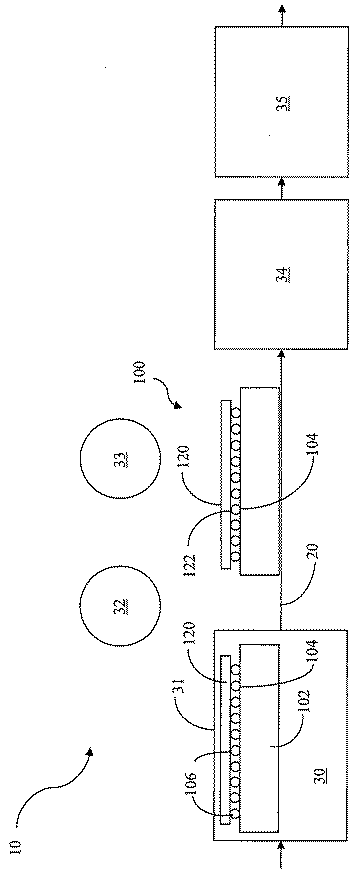
[0027]図1は、組立システム10の或る実施形態を描いている。組立システム10は、電子デバイス組立途上品100(図4及び図5)を、SMT部要素30、組立部要素40、そして少なくとも1つの塗被部要素50を通して輸送するコンベヤ20を含んでいる。コンベヤ20は組立ラインの一部を構成していてもよいし、或いはコンベヤ20は、自身が1つ又はそれ以上の電子デバイス組立途上品100を組立ライン(SMT部要素30及び/又は組立部要素40を含んでいるものとされる)からオフラインの塗被部要素50(及び、随意的には組立システム10のオフラインの他部構成要素)へ運び去り、そしてまた組立ラインへ戻すのを可能にする諸要素を含んでいてもよい。
FIG. 1 depicts an embodiment of an
[0028]コンベヤ20は、複数の電子デバイス組立途上品100を組立システム10のそれぞれの要素(例えば、SMT部要素30、組立部要素40、それぞれの塗被部要素50など)の各種構成要素へ搬入したり当該各種構成要素から搬出したりするための構成要素であって当技術で知られている多数の構成要素を含んでいてもよい。図2に描かれている様に、1つ又はそれ以上の要素(例えば、(単数又は複数の)塗被部要素50など)が、それぞれの電子デバイス組立途上品100が組立システム10を通って定常的に進んでゆくのを阻んでいる実施形態では、コンベヤ20は、制御装置24と、スループットを管理するように構成されている複数の構成要素と、を含むものとなろう。例えば、コンベヤ20は、複数の電子デバイス組立途上品100を、それらが定常スループットを阻害するそれぞれの要素又は構成要素(例えば、描かれている塗被部要素50など)へ導入されるより前に回収するように構成されている回収部構成要素26、そしてまた同様に複数の電子デバイス組立途上品100を、定常スループットを阻害するそれぞれの要素又は構成要素から受け取る給送部構成要素28を含むことができる。様々な実施形態では、電子デバイス製作途上品100が所望の速度でそれぞれの要素(及びその対応する構成要素)を通って輸送されるように、組立システム10のコンベヤ20の構成要素を同期させている。或る特定の実施形態では、その様な同期化は、制御装置24に実行させてコンベヤ20の各種構成要素の作動を制御させるプログラミングを介して遂行されている。
[0028]
[0029]図3に示されている様に、幾つかの実施形態では、塗被部要素50は、組立システム10のSMT部要素30から上流に置かれている。その様な実施形態では、塗被部要素50は、耐水性被覆110(例えば、パリレンCなど)をそれぞれの回路盤102及び/又はそれぞれのSMTデバイス120に塗工するように構成されている。関連付けられている装置52(例えば、マスキング及びエッチイングデバイスなど)は、回路盤102の接点要素104(例えば、接点パッド、端子など)(図4)又はSMTデバイス120の接点要素122(例えば、リード、導電パッド、端子など)(図4)をそれぞれ耐水性被覆110から露出するように構成されている。
As shown in FIG. 3, in some embodiments, the
[0030]次に図4を参照して、SMT部要素30では、パッケージ化されていない半導体デバイス及び/又はパッケージ化されている半導体デバイスの様なSMTデバイス120が、回路盤102に電気的に結合され且つ物理的に固着される。図4は、はんだがSMTデバイス120を回路盤102に(又はSMTデバイス120側のパッド、リード、又は他の端子を回路盤102の相手方パッド、リード、又は他の端子に)に電気的に結合している組立品を描いているが、他の型式の介在導電要素(例えば、リードなど)を使用することもできる。幾つかの実施形態では、SMT部要素30は、自動化されており、よって、それぞれのSMTデバイス20を、回路盤102の適切な場所に、正しく配置させ、電気的に結合させ、且つ物理的に固着させられる装置を含んでいる。
[0030] Referring now to FIG. 4, in the
[0031]SMT部要素30は、導電性材料(例えば、アルミニウム、金、はんだなど)又は他の介在導電要素106を回路盤102の様々な接点要素104に付ける導体塗工部構成要素31を含んでいてもよい。接点要素104には多種多様な型式の介在導電要素106の何れが固着されていても又は形成されていてもよく、その様な導電要素には、限定するわけではないが、はんだボールや、電気伝導性材料である例えば金属、合金、導電性エポキシなどから形成されているカラム、ピラー、リード(例えば、J字形リード、ガルウイング形リードなど)又は他の構造体や、個別の電気的に絶縁されている導電要素を厚さ方向に延ばした誘電体基板を含んでいる所謂「z軸」導電膜などが含まれる。介在導電要素106がはんだから形成されている実施形態では、導体塗工部構成要素31は、(はんだとフラックスを含んでいる)はんだペーストを接点要素104に選択的に塗工するための装置(例えば、スクリーン印刷装置、ジェット印刷デバイス、など)を備えることができるであろう。
[0031] The
[0032]ピックアンドプレイス部構成要素32が、それぞれの回路盤102を、導体塗工部構成要素31からコンベヤ20上の適切な場所へ輸送している。コンベヤ20がそれぞれの回路盤102を輸送してゆく際、別のピックアンドプレイス部構成要素33が1つ又はそれ以上のSMTデバイス120を回路盤102と一体に組み立てている。それぞれのSMTデバイス120と回路盤102との組立中、SMTデバイス120の接点要素122は回路盤102の相手方接点要素104と整列させられ、そうしてSMTデバイス120が回路盤102に固着される。後に介在導電要素106を形成させるべくはんだペーストを回路盤102の接点要素104に塗工してしまっている実施形態では、それぞれのSMTデバイス120を回路盤102と一体に組み立ててゆく際、SMTデバイス120の接点要素122を回路盤102の相手方接点要素104から突き出ている介在導電要素106(又はその先駆物質である例えば或る量のはんだペーストなど)へ接触させる。
[0032] Pick and
[0033]回路盤102とその(単数又は複数の)SMTデバイス120が組み立てられてしまうと、コンベヤ20は、得られた電子デバイス組立途上品100を結合部構成要素34へ輸送することができる。介在導電要素106がはんだから形成されることになっている実施形態では、結合部構成要素34は、リフローオーブンの様なはんだリフロー装置を備えることができるであろう。当然ながら、組立システム10のSMT部要素30には、1つ又はそれ以上のSMTデバイス120をそれぞれの回路盤102に電気的に結合するのに使用される介在導電要素106にとって適切とされる結合部構部要素34の他の実施形態が含まれていてもよい。
[0033] Once the
[0034]SMT部要素30は、随意的に、1つ又はそれ以上の清浄部構成要素35を含んでいてもよい。清浄部構成要素35が含まれている場合、清浄部構成要素35は、耐水性被覆の電子デバイス組立途上品100への接着を促すことになろう。より具体的には、清浄部構成要素35は、耐水性被覆の電子デバイス組立途上品表面への接着を妨げかねない残留フラックス又は他の汚染物質を電子デバイス組立途上品100の表面から少なくとも部分的に除去することができるであろう。限定するわけではないが、SMT部要素30の清浄部構成要素35は、脱気装置、洗浄(及び随意に乾燥)装置、汚染物質の有害効果を小さくするための他の装置、又は上記の何れかの組合せを含んでいてもよい。脱気装置は、耐水性被覆の接着を妨げかねない残留フラックスの揮発性化合物の電子デバイス組立途上品100からの除去を促すことができるであろう。洗浄装置は、実質的に、残留フラックスを丸ごと電子デバイス組立途上品100から除去することができるであろう。他の装置は、各種技法(例えば、脱脂、酸化、気化、壊変、物的移動など)により、汚染物質の有害効果を減少させることができるであろう。
[0034] The
[0035]SMTデバイス120と回路盤102との組立に先行して耐水性被覆110が回路盤102及び/又はSMTデバイス120に塗工されてしまっている実施形態(図3)では、残留フラックス又は他の汚染物質が電子デバイス組立途上品100上に滞留しているか否かに関わらず、清浄部構成要素35をSMT部要素30の一部として含める理由は全くなくなる。加えて、耐水性被覆110が回路盤102及び/又はSMTデバイス120に、それらの組立に先立って、塗工される速度は、同じ耐水性材料(例えば、パリレンCなど)が以降に回路盤102とSMTデバイス120の間に導入される速度より速くてもよく、同じ耐水性材料を回路盤102とSMTデバイス120の間への導入した場合よりも高い信頼度の耐水性を提供することができるであろう。
[0035] In an embodiment (FIG. 3) where the water
[0036]その様な実施形態では、他の構成要素が電子デバイス組立途上品100と一体に組み立てられる前に、耐水性被覆110の少なくとも一部分がSMTデバイス120と回路盤102の間に在ってもよい。幾つかの実施形態では、フラックス及び/又は他の汚染物質が、耐水性被覆110の露出している面上に存在しているかもしれない。
[0036] In such embodiments, at least a portion of the water
[0037]ひとたび、(単数又は複数の)SMTデバイス120が回路盤102と一体に組み立てられ電気的に結合されたら、電子デバイス組立途上品100の更なる加工が行われることになる。図5に示されている様に、コンベヤ20は、電子デバイス組立途上品100(図4と図5)を、何らかの(更なる)塗被が行われる前に、組立システム100の組立部要素40へ輸送している。他の実施形態では、コンベヤ20は、電子デバイス組立途上品100を、SMT部要素30から、直接、塗被部要素50へ輸送している。
[0037] Once the SMT device (s) 120 is assembled and electrically coupled to the
[0038]組立部要素40についてはその様々な代表的な実施形態を図6に示しているが、当該組立部要素40では、各種構成要素(即ち、電子デバイスの他の構成要素の全て)が回路盤102と一体に組み立てられて電子デバイス完成品100’が組み上がる。組立部要素40によって回路盤102に加えられる構成要素には、電子部品107、ユーザーインターフェース機構108、及びハウジング要素109が含まれる。組立部要素40は、自動式構成要素、手作業式構成要素(即ち、人が諸構成要素を回路盤に組み付けたり電気的に結合したりする)、又は自動式構成要素と手作業式構成要素の組合せを含んでいてもよい。
[0038] Although various representative embodiments of the
[0039]電子部品107には、裸の半導体デバイス又はパッケージ化された半導体デバイスはもとより、標準的なSTMデバイスとは異なった形状をしていて、そのため時に「不正規」又は「異形」電子的構成要素と呼称されることもある部品や、SMT部要素30の各種構成要素によって発生する温度又は使用される温度に感受性のある部品も含まれる。その様な電子部品107の非限定的な例には、モジュール、補助盤、アンテナ、入力デバイス(例えば、マイクロホン、カメラ、タッチセンシティブ要素など)、出力デバイス(例えば、スピーカー、ディスプレイスクリーン、ヘッドホンジャックなど)、ポート(例えば、バッテリ充電用、通信用など)、フラッシュ(照明)、近接センサー、サイレントモード用構成要素、更には電子デバイス(例えば、抵抗子、コンデンサ、誘導子、ダイオードなど)、並びに他の構成要素が含まれる。
[0039] The electronic component 107 is shaped differently than a standard STM device, as well as a bare semiconductor device or a packaged semiconductor device, and thus sometimes an "irregular" or "anomalous" electronic Components that are sometimes referred to as components, and components that are sensitive to temperatures generated or used by various components of the
[0040]何れの電子部品107についても、それを電子デバイス組立途上品100のもう一方の構成要素へ(例えば、電子デバイス組立途上品100の回路盤102や他の電子部品107などへ)電気的に結合するのに、各種の既知の技法を使用することができるであろう。例えば、1つ又はそれ以上のはんだ付けステーション41を使用して、電子的構成要素を回路盤102にはんだ付けするようにしてもよい。はんだ付けステーション41は、はんだ付け機器を手で操作する人を収容するように構成されていてもよい。代わりに、又は追加的に、はんだ付けステーションは自動化されていてもよい(例えば、レーザービーム、集束赤外線ビーム、局在対流機器などを採用)。
[0040] Any electronic component 107 is electrically connected to the other component of the electronic device assembly 100 (eg, to the
[0041]別の例として、電子部品は、1つ又はそれ以上のプラグインステーション42で、回路盤102の中へ(又は、少なくとも、回路盤102と関係付けられている差込口の中へ)差し込まれてもよい。プラグインステーション42は、電子部品を電子デバイス組立途上品100へ手作業で(例えば、曲げコネクタなどを用いて)接続する人を収容するものであってもよいし、プラグインステーション42は、電子部品を電子デバイス組立途上品100へ結合するための自動化された機器を備えていてもよいし、或いは組立システム10は手作業式プラグインステーション42と自動式プラグインステーション42の組合せを含んでいてもよい。
[0041] As another example, an electronic component may be inserted into the circuit board 102 (or at least into an outlet associated with the circuit board 102) at one or more plug-in stations 42. ) May be plugged in. The plug-in
[0042]当然ながら、組立部要素40は、電子部品を電子デバイス組立途上品100へ電気的に結合するのに適した、当技術で知られている他の電気接続部構成要素43、又は異なった型式の電気接続部構成要素(例えば、はんだ付けステーション41、プラグインステーション42、及び/又は他の電気関連構成要素43)の組合せ、を含んでいてもよい。
[0042] Of course, the
[0043]ユーザーインターフェース構成要素108である、例えば、ボタン、ノブ、スイッチ、キーボード、ディスプレイカバーなどに加え、バッテリ、ケーブル、ハウジング構成要素109、及び電子デバイス完成品100’の他の構成要素は、組立システム10の組立部要素40の1つ又はそれ以上のケース組立部構成要素44において電子デバイス組立途上品100と一体に組み立てられる。それぞれのケース組立部構成要素44は、手作業式要素(例えば、人が諸構成要素をデバイス製作途上品100と一体に組み立てる1つ又はそれ以上のステーションなど)、自動式要素、又は手作業式要素と自動式要素の組合せを含んでいてもよい。
[0043] In addition to the user interface components 108, such as buttons, knobs, switches, keyboards, display covers, etc., the battery, cable, housing component 109, and other components of the electronic device finished product 100 'include: One or more
[0044]図6は、塗被部要素50を組立部要素40に対して配置させることのできる多数の実施可能な設置場所を示している。塗被部要素50の当該設置場所は、耐水性被覆を、電子デバイス完成品100’の構成要素(例えば、電子部品107、ユーザーインターフェース構成要素108、ハウジング構成要素109など)に、それらが他の構成要素又は電子デバイス組立途上品100と一体に組み立てられるに先立って、塗工できるようにしている。塗被部要素50は、組立部要素40内の、耐水性被覆が電子デバイス組立途上品100の必要不可欠な機構(例えば、内部構成要素など)全てに塗工されることを確保できる場所に配置させることができる。電子デバイス完成品100’の内部及び/又は外部の全体又は部分に被覆を提供する場合は、塗被部要素50を組立部要素40の他の構成要素から下流に配置させて使用することができるであろう。
[0044] FIG. 6 shows a number of possible installation locations where the
[0045]2つ又はそれ以上の塗被部要素50を組立部要素40に含めれば、耐水性被覆の、電子デバイス組立途上品100の必要不可欠な機構への塗工、そしてひいては電子デバイス完成品100’の内部の塗工が更に最適化されることになろう。幾つかの実施形態では、塗被部要素50は、耐水性被覆を、電子デバイス組立途上品100の露出している表面に、又は電子デバイス組立途上品100と一体に組み立てられることになっている構成要素であって最終的には電子デバイス完成品100’の内部の内に置かれることになる、即ち、電子デバイス完成品100’内に閉じ込められることになる構成要素に、塗工するように配置させることができる。
[0045] If two or
[0046]塗被部要素50は、塗被装置の様々な実施形態の何れを又は何れの組合せを備えていてもよい。或る特定の実施形態では、組立システム10の塗被部要素50は、反応性モノマーを形成し、当該モノマーを次いで耐水性又は防水性にしようとする1つ又はそれ以上の表面に堆積させてポリマーを形成させる装置を備えている。特定の実施形態では、塗被部要素は、耐水性又は防水性にさせようとする1つ又はそれ以上の表面上へ、ポリ(p‐キシリレン)(即ち、パリレン)を、その非置換体及び/又は置換体を含め、堆積させるように構成されている。この方式で機能する塗被部要素の例が、米国特許出願第12/104,080号、同第12/104,152号、及び同第12/988,103号に記載されており、前記特許出願それぞれの開示全体をこれにより参考文献としてここに援用する。また米国特許出願第12/446,999号、同第12/669,074号、及び同第12/740,119号は、それらどれもの開示全体をこれにより参考文献としてここに援用するものであり、組立システム10の塗被部要素50が耐水性被覆を形成するために採用することのできる機器及び/又はプロセスの実施形態を開示している。組立システム10の塗被部要素50として採用することのできる装置の様々な実施形態には、限定するわけではないが、分子拡散機器、化学気相堆積(CVD)機器、物理気相堆積(PVD)機器(例えば、蒸発堆積プロセスを採用しているデバイス(限定するわけではないが、e−ビーム蒸発、スパッタリング、レーザー焼灼、パルスレーザー堆積など))、及び物理的塗工装置(例えば、印刷機器、吹付機器、回転塗布機器、刷毛塗り機器など)が含まれる。当然ながら、組立システム10では塗被部要素50の他の実施形態を使用することもできる。
[0046] The
[0047]組立システム10の塗被部要素50により塗工することのできる材料には、熱可塑性材料、硬化性材料(例えば、放射線硬化性材料、二部構成材料、熱硬化性材料、室温硬化性材料など)が含められるが、決してそれらに限定されるものではない。幾つかの実施形態では、塗被部要素50は、所望の耐水性レベルを提供するのに十分な厚さを有する耐水膜を比較的短時間の内に塗工するように構成されている。様々な実施形態では、塗被部要素50は、少なくとも1ミクロンの最小厚さ又は平均厚さを有する膜(例えば、パリレン膜など)を、1時間未満で、約15分以下で、約5分以下で、又は約2分以下で堆積させるように構成されている。
[0047] Materials that can be applied by the
[0048]組立システム10全体としての観点では、所望の型式の被覆を異なった型式の機構に提供するため、複数の異なった塗被部要素50、更には異なった型式の塗被部要素50を設置することができるであろう。限定するわけではないが、1つの塗被部要素50が、耐水性被覆を電子デバイス組立途上品100の異なった構成要素の間(例えば、SMT構成要素104と回路盤102の間など)の小空間に提供するように構成されており、一方で、別の塗被部要素50が、塗被プロセス中に露出される表面に共形ブランケット耐水性被覆を提供するように構成されており、そしてまた別の塗被部要素50が、耐水性被覆を一部の特定の機構に選択的に塗工するようになっていてもよい。
[0048] In view of the
[0049]再び図1に戻って、組立システム10は、組立システム10の上記要素に加えて、追加の構成要素を含んでいてもよい。
[0050]幾つかの実施形態では、組立システム10は、1つ又はそれ以上のマスキング装置60を含んでいる。マスキング装置60は、耐水性被覆の塗工が所望されていない表面(例えば、間欠的な機械的接続が所望されている電気接点など)に耐水性被覆が塗工されるのを防止するように構成されている。マスキング装置60の幾つかの実施形態は、耐水性被覆を塗工しようとする構成要素と一体に組み立てられるように構成されている物理的マスキング要素を備えており、一方で、マスキング装置60の他の実施形態は、耐水性被覆を塗工しようとする構成要素上に選択的に除去できる仮のマスクを堆積させるように構成されている。当然ながら、1つ又はそれ以上のマスキング装置60を塗被部要素50から上流に含んでいる組立システム10は、更に、マスキングされその結果耐水性被覆を接着させなかった機構を露出するために1つ又はそれ以上のマスク除去部要素(図示せず)を塗被部要素50から下流に含むことになろう。
[0049] Returning again to FIG. 1, the
[0050] In some embodiments, the
[0051]組立システム10の幾つかの実施形態は、1つ又はそれ以上の表面処理部要素70を含んでいてもよい。表面処理部要素は、電子デバイス組立途上品100の表面を耐水性被覆塗工のために前処理するように構成されている。幾つかの実施形態では、表面処理部要素70は、電子デバイス組立途上品100の少なくとも一部分への耐水性被覆の接着を増進するように構成されている。表面処理部要素70は、電子デバイス組立途上品100の少なくとも一部分の表面を、耐水性被覆に少なくとも1つの所望の特性(例えば、所謂「蓮の葉」構造又は肌理の様な撥水性など)が付与されるやり方で改質するように構成されていてもよい。代わりに、又は追加的に、表面処理部要素70は、電子デバイス組立途上品100の表面を、当該電子デバイス組立途上品100の少なくとも諸部分に耐水性被覆が塗工された後に、清浄するなり又はそれ以外のやり方で処理するなりしてもよい。
[0051] Some embodiments of the
[0052]組立システム10は、塗被部要素50から下流に設置されている少なくとも1つの塗被検査部要素80を含んでいてもよい。それぞれの塗被検査部要素80は、耐水性被覆の存在、耐水性被覆の厚さ、耐水性被覆が在る表面、耐水性被覆の品質、又は塗被部要素により電子デバイス組立途上品100に塗工された耐水性被覆に関するその他の有用な情報、の分析ができるようになっている。塗被検査部要素80からの情報は、当該検査部要素80と関係付けられている塗被部要素50に対する、或いは組立システム10のその他の構成要素に対する、フィードバック制御を提供するのに使用することができるであろう。
[0052] The
[0053]幾つかの実施形態では、組立システム10は、材料除去部要素90を含んでいてもよい。材料除去部要素90は、材料を、耐水性被覆の1つ又はそれ以上の領域から選択的に除去するように構成されている。その様な材料除去は、何らかの適した手段により、材料が除去される電子デバイス組立途上品の下層の又は隣接する諸部分に有害な影響を及ぼさずに行われるものである。一例として、材料除去部要素90は、耐水性被覆の材料を、(例えば、正しく位置を定めたパルスレーザービーム又は連続レーザービームを用いて)焼灼するか、気化させるか、又は昇華させるように構成されていてもよい。別の例として、材料除去部要素90は、溶剤を(例えば、インクジェットプロセス、スクリーン印刷などにより)選択的に塗工して、電子デバイス組立途上品の耐水性被覆の材料を選択的に除去させるようにしてもよい。更に別の例では、材料除去部要素90は、耐水性被覆の1つ又はそれ以上の選択領域から材料を(例えば、切削、研磨などにより)機械的に除去するように構成されていてもよい。
[0053] In some embodiments, the
[0054]以上の説明には多数の詳細事項が含まれているが、それらは、本発明或いは付随の特許請求の範囲の何れについてもその範囲を限定するものではなく、本発明及び特許請求の範囲による範囲の内に入る幾つかの特定の実施形態に関する情報を提供しているにすぎないと解釈されるべきである。異なった実施形態による特徴を組み合わせて採用することもできるであろう。更には、本発明の実施形態で、本発明及び特許請求の範囲による範囲の内に属する他の実施形態を考案することもできるであろう。故に、本発明の範囲は、付随の特許請求の範囲及びそれらの法的等価物によってのみ示され、限定される。ここに開示されている本発明への追加、削除、及び変更で、特許請求の範囲の意味及び範囲の内に入るあらゆる追加、削除、及び変更は、特許請求の範囲によって包含されるものとする。 [0054] While the foregoing description includes numerous details, they are not intended to limit the scope of the invention or any of the appended claims. It should be construed as merely providing information regarding some specific embodiments that fall within the scope of the scope. A combination of features from different embodiments could also be employed. Furthermore, other embodiments within the scope of the present invention and claims may be devised with embodiments of the present invention. Accordingly, the scope of the invention is indicated and limited only by the appended claims and their legal equivalents. Any additions, deletions, and modifications to the invention disclosed herein that fall within the meaning and scope of the claims are intended to be embraced by the claims. .
10 組立システム
20 コンベヤ
24 制御装置
26 回収部構成要素
28 給送部構成要素
30 SMT部要素
31 導体塗工部構成要素
32、33 ピックアンドプレイス部構成要素
34 結合部構成要素
35 清浄部構成要素
40 組立部要素
41 はんだ付けステーション
42 プラグインステーション
43 電気接続部構成要素
44 ケース組立部構成要素
50 塗被部要素
52 関係付けられている機器
60 マスキング装置
70 表面処理部要素
80 塗被検査部要素
90 材料除去部要素
100 電子デバイス組立途上品
100’ 電子デバイス完成品
102 回路盤
104 回路盤の接点要素
106 介在導電要素
107 電子部品
108 ユーザーインターフェース機構
109 ハウジング要素
110 耐水性被覆
120 SMTデバイス
122 SMTデバイスの接点要素
DESCRIPTION OF
Claims (47)
少なくとも1つの表面実装技術(SMT)構成要素を回路盤と一体に組み立てて電子的半組立品を形成させるSMT部要素と、
電子部品、ユーザーインターフェース構成要素、及びハウジング構成要素を前記電子的半組立品と一体に組み立てる組立部要素と、
耐水性被覆を、前記電子的半組立品の電気接続を覆って塗工することを含め、当該電子的半組立品の少なくとも一部分に塗工する塗被部要素と、を備えているシステム。 In a system for assembling electronic devices,
An SMT component that assembles at least one surface mount technology (SMT) component together with a circuit board to form an electronic subassembly;
An assembly component for assembling electronic components, user interface components, and housing components together with the electronic subassembly;
A coating element for applying to at least a portion of the electronic subassembly including applying a water-resistant coating over the electrical connections of the electronic subassembly.
表面実装技術(SMT)電子デバイスを回路盤上に配置し、介在導電要素を前記SMT電子デバイスと前記回路盤の間に形成して当該SMT電子デバイスと当該回路盤の間に電気通信を確立させるSMT組立部要素と、
複数の電気接続を電子部品と前記回路盤の間に作成して前記電子部品と前記回路盤の間に電気通信を確立させる組立部要素と、
耐水性被覆を前記介在導電要素又は前記電気接続に塗工するように構成されている塗被部要素と、を備えている、組立ライン。 In the assembly line,
A surface mount technology (SMT) electronic device is placed on the circuit board and an intervening conductive element is formed between the SMT electronic device and the circuit board to establish electrical communication between the SMT electronic device and the circuit board. An SMT assembly element;
An assembly element that creates a plurality of electrical connections between an electronic component and the circuit board to establish electrical communication between the electronic component and the circuit board;
An assembly line comprising: a coating element configured to apply a water resistant coating to the intervening conductive element or the electrical connection.
耐水性被覆を電子デバイス組立途上品に塗工する段階と、
前記耐水性被覆を塗工する段階の後に、少なくとも1つの構成要素を前記電子デバイス組立途上品と一体に組み立てる段階と、を備えている方法。 In a method for imparting water resistance to an electronic device,
Applying a water-resistant coating to an electronic device assembly product;
Assembling at least one component integrally with the electronic device assembly after the step of applying the water resistant coating.
Applications Claiming Priority (2)
| Application Number | Priority Date | Filing Date | Title |
|---|---|---|---|
| US201261584918P | 2012-01-10 | 2012-01-10 | |
| US61/584,918 | 2012-01-10 |
Related Child Applications (1)
| Application Number | Title | Priority Date | Filing Date |
|---|---|---|---|
| JP2014216005A Division JP2015079963A (en) | 2012-01-10 | 2014-10-23 | System for assembling electronic device with internal water-resistant coating |
Publications (1)
| Publication Number | Publication Date |
|---|---|
| JP2013143563A true JP2013143563A (en) | 2013-07-22 |
Family
ID=48723092
Family Applications (3)
| Application Number | Title | Priority Date | Filing Date |
|---|---|---|---|
| JP2012096417A Pending JP2013143563A (en) | 2012-01-10 | 2012-04-20 | Systems for assembling electronic devices with internal moisture-resistant coatings |
| JP2014216005A Pending JP2015079963A (en) | 2012-01-10 | 2014-10-23 | System for assembling electronic device with internal water-resistant coating |
| JP2016037249A Pending JP2016129245A (en) | 2012-01-10 | 2016-02-29 | System for assembling an electronic device with an internal water-resistant coating |
Family Applications After (2)
| Application Number | Title | Priority Date | Filing Date |
|---|---|---|---|
| JP2014216005A Pending JP2015079963A (en) | 2012-01-10 | 2014-10-23 | System for assembling electronic device with internal water-resistant coating |
| JP2016037249A Pending JP2016129245A (en) | 2012-01-10 | 2016-02-29 | System for assembling an electronic device with an internal water-resistant coating |
Country Status (8)
| Country | Link |
|---|---|
| US (2) | US9426936B2 (en) |
| EP (1) | EP2803084A4 (en) |
| JP (3) | JP2013143563A (en) |
| KR (2) | KR20130082050A (en) |
| CN (2) | CN104582301A (en) |
| AU (1) | AU2013208184B2 (en) |
| TW (2) | TWI452951B (en) |
| WO (1) | WO2013106334A1 (en) |
Families Citing this family (14)
| Publication number | Priority date | Publication date | Assignee | Title |
|---|---|---|---|---|
| US9146207B2 (en) | 2012-01-10 | 2015-09-29 | Hzo, Inc. | Methods, apparatuses and systems for sensing exposure of electronic devices to moisture |
| EP2803083A4 (en) | 2012-01-10 | 2014-12-31 | Hzo Inc | MASKS FOR APPLYING PROTECTIVE COATINGS TO ELECTRONIC ASSEMBLIES, MASKED ELECTRONIC ASSEMBLIES, AND ASSOCIATED METHODS |
| WO2013106450A1 (en) | 2012-01-10 | 2013-07-18 | Hzo, Inc. | Precursor supplies, material processing systems with which precursor supplies are configured to be used and associated methods |
| AU2013208273B2 (en) | 2012-01-10 | 2015-11-26 | Hzo, Inc. | Methods, apparatuses and systems for monitoring for exposure of electronic devices to moisture and reacting to exposure of electronic devices to moisture |
| CN104364020A (en) | 2012-06-18 | 2015-02-18 | Hzo股份有限公司 | Systems and methods for applying protective coatings to internal surfaces of fully assembled electronic devices |
| US9894776B2 (en) | 2013-01-08 | 2018-02-13 | Hzo, Inc. | System for refurbishing or remanufacturing an electronic device |
| JP2016509533A (en) | 2013-01-08 | 2016-03-31 | エイチズィーオー・インコーポレーテッド | Masking substrates for protective coatings |
| EP2944011A4 (en) | 2013-01-08 | 2016-01-27 | Hzo Inc | APPARATUSES, SYSTEMS AND METHODS FOR REDUCING POWER ON PORTS OF ELECTRONIC DEVICES |
| US10449568B2 (en) | 2013-01-08 | 2019-10-22 | Hzo, Inc. | Masking substrates for application of protective coatings |
| WO2014110159A1 (en) | 2013-01-08 | 2014-07-17 | Hzo, Inc. | Apparatuses, systems, and methods for detecting and reacting to exposure of an electronic device to moisture |
| WO2016033248A1 (en) * | 2014-08-26 | 2016-03-03 | Hzo, Inc. | Use of combined masking techniques and/or combined material removal techniques to protectively coat electronic devices |
| CN105337093B (en) | 2015-08-19 | 2018-11-09 | 富士康(昆山)电脑接插件有限公司 | Electric connector |
| CN110005673B (en) * | 2019-04-16 | 2023-12-01 | 广东得胜电子有限公司 | Assembling production line for upper pad disc, tuning paper and loudspeaker of earphone |
| CN114173487A (en) * | 2020-09-10 | 2022-03-11 | 耐世特汽车系统(苏州)有限公司 | Circuit board protection method and circuit board assembly |
Citations (2)
| Publication number | Priority date | Publication date | Assignee | Title |
|---|---|---|---|---|
| JPH1093228A (en) * | 1996-09-18 | 1998-04-10 | Sumitomo Wiring Syst Ltd | Printed circuit board and its manufacture |
| JP2002514004A (en) * | 1998-05-01 | 2002-05-14 | セシュー ビー デス | Oxide / organic polymer multilayer thin films deposited by chemical vapor deposition |
Family Cites Families (53)
| Publication number | Priority date | Publication date | Assignee | Title |
|---|---|---|---|---|
| US4335698A (en) | 1979-11-13 | 1982-06-22 | Max-Mi Corporation | Vaporization chamber |
| JPS63194393A (en) * | 1987-02-07 | 1988-08-11 | 株式会社電子技研 | Method and apparatus for forming film of electronic circuit substrate |
| US5271953A (en) | 1991-02-25 | 1993-12-21 | Delco Electronics Corporation | System for performing work on workpieces |
| US5387444A (en) | 1992-02-27 | 1995-02-07 | Dymax Corporation | Ultrasonic method for coating workpieces, preferably using two-part compositions |
| AU4652993A (en) | 1992-06-26 | 1994-01-24 | Materials Research Corporation | Transport system for wafer processing line |
| JPH06102374A (en) | 1992-09-18 | 1994-04-15 | Fujitsu Ltd | Watch type equipment |
| US5429682A (en) | 1993-08-19 | 1995-07-04 | Advanced Robotics Technologies | Automated three-dimensional precision coatings application apparatus |
| JPH07211178A (en) | 1994-01-21 | 1995-08-11 | Yokogawa Electric Corp | Waterproof system panel |
| US5536282A (en) | 1994-11-08 | 1996-07-16 | Cincinnati Milacron Inc. | Method for producing an improved vitreous bonded abrasive article and the article produced thereby |
| US5536317A (en) | 1995-10-27 | 1996-07-16 | Specialty Coating Systems, Inc. | Parylene deposition apparatus including a quartz crystal thickness/rate controller |
| JP3288925B2 (en) | 1996-05-10 | 2002-06-04 | 株式会社小糸製作所 | Electronic device and method of manufacturing the same |
| US6127038A (en) | 1997-12-11 | 2000-10-03 | American Meter Company | Printed circuit board coating and method |
| EP1030349B2 (en) | 1999-01-07 | 2013-12-11 | Kulicke & Soffa Die Bonding GmbH | Method and apparatus for treating electronic components mounted on a substrate, in particular semiconductor chips |
| JP2000211993A (en) | 1999-01-22 | 2000-08-02 | Mitsubishi Electric Corp | Semiconductor wafer manufacturing method, semiconductor manufacturing apparatus, and semiconductor device |
| DE19913628A1 (en) | 1999-03-25 | 2000-10-05 | Siemens Ag | Plant for the production of semiconductor products |
| DE10023456A1 (en) * | 1999-07-29 | 2001-02-01 | Creavis Tech & Innovation Gmbh | Mesotubes and nanotubes |
| JP2001068831A (en) | 1999-08-27 | 2001-03-16 | Minami Kk | Method for coating component-mounted substrate with anticorrosive material |
| US7239227B1 (en) | 1999-12-30 | 2007-07-03 | Upek, Inc. | Command interface using fingerprint sensor input system |
| SG90171A1 (en) | 2000-09-26 | 2002-07-23 | Inst Data Storage | Sputtering device |
| JP2002151834A (en) * | 2000-11-10 | 2002-05-24 | Fujitsu Ten Ltd | Dehumidifying method of substrate |
| US20020187350A1 (en) | 2001-01-29 | 2002-12-12 | Honeywell International Inc. | Robust highly reflective optical construction |
| US6788987B2 (en) * | 2001-03-07 | 2004-09-07 | Siemens Electronic Assembly Systems, Inc. | System and processes for performing quick changeovers on assembly lines |
| US6559411B2 (en) | 2001-08-10 | 2003-05-06 | First Solar, Llc | Method and apparatus for laser scribing glass sheet substrate coatings |
| US7003477B2 (en) * | 2002-03-01 | 2006-02-21 | Phillip Zarrow | Certification method for manufacturing process |
| US6932871B2 (en) | 2002-04-16 | 2005-08-23 | Applied Materials, Inc. | Multi-station deposition apparatus and method |
| US7008483B2 (en) * | 2002-04-19 | 2006-03-07 | Hewlett-Packard Development Company, L.P. | Curing printed circuit board coatings |
| TWI268813B (en) * | 2002-04-24 | 2006-12-21 | Sipix Imaging Inc | Process for forming a patterned thin film conductive structure on a substrate |
| US9725805B2 (en) | 2003-06-27 | 2017-08-08 | Spts Technologies Limited | Apparatus and method for controlled application of reactive vapors to produce thin films and coatings |
| US7673970B2 (en) | 2004-06-30 | 2010-03-09 | Lexmark International, Inc. | Flexible circuit corrosion protection |
| CA2622023A1 (en) | 2005-10-14 | 2007-04-26 | Advanced Plastics Technologies Luxembourg S.A. | Methods of forming multilayer articles by surface treatment applications |
| US20070108161A1 (en) | 2005-11-17 | 2007-05-17 | Applied Materials, Inc. | Chamber components with polymer coatings and methods of manufacture |
| JP4830523B2 (en) | 2006-02-08 | 2011-12-07 | 東京エレクトロン株式会社 | Coating, developing apparatus, coating, developing method and computer program for carrying out the method. |
| GB0610432D0 (en) | 2006-05-26 | 2006-07-05 | B G Res Ltd | Performance issues in use of vessels for biological applications |
| GB0621520D0 (en) | 2006-10-28 | 2006-12-06 | P2I Ltd | Novel products |
| ES2397719T3 (en) | 2007-07-17 | 2013-03-11 | P2I Ltd | Procedure for the liquid waterproofing of an article of footwear by plasma graft polymerization |
| US20090263581A1 (en) | 2008-04-16 | 2009-10-22 | Northeast Maritime Institute, Inc. | Method and apparatus to coat objects with parylene and boron nitride |
| US20090263641A1 (en) | 2008-04-16 | 2009-10-22 | Northeast Maritime Institute, Inc. | Method and apparatus to coat objects with parylene |
| GB0721202D0 (en) | 2007-10-30 | 2007-12-05 | P2I Ltd | Novel method |
| CN105400269A (en) | 2008-04-16 | 2016-03-16 | Hzo股份有限公司 | Metal and electronic device coating process for marine use and other environments |
| SG10201701218UA (en) * | 2008-08-18 | 2017-03-30 | Semblant Ltd | Halo-hydrocarbon polymer coating |
| US8697189B2 (en) | 2008-10-21 | 2014-04-15 | Intevac, Inc. | Method and apparatus for precision surface modification in nano-imprint lithography |
| DE102008057154B4 (en) * | 2008-11-13 | 2012-06-21 | Bühler Motor GmbH | Centrifugal pump with a brushless DC motor |
| AR074873A1 (en) | 2008-12-22 | 2011-02-16 | Columbia Sportswear Na Inc | OUTDOOR ZIPPER ZIPPER CLOSURES |
| WO2010078264A2 (en) | 2008-12-31 | 2010-07-08 | Archers Inc. | Methods and systems of transferring, docking and processing substrates |
| US20100162954A1 (en) | 2008-12-31 | 2010-07-01 | Lawrence Chung-Lai Lei | Integrated facility and process chamber for substrate processing |
| US8300298B2 (en) | 2010-04-30 | 2012-10-30 | Soladigm, Inc. | Electrochromic devices |
| US8039289B2 (en) | 2009-04-16 | 2011-10-18 | Tp Solar, Inc. | Diffusion furnaces employing ultra low mass transport systems and methods of wafer rapid diffusion processing |
| JP2011050835A (en) * | 2009-09-01 | 2011-03-17 | Rexxam Co Ltd | Substrate coating apparatus and program |
| US20110143021A1 (en) * | 2009-12-15 | 2011-06-16 | Rockwell Automation Technologies, Inc. | Conformal coating system and method |
| BE1019159A5 (en) | 2010-01-22 | 2012-04-03 | Europlasma Nv | METHOD FOR DEPOSITING A EQUIVALENT NANOCOATING BY A LOW-PRESSURE PLASMA PROCESS |
| CN101959371A (en) * | 2010-05-27 | 2011-01-26 | 世达普(苏州)通信设备有限公司 | Manufacture method for ensuing integrated manufacture structure and dimension of printed circuit board |
| US8797756B2 (en) * | 2010-09-21 | 2014-08-05 | Biotronik Se & Co. Kg | Integrated overmolded interconnect tab for surface-mounted circuits |
| US8852693B2 (en) | 2011-05-19 | 2014-10-07 | Liquipel Ip Llc | Coated electronic devices and associated methods |
-
2012
- 2012-04-20 JP JP2012096417A patent/JP2013143563A/en active Pending
- 2012-05-17 TW TW101117536A patent/TWI452951B/en active
- 2012-05-17 TW TW103126177A patent/TWI549581B/en active
- 2012-05-21 CN CN201410743157.3A patent/CN104582301A/en active Pending
- 2012-05-21 CN CN201210158907.1A patent/CN103200787B/en not_active Expired - Fee Related
- 2012-06-18 KR KR1020120064868A patent/KR20130082050A/en not_active Ceased
-
2013
- 2013-01-08 EP EP13735656.4A patent/EP2803084A4/en not_active Ceased
- 2013-01-08 WO PCT/US2013/020683 patent/WO2013106334A1/en not_active Ceased
- 2013-01-08 AU AU2013208184A patent/AU2013208184B2/en not_active Ceased
- 2013-01-08 US US13/736,753 patent/US9426936B2/en active Active
-
2014
- 2014-10-23 JP JP2014216005A patent/JP2015079963A/en active Pending
- 2014-12-10 KR KR1020140177299A patent/KR20140147074A/en not_active Ceased
-
2016
- 2016-02-29 JP JP2016037249A patent/JP2016129245A/en active Pending
- 2016-07-08 US US15/205,696 patent/US10070569B2/en active Active
Patent Citations (2)
| Publication number | Priority date | Publication date | Assignee | Title |
|---|---|---|---|---|
| JPH1093228A (en) * | 1996-09-18 | 1998-04-10 | Sumitomo Wiring Syst Ltd | Printed circuit board and its manufacture |
| JP2002514004A (en) * | 1998-05-01 | 2002-05-14 | セシュー ビー デス | Oxide / organic polymer multilayer thin films deposited by chemical vapor deposition |
Also Published As
| Publication number | Publication date |
|---|---|
| US20160324044A1 (en) | 2016-11-03 |
| AU2013208184A1 (en) | 2014-03-20 |
| EP2803084A1 (en) | 2014-11-19 |
| JP2016129245A (en) | 2016-07-14 |
| CN104582301A (en) | 2015-04-29 |
| EP2803084A4 (en) | 2015-03-04 |
| AU2013208184B2 (en) | 2014-08-28 |
| JP2015079963A (en) | 2015-04-23 |
| TW201330740A (en) | 2013-07-16 |
| US10070569B2 (en) | 2018-09-04 |
| CN103200787A (en) | 2013-07-10 |
| WO2013106334A1 (en) | 2013-07-18 |
| TWI452951B (en) | 2014-09-11 |
| CN103200787B (en) | 2017-05-10 |
| TWI549581B (en) | 2016-09-11 |
| US9426936B2 (en) | 2016-08-23 |
| TW201444436A (en) | 2014-11-16 |
| US20130174410A1 (en) | 2013-07-11 |
| KR20140147074A (en) | 2014-12-29 |
| KR20130082050A (en) | 2013-07-18 |
Similar Documents
| Publication | Publication Date | Title |
|---|---|---|
| JP2016129245A (en) | System for assembling an electronic device with an internal water-resistant coating | |
| US20200208258A1 (en) | Apparatuses, systems and methods for protecting electronic device assemblies | |
| CN104718258B (en) | surface coating | |
| US20110094889A1 (en) | Method for fabricating highly conductive fine patterns using self-patterned conductors and plating | |
| JP2013143564A (en) | Electronic device with inner waterproof coating | |
| JP2013527973A (en) | Plasma polymer coating | |
| KR102770638B1 (en) | Laminate for printed wiring board and printed wiring board using the same | |
| WO2015192146A1 (en) | Impermeable protective coatings through which electrical connections may be established and electronic devices including the impermeable protective coatings | |
| KR20150052827A (en) | Apparatuses, systems and methods for protecting electronic device assemblies | |
| CN101286490A (en) | Substrate surface treatment structure and manufacturing method thereof | |
| EP2862428A2 (en) | Apparatuses, systems and methods for protecting electronic device assemblies | |
| HK1182885A (en) | Systems for assembling electronic devices with internal water-resistant coatings | |
| US11477894B2 (en) | Method for formation of patterned solder mask | |
| JP5661775B2 (en) | Ceramic component manufacturing method, ceramic component and component assembly | |
| JP2017510708A (en) | Processing module for horizontal wet chemical processing equipment for large substrates | |
| JP2007053039A (en) | Electrical connector joint structure and flexible wiring board used therefor | |
| RU2329620C1 (en) | Method of printed circuit boards manufacturing | |
| US20200205295A1 (en) | System, Apparatus and Method for Utilizing Surface Mount Technology on Metal Substrates | |
| CN119676971A (en) | Flexible circuit board based on inkjet and PEVCD and its manufacturing method | |
| JP2015207678A (en) | Wiring board manufacturing method | |
| JP2010129943A (en) | Method of manufacturing printed circuit board |
Legal Events
| Date | Code | Title | Description |
|---|---|---|---|
| A977 | Report on retrieval |
Free format text: JAPANESE INTERMEDIATE CODE: A971007 Effective date: 20131127 |
|
| A131 | Notification of reasons for refusal |
Free format text: JAPANESE INTERMEDIATE CODE: A131 Effective date: 20131202 |
|
| A601 | Written request for extension of time |
Free format text: JAPANESE INTERMEDIATE CODE: A601 Effective date: 20140225 |
|
| A602 | Written permission of extension of time |
Free format text: JAPANESE INTERMEDIATE CODE: A602 Effective date: 20140228 |
|
| A601 | Written request for extension of time |
Free format text: JAPANESE INTERMEDIATE CODE: A601 Effective date: 20140402 |
|
| A602 | Written permission of extension of time |
Free format text: JAPANESE INTERMEDIATE CODE: A602 Effective date: 20140407 |
|
| A601 | Written request for extension of time |
Free format text: JAPANESE INTERMEDIATE CODE: A601 Effective date: 20140501 |
|
| A602 | Written permission of extension of time |
Free format text: JAPANESE INTERMEDIATE CODE: A602 Effective date: 20140508 |
|
| A521 | Written amendment |
Free format text: JAPANESE INTERMEDIATE CODE: A523 Effective date: 20140515 |
|
| A02 | Decision of refusal |
Free format text: JAPANESE INTERMEDIATE CODE: A02 Effective date: 20140623 |