JP2013104820A - Power consumption measurement device and power consumption measurement system - Google Patents
Power consumption measurement device and power consumption measurement system Download PDFInfo
- Publication number
- JP2013104820A JP2013104820A JP2011249962A JP2011249962A JP2013104820A JP 2013104820 A JP2013104820 A JP 2013104820A JP 2011249962 A JP2011249962 A JP 2011249962A JP 2011249962 A JP2011249962 A JP 2011249962A JP 2013104820 A JP2013104820 A JP 2013104820A
- Authority
- JP
- Japan
- Prior art keywords
- current
- power consumption
- measuring
- conductor
- outlet
- Prior art date
- Legal status (The legal status is an assumption and is not a legal conclusion. Google has not performed a legal analysis and makes no representation as to the accuracy of the status listed.)
- Pending
Links
Images


Landscapes
- Measuring Instrument Details And Bridges, And Automatic Balancing Devices (AREA)
Abstract
Description
本発明は、電気機器の消費電力を測定する消費電力測定装置及び消費電力測定システムに関する。 The present invention relates to a power consumption measuring device and a power consumption measuring system for measuring the power consumption of an electrical device.
電気機器の消費電力を測定する技術としては、コンセントに接続されるプラグと、測定対象である電気機器と接続されるコンセントプラグと、プラグ及びコンセントを接続する電力線と、この電力線における電圧値及び電流値に基づいて電気機器の消費電力を演算する演算部とを備え、電気機器の消費電力に関する情報を外部機器に無線送信する電力計測システムが知られている(特許文献1参照)。 The technology for measuring the power consumption of electrical equipment includes a plug connected to an outlet, an outlet plug connected to the electrical equipment to be measured, a power line connecting the plug and the outlet, and a voltage value and current in the power line. There is known a power measurement system that includes a calculation unit that calculates power consumption of an electric device based on a value and wirelessly transmits information related to the power consumption of the electric device to an external device (see Patent Document 1).
上記特許文献1に記載の電力計測システムでは、電気機器の消費電力を演算し、パーソナルコンピュータ等の外部装置に無線送信する技術が開示されている。
The power measurement system described in
近年では、上述したようなシステムを用いて、電気機器の消費電力を高精度または確実に計測したいという要望がある。 In recent years, there has been a demand for measuring the power consumption of electrical equipment with high accuracy or reliability using the system as described above.
そこで、本発明は、電気機器の使用状態を高精度または確実に測定できる消費電力測定装置及び消費電力測定システムを提供する。 Therefore, the present invention provides a power consumption measuring device and a power consumption measuring system that can measure the usage state of an electrical device with high accuracy or reliability.
本発明の消費電力測定装置は、被測定対象となる電気機器が接続されるコンセントと、外部電源に接続されるプラグと、前記コンセント及びプラグの間を接続する導体と、前記導体に印加される電圧を測定する電圧測定手段と、前記導体を流れる電流を測定する電流測定手段と、前記電圧測定手段から得られる電圧値と前記電流測定手段から得られる電流値とに基づいて、前記電気機器の消費電力を求める電力取得手段とを備え、前記電流測定手段は、前記導体を流れる被測定電流の流れ方向を別の方向に変更する電流方向変更領域と、前記電流方向変更領域により電流方向が変更された被測定電流によって生じる磁気を検知する磁気検知素子と、前記磁気検出素子の出力から前記被測定電流の電流値を求める電流値取得手段とを有することを特徴とする。 The power consumption measuring apparatus of the present invention is applied to the outlet to which the electrical device to be measured is connected, the plug connected to the external power supply, the conductor connecting the outlet and the plug, and the conductor. Based on the voltage measuring means for measuring the voltage, the current measuring means for measuring the current flowing through the conductor, the voltage value obtained from the voltage measuring means and the current value obtained from the current measuring means, A power acquisition means for obtaining power consumption, wherein the current measuring means changes a current direction changing area in which the flow direction of the current to be measured flowing through the conductor is changed to another direction, and the current direction is changed by the current direction changing area. A magnetic sensing element that detects magnetism generated by the measured current, and a current value acquisition unit that obtains a current value of the measured current from an output of the magnetic detection element And features.
また、上記本発明は、前記コンセントの使用時刻又は使用時間を計る計時手段と、前記コンセントの使用時刻又は使用時間に対応する前記電気機器の消費電力情報を記憶する記憶手段とを備えることが好ましい。 In addition, the present invention preferably includes a time measuring unit that measures the use time or use time of the outlet, and a storage unit that stores power consumption information of the electric device corresponding to the use time or use time of the outlet. .
さらに、上記本発明に係る記憶手段は、不揮発性メモリであることが好ましい。 Further, the storage means according to the present invention is preferably a nonvolatile memory.
また、上記本発明は、前記電力取得手段により求めた前記電気機器の消費電力に基づく消費電力情報を外部端末に無線により送信する送信手段を更に備えることが好ましい。 Moreover, it is preferable that the present invention further includes a transmission unit that wirelessly transmits power consumption information based on the power consumption of the electrical device obtained by the power acquisition unit to an external terminal.
さらに、上記本発明に係る前記送信手段は、前記外部端末との接続が切断状態から接続状態に移行後に、前記外部端末に未送信の前記電気機器の消費電力情報を送信することが好ましい。 Furthermore, it is preferable that the transmission means according to the present invention transmits the power consumption information of the untransmitted electrical device to the external terminal after the connection with the external terminal shifts from a disconnected state to a connected state.
さらに、本発明の消費電力測定装置は、被測定対象となる電気機器が接続されるコンセントと、外部電源に接続されるプラグと、前記コンセント及びプラグの間を接続する導体と、前記導体に印加される電圧を測定する電圧測定手段と、前記導体を流れる電流を測定する電流測定手段と、前記電圧測定手段から得られる電圧値と前記電流測定手段から得られる電流値とに基づいて、前記電気機器の消費電力を求める電力取得手段と、前記コンセントの使用時刻又は使用時間を計る計時手段と、前記コンセントの使用時刻又は使用時間に対応した前記電気機器の消費電力に基づく消費電力情報を記憶する記憶手段と、前記電気機器の消費電力情報を外部端末に送信する送信手段とを備え、前記送信手段は、前記記憶手段内から前記電気機器の消費電力情報を前記外部端末に送信することを特徴とする。なお、上記本発明に係る記憶手段は、不揮発性メモリであることが好ましい。 Furthermore, the power consumption measuring apparatus of the present invention is applied to the conductor, the outlet connected to the electrical device to be measured, the plug connected to the external power source, the conductor connecting the outlet and the plug, and the conductor. A voltage measuring means for measuring the voltage to be measured, a current measuring means for measuring a current flowing through the conductor, a voltage value obtained from the voltage measuring means and a current value obtained from the current measuring means. Storing power consumption information based on the power consumption of the electrical device corresponding to the use time or use time of the outlet, and the power acquisition means for obtaining the power consumption of the device, the time measuring means for measuring the use time or use time of the outlet Storage means, and transmission means for transmitting power consumption information of the electrical device to an external terminal, wherein the transmission means erases the electrical device from within the storage means. And transmitting the power information to the external terminal. The storage means according to the present invention is preferably a nonvolatile memory.
また、上記本発明に係る前記送信手段は、前記外部端末との接続が切断状態から接続状態に移行後に、前記外部端末に未送信の前記電気機器の消費電力情報を送信することが好ましい。 Moreover, it is preferable that the said transmission means which concerns on the said invention transmits the power consumption information of the said electric equipment which has not been transmitted to the said external terminal after the connection with the said external terminal transfers from a disconnection state to a connection state.
さらに、上記本発明に係る前記計時手段は、前記送信手段と前記外部端末との接続が切断状態に移行後から前記コンセントの使用時刻又は使用時間を計りはじめることが好ましい。 Furthermore, it is preferable that the time measuring means according to the present invention starts measuring the use time or the use time of the outlet after the connection between the transmission means and the external terminal shifts to a disconnected state.
また、本発明の消費電力計測システムは、被測定対象となる電気機器の消費電力を測定する消費電力測定装置と、前記消費電力測定装置に接続されて当該消費電力測定装置から送信される前記電気機器の消費電力に基づく消費電力情報を表示する表示装置とを備えた消費電力計測システムであって、前記消費電力測定装置は、被測定対象となる電気機器が接続されるコンセントと、外部電源に接続されるプラグと、前記コンセント及びプラグの間を接続する導体と、前記導体に印加される電圧を測定する電圧測定手段と、前記導体を流れる電流を測定する電流測定手段と、前記電圧測定手段から得られる電圧値と前記電流測定手段から得られる電流値とに基づいて、前記電気機器の消費電力を求める電力取得手段と、前記コンセントの使用時刻又は使用時間を計る計時手段と、前記コンセントの使用時刻又は使用時間に対応した前記電気機器の消費電力に基づく消費電力情報を記憶する記憶手段と、前記電気機器の消費電力情報を前記表示装置に送信する送信手段とを備えており、前記電力測定装置は、前記送信手段と前記表示装置との接続が接続状態に移行後に、前記記憶手段内から前記電気機器の消費電力情報を前記表示装置に送信することを特徴とする。なお、上記本発明に係る記憶手段は、不揮発性メモリであることが好ましい。 The power consumption measurement system of the present invention includes a power consumption measurement device that measures power consumption of an electrical device to be measured, and the electric power that is connected to the power consumption measurement device and transmitted from the power consumption measurement device. A power consumption measurement system comprising a display device that displays power consumption information based on the power consumption of the device, wherein the power consumption measurement device is connected to an outlet connected to an electrical device to be measured and an external power source. A plug to be connected; a conductor connecting between the outlet and the plug; voltage measuring means for measuring a voltage applied to the conductor; current measuring means for measuring a current flowing through the conductor; and the voltage measuring means Based on the voltage value obtained from the current value obtained from the current measuring means, the power acquisition means for obtaining the power consumption of the electrical equipment, and when using the outlet Alternatively, time measuring means for measuring the usage time, storage means for storing power consumption information based on the power consumption of the electrical device corresponding to the usage time or usage time of the outlet, and the power consumption information of the electrical device in the display device A power transmitting device that transmits power consumption information of the electrical device from within the storage device to the display device after the connection between the transmission device and the display device shifts to a connected state. It is characterized by transmitting. The storage means according to the present invention is preferably a nonvolatile memory.
さらに、上記本発明に係る前記表示装置は、ディスプレイを有する携帯型端末装置であることが好ましい。 Further, the display device according to the present invention is preferably a portable terminal device having a display.
なお、上述した本発明は、以下の各要素を含む方法または装置に適用可能であり、例えば、電気機器への電力供給中継装置(テーブルタップ等)において電気機器への供給電力(消費電力)を管理(監視)するにあたり当該電気機器の消費電力を測定するのに用いる電流測定方法にも適用可能であり、当該電流測定方法は、被測定電流が流れる導体の一部に前記被測定電流の流れる方向を主方向から別の方向に変更する方向変更領域を設けるステップと、前記導体に対して少なくとも1つの磁気検知素子を配置するステップと、前記方向変更領域によって流れる方向を変更された前記被測定電流によって生じた磁界を前記磁気検知素子によって検知するステップと、前記磁気検知素子の出力から前記被測定電流の電流量を推定するステップとを有することを特徴とする。 Note that the present invention described above can be applied to a method or apparatus including the following elements. For example, in a power supply relay device (such as a table tap) to an electrical device, the power (power consumption) supplied to the electrical device is reduced. It can also be applied to a current measurement method used to measure the power consumption of the electrical device for management (monitoring), and the current measurement method flows in part of the conductor through which the current to be measured flows. Providing a direction changing region for changing the direction from the main direction to another direction, disposing at least one magnetic sensing element with respect to the conductor, and changing the flowing direction by the direction changing region. Detecting a magnetic field generated by a current with the magnetic sensing element; estimating a current amount of the current to be measured from an output of the magnetic sensing element; Characterized in that it has.
また、本発明を電流測定方法とした場合、前記被測定電流が流れる導体の一部に前記被測定電流の流れる方向を主方向から別の方向に変更する方向変更領域を設けるステップは、前記方向変更領域として、前記被測定電流が流れない非導電領域を設けるステップを含むことが好ましい。 Further, in the case where the present invention is a current measuring method, the step of providing a direction changing region for changing the direction in which the current to be measured flows from a main direction to another direction in a part of the conductor through which the current to be measured flows It is preferable that the change region includes a step of providing a non-conductive region through which the current to be measured does not flow.
さらに、本発明を電流測定方法とした場合、前記方向変更領域によって流れる方向を変更された前記被測定電流によって生じた磁界を前記磁気検知素子によって検知するステップは、前記磁気検知素子によって、前記非導電領域の外側を流れる迂回電流の前記被測定電流の主方向を向く磁界成分の検知するステップを含むことが好ましい。 Furthermore, when the present invention is a current measuring method, the step of detecting, by the magnetic sensing element, the magnetic field generated by the current to be measured whose direction of flow is changed by the direction changing region is performed by the magnetic sensing element. Preferably, the method includes a step of detecting a magnetic field component of the bypass current that flows outside the conductive region that faces the main direction of the current to be measured.
また、本発明を電流測定方法とした場合、前記導体に対して少なくとも1つの磁気検知素子を配置するステップは、一方向にのみ磁界検知感度を有した磁気検知素子を、前記非導電領域の近傍で、かつ、前記磁界検知感度の方向が前記被測定電流の主方向を向くように配置するステップを含むことが好ましい。 Further, in the case where the present invention is a current measuring method, the step of arranging at least one magnetic sensing element with respect to the conductor includes the step of arranging a magnetic sensing element having magnetic field detection sensitivity only in one direction in the vicinity of the non-conductive region. In addition, it is preferable to include a step of arranging the magnetic field detection sensitivity so that the direction of the magnetic field detection sensitivity faces the main direction of the current to be measured.
また、本発明を電流測定方法とした場合、前記方向変更領域によって流れる方向を変更された前記被測定電流によって生じた磁界を前記磁気検知素子によって検知するステップは、前記主方向の軸に対して直交した軸であって、前記非導電領域の中心を通る軸に関して対称に配置された少なくとも2個の磁気検知素子により、極性が異なる前記迂回電流の前記主方向の磁界成分を、それぞれ検知するステップを含むことが好ましい。 Further, in the case where the present invention is a current measuring method, the step of detecting the magnetic field generated by the current to be measured whose direction of flow is changed by the direction changing region by the magnetic sensing element is relative to the axis in the main direction. Steps of detecting magnetic field components in the main direction of the bypass current having different polarities by at least two magnetic sensing elements that are orthogonal to each other and symmetrically arranged with respect to an axis passing through the center of the non-conductive region. It is preferable to contain.
さらに、本発明を電流測定方法とした場合、前記方向変更領域によって流れる方向を変更された前記被測定電流によって生じた磁界を前記磁気検知素子によって検知するステップは、前記主方向の軸と平行な軸であって、前記非導電領域の中心を通る軸に関して対称に配置された少なくとも2個の磁気検知素子により、極性が異なる前記迂回電流の前記主方向の磁界成分を、それぞれ検知するステップを含むことが好ましい。 Furthermore, when the present invention is a current measuring method, the step of detecting the magnetic field generated by the current to be measured whose direction of flow is changed by the direction changing region by the magnetic sensing element is parallel to the axis of the main direction. Detecting at least two magnetic sensing elements arranged in symmetry with respect to an axis passing through the center of the non-conductive region, respectively, the magnetic field components in the main direction of the bypass current having different polarities. It is preferable.
また、本発明を電流測定方法とした場合、前記方向変更領域によって流れる方向を変更された前記被測定電流によって生じた磁界を前記磁気検知素子によって検知するステップは、前記主方向の軸に対して直交した軸であって、前記非導電領域の中心を通る軸に関して対称に配置された少なくとも2個の磁気検知素子と、前記主方向の軸と平行な軸であって、前記非導電領域の中心を通る軸に関して対称に配置された少なくとも2個の磁気検知素子とにより、極性が異なる前記迂回電流の前記主方向の磁界成分を、それぞれ検知するステップを含むことが好ましい。 Further, in the case where the present invention is a current measuring method, the step of detecting the magnetic field generated by the current to be measured whose direction of flow is changed by the direction changing region by the magnetic sensing element is relative to the axis in the main direction. At least two magnetic sensing elements arranged orthogonally with respect to an axis passing through the center of the non-conductive region, and an axis parallel to the axis of the main direction, the center of the non-conductive region Preferably, the method includes a step of detecting each of the magnetic field components in the main direction of the bypass current having different polarities by at least two magnetic sensing elements arranged symmetrically with respect to an axis passing through.
さらに、本発明を電流測定方法とした場合、前記導体に対して少なくとも1つの磁気検知素子を配置するステップは、前記非導電領域の中心を原点とし、前記被測定電流の主方向をY軸、該Y軸に直交する幅方向をX軸とし、前記磁気検知素子の検知部を、前記非導電領域の中心から前記X軸と、前記Y軸とでそれぞれ0.5ないし2.5mmの距離だけ離した範囲に配置するステップを含むことが好ましい。 Further, in the case where the present invention is a current measuring method, the step of disposing at least one magnetic sensing element with respect to the conductor includes the center of the non-conductive region as an origin, the main direction of the current to be measured as a Y axis, The width direction orthogonal to the Y-axis is the X-axis, and the detection part of the magnetic detection element is separated from the center of the non-conductive region by a distance of 0.5 to 2.5 mm between the X-axis and the Y-axis, respectively. It is preferable to include a step of disposing in a separated range.
また、本発明を電流測定方法とした場合、前記被測定電流が流れる導体の一部に前記被測定電流の流れる方向を主方向から別の方向に変更する方向変更領域を設けるステップは、前記方向変更領域として、前記被測定電流が流れる導体の、前記被測定電流が流れる主方向における前方に前記導体の主要部の幅よりも狭い幅の出口を設け、前記導体の後方に前記導体の幅よりも狭い幅の入口を設けるステップを含むことが好ましい。 Further, in the case where the present invention is a current measuring method, the step of providing a direction changing region for changing the direction in which the current to be measured flows from a main direction to another direction in a part of the conductor through which the current to be measured flows As the change region, an outlet having a width narrower than the width of the main part of the conductor is provided in front of the conductor in which the current to be measured flows in the main direction in which the current to be measured flows, and the width of the conductor is behind the conductor. It is preferable to include a step of providing a narrow-width inlet.
さらに、本発明を電流測定方法とした場合、前記導体に対して少なくとも1つの磁気検知素子を配置するステップは、前記導体の中心から、前記磁気検知素子を前記主方向からオフセットして配置するとともに、前記主方向と直交した方向からもオフセットして配置するステップを含むことが好ましい。 Furthermore, when the present invention is a current measuring method, the step of arranging at least one magnetic sensing element with respect to the conductor includes arranging the magnetic sensing element offset from the main direction from the center of the conductor. It is preferable that the method includes a step of arranging an offset from a direction orthogonal to the main direction.
また、本発明を電流測定方法とした場合、前記導体に対して少なくとも1つの磁気検知素子を配置するステップは、前記導体において、前記出口と前記入口とを結ぶ線を挟んで少なくとも2個の磁気検知素子を配置するステップを含むことが好ましい。 Further, in the case where the present invention is a current measuring method, the step of arranging at least one magnetic sensing element with respect to the conductor includes at least two magnetic elements sandwiching a line connecting the outlet and the inlet in the conductor. Preferably, the method includes the step of disposing the sensing element.
さらに、本発明を電流測定方法とした場合、前記導体に対して少なくとも1つの磁気検知素子を配置するステップは、前記導体において、前記主方向に対して直交した線を挟んで少なくとも2個の磁気検知素子を配置するステップを含むことが好ましい。 Furthermore, when the present invention is a current measuring method, the step of disposing at least one magnetic sensing element with respect to the conductor includes at least two magnetic elements sandwiching a line orthogonal to the main direction in the conductor. Preferably, the method includes the step of disposing the sensing element.
また、本発明を電流測定方法とした場合、前記導体に対して少なくとも1つの磁気検知素子を配置するステップは、前記導体において、前記主方向に対して直交した線を挟んで少なくとも2個の磁気検知素子を配置し、前記主方向に対して直交した線を挟んで少なくとも2個の磁気検知素子を配置するステップを含むことが好ましい。 Further, in the case where the present invention is a current measuring method, the step of arranging at least one magnetic sensing element with respect to the conductor includes at least two magnetic elements sandwiching a line perpendicular to the main direction in the conductor. It is preferable to include a step of arranging a sensing element and arranging at least two magnetic sensing elements across a line orthogonal to the main direction.
さらに、本発明を電流測定方法とした場合、前記導体に対して少なくとも1つの磁気検知素子を配置するステップは、前記磁気検知素子として、磁気インピーダンス素子又は直交フラックスゲート素子を配置するステップを含むことが好ましい。 Furthermore, when the present invention is a current measuring method, the step of arranging at least one magnetic sensing element with respect to the conductor includes a step of arranging a magnetic impedance element or an orthogonal fluxgate element as the magnetic sensing element. Is preferred.
また、本発明の消費電力測定装置に好適に搭載される電流測定装置は、被測定電流が流れる導体と、前記導体の一部に設けられ、前記被測定電流の流れる方向を主方向から別の方向に変更する方向変更領域と、前記導体に対して配置された少なくとも1つの磁気検知素子と、前記方向変更領域によって流れる方向を変更された前記被測定電流によって生じた磁界を検知した前記磁気検知素子の出力から前記被測定電流の電流量を推定する推定回路とを有することが好ましい。 Further, a current measuring device suitably mounted on the power consumption measuring device of the present invention is provided on a conductor through which a current to be measured flows and a part of the conductor, and the direction in which the current to be measured flows is different from the main direction. The magnetic detection for detecting a magnetic field generated by the current to be measured whose direction of flow is changed by the direction change region, at least one magnetic detection element arranged with respect to the conductor, and the direction of flow changed by the direction change region It is preferable to have an estimation circuit that estimates the amount of current to be measured from the output of the element.
さらに、本発明の消費電力測定装置に搭載される電流測定装置は、前記方向変更領域は、前記被測定電流が流れない非導電領域であることが好ましい。 Furthermore, in the current measuring device mounted on the power consumption measuring device of the present invention, it is preferable that the direction change region is a non-conductive region where the measured current does not flow.
また、本発明の消費電力測定装置に搭載される電流測定装置は、前記磁気検知素子は、前記非導電領域の外側を流れる迂回電流の前記被測定電流の主方向を向く磁界成分の検知する磁気検知素子であることが好ましい。 The current measuring device mounted on the power consumption measuring device of the present invention is characterized in that the magnetic sensing element detects a magnetic field component of a detour current flowing outside the non-conductive region and detecting a magnetic field component facing the main direction of the measured current. A sensing element is preferred.
さらに、本発明の消費電力測定装置に搭載される電流測定装置は、前記磁気検知素子は、一方向にのみ磁界検知感度を有し、前記非導電領域の近傍で、かつ、前記磁界検知感度の方向が前記被測定電流の主方向を向くように配置された磁気検知素子であることが好ましい。 Furthermore, in the current measuring device mounted on the power consumption measuring device of the present invention, the magnetic sensing element has a magnetic field detection sensitivity only in one direction, in the vicinity of the non-conductive region and with the magnetic field detection sensitivity. It is preferable that the magnetic sensing element is disposed so that the direction thereof faces the main direction of the current to be measured.
また、本発明の消費電力測定装置に搭載される電流測定装置は、前記磁気検知素子は、前記主方向の軸に対して直交した軸であって、前記非導電領域の中心を通る軸に関して対称に配置された少なくとも2個の磁気検知素子であり、前記少なくとも2個の磁気検知素子は、それぞれ極性が異なる前記迂回電流の前記主方向の磁界成分を検知することが好ましい。 Further, in the current measuring device mounted on the power consumption measuring device of the present invention, the magnetic sensing element is an axis orthogonal to the axis of the main direction and is symmetric with respect to an axis passing through the center of the non-conductive region. It is preferable that the at least two magnetic sensing elements detect the magnetic field components in the main direction of the bypass current having different polarities.
さらに、本発明の消費電力測定装置に搭載される電流測定装置は、前記磁気検知素子は、前記主方向の軸と平行な軸であって、前記非導電領域の中心を通る軸に関して対称に配置された少なくとも2個の磁気検知素子であり、前記少なくとも2個の磁気検知素子は、それぞれ極性が異なる前記迂回電流の前記主方向の磁界成分を検知することが好ましい。 Further, in the current measuring device mounted on the power consumption measuring device of the present invention, the magnetic sensing element is arranged symmetrically with respect to an axis parallel to the axis of the main direction and passing through the center of the non-conductive region. Preferably, the at least two magnetic sensing elements detect magnetic field components in the main direction of the bypass current having different polarities.
また、本発明の消費電力測定装置に搭載される電流測定装置は、前記磁気検知素子は、前記主方向の軸に対して直交した軸であって、前記非導電領域の中心を通る軸に関して対称に配置された少なくとも2個の磁気検知素子と、前記主方向の軸と平行な軸であって、前記非導電領域の中心を通る軸に関して対称に配置された少なくとも2個の磁気検知素子であることが好ましい。 Further, in the current measuring device mounted on the power consumption measuring device of the present invention, the magnetic sensing element is an axis orthogonal to the axis of the main direction and is symmetric with respect to an axis passing through the center of the non-conductive region. And at least two magnetic sensing elements arranged symmetrically with respect to an axis parallel to the axis of the main direction and passing through the center of the non-conductive region. It is preferable.
さらに、本発明の消費電力測定装置に搭載される電流測定装置は、前記磁気検知素子は、前記非導電領域の中心を原点とし、前記被測定電流の主方向をY軸、該Y軸に直交する幅方向をX軸とし、前記磁気検知素子の検知部を、前記非導電領域の中心から前記X軸と、前記Y軸とでそれぞれ0.5ないし2.5mmの距離だけ離した範囲に配置するステップを含むことが好ましい。 Further, in the current measuring device mounted on the power consumption measuring device according to the present invention, the magnetic sensing element has a center of the non-conductive region as an origin, a main direction of the current to be measured is a Y axis, and is orthogonal to the Y axis. The width direction to be performed is an X-axis, and the detection unit of the magnetic detection element is arranged in a range separated from the center of the non-conductive region by a distance of 0.5 to 2.5 mm between the X-axis and the Y-axis, respectively. It is preferable to include the step of carrying out.
また、本発明の消費電力測定装置に搭載される電流測定装置は、前記方向変更領域は、前記被測定電流が流れる導体において、前記被測定電流が流れる主方向における前方に設けられた前記導体の主要部の幅よりも狭い幅の出口と、前記導体の後方に設けられた前記導体の幅よりも狭い幅の入口とを含むことが好ましい。 Further, in the current measuring device mounted on the power consumption measuring device of the present invention, the direction change region is a conductor in which the current to be measured flows, and the conductor provided in front of the main direction in which the current to be measured flows. It is preferable that an outlet having a width smaller than the width of the main portion and an inlet having a width smaller than the width of the conductor provided behind the conductor are included.
さらに、本発明の消費電力測定装置に搭載される電流測定装置は、前記磁気検知素子は、前記導体の中心から、前記主方向からオフセットして配置されているとともに、前記主方向と直交した方向からもオフセットして配置されていることが好ましい。 Furthermore, in the current measuring device mounted on the power consumption measuring device of the present invention, the magnetic sensing element is arranged offset from the main direction from the center of the conductor, and in a direction orthogonal to the main direction. It is preferable that they are arranged offset from each other.
また、本発明の消費電力測定装置に搭載される電流測定装置は、前記磁気検知素子は、前記導体において、前記出口と前記入口とを結ぶ線を挟んで配置された少なくとも2個の磁気検知素子を含むことが好ましい。 The current measuring device mounted on the power consumption measuring device of the present invention is characterized in that the magnetic sensing element is at least two magnetic sensing elements arranged across the line connecting the outlet and the inlet in the conductor. It is preferable to contain.
さらに、本発明の消費電力測定装置に搭載される電流測定装置は、前記磁気検知素子は、前記導体において、前記主方向に対して直交した線を挟んで配置された少なくとも2個の磁気検知素子を含むことが好ましい。 Furthermore, the current measuring device mounted on the power consumption measuring device of the present invention is characterized in that the magnetic sensing element is at least two magnetic sensing elements arranged across a line perpendicular to the main direction in the conductor. It is preferable to contain.
また、本発明の消費電力測定装置に搭載される電流測定装置は、前記磁気検知素子は、前記導体において、前記主方向に対して直交した線を挟んで配置された少なくとも2個の磁気検知素子と、前記主方向に対して直交した線を挟んで配置された少なくとも2個の磁気検知素子とを含むことが好ましい。 Further, in the current measuring device mounted on the power consumption measuring device of the present invention, the magnetic sensing element includes at least two magnetic sensing elements arranged on the conductor across a line orthogonal to the main direction. And at least two magnetic sensing elements arranged across a line orthogonal to the main direction.
さらに、本発明の消費電力測定装置に搭載される電流測定装置は、前記磁気検知素子は、磁気インピーダンス素子又は直交フラックスゲート素子であることが好ましい。 Furthermore, in the current measuring device mounted on the power consumption measuring device of the present invention, it is preferable that the magnetic sensing element is a magnetic impedance element or an orthogonal fluxgate element.
本発明によれば、電気機器の使用状態を高精度または確実に測定できる消費電力測定装置及び消費電力測定システムを実現することができる。 ADVANTAGE OF THE INVENTION According to this invention, the power consumption measuring apparatus and power consumption measuring system which can measure the use condition of an electric equipment highly accurately or reliably are realizable.
以下、本発明を実施するための形態について図面を用いて説明する。なお、以下の実施形態は特許請求の範囲に係る発明を限定するものでなく、また実施形態で説明されている特徴の組み合わせの全てが発明の解決手段に必須のものとは限らない。 Hereinafter, embodiments for carrying out the present invention will be described with reference to the drawings. The following embodiments do not limit the invention according to the claims, and all combinations of features described in the embodiments are not necessarily essential to the solution means of the invention.
[実施形態1]
図1には、本実施形態に係る消費電力測定装置の一例であるテーブルタップの外観図を示す。図2には、本実施形態に係る消費電力測定装置の一例であるテーブルタップの内部における各部品の配置を表す部品配置図を示す。図3には、図2のテーブルタップの内部基板の構成を表したブロック図を示す。
[Embodiment 1]
In FIG. 1, the external view of the table tap which is an example of the power consumption measuring device which concerns on this embodiment is shown. FIG. 2 is a component arrangement diagram showing the arrangement of components in a table tap that is an example of the power consumption measuring apparatus according to the present embodiment. FIG. 3 is a block diagram showing the configuration of the internal substrate of the table tap of FIG.
図1に示すように、消費電力測定装置である本実施形態のテーブルタップ100は、電気機器が接続される複数のコンセント200a,200b,200c,200dを有するコンセントプラグ200と、外部電源に接続されるプラグ(不図示)を有する電源コード300から構成される。
As shown in FIG. 1, a
ここで、図2に示すように、220はテーブルタップ内に実装されるコンセント基板であり、以下に述べる部品がそれぞれ実装される。 Here, as shown in FIG. 2, 220 is an outlet board mounted in a table tap, and the components described below are mounted respectively.
コンセント基板220の長手方向一端部側には、電源コード300からの配線が接続される。また、この電源コード300からの配線は、AC+ 201、AC− 202に接続され、コンセント基板220上の配線パターン210、211にそれぞれ接続される。24は電流センサ(電流測定装置)であり、コンセント基板220上の配線パターン210と各コンセント200a,200b,200c,200dとの間に配置される。なお、この電流センサ24については、様々な変形例があるため、その詳細は後述する。
A wiring from the
231は、AC+ 201に接続されるバスバーであり、バスバー232は、各コンセントの片方側に接続される。各コンセントのもう片方側は、AC− 202に接続される。233は、電流センサ12の内部へ電源・GNDを供給し、電流センサ12から参照電圧、測定電圧が出力される端子である。
また、AC+ 201、AC− 202はコモンモードチョークコイル240に入力されその出力はAC−DC電源250に入力される。このAC−DC電源250では、電圧測定・CPU等用の電源+3.3Vが生成される。さらに、AC+ 201、AC− 202は、コンデンサ260(図1参照)によりそれぞれ分圧される。なお、各々のコンセントの参照電圧・測定電圧は、アナログマルチプレクサ270に入力され、マイコン280によりその出力が選択されマイコン280にアナログ信号が入力される。また、マイコン280では、後述するように、連続に入力されたアナログ信号をデジタル信号に変換する。このマイコン280は、送信手段の一例である通信モジュール290と、例えば、シリアル信号等で接続される。通信モジュール290は、無線LAN、又はUSB等のインターフェースをそなえ、外部装置に対して測定された電流、電力等を送信することが可能である。勿論、通信モジュールは、USB等の有線接続モジュールであってもよい。
AC + 201 and AC− 202 are input to the common
ここで、図3には、上述したコンセント基板220のブロック図を示す。230は、容量分圧回路であり、コンデンサ260a(C1)とコンデンサ260b(C2)の容量により分圧されたAC+ 201、AC− 202の分圧電位がオペアンプ261に入力される。分圧電位V+ 261a、V− 261bは以下の式1及び式2で表される。
Here, FIG. 3 shows a block diagram of the
V+ 261a =AC+ *(C1/(C1+C2))・・・式1
V− 261b =AC− *(C1/(C1+C2))・・・式2
V + 261a = AC + * (C1 / (C1 + C2)) ...
V-261b = AC-* (C1 / (C1 + C2)) ...
また、オペアンプ262は、バイアス電位を供給する。図3においては、+3.3Vの中間電位である+1.65Vがバイアス電位となり、オペアンプ261の出力はこのバイアス電位+1.65Vを中心として分圧電位を出力することとなる。こうして分圧電位である、V+ 261a、V− 261b、バイアス電位(Vref2)262aはマイコン280に入力され、デジタル信号に変換される。
The
各コンセントの電流センサ24の出力Vout 124a、124b、124c、124d、及びバイアス電位Vref1 125a、125b、125c、125dはアナログマルチプレクサ270に入力される。マイコン280はアナログマルチプレクサ270に対して選択信号281,282を制御して各コンセントの電流センサの出力Voutをマイコン280に入力する。EEPROM285には、図11にしめされるように、各チャンネルごとの電流値、皮相電力VA、有効電力Wを測定順にテーブルとして格納する。外部装置に送信されたデータは消去され、新たな測定データが上書きされる。
The
図4は、マイコン280に入力されるアナログ信号Vout、V+、V−、Vref1、Vref2のアナログデジタル変換のサンプリングを表すものである。各アナログ信号は、サンプリング周期を例えば32μsecとした場合、32μsec毎に同時にアナログデジタル変換される。なお、AC電源周波数50Hzにおける1周期では、1000msec/50=20msec、20msec/32μsec=625となる。即ち、625個のサンプリングデータが取得されることになる。また、同様に、AC電源周波数60Hzにおける1周期では、約521個サンプリングデータが取得される。即ち、(1000msec/60)/32μsec≒521となる。さらに、アナログデジタル変換(以下AD変換)においては、24ビットのデジタルデータ(最大0xFFFFFFh)に変換される。ここでバイアス電位であるVref1、2は、中間値、即ち、0x800000)をとる。
FIG. 4 shows sampling of analog / digital conversion of analog signals Vout, V +, V−, Vref1, and Vref2 input to the
図5〜図9は、本実施例に示される電流、電圧、電力測定におけるマイコン280のフローチャートを表す。
5 to 9 show flowcharts of the
図5においては、電源コード300に接続されたAC電源の周波数を測定するフローチャートである。上述したように、周波数が異なると、1周期分でサンプリングデータ量が異なってくるため、周波数を測定しなければならない。
FIG. 5 is a flowchart for measuring the frequency of the AC power source connected to the
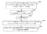
まず、ステップS201では、AC電源がプラスからマイナス、マイナスからプラスへ移行するクロスポイントを発見する。図4において、AD変換後のデジタル値が、0x800000を横切るときがクロスポイントである。クロスポイントを見つけると、AC電源が60Hzである場合は、3周期分のデータを取得するのには、521*3=1563±αのサンプリングデータを取得する(ステップS202)。この3周期分でサンプリングデータにはクロスポイントが6回観測される(ステップS203でYES)。クロスポイントが6回観測されない場合(ステップS203でNO)、ステップ201と同様にクロスポイントを発見する(ステップS204)。クロスポイントを見つけると、AC電源が50Hzである場合は、3周期分のデータを取得するのには、625*3=1875±αのサンプリングデータを取得する(ステップS205)。この3周期分でサンプリングデータにはクロスポイントが6回観測される(ステップS206でYES)。周波数が決定されない場合(ステップS206でNO)、上述のステップを複数回繰返し、それでも決定されない場合は測定エラーとして終了する。 First, in step S201, a cross point where the AC power source shifts from plus to minus and minus to plus is found. In FIG. 4, the cross point is when the digital value after AD conversion crosses 0x800000. When the cross point is found, when the AC power source is 60 Hz, sampling data of 521 * 3 = 1563 ± α is acquired to acquire data for three cycles (step S202). Cross points are observed six times in the sampling data in three cycles (YES in step S203). If the cross point is not observed six times (NO in step S203), the cross point is found in the same manner as in step 201 (step S204). When the cross point is found, if the AC power supply is 50 Hz, sampling data of 625 * 3 = 1875 ± α is acquired to acquire data for three cycles (step S205). Cross points are observed six times in the sampling data in three cycles (YES in step S206). If the frequency is not determined (NO in step S206), the above steps are repeated a plurality of times. If the frequency is still not determined, the process ends as a measurement error.
ここで、マイコン280は、本実施形態では、DCO(ディジタルコントロールドオシレーター)を採用する。DCO回路は、デジタル入力で制御されたLC発振回路であり、多数並列接続されたMOSバラクタのそれぞれに対して"0"か"1"の制御電圧を個別に印加することで、静電容量をデジタル的に変化させる。静電容量の変化に応じて発振周波数を制御する(図10)。水晶発振と異なり、温度、電圧による変動が、例えば、最大3%になる。これら変動を上記したサンプリング数に反映させることが望ましい。AC電源が60Hzの場合には、1563に対して±3%、即ち、1563±47のサンプリングで6回目のクロスポイントが観測される事になる。同様に、AC電源が50Hzの場合は、1875±57のサンプリングで6回目のクロスポイントが観測されることになる(図4)。
Here, the
図6は、10周期分の電流データを取得するためのフローチャートである。周波数によりこの10周期分のサンプリング数もかわり、50Hzでは625*10=6250±188、60Hzでは521*10=5210±157αとなる。まず、クロスポイントを発見(ステップS301)し、データ収集を開始する。アナログデジタル変換されたデータには、システム全体のオフセットが含まれているため、オフセットをとりのぞくことが望ましい。オフセットの値はシステムに何も機器が接続されていない時には、そのデジタル値は、0x800000hとなる。しかしシステム全体から見るとその値は異なり、接続されていない時のデジタル値をYとすると、オフセット値=(0x800000−Y)となる。測定電流の最大を例えば15Aとした時、15Aを流すことできる抵抗負荷を接続したときのデジタル値をXとすると、ゲイン値=(0xffffff−0x800000)/Xとなる。ステップS302で、測定されたVoutに対して、前述で求められたオフセット調整、ゲイン調整を行う。なお、調整後の値 Voutadjは以下の計算式3で求められる。
FIG. 6 is a flowchart for acquiring current data for 10 cycles. Depending on the frequency, the number of samplings for these 10 cycles also changes, and is 625 * 10 = 6250 ± 188 at 50 Hz and 521 * 10 = 5210 ± 157α at 60 Hz. First, a cross point is found (step S301), and data collection is started. Since the analog-digital converted data includes the offset of the entire system, it is desirable to remove the offset. The offset value is 0x800000h when no device is connected to the system. However, when viewed from the whole system, the value is different. When the digital value when not connected is Y, the offset value = (0 × 800000−Y). When the maximum measurement current is 15 A, for example, when a digital value when a resistance load capable of flowing 15 A is connected is X, gain value = (0xffffff−0x800000) / X. In step S302, the offset adjustment and gain adjustment obtained above are performed on the measured Vout. The adjusted value Voutadj is obtained by the following
Voutadj=(Vout+オフセット値)*ゲイン値 ・・・式3 Voutadj = (Vout + offset value) * gain value (3)
なお、ステップS303では、計算されたVoutadjの2乗累積加算を行う。 In step S303, the calculated cumulative Voutadj is squared.
また、Voutadjのべき乗累積加算値 Voutadj2SUMは以下の式で求める。 Further, the power cumulative addition value Voutadj2SUM of Voutadj is obtained by the following equation.
Voutadj2SUM=Σ(Voutadj*Voutadj) ・・・式4
Voutadj2SUM = Σ (Voutadj * Voutadj)
次いで、これを10周期分の2乗累積加算を行う(ステップS304)。 Next, this is subjected to square accumulation for 10 cycles (step S304).
図7は、図6と同様に、10周期分の電圧データを取得するためのフローチャートである。 FIG. 7 is a flowchart for acquiring voltage data for 10 cycles, as in FIG. 6.
まず、クロスポイントを発見(ステップS401)し、データ収集を開始する。電流測定と同様に、無負荷時のオフセットを計測する。また、電源コード3から基準AC100Vを入力して、そのピーク値Zを測定し、ゲイン値=(0xffffff−0x800000)/Zを求める。
First, a cross point is found (step S401), and data collection is started. As with current measurement, the offset at no load is measured. Further, a reference AC100V is input from the
次いで、ステップS402で、測定されたV+、V−に対して、前述で求められたオフセット調整、ゲイン調整を行う。なお、調整後の値 V+adj、V−adjは、以下の計算式5及び式6で求められる。
Next, in step S402, the offset adjustment and gain adjustment obtained above are performed on the measured V + and V-. The adjusted values V + adj and V-adj are obtained by the following
V+adj=((V+)+オフセット値)*ゲイン値 ・・・式5
V―adj=((V−)+オフセット値)*ゲイン値 ・・・式6
V + adj = ((V +) + offset value) *
V−adj = ((V −) + offset value) * gain value (Formula 6)
ステップS403で、AC電源の波高値Vadjを以下の式7で計算する。 In step S403, the peak value Vadj of the AC power source is calculated by the following equation (7).
Vadj=(V+adj)+(0x800000− V−adj) ・・・式7
Vadj = (V + adj) + (0x800000−V−adj)
ステップS404では、計算されたVadjの2乗累積加算を行う。Vadjの2乗累積加算値 Vadj2SUMは以下の式8で求める。 In step S404, the calculated Vadj squared cumulative addition is performed. Vadj2 square cumulative addition value Vadj2SUM is obtained by the following equation (8).
Voutadj2SUM=Σ(Voutadj*Voutadj) ・・・式8
Voutadj2SUM = Σ (Voutadj * Voutadj)
次いで、これを10周期分の2乗累積加算を行う(ステップS405)。 Next, this is subjected to square accumulation for 10 cycles (step S405).
次に、図8に示すフローチャートによる皮相電力を求める手順に関する説明の前に、図9に示す有効電力を求める点について説明する。図9は、有効電力を求めるためのフローチャートである。ステップS403で得られた電圧VadjとステップS302で得られた電流Voutadjを乗算して電力を計算する(ステップS601)。これを10周期分求めて累積加算を行う(ステップS602、603)。前述したように、周波数によりこの10周期分のサンプリング数もかわり、50Hzでは625*10=6250+α、60Hzでは521*10=5210+αであり、累積加算値VAadjSUMをサンプリング数で割る(ステップS604)。 Next, the point of obtaining the active power shown in FIG. 9 will be described before the description of the procedure for obtaining the apparent power according to the flowchart shown in FIG. FIG. 9 is a flowchart for obtaining active power. Power is calculated by multiplying the voltage Vadj obtained in step S403 by the current Voutadj obtained in step S302 (step S601). This is obtained for 10 cycles and cumulative addition is performed (steps S602 and 603). As described above, the number of samplings for these 10 cycles varies depending on the frequency, and 625 * 10 = 6250 + α at 50 Hz and 521 * 10 = 5210 + α at 60 Hz, and the cumulative added value VAadjSUM is divided by the number of samplings (step S604).
こうして得られたVAadjSUMに変換係数を乗算して有効電力Wを求める(ステップS605)。ここで変換係数は、たとえば、抵抗負荷を実際し接続したときの値を測定し(WL)、抵抗負荷が100Ωのときの有効電力は、100V*100V/100Ω=100Wであるため、WL/100が変換係数となる。 The active power W is obtained by multiplying the VAadjSUM thus obtained by the conversion coefficient (step S605). Here, the conversion coefficient is, for example, measured when a resistance load is actually connected (WL), and the effective power when the resistance load is 100Ω is 100V * 100V / 100Ω = 100 W, so WL / 100 Is the conversion coefficient.
図8は皮相電力を求めるためのフローチャートである。ステップS304で得られた10周期分の電流2乗積算値Voutadj2SUMをサンプル数で割ってVoutadj2SUMSAMPを求める(ステップS501)。同様に、ステップS406で得られた10周期分の電圧2乗積算値Vadj2SUMをサンプル数で割ってVadj2SUMSAMPを求める(ステップS503)。Voutadj2SUM、SAMPVadj2SUMSAMの平方根を求めて、変換係数を乗算することにより、電流実効値、電圧実効値を求めることができる(ステップS502、ステップS504)。ここで電流変換係数であるが、抵抗負荷、例えば10Ωを接続した場合の値を測定し、測定された値をISとすると、100V/10Ω=10Aであることから、IS/10が電流変換係数となる。電圧変化係数は、無負荷時に測定された値をVSとするとVS/100が電圧変換係数となる。電流実効値と電圧実効値を乗算することで皮相電力VAを求めることができる(ステップS505)。 FIG. 8 is a flowchart for obtaining the apparent power. Voutad2SUMMSAMP is obtained by dividing the current square integrated value Voutadj2SUM for 10 cycles obtained in step S304 by the number of samples (step S501). Similarly, Vadj2SUMMSAMP is obtained by dividing the voltage square integrated value Vadj2SUM for 10 cycles obtained in step S406 by the number of samples (step S503). By obtaining the square root of Voutadj2SUM and SAMPVadj2SUMSAM and multiplying by the conversion coefficient, the current effective value and the voltage effective value can be obtained (steps S502 and S504). Here, the current conversion coefficient is measured when a resistance load, for example, 10Ω is connected, and when the measured value is IS, it is 100V / 10Ω = 10A. Therefore, IS / 10 is a current conversion coefficient. It becomes. The voltage change coefficient is VS / 100 as the voltage conversion coefficient when the value measured at no load is VS. The apparent power VA can be obtained by multiplying the current effective value and the voltage effective value (step S505).
なお、上述した消費電力測定装置としての図1等に示すテーブルタップ100は、例えば、図示しないが、パーソナルコンピュータや携帯端末等の外部端末(情報処理装置)に直接又は中継装置を経由して通信可能に接続されて消費電力測定システム(消費電力管理システムを含めてもよい)を構成する。即ち、消費電力測定装置によって測定された消費電力に基づく消費電力情報(消費電力又はそれに関する情報、消費電力に基づく消費電力量に関する消費電力量情報を含む)は、消費電力測定装置内の通信モジュールより外部端末へ送信される。一方、消費電力情報を受け取った外部端末側では、その消費電力情報をディスプレイ等の表示手段に表示する。これにより、ユーザは、消費電力測定機能を備えたテーブルタップ100に接続されている1つ又は複数の電気機器の消費電力を効率的に管理することができる。なお、本実施形態のテーブルタップ100は、コンセントを4口設けた例を説明したが、1口でもよいし、2〜3口、あるいは5口以上設けてもよい。
The
ここで、上述したテーブルタップ100に実装される電流測定手段の少なくとも一部を構成する電流センサ24としては、例えば、本実施形態では、詳細は後述するが、コンセント基板220上の各パターン210と各コンセントプラグ200a,200b,200c,200dとの間を流れる被測定電流の流れ方向を別の方向に変更する電流方向変更領域と、電流方向変更領域により電流方向が変更された被測定電流によって生じる磁気を検知する磁気検知素子とを備えるものを用いることが好ましい。
Here, as the
以下、本発明の消費電力測定装置において、電気機器の消費電力を測定するにあたり、コンセントとプラグとを接続した導体(具体的には、基板上の接続配線であって、例えば、図1における配線パターン210等)を流れる電流値を測定するのに最適な電流測定装置において詳細に説明するが、本発明は以下の構成に限定されるものではない。
Hereinafter, in the power consumption measuring apparatus of the present invention, when measuring the power consumption of an electrical device, a conductor (specifically, a connection wiring on a substrate, for example, the wiring in FIG. The current measuring apparatus optimal for measuring the current value flowing through the
導体を流れる電流から発する周回磁界を磁気検知素子で直接検知する場合には、次のような課題がある。即ち、被測定電流が流れる導体に隣接して、異なる相の電流が流れる導体が平行に配置されている場合に、電流が流れる方向と直角方向の成分となる周回磁界を対象にすると、隣接する電流線からの磁界が加わり、十分な測定精度が得られないことがある。これらの干渉を磁気シールドで防止するとしても、被測定電流からの磁束が磁場自体を乱してしまう虞れや、シールド部材の磁気飽和の心配があり、効果的な対策を施すことは難しくなる。 In the case of directly detecting the circular magnetic field generated from the current flowing through the conductor by the magnetic detection element, there are the following problems. In other words, when conductors through which currents of different phases are arranged in parallel and adjacent to the conductor through which the current to be measured flows, they are adjacent when a circular magnetic field having a component perpendicular to the direction of current flow is targeted. A magnetic field from a current line is applied, and sufficient measurement accuracy may not be obtained. Even if these interferences are prevented by the magnetic shield, there is a possibility that the magnetic flux from the current to be measured may disturb the magnetic field itself and there is a concern about the magnetic saturation of the shield member, making it difficult to take effective measures. .
そこで、上述の課題を解消し、異なる相の電流が平行して流れる設置環境であっても、磁気シールドに頼らず、被測定電流の測定精度を安定して確保できる電流測定方法及び電流測定装置であれば、本発明の消費電力測定装置に好適である。 Accordingly, a current measuring method and a current measuring apparatus that can solve the above-described problems and can stably ensure the measurement accuracy of the current to be measured without depending on the magnetic shield even in an installation environment in which currents of different phases flow in parallel. If so, it is suitable for the power consumption measuring apparatus of the present invention.
以下、本発明の消費電力測定装置において好適に実装される電流測定装置を図示の実施例に基づいて詳細に説明する。なお、本発明では、被測定電流が流れる導体の一部に被測定電流の流れる方向を主方向から別の方向に変更する電流方向変更領域を設けることに1つの特徴がある。さらに、本発明では、電流方向変更領域によって流れる方向を変更された被測定電流によって生じた磁界を磁気検知素子によって検知することに特徴がある。 Hereinafter, a current measuring device suitably mounted in the power consumption measuring device of the present invention will be described in detail based on the illustrated embodiment. One feature of the present invention is that a current direction changing region for changing the direction in which the current to be measured flows from the main direction to another direction is provided in a part of the conductor through which the current to be measured flows. Furthermore, the present invention is characterized in that a magnetic field generated by a current to be measured whose direction of flow is changed by a current direction changing region is detected by a magnetic detection element.
<実施例1>
図12は被測定電流に対する電流測定を行う実施例1の基本的な構成図である。一次導体1には検知対象の被測定電流Iが流れ、一次導体1は例えばプリント基板上の銅箔パターン又は銅板で形成されたバスバー等の形態とされている。
<Example 1>
FIG. 12 is a basic configuration diagram of the first embodiment for measuring current with respect to the current to be measured. A current to be measured I to be detected flows through the
一次導体1のほぼ中央には、電流の遮断を部分的に行うために、非導電領域である円形の貫通孔2が設けられており、このため被測定電流Iの一部は図13に示すようにこの貫通孔2の両側において外側を対称的に回り込む迂回電流Iaとなっている。説明の便宜のために、一次導体1に座標軸を設定し、貫通孔2の中心を原点Oとして、被測定電流Iが流れる主方向をY軸、その直交軸である幅方向をX軸、厚み方向をZ軸とする。
A circular through
一次導体1上には、一方向にのみ磁界検知感度を有する磁気検知素子3が配置されている。磁気検知素子3の検知部4をY軸方向が磁界検知方向となるようにし、検知部4の中心位置は、貫通孔2の中心よりもX軸方向に距離dx、Y軸方向にはX軸を挟んで距離dyずらした個所に配置されている。
On the
本来、電流により発生する磁束は電流方向と直交する方向を向くので、一次導体1の貫通孔2の影響がない個所では、被測定電流Iは主方向であるY軸方向に流れる。従って、図13に示す磁界ベクトル成分Hc0のように、一次導体1の幅w内ではX軸方向のベクトル成分Hxしか持たない磁場となる。
Originally, the magnetic flux generated by the current is directed in a direction perpendicular to the current direction, so that the current to be measured I flows in the Y-axis direction, which is the main direction, in a place where the through
しかし貫通孔2の近傍では、迂回電流IaはY軸方向に対し傾くことから、この迂回電流Iaにより貫通孔2の両側で磁場が歪んだ磁界ベクトル成分Hc1が発生する。つまり、迂回電流Iaの傾き部分においては、Y軸方向のベクトル成分Hy及びX軸方向のベクトル成分Hxが発生する。ベクトル成分Hyとベクトル成分Hxのベクトル和は被測定電流Iの大きさに比例し、貫通孔2のY軸の正負両側では電流方向が対称形のため、ベクトル成分HyはX軸を挟んで対称となり、極性は逆になる。
However, in the vicinity of the through
また図12に示すように、異なる相の電流が流れる一次導体1’が近接し、近接電流I’の方向が被測定電流Iと平行していても、近接電流I’による磁界ベクトル成分はX軸方向のみの成分であり、Y軸方向成分を持たない。検知部4の磁界検知方向をY軸方向とすると、磁気検知素子3は近接電流I’による磁界による干渉は受けず、迂回電流Iaのベクトル成分Hyのみを検知できる。従って、このベクトル成分Hyを校正して換算すれば、被測定電流Iの電流量を求めることができる。
As shown in FIG. 12, even if the
使用する磁気検知素子3として、X軸方向の磁界ベクトル成分Hxを検知することは望ましくない。従って、指向性の高い磁気インピーダンス素子や直交フラックスゲート素子が好適であり、実施例1では磁気インピーダンス素子を用い、Y軸方向にのみ磁界検知が可能とされている。検知部4として磁性薄膜のパターンが磁界検知方向のY軸方向につづら折りにより並列され、両端の電極5にMHz帯の高周波パルスを印加し、磁界の変化による検知部4の両端からの電圧振幅変化をセンサ信号として得ている。図示は省略しているが、検知部4の動作には、バイアス磁界が必要となるものがあり、必要に応じて近くにバイアス磁石の設置又はバイアスコイルを巻き付けて電流を流して設定する。
It is not desirable to detect the magnetic field vector component Hx in the X-axis direction as the
図14に示すように、一次導体1に対する磁気検知素子3の検知部4の高さhは、一次導体1と磁気検知素子3の位置関係を保持する構造上、必要なスペースと空間距離、沿面距離等の絶縁耐圧の関係で決められる。
As shown in FIG. 14, the height h of the
図15は電流測定装置として機能する検知回路100Aの構成図を示す。CRパルス発振回路30に対しブリッジを構成する抵抗Rに、磁気検知素子3の検知部4が接続されている。検波回路31は、検知部4の検知信号である両端電圧からの振幅変化を取り出して増幅回路32へ出力する。増幅回路32は、振幅変化を増幅して出力する。推定回路33は、増幅回路32の出力から被測定電流の電流量を推定する回路である。
FIG. 15 shows a configuration diagram of a detection circuit 100A that functions as a current measuring device. The
図16、図17は貫通孔2による迂回電流Iaに係わるY軸方向の磁界成分Hyのシミュレーションの結果を示している。一次導体1はX軸方向の幅w=10mm、Z軸方向の厚さt=70μmの断面で、Y軸方向に計算上は無限長とした十分に長い銅板であり、X軸方向の中央に貫通孔2を穿けてある。検知部4は一次導体1から1.6mmの高さhに固定し、Y軸方向に被測定電流Iを1アンペア(A)流した際のY軸方向の磁界ベクトル成分Hyの変化を調べた。
16 and 17 show the simulation results of the magnetic field component Hy in the Y-axis direction related to the bypass current Ia through the through
図16は貫通孔が2mmの場合、図17は3mmの場合におけるY軸方向磁界のベクトル成分Hyの磁界分布の計算結果を等高線の分布として示している。座標はX≧0、Y≧0の第1象限で、ベクトル成分Hyの頂点を100%として、10%刻みで等高線を描いている。他の象限ではX軸又はY軸に関し対称な磁界分布が形成され、第3象限は第1象限と同一極性で、第2、第4象限は第1象限と逆極性の磁場が形成される。 16 shows the calculation result of the magnetic field distribution of the vector component Hy of the magnetic field in the Y-axis direction when the through hole is 2 mm, and FIG. 17 shows the distribution of contour lines. The coordinates are the first quadrant of X ≧ 0 and Y ≧ 0, and the contours are drawn in 10% increments with the vertex of the vector component Hy being 100%. In the other quadrants, a magnetic field distribution symmetric with respect to the X axis or the Y axis is formed, the third quadrant has the same polarity as the first quadrant, and the second and fourth quadrants have a magnetic field having the opposite polarity to the first quadrant.
図16、図17から磁界が最大となるピーク位置は、貫通孔2から約45度方向にあり、直径2mmの貫通孔2では(X、Y)=(1.5mm、1.625mm)、3mmの貫通孔2では(X、Y)=(1.75mm、1.75mm)辺りにある。これらの磁界のピーク位置での磁界成分Hyは、それぞれ電流1アンペア(A)に対して、Hy=25.6mガウス(G)、Hy=47.9mガウス(G)となっている。
16 and 17, the peak position where the magnetic field is maximized is in the direction of about 45 degrees from the through
図18は貫通孔2の直径とY軸方向の磁界ベクトル成分Hyのピーク位置の関係のグラフ図である。図16、図17に示す等高線図では図示を省略しているが、直径1mm、4mmでの結果も併せて記載している。図18から分るように、貫通孔2の直径の大きさはピーク部の位置に殆ど依存することはない。幅w=5mmでの貫通孔2の直径1mmの結果も併せて考えると、実用的な一次導体1の使用範囲では、ベクトル成分Hyのピークの範囲は、X、Y軸方向共に1〜2mm程度であると云える。
FIG. 18 is a graph showing the relationship between the diameter of the through
また、ピーク位置から10%下がった90%の範囲が、半径0.5mm程度のサークルとなっていることから、設計的には図1の距離dx、dyは共に0.5〜2.5mmの範囲で、この範囲に磁気検知素子3の検知部4が掛かるようにすればよい。
Further, since 90% of the
図19は一次導体1の貫通孔2の径とY軸方向のベクトル成分Hyのピーク値とのグラフ図であり、径が大となるにつれて、2次関数的にベクトル成分Hyが大きくなってゆくことが分かる。つまり、図12で示す距離dx=1.5mm、dy=1.5mm辺りに、磁気検知素子3の検知部4を固定し、貫通孔2の径の大きさを変えるだけで、数倍もの測定レンジを選択できることが可能となる。
FIG. 19 is a graph of the diameter of the through
図12においては、磁気検知素子3はXY平面上の第1象限に設けているが、対称性から当然のことながら、その他の象限に配置することもできる。
In FIG. 12, the
図20は変形例を示し、貫通孔2’を貫通孔2のある原点OからX軸方向に対して45度方向に設けて、その中間位置に磁気検知素子3を配置することで、両貫通孔2、2’による迂回電流Iaによる効果を重ねY軸方向成分の磁界を増加し、感度を上げている。2つの貫通孔2、2’は同一の大きさである必要はなく、更に貫通孔2の数を増やすこともできるし、設置する角度位置は電流の検知仕様に応じて設計すればよい。
FIG. 20 shows a modification, in which a through
電流を迂回させる手段としては、貫通孔2だけではなく切欠孔を用いることにより非導電領域を形成し、大小の電流に対応させることができる。例えば、図21に示すように、一次導体1の幅方向の端部に切欠孔8を設けることでも迂回電流を生成できる。大電流により迂回電流による磁界を抑制したい場合には、この構成が好適である。
As a means for bypassing the current, not only the through-
また、逆に図22に示すように切欠孔8を深くし、迂回電流を集中させ、Y軸方向成分の磁界を大きくし、小電流に対応させることも可能である。更に、図23に示すように反対側からの端部からも切欠孔8をずらして設けることで、更に迂回電流を強めて、より小さな電流にも対応させることができる。
On the contrary, as shown in FIG. 22, it is possible to deepen the
<実施例2>
図24は実施例2の構成図である。例えば、厚さ1.6mmのガラスエポキシ材のセンサ基板11の片面に、X軸方向の幅10mm、Z軸方向の厚さ70μm、Y軸方向の長手方向50mmの銅パターンから成る一次導体12が設けられている。そして、一次導体12のX軸方向の中央に例えば直径2mmの貫通孔13がエッチングにより形成されている。センサ基板11の他面には、図25と同様の位置に、一体型の磁気検知ユニット14が配置され、半田付けのための電極15a〜15bがセンサ基板11上に引き出されている。
<Example 2>
FIG. 24 is a configuration diagram of the second embodiment. For example, the
磁気検知ユニット14には磁気インピーダンス素子が用いられ、Fe−Ta−C系の磁性薄膜から成る検知部16は、それぞれ例えば幅18μm、厚さ2.65μm、長さ1.2mmの細長い11本のパターンが並列に配置されている。そして、検知部16の磁界検知方向はY軸方向のみとされている。
A magnetic impedance element is used for the
検知部16の位置は、貫通孔13の中心からX軸及びY軸方向に距離dx=1.5mm、dy=1.5mmだけオフセットされて配置されている。検知部16の複数本の磁性薄膜パターンは、図示は省略しているが電気的にはつづら折りで直列につながれて、両端はそれぞれの電極に接続され、センサ基板11上の電極15a、15bに半田接合され、図示しないセンサ回路に接続されている。図24では、電極15a→15bの流れにより高周波パルスを印加する。
The position of the
磁気検知ユニット14の磁性薄膜にはX軸方向の幅方向に磁化容易軸が設けられており、高周波のパルスを磁性薄膜のパターンに通電することで、外部磁界によりインピーダンスが変化し、磁気検知ユニット14の両端電圧を振幅検波によりセンサ信号に変換する。
The magnetic thin film of the
平行して流れる被測定電流I以外の電流の影響評価では、図24に示すように、一次導体12から10mmの間隔をおいて直径2mmの銅棒18を並行に配置し、10Armsの50Hzの電流I’を流して、一次導体12には電流を流さない条件で測定した。すると、磁気検知ユニット14では銅棒18を流れる電流I’の影響は観測されず、ノイズレベル以下(10mVpp以下)であった。
In the evaluation of the influence of currents other than the current I to be measured flowing in parallel, as shown in FIG. 24, a
隣接する平行な電流線からの磁界はX軸又はZ軸方向となり、Y軸方向の成分は持たないことと、磁気インピーダンス素子がX軸方向には感度を持たないことが効果的に作用し、隣接の電流による磁界の影響は問題とはならないレベルであることが確認された。 The magnetic field from the adjacent parallel current line is in the X-axis or Z-axis direction, and it has an effective effect that it has no component in the Y-axis direction and that the magneto-impedance element has no sensitivity in the X-axis direction, It was confirmed that the influence of the magnetic field due to the adjacent current is at a level that does not cause a problem.
この磁気検知ユニット14は5Vの5MHzのパルス駆動では、図25に示すように磁界に対してV字のインピーダンス変化の特性を示し、感度の良い傾きの個所を利用している。そのためには、図24に示すように磁気検知ユニット14の背面にバイアス用磁石17を配置して、検知部16に10ガウス(G)程度のバイアス磁界が掛かるように設定している。直線性の良好な範囲は、この磁気検知ユニット14の場合ではバイアス動作点を挟んで±3ガウス(G)程度である。
In the 5 V pulse drive of 5 V, the
図26は一次導体1にAC電流(50Hz)を0.1〜40Armsまで可変で通電させて、電流測定したデータを示している。10Armsは28.28Appの正弦波であり、そのときの磁界はシミュレーション結果から、724mGppとなる。図15はこの10Armsを基準に理想値と実測値の誤差を示し、5V電源で10Arms時に1Vppとなるように調整したため、上限は40Armsとした。精度として、0.2Arms以上で±1%以内の誤差が保証される。
FIG. 26 shows data obtained by measuring the current when the
貫通孔13の直径を2mmとし、磁気検知ユニット14の直線性範囲が6ガウス(G)の特性のものを使用した場合では、80Arms強の個所で越えてしまう。仮に、200Armsまで対応させる場合では、貫通孔13の直径を1mmにするだけで、磁気検知ユニット14に掛かる磁界は1/3になり、270Armsのような大電流にも同じレイアウトで可能になる。また、逆に小電流の仕様には、貫通孔13を大きくするだけで対応できる。
In the case where the diameter of the through
実施例2では、一次導体12をセンサ基板11上に配置している例を想定している。しかし、図27の変形例に示すように、一次導体が銅板から成るバスバー19の場合は、図24の形態から一次導体12を除いたものをセンサ基板20の上にモジュール化することもできる。この場合には、バスバー19に穿けた貫通孔21にセンサ基板20を位置合わせして、センサ基板20をバスバー19に貼り合わせなどにより固定して使用することが可能である。なお、22はセンサ基板20上に設けられた回路素子、23は磁気検知ユニット14の信号を引き出す信号線である。
In the second embodiment, it is assumed that the
このような構成とすることにより、予めバスバー19を布設した後においても、磁気検知ユニット14をモジュール化してバスバー19に組み付けることにより容易に組立てが可能となる。
With such a configuration, even after the
なお、上述の各実施例においては、貫通孔、切欠孔による非導電領域を設けて電流を迂回させたが、必ずしも孔部ではなく、絶縁材料を配置することによっても電流を迂回させることができる。 In each of the above-described embodiments, the current is diverted by providing a non-conductive region with a through hole and a notch hole, but the current can be diverted by arranging an insulating material instead of the hole. .
<実施例3>
特開2006−184269号公報によれば、2個の磁気検知素子を使用することで、差動検知により外乱磁界を回避しようとする提案がなされている。この特許文献では、被測定電流による磁界検知を単一の磁気センサで検知する場合の外部磁界の影響を回避するために、一次導体としてのバスバーの中央部に開口部を形成して被測定電流を分流している。そして、開口部内に2つの導体部近傍に電流からの磁界がそれぞれ逆相になるようにそれぞれ磁気検知素子を配し、差動増幅によりバスバーから発生する磁界のみを検知している。
<Example 3>
According to Japanese Patent Laid-Open No. 2006-184269, a proposal has been made to avoid a disturbance magnetic field by differential detection by using two magnetic detection elements. In this patent document, in order to avoid the influence of the external magnetic field when the magnetic field detection by the measured current is detected by a single magnetic sensor, an opening is formed in the central portion of the bus bar as the primary conductor to measure the measured current. Is diverted. In the opening, magnetic detection elements are arranged in the vicinity of the two conductors so that the magnetic fields from the currents have opposite phases, and only the magnetic field generated from the bus bar is detected by differential amplification.
しかしながら、この方法でも一様な磁界に対する影響は排除できても、隣接して電流線が平行して流れる場合には、2つの磁気検知素子にはその外乱となる磁界が等しく印加されず、結局は磁気シールドが不可欠となる。この点を解決する方法として、非導電領域を一次導体に設けるとともに、非導電領域の近傍に1つの磁気検知素子を設けることを実施例1、2で提案した。ここで、磁気検知素子は複数であってもよい。そこで、実施例3では、複数の磁気検知素子を設ける案について説明する。 However, even if this method can eliminate the influence on the uniform magnetic field, if the current lines flow adjacently, the two magnetic sensing elements are not equally applied with the disturbance magnetic field. A magnetic shield is indispensable. As a method for solving this problem, the first and second embodiments have proposed that a non-conductive region is provided in the primary conductor and that one magnetic sensing element is provided in the vicinity of the non-conductive region. Here, a plurality of magnetic sensing elements may be provided. Therefore, in the third embodiment, a plan for providing a plurality of magnetic sensing elements will be described.
図28は被測定電流に対する電流測定を行う実施例3の基本的な電流センサの構成図である。一次導体1には検知対象の被測定電流Iが流れ、一次導体1は例えばプリント基板上の銅箔パターン又は銅板で形成されたバスバー等の形態とされている。
FIG. 28 is a configuration diagram of a basic current sensor of Example 3 that performs current measurement on a current to be measured. A current to be measured I to be detected flows through the
一次導体1のほぼ中央には、電流の遮断を部分的に行うため非導電領域である円形の貫通孔2が設けられており、このため被測定電流Iの一部は図29に示すようにこの貫通孔2の両側において外側を対称的に回り込む迂回電流Iaとなっている。説明の便宜のために、一次導体1に座標軸を設定し、貫通孔2の中心を原点Oとして、被測定電流Iが流れる主方向をY軸、その直交軸である幅方向をX軸、厚み方向をZ軸とする。
Near the center of the
一次導体1上には、2つの磁気検知素子3a、3bがY軸方向に向けて直列的に配置されて差動検知が行われる。磁気検知素子3a、3bの検知部4a、4bをY軸方向が磁界検知方向となるようにし、検知部4a、4bの中心位置は、貫通孔2の中心よりもX軸方向に距離dx、Y軸方向にはX軸を挟んで距離dyずらした個所に配置されている。図28に示すように、異なる相の電流が流れる一次導体1’が近接し近接電流I’の方向が被測定電流Iと平行していても、近接電流I’の磁束Fによる磁界の影響はX軸方向のベクトル成分となり、Y軸方向成分を持たない。検知部4a、4bの磁界検知方向をY軸方向に取ると、磁気検知素子3a、3bは近接電流I’による磁界による干渉は受けず、被測定電流Iのベクトル成分Hyのみを検知できる。従って、このベクトル成分Hyを校正して換算すれば、被測定電流Iの電流量を求めることができる。
On the
使用する磁気検知素子3a、3bとして、X軸方向の磁界ベクトル成分Hxを検知することは望ましくないため、指向性の高い磁気インピーダンス素子や直交フラックスゲート素子が好適であり、実施例1では磁気インピーダンス素子を用いている。検知部4a、4bとして磁性薄膜のパターンが磁界検知方向のY軸方向につづら折りにより並列され、両端の電極5にMHz帯の高周波パルスを印加し、磁界の変化による検知部4a、4bの両端からの電圧振幅変化をセンサ信号として得ている。
Since it is not desirable to detect the magnetic field vector component Hx in the X-axis direction as the
図30に示すように、一次導体1に対する磁気検知素子3a、3bの検知部4a、4bの高さhは、一次導体1と磁気検知素子3a、3bの位置関係を保持する構造上、必要なスペースと空間距離、沿面距離等の絶縁耐圧の関係で決められる。
As shown in FIG. 30, the height h of the
図31は検知回路100Aの構成図を示し、CRパルス発振回路30に対しブリッジを構成する抵抗Rに、磁気検知素子3a、3bの検知部4a、4bが接続されている。検知部4a、4bの両端電圧からの振幅変化を検波回路31により取り出した後に、差動増幅回路32で検知部4a、4bの出力に対し差動増幅が行われて、電流センサとしての出力を得る。
FIG. 31 shows a configuration diagram of the detection circuit 100A. The
この場合に、検知部4a、4bの出力は、感度が同じでX軸を挟んで対称な位置にあれば絶対値は同じになり、極性が異なるため、差動的に検知すると、出力は検知部4a又は4bの絶対値の2倍となる。また、外来の磁界ノイズは狭い範囲にある検知部4a、4bでは同相となり、検知部4a、4bの出力を差動的に捉えることにより、磁界ノイズは相殺されて、電流センサの出力に重畳されることはなく、迂回電流のベクトル成分Hyのみが測定されることになる。なお、磁気検知素子の出力を差動的に検知するには、少なくとも2個の検知部を用いればよい。
In this case, the outputs of the
なお、図31と図15とを比較すれば明らかなように、ブリッジ回路を形成している4つの抵抗が検知部に置き換わることになる。たとえば、3つの検知部を採用するのであれば、4つある抵抗のうちの3つの抵抗が検知部に置換される。さらに、4つの検知部を採用するのであれば、すべての抵抗が検知部に置換されることになる。 As apparent from a comparison between FIG. 31 and FIG. 15, the four resistors forming the bridge circuit are replaced with the detection unit. For example, if three detection units are employed, three of the four resistors are replaced with the detection unit. Furthermore, if four detection units are employed, all the resistances are replaced with detection units.
図28においては、磁気検知素子3a、3bはXY平面上の第1、第4象限にそれぞれ設けているが、対称性から当然のことながら、その他の象限に隣接して配置することもできる。
In FIG. 28, the
図32はこの場合の変形例を示し、磁気検知素子3aは第1象限に、磁気検知素子3bは第2象限に設け、Y軸に対して対称的に配置した場合においても同様の結果が得られる。迂回電流Iaによる磁界ベクトル成分Hc1は第1象限と第2象限においてY軸に関して対象ともなっている。従って、磁気検知素子3a、3bを第1象限、第2象限にそれぞれ配置し、絶対値が等しく極性が逆のY軸方向のベクトル成分Hyをそれぞれ検知することができる。この場合においては、隣接して平行する電流線の影響は僅かに受けるが、磁気検知素子3同士の間隔が狭いために、ほぼ磁界ノイズを差動検知により相殺することができる。
FIG. 32 shows a modification in this case, and the same result is obtained even when the
<実施例4>
磁気検知素子である磁気インピーダンス素子や直交フラックスゲートセンサ等のように、磁気飽和や直線性の点で、検知磁界範囲を或る範囲内で管理しなくてはならない場合には、一次導体1の貫通孔2の径だけで測定レンジを調整できることが好ましい。
<Example 4>
When the detection magnetic field range must be managed within a certain range in terms of magnetic saturation and linearity, such as a magnetic impedance element or an orthogonal fluxgate sensor which is a magnetic detection element, the
図33は実施例4の電流センサの構成図である。図28における磁気検知素子3、4の検知部4a、4bの距離は短いことから、同一の素子基板6にX軸に関して対称に配置した磁気検知素子3a、3bを一体型として取り付けた磁気検知ユニット7とされ、性能のばらつきが抑制可能となっている。
FIG. 33 is a configuration diagram of the current sensor of the fourth embodiment. Since the distance between the
図34の変形例に示すように、一次導体1のX軸の正の領域だけ使う発想で、幅方向の端部に切欠孔8を設けることでも迂回電流を利用できる。この切欠孔8によっても、図28に示すように貫通孔2を設けた場合と同様に測定が可能である。なお、迂回電流をX軸に関して対称的に流すためには、切欠孔8はX軸に関して対称形であることが必要である。
As shown in the modification of FIG. 34, the idea is to use only the positive region of the X-axis of the
図35は他の変形例の構成図である。4個の磁気検知素子3a〜3dを一体化した磁気検知ユニット7において、第1、第2、第3、第4象限にそれぞれ検知部4a、4b、4c、4dを配置し、4素子によりブリッジ構成として動作させると、更にS/Nを向上させることができる。このように、貫通孔2の両側に検知部4a〜4dをX軸、Y軸に対称に配置すると、ベクトル成分HyがX軸、Y軸にそれぞれ対称となる。
FIG. 35 is a configuration diagram of another modification. In the
従って、X軸に関して検知部4aと4dの出力を差動検知、検知部4bと4cの差動検知、Y軸に関して検知部4aと4bの差動検知、検知部4dと4cの差動検知を同時に行うことができ、これらの検知結果の平均を求めれば更に測定精度が向上する。
Therefore, differential detection of the outputs of the
<実施例5>
図36は実施例3の電流センサの構成図である。厚さ1.6mmのガラスエポキシ材のセンサ基板11の片面に、X軸方向の幅10mm、Z軸方向の厚さ70μm、Y軸方向の長手方向50mmの銅パターンから成る一次導体12が設けられている。そして、一次導体12のX軸方向の中央に直径2mmの貫通孔13がエッチングにより形成されている。センサ基板11の他面には、図33と同様の位置に、一体型の磁気検知ユニット14が配置され、半田付けのための電極15a〜15cがセンサ基板11上に引き出されている。
<Example 5>
FIG. 36 is a configuration diagram of the current sensor according to the third embodiment. A
磁気検知ユニット14には磁気インピーダンス素子が用いられ、Fe−Ta−C系の磁性薄膜から成る検知部16a、16bは、それぞれ幅18μm、厚さ2.65μm、長さ1.2mmの細長い11本のパターンが並列に配置されている。そして、検知部16a、16bの磁界検知方向はY軸方向とされている。
The
検知部16a、16bの位置は、貫通孔13の中心からX軸方向に距離dx=1.5mmだけオフセットされ、検知部16a、16bの中心間隔は、dy=3mmとし、貫通孔13の中心Oから幅方向に延びるX軸に対して対称的に配置されている。
The positions of the
検知部16a、16bの複数本の磁性薄膜パターンは、図示は省略しているが電気的にはつづら折りで直列につながれて、両端はそれぞれの電極に接続され、センサ基板11上の電極15a〜15cに半田接合され、図示しないセンサ回路に接続されている。図36では、センサ基板11に引き出された電極15a→15c及び電極15b→15cの流れにより高周波パルスを印加する。
Although not shown, the plurality of magnetic thin film patterns of the
磁気検知ユニット14はX軸方向の幅方向に磁化容易軸を設けておき、高周波のパルスを磁性薄膜のパターンに通電することで、外部磁界によりインピーダンスが変化し、磁気検知ユニット14の両端電圧を振幅検波によりセンサ信号に変換する。
The
平行して流れる被測定電流I以外の電流の影響評価では、一次導体12から10mmの間隔を離して直径2mmの銅棒18を並列に配置し、10Armsの50Hzの電流I’を流して、一次導体12には電流を流さない条件で測定した。すると、磁気検知ユニット14では銅棒18を流れる電流I’の影響は観測されず、ノイズレベル以下(10mVpp以下)であった。隣接する平行な電流線からの磁界はX又はZ軸方向となり、Y軸方向の成分は持たないことと、検知部16a、16bと隣接する銅棒18との距離が等しいことで差動除去機能が効果的に働き、ノイズ的な磁界の影響もほぼ完全に除去できていることが確認された。
In the evaluation of the influence of currents other than the current I to be measured flowing in parallel, a
実施例5では、一次導体12をセンサ基板11上に配置している例を想定した。しかし、図37の変形例に示すように一次導体が銅板から成るバスバー19の場合は、図36の形態から一次導体12を除いたものをセンサ基板20の上にモジュール化することもできる。この場合には、バスバー19に穿けた貫通孔21にセンサ基板20を位置合わせして、センサ基板20をバスバー19に貼り合わせなどにより固定して使用することが可能である。なお、22はセンサ基板20上に設けられた回路素子、23は磁気検知ユニット14の信号を引き出す信号線である。
In Example 5, the example which has arrange | positioned the
このような構成とすることにより、予めバスバー19を布設した後においても、磁気検知ユニット14をモジュール化してバスバー19に組み付けることにより容易に組立てが可能となる。
With such a configuration, even after the
なお、上述の各実施例においては、貫通孔、切欠孔による非導電領域を設けて電流を迂回させたが、必ずしも孔部ではなく、絶縁材料を配置することによっても電流を迂回させることができる。そして、これらの非導電領域はX軸に関しその両側で形状が対称であることが必要である。 In each of the above-described embodiments, the current is diverted by providing a non-conductive region with a through hole and a notch hole, but the current can be diverted by arranging an insulating material instead of the hole. . These non-conductive regions need to be symmetrical on both sides with respect to the X axis.
<実施例6>
実施例1ないし実施例5では、方向変更領域として非導電領域を採用した。つまり、実施例1ないし実施例5は、電流が非導電領域を迂回して流れることで発生する歪み磁界を検知し、検知した磁界から電流量を推定する発明である。実施例1ないし実施例5において共通した概念は、電流が非直線的に流れることを促進する領域を一次導体に設けることである。つまり、電流の流れる方向を曲げることができるのであれば、必ずしも非導電領域である必要はない。そこで、実施例6では、方向変更領域についての他の例について説明する。
<Example 6>
In Examples 1 to 5, a non-conductive region is employed as the direction change region. That is, the first to fifth embodiments are inventions that detect a distorted magnetic field generated when a current flows around a non-conductive region and estimate the amount of current from the detected magnetic field. A common concept in the first to fifth embodiments is to provide a region in the primary conductor that promotes a non-linear flow of current. In other words, the non-conductive region is not necessarily required as long as the current flowing direction can be bent. Accordingly, in the sixth embodiment, another example of the direction change area will be described.
図38は被測定電流に対する電流測定を行う実施例6の基本的な電流センサの構成図である。一次導体1には検知対象の被測定電流Iが流れる。一次導体1の形態は例えばプリント基板上の銅箔パターン又は銅板で形成されたバスバー等の形態とされている。
FIG. 38 is a configuration diagram of a basic current sensor of Example 6 that performs current measurement on a current to be measured. A current to be measured I to be detected flows through the
一次導体1のうち磁界の検知対象とする部分(主要部)は、長さがLで幅がW0で形成された矩形状の部分である。主要部において、電流が流れる後方と前方にはそれぞれ幅W1、W2の入口9a、出口9bが形成されている。幅W1、W2はいずれも幅W0よりも狭い。説明を判りやすくするため、入口9a、出口9bを幅W0に対して中央に設置しておく。
A portion (main portion) of the
一次導体1に座標軸を設定する。ここでは、磁気検知部の中心を原点Oとする。図38および図39が示すように、入口9a、出口9bを結ぶ線であって、磁気検知部の幅W0を2分割する直線と、磁気検知部の長さLを2分割する直線との交点を原点Oとしている。他の実施例と同様に、被測定電流Iが流れる主方向をY軸、その直交軸である幅方向をX軸、厚み方向をZ軸とする。
A coordinate axis is set for the
一次導体1上には、2つの磁気検知素子3a、3bがY軸方向に向けて直列的に配置されて差動検知が行われる。なお、実施例1、2と同様に、磁気検知素子は1つでもよい。磁気検知素子3a、3bの構成は実施例1乃至5と同様である。磁気検知素子3a、3bの検知部4a、4bをY軸方向が磁界検知方向となるようにし、磁気検知素子3a、3bが配置される。検知部4a、4bの中心位置は、原点Oの中心よりもX軸方向に距離dx、Y軸方向にはX軸を挟んで距離dy1、dy2ずつずらした個所に配置されている。
On the
本来、電流により発生する磁束は電流方向と直交する方向を向く。そのため、一次導体1の幅方向を向く電流成分がない個所、つまり原点Oを通るX軸上ではX軸方向のベクトル成分Hxしか持たない磁場HC1ができる。
Originally, the magnetic flux generated by the current is directed in the direction orthogonal to the current direction. Therefore, a magnetic field HC1 having only a vector component Hx in the X-axis direction on the X-axis passing through the origin O, where there is no current component facing in the width direction of the
しかし、原点Oよりもその電流が流れる前後方向でずれた位置での電流は、入口9a、出口9bに向けてY軸方向に対し傾いて流れる電流成分を持っている。これによって、Y軸方向のベクトル成分Hyが発生し、Hc2、Hc3のように磁場が蛇行する。Hc2、Hc3の磁場は、X軸に対して線対称である。ベクトル成分HyはX軸を挟んで逆極性になっている。
However, the current at a position shifted in the front-rear direction where the current flows from the origin O has a current component that flows toward the
図38に示すように、異なる相の電流が流れる一次導体1’が近接し近接電流I’の方向が被測定電流Iと平行していても、近接電流I’による磁界の影響はX軸方向のベクトル成分となり、Y軸方向成分を持たない。検知部4a、4bの磁界検知方向をY軸方向に取ると、磁気検知素子3a、3bは近接電流I’による磁界による干渉は受けず、被測定電流Iのベクトル成分Hyのみを検知できる。従って、このベクトル成分Hyを校正して換算すれば、被測定電流Iの電流量を求めることができる。
As shown in FIG. 38, even if the
磁気検知素子3a、3bが、X軸方向の磁界ベクトル成分Hxを検知すると電流の推定精度が低下する。そのため、磁気検知素子3a、3bとしては、たとえば、指向性の高い磁気インピーダンス素子や直交フラックスゲート素子がある。実施例6では磁気検知素子3a、3bとして磁気インピーダンス素子を用いている。検知部4a、4bとして磁性薄膜のパターンが磁界検知方向のY軸方向につづら折りにより並列されている。両端の電極5にMHz帯の高周波パルスを印加し、磁界の変化による検知部4a、4bの両端からの電圧振幅変化がセンサ信号として得られる。バイアス磁界が必要な場合は、不図示ではあるが、磁気検知素子3a、3bに近接した磁石または巻回したコイルにより印加する。
When the
図40に示すように、一次導体1に対する磁気検知素子3a、3bの検知部4a、4bの高さhは、たとえば、発生する磁界の大小調整、一次導体1と磁気検知素子3a、3bの位置関係を保持する構造上必要なスペース、空間距離、および、沿面距離等の絶縁耐圧の関係で決められる。
As shown in FIG. 40, the height h of the
電流検知装置として機能する検知回路100Aの構成は、図31に示した回路構成を採用できる。なぜなら、電流の流れる方向を変更する領域方向変更領域の具体的な構成が変わったとしても、本発明の電流検知装置の基本的な部分はそのまま使用できるからである。 The configuration of the detection circuit 100A that functions as a current detection device can employ the circuit configuration shown in FIG. This is because the basic part of the current detection device of the present invention can be used as it is even if the specific configuration of the region direction changing region for changing the direction of current flow is changed.
図41,図42,図43及び図44、並びに、図45は狭い出入口からの拡散電流に係わるY軸方向の磁界成分Hyのシミュレーションの結果を示している。一次導体1はX軸方向の幅W0=8mm、Z軸方向の厚さt=0.8mmの断面で、入口9a、出口9bは間隔Lを7.5mmとし、その幅方向の位置を幅W0の中央にする。入口9a、出口9bの幅をW1=W2=dとして、d=0.8、 1.2、 2.4、 3.6mmと振って、一次導体の表面(高さH=1.6mm)で、電流が流れる主方向の磁界Hyを計算した。被測定電流Iは1アンペア(A)とした。
41, FIG. 42, FIG. 43 and FIG. 44, and FIG. 45 show the simulation results of the magnetic field component Hy in the Y-axis direction related to the diffusion current from the narrow entrance / exit. The
図41ないし図41Dは、d=0.8、 1.2、 2.4、 3.6mmのそれぞれにおけるシミュレーション結果である。座標はX≧0、Y≧0の第1象限で、ベクトル成分Hyの頂点を100%として、10%刻みで等高線を描いている。他の象限ではX軸又はY軸に関し対称な磁界分布が形成され、第3象限は第1象限と同一極性で、第2、第4象限は第1象限と逆極性の磁場が形成される。 41 to 41D show simulation results for d = 0.8, 1.2, 2.4, and 3.6 mm, respectively. The coordinates are the first quadrant of X ≧ 0 and Y ≧ 0, and the contours are drawn in 10% increments with the vertex of the vector component Hy being 100%. In the other quadrants, a magnetic field distribution symmetric with respect to the X axis or the Y axis is formed, the third quadrant has the same polarity as the first quadrant, and the second and fourth quadrants have a magnetic field having the opposite polarity to the first quadrant.
ピーク位置Pは、Y方向が2.5mmでほぼ変わらず、X方向は出入口の幅が広くなるに連れて1.7mmから2.15mmまで緩やかに移動している。 The peak position P is almost unchanged at 2.5 mm in the Y direction, and moves slowly from 1.7 mm to 2.15 mm in the X direction as the width of the entrance / exit increases.
出入口からのY方向の距離をLとする。ピーク位置Pは、L=7.5mmで1.25(=L/2−2.5)mmにあるが、L=11.5mmで計算したところでも1.35mmとなり、両者は大きくは変わらない。実用的な距離Lの寸法としては、ピークが明確に形成でき、かつ、隣接の逆相となるピークと干渉しないことを考慮して決定する。たとえば、距離Lは、1.25mmの4倍の5mm以上は確保すべきである。 Let the distance in the Y direction from the doorway be L. The peak position P is 1.25 (= L / 2−2.5) mm at L = 7.5 mm, but it is 1.35 mm even when calculated at L = 11.5 mm, and both are not greatly changed. . The dimension of the practical distance L is determined in consideration of the fact that a peak can be clearly formed and does not interfere with an adjacent peak in reverse phase. For example, the distance L should be secured 5 mm or more, which is four times 1.25 mm.
図45はピーク位置での磁界Hyを示したグラフである。図45によれば、入口9a、出口9bの幅W1とW0との比が10%(W0=8mm、d=0.8mm)では、1Aあたり0.08ガウスの磁界を発生していることがわかる。ミリガウス以下を検知できる磁気検知素子では、ピーク位置に置くことで1A以下の小さな被対象電流でも十分なS/Nで検知できる。
FIG. 45 is a graph showing the magnetic field Hy at the peak position. According to FIG. 45, when the ratio between the widths W1 and W0 of the
入口9a、出口9bの幅W1、W2を広げていくと、幅方向に広がる電流成分が減ることで、急激に磁界Hyが下がる。よって、大電流を検知するには幅W1、W2を広げればよい。幅W1とW0との比が100%、つまりd=8mmでは、磁界がゼロになる。これは、大電流に対しての調整範囲を広く取れることを意味する。以上のことより、X=2mm、Y=2.5mmのところに磁気検知素子を固定すれば、幅W1、W2を変えるだけでいろいろな電流検知範囲の仕様に対応できることを意味する。
When the widths W1 and W2 of the
このような特性は、磁気インピーダンス素子や直交フラックスゲートセンサ等のように、磁気飽和や直線性の点で、検知磁界範囲を或る範囲内で管理しなくてはならない素子には極めて都合が良い。生産性でも、素子の位置を固定しておいて、一次導体の出入口の幅を変えたものを数種類用意しておくことで、各種電流仕様に対応でき、電流センサのコスト低減に大きく寄与するだろう。 Such characteristics are extremely convenient for elements that must manage the detection magnetic field range within a certain range in terms of magnetic saturation and linearity, such as magneto-impedance elements and orthogonal fluxgate sensors. . In terms of productivity, it is possible to meet various current specifications by fixing the position of the element and changing the width of the entrance and exit of the primary conductor, greatly contributing to the cost reduction of the current sensor. Let's go.
図38においては、磁気検知素子3a、3bはXY平面上の第1、第4象限にそれぞれ設けている。しかし、対称性から当然のことながら、その他の象限に隣接して配置することもできる。図46は、磁気検知素子3aを第1象限に配置し、磁気検知素子3bを第2象限に配置した例を紙滅している。図47は、全ての象限に磁気検知素子を設けた例を示している。
In FIG. 38, the
図47では、4個の磁気検知素子3a〜3dを一体化した磁気検知素子ユニットにおいて、第1、第2、第3、第4象限にそれぞれ検知部4a、4b、4c、4dを配置している。さらに、図31に示したように検知部4a、4b、4c、4dをブリッジ構成として動作させると、検知回路100AのS/Nを向上させることができる。このように、2原点Oの両側に検知部4a〜4dをX軸、Y軸に対称に配置すると、ベクトル成分HyがX軸、Y軸にそれぞれ対称となる。
In FIG. 47, in the magnetic detection element unit in which the four
従って、X軸に関して検知部4aと4dの出力を差動検知、検知部4bと4cの差動検知、Y軸に関して検知部4aと4bの差動検知、検知部4dと4cの差動検知を同時に行うことができ、これらの検知結果の平均を求めれば更に測定精度が向上する。
Therefore, differential detection of the outputs of the
入口9a、出口9bが一次導体1の幅方向の中央にある場合は、素子の感度を同等に調整した素子をX軸又はY軸に対称に設置して差動動作させることで、一次導体1からの磁界による出力は2倍となり、同相の外部磁界はキャンセルされることになる。
When the
図48は変形例を示している。入口9aに至る導体の幅や、出口9b以降の導体の幅が細すぎると、大電流印加時に発熱の問題が発生するかもしれない。そこで、図48が示すように、電流の出入口をスリット溝7a、7b、7c、7dで規制することで、発熱自体を抑えることができるとともに、熱拡散も良くすることができるだろう。なお、図48から、一次導体1にスリット溝7a、7b、7c、7dを入れることで、上述した主要部、入口9a、および、出口9bが形成されていることを理解できよう。
FIG. 48 shows a modification. If the width of the conductor reaching the
<実施例7>
実施例6では、座標位置で(2, 2.5)と(2, −2.5)の付近にそれぞれ磁気検知素子3a、3bの検知部4a、4bを置けば、入口9a、出口9bの幅W1、W2を変えることだけで被測定電流の仕様に対応できることを示した。別の方法としては入口9a、出口9bの配置位置を一次導体1の幅方向にオフセットさせても良い。図49にそのレイアウトを示す。図39のレイアウトから、入口9a、出口9bを幅方向にdwだけずらしたものである。これにより、電流の広がりが変わるため、磁気検知素子3a、3bの検知部4a、4bが配置された位置での磁界の方向を変えることができる。
<Example 7>
In the sixth embodiment, if the
図50は、実施例7についてY軸方向の磁界成分Hyのシミュレーションの結果を示している。一次導体1のX軸方向の幅W0=8mm、Z軸方向の厚さt=0.8mmである。入口9a、出口9bは幅W1、W2ともに1.2mmである。磁気検知部である一次導体1のY軸方向の長さLを7.5mmとしている。実施例6のように入口9a、出口9bの位置が幅W0の中央にした状態では、オフセット量dw=0である。実施例7ではオフセット量dw=−2、 −1、 0、 1、 2mmのそれぞれについてシミュレーションを行った。
FIG. 50 shows the result of a simulation of the magnetic field component Hy in the Y-axis direction for Example 7. The width W0 = 8 mm in the X-axis direction of the
磁気検知素子3aの座標位置をX=2、Y=2.5mmに固定している。電流が主に流れる方向の磁界成分Hyの磁界は、図50が示すとおり、オフセット量がマイナスになると調整シロが少ない。一方、オフセット量がプラスになると、つまり入口9a、出口9bと磁気検知素子との距離が縮まると、急激に磁界が低下し、反対の極性にまでいたる。よって、オフセット量がプラスになる領域では、磁界成分Hyを大幅に調整可能である。
The coordinate position of the
<実施例8>
図51は実施例8の電流センサの構成図である。センサ基板11は、ガラスエポキシ材であり、その厚さ1.6mmである。センサ基板11の片面に一次導体12が設けられている。一次導体12は、X軸方向の幅8mm、Y軸方向の長さが7.5mmで、Z軸方向の厚さ70μmの銅パターンである。X、Y軸の原点Oは一次導体12の中心に設定する。
<Example 8>
FIG. 51 is a configuration diagram of the current sensor of the eighth embodiment. The
一次導体12の入口9a、出口9bは、X軸方向の幅Wの中央から幅W1=W2=1.2mmでY軸に沿って引き出されている。入口9a、出口9bを1.2mmの幅のままで長く引き出すと、大電流側では発熱が発生するかもしれない。そこで、実験では入口9a、出口9bの直ぐ近くで、芯線径1.6mmのケーブル線を半田付けして、被測定電流を印加した。
The
センサ基板11の他面には、2つの磁気検知素子が一体化された磁気検知ユニット14が配置されている。磁気検知ユニット14からは半田付けのための電極15a〜15cがセンサ基板11上に引き出されている。
On the other surface of the
磁気検知ユニット14には磁気インピーダンス素子が用いられている。Fe−Ta−C系の磁性薄膜から成る検知部16a、16bは、それぞれ幅18μm、厚さ2.65μm、長さ1.2mmの細長い並列に配置された11本のパターンにより構成されている。そして、検知部16a、16bの磁界検知方向はY軸方向とされている。
A magnetic impedance element is used for the
図51が示すように、検知部16a、16bの位置は、貫通孔13の中心からX軸方向に距離dx=2mmだけオフセットされている。検知部16a、16bの中心間隔dyは5mmとしている。このように、磁気検知ユニット14はX軸に対して対称的に配置されている。
As shown in FIG. 51, the positions of the
検知部16a、16bの複数本の磁性薄膜パターンは、図示は省略しているが電気的にはつづら折りで直列につながれている。直列につながれた磁性薄膜パターンの両端はそれぞれの電極に接続されている。図51が示すように、磁性薄膜パターンの端部は、センサ基板11上の電極15a〜15cに半田接合され、検知回路100Aに接続されている。図51では、センサ基板11に引き出された電極15aから電極15cと、電極15bから電極15cとをペアとして高周波パルスを印加する。
The plurality of magnetic thin film patterns of the
磁気検知ユニット14にはX軸方向(幅方向)に磁化容易軸を設けておく。高周波のパルスを磁性薄膜のパターンに通電することで、外部磁界によりインピーダンスが変化し、磁気検知ユニット14の両端電圧を振幅検波によりセンサ信号に変換する。それぞれの素子のバイアス磁界や回路ゲインを、相対的に差が出ないよう合わせておくと、差動検知の効果が高まる。
The
平行して流れる被測定電流I以外の電流の影響評価では、一次導体12の端から10mmの間隔を離して直径2mmの銅棒18を並列に配置した。10Armsの50Hzの電流I’を銅棒18に流して、一次導体12には電流を流さない条件で測定を行った。磁気検知ユニット14では銅棒18を流れる電流I’の影響は、ノイズレベル以下(10mVpp以下)であった。隣接する平行な電流線からの磁界はX又はZ軸方向となり、Y軸方向の成分は持たないことと、検知部16a、16bと隣接する銅棒18との距離が等しいことで、差動除去機能が効果的に働き、ノイズ的な磁界の影響もほぼ完全に除去できていることが確認された。
In the evaluation of the influence of currents other than the current I to be measured flowing in parallel, a
図52には、一次導体1の入口9a、出口9bの幅W1(=W2)を1.2mmと4.8mmとしたときの測定電流と出力電圧との関係を示す。なお、検知回路100Aを5Vの単電源で駆動したため、測定電流0Aに対する出力電圧を2.5Vに合わせてある。
FIG. 52 shows the relationship between the measured current and the output voltage when the width W1 (= W2) of the
図45で示したように素子に掛かるY方向の磁界Hyは、1Aあたり0.078ガウスであり、前述の直線性が±3ガウスの範囲で確保されたセンサでは、±38.5Aを越えると直線性が低下することになる。図52に示した実測データでも40Aを越えたあたりから直線精度が低下していることが判る。この条件では、±40Aの仕様となる。 As shown in FIG. 45, the magnetic field Hy in the Y direction applied to the element is 0.078 gauss per 1A, and in the sensor in which the above linearity is ensured within a range of ± 3 gauss, it exceeds ± 38.5A. Linearity will decrease. It can be seen from the actual measurement data shown in FIG. 52 that the straight line accuracy decreases from around 40A. Under this condition, the specification is ± 40A.
直線性の良い範囲を広げるためには、入口9a、出口9bの幅を大きくすれば良い。幅W1、W2を4.8mmにしたものは、磁界Hyは1Aあたり0.038ガウスとなり、±79Aまでは直線精度が確保されることになり、実測のデータでも±80Aで直線精度が確保されていることが判る。感度の差は、差動増幅のゲインで調整すればよい。
In order to widen the range with good linearity, the width of the
このことは使用する磁気検知素子や回路構成を同じにして、電流の出入口の幅だけを変えることで、所望の測定電流範囲で直線精度を確保することができることを意味する。 This means that the linearity accuracy can be secured in a desired measurement current range by changing the width of the current inlet / outlet with the same magnetic sensing element and circuit configuration to be used.
実施例8では、一次導体12をセンサ基板11上に配置している例を想定した。しかし、図53の変形例に示すように一次導体が銅板から成るバスバー19の場合は、磁気検知素子と処理回路の電気部品や端子とを実装したセンサ基板20とを位置合わせてしてモジュール化をしておくことができる。バスバー19は相手の基板に挿して半田付けして使えるよう、先端が細く加工されている。磁気検知ユニット14の保持は、簡単な図示ではあるが、樹脂モールド部材のような非導電部材24に組み付けて、位置精度と絶縁性の両方を確保しておくことができる。なお、22はセンサ基板20上に設けられた回路素子、23は磁気検知ユニット14の信号を他の回路基板と接続する端子である。
In the eighth embodiment, an example in which the
このような構成により、バスバー19には電流検知部の出入口21となる切り欠き部分の幅や位置を変えたものを何種類か用意するだけで、幅広い電流仕様に対応でき、製品の自由度が確保できる。
With such a configuration, the
なお、図53に示す電流センサ24においては、例えば、図1におけるテーブルタップ100に対して実装されると、バスバー19の各端子がコンセント基板22に接続される。また、バスバー19上には、センサ基板20が配置され、このセンサ基板20上には磁気検知ユニット14、及びロジック回路・オペアンプ、ロジック回路・オペアンプの電源+3.3V、GND、電流センサの出力電圧Vout、バイアス電位Vref1が端子23に接続される。
53, for example, when mounted on the
図54は、図53におけるセンサ基板20の詳細な回路図である。CRパルス発振回路150に対しブリッジを構成する抵抗153に、磁気検知ユニット14が接続されている。検波回路151は、検知部の検知信号である両端電圧からの振幅変化を取り出して増幅回路152へ出力する。オペアンプ154は、振幅変化を増幅して出力する。
FIG. 54 is a detailed circuit diagram of the
以上で説明したように、本発明によれば、被測定電流が流れる導体の一部に被測定電流の流れる方向を主方向から別の方向に変更する方向変更領域を設けることに1つの特徴がある。さらに、本発明では、方向変更領域によって流れる方向を変更された被測定電流によって生じた磁界を磁気検知素子によって検知することに特徴がある。これにより、電流の測定対象である一次導体と平行に配置された別の導体に流れる電流が発生する磁界の影響を受けにくくなる。つまり、電流の測定精度を向上させることができる。したがって、このような電流センサ24を図1のテーブルタップ100に用いることで、電気機器の消費電力を正確に検知することができる。
As described above, according to the present invention, one feature resides in that a direction changing region for changing the direction in which the measured current flows from the main direction to another direction is provided in a part of the conductor through which the measured current flows. is there. Further, the present invention is characterized in that a magnetic detection element detects a magnetic field generated by a current to be measured whose direction of flow is changed by the direction change region. Thereby, it becomes difficult to receive the influence of the magnetic field which the electric current which flows into another conductor arrange | positioned in parallel with the primary conductor which is an electric current measurement object generate | occur | produces. That is, the current measurement accuracy can be improved. Therefore, by using such a
なお、方向変更領域としては、電流の流れを妨げる非導電領域がある。上述した実施例では非導電領域として孔を採用したが、当該孔に絶縁体などの非導電性の部材が挿入されていてもよい。また、貫通した孔ではなく、底のある穴であってよい。孔に代わりに穴を形成する場合は、穴の底を形成する部分の厚さは、磁界の方向を十分に変更できるよう、穴の深さに対して十分に薄くなければならない。 The direction change region includes a non-conductive region that prevents current flow. In the embodiment described above, a hole is adopted as the non-conductive region, but a non-conductive member such as an insulator may be inserted into the hole. Moreover, it may be a hole with a bottom instead of a through hole. When forming a hole instead of a hole, the thickness of the portion forming the bottom of the hole must be sufficiently thin with respect to the depth of the hole so that the direction of the magnetic field can be sufficiently changed.
電流は非導電性領域を迂回する迂回電流になるため、非導電性領域の近傍では磁界がひずむ。とりわけ、電流の主方向(Y軸方向)にのみ磁界検知感度を有した磁気検知素子を配置すれば、X軸方向など他の方向の磁界の影響を受けないため、測定精度が向上する。 Since the current becomes a bypass current that bypasses the non-conductive region, the magnetic field is distorted in the vicinity of the non-conductive region. In particular, if a magnetic detection element having magnetic field detection sensitivity is arranged only in the main current direction (Y-axis direction), the measurement accuracy is improved because it is not affected by magnetic fields in other directions such as the X-axis direction.
測定精度を向上させるために、磁気検知素子の数は複数であってもよい。たとえば、一次導体の中心を通るY軸に対して線対称となるように2個の磁気検知素子を配置したり、X軸に対して線対称となるように2個の磁気検知素子を配置したりしてもよい。さらに、これらを組み合わせて、合計で4個の磁気検知素子を配置してもよい。 In order to improve the measurement accuracy, the number of magnetic sensing elements may be plural. For example, two magnetic sensing elements are arranged so as to be line symmetric with respect to the Y axis passing through the center of the primary conductor, or two magnetic sensing elements are arranged so as to be line symmetric with respect to the X axis. Or you may. Furthermore, a total of four magnetic sensing elements may be arranged by combining these.
なお、実験結果から、磁気検知素子の検知部を、非導電領域の中心からX軸と、Y軸とでそれぞれ0.5ないし2.5mmの距離だけ離した範囲に配置すると、測定精度が向上する。 From the experimental results, it is possible to improve the measurement accuracy by arranging the detection part of the magnetic detection element within a range of 0.5 to 2.5 mm away from the center of the non-conductive region on the X axis and the Y axis, respectively. To do.
また、方向変更領域としては、電流が流れる一次導体の主要部に対して、主要部の幅W0よりも狭い幅W2の出口9bと、主要部の後方に主要部の幅W0よりも狭い幅W2の入口9aを設けてもよい。なお、精度は低下するが、入口9aと出口9bとのうちいずれか一方のみを主要部に配置してもよい。なお、磁気検知素子の配置位置や数は、非導電領域についての配置位置や数と実質的に同様であってよい。
In addition, the direction change region includes an
また、被測定電流の検知範囲も、非導電領域の大きさを変えるだけで、容易に調整できるため、設計の自由度も大きい。 Further, the detection range of the current to be measured can be easily adjusted by simply changing the size of the non-conductive region, so that the degree of freedom in design is large.
本発明は上記実施の形態に制限されるものではなく、本発明の精神及び範囲から離脱することなく、様々な変更及び変形が可能である。 The present invention is not limited to the above-described embodiment, and various changes and modifications can be made without departing from the spirit and scope of the present invention.
[他の実施形態]
以上本発明を実施形態1に基づいて詳細に説明したが、本発明は上述した実施形態1に限定されるものではない。例えば、図55に示すように、上述した実施形態1のコンセント基板220にカレンダー機能を持つリアルタイムクロック286を追加してもよい。この場合、マイコン(CPU)280は、図56に示されるように、EEPROM285の不揮発性メモリに測定時刻と共に電流、電力等のデータを格納する。これにより、表示機能を備えたコンピュータ等の外部装置は、図56に示されるデータを受信し、時刻と共に電力等を表示することができる。このとき外部装置で表示されるデータは、受信したデータをそのまま表示してもよいし、適宜、グラフ等のデータに変換した2次データを表示するようにしてもよい。
[Other Embodiments]
As mentioned above, although this invention was demonstrated in detail based on
このような図55に示す構成にすることにより、電気機器の使用状態をより確実に測定することができる。具体的には、パーソナルコンピュータ等の外部端末の電源がオンとなっていない場合、測定された電流値、消費電力、消費電力量等については、送信すべき外部機器で電源がオフであるから送信することができず、オフ時の測定データの欠落が生じることが想定される。これに対し、リアルタイムクロックのような、各コンセントの使用時刻又は使用時間を計る計時手段を設けつつ、コンセントの使用時刻又は使用時間に対応した電気機器の消費電力に基づく消費電力情報をEEPROMのような不揮発性の記憶手段に記憶させておくことにより、外部端末にデータ送信できるとき(接続状態のとき)はそのまま消費電力情報を送信し、外部端末に対してデータ送信ができないとき(接続が切断状態のとき)は記憶手段に消費電力情報を記憶させておけるので、データ通信ができる状態となったときに未転送の消費電力情報を確実に送信することができる。なお、マイコン(CPU)は、通信が接続状態のときは、データ送信をリアルタイムに行い、接続状態から切断状態となっても各コンセントの使用時刻又は使用時間のカウントを継続してその後の送信に備えるようにしてもよいし、或いは切断状態となった後に、次の送信のために各コンセントの使用時刻又は使用時間を計りはじめるようにすることも可能である。これにより、転送済みの消費電力情報と未転送の消費電力情報とを区別して管理することができ、後の接続状態において未転送の消費電力情報を送信することで外部端末側にて情報管理を適切に行うことができる。なお、上述した計時手段は、電流センサに設けてもよいし、電流センサを実装する基板に設けてもよいし、外部端末側に設けてもよい。 With such a configuration shown in FIG. 55, the usage state of the electric device can be measured more reliably. Specifically, when the external terminal such as a personal computer is not turned on, the measured current value, power consumption, power consumption, etc. are transmitted because the power is off at the external device to be transmitted. It is assumed that the measurement data at the OFF time is lost. On the other hand, the power consumption information based on the power consumption of the electrical equipment corresponding to the usage time or usage time of the outlet is provided like the EEPROM while providing a time measuring means such as a real time clock for measuring the usage time or usage time of each outlet. By storing in a non-volatile storage means, when data can be transmitted to the external terminal (when connected), power consumption information is transmitted as it is, and when data cannot be transmitted to the external terminal (connection is disconnected) Power consumption information can be stored in the storage means (when it is in a state), it is possible to reliably transmit untransferred power consumption information when data communication is possible. Note that the microcomputer (CPU) performs data transmission in real time when communication is in the connected state, and continues to count the usage time or usage time of each outlet even when the connected state is disconnected. It is also possible to provide the information, or it is possible to start measuring the use time or use time of each outlet for the next transmission after the disconnection state. As a result, the transferred power consumption information and the untransferred power consumption information can be managed separately, and the information management is performed on the external terminal side by transmitting the untransferred power consumption information in a later connection state. Can be done appropriately. Note that the timing means described above may be provided in the current sensor, may be provided on a substrate on which the current sensor is mounted, or may be provided on the external terminal side.
また、本発明は、例えば、図57に示すように、容量分圧による電圧測定を、ステップダウントランス1000に置き換えてもよい。この場合、ステップダウントランス1000は、入力AC電圧を降下させるもので、その出力はオペアンプの入力動作電圧を超えない電圧に設定される。これにより、AC入力電源の絶縁耐圧、絶縁抵抗を、容量分圧方式、抵抗分圧方式に比べ大きくできるため、安全性を増す事ができる。
In the present invention, for example, as shown in FIG. 57, voltage measurement by capacitive voltage division may be replaced with a step-down
さらに、本発明は、例えば、図58に示すように、図3に示される容量分圧による電圧測定を、抵抗分圧に置き換えている以外は、基本的に図3と同様である。図58に示す回路の場合、+1.65Vを中心として、±100*√2*(3.3/1003.3)=±0.465V、即ち、分圧出力500、501には±0.465Vが出力され、フィルタを通してオペアンプに入力される。 Further, the present invention is basically the same as FIG. 3 except that, for example, as shown in FIG. 58, the voltage measurement based on the capacitive voltage division shown in FIG. In the case of the circuit shown in FIG. 58, ± 100 * √2 * (3.3 / 1003.3) = ± 0.465 V centered on +1.65 V, that is, ± 0. 465V is output and input to the operational amplifier through the filter.
また、本発明は、以下の処理を実行することによっても実現される。即ち、上述した実施形態の機能を実現するソフトウェア(プログラム)を、ネットワーク又は各種記憶媒体を介してシステム或いは装置に供給し、そのシステム或いは装置のコンピュータ(またはCPUやMPU等)がプログラムを読み出して実行する処理である。 The present invention can also be realized by executing the following processing. That is, software (program) that realizes the functions of the above-described embodiments is supplied to a system or apparatus via a network or various storage media, and a computer (or CPU, MPU, or the like) of the system or apparatus reads the program. It is a process to be executed.
100 テーブルタップ
200 コンセントプラグ
201 AC+
202 AC−
210 配線パターン
211 配線パターン
220 コンセント基板
240 コモンモードチョークコイル
250 電源
260 コンデンサ
270 マルチプレクサ
280 マイコン(CPU)
290 通信モジュール
300 電源コード
100
202 AC-
210
290
Claims (12)
外部電源に接続されるプラグと、
前記コンセント及びプラグの間を接続する導体と、
前記導体に印加される電圧を測定する電圧測定手段と、
前記導体を流れる電流を測定する電流測定手段と、
前記電圧測定手段から得られる電圧値と前記電流測定手段から得られる電流値とに基づいて、前記電気機器の消費電力を求める電力取得手段とを備え、
前記電流測定手段は、前記導体を流れる被測定電流の流れ方向を別の方向に変更する電流方向変更領域と、前記電流方向変更領域により電流方向が変更された被測定電流によって生じる磁気を検知する磁気検知素子と、前記磁気検出素子の出力から前記被測定電流の電流値を求める電流値取得手段とを有することを特徴とする消費電力測定装置。 An outlet to which the electrical device to be measured is connected;
A plug connected to an external power supply;
A conductor connecting between the outlet and the plug;
Voltage measuring means for measuring a voltage applied to the conductor;
Current measuring means for measuring a current flowing through the conductor;
Based on the voltage value obtained from the voltage measurement means and the current value obtained from the current measurement means, the power acquisition means for obtaining the power consumption of the electrical equipment,
The current measuring means detects a current direction changing region in which the flow direction of the current to be measured flowing through the conductor is changed to another direction, and magnetism generated by the current to be measured whose current direction is changed by the current direction changing region. An apparatus for measuring power consumption, comprising: a magnetic sensing element; and a current value obtaining means for obtaining a current value of the current to be measured from an output of the magnetic sensing element.
前記コンセントの使用時刻又は使用時間に対応する前記電気機器の消費電力情報を記憶する記憶手段とを備えることを特徴とする請求項1に記載の消費電力測定装置。 A time measuring means for measuring the use time or use time of the outlet;
The power consumption measuring apparatus according to claim 1, further comprising a storage unit that stores power consumption information of the electric device corresponding to a use time or a use time of the outlet.
外部電源に接続されるプラグと、
前記コンセント及びプラグの間を接続する導体と、
前記導体に印加される電圧を測定する電圧測定手段と、
前記導体を流れる電流を測定する電流測定手段と、
前記電圧測定手段から得られる電圧値と前記電流測定手段から得られる電流値とに基づいて、前記電気機器の消費電力を求める電力取得手段と、
前記コンセントの使用時刻又は使用時間を計る計時手段と、
前記コンセントの使用時刻又は使用時間に対応した前記電気機器の消費電力に基づく消費電力情報を記憶する記憶手段と、
前記電気機器の消費電力情報を外部端末に送信する送信手段とを備え、
前記送信手段は、前記記憶手段内から前記電気機器の消費電力情報を前記外部端末に送信することを特徴とする消費電力測定装置。 An outlet to which the electrical device to be measured is connected;
A plug connected to an external power supply;
A conductor connecting between the outlet and the plug;
Voltage measuring means for measuring a voltage applied to the conductor;
Current measuring means for measuring a current flowing through the conductor;
Based on the voltage value obtained from the voltage measurement means and the current value obtained from the current measurement means, a power acquisition means for obtaining power consumption of the electrical device;
A time measuring means for measuring the use time or use time of the outlet;
Storage means for storing power consumption information based on the power consumption of the electrical device corresponding to the use time or use time of the outlet;
Transmission means for transmitting power consumption information of the electrical equipment to an external terminal,
The power transmission measuring apparatus characterized in that the transmission means transmits power consumption information of the electric device from the storage means to the external terminal.
前記消費電力測定装置は、被測定対象となる電気機器が接続されるコンセントと、外部電源に接続されるプラグと、前記コンセント及びプラグの間を接続する導体と、前記導体に印加される電圧を測定する電圧測定手段と、前記導体を流れる電流を測定する電流測定手段と、前記電圧測定手段から得られる電圧値と前記電流測定手段から得られる電流値とに基づいて、前記電気機器の消費電力を求める電力取得手段と、前記コンセントの使用時刻又は使用時間を計る計時手段と、前記コンセントの使用時刻又は使用時間に対応した前記電気機器の消費電力に基づく消費電力情報を記憶する記憶手段と、前記電気機器の消費電力情報を前記表示装置に送信する送信手段とを備えており、
前記消費電力測定装置は、前記送信手段と前記表示装置との接続が接続状態に移行後に、前記記憶手段内から前記電気機器の消費電力情報を前記表示装置に送信することを特徴とする消費電力測定システム。 A power consumption measuring device for measuring power consumption of an electrical device to be measured; and a display device connected to the power consumption measuring device and displaying the power consumption of the electrical device transmitted from the power consumption measuring device. A power consumption management system comprising:
The power consumption measuring device includes an outlet connected to an electrical device to be measured, a plug connected to an external power source, a conductor connecting the outlet and the plug, and a voltage applied to the conductor. Based on the voltage measuring means for measuring, the current measuring means for measuring the current flowing through the conductor, the voltage value obtained from the voltage measuring means and the current value obtained from the current measuring means, the power consumption of the electrical equipment Power acquisition means for obtaining the time, a time measuring means for measuring the use time or use time of the outlet, and a storage means for storing power consumption information based on the power consumption of the electrical equipment corresponding to the use time or use time of the outlet; Transmission means for transmitting power consumption information of the electrical equipment to the display device,
The power consumption measuring device transmits power consumption information of the electric device from the storage unit to the display device after the connection between the transmission unit and the display device is changed to a connected state. Measuring system.
The power consumption measuring system according to claim 10 or 11, wherein the storage means is a nonvolatile memory.
Priority Applications (1)
| Application Number | Priority Date | Filing Date | Title |
|---|---|---|---|
| JP2011249962A JP2013104820A (en) | 2011-11-15 | 2011-11-15 | Power consumption measurement device and power consumption measurement system |
Applications Claiming Priority (1)
| Application Number | Priority Date | Filing Date | Title |
|---|---|---|---|
| JP2011249962A JP2013104820A (en) | 2011-11-15 | 2011-11-15 | Power consumption measurement device and power consumption measurement system |
Publications (1)
| Publication Number | Publication Date |
|---|---|
| JP2013104820A true JP2013104820A (en) | 2013-05-30 |
Family
ID=48624448
Family Applications (1)
| Application Number | Title | Priority Date | Filing Date |
|---|---|---|---|
| JP2011249962A Pending JP2013104820A (en) | 2011-11-15 | 2011-11-15 | Power consumption measurement device and power consumption measurement system |
Country Status (1)
| Country | Link |
|---|---|
| JP (1) | JP2013104820A (en) |
Cited By (1)
| Publication number | Priority date | Publication date | Assignee | Title |
|---|---|---|---|---|
| CN106291065A (en) * | 2016-10-17 | 2017-01-04 | 成都前锋电子仪器有限责任公司 | A kind of voltage sample circuit |
-
2011
- 2011-11-15 JP JP2011249962A patent/JP2013104820A/en active Pending
Cited By (1)
| Publication number | Priority date | Publication date | Assignee | Title |
|---|---|---|---|---|
| CN106291065A (en) * | 2016-10-17 | 2017-01-04 | 成都前锋电子仪器有限责任公司 | A kind of voltage sample circuit |
Similar Documents
| Publication | Publication Date | Title |
|---|---|---|
| JP5616431B2 (en) | Method for estimating the amount of current by detecting the magnetic field generated from the current | |
| JP5886097B2 (en) | AC inlet, electronic equipment and power strip | |
| US9651583B2 (en) | Measurement module, electronic apparatus, power supply tap, power supply unit, and built-in measurement module | |
| EP2084720B1 (en) | Split rogowski coil current measuring device and methods | |
| JP6270323B2 (en) | Measurement module, electronic device, power strip and power unit, and built-in measurement module | |
| US8493059B2 (en) | Shunt sensor and shunt sensor assembly | |
| AU2011274387B2 (en) | System for monitoring electrical power usage of a structure and method of same | |
| US10545177B2 (en) | Non-contact sensor based Rogowski coil | |
| US10901005B2 (en) | Low power based Rogowski coil | |
| US10775420B2 (en) | Non-contact multi-phase cable sensor | |
| RU2717397C1 (en) | Device and method for measuring current strength of one separate wire of multi-wire system | |
| US20170059622A1 (en) | Compensated rogowski coil | |
| US20170059620A1 (en) | Multiple sensor based rogowski coil | |
| EP3244217B1 (en) | Electric current measurement apparatus | |
| EP2848948B1 (en) | Power factor measurement apparatus | |
| JP4652236B2 (en) | Ground resistance measuring device | |
| US8786273B2 (en) | System and method for improving accuracy of high voltage phasing voltmeters | |
| US10048298B2 (en) | Thin-film sensor type electrical power measurement device | |
| JP2012098205A (en) | Current measurement method and magnetic sensor device | |
| JP2013104820A (en) | Power consumption measurement device and power consumption measurement system | |
| JP2013053914A (en) | Current measuring device | |
| Setiadi et al. | Inductance analyzer based on auto-balanced circuit for precision measurement of fluxgate impedance | |
| CN106597054A (en) | Current determining device and method | |
| Sartori et al. | Calibration methods for a large loop antenna measurement system | |
| JP2020193876A (en) | Method of detecting current value and current sensor |