JP2012198949A - Semiconductor memory device - Google Patents
Semiconductor memory device Download PDFInfo
- Publication number
- JP2012198949A JP2012198949A JP2011060596A JP2011060596A JP2012198949A JP 2012198949 A JP2012198949 A JP 2012198949A JP 2011060596 A JP2011060596 A JP 2011060596A JP 2011060596 A JP2011060596 A JP 2011060596A JP 2012198949 A JP2012198949 A JP 2012198949A
- Authority
- JP
- Japan
- Prior art keywords
- specific
- memory cell
- word lines
- period
- voltage
- Prior art date
- Legal status (The legal status is an assumption and is not a legal conclusion. Google has not performed a legal analysis and makes no representation as to the accuracy of the status listed.)
- Withdrawn
Links
Images


Classifications
-
- G—PHYSICS
- G11—INFORMATION STORAGE
- G11C—STATIC STORES
- G11C16/00—Erasable programmable read-only memories
- G11C16/02—Erasable programmable read-only memories electrically programmable
- G11C16/06—Auxiliary circuits, e.g. for writing into memory
- G11C16/10—Programming or data input circuits
- G11C16/14—Circuits for erasing electrically, e.g. erase voltage switching circuits
- G11C16/16—Circuits for erasing electrically, e.g. erase voltage switching circuits for erasing blocks, e.g. arrays, words, groups
Landscapes
- Read Only Memory (AREA)
Abstract
Description
本発明の実施形態は、半導体記憶装置に関する。 Embodiments described herein relate generally to a semiconductor memory device.
従来から、半導体記憶装置は、メモリセルの微細化によって大容量化を実現している。その点、半導体記憶装置の中でもNAND型フラッシュメモリは、メモリセルを多数直列につなぐことによってメモリセル1個当たりに占めるコンタクトの割合を少なくすることができるため微細加工が容易である。 2. Description of the Related Art Conventionally, a semiconductor memory device has a large capacity by miniaturizing a memory cell. In that respect, among the semiconductor memory devices, the NAND flash memory can be easily microfabricated because the proportion of contacts per memory cell can be reduced by connecting a large number of memory cells in series.
しかし、メモリセルの微細化が進むにつれ、セル間干渉の影響増大によるデータ破壊が発生しやすくなったり、消去回数の増大に伴う信頼性の劣化がより顕著になったりするなどの問題が生じる。 However, as miniaturization of memory cells progresses, problems such as data destruction due to increased influence of inter-cell interference are more likely to occur, and deterioration in reliability due to increase in the number of erasures becomes more serious.
本発明が解決しようとする課題は、消去回数増大に伴う消去動作の信頼性劣化を抑制した半導体記憶装置を提供することを目的とする。 An object of the present invention is to provide a semiconductor memory device that suppresses deterioration in reliability of an erase operation accompanying an increase in the number of erase operations.
実施形態に係る半導体記憶装置は、複数のワード線及び複数のビット線、並びに、前記ワード線及びビット線によって選択される複数のメモリセルを有するメモリセルアレイと、前記メモリセルアレイのメモリセルを消去する消去回路とを備え、前記メモリセルアレイは、複数のブロックに分割され、前記各ブロックは、一部のワード線を特定ワード線として当該特定ワード線によりアクセスされるメモリセルの一部又は全部が特定メモリセルに設定され、この特定メモリセルにユーザデータ以外の特定データを記憶し、前記消去回路は、所定の前記ブロックに属するメモリセルの消去動作時に、当該ブロックに属する特定メモリセルに記憶された特定データを参照することを特徴とする。 A semiconductor memory device according to an embodiment erases a memory cell array having a plurality of word lines and a plurality of bit lines, and a plurality of memory cells selected by the word lines and bit lines, and the memory cells of the memory cell array The memory cell array is divided into a plurality of blocks, and each block has a specific word line as a specific word line, and a part or all of the memory cells accessed by the specific word line are specified in each block A specific data other than user data is stored in the specific memory cell, and the erase circuit is stored in the specific memory cell belonging to the block at the time of erasing operation of the memory cell belonging to the predetermined block. It is characterized by referring to specific data.
以下、図面を参照しながら実施形態に係る半導体記憶装置について説明する。 The semiconductor memory device according to the embodiment will be described below with reference to the drawings.
[第1の実施形態]
<半導体記憶装置の構成>
図1は、第1の実施形態に係る半導体記憶装置であるNAND型フラッシュメモリの構成を示すブロック図である。このNAND型フラッシュメモリは、NANDチップ10及びこのNANDチップ10を制御するコントローラ11を備えて構成されている。
[First Embodiment]
<Structure of semiconductor memory device>
FIG. 1 is a block diagram showing a configuration of a NAND flash memory which is a semiconductor memory device according to the first embodiment. The NAND flash memory includes a
NANDチップ10を構成するメモリセルアレイ1は、後に説明するように、複数の浮遊ゲート型メモリセルMCをマトリクス配列して構成される。ロウデコーダ/ワード線ドライバ2a、カラムデコーダ2b、ページバッファ3及び高電圧発生回路8は、データの消去を行う消去回路に含まれる。ロウデコーダ/ワード線ドライバ2aは、メモリセルアレイ1のワード線及び選択ゲート線を駆動する。ページバッファ3は、1ページ分のセンスアンプ回路とデータ保持回路を備えて、メモリセルアレイ1のページ単位のデータ読み出し及び書き込みを行う。
As will be described later, the
ページバッファ3の1ページ分の読み出しデータは、カラムデコーダ2bにより順次カラム選択されて、I/Oバッファ9を介して外部I/O端子に出力される。I/O端子から供給される書き込みデータは、カラムデコーダ2bにより選択されてページバッファ3にロードされる。ページバッファ3には1ページ分の書き込みデータがロードされる。ロウ及びカラムアドレス信号はI/Oバッファ9を介して入力され、それぞれ、ロウデコーダ2a及びカラムデコーダ2bに転送される。ロウアドレスレジスタ5aは、消去動作では、消去ブロックアドレスを保持し、書き込みや読み出し動作ではページアドレスを保持する。カラムアドレスレジスタ5bには、書き込み動作開始前の書き込みデータロードのための先頭カラムアドレスや、読み出し動作のための先頭カラムアドレスが入力される。書き込みイネーブル/WEや読み出しイネーブル/REが、所定の条件でトグルされるまで、カラムアドレスレジスタ5bは入力されたカラムアドレスを保持する。
The read data for one page in the
ロジック制御回路6は、チップイネーブル信号/CE、コマンドイネーブル信号CLE、アドレスラッチイネーブル信号ALE、書き込みイネーブル信号/WE、読み出しイネーブル信号/RE等の制御信号に基づいて、コマンドやアドレスの入力、データの入出力を制御する。読み出し動作や書き込み動作はコマンドで実行される。コマンドを受けて、シーケンス制御回路7は、読み出し動作や、書き込み或いは消去のシーケンス制御を行う。高電圧発生回路8は、制御回路7により制御されて、種々の動作に必要な所定の電圧を発生する。
The
コントローラ11は、NANDチップ10の現在の書込状態に適した条件でデータの書き込み及び読み出しの制御を実行する。なお、後述する読み出し制御の一部をNANDチップ10側で行うようにしても良いことは言うまでもない。
The
図2は、セルアレイ1の構成を示す。図2の場合、n個の直列接続されたメモリセルMC0〜MCi−1からなるメモリストリングスMSTRとその両端に接続された選択ゲートトランジスタS0、S1によってNANDセルユニット4が構成されている。選択ゲートトランジスタS0のソースは、共通ソース線CELSRCに接続され、選択ゲートトランジスタS1のドレインはビット線BL(BL0〜BLj−1)に接続される。メモリセルMC0〜MCi−1の制御ゲートはそれぞれワード線WL(WL0〜WLi−1)に接続され、選択ゲートトランジスタS0、S1のゲートは、選択ゲート線SGS、SGDに接続される。
FIG. 2 shows the configuration of the
なお、図2に示す通り、必要に応じてメモリストリングスMSTRと選択トランジスタS0、S1との間に、それぞれワード線WLと同等の構造を有するダミーワード線WLDS、WLDDと、メモリセルMCと同等の構造を有するダミーセルDC0、DC1を設けても良い。この場合、選択ゲートトランジスタS0、S1から受けるゲート誘導ドレインリーク電流の影響が緩和されるため、メモリストリングスMSTRの両端のメモリセルMC0、MCn−1のディスターブ耐性をより向上させることができる。 As shown in FIG. 2, dummy word lines WLDS and WLDD each having the same structure as the word line WL and the same as the memory cell MC are provided between the memory string MSTR and the select transistors S0 and S1, as necessary. Dummy cells DC0 and DC1 having a structure may be provided. In this case, since the influence of the gate induced drain leakage current received from the select gate transistors S0 and S1 is alleviated, the disturb resistance of the memory cells MC0 and MCn−1 at both ends of the memory string MSTR can be further improved.
一つのワード線WLに沿う複数のメモリセルMCの範囲が、一括したデータ読み出し及びデータ書き込みの単位となるページになる。また、ワード線WL方向に並ぶ複数のNANDセルユニット4の範囲が、データ一括消去の単位となるセルブロックBLKを構成する。図2では、ビット線BL方向にビット線BLを共有する複数のセルブロックBLK0〜BLKk−1を配列して、セルアレイ1が構成されている。
A range of a plurality of memory cells MC along one word line WL becomes a page which is a unit for batch data reading and data writing. Further, the range of the plurality of
ワード線WL及び選択ゲート線SGS、SGDは、ロウデコーダ2aにより駆動される。各ビット線BLは、ページバッファ3のセンスアンプ回路SA(SA0〜SAj−1)に接続されている。
The word line WL and the selection gate lines SGS, SGD are driven by the
高密度大容量の半導体装置を実現する場合、以上の構成におけるメモリセルMC0〜MCi−1を微細化すれば良い。例えば、微細加工技術の一つである側壁転写プロセスを用いた場合、リソグラフィ技術の解像度を超える微細なピッチのラインアンドスペースパターン(以下、「L/Sパターン」と呼ぶ)によってメモリセルMC0〜MCi−1を形成することができる。 When a high-density and large-capacity semiconductor device is realized, the memory cells MC0 to MCi-1 in the above structure may be miniaturized. For example, when a sidewall transfer process, which is one of microfabrication techniques, is used, memory cells MC0 to MCi are formed by line and space patterns (hereinafter referred to as “L / S patterns”) with fine pitches exceeding the resolution of lithography techniques. -1 can be formed.
しかし、メモリセルの微細化が進んだ場合、セル間干渉の影響増大によるデータ破壊が生じやすくなったり、消去回数の増大に伴う信頼性の劣化が顕著になったりする。このような微細化に伴う変化の度合は、メモリセルアレイにおけるブロックの位置によってもバラツキが生じる。 However, when the miniaturization of memory cells progresses, data destruction is likely to occur due to an increase in the influence of inter-cell interference, and reliability deterioration due to an increase in the number of erases becomes remarkable. The degree of change due to such miniaturization varies depending on the position of the block in the memory cell array.
更に、メモリセルの書き込み速度は、メモリセルアレイの中央部と端部では異なる傾向にあるため、ブロックの位置によって書き込み方法を変更する必要がある。 Furthermore, since the writing speed of the memory cell tends to be different between the central portion and the end portion of the memory cell array, it is necessary to change the writing method depending on the position of the block.
その点、半導体記憶装置は、例えば、メモリセルアレイのROMヒューズ領域に装置全体に共通な回路動作パラメータを用意しておき、この回路動作パラメータを用いることで装置全体に対する適切な回路動作を実現しているが、これだけでは、ブロックの位置によって異なる特性のバラツキを吸収することが困難である。 In that respect, the semiconductor memory device, for example, prepares circuit operation parameters common to the entire device in the ROM fuse area of the memory cell array, and implements appropriate circuit operations for the entire device by using these circuit operation parameters. However, with this alone, it is difficult to absorb variations having different characteristics depending on the position of the block.
そこで、本実施形態では、ユーザデータ以外のデータの一例として、装置全体に共通な回路動作パラメータの他、ブロック毎に異なる特定データを用意する。この特定データは、アクセスするブロック毎に最適に回路を動作させるためのデータであり、例えば、アクセスするブロックに応じて回路動作パラメータを調整するものである。 Therefore, in this embodiment, specific data different for each block is prepared as an example of data other than user data, in addition to circuit operation parameters common to the entire apparatus. This specific data is data for optimally operating the circuit for each accessed block. For example, the circuit operating parameter is adjusted according to the accessed block.
この特定データは、後述のように、ブロックを構成する所定のメモリセルに記憶されるものであり、当該ブロックのアクセスに応じて更新されて使用される。例えば、特定データとして書き込み/消去回数を記憶させた場合、ブロック毎に書き込み/消去回数に応じた最適な書き込み/消去動作を実現することができる。 As will be described later, this specific data is stored in a predetermined memory cell constituting the block, and is updated and used in accordance with the access of the block. For example, when the number of times of writing / erasing is stored as specific data, an optimum writing / erasing operation corresponding to the number of times of writing / erasing can be realized for each block.
このように、ブロックや書き込み/消去回数に応じて、回路動作を制御することで、書き込み/消去回数増大による劣化を抑制したり、ブロック毎の特性のバラツキを吸収したりすることができる。 As described above, by controlling the circuit operation according to the block and the number of times of writing / erasing, it is possible to suppress deterioration due to an increase in the number of times of writing / erasing, or to absorb variations in characteristics of each block.
<特定データを記憶するメモリセルの配置>
ここでは、本実施形態に係る半導体記憶装置における特定データを記憶するメモリセルの配置について説明する。
<Arrangement of memory cells for storing specific data>
Here, the arrangement of memory cells for storing specific data in the semiconductor memory device according to the present embodiment will be described.
以下では、特定データを記憶するメモリセルを「特定メモリセル」、ユーザデータのみを記憶するメモリセルを「一般メモリセル」、ユーザデータを記憶しないメモリセルを「ダミーセル」と呼ぶ事もある。したがって、特定メモリセルが多ビット記憶可能な場合、この特定メモリセルには、特定データとユーザデータの双方を混在させて記憶することもできる。 Hereinafter, a memory cell storing specific data may be referred to as a “specific memory cell”, a memory cell storing only user data as a “general memory cell”, and a memory cell not storing user data as a “dummy cell”. Therefore, when a specific memory cell can store multiple bits, both specific data and user data can be mixed and stored in the specific memory cell.
また、1以上の特定メモリセルが接続されたワード線を「特定ワード線」、ダミーセルのみが接続されたワード線を「ダミーワード線」、その他のワード線を「一般ワード線」と呼ぶ事もある。したがって、ワード線で選択されるメモリセルが特定データのみを記憶している場合、このワード線は特定ワード線とダミーワード線を兼ねこともできる。 Also, a word line to which one or more specific memory cells are connected may be called a “specific word line”, a word line to which only dummy cells are connected is called a “dummy word line”, and other word lines are called “general word lines”. is there. Therefore, when the memory cell selected by the word line stores only specific data, this word line can also serve as the specific word line and the dummy word line.
図3は、図2においてi=64とした場合のワード線の機能割り当てを説明する図である。図中では、特定ワード線を“BTRD”(Block Trimming ROM fuse Data)、一般ワード線を“Data”、ダミーワード線を“Dummy”で表わしている。 FIG. 3 is a diagram for explaining the function assignment of word lines when i = 64 in FIG. In the drawing, a specific word line is represented by “BTRD” (Block Trimming ROM fuse Data), a general word line is represented by “Data”, and a dummy word line is represented by “Dummy”.
なお、ケース1は、本実施形態との比較例であり、ワード線WLDS及びWLDDをそのままダミーワード線として用いる例であり、特定ワード線を備えない例である。
ケース2は、ケース1ではダミーワード線として用いられているワード線WLDSを特定ワード線として用いた例である。
ケース3は、ドレインゲート側のワード線WL63及びWLDDを特定ワード線として用いる例である。この例では、ワード線WLDS及びWL0〜WL62を一般ワード線として用いることで、ケース1と同様、64本の一般ワード線を確保している。
ケース11は、ソースゲート側のワード線WLDS及びWL0を特定ワード線として用いる例である。この例では、ワード線WL1〜WL63及びWLDDを一般ワード線として用いることで、ケース1と同様、64本の一般ワード線を確保している。
上記ケースのうち、ケース3及びケース11は、ケース2に比べて多くの特定データを扱うことができる。
Of the above cases,
ところで、例えば、リソグラフィ技術の解像度による最小加工寸法Fのラインパターンから、2回の側壁転写プロセスによってライン幅1/4Fの配線を4本形成する場合などがある。この場合、プロセス構築上、ワード線を4の倍数の本数とすることが望ましい。 By the way, for example, there are cases where four lines having a line width of ¼ F are formed by two side wall transfer processes from a line pattern having a minimum processing dimension F according to the resolution of the lithography technique. In this case, it is desirable that the number of word lines is a multiple of 4 for process construction.
そこで、次に、ワード線が4の倍数である68本ある場合のワード線の機能割り当てについて図4を参照しながら説明する。 Therefore, the function assignment of the word lines when there are 68 word lines that are multiples of 4 will be described with reference to FIG.
なお、ケース1〜ケース3は、本実施形態との比較例であり、特定ワード線を備えない例である。
ケース1では、ワード線WL2〜WL65を一般ワード線、ワード線WL0、WL1、WL66及びWL67をダミーワード線として用いている。ケース2では、ワード線WL3〜WL66を一般ワード線、ワード線WL0〜WL3及びWL67をダミーワード線として用いている。ケース3では、ワード線WL1及びWL65〜WL67を特定ワード線、ワード線WL0及びWL65〜WL67をダミーワード線として用いている。ケース1〜ケース3いずれの場合も、68本のワード線のうち64本を一般ワード線として用い、4本をダミーワード線として用いている。
In
これらケース1〜ケース3に対し、本実施形態では、以下のようなワード線に対する機能割り当てを行う。
For these
ケース11〜ケース14は、ケース1の4本のダミーワード線のうち1本を特定ワード線として用いる例である。ケース11、ケース12、ケース13、ケース14は、それぞれワード線WL66、WL1、WL67、WL0を特定ワード線として用いている。
ケース21〜ケース23は、ケース3の4本のダミーワード線のうち1本を特定ワード線として用いる例である。ケース21、ケース22、ケース23は、それぞれワード線WL66、WL65、WL0を特定ワード線として用いている。
Case 21 to case 23 are examples in which one of the four dummy word lines in
ケース24は、ケース3の4本のダミーワード線のうちワード線WL66及びWL67を特定ワード線として用いている。
Case 24 uses word lines WL66 and WL67 among the four dummy word lines of
ケース31〜ケース33は、ケース2の4本のダミーワード線のうち1本を特定ワード線として用いる例である。ケース31、ケース32、ケース33は、それぞれワード線WL67、WL2、WL1を特定ワード線として用いている。
Case 31 to case 33 are examples in which one of the four dummy word lines in
ケース34は、ケース3の4本のダミーワード線のうちワード線WL2及びWL1を特定ワード線として用いている。
Case 34 uses word lines WL2 and WL1 among the four dummy word lines of
上記ケースのうちケース24及びケース34は、他のケースに比べて多くの構成データを扱うことができる。また、ケース13、ケース14、ケース21及びケース23の場合、特定ワード線と一般ワード線の間にダミーワード線が設けられているためユーザデータのアクセスによって生じる特定データのディスターブを抑制することができる。中でも、ケース21及びケース33は、特定ワード線の両隣のワード線がダミーワード線になっているため、特定データのディスターブをより抑制できるワード線の機能割り当てと言える。 Of the above cases, the case 24 and the case 34 can handle more configuration data than the other cases. In the case 13, case 14, case 21, and case 23, since the dummy word line is provided between the specific word line and the general word line, it is possible to suppress the disturbance of the specific data caused by the user data access. it can. Among them, the case 21 and the case 33 can be said to be function assignments of word lines that can further suppress the disturbance of specific data because the word lines adjacent to the specific word lines are dummy word lines.
なお、特定ワード線の割り当てについては、図3及び図4に示すケースに限られない。 The specific word line assignment is not limited to the cases shown in FIGS.
<消去期間中のシーケンス>
ここでは、本実施形態に係る半導体記憶装置の消去期間中の動作シーケンスについて説明する。
<Sequence during erase period>
Here, an operation sequence during the erasing period of the semiconductor memory device according to the present embodiment will be described.
ここで、消去期間とは、特定のブロックに対してデータの消去を行う消去動作と、この消去動作のための周辺回路の準備や後処理とを含む期間をいう。この期間は、典型的には、消去ビジー信号がアクティブの期間と考えられるが、必ずしもこの期間と一致しなくても良い。 Here, the erasing period refers to a period including an erasing operation for erasing data from a specific block, and preparation and post-processing of peripheral circuits for the erasing operation. This period is typically considered as the period during which the erase busy signal is active, but does not necessarily coincide with this period.
図5は、消去期間中の動作シーケンスを示す図である。図中斜線で示されたステップS101、S104及びS108は、従来の消去期間中の動作シーケンスに相当するものである。但し、これらステップS101、S104及びS108における動作は、従来の場合と必ずしも一致するものではない。 FIG. 5 is a diagram showing an operation sequence during the erasing period. Steps S101, S104, and S108 indicated by hatching in the figure correspond to an operation sequence during a conventional erasing period. However, the operations in steps S101, S104, and S108 do not necessarily match those in the conventional case.
始めに、ステップS101では、コントローラ11を介して外部から消去するプレーン及びブロックのアドレスとコマンドが入力される。このプレーン及びブロックのアドレスは、I/Oバッファ9を介してロウアドレスレジスタ5a、カラムアドレスレジスタ5bに送信される。また、コマンドは、ロジック制御回路6を介してシーケンス制御回路7に送信される。
First, in step S101, the address and command of the plane and block to be erased from the outside are input via the
続いて、ステップS102において、消去対象となるブロック(以下、「消去ブロック」と呼ぶ)の特定メモリセルに記憶された特定データをページバッファ3に読み出す。
Subsequently, in step S102, the specific data stored in the specific memory cell of the block to be erased (hereinafter referred to as “erase block”) is read out to the
続いて、ステップS103において、ページバッファ3に保持された特定データをシーケンス制御回路7などの周辺回路のレジスタにセットする。
In step S103, the specific data held in the
続いて、ステップS104において、周辺回路のレジスタにセットされた特定データを用いて回路動作パラメータを調整した上で、この調整後の回路動作パラメータに応じて周辺回路を動作させ消去ブロックのデータを消去する(消去動作)。 Subsequently, in step S104, the circuit operation parameter is adjusted using the specific data set in the register of the peripheral circuit, and the peripheral circuit is operated in accordance with the adjusted circuit operation parameter to erase the erase block data. Yes (erase operation).
続いて、ステップS105において、ステップS104における消去動作の処理時間やメモリセルへの印加電圧などの情報に基づいて新たな特定データを生成し、この新たな特定データをページバッファ3のセンスアンプ回路SAにロードしておく。
Subsequently, in step S105, new specific data is generated based on information such as the processing time of the erase operation in step S104 and the voltage applied to the memory cell, and this new specific data is used as the sense amplifier circuit SA of the
続いて、ステップS106において、ページバッファ3のセンスアンプ回路SAにロードしておいた特定データを消去ブロックの特定メモリセルに書き込む。
Subsequently, in step S106, the specific data loaded in the sense amplifier circuit SA of the
最後に、ステップS107において、周辺回路のレジスタに保持されている特定データを所定のデフォルト値にリセットし、消去期間を終了させる(ステップS108)。 Finally, in step S107, the specific data held in the peripheral circuit register is reset to a predetermined default value, and the erase period is ended (step S108).
以上のように、本実施形態では、ブロック毎に用意された特定データを用いて回路動作パラメータが調整されるため、ブロック毎に最適な消去動作を実現することができる。 As described above, in this embodiment, the circuit operation parameter is adjusted using the specific data prepared for each block, so that an optimum erase operation can be realized for each block.
なお、本実施形態に係る半導体記憶装置の消去期間中の動作は、図5に示す動作シーケンスに限定されるものではない。例えば、ステップS106の特定データの書き込みについては、ステップS103よりも後であれば、いずれのタイミングでも実行可能である。 The operation during the erase period of the semiconductor memory device according to the present embodiment is not limited to the operation sequence shown in FIG. For example, the writing of the specific data in step S106 can be executed at any timing as long as it is after step S103.
図5に示す本実施形態の消去期間中の動作シーケンスの場合、従来の場合と比べて、特定データの読み出しや書き込みなどのステップが追加されることになる。しかし、これら新たなステップはブロック単位で実行される消去動作に比べて極めて短時間で処理できるため、従来と比べて消去期間はそれほど長くなるものではない。 In the operation sequence during the erasing period of this embodiment shown in FIG. 5, steps such as reading and writing of specific data are added as compared with the conventional case. However, since these new steps can be processed in an extremely short time compared to the erase operation executed in units of blocks, the erase period is not so long compared to the conventional case.
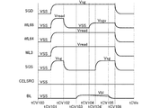
次に、図5に示す動作シーケンスの各ステップにおける動作波形について説明する。なお、以下で説明する動作波形は、図4に示すケース11を想定しており、特定データは、ワード線WL66に接続された1ビット/セルの特定メモリセルに記憶されるものとする。また、各ステップの動作波形は動作方式によって異なってくるためいくつかの代表的な動作方式を想定して説明する。
Next, operation waveforms in each step of the operation sequence shown in FIG. 5 will be described. Note that the operation waveforms described below are based on the
なお、図5中のステップS103は、ステップS104の処理中にバックグラウンドで処理されるか、ステップS102及びS104間で処理されるものであり、メモリセルのノードには現れない動作である。同様に、図5中のステップS105は、ステップS104の処理中にバックグラウンドで処理されるか、ステップS104及びS106間で処理されるものであり、メモリセルのノードには現れない動作である。したがって、これらステップの動作波形の説明は省略する。 Note that step S103 in FIG. 5 is performed in the background during the process of step S104 or between steps S102 and S104, and does not appear in the memory cell node. Similarly, step S105 in FIG. 5 is performed in the background during the process of step S104, or is performed between steps S104 and S106, and does not appear in the memory cell node. Therefore, description of the operation waveforms of these steps is omitted.
先ず、ステップS102について説明する。 First, step S102 will be described.
図6は、偶数番目のビット線と奇数番目のビット線とが同時にアクセスされるABL(All Bit Line)方式を用いた場合のステップS102の動作波形である。 FIG. 6 shows an operation waveform in step S102 when an ABL (All Bit Line) method in which even-numbered bit lines and odd-numbered bit lines are accessed simultaneously is used.
時刻tA100〜tA101の期間は、ステップS102開始時点の初期状態である。 The period from time tA100 to tA101 is the initial state at the start of step S102.
続いて、時刻tA101〜tA102の期間において、選択ゲート線SGS及びSGDを電圧Vsg(例えば、3.5V)まで昇圧する。また、ワード線WL2〜WL66を電圧Vread(例えば、6V)まで昇圧する。その結果、ビット線BLと共通ソース線CELSRCが電気的に接続され、メモリセルMCのチャネル電位が初期化される。但し、時刻tA101〜tA102の期間は、省略される場合もある。 Subsequently, during the period from time tA101 to tA102, the select gate lines SGS and SGD are boosted to a voltage Vsg (for example, 3.5 V). Further, the word lines WL2 to WL66 are boosted to a voltage Vread (for example, 6V). As a result, the bit line BL and the common source line CELSRC are electrically connected, and the channel potential of the memory cell MC is initialized. However, the period of time tA101 to tA102 may be omitted.
続いて、時刻tA102〜tA103の期間において、特定ワード線WL66を例えば電圧VSS(0V)まで放電させる。 Subsequently, in a period from time tA102 to tA103, the specific word line WL66 is discharged to, for example, the voltage VSS (0 V).
続いて、時刻tA103〜tA104の期間において、ビット線BLを電圧Vbl(例えば、0.5V)まで充電する。 Subsequently, the bit line BL is charged to a voltage Vbl (for example, 0.5 V) during a period from time tA103 to tA104.
続いて、時刻tA104〜tA105の期間において、特定ワード線WL66に特定データの読み出しに必要な電圧Vcg(例えば、0.5V)を印加する。その結果、特定メモリセルMC66に記憶された特定データに応じてビット線BLの電圧が変化する。この電圧の変化をページバッファ3のセンスアンプ回路SAで検知することで特定データを判別する。
Subsequently, during a period from time tA104 to tA105, a voltage Vcg (for example, 0.5 V) necessary for reading specific data is applied to the specific word line WL66. As a result, the voltage of the bit line BL changes according to the specific data stored in the specific memory cell MC66. Specific data is discriminated by detecting this change in voltage with the sense amplifier circuit SA of the
続いて、時刻tA105〜tA106の期間において、ビット線BLを例えば電圧VSS(0V)まで放電させる。 Subsequently, in the period of time tA105 to tA106, the bit line BL is discharged to, for example, the voltage VSS (0 V).
最後に、時刻tA106〜tAeの期間において、選択ゲート線SGD、SGS及びワード線WL3〜WL66の電圧を放電する。 Finally, the voltages of the selection gate lines SGD and SGS and the word lines WL3 to WL66 are discharged during the period of time tA106 to tAe.
以上が、ABL方式を用いた場合のステップS102となる。本実施形態の場合、時刻tA104〜tA105の期間において、特定ワード線WL66の電圧が、一般ワード線WL2〜WL65の電圧に比べて低いことに留意されたい。 The above is step S102 when the ABL method is used. In the present embodiment, it should be noted that the voltage of the specific word line WL66 is lower than the voltages of the general word lines WL2 to WL65 during the period of time tA104 to tA105.
なお、図6の場合、共通ソース線CELSRCを電圧VSS(0V)よりも高い電圧で充電する場合もある。また、メモリセルMCが形成されたウエルCPWELLの電圧を電圧VSS(0V)よりも高い電圧で充電する場合もある。この場合、概ねビット線BL、選択ゲート線SGS、SGD及びワード線WL2〜WL66の電圧もその分だけ高くなる。 In the case of FIG. 6, the common source line CELSRC may be charged with a voltage higher than the voltage VSS (0 V). In some cases, the voltage of the well CPWELL in which the memory cell MC is formed is charged with a voltage higher than the voltage VSS (0 V). In this case, the voltages of the bit line BL, the selection gate lines SGS, SGD, and the word lines WL2 to WL66 are also increased accordingly.
図7は、偶数番目のビット線と奇数番目のビット線とを交互にアクセスし、アクセスしない方のビット線をシールド線とするビット線シールド方式を用いた場合のステップS102の動作波形である。 FIG. 7 shows operation waveforms in step S102 when the bit line shield system is used in which even-numbered bit lines and odd-numbered bit lines are alternately accessed and the non-accessed bit line is a shield line.
時刻tA100〜tA102の期間については、図24に示す場合と同様であるため説明を省略する。 About the period of time tA100-tA102, since it is the same as that of the case shown in FIG. 24, description is abbreviate | omitted.
続いて、時刻tA102〜tA103の期間において、選択ゲート線SGS及び特定ワード線WL66を例えば電圧VSS(0V)まで放電させる。 Subsequently, in the period from time tA102 to tA103, the selection gate line SGS and the specific word line WL66 are discharged to, for example, the voltage VSS (0 V).
続いて、時刻tA103〜tA104において、ビット線BLを電圧Vbl(例えば、0.5V)まで充電する。 Subsequently, at time tA103 to tA104, the bit line BL is charged to a voltage Vbl (for example, 0.5 V).
続いて、時刻tA104〜tA104´の期間において、特定ワード線WL66に特定データの読み出しに必要な所定の電圧Vcg(例えば、0.5V)を印加する。 Subsequently, during a period from time tA104 to tA104 ′, a predetermined voltage Vcg (for example, 0.5 V) necessary for reading specific data is applied to the specific word line WL66.
続いて、時刻tA104´〜tA105の期間において、選択ゲート線SGSを電圧Vsg(例えば、0.5V)まで充電する。その結果、特定メモリセルMC66に記憶された特定データに応じてビット線BLの電圧が変化する。この電圧の変化をページバッファ3のセンスアンプ回路SAで検知することで特定データを判別する。
Subsequently, the select gate line SGS is charged to a voltage Vsg (for example, 0.5 V) during a period from time tA104 ′ to tA105. As a result, the voltage of the bit line BL changes according to the specific data stored in the specific memory cell MC66. Specific data is discriminated by detecting this change in voltage with the sense amplifier circuit SA of the
続く時刻tA105〜tAeの期間については、図6に示す場合と同様であるため説明を省略する。 The subsequent period of time tA105 to tAe is the same as that shown in FIG.
以上が、ビット線シールド方式を用いた場合のステップS102となる。本実施形態の場合、時刻tA104´〜tA105の期間において、特定ワード線WL66の電圧が、一般ワード線WL2〜WL65の電圧に比べて低いことに留意されたい。 The above is step S102 when the bit line shield system is used. It should be noted that in the present embodiment, the voltage of the specific word line WL66 is lower than the voltages of the general word lines WL2 to WL65 during the period of time tA104 ′ to tA105.
なお、図7に示す場合、共通ソース線CELSRCが電圧VSS(0V)よりも高い電圧で充電する場合もある。また、メモリセルMCが形成されたウエルCPWELLの電圧を電圧VSS(0V)よりも高い電圧で充電する場合もある。この場合、概ねビット線BL、選択ゲート線SGD、SGS及びワード線WL2〜WL66の電圧もその分だけ高くなる。 In the case shown in FIG. 7, the common source line CELSRC may be charged with a voltage higher than the voltage VSS (0 V). In some cases, the voltage of the well CPWELL in which the memory cell MC is formed is charged with a voltage higher than the voltage VSS (0 V). In this case, the voltages of the bit line BL, the selection gate lines SGD, SGS, and the word lines WL2 to WL66 are also increased accordingly.
次に、ステップS104について説明する。 Next, step S104 will be described.
ステップS104は、消去ベリファイリードステップBV→書き込みステップBP→消去ステップBE→消去ベリファイリードステップBV→書き込みステップBP2→消去ベリファイリードステップBV2→・・・(以降、消去ステップBE→消去ベリファイリードステップBV→書き込みステップBP2→消去ベリファイリードステップBV2の繰り返し)の各ステップで実現されている。 In step S104, erase verify read step BV → write step BP → erase step BE → erase verify read step BV → write step BP2 → erase verify read step BV2 →... (Hereinafter erase step BE → erase verify read step BV → This is realized in each step of writing step BP2 → erasure verify read step BV2.
図8は、ABL方式を用いた場合のステップS104の消去ベリファイステップBVの動作波形である。 FIG. 8 shows operation waveforms of the erase verify step BV in step S104 when the ABL method is used.
時刻tBV100〜tBV101の期間は、消去ベリファイステップBV開始時点の初期状態である。 The period from time tBV100 to tBV101 is an initial state at the start of the erase verify step BV.
続いて、時刻tBV101〜tBV102の期間において、選択ゲート線SDG及びSGSを電圧Vsg(例えば、3.5V)まで昇圧する。また、ワード線WL2〜WL66を電圧Vread(例えば、6V)まで昇圧する。その結果、ビット線BLと共通ソース線CELSRCが電気的に接続され、メモリセルMCのチャネル電位が初期化される。但し、時刻tBV101〜tBV102の期間は、省略される場合もある。更に、これと同時に、ビット線BL、共通ソース線CELSRC、メモリセルMCが形成されたウエルCPWELLの電圧を電圧Vsrce(例えば、1V)まで充電する。 Subsequently, during the period from time tBV101 to tBV102, the select gate lines SDG and SGS are boosted to a voltage Vsg (for example, 3.5 V). Further, the word lines WL2 to WL66 are boosted to a voltage Vread (for example, 6V). As a result, the bit line BL and the common source line CELSRC are electrically connected, and the channel potential of the memory cell MC is initialized. However, the period from time tBV101 to tBV102 may be omitted. At the same time, the voltage of the well CPWELL in which the bit line BL, the common source line CELSRC, and the memory cell MC are formed is charged to a voltage Vsrce (for example, 1 V).
続いて、時刻tBV102〜tBV103の期間において、ワード線WL2〜WL66を例えば電圧VSS(0V)まで放電させる。 Subsequently, during the period from time tBV102 to tBV103, the word lines WL2 to WL66 are discharged to, for example, the voltage VSS (0 V).
続いて、時刻tBV103〜tBV105の期間において、ビット線BLを電圧Vble(=Vsrce+Vbl=1.5V)まで充電する。その後、ビット線BLの電圧が変化する。この電圧の変化をページバッファ3のセンスアンプ回路SAで検知し、その結果、ビット線BLからの放電が検知されれば消去動作が完了したことになる。
Subsequently, the bit line BL is charged to the voltage Vble (= Vsrc + Vbl = 1.5 V) in the period from time tBV103 to tBV105. Thereafter, the voltage of the bit line BL changes. This change in voltage is detected by the sense amplifier circuit SA of the
続いて、時刻tBV105〜tBV106の期間において、ビット線BL、共通ソース線CELSRC及びウエルCPWELLを例えば電圧VSS(0V)まで放電させる。 Subsequently, in the period from time tBV105 to tBV106, the bit line BL, the common source line CELSRC, and the well CPWELL are discharged to, for example, the voltage VSS (0 V).
最後に、時刻tBV106〜tBVeの期間において、選択ゲート線SGS及びSGDを例えば電圧VSS(0V)まで放電させる。 Finally, in the period from time tBV106 to tBVe, the selection gate lines SGS and SGD are discharged to, for example, the voltage VSS (0 V).
以上が、ABL方式を用いた場合のステップS104の消去ベリファイリードステップBVとなる。本実施形態の場合、時刻tBV103〜tBV105の期間において、ワード線WL64及びWL66の電圧が、選択ゲート線SGS及びSGDの電圧に比べて低いことに留意されたい。 The above is the erase verify read step BV in step S104 when the ABL method is used. In the present embodiment, it should be noted that the voltages of the word lines WL64 and WL66 are lower than the voltages of the selection gate lines SGS and SGD in the period from time tBV103 to tBV105.
以上のステップS104の消去ベリファイリードステップBVによって、メモリセルMCの閾値が概ね−1Vよりも高いか低いかを検知することができる。 By the erase verify read step BV in the above step S104, it can be detected whether the threshold value of the memory cell MC is higher or lower than about −1V.
ABL方式を用いた場合のステップS104の消去ベリファイリードステップBVは、動作方式によっては、偶数番目のワード線WLeと奇数番目のワード線WLoについて別々に実行されることもある。 The erase verify read step BV in step S104 when the ABL method is used may be executed separately for even-numbered word lines WLe and odd-numbered word lines WLo depending on the operation method.
具体的には、図9に示すように、時刻tBV100〜tBV200の期間において、偶数番目のワード線WLeについての消去ベリファイを実行し、時刻tBV200〜tBVeの期間において、奇数番目のワード線WLoについての消去ベリファイを実行する。 Specifically, as shown in FIG. 9, erase verify for the even-numbered word line WLe is executed in the period of time tBV100 to tBV200, and for the odd-numbered word line WLo in the period of time tBV200 to tBVe. Perform erase verify.
ここで、図9に示す時刻tBV100〜tBV200の期間は、奇数番目のワード線WLoの動作波形を除き、図8に示す時刻tBV100〜tBVeの期間と同じである。図9の場合、ワード線WLoは、時刻tBV102〜tBV106の期間において電圧Vread(例えば、6V)が維持され、時刻tBV106〜tBV200の期間において例えば電圧VSS(0V)まで放電される。 Here, the period of time tBV100 to tBV200 shown in FIG. 9 is the same as the period of time tBV100 to tBVe shown in FIG. 8 except for the operation waveform of the odd-numbered word line WLo. In the case of FIG. 9, the word line WLo is maintained at the voltage Vread (for example, 6 V) during the period from time tBV102 to tBV106, and is discharged to, for example, the voltage VSS (0 V) during the period from time tBV106 to tBV200.
また、図9に示す時刻tBV200〜tBVeの期間は、偶数番目のワード線WLeの動作波形を除き、図8に示す時刻tBV100〜tBVeの期間と同じである。図9の場合、ワード線WLeは、時刻tBV202〜tBV206の期間において電圧Vread(例えば、6V)が維持され、時刻tBV206〜tBVeの期間において例えば電圧VSS(0V)まで放電される。 Further, the period of time tBV200 to tBVe shown in FIG. 9 is the same as the period of time tBV100 to tBVe shown in FIG. 8 except for the operation waveform of the even-numbered word line WLe. In the case of FIG. 9, the word line WLe is maintained at the voltage Vread (for example, 6 V) in the period from the time tBV202 to tBV206, and is discharged to, for example, the voltage VSS (0 V) in the period from the time tBV206 to tBVe.
以上が、ABL方式を用いた場合であって、偶数番目のワード線WLeと奇数番目のワード線WLoについて別々に実行される場合のステップS104の消去ベリファイリードステップBVとなる。 The above is the case where the ABL method is used, and is the erase verify read step BV in step S104 when the even-numbered word line WLe and the odd-numbered word line WLo are separately executed.
図10は、ビット線シールド方式を用いた場合のステップS104の消去ベリファイステップBVの動作波形である。 FIG. 10 shows operation waveforms of the erase verify step BV in step S104 when the bit line shield method is used.
時刻tBV100〜tBV101の期間は、消去ベリファイステップBV開始時点の初期状態である。 The period from time tBV100 to tBV101 is an initial state at the start of the erase verify step BV.
続いて、時刻tBV101〜tBV102の期間において、選択ゲート線SGSを電圧Vsg(例えば、3.5V)まで昇圧する。また、共通ソース線CELSRCを電圧VDD(例えば、2.5V)まで充電する。 Subsequently, in the period from time tBV101 to tBV102, the selection gate line SGS is boosted to a voltage Vsg (for example, 3.5 V). Further, the common source line CELSRC is charged to a voltage VDD (for example, 2.5 V).
続いて、時刻tBV102〜tBV103の期間において、ワード線WL2〜WL66を電圧Vcge(例えば、0.5V)まで昇圧する。 Subsequently, during the period of time tBV102 to tBV103, the word lines WL2 to WL66 are boosted to a voltage Vcge (for example, 0.5 V).
続いて、時刻tBV103〜tBV105の期間において、選択ゲート線SGDを電圧Vsg(例えば、3.5V)まで昇圧する。その結果、偶数番目のビット線BLeの電圧が変化する。このビット線BLeの電圧Vblが高くなればビット線BLeについてのメモリセルMCeの消去動作が完了したことになる。 Subsequently, in the period from time tBV103 to tBV105, the selection gate line SGD is boosted to a voltage Vsg (for example, 3.5 V). As a result, the voltage of the even-numbered bit line BLe changes. If the voltage Vbl of the bit line BLe increases, the erase operation of the memory cell MCe for the bit line BLe is completed.
続いて、時刻tBV105〜tBV106の期間において、ビット線BL及び共通ソース線CELSRCを例えば電圧VSS(0V)まで放電させる。 Subsequently, in the period from time tBV105 to tBV106, the bit line BL and the common source line CELSRC are discharged to, for example, the voltage VSS (0 V).
続いて、時刻tBV106〜tBV200において、選択ゲート線SGS、SGD及びワード線WL2〜WL66を例えば電圧VSS(0V)まで放電させる。 Subsequently, at time tBV106 to tBV200, the select gate lines SGS and SGD and the word lines WL2 to WL66 are discharged to, for example, the voltage VSS (0 V).
続く時刻tBV200〜tBVeの期間は、奇数番目のビット線BLoについて時刻tBV100〜tBV200の期間と同様の動作を実行する。 In the subsequent period from time tBV200 to tBVe, the same operation as in the period from time tBV100 to tBV200 is performed on the odd-numbered bit line BLo.
以上が、ビット線シールド方式を用いた場合のステップS104の消去ベリファイリードステップBVとなる。本実施形態の場合、時刻tBV103〜tBV105及びtBV203〜tBV205の期間において、ワード線WL64及びWL66の電圧が、選択ゲート線SGS及びSGDの電圧に比べて低いことと、ウエルCPWELLの電圧が0Vであることに留意されたい。 The above is the erase verify read step BV of step S104 when the bit line shield method is used. In the case of the present embodiment, the voltages of the word lines WL64 and WL66 are lower than the voltages of the selection gate lines SGS and SGD and the voltage of the well CPWELL is 0 V in the period of time tBV103 to tBV105 and tBV203 to tBV205. Please note that.
以上のステップS104の消去ベリファイリードステップBVによって、メモリセルMCに流れるセル電流にも依るが、メモリセルMCの閾値が概ね−0.5V〜−1.5V程度よりも高いか低いかを検知することができる。 The erase verify read step BV in step S104 detects whether the threshold value of the memory cell MC is higher or lower than about −0.5V to −1.5V, depending on the cell current flowing through the memory cell MC. be able to.
ビット線シールド方式を用いた場合のステップS104の消去ベリファイステップBVは、動作方式によっては、偶数番目のワード線WLeと奇数番目のワード線WLoについて別々に実行されることもある。 The erase verify step BV in step S104 when the bit line shield method is used may be executed separately for even-numbered word lines WLe and odd-numbered word lines WLo depending on the operation method.
具体的には、図11に示すように、時刻tBV100〜tBV300の期間において、偶数番目のワード線WLeについての消去ベリファイを実行し、時刻tBV300〜tBVeの期間において、奇数番目のワード線WLoについての消去ベリファイを実行する。 Specifically, as shown in FIG. 11, erase verify is performed for even-numbered word lines WLe in the period from time tBV100 to tBV300, and for odd-numbered word lines WLo in the period from time tBV300 to tBVe. Perform erase verify.
ここで、図11に示す時刻tBV100〜tBV300の期間は、奇数番目のワード線WLoの動作波形を除き、図10に示す時刻tBV100〜tBVeの期間と同じである。図11の場合、ワード線WLoは、時刻tBV102〜tBV105及びtBV202〜tBV205の期間において電圧Vread(例えば、6V)まで昇圧される。 Here, the period from time tBV100 to tBV300 shown in FIG. 11 is the same as the period from time tBV100 to tBVe shown in FIG. 10 except for the operation waveform of the odd-numbered word line WLo. In the case of FIG. 11, the word line WLo is boosted to a voltage Vread (for example, 6 V) in the period of time tBV102 to tBV105 and tBV202 to tBV205.
また、図11に示す時刻tBV300〜tBVeの期間は、偶数番目のワード線WLeの動作波形を除き、図10に示す時刻tBV100〜tBVeの期間と同じである。図11の場合、ワード線WLeは、時刻tBV302〜tBV305及びtBV402〜tBV405の期間において電圧Vread(例えば、6V)まで昇圧される。 Further, the period of time tBV300 to tBVe shown in FIG. 11 is the same as the period of time tBV100 to tBVe shown in FIG. 10 except for the operation waveform of the even-numbered word line WLe. In the case of FIG. 11, the word line WLe is boosted to a voltage Vread (for example, 6 V) in the period of time tBV302 to tBV305 and tBV402 to tBV405.
以上が、ビット線シールド方式を用いた場合であって、偶数番目のワード線WLeと奇数番目のワード線WLoとについて別々に実行される場合のステップS104の消去ベリファイリードステップBVとなる。 The above is the case where the bit line shield system is used, and is the erase verify read step BV in step S104 when the even-numbered word line WLe and the odd-numbered word line WLo are separately executed.
ステップS104の消去ベリファイステップBV2は、電圧Vsrce又はVcgeが図8〜図11に示す場合よりも高いことを除き、ステップS104の消去ベリファイステップBVと同じである。 The erase verify step BV2 in step S104 is the same as the erase verify step BV in step S104 except that the voltage Vsrc or Vcge is higher than that shown in FIGS.
後述のステップS104の書き込みステップBP2では、消去されたメモリセルMCに対する過消去を防止するため、この消去されたメモリセルMCを少し書き戻す操作をする。そのため、消去ベリファイステップBV2では、そのベリファイリードとして、消去ベリファイの判定閾値電圧(Vsrce又はVcge)と同じか又はやや高い閾値電圧でベリファイリードする。そして、判定閾値電圧を越えたメモリセルMCが所定の個数を越えた場合に書き込みステップBP2の書き込み(書き戻し)ベリファイリードを完了させる。 In a write step BP2 in step S104, which will be described later, in order to prevent over-erasure of the erased memory cell MC, an operation of writing back the erased memory cell MC is performed a little. Therefore, in the erase verify step BV2, as the verify read, the verify read is performed at a threshold voltage that is the same as or slightly higher than the determination threshold voltage (Vsrc or Vcge) of the erase verify. Then, when the number of memory cells MC exceeding the determination threshold voltage exceeds a predetermined number, the write (write-back) verify read in the write step BP2 is completed.
次に、ステップS104の書き込みステップBPの前提として、書き込みステップBP2について説明する。 Next, the write step BP2 will be described as a premise of the write step BP in step S104.
図12は、ブロック内の全てのワード線について一斉に書き込みをする場合のステップS104の書き込みステップBP2の動作波形である。 FIG. 12 is an operation waveform of the write step BP2 in step S104 when writing is performed simultaneously for all the word lines in the block.
時刻tBP100〜tBP101の期間は、書き込みステップBP2開始時点の初期状態である。 The period from time tBP100 to tBP101 is the initial state at the start of the writing step BP2.
続いて、時刻tBP101〜tBP102の期間において、共通ソース線CELSRC、選択ゲート線SGS及びSGDをそれぞれ電圧Vsrc(例えば、2V)、Vsgs(例えば、1.5V)、Vsgd(例えば、2.5V)まで充電する。 Subsequently, in the period from time tBP101 to time tBP102, the common source line CELSRC and the selection gate lines SGS and SGD are set to voltages Vsrc (for example, 2 V), Vsgs (for example, 1.5 V), and Vsgd (for example, 2.5 V), respectively. Charge.
続いて、時刻tBP102〜tBP103の期間において、ワード線WL2〜WL66を電圧Vpass(例えば、8V)まで充電する。 Subsequently, during the period from time tBP102 to tBP103, the word lines WL2 to WL66 are charged to a voltage Vpass (for example, 8V).
続いて、時刻tBP103〜tBP104の期間において、ワード線WL2〜WL66をデータの書き込みに必要な電圧Vspgm(例えば、13V程度)まで充電する。また、書き込みしないビット線BLを電源電圧VDD(例えば、2.5V)、書き込みするビット線BLを例えば電圧VSS(0V)まで充電する。 Subsequently, during a period from time tBP103 to time tBP104, the word lines WL2 to WL66 are charged to a voltage Vspgm (for example, about 13 V) necessary for data writing. Further, the non-written bit line BL is charged to the power supply voltage VDD (for example, 2.5 V), and the written bit line BL is charged to the voltage VSS (0 V), for example.
続いて、時刻tBP104〜tBP105の期間において、ワード線WL2〜WL66を電圧Vpass(例えば、8V)まで放電させる。 Subsequently, in the period of time tBP104 to tBP105, the word lines WL2 to WL66 are discharged to a voltage Vpass (for example, 8V).
続いて、時刻tBP105〜tBP106の期間において、ビット線BLを例えば電圧VSS(0V)まで放電させる。 Subsequently, during the period from time tBP105 to tBP106, the bit line BL is discharged to, for example, the voltage VSS (0 V).
続いて、時刻tBP106〜tBP107の期間において、ワード線WL2〜WL66を例えば電圧VSS(0V)まで放電させる。 Subsequently, during the period from time tBP106 to time tBP107, the word lines WL2 to WL66 are discharged to, for example, the voltage VSS (0 V).
最後に、時刻tBP107〜tBPeの期間において、共通ソース線CELSRC、選択ゲート線SGD及びSGSを例えば電圧VSS(0V)まで放電させる。 Finally, in the period from time tBP107 to tBPe, the common source line CELSRC and the selection gate lines SGD and SGS are discharged to, for example, the voltage VSS (0 V).
以上が、ブロック内の全てのワード線について一斉に書き込みをする場合のステップS104の書き込みステップBP2となる。本実施形態の場合、全てのワード線WL2〜WL66が、時刻tBP103〜tBP104の期間において、最も高い電圧(例えば、13V程度)になっていることに留意されたい。 The above is the write step BP2 in step S104 when writing is performed for all the word lines in the block at the same time. It should be noted that in the present embodiment, all the word lines WL2 to WL66 are at the highest voltage (for example, about 13 V) during the period from time tBP103 to tBP104.
なお、図12に示す場合、時刻tBP100〜tBP101の期間において別の充放電が追加される場合もある。また、ウエルCPWELLの電圧は0Vである。 In addition, in the case shown in FIG. 12, another charge / discharge may be added in the period of time tBP100-tBP101. The voltage of the well CPWELL is 0V.
ステップS104の書き込みステップBPは、消去ステップBE前に実行されるステップであり、消去状態にあるメモリセルMCに対して書き込みを行い、等がメモリセルMCの閾値を書き込み状態のメモリセルMCと同程度まで高くするための動作である。 The write step BP of step S104 is a step that is executed before the erase step BE, and writes to the memory cell MC that is in the erased state. This is an operation for raising the level to the extent.
この書き込みステップBPは、電圧Vspgm(例えば、20V)が高い点を除き、ステップS104の書き込みステップBPと同じである。 This write step BP is the same as the write step BP in step S104 except that the voltage Vspgm (for example, 20 V) is high.
図13は、ステップS104の消去ステップBEの動作波形である。ここで、信号線SGSIN、SGDIN及びCG2〜CG66は、それぞれ選択ゲート線SGS、SGD及びワード線WL2〜WL66にロウデコーダ2aの転送トランジスタを介して接続されており、それぞれ選択ゲート線SGS、SGD及びワード線WL2〜WL66を検知することができる信号線である。
FIG. 13 shows operation waveforms of the erasing step BE in step S104. Here, the signal lines SGSIN, SGDIN, and CG2 to CG66 are respectively connected to the selection gate lines SGS and SGD and the word lines WL2 to WL66 via the transfer transistors of the
時刻tBE100〜tBE101は、消去ステップBE開始時点の初期状態である。 Times tBE100 to tBE101 are initial states at the start of the erasing step BE.
続いて、時刻tBE101〜tBE102の期間において、選択ゲート線SGS、SGDを電源電圧VDD(例えば、2.5V程度)まで充電する共に、ワード線WL2〜WL66を電圧Viso(0.5V程度)まで初期充電する。その際、選択ゲート線SGS、SGD及びワード線WL2〜WL66は、ロウデコーダ2aの転送トランジスタの閾値落ちする電圧まで充電された後、転送トランジスタがカットオフすることによってフローティング状態になる。
Subsequently, in the period from time tBE101 to tBE102, the selection gate lines SGS and SGD are charged to the power supply voltage VDD (for example, about 2.5V), and the word lines WL2 to WL66 are initially set to the voltage Viso (about 0.5V). Charge. At this time, the selection gate lines SGS and SGD and the word lines WL2 to WL66 are charged to a voltage at which the threshold value of the transfer transistor of the
続いて、時刻tBE102〜tBE106の期間において、ウエルCPWELLの電圧を消去に必要な電圧Vera(例えば、20V)まで昇圧する。その結果、容量結合によって、図中破線に示すように、フローティング状態の選択ゲート線SGS、SGD及びワード線WL2〜WL66が電圧Vera近傍まで昇圧される。また、メモリセルMC内の拡散層接合の順方向バイアスによって、図中破線に示すように、ビット線BL及び共通ソース線CELSRCも電圧Vera近傍まで昇圧される。 Subsequently, in the period from time tBE102 to tBE106, the voltage of the well CPWELL is boosted to a voltage Vera (for example, 20 V) necessary for erasing. As a result, as shown by the broken lines in the figure, the floating selection gate lines SGS and SGD and the word lines WL2 to WL66 are boosted to the vicinity of the voltage Vera by capacitive coupling. Further, the bit line BL and the common source line CELSRC are boosted to the vicinity of the voltage Vera as shown by the broken line in the drawing by the forward bias of the diffusion layer junction in the memory cell MC.
続いて、時刻tBE106〜tBE107の期間において、ウエルCPWELLを0Vまで放電させる。その結果、ビット線BL、共通ソース線CELSRC、選択ゲート線SGS、SGD及びワード線WL2〜WL66が、時刻tBE102における電圧の近傍まで降圧される。 Subsequently, the well CPWELL is discharged to 0 V in the period from time tBE106 to time tBE107. As a result, the bit line BL, the common source line CELSRC, the select gate lines SGS, SGD, and the word lines WL2 to WL66 are stepped down to the vicinity of the voltage at time tBE102.
最後に、時刻tBE107〜tBEeの期間において、信号線SGSIN、SGDIN及びCG2〜CG66を例えば電圧VSS(0V)まで放電させる。その結果、ロウデコーダ2aの転送トランジスタを介して選択ゲート線SGS、SGD及びワード線WL2〜WL66も0Vまで放電される。
Finally, in the period of time tBE107 to tBEe, the signal lines SGSIN, SGDIN and CG2 to CG66 are discharged to, for example, the voltage VSS (0 V). As a result, the select gate lines SGS and SGD and the word lines WL2 to WL66 are also discharged to 0 V through the transfer transistor of the
以上が、ステップS104の消去ステップBEとなる。本実施形態の場合、時刻tBE102〜tBE106の期間において、ウエルCPWELLの電圧が電圧Vera(例えば、15V〜20V程度)に昇圧されることに留意されたい。 The above is the erasing step BE in step S104. It should be noted that in the present embodiment, the voltage of the well CPWELL is boosted to the voltage Vera (for example, about 15V to 20V) during the period of time tBE102 to tBE106.
次に、ステップS106について説明する。 Next, step S106 will be described.
ステップS106は、書き込みベリファイリードステップCV→書き込みステップCP→書き込みベリファイリードステップCV→・・・(以降、書き込みステップCP→書き込みベリファイリードステップCVの繰り返し)の各ステップで実現されている。なお、ステップS106の最初と最後のステップは、書き込みステップCP及び書き込みベリファイリードステップCVのいずれの場合も有り得る。 Step S106 is realized in each step of write verify read step CV → write step CP → write verify read step CV →... (Hereinafter, write step CP → write verify read step CV is repeated). Note that the first and last steps of step S106 can be either the write step CP or the write verify read step CV.
図14は、ステップS106の書き込みステップCPの動作波形である。 FIG. 14 shows operation waveforms in the write step CP in step S106.
時刻tCP100〜tCP101は、書き込みステップCP開始時点の初期状態である。 Times tCP100 to tCP101 are initial states at the start of the writing step CP.
続いて、時刻tCP101〜tCP102の期間において、共通ソース線CELSRC、選択ゲートSGS及びSGDをそれぞれ電圧Vsrc(例えば、2V)、Vsgs(例えば、1.5V)、Vsgd(例えば、2.5V)まで充電する。 Subsequently, in the period from time tCP101 to tCP102, the common source line CELSRC and the selection gates SGS and SGD are charged to voltages Vsrc (for example, 2 V), Vsgs (for example, 1.5 V), and Vsgd (for example, 2.5 V), respectively. To do.
続いて、時刻tCP102〜tCP103の期間において、ワード線WL2〜WL66を電圧Vpass(例えば、8V)まで充電する。 Subsequently, during the period from time tCP102 to tCP103, the word lines WL2 to WL66 are charged to a voltage Vpass (for example, 8V).
続いて、時刻tCP103〜tCP104の期間において、特定ワード線WL66を特定データの書き込みに必要な電圧Vpgm(例えば、20V程度)まで充電する。また、書き込みしないビット線BLを電源電圧VDD(例えば、2.5V)、書き込みするビット線BLを例えば電圧VSS(0V)まで充電する。 Subsequently, in a period from time tCP103 to tCP104, the specific word line WL66 is charged to a voltage Vpgm (for example, about 20 V) necessary for writing specific data. Further, the non-written bit line BL is charged to the power supply voltage VDD (for example, 2.5 V), and the written bit line BL is charged to the voltage VSS (0 V), for example.
続いて、時刻tCP104〜tCP105の期間において、特定ワード線WL66を電圧Vpass(例えば、8V)まで放電させる。 Subsequently, in a period from time tCP104 to tCP105, the specific word line WL66 is discharged to a voltage Vpass (for example, 8V).
続いて、時刻tCP105〜tCP106の期間において、ビット線BLを例えば電圧VSS(0V)まで放電させる。 Subsequently, in the period of time tCP105 to tCP106, the bit line BL is discharged to, for example, the voltage VSS (0 V).
続いて、時刻tCP106〜tCP107の期間において、ワード線WL2〜WL66を例えば電圧VSS(0V)まで放電させる。 Subsequently, in the period from time tCP106 to time tCP107, the word lines WL2 to WL66 are discharged to, for example, the voltage VSS (0 V).
最後に、時刻tCP107〜tCPeの期間において、共通ソース線CELSRC、選択ゲート線SGS及びSGDを例えば電圧VSS(0V)まで放電させる。 Finally, in the period of time tCP107 to tCPe, the common source line CELSRC and the selection gate lines SGS and SGD are discharged to, for example, the voltage VSS (0 V).
以上が、ステップS106の書き込みステップCEとなる。本実施形態の場合、時刻tCP103〜tCP104において、特定ワード線WL66の電圧が一般ワード線WL2〜WL65よりも高い電圧であることに留意されたい。 The above is the writing step CE in step S106. Note that in the present embodiment, the voltage of the specific word line WL66 is higher than that of the general word lines WL2 to WL65 at times tCP103 to tCP104.
なお、図14に示す場合、時刻tCP100〜tCP101の期間において別の充放電が追加される場合もある。また、ウエルCPWELLの電圧は0Vである。 In the case shown in FIG. 14, another charge / discharge may be added in the period from time tCP100 to tCP101. The voltage of the well CPWELL is 0V.
図15は、ABL方式を用いた場合のステップS106の書き込みベリファイリードステップCVの動作波形である。 FIG. 15 shows operation waveforms of the write verify read step CV in step S106 when the ABL method is used.
時刻tCV100〜tCV101の期間は、ステップS106の書き込みベリファイリードステップCV開始時点の初期状態である。 The period from time tCV100 to tCV101 is the initial state at the start of the write verify read step CV in step S106.
続いて、時刻tCV101〜tCV102の期間において、選択ゲート線SGS及びSGDを電圧Vsg(例えば、3.5V)まで昇圧する。また、ワード線WL2〜WL66を電圧Vread(例えば、6V)まで昇圧する。その結果、ビット線BLと共通ソース線CELSRCが電気的に接続され、メモリセルMCのチャネル電位が初期化される。但し、時刻tCV101〜tCV102の期間は、省略される場合もある。 Subsequently, during the period from time tCV101 to tCV102, the select gate lines SGS and SGD are boosted to a voltage Vsg (for example, 3.5 V). Further, the word lines WL2 to WL66 are boosted to a voltage Vread (for example, 6V). As a result, the bit line BL and the common source line CELSRC are electrically connected, and the channel potential of the memory cell MC is initialized. However, the period from time tCV101 to tCV102 may be omitted.
続いて、時刻tCV102〜tCV103の期間において、特定ワード線WL66を例えば電圧VSS(0V)まで放電させる。 Subsequently, in a period from time tCV102 to tCV103, the specific word line WL66 is discharged to, for example, the voltage VSS (0 V).
続いて、時刻tCV103〜tCV104の期間において、ビット線BLを電圧Vbl(例えば、0.5V)まで充電する。 Subsequently, in the period from time tCV103 to tCV104, the bit line BL is charged to a voltage Vbl (for example, 0.5 V).
続いて、時刻tCV104〜tCV105の期間において、特定ワード線WL66に特定データの読み出しに必要な電圧Vcgv(例えば、0.5V)を印加する。その後、ビット線BLの電圧が変化する。この電圧の変化をページバッファ3のセンスアンプ回路SAで検知し、その結果、ビット線BLからの放電が検知されれば書き込み動作が完了したことになる。
Subsequently, during a period from time tCV104 to tCV105, a voltage Vcgv (for example, 0.5 V) necessary for reading specific data is applied to the specific word line WL66. Thereafter, the voltage of the bit line BL changes. This change in voltage is detected by the sense amplifier circuit SA of the
続いて、時刻tCV105〜tCV106の期間において、ビット線BLを例えば電圧VSS(0V)まで放電させる。 Subsequently, in the period of time tCV105 to tCV106, the bit line BL is discharged to, for example, the voltage VSS (0 V).
最後に、時刻tCV106〜tCVeの期間において、選択ゲート線SGD、SGS及びワード線WL3〜WL66を例えば電圧VSS(0V)まで放電させる。 Finally, in the period of time tCV106 to tCVe, the selection gate lines SGD and SGS and the word lines WL3 to WL66 are discharged to, for example, the voltage VSS (0 V).
以上が、ABL方式を用いた場合のステップS106の書き込みベリファイリードCVとなる。本実施形態の場合、時刻tCV104〜tCV105の期間において、特定ワード線WL66の電圧が、一般ワード線WL2〜WL65の電圧に比べて低いことに留意されたい。 The above is the write verify read CV in step S106 when the ABL method is used. It should be noted that in the present embodiment, the voltage of the specific word line WL66 is lower than the voltages of the general word lines WL2 to WL65 during the period of time tCV104 to tCV105.
なお、図15の場合、共通ソース線CELSRCを電圧VSS(0V)よりも高い電圧で充電する場合もある。また、メモリセルMCが形成されたウエルCPWELLの電圧を電圧VSS(0V)よりも高い電圧で充電する場合もある。この場合、概ねビット線BL、選択ゲート線SGS、SGD及びワード線WL2〜WL66の電圧もその分だけ高くなる。 In the case of FIG. 15, the common source line CELSRC may be charged with a voltage higher than the voltage VSS (0 V). In some cases, the voltage of the well CPWELL in which the memory cell MC is formed is charged with a voltage higher than the voltage VSS (0 V). In this case, the voltages of the bit line BL, the selection gate lines SGS, SGD, and the word lines WL2 to WL66 are also increased accordingly.
図16は、ビット線シールド方式を用いた場合のステップS106の書き込みベリファイリードステップCVの動作波形である。 FIG. 16 shows an operation waveform of the write verify read step CV in step S106 when the bit line shield method is used.
時刻tCV100〜tCV102の期間については、図15に示す場合と同様であるため説明を省略する。 About the period of time tCV100-tCV102, since it is the same as that of the case shown in FIG. 15, description is abbreviate | omitted.
続いて、時刻tCV102〜tCV103の期間において、選択ゲート線SGS及び特定ワード線WL66を例えば電圧VSS(0V)まで放電させる。 Subsequently, in the period from time tCV102 to tCV103, the selection gate line SGS and the specific word line WL66 are discharged to, for example, the voltage VSS (0 V).
続いて、時刻tCV103〜tCV104において、ビット線BLを電圧Vbl(例えば、0.5V)まで充電する。 Subsequently, at time tCV103 to tCV104, the bit line BL is charged to a voltage Vbl (for example, 0.5 V).
続いて、時刻tCV104〜tCV104´の期間において、特定ワード線WL66に特定データの読み出しに必要な電圧Vcgv(例えば、0.5V)を印加する。 Subsequently, during the period from time tCV104 to tCV104 ′, a voltage Vcgv (for example, 0.5 V) necessary for reading specific data is applied to the specific word line WL66.
続いて、時刻tCV104´〜tCV105の期間において、選択ゲート線SGSを電圧Vsg(例えば、0.5V)まで充電する。その後、ビット線BLの電圧が変化する。この電圧の変化をページバッファ3のセンスアンプ回路SAで検知し、その結果、ビット線BLからの放電が検知されれば書き込み動作が完了したことになる。
Subsequently, in the period from time tCV104 ′ to tCV105, the selection gate line SGS is charged to a voltage Vsg (for example, 0.5 V). Thereafter, the voltage of the bit line BL changes. This change in voltage is detected by the sense amplifier circuit SA of the
続く時刻tCV105〜tCVeの期間については、図33に示す場合と同様であるため説明を省略する。 The subsequent period of time tCV105 to tCVe is the same as that shown in FIG.
以上が、ビット線シールド方式を用いた場合のステップS106の書き込みベリファイリードステップCVとなる。本実施形態の場合、時刻tCV104´〜tCV105の期間において、特定ワード線WL66の電圧が、一般ワード線WL2〜WL65の電圧に比べて低いことに留意されたい。 The above is the write verify read step CV of step S106 when the bit line shield method is used. In the present embodiment, it should be noted that the voltage of the specific word line WL66 is lower than the voltages of the general word lines WL2 to WL65 during the period of time tCV104 ′ to tCV105.
なお、図16に示す場合、共通ソース線CELSRCが電圧VSS(0V)よりも高い電圧で充電する場合もある。また、メモリセルMCが形成されたウエルCPWELLの電圧を電圧VSS(0V)よりも高い電圧で充電する場合もある。この場合、概ねビット線BL、選択ゲート線SGD、SGS及びワード線WL2〜WL66の電圧もその分だけ高くなる。 In the case shown in FIG. 16, the common source line CELSRC may be charged with a voltage higher than the voltage VSS (0 V). In some cases, the voltage of the well CPWELL in which the memory cell MC is formed is charged with a voltage higher than the voltage VSS (0 V). In this case, the voltages of the bit line BL, the selection gate lines SGD, SGS, and the word lines WL2 to WL66 are also increased accordingly.
<書き込み期間中のシーケンス>
ここでは、本実施形態に係る半導体記憶装置の書き込み期間中の動作シーケンスについて説明する。
<Sequence during writing period>
Here, an operation sequence during the writing period of the semiconductor memory device according to the present embodiment will be described.
ここで、書き込み期間とは、特定のブロックの特定のページに対してデータの書き込みを行う書き込み動作と、この書き込み動作のための周辺回路の準備や後処理とを含む期間をいう。この期間は、典型的には、書き込みビジー信号がアクティブの期間と考えられるが、必ずしもこの期間と一致しなくても良い。 Here, the writing period refers to a period including a writing operation for writing data to a specific page in a specific block, and preparation and post-processing of peripheral circuits for the writing operation. This period is typically considered as a period during which the write busy signal is active, but does not necessarily coincide with this period.
図17は、書き込み期間中の動作シーケンスを示す図である。図中斜線で示されたステップS201、S204及びS206は、従来の書き込み期間中の動作シーケンスに相当するものである。但し、これらステップS201、S204及びS206における動作は、従来の場合と必ずしも一致するものではない。 FIG. 17 is a diagram illustrating an operation sequence during the writing period. Steps S201, S204, and S206 indicated by diagonal lines in the drawing correspond to an operation sequence during a conventional writing period. However, the operations in steps S201, S204, and S206 do not always match those in the conventional case.
始めに、ステップS201では、コントローラ11を介して外部から書き込みするプレーン、ブロック及びページのアドレスとコマンドが入力される。このプレーン、ブロック及びページのアドレスは、I/Oバッファ9を介してロウアドレスレジスタ5a、カラムアドレスレジスタ5bに送信される。また、コマンドは、ロジック制御回路6を介してシーケンス制御回路7に送信される。
First, in step S201, an address and a command of a plane, a block, and a page to be written from the outside are input via the
続いて、ステップS202において、書き込み対象となるブロック(以下、「書き込みブロック」と呼ぶ)が記憶する特定データをページバッファ3に読み出す。
Subsequently, in step S <b> 202, specific data stored in a block to be written (hereinafter referred to as “write block”) is read out to the
続いて、ステップS203において、ページバッファ3に保持された特定データをシーケンス制御回路7などの周辺回路のレジスタにセットする。
In step S203, the specific data held in the
続いて、ステップS204において、周辺回路のレジスタにセットされた特定データを用いて回路動作パラメータを調整した上で、この調整後の回路動作パラメータに応じて周辺回路を動作させ書き込みブロックのページにデータを書き込む(書き込み動作)。 Subsequently, in step S204, the circuit operation parameter is adjusted using the specific data set in the peripheral circuit register, and the peripheral circuit is operated according to the adjusted circuit operation parameter, and the data is written to the page of the write block. Is written (write operation).
最後に、ステップS207において、周辺回路のレジスタに保持されている特定データを所定のデフォルト値にリセットし、書き込み期間を終了させる(ステップS208)。 Finally, in step S207, the specific data held in the peripheral circuit register is reset to a predetermined default value, and the writing period is ended (step S208).
以上のように、本実施形態では、ブロック毎に用意された特定データを用いて回路動作パラメータが調整されるため、ブロック毎に適切な書き込み動作を実現することができる。 As described above, in this embodiment, the circuit operation parameter is adjusted using the specific data prepared for each block, so that an appropriate write operation can be realized for each block.
<本実施形態のまとめ>
以上、本実施形態によれば、動作回路パラメータとは別に、ブロック毎の特定データを用いて消去動作或いは書き込み動作がなされるため、微細化が進んだ場合であっても信頼性ないしパフォーマンスの悪化が抑制された半導体記憶装置を提供することができる。また、特定データをメモリセルに記憶させるため、記憶可能な特定データを増やすことが容易であるばかりでなく、メモリセルが不揮発性の場合には、不慮の電源遮断に対する特定データ消滅のリスクを低減することができる。
<Summary of this embodiment>
As described above, according to the present embodiment, the erase operation or the write operation is performed using the specific data for each block separately from the operation circuit parameter, so that reliability or performance deterioration is caused even when miniaturization progresses. It is possible to provide a semiconductor memory device in which the above is suppressed. In addition, since the specific data is stored in the memory cell, it is easy not only to increase the specific data that can be stored, but also when the memory cell is nonvolatile, the risk of the specific data disappearing due to accidental power interruption is reduced. can do.
[第2の実施形態]
第2の実施形態に係る半導体記憶装置の特定データの書き込み及び読み出し方法を説明する。
[Second Embodiment]
A method for writing and reading specific data in the semiconductor memory device according to the second embodiment will be described.
特定データは、ブロックにおけるデータの書き込み動作、消去動作時の周辺回路の動作を適切にするものであり非常に高い信頼性が要求される。 The specific data is used to appropriately operate the peripheral circuit at the time of data writing operation and erasing operation in the block, and very high reliability is required.
したがって、セル間干渉による特定メモリセルの閾値変動を抑制するため、1ビット/セルで特定データを記憶することが望ましい。 Therefore, it is desirable to store the specific data at 1 bit / cell in order to suppress the threshold fluctuation of the specific memory cell due to inter-cell interference.
また、第2の実施形態では、より信頼性を向上させるため、図18に示すように、特定データを取り扱う。 In the second embodiment, specific data is handled as shown in FIG. 18 in order to improve reliability.
図18に示す場合、1ビットの特定データA、B、・・・をそれぞれN個(例えば、8個(1バイト))の特定メモリセルに書き込んでおく。そして、N個の特定メモリセルから特定データを読み出した後、カラムデコーダ2bで多数決を取り、特定データA、B、・・・を確定させる。
In the case shown in FIG. 18, 1-bit specific data A, B,... Are written in N (for example, 8 (1 byte)) specific memory cells. Then, after reading the specific data from the N specific memory cells, a majority decision is taken by the
以上、第2の実施形態によれば、第1の実施形態と同様の効果を有するばかりでなく、複数の特定メモリセルによって特定データを記憶しておくので、セル間干渉等によって一部の特定メモリセルの閾値が変動してしまった場合であっても、正常な特定データを読み出すことが可能である。 As described above, according to the second embodiment, not only has the same effect as that of the first embodiment, but also the specific data is stored in a plurality of specific memory cells. Even when the threshold value of the memory cell changes, normal specific data can be read out.
[第3の実施形態]
第3の実施形態は、セル間干渉による特定メモリセルの閾値変動を抑制する半導体記憶装置である。
[Third Embodiment]
The third embodiment is a semiconductor memory device that suppresses threshold fluctuation of a specific memory cell due to inter-cell interference.
本実施形態では、図19に示すように、特定ワード線WLに接続されたメモリセルのうち偶数番目のビット線BLe及び偶数番目のビット線BLoの一方のビット線(図19に示す場合、ビット線BLe)で選択されるメモリセルを特定メモリセルとして用い、他方のビット線(図19に示す場合、ビット線BLo)で選択されるメモリセルは例えば消去状態(Er)のダミーセルとして用いる。 In the present embodiment, as shown in FIG. 19, one bit line of the even-numbered bit line BLe and the even-numbered bit line BLo among the memory cells connected to the specific word line WL (in the case shown in FIG. The memory cell selected by the line BLe) is used as a specific memory cell, and the memory cell selected by the other bit line (in the case of FIG. 19, bit line BLo) is used as a dummy cell in the erased state (Er), for example.
1ビットの特定データA、B、・・・を、第1の実施形態と同様、それぞれN個(例えば、8個(1バイト))の特定メモリセルに書き込む場合、1ビットの特定データの記憶には、特定メモリセルとダミーセルとを合わせて合計2N個のメモリセルを要する。 When 1-bit specific data A, B,... Are written in N (for example, 8 (1 byte)) specific memory cells as in the first embodiment, 1-bit specific data is stored. Requires a total of 2N memory cells including a specific memory cell and a dummy cell.
特定データの読み出しについては、第2の実施形態と同様であるため説明を省略する。 Since the reading of the specific data is the same as that of the second embodiment, the description is omitted.
以上、第3の実施形態によれば、第1及び第2の実施形態と同様の効果を有するばかりでなく、特定メモリセル間のダミーセルが配置されているため、第2の実施形態に比べて、セル間干渉の影響が少なく信頼性の高い特定データの記憶が可能になる。 As described above, according to the third embodiment, not only has the same effects as those of the first and second embodiments, but also because the dummy cells between the specific memory cells are arranged, compared with the second embodiment. Thus, it is possible to store specific data with less influence of inter-cell interference and high reliability.
[第4の実施形態]
第4の実施形態も、第2の実施形態と同様、セル間干渉による特定メモリセルの閾値変動を抑制する半導体記憶装置である。本実施形態は、図22に示すケース24及びケース34のように、複数の特定ワード線が隣接して配置されている場合に適用することができる。
[Fourth Embodiment]
Similarly to the second embodiment, the fourth embodiment is a semiconductor memory device that suppresses threshold fluctuation of a specific memory cell due to inter-cell interference. This embodiment can be applied to a case where a plurality of specific word lines are arranged adjacent to each other as in case 24 and case 34 shown in FIG.
本実施形態では、ワード線方向に特定メモリセル及びダミーセルを交互に配置し、且つ、ビット線方向に特定メモリセルが隣接しないように配置する。 In this embodiment, specific memory cells and dummy cells are alternately arranged in the word line direction, and are arranged so that the specific memory cells are not adjacent to each other in the bit line direction.
図20の場合、2本の特定ワード線WL及びWL´が配置されており、このうち特定ワード線WLについては、偶数番目のビット線BLeで選択されるメモリセルを特定メモリセルとして用い、奇数番目のビット線BLoで選択されるメモリセルを消去状態(Er)のダミーセルとして用いている。他方、特定ワード線WL´については、奇数番目のビット線BLoで選択されるメモリセルを特定メモリセルとして用い、奇数番目のビット線BLeで選択されるメモリセルを消去状態(Er)のダミーセルとして用いている。 In the case of FIG. 20, two specific word lines WL and WL ′ are arranged. Among these, for the specific word line WL, a memory cell selected by the even-numbered bit line BLe is used as a specific memory cell, and an odd number. The memory cell selected by the th bit line BLo is used as a dummy cell in the erased state (Er). On the other hand, for the specific word line WL ′, the memory cell selected by the odd-numbered bit line BLo is used as the specific memory cell, and the memory cell selected by the odd-numbered bit line BLe is used as the dummy cell in the erased state (Er). Used.
特定データの読み出しについては、第2及び第3の実施形態と同様であるため説明を省略する。 Since the reading of the specific data is the same as in the second and third embodiments, the description thereof is omitted.
なお、特定データA、B、・・・をそれぞれN個(例えば、8個(1バイト))の特定メモリセルに書き込む場合、第3の実施形態と同様、1ビットの特定データの記憶には、特定メモリセルとダミーセルとを合わせて合計2N個のメモリセルを要する。 When writing specific data A, B,... Into N (for example, 8 (1 byte)) specific memory cells, as in the third embodiment, 1-bit specific data is stored. In total, 2N memory cells are required in total including the specific memory cells and the dummy cells.
以上、第4の実施形態によれば、第1及び第2の実施形態と同様の効果を得られるばかりでなく、ワード線方向及びビット線方向に隣接する特定メモリセル間のセル間干渉効果の増大を抑制しつつ、第3の実施形態よりも多くの特定データを扱うことができる。 As described above, according to the fourth embodiment, not only the same effects as in the first and second embodiments can be obtained, but also the inter-cell interference effect between specific memory cells adjacent in the word line direction and the bit line direction can be reduced. While suppressing the increase, more specific data can be handled than in the third embodiment.
[側壁転写プロセス]
ここでは、上記実施形態の説明でも触れた、本実施形態に係る半導体装置の製造にも用いることができる側壁転写プロセスについて補足する。
[Sidewall transfer process]
Here, it supplements about the side wall transcription | transfer process which can be used also for manufacture of the semiconductor device which concerns on this embodiment touched also by description of the said embodiment.
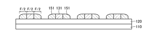
先ず、ライン幅F/2、スペース幅F/2のL/Sパターンの形成する場合の側壁転写プロセスについて図21〜図27を参照しながら説明する。ここで、Fはリソグラフィ技術の解像度による最小加工寸法を示している。 First, a sidewall transfer process in the case of forming an L / S pattern having a line width F / 2 and a space width F / 2 will be described with reference to FIGS. Here, F indicates the minimum processing dimension according to the resolution of the lithography technique.
始めに、図21に示すように、メモリセルや配線の材料からなる被加工膜110を形成した後、被加工膜110上にSiO2等からなる第1のマスク120及び第2のマスク130を順次積層する。更に、第2のマスク130の上面にスピンコート法などを用いてフォトレジスト140を塗布する。
First, as shown in FIG. 21, after a film to be processed 110 made of a memory cell or wiring material is formed, a
続いて、図22に示すように、フォトレジスト140にライン幅F、スペース幅FのL/Sパターンを露光する。
Subsequently, as shown in FIG. 22, the L / S pattern having a line width F and a space width F is exposed on the
続いて、図23に示すように、リソグラフィ技術を用いてフォトレジスト140のL/Sパターンを第2のマスク130に転写する。これによって、第2のマスク130にライン幅F、スペース幅FのL/Sパターンが形成される。
Subsequently, as shown in FIG. 23, the L / S pattern of the
続いて、図24に示すように、RIE(Reactive Ion Etching)法によるスリミング技術を用いて第2のマスク130のラインの両側面をF/4ずつ除去する。これによって、第2のマスク130にライン幅F/2、スペース幅(3/2)FのL/Sパターンが形成される。
Subsequently, as shown in FIG. 24, both sides of the line of the
続いて、図25に示すように、第2のマスク130のラインを芯材131として、その両側面にSiO2等からなる幅F/2の側壁151を形成する。
Subsequently, as shown in FIG. 25, the line of the
続いて、図26に示すように、例えばDHF(希フッ酸)を用いたウェットエッチングによって芯材131を除去する。これによって、ライン幅F/2、スペース幅F/2ののL/Sパターン150が形成される。
Subsequently, as shown in FIG. 26, the
続いて、図27に示すように、RIE法などの異方性エッチングを用いて第1のマスク120に、ライン幅F/2、スペース幅F/2のL/Sパターンを形成する。
Subsequently, as shown in FIG. 27, an L / S pattern having a line width F / 2 and a space width F / 2 is formed on the
その後、この第2のマスク120のL/Sパターンを用いたエッチングを施すことで、被加工膜110を最小加工寸法F/2で加工することができる。
Thereafter, by performing etching using the L / S pattern of the
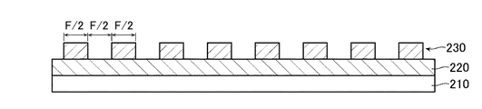
次に、ライン幅F/4、スペース幅F/4のL/Sパターンの形成する場合の側壁転写プロセスについて図28〜図38を参照しながら説明する。 Next, a sidewall transfer process in the case of forming an L / S pattern having a line width F / 4 and a space width F / 4 will be described with reference to FIGS.
始めに、図28に示すように、メモリセルや配線の材料からなる被加工膜210を形成した後、被加工膜210上にSiO2等からなる第1のマスク220、第2のマスク230及び第3のマスク240を順次積層する。更に、第3のマスク240の上面にスピンコート法などを用いてフォトレジスト250を塗布する。
First, as shown in FIG. 28, after a film to be processed 210 made of a memory cell or wiring material is formed, a
続いて、図29に示すように、フォトレジスト250にライン幅F、スペース幅FのL/Sパターンを露光する。
Subsequently, as shown in FIG. 29, an L / S pattern having a line width F and a space width F is exposed on the
続いて、図30に示すように、リソグラフィ技術を用いてフォトレジスト250のL/Sパターンを第3のマスク240に転写する。これによって、第3のマスク240にライン幅F、スペース幅FのL/Sパターンが形成される。
Subsequently, as illustrated in FIG. 30, the L / S pattern of the
続いて、図31に示すように、RIE法によるスリミング技術を用いて第3のマスク240のラインの両側面をF/4ずつ除去する。これによって、第3のマスク240にライン幅F/2、スペース幅(3/2)FのL/Sパターンが形成される。
Subsequently, as shown in FIG. 31, both sides of the line of the
続いて、図32に示すように、第3のマスク240のラインを芯材241として、その両側面にSiO2等からなる幅F/2の側壁261を形成する。
Subsequently, as shown in FIG. 32, a
続いて、図33に示すように、例えばDHFを用いたウェットエッチングによって芯材241を除去する。これによって、ライン幅F/2、スペース幅F/2のL/Sパターン260が形成される。
Subsequently, as shown in FIG. 33, the
続いて、図34に示すように、RIE法などの異方性エッチングを用いて第2のマスク230に、ライン幅F/2、スペース幅F/2のL/Sパターンを形成する。
Subsequently, as shown in FIG. 34, an L / S pattern having a line width F / 2 and a space width F / 2 is formed on the
続いて、図35に示すように、RIE法によるスリミング技術を用いて第2のマスク230のラインの両側面をF/8ずつ除去する。これよって、第2のマスク230にライン幅F/4、スペース幅(3/4)FのL/Sパターンが形成される。
Subsequently, as shown in FIG. 35, both sides of the line of the
続いて、図36に示すように、第2のマスク230のラインを芯材231として、その両側面にSiO2等からなる幅F/4の側壁271を形成する。
Subsequently, as shown in FIG. 36, the line of the
続いて、図37に示すように、例えばDHFを用いたウェットエッチングによって芯材231を除去する。これによって、ライン幅F/4、スペース幅F/4のL/Sパターン270が形成される。
Subsequently, as shown in FIG. 37, the
続いて、図38に示すように、RIE法などの異方性エッチングを用いて第1のマスク220に、ライン幅F/4、スペース幅F/4のL/Sパターンを形成する。
Subsequently, as shown in FIG. 38, an L / S pattern having a line width F / 4 and a space width F / 4 is formed on the
その後、この第1のマスク220のL/Sパターンを用いたエッチングを施すことで、被加工膜210を最小加工寸法F/4で加工することができる。
After that, by performing etching using the L / S pattern of the
以上、図21〜図27、図28〜図38を用いて説明したように、側壁転写プロセスを繰り返し行うことで、最小加工寸法を1/2ずつに微細化していくことが可能となる。 As described above with reference to FIG. 21 to FIG. 27 and FIG. 28 to FIG.
[その他]
以上、本発明のいくつかの実施形態を説明したが、これらの実施形態は、例として提示したものであり、発明の範囲を限定することは意図していない。これら新規な実施形態は、その他の様々な形態で実施されることが可能であり、発明の要旨を逸脱しない範囲で、種々の省略、置き換え、変更を行うことができる。これら実施形態やその変形は、発明の範囲や要旨に含まれるとともに、特許請求の範囲に記載された発明とその均等の範囲に含まれる。
[Others]
As mentioned above, although some embodiment of this invention was described, these embodiment is shown as an example and is not intending limiting the range of invention. These novel embodiments can be implemented in various other forms, and various omissions, replacements, and changes can be made without departing from the scope of the invention. These embodiments and modifications thereof are included in the scope and gist of the invention, and are included in the invention described in the claims and the equivalents thereof.
1・・・メモリセルアレイ、2a・・・ロウデコーダ/ワード線ドライバ、2b・・・カラムデコーダ、3・・・ページバッファ、4・・・NANDセルユニット、5a・・・ロウアドレスレジスタ、5b・・・カラムアドレスレジスタ、6・・・ロジック制御回路、7・・・シーケンス制御回路、8・・・高電圧発生回路、9・・・I/Oバッファ、10・・・NANDチップ、11・・・コントローラ、110、210・・・被加工膜、120、130、220、230、240・・・マスク、131、231、241・・・芯材、140、250・・・フォトレジスト、150、260、270・・・ラインアンドスペースパターン、151、261、271・・・側壁。
DESCRIPTION OF
Claims (6)
前記メモリセルアレイのメモリセルを消去する消去回路と
を備え、
前記メモリセルアレイは、複数のブロックに分割され、
前記各ブロックは、一部のワード線を特定ワード線として当該特定ワード線によりアクセスされるメモリセルの少なくとも一部又は全部が特定メモリセルに設定され、この特定メモリセルにユーザデータ以外の特定データを記憶し、
前記消去回路は、所定の前記ブロックに属するメモリセルの消去動作時に、当該ブロックに属する特定メモリセルに記憶された特定データを参照する
ことを特徴とする半導体記憶装置。 A memory cell array having a plurality of word lines and a plurality of bit lines, and a plurality of memory cells selected by the word lines and the bit lines;
An erasing circuit for erasing the memory cells of the memory cell array,
The memory cell array is divided into a plurality of blocks,
In each of the blocks, at least a part or all of memory cells accessed by the specific word line are set as specific memory cells by using some word lines as specific word lines, and specific data other than user data is set in the specific memory cells. Remember
The erasing circuit refers to specific data stored in a specific memory cell belonging to the block during an erasing operation of the memory cell belonging to the predetermined block.
ことを特徴とする請求項1記載の半導体記憶装置。 2. The semiconductor according to claim 1, wherein the specific data is written into the specific memory cell belonging to the predetermined block after the erasing operation in an erasing period including an erasing operation of the memory cell belonging to the predetermined block. Storage device.
ことを特徴とする請求項1又は2記載の半導体記憶装置。 The semiconductor memory device according to claim 1, wherein the specific data is read from the specific memory cell before the erase operation in an erase period including an erase operation of the memory cell.
ことを特徴とする請求項1〜3のいずれか1項記載の半導体記憶装置。 4. The memory cell array includes dummy word lines that are not used for storing the user data, in addition to word lines for selecting memory cells that store the user data. The semiconductor memory device described.
ことを特徴とする請求項4記載の半導体記憶装置。 The semiconductor memory device according to claim 4, wherein the specific word line also serves as the dummy word line.
所定の前記特定ワード線で選択される複数のメモリセルのうちの当該特定ワード線で選択される特定メモリセルに隣接するメモリセルは、データの記憶に用いないダミーセルであり、
前記メモリセルアレイは、隣接する2本の前記特定ワード線を有し、これら前記2本の特定ワード線のうち、一方の前記特定ワード線で選択される特定メモリセルと、他方の前記特定ワード線で選択される特定メモリセルとは隣接しておらず、
前記メモリセルアレイは、同一の前記特定データを複数の前記特定メモリセルに書き込み、
前記消去回路は、前記特定データの参照の際、前記同一の特定データを書き込んだ複数の特定メモリセルが記憶するデータの多数決を取る
ことを特徴とする請求項1〜5のいずれか1項記載の半導体記憶装置。 A part of the specific memory cell stores only the specific data,
Of the plurality of memory cells selected by the specific word line, the memory cell adjacent to the specific memory cell selected by the specific word line is a dummy cell that is not used for data storage.
The memory cell array has two adjacent specific word lines, and the specific memory cell selected by one specific word line of the two specific word lines and the other specific word line. Is not adjacent to the specific memory cell selected by
The memory cell array writes the same specific data to a plurality of the specific memory cells,
6. The erasing circuit takes a majority vote of data stored in a plurality of specific memory cells in which the same specific data is written when referring to the specific data. Semiconductor memory device.
Priority Applications (2)
| Application Number | Priority Date | Filing Date | Title |
|---|---|---|---|
| JP2011060596A JP2012198949A (en) | 2011-03-18 | 2011-03-18 | Semiconductor memory device |
| US13/418,955 US20120236644A1 (en) | 2011-03-18 | 2012-03-13 | Semiconductor storage device |
Applications Claiming Priority (1)
| Application Number | Priority Date | Filing Date | Title |
|---|---|---|---|
| JP2011060596A JP2012198949A (en) | 2011-03-18 | 2011-03-18 | Semiconductor memory device |
Publications (1)
| Publication Number | Publication Date |
|---|---|
| JP2012198949A true JP2012198949A (en) | 2012-10-18 |
Family
ID=46828340
Family Applications (1)
| Application Number | Title | Priority Date | Filing Date |
|---|---|---|---|
| JP2011060596A Withdrawn JP2012198949A (en) | 2011-03-18 | 2011-03-18 | Semiconductor memory device |
Country Status (2)
| Country | Link |
|---|---|
| US (1) | US20120236644A1 (en) |
| JP (1) | JP2012198949A (en) |
Cited By (1)
| Publication number | Priority date | Publication date | Assignee | Title |
|---|---|---|---|---|
| US9543027B2 (en) | 2013-09-13 | 2017-01-10 | Kabushiki Kaisha Toshiba | Memory chip, memory device, and reading method |
Families Citing this family (2)
| Publication number | Priority date | Publication date | Assignee | Title |
|---|---|---|---|---|
| KR20130129638A (en) * | 2012-05-21 | 2013-11-29 | 에스케이하이닉스 주식회사 | Nonvolatile semiconductor memory device and method of reading the same |
| JP5801341B2 (en) | 2013-03-26 | 2015-10-28 | 株式会社東芝 | Semiconductor memory |
Family Cites Families (6)
| Publication number | Priority date | Publication date | Assignee | Title |
|---|---|---|---|---|
| US7012835B2 (en) * | 2003-10-03 | 2006-03-14 | Sandisk Corporation | Flash memory data correction and scrub techniques |
| US8332574B2 (en) * | 2007-04-30 | 2012-12-11 | Sandisk Il Ltd. | Method for efficient storage of metadata in flash memory |
| KR100935889B1 (en) * | 2007-05-29 | 2010-01-07 | 삼성전자주식회사 | How to save E-FSSE data in a flash memory device |
| KR101301140B1 (en) * | 2007-07-13 | 2013-09-03 | 삼성전자주식회사 | Nonvolatile semiconductor memory devices for preventing read disturbance and read method thereof |
| JP2009146474A (en) * | 2007-12-12 | 2009-07-02 | Toshiba Corp | Nonvolatile semiconductor memory device |
| US20120008414A1 (en) * | 2010-07-06 | 2012-01-12 | Michael Katz | Systems and methods for storing, retrieving, and adjusting read thresholds in flash memory storage system |
-
2011
- 2011-03-18 JP JP2011060596A patent/JP2012198949A/en not_active Withdrawn
-
2012
- 2012-03-13 US US13/418,955 patent/US20120236644A1/en not_active Abandoned
Cited By (2)
| Publication number | Priority date | Publication date | Assignee | Title |
|---|---|---|---|---|
| US9543027B2 (en) | 2013-09-13 | 2017-01-10 | Kabushiki Kaisha Toshiba | Memory chip, memory device, and reading method |
| US9685236B2 (en) | 2013-09-13 | 2017-06-20 | Kabushiki Kaisha Toshiba | Memory chip, memory device, and reading method |
Also Published As
| Publication number | Publication date |
|---|---|
| US20120236644A1 (en) | 2012-09-20 |
Similar Documents
| Publication | Publication Date | Title |
|---|---|---|
| JP5112180B2 (en) | Three-dimensional structure flash memory device with improved driving method and driving method thereof | |
| JP6400547B2 (en) | Memory device | |
| JP5259481B2 (en) | Nonvolatile semiconductor memory device | |
| JP4902002B1 (en) | Nonvolatile semiconductor memory device | |
| JP5268882B2 (en) | Nonvolatile semiconductor memory device | |
| US8923055B2 (en) | Semiconductor device and method of operating the same | |
| JP2020004470A (en) | Semiconductor storage device | |
| JP2003217288A (en) | Flash memory with reduced read disturb | |
| JP2010067327A (en) | Non-volatile semiconductor memory device | |
| JP2011018397A (en) | Nand flash memory | |
| JP2013200932A (en) | Non-volatile semiconductor memory device | |
| KR102375365B1 (en) | Nonvolatile memory device, program method thereof, and storage device including the same | |
| JP5805162B2 (en) | Semiconductor memory device | |
| JP2011150749A (en) | Nonvolatile semiconductor memory device | |
| JP2017097927A (en) | NAND flash memory and programming method thereof | |
| JP5259667B2 (en) | Nonvolatile semiconductor memory device | |
| JP2006164408A (en) | Nonvolatile semiconductor memory device and data erasing method thereof. | |
| KR20160051530A (en) | Nand type flash memory and programming method thereof | |
| JP2013069392A (en) | Nonvolatile semiconductor memory device and data writing method of the same | |
| JP2013069363A (en) | Nonvolatile semiconductor memory device | |
| JP2013114711A (en) | Voltage generation circuit | |
| JP2012198949A (en) | Semiconductor memory device | |
| JP2012123856A (en) | Nonvolatile semiconductor memory device | |
| US9786380B2 (en) | Semiconductor memory device | |
| JP2013161512A (en) | Nonvolatile semiconductor memory device |
Legal Events
| Date | Code | Title | Description |
|---|---|---|---|
| RD01 | Notification of change of attorney |
Free format text: JAPANESE INTERMEDIATE CODE: A7421 Effective date: 20130221 |
|
| A300 | Application deemed to be withdrawn because no request for examination was validly filed |
Free format text: JAPANESE INTERMEDIATE CODE: A300 Effective date: 20140603 |