JP2012069757A - Integrated circuit - Google Patents
Integrated circuit Download PDFInfo
- Publication number
- JP2012069757A JP2012069757A JP2010213585A JP2010213585A JP2012069757A JP 2012069757 A JP2012069757 A JP 2012069757A JP 2010213585 A JP2010213585 A JP 2010213585A JP 2010213585 A JP2010213585 A JP 2010213585A JP 2012069757 A JP2012069757 A JP 2012069757A
- Authority
- JP
- Japan
- Prior art keywords
- node
- spin
- 2deg channel
- low
- output node
- Prior art date
- Legal status (The legal status is an assumption and is not a legal conclusion. Google has not performed a legal analysis and makes no representation as to the accuracy of the status listed.)
- Withdrawn
Links
Images


Classifications
-
- H—ELECTRICITY
- H10—SEMICONDUCTOR DEVICES; ELECTRIC SOLID-STATE DEVICES NOT OTHERWISE PROVIDED FOR
- H10D—INORGANIC ELECTRIC SEMICONDUCTOR DEVICES
- H10D84/00—Integrated devices formed in or on semiconductor substrates that comprise only semiconducting layers, e.g. on Si wafers or on GaAs-on-Si wafers
- H10D84/01—Manufacture or treatment
-
- H—ELECTRICITY
- H10—SEMICONDUCTOR DEVICES; ELECTRIC SOLID-STATE DEVICES NOT OTHERWISE PROVIDED FOR
- H10D—INORGANIC ELECTRIC SEMICONDUCTOR DEVICES
- H10D48/00—Individual devices not covered by groups H10D1/00 - H10D44/00
- H10D48/385—Devices using spin-polarised carriers
-
- H—ELECTRICITY
- H10—SEMICONDUCTOR DEVICES; ELECTRIC SOLID-STATE DEVICES NOT OTHERWISE PROVIDED FOR
- H10D—INORGANIC ELECTRIC SEMICONDUCTOR DEVICES
- H10D84/00—Integrated devices formed in or on semiconductor substrates that comprise only semiconducting layers, e.g. on Si wafers or on GaAs-on-Si wafers
- H10D84/80—Integrated devices formed in or on semiconductor substrates that comprise only semiconducting layers, e.g. on Si wafers or on GaAs-on-Si wafers characterised by the integration of at least one component covered by groups H10D12/00 or H10D30/00, e.g. integration of IGFETs
- H10D84/82—Integrated devices formed in or on semiconductor substrates that comprise only semiconducting layers, e.g. on Si wafers or on GaAs-on-Si wafers characterised by the integration of at least one component covered by groups H10D12/00 or H10D30/00, e.g. integration of IGFETs of only field-effect components
- H10D84/83—Integrated devices formed in or on semiconductor substrates that comprise only semiconducting layers, e.g. on Si wafers or on GaAs-on-Si wafers characterised by the integration of at least one component covered by groups H10D12/00 or H10D30/00, e.g. integration of IGFETs of only field-effect components of only insulated-gate FETs [IGFET]
Landscapes
- Hall/Mr Elements (AREA)
Abstract
【課題】スピントランジスタを用いた論理演算を可能とする集積回路を提供する。
【解決手段】実施形態の集積回路1は、磁化方向が互いに同じ方向となるVlowノード22と出力ノード23を有する第1のスピントランジスタ2と、磁化方向が互いに相反する方向となるVhighノード32と出力ノード33を有する第2のスピントランジスタ3と、を直列に接続した回路を含む。
【選択図】図2An integrated circuit capable of performing a logical operation using a spin transistor is provided.
An integrated circuit according to an embodiment includes a first spin transistor having a V low node and an output node having magnetization directions that are the same as each other, and a V high node having magnetization directions that are opposite to each other. 32 and a second spin transistor 3 having an output node 33 are connected in series.
[Selection] Figure 2
Description
本発明の実施の形態は、集積回路に関する。 Embodiments of the present invention relate to an integrated circuit.
近年、InAlAs/InGaAsヘテロ結合などからなる変調ドープ構造の界面に誘起される2次元電子ガス(2DEG:two dimensional electron gas)をチャネルとし、ソースとドレインに強磁性体を用いるスピンFETが知られている。 2. Description of the Related Art In recent years, spin FETs using a two-dimensional electron gas (2DEG) induced at the interface of a modulation-doped structure composed of InAlAs / InGaAs heterobonds as a channel and using a ferromagnetic material for the source and drain have been known. Yes.
本発明の目的は、スピントランジスタを用いた論理演算を可能とする集積回路を提供することにある。 An object of the present invention is to provide an integrated circuit that enables a logical operation using a spin transistor.
実施形態の集積回路は、磁化方向が互いに同じ方向となる第1のノード及び第2のノードを有する第1のスピントランジスタと、磁化方向が互いに相反する方向となる第3のノード及び第4のノードを有する第2のスピントランジスタと、を直列に接続した回路を含む。 The integrated circuit according to the embodiment includes a first spin transistor having a first node and a second node whose magnetization directions are the same as each other, and a third node and a fourth node whose magnetization directions are opposite to each other. The circuit includes a second spin transistor having a node and connected in series.
スピンFETは、2DEGチャネル内をキャリアが移動する。2DEGチャネル内を移動中のキャリアは、ラシュバ効果によってキャリアスピンの歳差運動が制御される。スピンFETは、ドレイン端におけるキャリアのスピン偏向ベクトルの方向がドレインの金属的スピンバンドの向きと一致する場合はドレイン領域中に多数のキャリアが伝導する。また、スピンFETは、キャリアのスピン偏向ベクトルの方向が絶縁体的スピンバンドの向きと一致する場合はほとんどのキャリアがドレインを伝導しない。このスピンFETを用いて、従来のMOSFETによる論理演算回路と同等の回路を構成することはできなかった。 In the spin FET, carriers move in the 2DEG channel. Carrier precession of the carrier spin is controlled by the Rashba effect in the carrier moving in the 2DEG channel. In the spin FET, when the direction of the spin deflection vector of the carrier at the drain end coincides with the direction of the metallic spin band of the drain, a large number of carriers are conducted in the drain region. Further, in the spin FET, when the direction of the spin deflection vector of the carrier coincides with the direction of the insulating spin band, most carriers do not conduct through the drain. Using this spin FET, it has not been possible to construct a circuit equivalent to a logic operation circuit using a conventional MOSFET.
(実施の形態の概要)
実施形態の集積回路は、磁化方向が互いに同じ方向となる第1のノード及び第2のノードを有する第1のスピントランジスタと、磁化方向が互いに相反する方向となる第3のノード及び第4のノードを有する第2のスピントランジスタと、を直列に接続した回路を含む。
(Outline of the embodiment)
The integrated circuit according to the embodiment includes a first spin transistor having a first node and a second node whose magnetization directions are the same as each other, and a third node and a fourth node whose magnetization directions are opposite to each other. The circuit includes a second spin transistor having a node and connected in series.
[第1の実施の形態]
(集積回路の構成)
図1(a)は、第1の実施の形態に係るスピントランジスタの概略図であり、(b)は、スピントランジスタの基本動作を説明する模式図であり、(c)は、ドレイン領域の磁性体の大多数スピンの方向とチャネル中の電子のスピン偏向ベクトルとの相対角度に関する模式図である。各図に示すxyz座標系は、例えば、直交座標系であるものとする。特に、ラシュバ効果による実効磁場の方向をz軸と規定する。
[First embodiment]
(Configuration of integrated circuit)
FIG. 1A is a schematic diagram of the spin transistor according to the first embodiment, FIG. 1B is a schematic diagram illustrating the basic operation of the spin transistor, and FIG. 1C is a magnetic diagram of the drain region. It is a schematic diagram regarding the relative angle between the direction of the majority spin of the body and the spin deflection vector of electrons in the channel. Assume that the xyz coordinate system shown in each drawing is, for example, an orthogonal coordinate system. In particular, the direction of the effective magnetic field due to the Rashba effect is defined as the z-axis.
以下において、スピントランジスタ2aのソース領域22b及びドレイン領域23b中の矢印は、各領域の大多数スピンの方向を示している。なお、大多数スピンの方向とは、磁性体中の大多数電子のスピンの角運動量の方向を示している。また、磁性を担う粒子が電子の場合には、大多数スピン方向は、磁性体の磁化方向とは反対の向きとなる。図1(b)に示す領域内の矢印は、磁化方向を示している。以下において、特に指定しない限りは、磁化方向の代わりに大多数スピン方向を用いて説明する。
In the following, arrows in the source region 22b and the
また、以下において、電子5の矢印は、電子5のスピンの偏向ベクトルを示している。さらに、以下においては、主に、キャリアである電子5の流れ(スピン流)に関することについて説明するが、キャリアである電子5の流れる方向と電流の流れる方向は、逆向きの関係となっている。よって、キャリアとしての電子(スピン流)は、低電位側(Vlow)から高電位側(Vhigh)に向けて走行するが、電流は、高電位側(Vhigh)から低電位側(Vlow)に向けて流れる。
In the following, the arrow of the
スピントランジスタ2aは、図1(a)に示すように、例えば、半導体基板10に形成される。スピントランジスタ2aは、例えば、半導体キャップ層21と、第1のノードとしてのソース領域22bと、第2のノードとしてのドレイン領域23bと、2DEGチャネル24と、ゲート絶縁膜25と、第1のゲート電極としてのゲート電極26と、を備えて概略構成されている。
The spin transistor 2a is formed, for example, on the
半導体基板10は、例えば、分子線エピタキシー法(MBE)等を用いてInP基板上にIn1−xAlxAs、In1−yGayAs、In1−xAlxAsを順に積層させたダブルヘテロ構造を有する。In1−xAlxAs、In1−yGayAsは、混合比によって多くの組み合わせが考えられるが、本実施の形態では、x=0.48、y=0.47であるものとする。従って、以下において、特に言及しない場合、InAlASは、In0.52Al0.48Asを示し、InGaAsは、In0.53Ga0.47Asを示すものとする。また、スピントランジスタ2aは、例えば、ゲート電極26の下方に端子10aを有する。この端子10aには、基板電位Vsubが印加されている。
The
半導体キャップ層21は、例えば、半導体基板10の上層部分のInAlAsを用いるものとする。半導体キャップ層21は、例えば、ソース領域22bとドレイン領域23bにショットキー接続している。ここで、2DEGチャネル24は、InAlAs/InGaAs/InAlAsの量子井戸構造におけるInGaAs層が2DEGチャネルとなる。なお、2DEGチャネル24は、例えば、半導体基板10がInAlAs/InGaAsを積層したヘテロ構造である場合、このInAlAs/InGaAsの界面に形成される。
As the
ソース領域22bは、例えば、半導体基板10のInAlAs、InGaAs及びInGaAsの下層のInAlAsの一部を除去して形成される。ソース領域22bは、例えば、端子22aを有する。この端子22aは、例えば、接地(GND)されている。
The source region 22b is formed, for example, by removing a part of InAlAs, InGaAs, and InGaAs under the InGaAs layer of the
ドレイン領域23bは、例えば、半導体基板10のInAlAs、InGaAs及びInGaAsの下層のInAlAsの一部を除去して形成される。ドレイン領域23bは、例えば、端子23aを有する。この端子23aには、電源回路から電源電圧Vdd(>0)が供給される。
For example, the
ソース領域22b及びドレイン領域23bは、例えば、高スピン偏向材料を用いて形成される。高スピン偏向材料とは、材料中の電子のスピン分極率(スピン偏向率)が高く、スピンの方向がそろった多くの電子を2DEGチャネルに注入することができる材料である。高スピン偏向材料としては、例えば、強磁性金属及びハーフメタル強磁性体等が用いられる。
The source region 22b and the
高スピン偏向材料として強磁性金属を用いる場合、強磁性体金属としては、例えば、Fe系金属、Co系金属及びNi系金属が用いられる。ここで、ソース領域22b及びドレイン領域23bは、例えば、III-V族半導体との高い整合性と、室温(例えば、300K)以上のキュリー温度と、一方のスピンのエネルギー状態に関してフェルミ準位EF近傍での大きなバンドギャップとを有する強磁性体から形成されることが好ましい。このような強磁性体としては、例えば、フェルミ準位EFが一方のスピンバンド(金属的スピンバンド)の中を横切り、他方のスピンバンド(絶縁体的スピンバンド)ではバンドギャップの中を横切るようなバンド構造を有するハーフメタル強磁性体が適している。つまり、上記のようなバンド構造を有するハーフメタル強磁性体を用いることによって、スピン分極率が理論的に100%となるキャリアを注入することが可能となる。このハーフメタル強磁性体は、例えば、CrO2、Fe2O3、Ga1−xMnxAs、In1−xMnxAs、Ge1−xMnx、LaSrMnO4又はホイスラー合金等からなる。ホイスラー合金としては、例えば、Co2MnAi、Co2MnGe、Co2MnSi、Co2CrAl、Co2FeAl、CoMnGa等が用いられる。
When a ferromagnetic metal is used as the high spin deflection material, for example, an Fe metal, a Co metal, and a Ni metal are used as the ferromagnetic metal. Here, the source region 22b and the
2DEGチャネル24は、例えば、チャネル長がLである。電子5は、この2DEGチャネル24をソース領域22bからドレイン領域23bに向けて走行する。
The
ここで、電子5は、2DEGチャネル24をドレイン領域23bに向けて走行する際、ラシュバ効果と呼ばれる、y軸方向の電場の大きさに比例するスピン軌道相互作用が現れる。これにより、z軸方向に実効磁場が発生し、電子5の有するスピンはこの磁場の影響を受ける。電子5の有するスピンは、図1(c)に示すように、z軸の回りに歳差運動を行う。この歳差運動は、図1(c)に示す点線とスピンの偏向ベクトルの方向を示す矢印とのなす相対角度θが増加する方向、すなわち、反時計回りに回転するものである。この歳差運動による相対角度θの変化は、ラシュバ・パラメータαとチャネル長Lに依存する。ここでラシュバ・パラメータαとは、ラシュバ効果の大きさを示す量である。また、このラシュバ・パラメータαは、ゲート電圧Vgに応じて変化し、この変化を利用して2DEGチャネル24中のドレイン領域近傍においてドレイン領域23bの大多数スピン方向との相対角度θを制御することができる。さらに、ラシュバ・パラメータαは、2DEGチャネル24の材料にも依存するので、半導体基板10の積層構造を構成する層のいずれか1つを変えることにより、ラシュバ効果を制御することができる。なお、図1(c)に示す点線は、ドレイン領域23bの大多数スピンの方向と平行な方向を示している。
Here, when the
電子5は、図1(b)に示すように、例えば、ソース領域22bからスピン偏極した状態、つまり、スピン方向が揃った状態で2DEGチャネル24に注入される。注入された電子5は、例えば、ラシュバ効果により歳差運動を行い、ドレイン領域23bに達した際のスピン状態により、透過又は反射を行う。
As shown in FIG. 1B, the
電子5は、例えば、図1(b)に示すように、スピン偏向ベクトルがドレイン領域23bの大多数スピンの方向と反対向き、即ち図中のx軸の負の向きであるとき、2DEGチャネル24とドレイン領域23bの境界で反射する。一方、電子5は、例えば、図1(b)に示すように、スピン偏向ベクトルがドレイン領域23bの大多数スピンの方向と逆向きではないとき、2DEGチャネル24とドレイン領域23bの境界を透過する。以下に、上記のスピントランジスタを用いた集積回路について説明する。なお、上記のスピントランジスタ2aと構成及び機能が同じ部分については、同一の符号を付し、その説明は省略するものとする。
For example, as shown in FIG. 1B, the
(集積回路の構成)
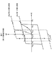
図2は、第1の実施の形態に係る2つのスピントランジスタを用いたインバータ回路の概略図である。
(Configuration of integrated circuit)
FIG. 2 is a schematic diagram of an inverter circuit using two spin transistors according to the first embodiment.
以下において、第1のスピントランジスタ2のVlowノード22及び出力ノード23、及び第2のスピントランジスタ3のVhighノード32及び出力ノード33中の丸印付の矢印は、各ノードの大多数スピン方向を示している。
In the following, the circled arrows in the V low node 22 and the
この集積回路1は、例えば、第1及び第2のスピントランジスタ2、3を用いた論理演算回路である。この論理演算回路は、例えば、インバータ回路である。集積回路1は、図2に示すように、例えば、第1及び第2のスピントランジスタ2、3を電気的に分離するための素子分離領域4が、第1及び第2のスピントランジスタ2、3の間に形成されている。この素子分離領域4は、例えば、SiO2からなる。
The
第1のスピントランジスタ2は、図2に示すように、例えば、半導体基板10に形成される。第1のスピントランジスタ2は、例えば、半導体キャップ層21と、第1のノードとしてのVlowノード22と、第2のノードとしての出力ノード23と、2DEGチャネル24と、第1のゲート電極としてのゲート電極26と、を備えて概略構成されている。
As shown in FIG. 2, the
第1のスピントランジスタ2は、例えば、ゲート電極26の下方に端子10aを有する。この端子10aは、接地(GND)されている。よって、第1のスピントランジスタ2の基板電位Vsnは、一例として、0Vである。
For example, the
半導体キャップ層21は、例えば、半導体基板10の上層部分のInAlAsであり、本実施の形態においては、ゲート絶縁膜を含む層であるものとする。半導体キャップ層21は、例えば、Vlowノード22と出力ノード23にショットキー接続している。ここで、2DEGチャネル24は、InAlAs/InGaAs/InAlAsの量子井戸構造におけるInGaAs層が2DEGチャネルとなる。なお、2DEGチャネル24は、例えば、半導体基板10がInAlAs/InGaAsを積層したヘテロ構造である場合、このInAlAs/InGaAsの界面に形成される。
The
Vlowノード22は、例えば、半導体基板10のInAlAs、InGaAs及びInGaAsの下層のInAlAsの一部を除去して形成される。Vlowノード22は、例えば、端子22aを有する。この端子22aには、例えば、電源回路から第1の電圧としての電源電圧Vlowが供給される。
The V low node 22 is formed, for example, by removing a portion of InAlAs, InGaAs, and InGaAs under the InGaAs layer of the
出力ノード23は、例えば、半導体基板10のInAlAs、InGaAs及びInGaAsの下層のInAlAsの一部を除去して形成される。出力ノード23は、例えば、端子23aを有する。この端子23aは、後述する第2のスピントランジスタ3の出力ノード33の端子33aに接続される。つまり、出力ノード23は、出力ノード33と電気的に接続されている。集積回路1は、電源電圧Vlowと第2の電圧としての電源電圧Vhighの間に第1のスピントランジスタ2と第2のスピントランジスタ3を直列に接続した回路である。
For example, the
Vlowノード22及び出力ノード23は、図2に示すように、大多数スピン方向が同じである。つまり、Vlowノード22及び出力ノード23は、磁化方向が同じである。
As shown in FIG. 2, the V low node 22 and the
Vlowノード22及び出力ノード23は、例えば、高スピン偏向材料を用いて形成される。高スピン偏向材料としては、強磁性金属及びハーフメタル強磁性体等が用いられる。
The V low node 22 and the
本実施の形態に係るVlowノード22、出力ノード23、後述するVhighノード32及び出力ノード33は、一例として、Co2MnSiを用いて形成される。
As an example, the V low node 22, the
2DEGチャネル24は、例えば、チャネル長がLである。電子5は、この2DEGチャネル24をVlowノード22から出力ノード23に向けて走行する。
The
ゲート電極26は、例えば、半導体キャップ層21上に形成される。ゲート電極26は、例えば、多結晶Siからなる。ゲート電極26は、例えば、端子26aを有する。この端子26aは、例えば、後述する第2のスピントランジスタ3のゲート電極36の端子36aに接続され、デジタル信号Vinが入力する。つまり、ゲート電極26は、ゲート電極36と電気的に接続されている。
For example, the
第2のスピントランジスタ3は、図2に示すように、例えば、半導体基板10に形成される。第2のスピントランジスタ3は、例えば、半導体キャップ層31と、第3のノードとしてのVhighノード32と、第4のノードとしての出力ノード33と、2DEGチャネル34と、第2のゲート電極としてのゲート電極36と、を備えて概略構成されている。
As shown in FIG. 2, the second spin transistor 3 is formed on the
第2のスピントランジスタ3は、例えば、ゲート電極36の下方に端子10bを有する。この端子10bは、接地(GND)されている。よって、第2のスピントランジスタ3の基板電位Vspは、一例として、0Vである。
For example, the second spin transistor 3 has a terminal 10 b below the
半導体キャップ層31は、例えば、第1のスピントランジスタ2の半導体キャップ層21と実質的に同じである。半導体キャップ層31は、例えば、Vhighノード32と出力ノード33にショットキー接続している。ここで、2DEGチャネル34は、InAlAs/InGaAs/InAlAsの量子井戸構造におけるInGaAs層が2DEGチャネルとなる。なお、2DEGチャネル34は、例えば、半導体基板10がInAlAs/InGaAsを積層したヘテロ構造である場合、このInAlAs/InGaAsの界面に形成される。
For example, the
Vhighノード32及び出力ノード33は、例えば、半導体基板10のInAlAs、InGaAs及びInGaAsの下層のInAlAsの一部を除去して形成される。また、Vhighノード32及び出力ノード33は、例えば、第1のスピントランジスタ2のVlowノード22及び出力ノード23と同じ材料を用いて形成される。また、第2のスピントランジスタ3のVhighノード32及び出力ノード33の大多数スピン方向は、相反する方向となっている。
For example, the V high node 32 and the
Vhighノード32は、例えば、端子32aを有する。この端子32aには、例えば、電源回路から電源電圧Vhighが供給される。出力ノード33は、例えば、端子33aを有する。
The V high node 32 has, for example, a
この2DEGチャネル34は、例えば、第1のスピントランジスタ2と同じチャネル長Lを有する。電子5は、この2DEGチャネル34を出力ノード33からVhighノード32に向けて走行する。
The
ゲート電極36は、例えば、半導体キャップ層31上に形成される。ゲート電極36は、例えば、第1のスピントランジスタ2のゲート電極26と同じ材料から形成される。ゲート電極36は、例えば、端子36aを有する。この端子36aには、例えば、デジタル信号Vinが入力する。
For example, the
ここで、集積回路1は、デジタル信号VlowがVinとして入力するとき、Voutとしてデジタル信号Vhighを出力し、デジタル信号VhighがVinとして入力するとき、Voutとしてデジタル信号Vlowを出力するインバータ回路である。
Here, the
以下に、本実施の形態に係る集積回路の動作について説明する。 The operation of the integrated circuit according to this embodiment will be described below.
(動作)
図3(a)は、第1の実施の形態に係るVinとしてVlowが入力した場合の第1のスピントランジスタの動作に関する概略図であり、(b)は、VinとしてVlowが入力した場合の第2のスピントランジスタの動作に関する概略図であり、(c)は、VinとしてVhighが入力した場合の第1のスピントランジスタの動作に関する概略図であり、(d)は、VinとしてVhighが入力した場合の第2のスピントランジスタの動作に関する概略図である。
(Operation)
FIG. 3A is a schematic diagram regarding the operation of the first spin transistor when V low is inputted as V in according to the first embodiment, and FIG. 3B is a diagram showing V low inputted as V in. (C) is a schematic diagram regarding the operation of the first spin transistor when V high is input as V in , and (d) is a schematic diagram regarding the operation of the second spin transistor when it is a schematic diagram of the operation of the second spin transistor in the case where V high is input as in.
(Vin=Vlowの場合)
まず、VinとしてVlowが、第1のスピントランジスタ2のゲート電極26、及び第2のスピントランジスタ3のゲート電極36に入力する。
(When V in = V low )
First, V low is input as V in to the
スピン偏極した電子5が、図3(a)に示すように、第1のスピントランジスタ2のVlowノード22から2DEGチャネル24に注入される。
The spin-polarized
この電子5は、図3(a)に示すように、2DEGチャネル24内の実効磁場によってz軸を中心に、例えば、角度πの歳差運動を行い、2DEGチャネル24と出力ノード23の境界に到達する。
As shown in FIG. 3A, the
到達した電子5は、出力ノード23の大多数スピン方向と逆向きのスピン方向となっているので、境界を反射する。
The reached
一方、スピン偏極した電子5が、図3(b)に示すように、第2のスピントランジスタ3の出力ノード33から2DEGチャネル34に注入される。
On the other hand, spin-polarized
この電子5は、図3(b)に示すように、2DEGチャネル34内の実効磁場によってz軸を中心に、例えば、角度πの歳差運動を行い、2DEGチャネル34とVhighノード32の境界に到達する。
As shown in FIG. 3B, the
到達した電子5は、Vhighノード32の大多数スピン方向と同じスピン方向となる。これは、Vhighノード32の大多数スピン方向は、出力ノード33の大多数スピン方向とは角度π異なっているからである。よって電子5は、2DEGチャネル34とVhighノード32の境界を透過する。つまり、出力ノード33の電位は、Vhighとなる。
The reached
よって、集積回路1は、Vin=Vlowの場合、第1のスピントランジスタ2には電流が流れず、第2のスピントランジスタ3には電流が流れるので、Voutからは、第2のスピントランジスタ3のVhighノード32に入力するVhighが出力される。
Thus, the integrated circuit 1, when V in = V low, the
(Vin=Vhighの場合)
まず、VinとしてVhighが、第1のスピントランジスタ2のゲート電極26、及び第2のスピントランジスタ3のゲート電極36に入力する。
(When V in = V high )
First, V high is input as V in to the
スピン偏極した電子5が、図3(c)に示すように、第1のスピントランジスタ2のVlowノード22から2DEGチャネル24に注入される。
The spin-polarized
この電子5は、図3(c)に示すように、2DEGチャネル24内の磁場によってz軸を中心に、例えば、角度2πの歳差運動を行い、2DEGチャネル24と出力ノード23の境界に到達する。
This
到達した電子5は、出力ノード23の大多数スピン方向と同じスピン方向となっているので、境界を透過する。つまり、出力ノード23の電位は、Vlowとなる。
The reached
一方、スピン偏極した電子5が、図3(d)に示すように、第2のスピントランジスタ3の出力ノード33から2DEGチャネル34に注入される。
On the other hand, spin-polarized
この電子5は、図3(d)に示すように、2DEGチャネル34内の実効磁場によってz軸を中心に、例えば、角度2πの歳差運動を行い、2DEGチャネル34とVhighノード32の境界に到達する。
The
到達した電子5は、Vhighノード32の大多数スピン方向と逆向きのスピン方向となっているので、境界で反射する。
The reached
よって、集積回路1は、Vin=Vhighの場合、第1のスピントランジスタ2には電流が流れ、第2のスピントランジスタ3には電流が流れないので、Voutからは、第1のスピントランジスタ2のVlowノード22に入力するVlowが出力される。
Thus, the integrated circuit 1, when V in = V high, a first current flows through the
従って、集積回路1は、VinとしてVlowが入力すると、VoutとしてVhighを出力し、VinとしてVhighが入力すると、VoutとしてVlowを出力するインバータ回路を構成している。 Thus, the integrated circuit 1, when V low is input as V in, and outputs a V high as V out, the V high is input as V in, and constitute an inverter circuit for outputting a V low as V out.
(第1の実施の形態の効果)
第1の実施の形態に係る集積回路1は、磁化方向が互いに同じ方向となるVlowノード22と出力ノード23を備える第1のスピントランジスタ2と、磁化方向が互いに相反する方向となるVhighノード32と出力ノード33を備える第2のスピントランジスタ3と、を直列に接続してインバータ回路を構成するため、CMOS(Complementary Metal Oxide Semiconductor)トランジスタにより構成されたインバータ回路と比べて、p型及びn型トランジスタを作り分ける必要がなく、製造工程が少なくなり、製造コストが低減する。
(Effects of the first embodiment)
In the
[第2の実施の形態]
第2の実施の形態は、第1のスピントランジスタ2の出力ノードと第2のスピントランジスタ3の出力ノードを同一のノードとする点で第1の実施の形態と異なっている。なお、以下の実施の形態において、第1の実施の形態と同様の機能及び構成を有する部分については、第1の実施の形態と同じ符号を付し、その説明は省略するものとする。
[Second Embodiment]
The second embodiment is different from the first embodiment in that the output node of the
図4は、第2の実施の形態に係る集積回路の概略図である。この集積回路1は、図4に示すように、基板電位VsnとVspが接地されていることから、第1の実施の形態における素子分離領域4を省略することが可能となる。よって、この集積回路1は、図4に示すように、第1のスピントランジスタ2の出力ノード23と、第2のスピントランジスタ3の出力ノード33を同一の領域とした出力ノード6を備えている。
FIG. 4 is a schematic diagram of an integrated circuit according to the second embodiment. As shown in FIG. 4, in the
この出力ノード6は、例えば、Vlowノード22、32と同じ材料を用いて形成される。Vhighノード32は、Vlowノード22及び出力ノード6とは大多数スピン方向が逆向きになっている。
The
また、出力ノード6は、例えば、端子6aを有する。この端子6aは、Voutを出力する。
The
以下に、本実施の形態に係る集積回路1の動作について説明する。
Hereinafter, the operation of the
(動作)
(Vin=Vlowの場合)
まず、VinとしてVlowが、第1のスピントランジスタ2のゲート電極26、及び第2のスピントランジスタ3のゲート電極36に入力する。
(Operation)
(When V in = V low )
First, V low is input as V in to the
スピン偏極した電子5が、第1のスピントランジスタ2のVlowノード22から2DEGチャネル24に注入される。
Spin-polarized
この電子5は、2DEGチャネル24内の実効磁場によってz軸を中心に、例えば、角度πの歳差運動を行い、2DEGチャネル24と出力ノード6の境界に到達する。
The
到達した電子5は、出力ノード6の大多数スピン方向と逆向きのスピン方向となっているので、境界で反射する。
The
一方、スピン偏極した電子5が、第2のスピントランジスタ3の出力ノード6から2DEGチャネル34に注入される。
On the other hand, spin-polarized
この電子5は、2DEGチャネル34内の実効磁場によってz軸を中心に、例えば、角度πの歳差運動を行い、2DEGチャネル34とVhighノード32の境界に到達する。
The
到達した電子5は、Vhighノード32の大多数スピン方向と同じスピン方向となっているので、境界を透過する。つまり、出力ノード6の電位は、Vhighとなる。
The reached
よって、集積回路1は、Vin=Vlowの場合、第1のスピントランジスタ2には電流が流れず、第2のスピントランジスタ3には電流が流れるので、Voutからは、Vhighが出力される。
Therefore, in the
(Vin=Vhighの場合)
まず、VinとしてVhighが、第1のスピントランジスタ2のゲート電極26、及び第2のスピントランジスタ3のゲート電極36に入力する。
(When V in = V high )
First, V high is input as V in to the
スピン偏極した電子5が、第1のスピントランジスタ2のVlowノード22から2DEGチャネル24に注入される。
Spin-polarized
この電子5は、2DEGチャネル24内の実効磁場によってz軸を中心に、例えば、角度2πの歳差運動を行い、2DEGチャネル24と出力ノード6の境界に到達する。
This
到達した電子5は、出力ノード6の大多数スピン方向と同じスピン方向となっているので、境界を透過する。
The reached
一方、スピン偏極した電子5が、出力ノード6から2DEGチャネル34に注入される。
On the other hand, spin-polarized
この電子5は、2DEGチャネル34内の実効磁場によってz軸を中心に、例えば、角度2πの歳差運動を行い、2DEGチャネル34とVhighノード32の境界に到達する。
This
到達した電子5は、Vhighノード32の大多数スピン方向と逆向きのスピン方向となっているので、境界で反射する。
The reached
よって、集積回路1は、Vin=Vhighの場合、第1のスピントランジスタ2には電流が流れ、第2のスピントランジスタ3には電流が流れないので、Voutからは、Vlowが出力される。
Therefore, in the
従って、集積回路1は、VinとしてVlowが入力すると、VoutとしてVhighを出力し、VinとしてVhighが入力すると、VoutとしてVlowを出力するインバータ回路を構成している。 Thus, the integrated circuit 1, when V low is input as V in, and outputs a V high as V out, the V high is input as V in, and constitute an inverter circuit for outputting a V low as V out.
(第2の実施の形態の効果)
第2の実施の形態に係る集積回路1は、基板電位Vsn、Vspが等しいことから、素子分離領域を必要とせず、素子分離領域を必要とする集積回路に比べて、設置のための面積を小さくすることができる。
(Effect of the second embodiment)
In the
[第3の実施の形態]
第3の実施の形態は、他の磁性体領域(ノード)の磁化方向とは異なる磁化方向を有する磁性体領域を、他の磁性体領域とは異なる材料によって形成する点で上記の他の実施の形態と異なっている。
[Third Embodiment]
The third embodiment is different from the above in that the magnetic material region having a magnetization direction different from the magnetization direction of the other magnetic material region (node) is formed of a material different from that of the other magnetic material region. The form is different.
(集積回路1の構成)
図5(a)は、第3の実施の形態に係る集積回路の概略図であり、(b)は、集積回路の上面図である。
(Configuration of integrated circuit 1)
FIG. 5A is a schematic diagram of an integrated circuit according to the third embodiment, and FIG. 5B is a top view of the integrated circuit.
本実施の形態に係る集積回路1は、図5(a)に示すVhighノード32が、Vlowノード22及び出力ノード6とは、異なる材料から形成されている。磁性体は、不純物の含有量を減じる、又は、磁性体のアニール条件を変えること等により、内部歪みを変え、保磁力を変化させることができる。よって、異なる材料としては、一例として、ドーピング比の異なるNiFeが用いられる。
In the
以下に、本実施の形態に係る集積回路1の製造方法について説明する。
Below, the manufacturing method of the
(集積回路の製造方法)
図6A(a)〜図6B(o)は、第3の実施の形態に係る集積回路の製造工程を示す要部断面図である。
(Manufacturing method of integrated circuit)
FIGS. 6A (a) to 6B (o) are cross-sectional views of relevant parts showing manufacturing steps of the integrated circuit according to the third embodiment.
まず、分子線エピタキシー法等により、InP基板上にInAlAs、InGaAs及びInGaAsを順に積層させて半導体基板10を形成する。この半導体基板10のInGaAs層を2DEGチャネル前駆体層60とする。また、半導体基板10上層のInAlAsを半導体キャップ層前駆体層61とする。
First, a
次に、図6A(a)に示すように、フォトリソグラフィ法及びRIE(Reactive Ion Etching)法等により、素子分離領域4を形成し、続いて、保護膜62を形成する。
Next, as shown in FIG. 6A, an
次に、図6A(b)に示すように、フォトリソグラフィ法及びRIE法等により、保護膜62上にマスク膜63を形成する。このマスク膜63は、Vlowノード22に対応する位置に開口63aが形成され、出力ノード6に対応する位置に開口63bが形成される。
Next, as shown in FIG. 6A (b), a
次に、図6A(c)に示すように、RIE法等により、マスク膜63をマスクとして異方性エッチングを行い、開口63a及び開口63b内の保護膜62及び2DEGチャネル前駆体層60と、半導体基板10の一部を除去する。
Next, as shown in FIG. 6A (c), anisotropic etching is performed using the
次に、図6A(d)に示すように、マスク膜63を除去する。
Next, as shown in FIG. 6A (d), the
次に、図6A(e)に示すように、CVD(Chemical Vapor Deposition)法等により、第1の磁性体金属64を開口63a、開口63b及び保護膜62上に形成する。この第1の磁性体金属64は、例えば、上記に記載のホイスラー合金である。
Next, as shown in FIG. 6A (e), a first magnetic metal 64 is formed on the
次に、図6A(f)に示すように、CMP(Chemical Mechanical Polishing)法等によって平坦化処理を行い、保護膜62上の第1の磁性体金属64を除去する。この平坦化処理により、開口63aには、第1の磁性体金属64からなる磁性体領域65が形成され、開口63bには、第1の磁性体金属64からなる磁性体領域66が形成される。
Next, as shown in FIG. 6A (f), a planarization process is performed by a CMP (Chemical Mechanical Polishing) method or the like to remove the first magnetic metal 64 on the
次に、図6A(g)に示すように、フォトリソグラフィ法及びRIE法等により、保護膜62、磁性体領域65及び磁性体領域66上にマスク膜67を形成する。このマスク膜67は、Vhighノード32に対応する位置に開口67aが形成される。
Next, as shown in FIG. 6A (g), a
次に、図6A(h)に示すように、RIE法等により、マスク膜67をマスクとして異方性エッチングを行い、開口67a内の保護膜62及び2DEGチャネル前駆体層60と、半導体基板10の一部を除去する。
Next, as shown in FIG. 6A (h), anisotropic etching is performed using the
次に、図6B(i)に示すように、CVD法等により、第2の磁性体金属68を開口67a及び保護膜62上に形成する。この第2の磁性体金属68は、例えば、上記に記載のホイスラー合金である。
Next, as shown in FIG. 6B (i), a second magnetic metal 68 is formed on the opening 67a and the
次に、図6B(j)に示すように、CMP法等によって平坦化処理を行い、保護膜62上の第2の磁性体金属68を除去する。この平坦化処理により、開口67aには、第2の磁性体金属68からなる磁性体領域69が形成される。
Next, as shown in FIG. 6B (j), a planarization process is performed by a CMP method or the like, and the second magnetic metal metal 68 on the
次に、図6B(k)に示すように、ウエットエッチング法等により、保護膜62を選択的に除去する。
Next, as shown in FIG. 6B (k), the
次に、CVD法等により、素子分離領域4、半導体キャップ層前駆体層61、磁性体領域65、磁性体領域66及び磁性体領域69上に絶縁膜を堆積させる。続いて、図6B(l)に示すように、RIE法等による等方性エッチングを行うことにより、磁性体領域65、磁性体領域66及び磁性体領域69の側面に側壁70を形成する。
Next, an insulating film is deposited on the
次に、図6B(m)に示すように、CVD法等により、素子分離領域4、半導体キャップ層前駆体層61、磁性体領域65、磁性体領域66、磁性体領域69及び側壁70上にメタルゲート電極前駆体膜71を形成する。このメタルゲート電極前駆体膜71は、例えば、Ta、Ru等の金属材料の単層を含んで形成されるか、又は、金属材料を積層させた構造を含んで形成される。なお、積層させた構造は、例えば、Ti/Auを含んで積層させた構造、又はTiN/Pt/Auを含んで積層させた構造である。
Next, as shown in FIG. 6B (m), on the
次に、図6B(n)に示すように、フォトリソグラフィ法及びRIE法等により、磁性体領域69と磁性体領域65の間、及び磁性体領域65と磁性体領域66の間にゲートマスク72を形成する。
Next, as shown in FIG. 6B (n), a gate mask 72 is formed between the
次に、図6B(o)及び図5(b)に示すように、RIE法等により、ゲートマスク72をマスクとしてメタルゲート電極前駆体膜71を除去する。ここで、磁性体領域65は、集積回路1のVlowノード22として用いられる。磁性体領域66は、出力ノード6として用いられる。磁性体領域69は、Vhighノード32として用いられる。続いて、Vlowノード22、出力ノード6及びVhighノード32に磁化を形成させる。以下では、この磁化を形成させる方法について説明する。
Next, as shown in FIGS. 6B (o) and 5 (b), the metal gate
(磁化を形成させる方法について)
図7は、第3の実施の形態に係る第1の磁性体金属及び第2の磁性体金属の磁化曲線の概略図である。図7の縦軸は磁化の強さMであり、横軸は磁場の強さHである。図7に実線で示す第1の磁化曲線64aは、第1の磁性体金属64の磁化曲線であり、一点鎖線で示す第2の磁化曲線68aは、第2の磁性体金属68の磁化曲線である。以下では、外部から印加される磁場Hを0、H1、0、H2、0の順に変化させたときの第1の磁性体金属64及び第2の磁性体金属68の磁化について説明する。なお、磁場の強さは、図7の磁場Hの右側を正とすると、Hc4<H2<Hc3<0<Hc2<Hc1<H1となっている。磁場H1、Hc1、Hc2の磁場の方向は、Hc3、H2、Hc4の磁場の方向とは逆となっている。
(About the method of forming magnetization)
FIG. 7 is a schematic diagram of magnetization curves of the first magnetic metal and the second magnetic metal according to the third embodiment. The vertical axis in FIG. 7 is the magnetization strength M, and the horizontal axis is the magnetic field strength H. A first magnetization curve 64 a indicated by a solid line in FIG. 7 is a magnetization curve of the first magnetic metal 64, and a second magnetization curve 68 a indicated by an alternate long and short dash line is a magnetization curve of the second magnetic metal 68. is there. Hereinafter, the magnetization of the first magnetic metal 64 and the second magnetic metal 68 when the externally applied magnetic field H is changed in the order of 0, H 1 , 0, H 2 , 0 will be described. Incidentally, the strength of the magnetic field, when the right magnetic field H in FIG. 7 and positive, and has a H c4 <H 2 <H c3 <0 <H c2 <H c1 <
また、図7に示す点Aは磁場H1における第1の磁化曲線64a上の点である。点Bは磁場ゼロにおける第1の磁化曲線64a上の点である。点Cは磁場H2における第1の磁化曲線64a上の点である。 Also, A point shown in FIG. 7 is a point on the first magnetization curve 64a in a magnetic field H 1. Point B is a point on the first magnetization curve 64a at zero magnetic field. Point C is a point on the first magnetization curve 64a in a magnetic field H 2.
さらに、図7に示す点aは、磁場H1における第2の磁化曲線68a上の点である。点b及び点eは磁場ゼロにおいて磁性体が磁化している際の第2の磁化曲線68a上の点である。点cは磁場Hc3における第2の磁化曲線68a上の点である。点dは、磁場H2における第2の磁化曲線68a上の点である。 Furthermore, a point illustrated in FIG. 7 is a point on the second magnetization curve 68a in a magnetic field H 1. Points b and e are points on the second magnetization curve 68a when the magnetic material is magnetized at zero magnetic field. Point c is a point on the second magnetization curve 68a in the magnetic field Hc3 . Point d is a point on the second magnetization curve 68a in a magnetic field H 2.
まず、外部から磁場H1を、磁化Mがゼロの状態であるVlowノード22、出力ノード6及びVhighノード32に印加する。この外部磁場の印加は、例えば、Vlowノード22、出力ノード6及びVhighノード32等が形成された半導体基板10に行われる。
First, a magnetic field H 1 is applied from the outside to the V low node 22, the
まず、第1の磁性体金属64の磁化について説明する。図7に示すように、印加される磁場が、磁場ゼロから磁場H1まで増加するにつれ、第1の磁性体金属64の磁化は、ゼロの状態から初期磁化曲線上を移動し、さらに、磁場H1における第1の磁化曲線64a上の点Aまで増加する。 First, the magnetization of the first magnetic metal 64 will be described. As shown in FIG. 7, as the applied magnetic field increases from magnetic field zero to magnetic field H 1 , the magnetization of the first magnetic metal metal 64 moves on the initial magnetization curve from the zero state. increases in H 1 to the point a on the first magnetization curve 64a.
続いて、印加する磁場H1をゼロにすると、第1の磁性体金属64の磁化は、点Aから初期磁化曲線上を戻らず、すなわち、ゼロとならず、磁化M軸上のゼロではない点Bに到達する。この磁化M軸上の点Bは、残留磁化の大きさを示している。 Subsequently, when the magnetic field H 1 is applied to zero, the magnetization of the first magnetic metal 64 is not returned on the initial magnetization curve from point A, i.e., not zero, a non-zero on the magnetization M axis Point B is reached. A point B on the magnetization M axis indicates the magnitude of the residual magnetization.
続いて、印加される磁場が、磁場ゼロから磁場H2まで増加するにつれ、第1の磁性体金属64の磁化は、徐々に残留磁化が小さくなるものの磁化方向が逆転することはなく、第1の磁化曲線64a上の点Cに到達する。 Subsequently, the applied magnetic field is, as it increases from zero magnetic field to the magnetic field H 2, magnetization of the first magnetic metal 64 is not that the magnetization direction of which gradually residual magnetization decreases reversed, first The point C on the magnetization curve 64a is reached.
続いて、印加する磁場H2をゼロとすると、第1の磁性体金属64の磁化は、第1の磁化曲線64aに沿って徐々に増加し、磁場ゼロにおいて残留磁化Bを有することとなる。 Subsequently, when the magnetic field H 2 is applied to zero, the magnetization of the first magnetic metal 64 along the first magnetization curve 64a gradually increases, it will have a residual magnetization B at zero magnetic field.
一方、第2の磁性体金属68の磁化は、図7に示すように、印加される磁場が、磁場ゼロから磁場H1まで増加するにつれ、ゼロの状態から初期磁化曲線上を移動し、さらに、磁場H1における第1の磁化曲線64a上の点aまで増加する。ここで、点aにおける磁化Mは、点Aにおける磁化Mよりも大きい。 On the other hand, as shown in FIG. 7, the magnetization of the second magnetic metal 68 moves from the zero state on the initial magnetization curve as the applied magnetic field increases from the magnetic field zero to the magnetic field H 1. increases to a point on the first magnetization curve 64a in a magnetic field H 1. Here, the magnetization M at the point a is larger than the magnetization M at the point A.
続いて、印加する磁場H1をゼロとすると、第2の磁性体金属68の磁化は、点aから初期磁化曲線上を戻らず、磁化M軸上のゼロではない点bに到達する。この磁化M軸上の点bは、残留磁化の大きさを示している。ここで、点bにおける残留磁化は、点Bにおける残留磁化よりも大きい。 Subsequently, when the magnetic field H 1 is applied to zero, the magnetization of the second magnetic metal 68 is not returned on the initial magnetization curve from point a, and reaches the point b is not zero on the magnetization M axis. A point b on the magnetization M axis indicates the magnitude of the residual magnetization. Here, the residual magnetization at point b is larger than the residual magnetization at point B.
続いて、印加される磁場が、磁場ゼロから磁場H2まで増加するにつれ、第2の磁性体金属68の磁化は、徐々に残留磁化が小さくなり、磁場がHc3のとき、磁化方向が逆転して点cに到達し、さらに、点cから磁化の強さが増加した点dに到達する。この点c及びdにおける磁化方向は、第1の磁化曲線64a上の点B及び第2の磁化曲線68a上の点bにおける磁化方向とは逆となっている。 Then, as the applied magnetic field is increased from zero magnetic field to the magnetic field H 2, magnetization of the second magnetic metal 68 is gradually residual magnetization is reduced, when the magnetic field is H c3, the magnetization direction reversal The point c is reached, and further, the point d is reached from the point c where the strength of magnetization is increased. The magnetization directions at points c and d are opposite to the magnetization directions at point B on the first magnetization curve 64a and point b on the second magnetization curve 68a.
続いて、印加する磁場H2をゼロとすると、第2の磁性体金属68の磁化は、磁化方向を反転させることなく、第2の磁化曲線68aに沿って徐々に減少し、磁場ゼロにおいて残留磁化eを有することとなる。 Subsequently, when the magnetic field H 2 is applied to zero, the magnetization of the second magnetic metal 68, without inverting the magnetization direction gradually decreases along the second magnetization curve 68a, the residual in zero magnetic field It will have magnetization e.
従って、印加する磁場Hを0、H1、0、H2、0と順に変化させることにより、第1の磁性体金属64と第2の磁性体金属68とに、相反する方向の磁化を同時に形成することができる。 Therefore, by changing the applied magnetic field H in the order of 0, H 1 , 0, H 2 , 0, the first magnetic metal 64 and the second magnetic metal 68 are simultaneously magnetized in opposite directions. Can be formed.
次に、周知の工程を経て、集積回路1を得る。なお、上記の磁化させる工程では、磁場Hを0、H1、0、H2、0の順に変化させたが、0、H2、0、H1、0の順に変化させても良い。
Next, the
(第3の実施の形態の効果)
第3の実施の形態に係る集積回路1は、同じ磁化方向を有するVlowノード22、出力ノード6と、Vlowノード22、出力ノード6とは相反する磁化方向を有するVhighノード32を同時に磁化することができるので、局所的に磁化を行う場合と比べて、工程が少なく、集積回路1を含む半導体装置の製造コストを抑制することができる。
(Effect of the third embodiment)
In the
[第4の実施の形態]
第4の実施の形態は、磁化方向が異なるVhighノードの体積と、他のVlowノード及び出力ノードの体積を異なる体積とする点で上記の他の実施の形態と異なっている。なお、以下では、Vhighノード32の体積を、他のVlowノード22及び出力ノード6の体積よりも小さいものとしたが、これに限定されず、Vhighノード32の体積を、他のVlowノード22及び出力ノード6の体積よりも大きくしても良い。
[Fourth Embodiment]
The fourth embodiment is different from the other embodiments described above in that the volume of the V high node having a different magnetization direction and the volume of the other V low node and the output node are different volumes. In the following, the volume of the V high
(集積回路1の構成)
図8(a)は、第4の実施の形態に係る集積回路の概略図であり、(b)は、磁性体金属の磁化曲線の概略図である。図8(b)に実線で示す第1の磁化曲線8aは、体積がVhighノード32よりも大きいVlowノード22及び出力ノード6を形成する磁性体金属の磁化曲線であり、一点鎖線で示す第2の磁化曲線8bは、Vhighノード32を形成する磁性体金属の磁化曲線である。以下では、外部から印加される磁場Hを、第3の実施の形態と同様に、0、H1、0、H2、0の順に変化させたときの磁化について説明する。なお、磁場の強さは、図7と同様に、Hc4<H2<Hc3<0<Hc2<Hc1<H1となっている。
(Configuration of integrated circuit 1)
FIG. 8A is a schematic diagram of an integrated circuit according to the fourth embodiment, and FIG. 8B is a schematic diagram of a magnetization curve of a magnetic metal. A first magnetization curve 8a indicated by a solid line in FIG. 8B is a magnetization curve of the magnetic metal forming the V low node 22 and the
また、図8(b)に示す点Aは磁場H1における第1の磁化曲線8a上の点である。点Bは磁場ゼロにおける第1の磁化曲線8a上の点である。点Cは磁場H2における第1の磁化曲線8a上の点である。 Also, A point shown in FIG. 8 (b) is a point on the first magnetization curve 8a in the magnetic field H 1. Point B is a point on the first magnetization curve 8a at zero magnetic field. Point C is a point on the first magnetization curve 8a in the magnetic field H 2.
さらに、図8(b)に示す点aは、磁場H1における第2の磁化曲線8b上の点である。点b及び点eは磁場ゼロにおける第2の磁化曲線8b上の点である。点cは磁場Hc3における第2の磁化曲線8b上の点である。点dは、磁場H2における第2の磁化曲線8b上の点である。 Furthermore, a point shown in FIG. 8 (b) is a point on the second magnetization curve 8b in the magnetic field H 1. Points b and e are points on the second magnetization curve 8b at zero magnetic field. Point c is a point on the second magnetization curve 8b in the magnetic field Hc3 . Point d is a point on the second magnetization curve 8b in a magnetic field H 2.
本実施の形態に係る集積回路1は、第2のスピントランジスタ3のVhighノード32の体積が、Vhighノード32の磁化方向と逆向きの磁化方向を有するVlowノード22及び出力ノード6の体積よりも小さくなっている他は、第2の実施の形態と同じ構成を有している。なお、Vlowノード22、出力ノード6及びVhighノード32は、例えば、同じ材料から形成されるものとする。
Vlowノード22及び出力ノード6よりも体積が小さいVhighノード32は、図8(a)に示すように、磁化が反転する際の磁場の強さHc3が、Vlowノード22及び出力ノード6の磁化が反転する磁場の強さHc4よりも小さい。これは、体積が小さい方が、磁化が反転し易いことに起因している。従って、初期磁化曲線を抜けてヒステリシスループの磁気飽和に達するまでの磁場H1、及び磁場Hc3と磁場Hc4との間の値となる磁場H2を印加することにより、Vlowノード22及び出力ノード6の磁化と、Vlowノード22及び出力ノード6の磁化方向と相反する磁化方向を有するVhighノード32の磁化とを同時に行うことができる。
V low node 22 and output node V high node 32 volume is less than 6, as shown in FIG. 8 (a), the intensity H c3 of the magnetic field when the magnetization is reversed, V low
なお、第1の実施の形態に係る集積回路において、磁化方向が他の磁性体領域と異なる磁性体領域(例えば、出力ノード33)の体積を他の磁性体領域の体積と異なるものとしても良い。 In the integrated circuit according to the first embodiment, the volume of the magnetic region (for example, the output node 33) whose magnetization direction is different from that of the other magnetic region may be different from the volume of the other magnetic region. .
(第4の実施の形態の効果)
第4の実施の形態に係る集積回路1は、異なる磁化方向を有するVlowノード22、出力ノード6及びVhighノード32を同時に磁化することができるので、磁化方向に応じて局所的に磁化を行う場合と比べて、工程が少なく、集積回路1を含む半導体装置の製造コストを抑制することができる。
(Effect of the fourth embodiment)
Since the
[第5の実施の形態]
第5の実施の形態は、スピントランジスタの上方に形成された配線を利用して磁性体領域を磁化する点で上記の他の実施の形態と異なっている。
[Fifth Embodiment]
The fifth embodiment is different from the other embodiments described above in that the magnetic region is magnetized using the wiring formed above the spin transistor.
(集積回路1の構成)
図9は、第5の実施の形態に係る集積回路の概略図である。本実施の形態に係る集積回路1の主な構成は、第4の実施の形態に係る集積回路と同様であるが、さらに、第1のスピントランジスタ2及び第2のスピントランジスタ3上に層間絶縁膜9と、この層間絶縁膜9上に配線90が形成されている。
(Configuration of integrated circuit 1)
FIG. 9 is a schematic diagram of an integrated circuit according to the fifth embodiment. The main configuration of the
Vhighノード32は、第4の実施の形態において示すように、Vlowノード22及び出力ノード6と比べて、体積が小さいことからその保磁力も小さい。よって、図9に示すように、Vhighノード32の上方に配線90を形成し、この配線90に電流を流すことで磁場Hを発生させ、この磁場Hによって磁化を行う。なお、他の磁性体領域の上方に、配線を設け、この配線に電流を流すことにより、磁化を行っても良い。
As shown in the fourth embodiment, the V high node 32 is smaller in volume and smaller in coercive force than the V low node 22 and the
(第5の実施の形態の効果)
第5の実施の形態に係る集積回路1は、磁性体領域の上方に配線を備えているので、半導体装置を製造した後であっても、磁性体領域の磁化を行うことができる。集積回路1は、例えば、外部の擾乱磁場及び温度の揺らぎ等による、磁化の反転及び磁化の消失等が起こったとしても、不具合が生じた磁性体領域の上方に位置する配線に電流が流されることにより発生する磁場によって、半導体装置の製造終了後であっても再度磁化を行うことができる。また、集積回路1は、例えば、定期的に配線に電流を流すことで、磁化の消失等の不具合を未然に防止することができる。
(Effect of 5th Embodiment)
Since the
[第6の実施の形態]
第6の実施の形態は、上記に記載のスピントランジスタを組み合わせてNAND回路を構成する点で上記の他の実施の形態と異なっている。
[Sixth Embodiment]
The sixth embodiment is different from the other embodiments described above in that a NAND circuit is configured by combining the spin transistors described above.
(NAND回路100aの構成)
図10(a)は、第6の実施の形態に係るNAND回路の概略図であり、(b)は、NAND回路の論理演算表である。本実施の形態に係るNAND回路100aは、素子分離領域4を挟んでスピントランジスタで構成された第1の素子101及び第2の素子102が電源電圧Vlowと電源電圧Vhighの間に直列に接続されている。
(Configuration of NAND circuit 100a)
FIG. 10A is a schematic diagram of a NAND circuit according to the sixth embodiment, and FIG. 10B is a logical operation table of the NAND circuit. In the NAND circuit 100a according to the present embodiment, the
第1の素子101は、図10(a)に示すように、Vlowノード200、中間ノード201b及び出力ノード202bが、それぞれのチャネル長がLとなるように半導体基板10に並んで形成されている。Vlowノード200と中間ノード201bの間には、2DEGチャネル203が形成され、中間ノード201bと出力ノード202bの間には、2DEGチャネル204が形成されている。Vlowノード200、中間ノード201b及び出力ノード202bの大多数スピン方向は、同じ方向を有する。
As shown in FIG. 10A, the
2DEGチャネル203の上方には、半導体キャップ層205を挟んでゲート電極209が形成されている。
A
2DEGチャネル204の上方には、半導体キャップ層206を挟んでゲート電極210が形成されている。
A gate electrode 210 is formed above the
Vlowノード200は、端子200aを有し、電源回路から電源電圧Vlowが供給される。出力ノード202bは、端子202aを有する。
The V low node 200 has a terminal 200a and is supplied with the power supply voltage V low from the power supply circuit. The
ゲート電極209は、端子209aを有する。ゲート電極210は、端子210aを有する。
The
第1の素子101の半導体基板10には、端子101aが形成されている。第1の素子101の基板電位V1は、一例として、接地されているので0Vである。
A terminal 101 a is formed on the
第2の素子102は、図10(a)に示すように、Vhighノード300b、出力ノード301b及びVhighノード302が、それぞれチャネル長がLとなるように半導体基板10に並んで形成されている。Vhighノード300bと出力ノード301bの間には、2DEGチャネル303が形成され、出力ノード301bとVhighノード302の間には、2DEGチャネル304が形成されている。
As shown in FIG. 10A, the
2DEGチャネル303の上方には、半導体キャップ層305を挟んでゲート電極309が形成されている。
A
2DEGチャネル304の上方には、半導体キャップ層306を挟んでゲート電極310が形成されている。
A
Vhighノード300bは、端子300aを有する。出力ノード301bは、端子301aを有し、第1の素子101の出力ノード202bの端子202aに接続され、Voutを出力する。Vhighノード302は、端子302aを有し、電源回路から電源電圧Vhighが供給される。この端子302aは、Vhighノード300bの端子300aに接続されている。つまり、Vhighノード300b及びVhighノード302の電位は、同電位となる。第2の素子102の基板電位V2は、一例として、接地されているので0Vである。
The V high node 300b has a terminal 300a. The output node 301b has a terminal 301a, is connected to the terminal 202a of the
Vhighノード300b及びVhighノード302は、同じ大多数スピン方向を有する。出力ノード301bの大多数スピン方向は、Vhighノード300b及びVhighノード302の大多数スピン方向と逆向きとなっている。なお、本実施の形態に係る第2の素子102のVhighノード300b及びVhighノード302は、第1の素子101のVlowノード200、中間ノード201b及び出力ノード202bの大多数スピン方向と同じであるが、これに限定されず、逆方向であっても良い。その際、出力ノード301bは、Vlowノード200、中間ノード201b及び出力ノード202bの大多数スピン方向と同じ方向となる。
The V high node 300b and the V high node 302 have the same majority spin direction. The majority spin direction of the output node 301 b is opposite to the majority spin direction of the V high node 300 b and the V high node 302. Note that the V high node 300b and the V high node 302 of the
ゲート電極309は、端子309aを有する。この端子309aは、第1の素子101のゲート電極210の端子210aと接続され、デジタル信号Vin2が入力する。ゲート電極310は、端子310aを有する。この端子310aは、第1の素子101のゲート電極209の端子209aと接続され、デジタル信号Vin1が入力する。
The
第2の素子102の半導体基板10には、端子102aが形成されている。
A terminal 102 a is formed on the
以下に、図10(b)に示す論理演算表に基づいてNAND回路100aの動作について説明する。 The operation of the NAND circuit 100a will be described below based on the logical operation table shown in FIG.
(動作)
以下では、ゲート電極に電圧Vlowが印加された場合、チャネル長Lを有する2DEGチャネルを走行する電子5は、例えば、角度πの歳差運動を行う。また、ゲート電極に電圧Vhighが印加された場合、チャネル長Lを有する2DEGチャネルを走行する電子5は、例えば、角度2πの歳差運動を行う。
(Operation)
Hereinafter, when the voltage V low is applied to the gate electrode, the
(Vin1=Vlow、Vin2=Vlowの場合)
まず、Vin1としてVlowが、第1の素子101のゲート電極209、及び第2の素子102のゲート電極310に入力する。また、Vin2としてVlowが、第1の素子101のゲート電極210、及び第2の素子102のゲート電極309に入力する。
(When V in1 = V low , V in2 = V low )
First, V low is input as V in1 to the
スピン偏極した電子5が、第1の素子101のVlowノード200から2DEGチャネル203に注入される。
Spin-polarized
この電子5は、2DEGチャネル203内の実効磁場によってz軸を中心に、例えば、角度πの歳差運動を行い、2DEGチャネル203と中間ノード201bの境界に達する。
The
到達した電子5は、中間ノード201bの大多数スピン方向と角度π異なるスピン方向となっているので、境界で反射する。つまり、電子5は、中間ノード201bを透過できないので、第1の素子101には、電流が流れない。
The reached
一方、スピン偏極した電子5が、第2の素子102の出力ノード301bから2DEGチャネル303及び2DEGチャネル304に注入される。
On the other hand, spin-polarized
この電子5は、2DEGチャネル303内の実効磁場によってz軸を中心に、例えば、角度πの歳差運動を行い、2DEGチャネル303とVhighノード300bの境界に到達する。
This
到達した電子5は、Vhighノード300bの大多数スピン方向と同じスピン方向となっているので、境界を透過する。これは、Vhighノード300bと出力ノード301bの大多数スピン方向が、角度π異なっていることに起因している。
The reached
また、電子5は、2DEGチャネル304内の実効磁場によってz軸を中心に、例えば、角度πの歳差運動を行い、2DEGチャネル304とVhighノード302の境界に到達する。
Further, the
到達した電子5は、Vhighノード302の大多数スピン方向と角度π異なるスピン方向となっているので、境界を透過する。つまり、出力ノード301bは、電位がVhighとなる。
The reached
よって、集積回路1は、Vin1=Vlow、Vin2=Vlowの場合、第1の素子101には電流が流れず、第2の素子102には電流が流れるので、Voutからは、Vhighが出力される。
Thus, the integrated circuit 1, when V in1 = V low, V in2 = V low, no current flows through the
(Vin1=Vlow、Vin2=Vhighの場合)
まず、Vin1としてVlowが、第1の素子101のゲート電極209、及び第2の素子102のゲート電極310に入力する。また、Vin2としてVhighが、第1の素子101のゲート電極210、及び第2の素子102のゲート電極309に入力する。
(When V in1 = V low and V in2 = V high )
First, V low is input as V in1 to the
スピン偏極した電子5が、第1の素子101のVlowノード200から2DEGチャネル203に注入される。
Spin-polarized
この電子5は、2DEGチャネル203内の実効磁場によってz軸を中心に、例えば、角度πの歳差運動を行い、2DEGチャネル203と中間ノード201bの境界に達する。
The
到達した電子5は、中間ノード201bの大多数スピン方向と角度π異なるスピン方向となっているので、境界で反射する。つまり、電子5は、中間ノード201bを透過できないので、第1の素子101には、電流が流れない。
The reached
一方、スピン偏極した電子5が、第2の素子102の出力ノード301bから2DEGチャネル303及び2DEGチャネル304に注入される。
On the other hand, spin-polarized
この電子5は、2DEGチャネル303内の実効磁場によってz軸を中心に、例えば、角度2πの歳差運動を行い、2DEGチャネル303とVhighノード300bの境界に到達する。
This
到達した電子5は、Vhighノード300bの大多数スピン方向と逆向きのスピン方向となっているので、境界を反射する。
The reached
また、電子5は、2DEGチャネル304内の実効磁場によってz軸を中心に、例えば、角度πの歳差運動を行い、2DEGチャネル304とVhighノード302の境界に到達する。
Further, the
到達した電子5は、Vhighノード302の大多数スピン方向と同じスピン方向となっているので、境界を透過する。つまり、出力ノード301bは、電位がVhighとなる。
The reached
よって、集積回路1は、Vin1=Vlow、Vin2=Vlowの場合、第1の素子101には電流が流れず、第2の素子102には電流が流れるので、Voutからは、Vhighが出力される。
Thus, the integrated circuit 1, when V in1 = V low, V in2 = V low, no current flows through the
(Vin1=Vhigh、Vin2=Vlowの場合)
まず、Vin1としてVhighが、第1の素子101のゲート電極209、及び第2の素子102のゲート電極310に入力する。また、Vin2としてVlowが、第1の素子101のゲート電極210、及び第2の素子102のゲート電極309に入力する。
(When V in1 = V high and V in2 = V low )
First, V high is input as V in1 to the
スピン偏極した電子5が、第1の素子101のVlowノード200から2DEGチャネル203に注入される。
Spin-polarized
この電子5は、2DEGチャネル203内の実効磁場によってz軸を中心に、例えば、角度2πの歳差運動を行い、2DEGチャネル203と中間ノード201bの境界に達する。
This
到達した電子5は、中間ノード201bの大多数スピン方向と角度2π異なるスピン方向となっているので、境界を透過する。
The reached
続いて、スピン偏極した電子5が、第1の素子101の中間ノード201bから2DEGチャネル204に注入される。
Subsequently, spin-polarized
この電子5は、2DEGチャネル204内の実効磁場によってz軸を中心に、例えば、角度πの歳差運動を行い、2DEGチャネル204と出力ノード202bの境界に達する。
This
到達した電子5は、出力ノード202bの大多数スピン方向と角度π異なるスピン方向となっているので、境界を反射する。つまり、第1の素子101には、電流が流れない。
The reached
一方、スピン偏極した電子5が、第2の素子102の出力ノード301bから2DEGチャネル303及び2DEGチャネル304に注入される。
On the other hand, spin-polarized
この電子5は、2DEGチャネル303内の実効磁場によってz軸を中心に、例えば、角度πの歳差運動を行い、2DEGチャネル303とVhighノード300bの境界に到達する。
This
到達した電子5は、Vhighノード300bの大多数スピン方向と同じスピン方向となっているので、境界を透過する。
The reached
また、電子5は、2DEGチャネル304内の実効磁場によってz軸を中心に、例えば、角度2πの歳差運動を行い、2DEGチャネル304とVhighノード302の境界に到達する。
The
到達した電子5は、Vhighノード302の大多数スピン方向と逆向きのスピン方向となっているので、境界を反射する。しかし、出力ノード301bとVhighノード300b間には、電流が流れるので、出力ノード301bの電位はVhighとなる。
The reached
よって、集積回路1は、Vin1=Vhigh、Vin2=Vlowの場合、第1の素子101には電流が流れず、第2の素子102の出力ノード301bとVhighノード302間に電流が流れるので、Voutからは、Vhighが出力される。
Therefore, in the
(Vin1=Vhigh、Vin2=Vhighの場合)
まず、Vin1としてVhighが、第1の素子101のゲート電極209、及び第2の素子102のゲート電極310に入力する。また、Vin2としてVhighが、第1の素子101のゲート電極210、及び第2の素子102のゲート電極309に入力する。
(When V in1 = V high and V in2 = V high )
First, V high is input as V in1 to the
スピン偏極した電子5が、第1の素子101のVlowノード200から2DEGチャネル203に注入される。
Spin-polarized
この電子5は、2DEGチャネル203内の実効磁場によってz軸を中心に、例えば、角度2πの歳差運動を行い、2DEGチャネル203と中間ノード201bの境界に達する。
This
到達した電子5は、中間ノード201bの大多数スピン方向と角度2π異なるスピン方向となっているので、境界を透過する。
The reached
続いて、スピン偏極した電子5が、第1の素子101の中間ノード201bから2DEGチャネル204に注入される。
Subsequently, spin-polarized
この電子5は、2DEGチャネル204内の実効磁場によってz軸を中心に、例えば、角度2πの歳差運動を行い、2DEGチャネル204と出力ノード202bの境界に達する。
This
到達した電子5は、出力ノード202bの大多数スピン方向と角度2π異なるスピン方向となっているので、境界を透過する。つまり、出力ノード202bは、電位がVlowとなる。
The reached
一方、スピン偏極した電子5が、第2の素子102の出力ノード301bから2DEGチャネル303及び2DEGチャネル304に注入される。
On the other hand, spin-polarized
この電子5は、2DEGチャネル303内の実効磁場によってz軸を中心に、例えば、角度2πの歳差運動を行い、2DEGチャネル303とVhighノード300bの境界に到達する。
This
到達した電子5は、Vhighノード300bの大多数スピン方向と逆向きのスピン方向となっているので、境界を反射する。
The reached
また、電子5は、2DEGチャネル304内の実効磁場によってz軸を中心に、例えば、角度2πの歳差運動を行い、2DEGチャネル304とVhighノード302の境界に到達する。
The
到達した電子5は、Vhighノード302の大多数スピン方向と逆向きのスピン方向となっているので、境界を反射する。つまり、第2の素子102には、電流が流れない。
The reached
よって、集積回路1は、Vin1=Vhigh、Vin2=Vhighの場合、第1の素子101に電流が流れ、第2の素子102には電流が流れないので、Voutからは、Vlowが出力される。
Thus, the integrated circuit 1, when V in1 = V high, V in2 = V high, current flows through the
従って、NAND回路100aは、図10(b)に示す論理演算表を満足するので、NAND回路を構成している。 Therefore, the NAND circuit 100a satisfies the logical operation table shown in FIG. 10B, and thus constitutes a NAND circuit.
(第6の実施の形態の効果)
第6の実施の形態に係るNAND回路100aは、CMOSトランジスタにより構成されたNAND回路と比べて、p型及びn型トランジスタを作り分ける必要がなく、製造工程が少なくなり、製造コストが低減する。
(Effect of 6th Embodiment)
In the NAND circuit 100a according to the sixth embodiment, it is not necessary to make p-type and n-type transistors separately, as compared with a NAND circuit constituted by CMOS transistors, and the manufacturing process is reduced and the manufacturing cost is reduced.
[第7の実施の形態]
第7の実施の形態は、上記に記載のスピントランジスタを組み合わせてNOR回路を構成する点で上記の他の実施の形態と異なっている。
[Seventh Embodiment]
The seventh embodiment is different from the other embodiments described above in that a NOR circuit is configured by combining the spin transistors described above.
(NOR回路100bの構成)
図11(a)は、第7の実施の形態に係るNOR回路の概略図であり、(b)は、NOR回路の論理演算表である。本実施の形態に係るNOR回路100bは、第6の実施の形態に係るNAND回路100aと、基本構成は同じであるが、端子の接続が異なっている。本実施の形態では、主に、第6の実施の形態と異なる点について説明する。
(Configuration of NOR circuit 100b)
FIG. 11A is a schematic diagram of a NOR circuit according to the seventh embodiment, and FIG. 11B is a logical operation table of the NOR circuit. The NOR circuit 100b according to the present embodiment has the same basic configuration as the NAND circuit 100a according to the sixth embodiment, but has different terminal connections. In the present embodiment, differences from the sixth embodiment will be mainly described.
第1の素子101は、図11(a)に示すように、電源回路からVlowノード200に電源電圧Vlowが供給される。また、Vlowノード200の端子200aは、Vlowノード202cの端子202aと接続されている。出力ノード201cの端子201aは、第2の素子102の出力ノード300cの端子300aと接続されている。第1の素子101の基板電位V1は、一例として、接地されているので0Vである。
As shown in FIG. 11A, the
第2の素子102は、電源回路からVhighノード302に電源電圧Vhighが供給される。第2の素子102は、Vhighノード302と出力ノード300cの磁化方向が同一方向である。また、Vhighノード302と出力ノード300cの間に形成された中間ノード301cは、Vhighノード302と出力ノード300cと相反する磁化方向を有する。第2の素子102の基板電位V2は、一例として、接地されているので0Vである。
The
以下に、図11(b)に示す論理演算表に基づいてNOR回路100bの動作について説明する。 The operation of the NOR circuit 100b will be described below based on the logical operation table shown in FIG.
(動作)
(Vin1=Vlow、Vin2=Vlowの場合)
まず、Vin1としてVlowが、第1の素子101のゲート電極209、及び第2の素子102のゲート電極310に入力する。また、Vin2としてVlowが、第1の素子101のゲート電極210、及び第2の素子102のゲート電極309に入力する。
(Operation)
(When V in1 = V low , V in2 = V low )
First, V low is input as V in1 to the
スピン偏極した電子5が、第1の素子101のVlowノード200から2DEGチャネル203に注入される。
Spin-polarized
この電子5は、2DEGチャネル203内の実効磁場によってz軸を中心に、例えば、角度πの歳差運動を行い、2DEGチャネル203と出力ノード201cの境界に達する。
This
到達した電子5は、出力ノード201cの大多数スピン方向と角度π異なるスピン方向となっているので、境界で反射する。
The reached
また、スピン偏極した電子5が、第1の素子101のVlowノード202cから2DEGチャネル204に注入される。
In addition, spin-polarized
この電子5は、2DEGチャネル204内の実効磁場によってz軸を中心に、例えば、角度πの歳差運動を行い、2DEGチャネル204と出力ノード201cの境界に達する。
This
到達した電子5は、出力ノード201cの大多数スピン方向と角度π異なるスピン方向となっているので、境界で反射する。つまり、第1の素子101には、電流が流れない。
The reached
一方、スピン偏極した電子5が、第2の素子102の出力ノード300cから2DEGチャネル303に注入される。
On the other hand, spin-polarized
この電子5は、2DEGチャネル303内の実効磁場によってz軸を中心に、例えば、角度πの歳差運動を行い、2DEGチャネル303と中間ノード301cの境界に到達する。
The
到達した電子5は、中間ノード301cの大多数スピン方向と同じスピン方向となっているので、境界を透過する。
The reached
続いて、スピン偏極した電子5が、第2の素子102の中間ノード301cから2DEGチャネル304に注入される。
Subsequently, spin-polarized
この電子5は、2DEGチャネル304内の実効磁場によってz軸を中心に、例えば、角度πの歳差運動を行い、2DEGチャネル304とVhighノード302の境界に到達する。
This
到達した電子5は、Vhighノード302の大多数スピン方向と同じスピン方向となっているので、境界を透過する。つまり、出力ノード300cは、電位がVhighとなる。
The reached
よって、集積回路1は、Vin1=Vlow、Vin2=Vlowの場合、第1の素子101には電流が流れず、第2の素子102には電流が流れるので、Voutからは、Vhighが出力される。
Thus, the integrated circuit 1, when V in1 = V low, V in2 = V low, no current flows through the
(Vin1=Vlow、Vin2=Vhighの場合)
まず、Vin1としてVlowが、第1の素子101のゲート電極209、及び第2の素子102のゲート電極310に入力する。また、Vin2としてVhighが、第1の素子101のゲート電極210、及び第2の素子102のゲート電極309に入力する。
(When V in1 = V low and V in2 = V high )
First, V low is input as V in1 to the
スピン偏極した電子5が、第1の素子101のVlowノード200から2DEGチャネル203に注入される。
Spin-polarized
この電子5は、2DEGチャネル203内の実効磁場によってz軸を中心に、例えば、角度πの歳差運動を行い、2DEGチャネル203と出力ノード201cの境界に達する。
This
到達した電子5は、出力ノード201cの大多数スピン方向と角度π異なるスピン方向となっているので、境界で反射する。
The reached
また、スピン偏極した電子5が、第1の素子101のVlowノード202cから2DEGチャネル204に注入される。
In addition, spin-polarized
この電子5は、2DEGチャネル204内の実効磁場によってz軸を中心に、例えば、角度2πの歳差運動を行い、2DEGチャネル204と出力ノード201cの境界に達する。
This
到達した電子5は、出力ノード201cの大多数スピン方向と角度2π異なるスピン方向となっているので、境界を透過する。つまり、出力ノード201cは、電位がVlowとなる。
The reached
一方、スピン偏極した電子5が、第2の素子102の出力ノード300cから2DEGチャネル303に注入される。
On the other hand, spin-polarized
この電子5は、2DEGチャネル303内の実効磁場によってz軸を中心に、例えば、角度2πの歳差運動を行い、2DEGチャネル303と中間ノード301cの境界に到達する。
The
到達した電子5は、中間ノード301cの大多数スピン方向と逆向きのスピン方向となっているので、境界を反射する。よって、第2の素子102には、電流が流れない。
Since the reached
よって、集積回路1は、Vin1=Vlow、Vin2=Vhighの場合、第1の素子101には電流が流れ、第2の素子102には電流が流れないので、Voutからは、Vlowが出力される。
Thus, the integrated circuit 1, when V in1 = V low, V in2 = V high, the
(Vin1=Vhigh、Vin2=Vlowの場合)
まず、Vin1としてVhighが、第1の素子101のゲート電極209、及び第2の素子102のゲート電極310に入力する。また、Vin2としてVlowが、第1の素子101のゲート電極210、及び第2の素子102のゲート電極309に入力する。
(When V in1 = V high and V in2 = V low )
First, V high is input as V in1 to the
スピン偏極した電子5が、第1の素子101のVlowノード200から2DEGチャネル203に注入される。
Spin-polarized
この電子5は、2DEGチャネル203内の実効磁場によってz軸を中心に、例えば、角度2πの歳差運動を行い、2DEGチャネル203と出力ノード201cの境界に達する。
The
到達した電子5は、出力ノード201cの大多数スピン方向と角度2π異なるスピン方向となっているので、境界を透過する。
The reached
また、スピン偏極した電子5が、第1の素子101のVlowノード202cから2DEGチャネル204に注入される。
In addition, spin-polarized
この電子5は、2DEGチャネル204内の実効磁場によってz軸を中心に、例えば、角度πの歳差運動を行い、2DEGチャネル204とVlowノード202cの境界に達する。
The
到達した電子5は、出力ノード201cの大多数スピン方向と角度π異なるスピン方向となっているので、境界を反射する。しかし、Vlowノード200と出力ノード201c間には電流が流れるので、出力ノード201cの電位はVlowとなる。
The reached
一方、スピン偏極した電子5が、第2の素子102の出力ノード300cから2DEGチャネル303に注入される。
On the other hand, spin-polarized
この電子5は、2DEGチャネル303内の実効磁場によってz軸を中心に、例えば、角度πの歳差運動を行い、2DEGチャネル303と中間ノード301cの境界に到達する。
The
到達した電子5は、中間ノード301cの大多数スピン方向と同じスピン方向となっているので、境界を透過する。
The reached
続いて、スピン偏極した電子5が、第2の素子102の中間ノード301cから2DEGチャネル304に注入される。
Subsequently, spin-polarized
この電子5は、2DEGチャネル304内の実効磁場によってz軸を中心に、例えば、角度2πの歳差運動を行い、2DEGチャネル304とVhighノード302の境界に到達する。
The
到達した電子5は、Vhighノード302の大多数スピン方向と逆向きのスピン方向となっているので、境界を反射する。よって、第2の素子102には、電流が流れない。
The reached
よって、集積回路1は、Vin1=Vhigh、Vin2=Vlowの場合、第1の素子101には電流が流れ、第2の素子102には電流が流れないので、Voutからは、Vlowが出力される。
Therefore, in the
(Vin1=Vhigh、Vin2=Vhighの場合)
まず、Vin1としてVhighが、第1の素子101のゲート電極209、及び第2の素子102のゲート電極310に入力する。また、Vin2としてVhighが、第1の素子101のゲート電極210、及び第2の素子102のゲート電極309に入力する。
(When V in1 = V high and V in2 = V high )
First, V high is input as V in1 to the
スピン偏極した電子5が、第1の素子101のVlowノード200から2DEGチャネル203に注入される。
Spin-polarized
この電子5は、2DEGチャネル203内の実効磁場によってz軸を中心に、例えば、角度2πの歳差運動を行い、2DEGチャネル203と出力ノード201cの境界に達する。
The
到達した電子5は、出力ノード201cの大多数スピン方向と角度2π異なるスピン方向となっているので、境界を透過する。
The reached
また、スピン偏極した電子5が、第1の素子101のVlowノード202cから2DEGチャネル204に注入される。
In addition, spin-polarized
この電子5は、2DEGチャネル204内の実効磁場によってz軸を中心に、例えば、角度2πの歳差運動を行い、2DEGチャネル204と出力ノード201cの境界に達する。
This
到達した電子5は、出力ノード201cの大多数スピン方向と角度2π異なるスピン方向となっているので、境界を透過する。つまり、出力ノード201cは、電位がVlowとなる。
The reached
一方、スピン偏極した電子5が、第2の素子102の出力ノード300cから2DEGチャネル303に注入される。
On the other hand, spin-polarized
この電子5は、2DEGチャネル303内の実効磁場によってz軸を中心に、例えば、角度2πの歳差運動を行い、2DEGチャネル303と中間ノード301cの境界に到達する。
The
到達した電子5は、中間ノード301cの大多数スピン方向と逆向きのスピン方向となっているので、境界を反射する。よって、第2の素子102は、電流が流れない。
Since the reached
よって、集積回路1は、Vin1=Vhigh、Vin2=Vhighの場合、第1の素子101には電流が流れ、第2の素子102には電流が流れないので、Voutからは、Vlowが出力される。
Thus, the integrated circuit 1, when V in1 = V high, V in2 = V high, the
従って、NOR回路100aは、図11(b)に示す論理演算表を満足するので、NOR回路を構成している。 Therefore, the NOR circuit 100a satisfies the logical operation table shown in FIG. 11B, and thus constitutes a NOR circuit.
(第7の実施の形態の効果)
第7の実施の形態に係るNOR回路100bは、CMOSトランジスタにより構成されたNOR回路と比べて、p型及びn型トランジスタを作り分ける必要がなく、製造工程が少なくなり、製造コストが低減する。
(Effect of 7th Embodiment)
The NOR circuit 100b according to the seventh embodiment does not need to make p-type and n-type transistors separately as compared with the NOR circuit constituted by CMOS transistors, and the manufacturing process is reduced and the manufacturing cost is reduced.
以上説明した各実施の形態によれば、磁化方向が同じ方向となるソース領域としてのノードとドレイン領域としてのノードを備えるスピントランジスタと、相反する磁化方向を有するソース領域としてのノードとドレイン領域としてのノードを備えるスピントランジスタと、を用いて論理演算回路を形成することができる。 According to each of the embodiments described above, a spin transistor having a node as a source region and a node as a drain region having the same magnetization direction, and a node and a drain region as source regions having opposite magnetization directions. A logic operation circuit can be formed using a spin transistor having the following nodes.
また、以上説明した各実施の形態によれば、各ノードを強磁性体によって形成するので、ゲートリークやDIBL(障壁低下効果:Drain Induced-Barrier Lowering)等の短チャンネル効果、及び短チャンネル効果を抑制するために生じるGIDL(接合リーク電流:Gate Induced Drain Leakage)等を防止することができる。各実施の形態に係る集積回路1は、第1及び第2のスピントランジスタ2、3をオン、オフするためのVhigh及びVlowの幅が小さくてすむので、低消費電力となる。
Moreover, according to each embodiment described above, each node is formed of a ferromagnetic material, and therefore, short channel effects such as gate leakage and DIBL (Drain Induced-Barrier Lowering), and short channel effects are achieved. GIDL (junction leakage current: Gate Induced Drain Leakage) or the like generated for suppression can be prevented. In the
本発明のいくつかの実施形態を説明したが、これらの実施形態は、例として提示したものであり、発明の範囲を限定することは意図していない。これら新規な実施形態は、その他の様々な形態で実施されることが可能であり、発明の要旨を逸脱しない範囲で、種々の省略、置き換え、変更を行うことができる。これら実施形態やその変形は、発明の範囲や要旨に含まれるとともに、特許請求の範囲に記載された発明とその均等の範囲に含まれる。 Although several embodiments of the present invention have been described, these embodiments are presented by way of example and are not intended to limit the scope of the invention. These novel embodiments can be implemented in various other forms, and various omissions, replacements, and changes can be made without departing from the scope of the invention. These embodiments and modifications thereof are included in the scope and gist of the invention, and are included in the invention described in the claims and the equivalents thereof.
1…集積回路、2a…スピントランジスタ、2…第1のスピントランジスタ、3…第2のスピントランジスタ、6、出力ノード、22、200、202c…Vlowノード、23…出力ノード、32、300b、302…Vhighノード、33、201c、300c、301b…出力ノード、22b…ソース領域、23b…ドレイン領域、201b、301c、…中間ノード
DESCRIPTION OF
Claims (5)
磁化方向が互いに相反する方向となる第3のノード及び第4のノードを有する第2のスピントランジスタと、
を直列に接続した回路を含む集積回路。 A first spin transistor having a first node and a second node whose magnetization directions are the same as each other;
A second spin transistor having a third node and a fourth node whose magnetization directions are opposite to each other;
An integrated circuit including circuits connected in series.
前記第2のスピントランジスタは、第2のゲート電極を有し、
前記第1のノードは、第1の電圧が供給され、
前記第3のノードは、第2の電圧が供給され、
前記第1及び第2のゲート電極は、電気的に接続され、
前記第2のノード及び前記第4のノードは、電気的に接続される請求項1に記載の集積回路。 The first spin transistor has a first gate electrode;
The second spin transistor has a second gate electrode;
The first node is supplied with a first voltage;
The third node is supplied with a second voltage;
The first and second gate electrodes are electrically connected;
The integrated circuit according to claim 1, wherein the second node and the fourth node are electrically connected.
前記第3のノード及び前記第4のノードのうち、前記第1のノード及び前記第2のノードの磁化方向と同じ磁化方向を有する領域は、前記第1のノード及び前記第2のノードと同じ体積を有する請求項1又は2に記載の集積回路。 Among the third node and the fourth node, nodes having magnetization directions opposite to the magnetization directions of the first node and the second node are the first node and the second node, respectively. Have different volumes,
Of the third node and the fourth node, a region having the same magnetization direction as the magnetization direction of the first node and the second node is the same as the first node and the second node. The integrated circuit according to claim 1, wherein the integrated circuit has a volume.
Priority Applications (2)
| Application Number | Priority Date | Filing Date | Title |
|---|---|---|---|
| JP2010213585A JP2012069757A (en) | 2010-09-24 | 2010-09-24 | Integrated circuit |
| US13/230,077 US20120074476A1 (en) | 2010-09-24 | 2011-09-12 | Integrated circuit |
Applications Claiming Priority (1)
| Application Number | Priority Date | Filing Date | Title |
|---|---|---|---|
| JP2010213585A JP2012069757A (en) | 2010-09-24 | 2010-09-24 | Integrated circuit |
Publications (1)
| Publication Number | Publication Date |
|---|---|
| JP2012069757A true JP2012069757A (en) | 2012-04-05 |
Family
ID=45869773
Family Applications (1)
| Application Number | Title | Priority Date | Filing Date |
|---|---|---|---|
| JP2010213585A Withdrawn JP2012069757A (en) | 2010-09-24 | 2010-09-24 | Integrated circuit |
Country Status (2)
| Country | Link |
|---|---|
| US (1) | US20120074476A1 (en) |
| JP (1) | JP2012069757A (en) |
Cited By (1)
| Publication number | Priority date | Publication date | Assignee | Title |
|---|---|---|---|---|
| JP2015518267A (en) * | 2012-05-24 | 2015-06-25 | インターナショナル・ビジネス・マシーンズ・コーポレーションInternational Business Machines Corporation | Spin logic based on permanent spin rotation |
Families Citing this family (1)
| Publication number | Priority date | Publication date | Assignee | Title |
|---|---|---|---|---|
| US8907378B2 (en) * | 2013-03-15 | 2014-12-09 | Mitsubishi Electric Research Laboratories, Inc. | High electron mobility transistor with multiple channels |
Family Cites Families (9)
| Publication number | Priority date | Publication date | Assignee | Title |
|---|---|---|---|---|
| US5654566A (en) * | 1995-04-21 | 1997-08-05 | Johnson; Mark B. | Magnetic spin injected field effect transistor and method of operation |
| US6741494B2 (en) * | 1995-04-21 | 2004-05-25 | Mark B. Johnson | Magnetoelectronic memory element with inductively coupled write wires |
| US5847993A (en) * | 1997-06-23 | 1998-12-08 | Xilinx, Inc. | Non-volatile programmable CMOS logic cell and method of operating same |
| US7339818B2 (en) * | 2004-06-04 | 2008-03-04 | Micron Technology, Inc. | Spintronic devices with integrated transistors |
| US7626236B2 (en) * | 2005-06-28 | 2009-12-01 | Purdue Research Foundation | Transistor including paramagnetic impurities and having anti-parallel ferromagnetic contacts |
| JP4455558B2 (en) * | 2006-09-08 | 2010-04-21 | 株式会社東芝 | Spin MOSFET |
| KR20100044330A (en) * | 2008-10-22 | 2010-04-30 | 강희전 | A waiting room for outdoors |
| JP5155907B2 (en) * | 2009-03-04 | 2013-03-06 | 株式会社東芝 | Signal processing device using magnetic film and signal processing method |
| JP5326841B2 (en) * | 2009-06-10 | 2013-10-30 | Tdk株式会社 | Spin transport element |
-
2010
- 2010-09-24 JP JP2010213585A patent/JP2012069757A/en not_active Withdrawn
-
2011
- 2011-09-12 US US13/230,077 patent/US20120074476A1/en not_active Abandoned
Cited By (1)
| Publication number | Priority date | Publication date | Assignee | Title |
|---|---|---|---|---|
| JP2015518267A (en) * | 2012-05-24 | 2015-06-25 | インターナショナル・ビジネス・マシーンズ・コーポレーションInternational Business Machines Corporation | Spin logic based on permanent spin rotation |
Also Published As
| Publication number | Publication date |
|---|---|
| US20120074476A1 (en) | 2012-03-29 |
Similar Documents
| Publication | Publication Date | Title |
|---|---|---|
| EP1942527B1 (en) | Spin transistor using stray magnetic field | |
| KR101084019B1 (en) | Complementary Spin Transistor Logic Circuit | |
| JP4908540B2 (en) | Spin MOSFET and reconfigurable logic circuit | |
| US7307299B2 (en) | Spin transistor using spin-orbit coupling induced magnetic field | |
| JP5580059B2 (en) | Spin field effect logic device | |
| US8587044B2 (en) | Complementary logic device using spin injection | |
| US8421060B2 (en) | Reconfigurable logic device using spin accumulation and diffusion | |
| JP5017135B2 (en) | Semiconductor device | |
| WO2015040928A1 (en) | Spin mosfet | |
| JP2010028042A (en) | Spin mosfet, and reconfigurable logic circuit using the spin mosfet | |
| CN108352446B (en) | Magnetic Tunnel Diodes and Magnetic Tunnel Transistors | |
| JP5144569B2 (en) | Spin transistor and logic circuit device | |
| JPWO2013027712A1 (en) | Rectifying device, transistor and rectifying method | |
| US20100084633A1 (en) | Spin transistor using double carrier supply layer structure | |
| JP2012069757A (en) | Integrated circuit | |
| JP5421325B2 (en) | Spin MOSFET and reconfigurable logic circuit | |
| Daqiq | Spin-filter devices based on resonant magnetic tunnel junctions | |
| KR101417956B1 (en) | Lateral spin device using spin torque | |
| JP2012064798A (en) | Integrated circuit | |
| JP2009054866A (en) | Spin transistor | |
| US20110284938A1 (en) | Spin transistor and integrated circuit | |
| Khlyap | Novel Spintronics Devices | |
| Weißhaupt et al. | Lateral Mn5Ge3 spin-valve in contact with a high-mobility Ge two-dimensional hole gas | |
| JP2005353798A (en) | Active element |
Legal Events
| Date | Code | Title | Description |
|---|---|---|---|
| A300 | Application deemed to be withdrawn because no request for examination was validly filed |
Free format text: JAPANESE INTERMEDIATE CODE: A300 Effective date: 20131203 |