JP2012068646A - Ring photonic crystal fiber - Google Patents
Ring photonic crystal fiber Download PDFInfo
- Publication number
- JP2012068646A JP2012068646A JP2011227800A JP2011227800A JP2012068646A JP 2012068646 A JP2012068646 A JP 2012068646A JP 2011227800 A JP2011227800 A JP 2011227800A JP 2011227800 A JP2011227800 A JP 2011227800A JP 2012068646 A JP2012068646 A JP 2012068646A
- Authority
- JP
- Japan
- Prior art keywords
- fiber
- cladding region
- region
- core
- refractive index
- Prior art date
- Legal status (The legal status is an assumption and is not a legal conclusion. Google has not performed a legal analysis and makes no representation as to the accuracy of the status listed.)
- Ceased
Links
- 239000000835 fiber Substances 0.000 title claims abstract description 55
- 239000004038 photonic crystal Substances 0.000 title description 29
- 238000005253 cladding Methods 0.000 claims abstract description 50
- 230000003287 optical effect Effects 0.000 claims description 21
- 230000001413 cellular effect Effects 0.000 claims description 20
- 230000000737 periodic effect Effects 0.000 claims description 16
- 230000007547 defect Effects 0.000 claims description 8
- 239000007787 solid Substances 0.000 claims description 7
- 239000003989 dielectric material Substances 0.000 claims description 5
- 239000011343 solid material Substances 0.000 claims description 2
- 239000000463 material Substances 0.000 abstract description 19
- 238000002839 fiber optic waveguide Methods 0.000 abstract description 3
- 239000011148 porous material Substances 0.000 abstract 1
- VYPSYNLAJGMNEJ-UHFFFAOYSA-N Silicium dioxide Chemical compound O=[Si]=O VYPSYNLAJGMNEJ-UHFFFAOYSA-N 0.000 description 24
- 239000000377 silicon dioxide Substances 0.000 description 12
- 239000013078 crystal Substances 0.000 description 11
- 239000013307 optical fiber Substances 0.000 description 9
- 239000011800 void material Substances 0.000 description 8
- 230000008859 change Effects 0.000 description 6
- 230000000694 effects Effects 0.000 description 5
- 238000013461 design Methods 0.000 description 4
- 239000006185 dispersion Substances 0.000 description 4
- PXGOKWXKJXAPGV-UHFFFAOYSA-N Fluorine Chemical compound FF PXGOKWXKJXAPGV-UHFFFAOYSA-N 0.000 description 3
- 229910052731 fluorine Inorganic materials 0.000 description 3
- 239000011737 fluorine Substances 0.000 description 3
- 230000001902 propagating effect Effects 0.000 description 3
- RTAQQCXQSZGOHL-UHFFFAOYSA-N Titanium Chemical compound [Ti] RTAQQCXQSZGOHL-UHFFFAOYSA-N 0.000 description 2
- 238000004891 communication Methods 0.000 description 2
- 238000010586 diagram Methods 0.000 description 2
- 230000005684 electric field Effects 0.000 description 2
- 238000000034 method Methods 0.000 description 2
- 238000012986 modification Methods 0.000 description 2
- 230000004048 modification Effects 0.000 description 2
- 230000008569 process Effects 0.000 description 2
- 238000011160 research Methods 0.000 description 2
- 239000000758 substrate Substances 0.000 description 2
- 229910052719 titanium Inorganic materials 0.000 description 2
- 239000010936 titanium Substances 0.000 description 2
- 230000002745 absorbent Effects 0.000 description 1
- 239000002250 absorbent Substances 0.000 description 1
- 238000005452 bending Methods 0.000 description 1
- 230000005540 biological transmission Effects 0.000 description 1
- 239000011248 coating agent Substances 0.000 description 1
- 238000000576 coating method Methods 0.000 description 1
- 238000002474 experimental method Methods 0.000 description 1
- 239000011521 glass Substances 0.000 description 1
- 239000011159 matrix material Substances 0.000 description 1
- 239000000155 melt Substances 0.000 description 1
- 230000000116 mitigating effect Effects 0.000 description 1
- 239000000203 mixture Substances 0.000 description 1
- 230000009022 nonlinear effect Effects 0.000 description 1
- 230000010287 polarization Effects 0.000 description 1
- 229920000642 polymer Polymers 0.000 description 1
- 238000011867 re-evaluation Methods 0.000 description 1
Images


Classifications
-
- G—PHYSICS
- G02—OPTICS
- G02B—OPTICAL ELEMENTS, SYSTEMS OR APPARATUS
- G02B6/00—Light guides; Structural details of arrangements comprising light guides and other optical elements, e.g. couplings
- G02B6/02—Optical fibres with cladding with or without a coating
- G02B6/028—Optical fibres with cladding with or without a coating with core or cladding having graded refractive index
-
- G—PHYSICS
- G02—OPTICS
- G02B—OPTICAL ELEMENTS, SYSTEMS OR APPARATUS
- G02B6/00—Light guides; Structural details of arrangements comprising light guides and other optical elements, e.g. couplings
- G02B6/02—Optical fibres with cladding with or without a coating
- G02B6/02295—Microstructured optical fibre
- G02B6/02314—Plurality of longitudinal structures extending along optical fibre axis, e.g. holes
- G02B6/02342—Plurality of longitudinal structures extending along optical fibre axis, e.g. holes characterised by cladding features, i.e. light confining region
- G02B6/02347—Longitudinal structures arranged to form a regular periodic lattice, e.g. triangular, square, honeycomb unit cell repeated throughout cladding
-
- G—PHYSICS
- G02—OPTICS
- G02B—OPTICAL ELEMENTS, SYSTEMS OR APPARATUS
- G02B6/00—Light guides; Structural details of arrangements comprising light guides and other optical elements, e.g. couplings
- G02B6/02—Optical fibres with cladding with or without a coating
-
- G—PHYSICS
- G02—OPTICS
- G02B—OPTICAL ELEMENTS, SYSTEMS OR APPARATUS
- G02B6/00—Light guides; Structural details of arrangements comprising light guides and other optical elements, e.g. couplings
- G02B6/02—Optical fibres with cladding with or without a coating
- G02B6/02295—Microstructured optical fibre
- G02B6/02314—Plurality of longitudinal structures extending along optical fibre axis, e.g. holes
- G02B6/02342—Plurality of longitudinal structures extending along optical fibre axis, e.g. holes characterised by cladding features, i.e. light confining region
- G02B6/02347—Longitudinal structures arranged to form a regular periodic lattice, e.g. triangular, square, honeycomb unit cell repeated throughout cladding
- G02B6/02352—Complex periodic lattices or multiple interpenetrating periodic lattices, e.g. unit cell having more than two materials, partially internally coated holes, for multiple bandgaps
Landscapes
- Physics & Mathematics (AREA)
- General Physics & Mathematics (AREA)
- Optics & Photonics (AREA)
- Optical Fibers, Optical Fiber Cores, And Optical Fiber Bundles (AREA)
- Optical Integrated Circuits (AREA)
Abstract
Description
本発明は、光通信システムのためのフォトニック結晶光導波路構造に関する。より詳細には、本発明は、エンドレスシングルモード光導波路を形成するためのリングフォトニック結晶光導波路ファイバ構造に関する。 The present invention relates to a photonic crystal optical waveguide structure for an optical communication system. More particularly, the present invention relates to a ring photonic crystal optical waveguide fiber structure for forming an endless single mode optical waveguide.
特定の光ファイバ設計の特性の研究は、高容量ロングホール導波路ファイバの高まる需要に歩調を合わせてきた。テラビットレンジのデータ伝送速度の研究がなされ、100kmを超える再生器間隔を有する通信システムが検討されている。再生器を有することなく、長距離に亘って、より大なる情報量を望む通信業界の要求によって、シングルモードファイバの屈折率の設計の再評価に至った。 Research into the characteristics of specific optical fiber designs has kept pace with the growing demand for high-capacity long hole waveguide fibers. Research on data transmission speeds in the terabit range has been conducted, and communication systems having regenerator intervals exceeding 100 km are being studied. The demands of the telecommunications industry for greater information over long distances without a regenerator have led to a re-evaluation of the single-mode fiber refractive index design.
光導波ファイバは、シングルモードファイバと多(マルチ)モードファイバに一般に分類することができる。これら光ファイバのいずれのタイプであっても、内部全反射(TIR)によって、ファイバコアに沿ってフォトンをガイドする。典型的には、シングルモードファイバのコア直径は、相対的に小さい。故に、光波長の単一モードだけを導波路に沿って伝搬させることができるのである。複数の光パルスが互いに近接することが出来て、且つ、ファイバに沿った分散による影響が小であるので、シングルモードファイバは、一般に、より高い帯域幅を提供することができる。加えて、伝搬光のパワー減衰の割合は、シングルモードファイバの方がより低いのである。 Optical waveguide fibers can be generally classified into single mode fibers and multi-mode fibers. In any of these types of optical fibers, photons are guided along the fiber core by total internal reflection (TIR). Typically, the core diameter of a single mode fiber is relatively small. Thus, only a single mode of light wavelength can propagate along the waveguide. Single mode fibers can generally provide higher bandwidth because multiple light pulses can be close together and are less affected by dispersion along the fiber. In addition, the rate of power attenuation of propagating light is lower for single mode fibers.
より大なるコア直径を有する光ファイバは、一般的に、多モードファイバとして分類されて、導波路に沿って光波長の複数のモードを伝搬させることができる。この複数のモードは、異なる速度で伝搬する。かかるモードの群速度の差は、異なる伝搬時間となって、故に、導波路に沿って光パルス伝搬のブロードニング(広幅化)が生じるのである。この影響は、モード分散と称されており、パルスが送信され得る速度を制限し、故に、多モードファイバの帯域幅を制限するのである。(ステップ屈折率型の多モードファイバに対して、)グレーデットインデクス型の多モードファイバは、モード分散の影響を制限するために開発された。しかしながら、現行の多モード及びグレーディットインデクス型の多モードファイバ設計は、シングルモードファイバの帯域幅容量を有していない。 Optical fibers having larger core diameters are generally classified as multimode fibers and can propagate multiple modes of light wavelengths along the waveguide. The multiple modes propagate at different speeds. Differences in the group velocities of such modes result in different propagation times, and therefore broadening of the light pulse propagation along the waveguide. This effect, referred to as modal dispersion, limits the rate at which pulses can be transmitted, and thus limits the bandwidth of multimode fibers. Graded index type multimode fiber (as opposed to step index type multimode fiber) was developed to limit the effects of modal dispersion. However, current multimode and graded index multimode fiber designs do not have the bandwidth capacity of single mode fibers.
フォトニック結晶は、フォトン(光モード)が光導波路構造体を通ってガイドされ得る他の手段である。フォトニック結晶は、TIRを使用してフォトンをガイドするよりも、ブラッグ散乱によって光をガイドする。フォトニック結晶構造を定義する特性は、1つ以上の軸に沿った誘電材料の周期性である。すなわち、フォトニック結晶は一次元、二次元又は三次元である。これらの結晶は、光が結晶構造体内の特定方向において伝搬しないようなフォトニックバンドギャップを有するように設計されている。通常、フォトニック結晶は、誘電材料の周期格子から形成されている。格子を形成する材料の誘電率が異なっており、この材料が最小の光を吸収する場合、格子界面での散乱及びブラッグ回折の効果によって、フォトンがフォトニック結晶構造体に沿って、若しくは、これを介してガイドされ得る。 Photonic crystals are other means by which photons (light modes) can be guided through an optical waveguide structure. Photonic crystals guide light by Bragg scattering rather than using TIR to guide photons. A characteristic that defines the photonic crystal structure is the periodicity of the dielectric material along one or more axes. That is, the photonic crystal is one-dimensional, two-dimensional or three-dimensional. These crystals are designed to have a photonic band gap that prevents light from propagating in a particular direction within the crystal structure. Usually, a photonic crystal is formed from a periodic grating of dielectric material. If the dielectric material of the material forming the grating is different and this material absorbs minimal light, then the photons can move along or along the photonic crystal structure due to scattering and Bragg diffraction effects at the lattice interface. Can be guided through.
2方向に周期的であって、第3の方向に均質である典型的なフォトニック結晶10が図1に示される。より具体的には、フォトニック結晶10は、Z軸方向に延在する誘電体カラム12の三角形格子からなり、これは、(中心と中心とを計測して)X軸及びY軸方向に周期的である。フォトニック結晶10は、Z軸方向に均質であると仮定される。この構造の結果として、フォトニックバンドギャップは、周期性のある平面(X及びY平面)内に形成される。
A typical
典型的なフォトニック結晶10において、光モードは、結晶構造がZ軸に沿って均質である故に、Z軸方向に一般的に振動するであろう。また、通常、光モードは、XY平面内でフォトニック結晶を通って伝搬するのみであろう。フォトニック結晶10は、また、XY平面を通って反射によって変化しない。この鏡面対称によって、2つの明瞭な偏光に分類されたモード、すなわち、横電界(TE)モード及び横磁界(TM)モードに分類され得る。
In a typical
また、欠陥は、平面伝搬特性を変化させ且つ光モードを局在化する結晶構造に導かれ得ることが公知である。例えば、フォトニック結晶10は、他の周期カラム12とは異なる誘電材料からなる中央カラム14(黒いカラムとして示されている)を含む。その上、中央カラム14の大きさ及び形状は、単一の格子サイトを攪乱するように変更され得る。その結果、単一の局在化モード又は近接して離間されたモードのセットがバンドギャップの範囲内の周波数を有するようになされる。
It is also known that defects can be introduced into a crystal structure that changes the plane propagation characteristics and localizes the optical mode. For example, the
結晶構造の特性は、フォトニックバンドギャップ(PBG)を生じる。結晶構造の欠陥によって、結晶を伝搬する光のための通路が与えられる。実質的に、中央カラム14は、反射壁によって囲まれた中央キャビティを形成する。(Z軸方向に沿った)中央カラム14による光伝搬は、結果として生じるフォトニックバンドギャップの範囲内に閉じこめられて、周囲の周期カラム12に逃げることができない。すなわち、パルス光か連続光で有るかどうかに関わらず、光がフォトニックバンドギャップ結晶のこのタイプを通ってガイドされ得ることを示している。
The characteristic of the crystal structure produces a photonic band gap (PBG). Crystal structure defects provide a path for light to propagate through the crystal. In effect, the
従来技術の範囲内で公知であるフォトニックバンドギャップ結晶クラッド領域を有する光導波ファイバが図2に示される。フォトニック結晶ファイバ(PCF)16は、多孔質クラッド層18を含み、クラッド層18の実効屈折率を変化させる空気ボイド20の配列を含む。また、これは、例えばモード電磁界直径又は全分散の如き、ファイバ16の特性を変化させるのに役立つ。クラッド層18を画定する空気ボイド20は、通常、シリカから形成される中央ファイバコア22の周囲に周期的なマトリックスを形成する。導波路を横切る光パワーの分布(モードパワー分布)は、光導波路の特性を実効的に決定する。クラッド層18の実効屈折率を変化させることは、PCF光導波路16のモードパワー分布を変化させて、故に特性を変化させる。
An optical waveguide fiber having a photonic bandgap crystal cladding region known within the prior art is shown in FIG. The photonic crystal fiber (PCF) 16 includes a
有孔率体積及び分布がプリフォーム内で制御されなければならないので、図示されたボイド又は空孔20の配列を有する多孔性クラッドPCF16の製造は困難である。さらに、PCFクラッド層の有孔率の制御は、導波路ファイバ(例えばPCF16)の外形寸法を減じるプリフォームの線引きの間において、維持されていなければならない。線引きステップは、非常に高温度で行われ、最終的なファイバの直径は、約125μmと小さい。故に、線引きステップは、相対的に厳しい条件であって、空孔20を包囲する材料の粘性力に対抗して空孔20内の圧力の正確なバランスを維持するステップを含まなければならない。
Since the porosity volume and distribution must be controlled within the preform, it is difficult to produce a porous clad PCF 16 having the illustrated void or
他の問題は、例えば、図3において図示されるPCF16の如き、多孔性クラッドPCFに関する。より具体的には、図3は溶融スプライシング若しくはテーパー付け後にクラッド層18を形成する空気ボイド20の最終的な構造を示している。図示するように、各空気ボイド20を形成する空孔の大きさが収縮して又は閉じており、スプライス又はテーパ化領域でのファイバ16の特性に影響を及ぼすのである。したがって、PCF16は、ファイバがスプライス若しくはテーパー化されなければならないアプリケーションのためには適さないのである。
Another problem relates to porous clad PCFs, such as PCF 16 illustrated in FIG. More specifically, FIG. 3 shows the final structure of the
しかしながら、これらの構造によって生じるコア及びクラッド実効屈折率の間での大なる差が、大なる実効面積を提供するために使用され得て、故に、伝送信号の保全性に対する非線形の影響を緩和するといった、PCF構造を介して実現される利点が存在する。フォトニック結晶ファイバ構造に関する利点の観点から、従来のフォトニック結晶ファイバ設計での上記及び公知の追加の問題を解決するとともに、ファイバスプライシング領域内の「閉じた」エアーギャップの問題を減じる光導波路PCFを提供することが望まれた。 However, the large difference between the core and cladding effective refractive index caused by these structures can be used to provide a large effective area, thus mitigating non-linear effects on the integrity of the transmitted signal. There are advantages realized through the PCF structure. In light of the advantages associated with photonic crystal fiber structures, an optical waveguide PCF that solves the above and known additional problems in conventional photonic crystal fiber designs and reduces the problem of “closed” air gaps in the fiber splicing region. It was desired to provide.
本発明の教示に従って、ファイバ光導波路が開示される。ファイバ光導波路は、コア領域及び当該コア領域を包囲するクラッド領域を含む。クラッド領域は、内側クラッド領域及び外側クラッド領域を含む。内側クラッド領域は、格子を形成する複数のリング構造を含む。コア領域は、ファイバ光導波路内で光をガイドするためのリング構造の格子における欠陥として機能する。コア領域は、高屈折率材料から形成されることが好ましく、内側クラッド領域は、コア領域の屈折率未満の屈折率を有する材料から形成されることが好ましい。外側クラッド領域は、内側クラッド領域の屈折率以下の屈折率を有する材料から形成される。 In accordance with the teachings of the present invention, a fiber optic waveguide is disclosed. The fiber optical waveguide includes a core region and a cladding region surrounding the core region. The cladding region includes an inner cladding region and an outer cladding region. The inner cladding region includes a plurality of ring structures that form a lattice. The core region functions as a defect in the lattice of the ring structure for guiding light within the fiber optical waveguide. The core region is preferably formed from a high refractive index material, and the inner cladding region is preferably formed from a material having a refractive index less than that of the core region. The outer cladding region is formed from a material having a refractive index equal to or lower than that of the inner cladding region.
前述の概要及び以下の詳細な説明は、単に本発明の典型例に過ぎず、請求された本発明の性質及び特性を理解するための概要若しくは枠組みを与えることを意図していると理解されるであろう。添付の図面は、本発明の更なる理解を与えるために含まれており、本願明細書中に組み入れられて、この一部を構成する。 It is understood that the foregoing summary and the following detailed description are merely exemplary of the invention and are intended to provide an overview or framework for understanding the nature and characteristics of the claimed invention. Will. The accompanying drawings are included to provide a further understanding of the invention, and are incorporated in and constitute a part of this specification.
図面は、本発明のさまざまな特徴及び実施例を図示して、説明と共に本発明の原理及び操作を説明するのに役立つ。 The drawings illustrate various features and embodiments of the invention, and together with the description serve to explain the principles and operation of the invention.
本発明のさまざまな利点は、当業者であれば、以下の発明の詳細な説明及び特許請求の範囲の記載を読むことで、また図面を参照することで明らかになるであろう。 Various advantages of the present invention will become apparent to those skilled in the art upon reading the following detailed description of the invention and the appended claims, and upon reference to the drawings.
引例は、現時点での本発明の好適な実施例を詳細にするであろう。本発明の実施例は、添付の図面において図示される。可能な限り、同じ参照番号が、同じ又は同様の部分を参照するために図面の全体に亘って使用されるであろう。 The reference will detail the presently preferred embodiment of the invention. Embodiments of the invention are illustrated in the accompanying drawings. Wherever possible, the same reference numbers will be used throughout the drawings to refer to the same or like parts.
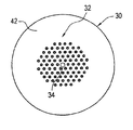
図4を参照すると、本発明の好適な実施例によるフォトニック結晶ファイバ(PCF)30の断面図が示されている。PCF30は、高屈折率のファイバコア領域34の周囲に形成された低屈折率の内側クラッド領域32を含む。しかしながら、ブラッグ散乱の効果を増やすために、僅かに高い屈折率の内側クラッド領域32によって包囲された低屈折率ファイバコア領域34を含むPCF30を製造することが可能である。内側クラッド領域32は、リング構造36の周期格子からなる。PCF30の特定の特徴は、コア領域34がリング構造36を含まないことである。その結果、コア領域32は、格子構造における欠陥として機能して、導波路を通る光をガイドする。ファイバコア領域34は、好ましくは、シリカから形成され、n=約1.45の屈折率(n)を有する。しかしながら、コア領域34は、屈折率特性を交互に変化させるために添加されたシリカから形成されてもよい。外側クラッド領域42は、好ましくは添加されたシリカから形成され、少なくとも内側クラッド領域32の屈折率よりも高い屈折率を有して、内側クラッド領域32を包囲する。具体的には図示されないが、吸収ポリマーコーティングがファイバ30の外表面に与えられる。
Referring to FIG. 4, a cross-sectional view of a photonic crystal fiber (PCF) 30 according to a preferred embodiment of the present invention is shown. The
図5に関して、各々のリング構造36は、内部コア40を包囲する環状リング38によって画定される。各々の環状リング38は、低屈折率ガラスのような固体(中実)材料の環状カラムによって形成されることが好ましい。好ましくは、各々の内部コア40は、環状リング38の屈折率未満の屈折率を有する。各内部コア40に好適な組成は、空気又は低屈折率材料、例えばフッ素又はチタンを添加したシリカである。しかしながら、当業者は様々な材料が内部コア40の格子のために使用され得ることを認識するであろう。環状リング38の材料は、リング38を包囲する材料よりも高い温度でより安定なリングとなるように選択され得る。認識されるように、この特徴は、内部コア40が空気のカラムであるとき、各環状リング38をその形状に維持することを補助して、溶融スプライシング又はテーパリングの間での各内部コア40の圧壊を防止する。
With reference to FIG. 5, each
環状リング構造36の結果として生じる周期格子は、ファイバコア領域34よりも低い屈折率を有する内側クラッド領域32を生じる。これは、環状リング38を形成している材料がファイバコア領域34を形成しているシリカ又は添加されたシリカ材料未満の平均屈折率を生じる理由である。コアとクラッドの間の屈折率の差は、しばしば屈折率デルタと称される。図示されるように、内側クラッド領域32は、リング構造36の三角形の格子である。しかしながら、当業者は、四角形又は他の適切な構造を含むが、これに限定されることなく、リング構造36が様々な構造にアレンジされ得ることを認識するであろう。
The resulting periodic grating of the
ここで、図6に戻って、本発明の他の好適な実施例による内側クラッド領域44の部分断面図が示される。内側クラッド領域44は、内側クラッド領域32についてPCF30(図4)と置換されてもよい。内側クラッド領域44は、セル状リング構造46をモディファイした屈折率の三角形格子としても図示される。セル状リング構造46をモディファイした各屈折率は、コアを囲む屈折率モディファイ殻を形成する複数のカラム構造50によって包囲された内部コア48を含む。図示するように、6つのカラム50は、各内部コア48の周囲にセル状リングを形成する。カラム50は、好ましくは、ファイバ30に沿って空気カラムを形成するボイドである。あるいは、カラム50は、カラム50又はファイバコア領域34を包囲する外側クラッド領域の基板シリカとは異なる固体材料であることが好ましい。好ましくは、各内部コア48は、低屈折率材料、例えばフッ素又はチタンを添加されたシリカから形成される。好適な組み合わせにおいて、各内部コア48は、外側クラッド領域42の周囲のシリカ基板よりも低い屈折率を有する材料である。しばしば、より低い屈折率を有する当該材料を、マイナスのデルタ材料と称する。
Returning now to FIG. 6, a partial cross-sectional view of the
図7は、ファイバ30が溶融スプライス若しくはテーパー付けされた後のクラッド領域44を示す。より具体的には、スプライシング又はテーパリング工程によって、内部コア48の格子を残して、収縮若しくは完全に圧壊して、セル状リング構造46が生じる。圧壊されたリング構造は、52として一般に図示される。セル状リング構造46を形成する空気リング又はカラム50が圧壊するときに、圧壊領域の範囲内の屈折率コントラストは、セル状リング構造46が損なわれていないそれらの領域ほど高くないであろう。-0.5%のデルタであっても、ショートスプライス又はテーパー距離に亘って光をガイドするだろうことを実験は示している。
FIG. 7 shows the
内側クラッド領域32若しくは44のいずれかを有する結果として生じるファイバ30は、以下の動作特性を有する。短波長では、モードは実質的に環状リング構造36又はセル状リング構造46から締め出され、これらのクラッド領域のいずれかを有する導波路ファイバ30は実質的に同じ動作をなす。より長い波長では、モードはリング構造の外径によるファイバ特性の変化を生じさせる環状リング構造36又はセル状リング構造46を通過する。
The resulting
実験工程の一部として、環状リング構造36及びセル状リング構造46は、平面波展開(PWE)コンピューターコードを使用してモデル化された。図8は、半径を変化させた環状リング38を含む構造でのスケールフリーの空間波長の逆数の関数として、実効V値(Veff)のコンピュータ計算された変化を示す。
As part of the experimental process,
参照破線54は、例えば、図2に示されるPCF16の如き、典型的な多孔質クラッド光ファイバでの波長の逆数スケールの関数としてVeffを表したものである。図4及び5について上記した如く、多孔質クラッド層18は、環状リング構造36の周期格子と置換された。図8において、Λ(ラムダ)は、環状リング構造36の間の中心と中心の間隔である。破線54では、空気カラム20の各々は、半径r=0.25Λを有する。他の実線56、58、60、62及び64は、それぞれ、Δr=0.01Λ、Δr=0.02Λ、Δr=0.03Λ、Δr=0.04Λ及びΔr=0.05Λのリング厚さを有する環状リング38を表す。
Reference broken
図8のグラフィックデータから、短波長では曲線が同一になることが明らかになる。しかしながら、長波長では曲線は異なり、クラッド領域32を有する光ファイバの間で僅かに異なる特性が環状リング構造36から形成されることを示す。より小さな半径の環状リング38であっても、モードは閉じ込まれたままである。しかしながら、より短波長では、かかる構造は、より低い開口数(NA)を有し、曲げ損失に対してより影響されやすくなるであろう。
From the graphic data of FIG. 8, it is clear that the curves are the same at short wavelengths. However, at longer wavelengths, the curves are different, indicating that slightly different characteristics are formed from the
図9は、図6に示される構造でのVeffの計算された変化のグラフである。再度、参照破線54は、例えば、図2に示されるPCF16の如き、典型的な多孔質クラッド光ファイバでの波長の逆数スケールの関数としてVeffを表したものである。図6において上記した如く、多孔質クラッド層18は、セル状リング構造46の周期格子と置換されてきた。図9において、Λ(ラムダ)は、セル状リング構造46の間の中心と中心の間隔である。破線54では、空気カラム20の各々は、上記した如く、r=0.25Λの半径を有する。その他の点線66及び実線68は、6つの小さいカラムの各々50が半径r=0.0518Λを有するセル状リング構造46を表す。また、各カラム50の中央は、半径r=0.198Λの円内に分布している。破線54と比較すると、6つのカラムの各グループ50は、r=0.25Λの外周の円内に含まれる。好ましくは6つのカラムであるが、3つ以上のカラムの構造50は、同様の結果を生じることが示された。更に、点線66は、0.5%のフッ素を添加したシリカから形成された内部コア48を有するセル状リング構造46を表す。実線68は、シリカから形成される内部コア48を有するセル状リング構造46を表す。更に、特性は、短波長では空気カラム20とほぼ同一であるが、長波長では異なる。
FIG. 9 is a graph of the calculated change in Veff for the structure shown in FIG. Again, the reference dashed
上記したように、図2、5及び6の光ファイバ構造は、2つの方向に周期的であって且つファイバの長さ方向に沿って均一な二次元フォトニック結晶を形成する。図2、5及び6の構造において、フォトニックバンドギャップは、ファイバに沿っての伝搬に対して現れる。これらの構造のいずれかのコア領域34は、周期構造中に欠陥を生成するために高屈折率又は低屈折率であり得る。光がコア領域34を形成する欠陥に導かれるとき、バンドギャップによって定義される周波数範囲内の光周波数が欠陥に沿って反射される。周期性平面内での光伝搬のために、光モードは、各々独自のバンド構造を有する2つの独立した偏光に分割され得る。
As described above, the optical fiber structure of FIGS. 2, 5 and 6 forms a two-dimensional photonic crystal that is periodic in two directions and uniform along the length of the fiber. In the structures of FIGS. 2, 5 and 6, a photonic band gap appears for propagation along the fiber. The
これらのバンドギャップの例として、図10は、図1に示される構造の中にあるXY平面内を伝搬する光のフォトニックバンド図を示す。図10のプロットでは、図1における構造の高屈折率シリンダ12は、固体である。
As an example of these band gaps, FIG. 10 shows a photonic band diagram of light propagating in the XY plane in the structure shown in FIG. In the plot of FIG. 10, the
図10は、横磁界(TM)モードでのフォトニックバンドギャップがそれぞれ第1及び第2のバンドを表す実線70及び72の間に存在することを示している。実線又はその束はTMモードを表し、点線又はその束は横電界(TE)モードを表す。すなわち、固体シリンダ構造12によって形成されるフォトニック結晶10は、第1及び第2のバンド間にあるTMモードに対して完全なバンドギャップを有するがTEモードでは有しない。
FIG. 10 shows that a photonic band gap in transverse magnetic field (TM) mode exists between
同様に、図11は、固体カラム12が高屈折率環状リングによって置換された図1のフォトニック結晶構造におけるバンドダイアグラムを示す。
Similarly, FIG. 11 shows a band diagram in the photonic crystal structure of FIG. 1 in which the
図11も、横磁界(TM)モードでのフォトニックバンドギャップが第1及び第2のバンドのそれぞれを表す実線74及び76の間に存在することを示す。すなわち、環状リング構造によって形成されるフォトニック結晶構造10は、第1及び第2のバンド間でTMモードに対して完全なバンドギャップを有するがTEモードでは有しない。
FIG. 11 also shows that a photonic band gap in transverse magnetic field (TM) mode exists between
上述の議論は、本発明の典型的な実施例を開示及び記載したものである。当業者であれば、さまざまな変更、改良及びバリエーションが特許請求の範囲において定義された本発明の精神と範囲から逸脱することなくなされ得ることを当該議論及び添付の図面、特許請求の範囲から直ちに認識するであろう。 The above discussion discloses and describes exemplary embodiments of the present invention. Those skilled in the art will readily appreciate from the discussion and accompanying drawings and claims that various changes, modifications, and variations may be made without departing from the spirit and scope of the invention as defined in the claims. You will recognize.
Claims (4)
前記クラッド領域は、内側クラッド領域及び外側クラッド領域を含み、前記内側クラッド領域は、リング構造の周期的格子を有し、
前記コア領域が前記リング構造の前記周期的格子の欠陥として機能して前記ファイバ光導波路内で光をガイドし、
前記ファイバ光導波路は所定のモードにおいて光学バンドギャップを有し、
前記リング構造の前記周期的格子は、セル状リング構造の格子であることを特徴とする導波路。 A fiber optical waveguide comprising a core region and a cladding region surrounding the core region,
The cladding region includes an inner cladding region and an outer cladding region, and the inner cladding region has a periodic grating of a ring structure,
The core region functions as a defect of the periodic grating of the ring structure to guide light in the fiber optical waveguide;
The fiber optical waveguide has an optical band gap in a predetermined mode;
The waveguide according to claim 1, wherein the periodic grating of the ring structure is a grating of a cellular ring structure.
Applications Claiming Priority (2)
| Application Number | Priority Date | Filing Date | Title |
|---|---|---|---|
| US09/426,835 US6334017B1 (en) | 1999-10-26 | 1999-10-26 | Ring photonic crystal fibers |
| US09/426,835 | 1999-10-26 |
Related Parent Applications (1)
| Application Number | Title | Priority Date | Filing Date |
|---|---|---|---|
| JP2001533455A Division JP2003513300A (en) | 1999-10-26 | 2000-09-15 | Ring photonic crystal fiber |
Publications (1)
| Publication Number | Publication Date |
|---|---|
| JP2012068646A true JP2012068646A (en) | 2012-04-05 |
Family
ID=23692405
Family Applications (2)
| Application Number | Title | Priority Date | Filing Date |
|---|---|---|---|
| JP2001533455A Pending JP2003513300A (en) | 1999-10-26 | 2000-09-15 | Ring photonic crystal fiber |
| JP2011227800A Ceased JP2012068646A (en) | 1999-10-26 | 2011-10-17 | Ring photonic crystal fiber |
Family Applications Before (1)
| Application Number | Title | Priority Date | Filing Date |
|---|---|---|---|
| JP2001533455A Pending JP2003513300A (en) | 1999-10-26 | 2000-09-15 | Ring photonic crystal fiber |
Country Status (13)
| Country | Link |
|---|---|
| US (1) | US6334017B1 (en) |
| EP (1) | EP1261887A4 (en) |
| JP (2) | JP2003513300A (en) |
| KR (1) | KR20020047279A (en) |
| CN (1) | CN1213312C (en) |
| AU (1) | AU7583700A (en) |
| BR (1) | BR0015066A (en) |
| CA (1) | CA2389101A1 (en) |
| MX (1) | MXPA02004154A (en) |
| RU (1) | RU2002113650A (en) |
| TW (1) | TW460718B (en) |
| WO (1) | WO2001031376A1 (en) |
| ZA (1) | ZA200202453B (en) |
Cited By (1)
| Publication number | Priority date | Publication date | Assignee | Title |
|---|---|---|---|---|
| JP2018505438A (en) * | 2014-12-18 | 2018-02-22 | エヌケイティー フォトニクス アクティーゼルスカブNkt Photonics A/S | Photonic crystal fiber, manufacturing method thereof, and supercontinuum light source |
Families Citing this family (72)
| Publication number | Priority date | Publication date | Assignee | Title |
|---|---|---|---|---|
| US6735368B2 (en) * | 1997-05-16 | 2004-05-11 | Mesophotonics Limited | Optical delay device |
| US6788863B2 (en) | 1997-05-16 | 2004-09-07 | Mesophotonics Limited | Optical delay device |
| GB9710062D0 (en) * | 1997-05-16 | 1997-07-09 | British Tech Group | Optical devices and methods of fabrication thereof |
| CA2368789A1 (en) * | 1999-03-30 | 2000-10-12 | Crystal Fibre A/S | Polarisation preserving optical fibre |
| US6363096B1 (en) * | 1999-08-30 | 2002-03-26 | Lucent Technologies Inc. | Article comprising a plastic laser |
| GB9929345D0 (en) * | 1999-12-10 | 2000-02-02 | Univ Bath | Improvements in and related to photonic-crystal fibres and photonic-crystal fibe devices |
| US6718105B2 (en) * | 2000-02-23 | 2004-04-06 | Sumitomo Electric Industries, Ltd. | Optical fiber |
| US6788865B2 (en) * | 2000-03-03 | 2004-09-07 | Nippon Telegraph And Telephone Corporation | Polarization maintaining optical fiber with improved polarization maintaining property |
| US6606440B2 (en) * | 2000-05-15 | 2003-08-12 | Sumitomo Electric Industries, Ltd. | Microstructured optical fiber |
| US6445862B1 (en) * | 2000-06-20 | 2002-09-03 | Corning Incorporated | Dispersion compensating photonic crystal fiber |
| US6792188B2 (en) | 2000-07-21 | 2004-09-14 | Crystal Fibre A/S | Dispersion manipulating fiber |
| US6674949B2 (en) * | 2000-08-15 | 2004-01-06 | Corning Incorporated | Active photonic crystal waveguide device and method |
| AUPQ968800A0 (en) * | 2000-08-25 | 2000-09-21 | University Of Sydney, The | Polymer optical waveguide |
| US6658183B1 (en) * | 2000-10-20 | 2003-12-02 | Lucent Technologies Inc. | Process for fabricating tapered microstructured fiber system and resultant system |
| US20040052485A1 (en) * | 2000-11-21 | 2004-03-18 | Martijn Van Eijkelenborg | Terminating polymer optical fibre |
| AUPR159400A0 (en) * | 2000-11-21 | 2000-12-14 | Redfern Photonics Pty Limited | Terminating optical fibre |
| JP2002214466A (en) * | 2001-01-23 | 2002-07-31 | Sumitomo Electric Ind Ltd | Optical fiber |
| WO2002059656A2 (en) * | 2001-01-25 | 2002-08-01 | Omniguide Communications | Low-loss photonic crystal waveguide having large core radius |
| US6895154B2 (en) * | 2001-01-25 | 2005-05-17 | Omniguide Communications | Photonic crystal optical waveguides having tailored dispersion profiles |
| WO2002061467A2 (en) | 2001-01-31 | 2002-08-08 | Omniguide Communications | Electromagnetic mode conversion in photonic crystal multimode waveguides |
| US6618535B1 (en) * | 2001-04-05 | 2003-09-09 | Nortel Networks Limited | Photonic bandgap device using coupled defects |
| US20020197042A1 (en) * | 2001-04-06 | 2002-12-26 | Shigeo Kittaka | Optical device, and wavelength multiplexing optical recording head |
| WO2002084351A1 (en) * | 2001-04-12 | 2002-10-24 | Omniguide Communications Inc. | High index-contrast fiber waveguides and applications |
| JP3665273B2 (en) * | 2001-05-11 | 2005-06-29 | 株式会社日立製作所 | Chromatic dispersion compensator and optical transmission system using the same |
| KR100390642B1 (en) * | 2001-06-08 | 2003-07-07 | 학교법인 포항공과대학교 | Plastic photonic crystal fiber for terahertz wave transmission and method for manufacturing thereof |
| US7590323B2 (en) * | 2001-08-30 | 2009-09-15 | Crystal Fibre A/S | Optical fibre with high numerical aperture, method of its production, and use thereof |
| WO2003023470A1 (en) * | 2001-09-13 | 2003-03-20 | Technical University Of Denmark | Large-bandwidth photonic crystal waveguides |
| US7266275B2 (en) | 2002-03-15 | 2007-09-04 | Crystal Fibre A/S | Nonlinear optical fibre method of its production and use thereof |
| US6795617B2 (en) * | 2002-05-02 | 2004-09-21 | Lucent Technologies Inc. | Optical device for generating pulsed light |
| JP4137515B2 (en) * | 2002-05-17 | 2008-08-20 | 日本電信電話株式会社 | Dispersion-shifted optical fiber |
| JP2005533287A (en) * | 2002-07-18 | 2005-11-04 | ディーエスエム アイピー アセッツ ビー.ブイ. | Coated photonic crystal fiber |
| KR100428410B1 (en) * | 2002-07-29 | 2004-04-28 | 학교법인 성균관대학 | Photonic crystal optical couplers and Optical switch |
| US20040061863A1 (en) * | 2002-08-20 | 2004-04-01 | Digonnet Michel J.F. | Fiber optic sensors with reduced noise |
| US7738109B2 (en) * | 2002-08-20 | 2010-06-15 | The Board Of Trustees Of The Leland Stanford Junior University | Fiber optic sensor using a Bragg fiber |
| US20040050110A1 (en) * | 2002-08-29 | 2004-03-18 | Berkey George E. | Methods for fabricating optical fibers and optical fiber preforms |
| KR100443680B1 (en) * | 2002-11-01 | 2004-08-11 | 엘지전자 주식회사 | Optical fiber using of photonic bandgap and the method |
| US20040141702A1 (en) | 2002-11-22 | 2004-07-22 | Vladimir Fuflyigin | Dielectric waveguide and method of making the same |
| AU2003281985A1 (en) * | 2002-11-23 | 2004-06-18 | Crystal Fibre A/S | Splicing and connectorization of photonic crystal fibres |
| US7361171B2 (en) | 2003-05-20 | 2008-04-22 | Raydiance, Inc. | Man-portable optical ablation system |
| US8921733B2 (en) | 2003-08-11 | 2014-12-30 | Raydiance, Inc. | Methods and systems for trimming circuits |
| US6993228B2 (en) * | 2003-08-13 | 2006-01-31 | Corning Incorporated | Dispersion compensated optical fiber transmission system and module including micro-structured optical fiber |
| EP1664852B1 (en) * | 2003-09-12 | 2016-12-14 | The Board of Trustees of The Leland Stanford Junior University | Method for configuring air-core photonic-bandgap fibers free of surface modes |
| CN100410704C (en) * | 2003-09-12 | 2008-08-13 | 里兰斯坦福初级大学理事会 | Method of configuring air core photonic bandgap fiber without surface mode and photonic bandgap fiber |
| US7280730B2 (en) | 2004-01-16 | 2007-10-09 | Imra America, Inc. | Large core holey fibers |
| CN101288009B (en) * | 2004-05-08 | 2011-03-23 | 里兰斯坦福初级大学理事会 | Photonic-bandgap fiber with hollow ring |
| US7209619B2 (en) | 2004-12-30 | 2007-04-24 | Imra America, Inc. | Photonic bandgap fibers |
| US7787729B2 (en) | 2005-05-20 | 2010-08-31 | Imra America, Inc. | Single mode propagation in fibers and rods with large leakage channels |
| US7242835B2 (en) * | 2005-07-18 | 2007-07-10 | The United States Of America As Represented By The Secretary Of The Navy | Optical fiber clad-protective terminations |
| CN100378477C (en) * | 2005-09-29 | 2008-04-02 | 武汉理工大学 | A photonic crystal fiber with conductive properties and its preparation method |
| US7394961B2 (en) * | 2005-10-13 | 2008-07-01 | Pavel Kornilovich | Waveguide having low index substrate |
| MXGT05000015A (en) * | 2005-11-15 | 2007-05-14 | Vladimir P Minkovich | Tapered microstructured optical fibre with selective transmission for optical fibre sensors and production method thereof. |
| US8189971B1 (en) | 2006-01-23 | 2012-05-29 | Raydiance, Inc. | Dispersion compensation in a chirped pulse amplification system |
| CA2656420A1 (en) * | 2006-06-29 | 2008-01-03 | The Board Of Trustees Of The Leland Stanford Junior University | Fiber optic sensor using a bragg fiber |
| CN100426023C (en) * | 2006-10-26 | 2008-10-15 | 长飞光纤光缆有限公司 | Full solid band-gap optical fiber with low limited loss and low bending loss |
| RU2397516C2 (en) * | 2007-06-15 | 2010-08-20 | Федеральное государственное унитарное предприятие "Научно-исследовательский и технологический институт оптического материаловедения Всероссийского научного центра "Государственный оптический институт им. С.И. Вавилова" (ФГУП "НИТИОМ ВНЦ "ГОИ им. С.И. Вавилова") | Photon-crystalline electrooptical fibre and method of making said fibre |
| JP5662151B2 (en) * | 2007-09-26 | 2015-01-28 | イムラ アメリカ インコーポレイテッド | Glass large core optical fiber |
| US8378567B2 (en) * | 2007-11-21 | 2013-02-19 | Industrial Technology Research Institute | Light-polarizing structure |
| US20090159310A1 (en) * | 2007-12-19 | 2009-06-25 | Nicholas Francis Borrelli | Photonic-Crystal Transparent-Conductor Assembly |
| GB2457947B (en) * | 2008-02-29 | 2012-10-17 | Sumitomo Electric Industries | All solid photonic bandgap fibre |
| GB2457946B (en) * | 2008-02-29 | 2011-11-16 | Sumitomo Electric Industries | Method of manufacturing photonic bandgap fibre |
| GB2457948B (en) | 2008-02-29 | 2012-01-25 | Sumitomo Electric Industries | Photonic bandgap fibre |
| TW201024800A (en) | 2008-12-30 | 2010-07-01 | Ind Tech Res Inst | Negative refraction photonic crystal lens |
| US7952772B2 (en) * | 2009-05-08 | 2011-05-31 | Honeywell International Inc. | Photonic crystal fiber sensor |
| US20110026870A1 (en) | 2009-07-31 | 2011-02-03 | Honeywell International Inc. | Photonic crystal fiber sensor |
| CN103080796B (en) * | 2010-06-25 | 2016-04-27 | Nkt光子学有限公司 | The single-mode fiber of large core area |
| US8554037B2 (en) | 2010-09-30 | 2013-10-08 | Raydiance, Inc. | Hybrid waveguide device in powerful laser systems |
| US9065245B2 (en) | 2010-11-23 | 2015-06-23 | Fraunhofer-Gesellschaft Zur Foerderung Der Angewandten Forschung E.V. | Structured double-sheath fiber |
| US9007681B2 (en) * | 2011-12-13 | 2015-04-14 | Ofs Fitel, Llc | Multi-core erbium-doped fiber amplifier |
| US9025239B2 (en) * | 2011-12-13 | 2015-05-05 | Ofs Fitel, Llc | Multi-core erbium-doped fiber amplifier |
| CN103760633A (en) * | 2014-01-14 | 2014-04-30 | 中国科学院上海光学精密机械研究所 | Double-cladding all-solid photonic crystal gain fiber and manufacturing method thereof |
| CN104062704B (en) * | 2014-06-13 | 2017-01-11 | 中国科学院西安光学精密机械研究所 | Microstructured optical fiber for generating and transmitting vortex light beam |
| CN104503019B (en) * | 2015-01-09 | 2017-12-12 | 中南民族大学 | Tetragonal slower rays photon band-gap optical fiber |
Citations (4)
| Publication number | Priority date | Publication date | Assignee | Title |
|---|---|---|---|---|
| JPH1095628A (en) * | 1996-05-31 | 1998-04-14 | Lucent Technol Inc | Optical fiber-containing product having fine structure and production of optical fiber having fine structure |
| WO1999000685A1 (en) * | 1997-06-26 | 1999-01-07 | The Secretary Of State For Defence | Single mode optical fibre |
| WO1999064904A1 (en) * | 1998-06-09 | 1999-12-16 | Crystal Fibre A/S | A photonic band gap fibre |
| JP2002537575A (en) * | 1999-02-19 | 2002-11-05 | ブレイズフォトニクス リミティド | Photonic crystal fiber and improvements related thereto |
Family Cites Families (5)
| Publication number | Priority date | Publication date | Assignee | Title |
|---|---|---|---|---|
| US5278931A (en) | 1992-12-31 | 1994-01-11 | Corning Incorporated | Low bend loss singlemode optical waveguide fiber |
| GB2310506B (en) * | 1996-02-22 | 2000-10-25 | Hitachi Cable | Rare earth element-doped multiple-core optical fiber and optical systems using them |
| US5802236A (en) | 1997-02-14 | 1998-09-01 | Lucent Technologies Inc. | Article comprising a micro-structured optical fiber, and method of making such fiber |
| US5907652A (en) | 1997-09-11 | 1999-05-25 | Lucent Technologies Inc. | Article comprising an air-clad optical fiber |
| US6097890A (en) * | 1999-01-21 | 2000-08-01 | Eastman Kodak Company | One-time-use camera with fracture line of weakness non-coincident to pivot axis of film door |
-
1999
- 1999-10-26 US US09/426,835 patent/US6334017B1/en not_active Expired - Lifetime
-
2000
- 2000-09-15 CA CA002389101A patent/CA2389101A1/en not_active Abandoned
- 2000-09-15 RU RU2002113650/28A patent/RU2002113650A/en unknown
- 2000-09-15 KR KR1020027005308A patent/KR20020047279A/en not_active Withdrawn
- 2000-09-15 WO PCT/US2000/025363 patent/WO2001031376A1/en not_active Ceased
- 2000-09-15 CN CNB008147167A patent/CN1213312C/en not_active Expired - Fee Related
- 2000-09-15 EP EP00965051A patent/EP1261887A4/en not_active Withdrawn
- 2000-09-15 JP JP2001533455A patent/JP2003513300A/en active Pending
- 2000-09-15 AU AU75837/00A patent/AU7583700A/en not_active Abandoned
- 2000-09-15 MX MXPA02004154A patent/MXPA02004154A/en unknown
- 2000-09-15 BR BR0015066-5A patent/BR0015066A/en not_active Application Discontinuation
- 2000-10-25 TW TW089122604A patent/TW460718B/en not_active IP Right Cessation
-
2002
- 2002-03-27 ZA ZA200202453A patent/ZA200202453B/en unknown
-
2011
- 2011-10-17 JP JP2011227800A patent/JP2012068646A/en not_active Ceased
Patent Citations (4)
| Publication number | Priority date | Publication date | Assignee | Title |
|---|---|---|---|---|
| JPH1095628A (en) * | 1996-05-31 | 1998-04-14 | Lucent Technol Inc | Optical fiber-containing product having fine structure and production of optical fiber having fine structure |
| WO1999000685A1 (en) * | 1997-06-26 | 1999-01-07 | The Secretary Of State For Defence | Single mode optical fibre |
| WO1999064904A1 (en) * | 1998-06-09 | 1999-12-16 | Crystal Fibre A/S | A photonic band gap fibre |
| JP2002537575A (en) * | 1999-02-19 | 2002-11-05 | ブレイズフォトニクス リミティド | Photonic crystal fiber and improvements related thereto |
Cited By (6)
| Publication number | Priority date | Publication date | Assignee | Title |
|---|---|---|---|---|
| JP2018505438A (en) * | 2014-12-18 | 2018-02-22 | エヌケイティー フォトニクス アクティーゼルスカブNkt Photonics A/S | Photonic crystal fiber, manufacturing method thereof, and supercontinuum light source |
| US10557987B2 (en) | 2014-12-18 | 2020-02-11 | Nkt Photonics A/S | Photonic crystal fiber, a method of production thereof and a supercontinuum light source |
| US10928584B2 (en) | 2014-12-18 | 2021-02-23 | Nkt Photonics A/S | Photonic crystal fiber, a method of production thereof and a supercontinuum light source |
| US11409033B2 (en) | 2014-12-18 | 2022-08-09 | Nkt Photonics A/S | Photonic crystal fiber, a method of production thereof and a supercontinuum light source |
| US11719881B2 (en) | 2014-12-18 | 2023-08-08 | Nkt Photonics A/S | Photonic crystal fiber, a method of production thereof and a supercontinuum light source |
| US12169303B2 (en) | 2014-12-18 | 2024-12-17 | Nkt Photonics A/S | Photonic crystal fiber, a method of production thereof and a supercontinuum light source |
Also Published As
| Publication number | Publication date |
|---|---|
| CN1382265A (en) | 2002-11-27 |
| CA2389101A1 (en) | 2001-05-03 |
| AU7583700A (en) | 2001-05-08 |
| KR20020047279A (en) | 2002-06-21 |
| EP1261887A4 (en) | 2005-09-07 |
| BR0015066A (en) | 2002-06-18 |
| EP1261887A1 (en) | 2002-12-04 |
| CN1213312C (en) | 2005-08-03 |
| WO2001031376A1 (en) | 2001-05-03 |
| US6334017B1 (en) | 2001-12-25 |
| ZA200202453B (en) | 2002-12-24 |
| TW460718B (en) | 2001-10-21 |
| JP2003513300A (en) | 2003-04-08 |
| MXPA02004154A (en) | 2002-10-17 |
| RU2002113650A (en) | 2004-02-10 |
Similar Documents
| Publication | Publication Date | Title |
|---|---|---|
| US6334017B1 (en) | Ring photonic crystal fibers | |
| EP1086391B1 (en) | Microstructured optical fibres | |
| US6418258B1 (en) | Microstructured optical fiber with improved transmission efficiency and durability | |
| US6445862B1 (en) | Dispersion compensating photonic crystal fiber | |
| CA2368778C (en) | A photonic crystal fibre and a method for its production | |
| US6788865B2 (en) | Polarization maintaining optical fiber with improved polarization maintaining property | |
| US7376307B2 (en) | Multimode long period fiber bragg grating machined by ultrafast laser direct writing | |
| US7046887B2 (en) | Polarization preserving optical fiber and absolute single polarization optical fiber | |
| JP5679420B2 (en) | Solid photonic bandgap fiber, fiber module and fiber amplifier using the fiber, and fiber laser | |
| CN106575012A (en) | hollow core fiber | |
| EP1745316A1 (en) | Microstructured optical fibre | |
| GB2350904A (en) | A photonic crystal fibre and its production | |
| EP1468316A1 (en) | Ring structures in optical fibres | |
| US11796734B2 (en) | 3D printed waveguides and method based on photonic crystal fibers | |
| WO2001037008A2 (en) | Photonic crystal fibers with high resistance to bend loss | |
| Sufian et al. | Light transmission through a hollow core fiber bundle | |
| Seraji et al. | A review on the designed low–loss single–mode optical fiber used in fiber–to–the–home networks | |
| Bartelt | Micro-and nanostructured optical fibres |
Legal Events
| Date | Code | Title | Description |
|---|---|---|---|
| A977 | Report on retrieval |
Free format text: JAPANESE INTERMEDIATE CODE: A971007 Effective date: 20130410 |
|
| A01 | Written decision to grant a patent or to grant a registration (utility model) |
Free format text: JAPANESE INTERMEDIATE CODE: A01 Effective date: 20130423 |
|
| A045 | Written measure of dismissal of application [lapsed due to lack of payment] |
Free format text: JAPANESE INTERMEDIATE CODE: A045 Effective date: 20130827 |