JP2011254078A - Semiconductor die, light-emitting device, method of manufacturing the same, and method of generating multiple-wavelength light - Google Patents
Semiconductor die, light-emitting device, method of manufacturing the same, and method of generating multiple-wavelength light Download PDFInfo
- Publication number
- JP2011254078A JP2011254078A JP2011121587A JP2011121587A JP2011254078A JP 2011254078 A JP2011254078 A JP 2011254078A JP 2011121587 A JP2011121587 A JP 2011121587A JP 2011121587 A JP2011121587 A JP 2011121587A JP 2011254078 A JP2011254078 A JP 2011254078A
- Authority
- JP
- Japan
- Prior art keywords
- light emitting
- semiconductor die
- emitting structures
- wavelength
- nitride semiconductor
- Prior art date
- Legal status (The legal status is an assumption and is not a legal conclusion. Google has not performed a legal analysis and makes no representation as to the accuracy of the status listed.)
- Pending
Links
Images


Classifications
-
- H—ELECTRICITY
- H10—SEMICONDUCTOR DEVICES; ELECTRIC SOLID-STATE DEVICES NOT OTHERWISE PROVIDED FOR
- H10H—INORGANIC LIGHT-EMITTING SEMICONDUCTOR DEVICES HAVING POTENTIAL BARRIERS
- H10H20/00—Individual inorganic light-emitting semiconductor devices having potential barriers, e.g. light-emitting diodes [LED]
- H10H20/80—Constructional details
- H10H20/81—Bodies
- H10H20/813—Bodies having a plurality of light-emitting regions, e.g. multi-junction LEDs or light-emitting devices having photoluminescent regions within the bodies
-
- B—PERFORMING OPERATIONS; TRANSPORTING
- B82—NANOTECHNOLOGY
- B82Y—SPECIFIC USES OR APPLICATIONS OF NANOSTRUCTURES; MEASUREMENT OR ANALYSIS OF NANOSTRUCTURES; MANUFACTURE OR TREATMENT OF NANOSTRUCTURES
- B82Y20/00—Nanooptics, e.g. quantum optics or photonic crystals
-
- B—PERFORMING OPERATIONS; TRANSPORTING
- B82—NANOTECHNOLOGY
- B82Y—SPECIFIC USES OR APPLICATIONS OF NANOSTRUCTURES; MEASUREMENT OR ANALYSIS OF NANOSTRUCTURES; MANUFACTURE OR TREATMENT OF NANOSTRUCTURES
- B82Y30/00—Nanotechnology for materials or surface science, e.g. nanocomposites
-
- H—ELECTRICITY
- H10—SEMICONDUCTOR DEVICES; ELECTRIC SOLID-STATE DEVICES NOT OTHERWISE PROVIDED FOR
- H10H—INORGANIC LIGHT-EMITTING SEMICONDUCTOR DEVICES HAVING POTENTIAL BARRIERS
- H10H20/00—Individual inorganic light-emitting semiconductor devices having potential barriers, e.g. light-emitting diodes [LED]
- H10H20/80—Constructional details
- H10H20/81—Bodies
- H10H20/811—Bodies having quantum effect structures or superlattices, e.g. tunnel junctions
- H10H20/812—Bodies having quantum effect structures or superlattices, e.g. tunnel junctions within the light-emitting regions, e.g. having quantum confinement structures
-
- H—ELECTRICITY
- H10—SEMICONDUCTOR DEVICES; ELECTRIC SOLID-STATE DEVICES NOT OTHERWISE PROVIDED FOR
- H10H—INORGANIC LIGHT-EMITTING SEMICONDUCTOR DEVICES HAVING POTENTIAL BARRIERS
- H10H20/00—Individual inorganic light-emitting semiconductor devices having potential barriers, e.g. light-emitting diodes [LED]
- H10H20/80—Constructional details
- H10H20/81—Bodies
- H10H20/817—Bodies characterised by the crystal structures or orientations, e.g. polycrystalline, amorphous or porous
- H10H20/818—Bodies characterised by the crystal structures or orientations, e.g. polycrystalline, amorphous or porous within the light-emitting regions
-
- H—ELECTRICITY
- H10—SEMICONDUCTOR DEVICES; ELECTRIC SOLID-STATE DEVICES NOT OTHERWISE PROVIDED FOR
- H10H—INORGANIC LIGHT-EMITTING SEMICONDUCTOR DEVICES HAVING POTENTIAL BARRIERS
- H10H20/00—Individual inorganic light-emitting semiconductor devices having potential barriers, e.g. light-emitting diodes [LED]
- H10H20/80—Constructional details
- H10H20/81—Bodies
- H10H20/819—Bodies characterised by their shape, e.g. curved or truncated substrates
- H10H20/821—Bodies characterised by their shape, e.g. curved or truncated substrates of the light-emitting regions, e.g. non-planar junctions
-
- H—ELECTRICITY
- H10—SEMICONDUCTOR DEVICES; ELECTRIC SOLID-STATE DEVICES NOT OTHERWISE PROVIDED FOR
- H10H—INORGANIC LIGHT-EMITTING SEMICONDUCTOR DEVICES HAVING POTENTIAL BARRIERS
- H10H20/00—Individual inorganic light-emitting semiconductor devices having potential barriers, e.g. light-emitting diodes [LED]
- H10H20/80—Constructional details
- H10H20/81—Bodies
- H10H20/822—Materials of the light-emitting regions
- H10H20/824—Materials of the light-emitting regions comprising only Group III-V materials, e.g. GaP
- H10H20/825—Materials of the light-emitting regions comprising only Group III-V materials, e.g. GaP containing nitrogen, e.g. GaN
Landscapes
- Chemical & Material Sciences (AREA)
- Engineering & Computer Science (AREA)
- Nanotechnology (AREA)
- Physics & Mathematics (AREA)
- Crystallography & Structural Chemistry (AREA)
- Materials Engineering (AREA)
- General Physics & Mathematics (AREA)
- Condensed Matter Physics & Semiconductors (AREA)
- Composite Materials (AREA)
- Life Sciences & Earth Sciences (AREA)
- Biophysics (AREA)
- Optics & Photonics (AREA)
- Led Devices (AREA)
- Led Device Packages (AREA)
- Semiconductor Lasers (AREA)
Abstract
【課題】より長い波長の発光効率を上昇させることが可能な半導体ダイ、発光デバイス、製造する方法および多波長光を生成する方法を提供する。
【解決手段】半導体ダイは、少なくとも1つの第1の領域と少なくとも1つの第2の領域とを含む。少なくとも1つの第1の領域は、少なくとも第1の波長を有する光を発光するように構成される。少なくとも1つの第2の領域は、少なくとも第2の波長を有する光を発光するように構成され、この第2の波長は、第1の波長とは異なる。
【選択図】図5A semiconductor die, a light-emitting device, a manufacturing method, and a method for generating multi-wavelength light capable of increasing light emission efficiency at a longer wavelength are provided.
The semiconductor die includes at least one first region and at least one second region. The at least one first region is configured to emit light having at least a first wavelength. The at least one second region is configured to emit light having at least a second wavelength, the second wavelength being different from the first wavelength.
[Selection] Figure 5
Description
例示的な実施形態は、半導体ダイ、発光デバイス(LED)、製造する方法および多波長光を生成する方法に関する。 Exemplary embodiments relate to semiconductor dies, light emitting devices (LEDs), methods of manufacturing, and methods of generating multi-wavelength light.
発光デバイス(LED)は、比較的効率的かつ環境に優しい光源である。LEDは、ディスプレイ、光通信、自動車、および一般的な照明などの様々な分野で使用されている。 Light emitting devices (LEDs) are relatively efficient and environmentally friendly light sources. LEDs are used in various fields such as displays, optical communications, automobiles, and general lighting.
従来のLEDは、白色光を生成するために、蛍光材料を使用する。ある例では、白色光を得るための赤色、緑色および青色の光を発光するために、赤色、緑色および青色の蛍光材料を紫外(UV)線で励起することにより、白色光が得られる。黄色光は、白色光を得るための光源として使用される青色LEDに相補的である黄色蛍光材料を励起することにより発光される。 Conventional LEDs use a fluorescent material to generate white light. In one example, white light is obtained by exciting red, green and blue fluorescent materials with ultraviolet (UV) radiation to emit red, green and blue light to obtain white light. Yellow light is emitted by exciting a yellow fluorescent material that is complementary to a blue LED used as a light source to obtain white light.
従来から、白色光は、蛍光材料を有さないLEDを使用して生成され得る。ある例では、複数のLEDのそれぞれが、赤色、緑色、および青色の可視光の1つを発光し、それらは、白色光を生成するために、組み合わせて使用される。例えば、発光材料として窒化インジウムガリウム(InGaN)層を有するLEDは、発光される色が、InGaN層内のインジウム(In)のモル比率の変化に従って変動するという事実を利用する。しかしながら、インジウム(In)の含有量が増加するにつれて、格子定数が増加し、それは、比較的薄いInGaN層とベース基板との間の比較的大きな格子不整合という結果になる。したがって、発光効率は、比較的短い波長から比較的長い波長まで悪化する場合がある。 Conventionally, white light can be generated using LEDs that do not have a fluorescent material. In one example, each of the plurality of LEDs emits one of red, green, and blue visible light, which are used in combination to generate white light. For example, an LED having an indium gallium nitride (InGaN) layer as a light emitting material takes advantage of the fact that the emitted color varies with changes in the molar ratio of indium (In) in the InGaN layer. However, as the indium (In) content increases, the lattice constant increases, which results in a relatively large lattice mismatch between the relatively thin InGaN layer and the base substrate. Therefore, the luminous efficiency may deteriorate from a relatively short wavelength to a relatively long wavelength.
例示的な実施形態は、比較的長い波長の光の、向上した輝度効率を有する発光デバイス(LED)を提供する。 Exemplary embodiments provide light emitting devices (LEDs) with improved luminance efficiency for relatively long wavelength light.
例示的な実施形態はさらに、蛍光材料を使用することなしに多波長光を発光するように構成される半導体ダイ、およびそれらを含むLEDを提供する。 Exemplary embodiments further provide semiconductor dies configured to emit multi-wavelength light without the use of fluorescent materials, and LEDs including them.
例示的な実施形態はさらに、半導体ダイを製造する方法を提供する。 The illustrative embodiments further provide a method of manufacturing a semiconductor die.
例示的な実施形態はさらに、蛍光材料を使用することなしに多波長光を生成する方法を提供する。 Exemplary embodiments further provide a method of generating multi-wavelength light without using fluorescent materials.
さらなる態様が、部分的には以下の説明で示されることになり、部分的には、説明から明らかとなり、または、例示的な実施形態の実施により知られる場合がある。 Further aspects will be set forth in part in the following description, and in part will be apparent from the description, or may be known by implementation of the exemplary embodiments.
少なくとも1つの例示的な実施形態は、少なくとも第1の波長を有する光を発光するように構成される、少なくとも1つの第1の領域を含む半導体ダイを提供する。少なくとも1つの第1の領域は、複数の第1の発光構造を含み、この複数の第1の発光構造は、複数の第1の発光構造のうちの隣接するもののベースの間に第1のギャップを伴って配置される。半導体ダイはさらに、平坦面および複数の第2の発光構造のうちの1つを有する、少なくとも1つの第2の領域を含む。平坦面は、複数の第1の発光構造の突出方向に垂直であり、複数の第2の発光構造は、相互に隣接して配置される。少なくとも1つの第2の領域は、少なくとも第2の波長を有する光を発光するように構成され、この第2の波長は、第1の波長とは異なる。 At least one exemplary embodiment provides a semiconductor die that includes at least one first region configured to emit light having at least a first wavelength. The at least one first region includes a plurality of first light emitting structures, the plurality of first light emitting structures including a first gap between the bases of adjacent ones of the plurality of first light emitting structures. It is arranged with. The semiconductor die further includes at least one second region having a flat surface and one of a plurality of second light emitting structures. The flat surface is perpendicular to the protruding direction of the plurality of first light emitting structures, and the plurality of second light emitting structures are disposed adjacent to each other. The at least one second region is configured to emit light having at least a second wavelength, the second wavelength being different from the first wavelength.
少なくとも一部の例示的な実施形態によれば、複数の第2の発光構造は、複数の第2の発光構造のうちの隣接するもののベースの間のギャップなしに、相互に隣接して配置される場合がある。複数の第1の発光構造は、多角錐の形状を有する場合がある。誘電層部が、それぞれの第1のギャップに配設される場合がある。誘電層部は、複数の第1の発光構造により覆われない場合がある。複数の第1の発光構造のそれぞれは、複数の半極性面を有する場合がある。 According to at least some example embodiments, the plurality of second light emitting structures are disposed adjacent to each other without a gap between the bases of adjacent ones of the plurality of second light emitting structures. There is a case. The plurality of first light emitting structures may have a polygonal pyramid shape. In some cases, the dielectric layer portion is disposed in each first gap. The dielectric layer portion may not be covered with the plurality of first light emitting structures. Each of the plurality of first light emitting structures may have a plurality of semipolar surfaces.
少なくとも一部の例示的な実施形態によれば、少なくとも1つの第1の領域および少なくとも1つの第2の領域は、第1の窒化物半導体層上に形成される場合がある。複数の第1の発光構造のそれぞれは、第1の窒化物半導体層と同じ材料で形成されるベース部と、ベース部上に形成される第1の活性層と、第1の活性層上に形成される第2の窒化物半導体層とを含む場合がある。 According to at least some example embodiments, the at least one first region and the at least one second region may be formed on the first nitride semiconductor layer. Each of the plurality of first light emitting structures includes a base portion made of the same material as the first nitride semiconductor layer, a first active layer formed on the base portion, and a first active layer And a second nitride semiconductor layer to be formed.
少なくとも一部の例示的な実施形態によれば、複数の多層構造が、複数の第1の発光構造の間に配設される場合がある。複数の多層構造のそれぞれは、第2の活性層と、第2の活性層上に形成される第3の窒化物半導体層と、平坦面または非極性面とを含む場合がある。多層構造は、第2の波長を有する光を発光する場合があり、第1の波長は、第2の波長より長い場合がある。 According to at least some example embodiments, a plurality of multilayer structures may be disposed between the plurality of first light emitting structures. Each of the multiple multilayer structures may include a second active layer, a third nitride semiconductor layer formed on the second active layer, and a flat surface or a nonpolar surface. The multilayer structure may emit light having a second wavelength, and the first wavelength may be longer than the second wavelength.
少なくとも一部の例示的な実施形態によれば、複数の第1の領域および複数の第2の領域が、交互に基板上に配置される場合がある。複数の第1の領域および複数の第2の領域は、発光アレイを形成するように配置される場合がある。 According to at least some example embodiments, the plurality of first regions and the plurality of second regions may be alternately disposed on the substrate. The plurality of first regions and the plurality of second regions may be arranged to form a light emitting array.
少なくとも1つの第2の領域は、第1の幅を有する平坦面を含む場合があり、第1の幅は、第1のギャップの幅より大きい場合がある。 The at least one second region may include a flat surface having a first width, and the first width may be greater than the width of the first gap.
少なくとも一部の例示的な実施形態によれば、少なくとも1つの第2の領域は、複数の第2の発光構造を含む場合があり、少なくとも1つの第1の領域は、少なくとも1つの第2の領域から、第2のギャップだけ隔てられる場合がある。第1のギャップの幅は、第2のギャップの幅と同じ、または実質的に同じである場合がある。 According to at least some example embodiments, the at least one second region may include a plurality of second light emitting structures, and the at least one first region includes at least one second region. The region may be separated by a second gap. The width of the first gap may be the same as or substantially the same as the width of the second gap.
複数の第1の発光構造および複数の第2の発光構造は、ナノサイズの発光構造である場合がある。 The plurality of first light emitting structures and the plurality of second light emitting structures may be nano-sized light emitting structures.
少なくとも1つの他の例示的な実施形態は、少なくとも1つの半導体ダイを含む発光デバイス(LED)を提供する。少なくとも1つの半導体ダイは、少なくとも第1の波長を有する光を発光するように構成される、少なくとも1つの第1の領域を含む。少なくとも1つの第1の領域は、複数の第1の発光構造を含み、この複数の第1の発光構造は、複数の第1の発光構造のうちの隣接するもののベースの間に第1のギャップを伴って配置される。少なくとも1つの半導体ダイはさらに、平坦面および複数の第2の発光構造のうちの1つを有する、少なくとも1つの第2の領域を含む。平坦面は、複数の第1の発光構造の突出方向に垂直であり、複数の第2の発光構造は、相互に隣接して配置される。少なくとも1つの第2の領域は、少なくとも第2の波長を有する光を発光するように構成され、この第2の波長は、第1の波長とは異なる。 At least one other exemplary embodiment provides a light emitting device (LED) that includes at least one semiconductor die. The at least one semiconductor die includes at least one first region configured to emit light having at least a first wavelength. The at least one first region includes a plurality of first light emitting structures, the plurality of first light emitting structures including a first gap between the bases of adjacent ones of the plurality of first light emitting structures. It is arranged with. The at least one semiconductor die further includes at least one second region having a flat surface and one of a plurality of second light emitting structures. The flat surface is perpendicular to the protruding direction of the plurality of first light emitting structures, and the plurality of second light emitting structures are disposed adjacent to each other. The at least one second region is configured to emit light having at least a second wavelength, the second wavelength being different from the first wavelength.
少なくとも一部の例示的な実施形態によれば、LEDは、サーマルヒートシンク(thermal heat sink)と、サーマルヒートシンク上に配置されるシリコンサブマウントであって、少なくとも1つの半導体ダイが上に配置されるシリコンサブマウントと、シリコンサブマウントに結合されるアノードリードおよびカソードリードと、サーマルヒートシンクを囲む外部パッケージと、シリコンサブマウントおよび少なくとも1つの半導体ダイを囲むレンズとをさらに含む場合がある。 According to at least some example embodiments, the LED is a thermal heat sink and a silicon submount disposed on the thermal heat sink with at least one semiconductor die disposed thereon. The silicon submount may further include an anode lead and a cathode lead coupled to the silicon submount, an external package surrounding the thermal heat sink, and a lens surrounding the silicon submount and at least one semiconductor die.
少なくとも1つの他の例示的な実施形態は、少なくとも1つの第1の領域と少なくとも1つの第2の領域とを含む半導体ダイを提供する。少なくとも1つの第1の領域は、第1の波長を有する光を発光するように構成される複数の第1の発光構造を含む。複数の第1の発光構造は、複数の第1の発光構造のうちの隣接するもののベースの間に第1のギャップを伴って配置される。少なくとも1つの第2の領域は、第2の波長を有する光を発光するように構成される複数の第2の発光構造を含む。複数の第2の発光構造は、複数の第2の発光構造のうちの隣接するもののベースの間に第2のギャップを伴って配置される。第2のギャップの幅は、第1のギャップの幅とは異なり、第1の波長は、第2の波長とは異なる。 At least one other exemplary embodiment provides a semiconductor die that includes at least one first region and at least one second region. The at least one first region includes a plurality of first light emitting structures configured to emit light having a first wavelength. The plurality of first light emitting structures are arranged with a first gap between the bases of adjacent ones of the plurality of first light emitting structures. The at least one second region includes a plurality of second light emitting structures configured to emit light having a second wavelength. The plurality of second light emitting structures are disposed with a second gap between the bases of adjacent ones of the plurality of second light emitting structures. The width of the second gap is different from the width of the first gap, and the first wavelength is different from the second wavelength.
少なくとも一部の例示的な実施形態によれば、誘電層が、第1および第2のギャップのそれぞれに配設される場合がある。 According to at least some example embodiments, a dielectric layer may be disposed in each of the first and second gaps.
少なくとも一部の例示的な実施形態によれば、半導体ダイは、少なくとも1つの第3の領域をさらに含む場合がある。少なくとも1つの第3の領域は、第3の波長を有する光を発光するように構成される複数の第3の発光構造を含む場合がある。複数の第3の発光構造は、複数の第1の発光構造のうちの隣接するもののベースの間に第3のギャップを伴って配置される場合がある。第3のギャップの幅は、第1および第2のギャップの幅とは異なる場合があり、第3の波長は、第1および第2の波長とは異なる場合がある。複数の第1の発光構造、複数の第2の発光構造、および複数の第3の発光構造は、同じサイズである場合がある。誘電層が、第1、第2および第3のギャップのそれぞれに配設される場合がある。 According to at least some example embodiments, the semiconductor die may further include at least one third region. The at least one third region may include a plurality of third light emitting structures configured to emit light having a third wavelength. The plurality of third light emitting structures may be arranged with a third gap between the bases of adjacent ones of the plurality of first light emitting structures. The width of the third gap may be different from the width of the first and second gaps, and the third wavelength may be different from the first and second wavelengths. The plurality of first light emitting structures, the plurality of second light emitting structures, and the plurality of third light emitting structures may be the same size. A dielectric layer may be disposed in each of the first, second, and third gaps.
少なくとも一部の例示的な実施形態によれば、複数の第1の発光構造および複数の第2の発光構造は、ナノサイズである場合がある。 According to at least some example embodiments, the plurality of first light emitting structures and the plurality of second light emitting structures may be nano-sized.
複数の第1の発光構造および複数の第2の発光構造は、同じ、または実質的に同じサイズである場合がある。 The plurality of first light emitting structures and the plurality of second light emitting structures may be the same or substantially the same size.
少なくとも一部の例示的な実施形態によれば、少なくとも1つの第1の領域および少なくとも1つの第2の領域は、第1の窒化物半導体層上に形成される場合がある。複数の第1の発光構造および複数の第2の発光構造のそれぞれは、第1の窒化物半導体層と同じ材料で形成されるベース部と、ベース部上に形成される第1の活性層と、第1の活性層上に形成される第2の窒化物半導体層とを含む場合がある。 According to at least some example embodiments, the at least one first region and the at least one second region may be formed on the first nitride semiconductor layer. Each of the plurality of first light emitting structures and the plurality of second light emitting structures includes a base portion formed of the same material as the first nitride semiconductor layer, and a first active layer formed on the base portion. And a second nitride semiconductor layer formed on the first active layer.
少なくとも1つの他の例示的な実施形態は、少なくとも1つの半導体ダイを含むLEDを提供する。少なくとも1つの半導体ダイは、少なくとも1つの第1の領域と少なくとも1つの第2の領域とを含む。少なくとも1つの第1の領域は、第1の波長を有する光を発光するように構成される複数の第1の発光構造を含む。複数の第1の発光構造は、複数の第1の発光構造のうちの隣接するもののベースの間に第1のギャップを伴って配置される。少なくとも1つの第2の領域は、第2の波長を有する光を発光するように構成される複数の第2の発光構造を含む。複数の第2の発光構造は、複数の第2の発光構造のうちの隣接するもののベースの間に第2のギャップを伴って配置される。第2のギャップの幅は、第1のギャップの幅とは異なり、第1の波長は、第2の波長とは異なる。 At least one other exemplary embodiment provides an LED that includes at least one semiconductor die. The at least one semiconductor die includes at least one first region and at least one second region. The at least one first region includes a plurality of first light emitting structures configured to emit light having a first wavelength. The plurality of first light emitting structures are arranged with a first gap between the bases of adjacent ones of the plurality of first light emitting structures. The at least one second region includes a plurality of second light emitting structures configured to emit light having a second wavelength. The plurality of second light emitting structures are disposed with a second gap between the bases of adjacent ones of the plurality of second light emitting structures. The width of the second gap is different from the width of the first gap, and the first wavelength is different from the second wavelength.
少なくとも一部の例示的な実施形態によれば、LEDは、サーマルヒートシンクと、サーマルヒートシンク上に配置されるシリコンサブマウントであって、少なくとも1つの半導体ダイが上に配置されるシリコンサブマウントと、シリコンサブマウントに結合されるアノードリードおよびカソードリードと、サーマルヒートシンクを囲む外部パッケージと、シリコンサブマウントおよび少なくとも1つの半導体ダイを囲むレンズとをさらに含む場合がある。 According to at least some example embodiments, the LED includes a thermal heat sink and a silicon submount disposed on the thermal heat sink, the silicon submount having at least one semiconductor die disposed thereon, An anode lead and cathode lead coupled to the silicon submount, an external package surrounding the thermal heat sink, and a lens surrounding the silicon submount and at least one semiconductor die may be further included.
少なくとも1つの他の例示的な実施形態は、少なくとも1つの第1の領域と少なくとも1つの第2の領域とを含む半導体ダイを提供する。少なくとも1つの第1の領域は、第1のサイズを有する複数の第1の発光構造を含む。複数の第1の発光構造は、複数の第1の発光構造のうちの隣接するもののベースの間に第1のギャップを伴って配置され、第1の波長を有する光を発光するように構成される。少なくとも1つの第2の領域は、第1のサイズとは異なる第2のサイズを有する複数の第2の発光構造を含む。複数の第2の発光構造は、複数の第2の発光構造のうちの隣接するもののベースの間に第2のギャップを伴って配置され、第2の波長を有する光を発光するように構成される。第1の波長および第2の波長は、異なるものであり、第1および第2のギャップの幅は、同じ、または実質的に同じである。 At least one other exemplary embodiment provides a semiconductor die that includes at least one first region and at least one second region. At least one first region includes a plurality of first light emitting structures having a first size. The plurality of first light emitting structures are arranged with a first gap between bases of adjacent ones of the plurality of first light emitting structures and configured to emit light having a first wavelength. The The at least one second region includes a plurality of second light emitting structures having a second size different from the first size. The plurality of second light emitting structures are arranged with a second gap between bases of adjacent ones of the plurality of second light emitting structures and configured to emit light having a second wavelength. The The first wavelength and the second wavelength are different, and the widths of the first and second gaps are the same or substantially the same.
少なくとも一部の例示的な実施形態によれば、少なくとも1つの第1の領域および少なくとも1つの第2の領域は、第1の窒化物半導体層上に形成される。複数の第1の発光構造のそれぞれ、および複数の第2の発光構造のそれぞれは、第1の窒化物半導体層と同じ材料で形成されるベース部と、ベース部上に形成される第1の活性層と、第1の活性層上に形成される第2の窒化物半導体層とを含む場合がある。 According to at least some example embodiments, at least one first region and at least one second region are formed on the first nitride semiconductor layer. Each of the plurality of first light emitting structures and each of the plurality of second light emitting structures includes a base portion formed of the same material as the first nitride semiconductor layer, and a first portion formed on the base portion. An active layer and a second nitride semiconductor layer formed on the first active layer may be included.
少なくとも一部の例示的な実施形態によれば、誘電層が、第1および第2のギャップのそれぞれに配設される場合がある。複数の第1の発光構造および複数の第2の発光構造は、ナノサイズである場合がある。 According to at least some example embodiments, a dielectric layer may be disposed in each of the first and second gaps. The plurality of first light emitting structures and the plurality of second light emitting structures may be nano-sized.
少なくとも1つの他の例示的な実施形態は、少なくとも1つの半導体ダイを含むLEDを提供する。少なくとも1つの半導体ダイは、少なくとも1つの第1の領域と少なくとも1つの第2の領域とを含む。少なくとも1つの第1の領域は、第1のサイズを有する複数の第1の発光構造を含む。複数の第1の発光構造は、複数の第1の発光構造のうちの隣接するもののベースの間に第1のギャップを伴って配置され、第1の波長を有する光を発光するように構成される。少なくとも1つの第2の領域は、第1のサイズとは異なる第2のサイズを有する複数の第2の発光構造を含む。複数の第2の発光構造は、複数の第2の発光構造のうちの隣接するもののベースの間に第2のギャップを伴って配置され、第2の波長を有する光を発光するように構成される。第1の波長および第2の波長は、異なるものであり、第1および第2のギャップの幅は、同じ、または実質的に同じである。 At least one other exemplary embodiment provides an LED that includes at least one semiconductor die. The at least one semiconductor die includes at least one first region and at least one second region. At least one first region includes a plurality of first light emitting structures having a first size. The plurality of first light emitting structures are arranged with a first gap between bases of adjacent ones of the plurality of first light emitting structures and configured to emit light having a first wavelength. The The at least one second region includes a plurality of second light emitting structures having a second size different from the first size. The plurality of second light emitting structures are arranged with a second gap between bases of adjacent ones of the plurality of second light emitting structures and configured to emit light having a second wavelength. The The first wavelength and the second wavelength are different, and the widths of the first and second gaps are the same or substantially the same.
少なくとも一部の例示的な実施形態によれば、LEDは、サーマルヒートシンクと、サーマルヒートシンク上に配置されるシリコンサブマウントであって、少なくとも1つの半導体ダイが上に配置されるシリコンサブマウントと、シリコンサブマウントに結合されるアノードリードおよびカソードリードと、サーマルヒートシンクを囲む外部パッケージと、シリコンサブマウントおよび少なくとも1つの半導体ダイを囲むレンズとをさらに含む場合がある。 According to at least some example embodiments, the LED includes a thermal heat sink and a silicon submount disposed on the thermal heat sink, the silicon submount having at least one semiconductor die disposed thereon, An anode lead and cathode lead coupled to the silicon submount, an external package surrounding the thermal heat sink, and a lens surrounding the silicon submount and at least one semiconductor die may be further included.
少なくとも1つの他の例示的な実施形態は、交互に基板上に配置される複数の発光構造と複数の平坦な発光面とを含む半導体ダイを提供する。複数の発光構造は、第1の波長を有する光を発光するように構成され、一方では、複数の平坦な発光面は、第2の波長を有する光を発光するように構成される。第1の波長は、第2の波長とは異なる。 At least one other exemplary embodiment provides a semiconductor die that includes a plurality of light emitting structures and a plurality of flat light emitting surfaces that are alternately disposed on a substrate. The plurality of light emitting structures are configured to emit light having a first wavelength, while the plurality of flat light emitting surfaces are configured to emit light having a second wavelength. The first wavelength is different from the second wavelength.
少なくとも一部の例示的な実施形態によれば、複数の発光構造および複数の平坦な発光面は、ナノサイズである場合がある。平坦な発光面の表面は、複数の発光構造の突出方向に垂直、または実質的に垂直である場合がある。 According to at least some example embodiments, the plurality of light emitting structures and the plurality of flat light emitting surfaces may be nano-sized. The surface of the flat light emitting surface may be perpendicular or substantially perpendicular to the protruding direction of the plurality of light emitting structures.
少なくとも一部の例示的な実施形態によれば、複数の発光構造および複数の平坦な発光面は、第1の窒化物半導体層上に形成される場合がある。複数の発光構造のそれぞれは、第1の窒化物半導体層と同じ材料で形成されるベース部と、ベース部上に形成される第1の活性層と、第1の活性層上に形成される第2の窒化物半導体層とを含む場合がある。複数の平坦な発光面のそれぞれは、第2の活性層と、第2の活性層上に形成される第3の窒化物半導体層と、非極性面とを含む構造を有する場合がある。 According to at least some example embodiments, the plurality of light emitting structures and the plurality of flat light emitting surfaces may be formed on the first nitride semiconductor layer. Each of the plurality of light emitting structures is formed on a base portion made of the same material as the first nitride semiconductor layer, a first active layer formed on the base portion, and a first active layer And a second nitride semiconductor layer. Each of the plurality of flat light emitting surfaces may have a structure including a second active layer, a third nitride semiconductor layer formed on the second active layer, and a nonpolar surface.
少なくとも1つの他の例示的な実施形態は、少なくとも1つの半導体ダイを含むLEDを提供する。少なくとも1つの半導体ダイは、交互に基板上に配置される複数の発光構造と複数の平坦な発光面とを含む。複数の発光構造は、第1の波長を有する光を発光するように構成され、一方では、複数の平坦な発光面は、第2の波長を有する光を発光するように構成される。第1の波長は、第2の波長とは異なる。 At least one other exemplary embodiment provides an LED that includes at least one semiconductor die. The at least one semiconductor die includes a plurality of light emitting structures and a plurality of flat light emitting surfaces that are alternately disposed on the substrate. The plurality of light emitting structures are configured to emit light having a first wavelength, while the plurality of flat light emitting surfaces are configured to emit light having a second wavelength. The first wavelength is different from the second wavelength.
少なくとも一部の例示的な実施形態によれば、LEDは、サーマルヒートシンクと、サーマルヒートシンク上に配置されるシリコンサブマウントであって、少なくとも1つの半導体ダイが上に配置されるシリコンサブマウントと、シリコンサブマウントに結合されるアノードリードおよびカソードリードと、サーマルヒートシンクを囲む外部パッケージと、シリコンサブマウントおよび少なくとも1つの半導体ダイを囲むレンズとをさらに含む場合がある。 According to at least some example embodiments, the LED includes a thermal heat sink and a silicon submount disposed on the thermal heat sink, the silicon submount having at least one semiconductor die disposed thereon, An anode lead and cathode lead coupled to the silicon submount, an external package surrounding the thermal heat sink, and a lens surrounding the silicon submount and at least one semiconductor die may be further included.
少なくとも1つの他の例示的な実施形態は、半導体ダイを製造する方法を提供する。少なくともこの例示的な実施形態によれば、この方法は、基板上に第1の窒化物半導体層を形成するステップと、第1の窒化物半導体層の部分を露出させるために、第1の窒化物半導体層上に形成される誘電層をパターニングするステップと、第1の窒化物半導体層のそれぞれの露出された部分上にベース構造を形成するステップであって、ベース構造は第1の窒化物半導体層と同じ材料で形成されるステップと、各ベース構造上に活性層を形成するステップと、活性層上に第2の窒化物半導体層を形成するステップとを含む。 At least one other exemplary embodiment provides a method of manufacturing a semiconductor die. According to at least this exemplary embodiment, the method includes the steps of forming a first nitride semiconductor layer on a substrate and exposing a portion of the first nitride semiconductor layer to a first nitride. Patterning a dielectric layer formed on the first semiconductor layer and forming a base structure on each exposed portion of the first nitride semiconductor layer, the base structure being a first nitride Forming the same material as the semiconductor layer; forming an active layer on each base structure; and forming a second nitride semiconductor layer on the active layer.
少なくとも一部の例示的な実施形態によれば、この方法は、活性層および第2の窒化物半導体層を形成する前に、パターニングされた誘電層を除去するステップをさらに含む場合がある。活性層および第2の窒化物半導体層は、それぞれのベース構造、およびベース構造の隣接するものの間の第1の窒化物半導体層の露出された部分の上に、順次形成される場合がある。 According to at least some example embodiments, the method may further include removing the patterned dielectric layer prior to forming the active layer and the second nitride semiconductor layer. The active layer and the second nitride semiconductor layer may be sequentially formed on the respective base structure and the exposed portion of the first nitride semiconductor layer between adjacent base structures.
少なくとも1つの他の例示的な実施形態は、多波長光を生成する方法を提供する。少なくともこの例示的な実施形態によれば、この方法は、基板上に形成される複数の発光部の間のギャップを調整するステップを含む。複数の発光部のそれぞれは、半極性面を有し、ベース部と、第1の活性層と、窒化物半導体層とを含む。 At least one other exemplary embodiment provides a method of generating multi-wavelength light. According to at least this exemplary embodiment, the method includes adjusting a gap between a plurality of light emitting portions formed on a substrate. Each of the plurality of light emitting portions has a semipolar plane, and includes a base portion, a first active layer, and a nitride semiconductor layer.
少なくとも一部の例示的な実施形態によれば、複数の発光部は、窒化物半導体層上に配置される場合がある。 According to at least some example embodiments, the plurality of light emitting portions may be disposed on the nitride semiconductor layer.
これらの、および/または他の態様が、添付図面とともになされる、例示的な実施形態の以下の説明から、明らかになり、より容易に理解されることになる。 These and / or other aspects will become apparent and more readily understood from the following description of exemplary embodiments, taken in conjunction with the accompanying drawings.
次に、例示的な実施形態が、一部の例示的な実施形態が示される添付図面を参照して、より十分に説明されることになる。図面では、見やすさのために、層の厚さおよび領域は誇張されている。図面内の同じ参照番号は、同じ要素を示す。 DETAILED DESCRIPTION Exemplary embodiments will now be described more fully with reference to the accompanying drawings, in which some exemplary embodiments are shown. In the drawings, the layer thicknesses and regions are exaggerated for ease of viewing. Like reference numbers in the drawings indicate like elements.
詳細な例示的な実施形態が、本明細書で開示される。しかしながら、本明細書で開示される特定の構造的および機能的な詳細は、単に、例示的な実施形態を説明するための見本である。例示的な実施形態は、多数の代替の形態で実施される場合があり、本明細書で説明されるもののみに限定されると解釈されるべきではない。 Detailed exemplary embodiments are disclosed herein. However, the specific structural and functional details disclosed herein are merely illustrative for describing exemplary embodiments. The exemplary embodiments may be implemented in numerous alternative forms and should not be construed as limited to only those described herein.
しかしながら、この開示を、開示される特定の例示的な実施形態に限定する意図はないということは理解されたい。それとは反対に、例示的な実施形態は、本発明の範囲内に含まれるすべての修正、等価物、および代替方法を包含することになる。図面の説明を通じて、同じ番号が同じ要素を指す。 However, it should be understood that this disclosure is not intended to be limited to the particular exemplary embodiments disclosed. On the contrary, the exemplary embodiments will encompass all modifications, equivalents, and alternatives falling within the scope of the invention. Like numbers refer to like elements throughout the description of the drawings.
本明細書では、様々な要素を説明するために、第1の、第2の、等の用語が使用される場合があるが、これらの要素は、これらの用語により限定されるべきではないということが理解されよう。これらの用語は、単に、ある要素を別の要素と区別するために使用される。例えば、本開示の範囲から逸脱することなく、第1の要素は、第2の要素と名づけられる可能性があり、同様に、第2の要素は、第1の要素と名づけられる可能性がある。本明細書で使用される際に、用語「および/または」は、関連する、列挙される用語の1つまたは複数の任意の、およびすべての組み合わせを含む。 In this specification, terms such as first, second, etc. may be used to describe various elements, but these elements should not be limited by these terms. It will be understood. These terms are only used to distinguish one element from another. For example, a first element may be termed a second element, and, similarly, a second element may be termed a first element, without departing from the scope of this disclosure . As used herein, the term “and / or” includes any and all combinations of one or more of the associated listed terms.
ある要素が、別の要素に「接続される」または「結合される」と表されるとき、それは、他の要素に直接、接続もしくは結合されている場合があり、または、介在する要素が存在する場合があるということが理解されよう。一方、ある要素が、別の要素に「直接接続される」または「直接結合される」と表されるとき、介在する要素は存在しない。要素の間の関係を説明するために使用される他の単語は、同様にして解釈されるべきである(例えば、「間に」と「直接間に」との関係、「隣接する」と「直接隣接する」との関係等)。 When an element is described as “connected” or “coupled” to another element, it may be directly connected or coupled to another element, or there is an intervening element It will be understood that there are cases. On the other hand, when an element is expressed as “directly connected” or “directly coupled” to another element, there are no intervening elements present. Other words used to describe the relationship between elements should be interpreted in a similar manner (e.g., the relationship between `` between '' and `` directly between '', `` adjacent '' and `` adjacent '' "Directly adjacent" relationship).
本明細書で使用される専門用語は、特定の実施形態を説明することのみのためのものであり、限定的であることは意図されていない。本明細書で使用される際には、単数形「1つの(a)」、「1つの(an)」、および「その(the)」は、意味内容が明確にそうではないことを示さない限りは、複数形も含むことが意図されている。さらには、用語「備える」、「備えている」、「含む」、および/または「含んでいる」は、本明細書で使用されるときは、述べられた特徴、整数値、ステップ、動作、要素、および/または構成要素の存在を特定するが、1つもしくは複数の他の特徴、整数値、ステップ、動作、要素、構成要素、および/もしくはそれらのグループの存在または追加を排除しないことが理解されよう。 The terminology used herein is for the purpose of describing particular embodiments only and is not intended to be limiting. As used herein, the singular forms “a”, “an”, and “the” do not indicate that the meaning is not explicitly the case. As long as it is intended to include the plural. Further, the terms “comprising”, “comprising”, “including”, and / or “including”, as used herein, describe the feature, integer value, step, action, Identify the presence of an element and / or component, but do not exclude the presence or addition of one or more other features, integer values, steps, actions, elements, components, and / or groups thereof It will be understood.
一部の代替の実施では、記される機能/動作は、図に記される順序とは無関係に行われる場合があるということにも留意されたい。例えば、順次示される2つの図は、必要とされる機能性/動作に応じて、実際には、実質的に並行的に実行される場合があり、または、時には、逆の順序で実行される場合がある。 It should also be noted that in some alternative implementations, the functions / operations noted may be performed independent of the order noted in the figures. For example, two diagrams shown in sequence may actually be executed substantially in parallel, or sometimes in reverse order, depending on the functionality / operation required. There is a case.
少なくとも一部の例示的な実施形態による、半導体ダイ、およびそれらを含む発光デバイス(LED)は、光の比較的長い波長の発光効率を上昇させ、かつ/または、多数の波長の光(多波長光)を生成するために、1つまたは複数の発光アレイを含む。発光アレイは、ナノサイズである場合がある。 Semiconductor dies, and light emitting devices (LEDs) comprising them, according to at least some example embodiments, increase the light emission efficiency of relatively long wavelengths of light and / or multiple wavelengths of light (multiwavelengths) One or more light-emitting arrays to produce (light). The light emitting array may be nano-sized.
例示的な実施形態は、本明細書では、発光部に関して考察される。しかしながら、発光部は、本明細書では、時には発光構造と呼ばれる。 Exemplary embodiments are discussed herein with respect to light emitters. However, the light emitting portion is sometimes referred to herein as a light emitting structure.
図1は、例示的な実施形態による半導体ダイを示す概略断面図である。 FIG. 1 is a schematic cross-sectional view illustrating a semiconductor die according to an exemplary embodiment.
図1を参照すると、半導体ダイは、基板10上に積層される第1の窒化物半導体層13と、第1の窒化物半導体層13上に配設される発光アレイ14とを含む。発光アレイ14は、ナノサイズである場合があり、本明細書では、そのように説明されることになる。基板10は、サファイア基板、シリコン基板、炭化ケイ素(SiC)基板、窒化ガリウム(GaN)基板、酸化ガリウム(Ga2O3)基板等であってよい。基板10は、LEDの製造が完了した後に除去される場合がある。したがって、基板10は、任意であってよい。
Referring to FIG. 1, the semiconductor die includes a first
ナノサイズの発光アレイ14は、複数の発光部(または構造)18を含む。発光部18は、ナノサイズである場合があり、本明細書では、そのように呼ばれることになる。
The nano-sized
ナノサイズの発光部18のそれぞれは、ベース部20と、ベース部20上に形成される第1の活性層25と、第1の活性層25上に形成される第2の窒化物半導体層30とを含む。
Each of the nano-sized
少なくともこの例示的な実施形態によれば、第1の窒化物半導体層13は、III-V族窒化物半導体材料(例えば、窒化ガリウム(GaN))で形成される場合があり、第1の型の半導体ドーパント(例えば、ケイ素(Si)などのn型ドーパント)でドープされる場合がある。この例では、第1の窒化物半導体層13は、n型GaN(n-GaN)材料であってよい。エピタキシアル成長のためのバッファ層(図示せず)が、基板10と第1の窒化物半導体層13との間に、さらに配設される場合がある。そのようなバッファ層は、一般に知られており、したがって、その詳細な説明は省略される。
According to at least this exemplary embodiment, the first
さらに図1を参照すると、第1の活性層25は、電子-正孔再結合により光を発光するように構成される層である。ある例では、第1の活性層25は、窒化インジウムガリウム(InGaN)をベースとする窒化物半導体層である場合がある。第1の活性層25により発光される光の波長範囲は、バンドギャップエネルギーを制御することにより調整され得る。より具体的な例では、第1の活性層25は、InGaN/GaN、InGaN/InGaN、InGaN/AlGaN、InGaN/InAlGaN等のような、量子井戸層と障壁層とを含む場合がある。ただし、AlGaNは、窒化アルミニウムガリウムであり、InAlGaNは、窒化インジウムアルミニウムガリウムである。量子井戸層は、単一量子井戸(SQW)または多重量子井戸(MQW)である場合がある。
Still referring to FIG. 1, the first
さらに図1を参照すると、第2の窒化物半導体層30は、III-V族窒化物半導体材料(例えば、GaN)で形成される場合があり、第2の型の半導体ドーパント(例えば、マグネシウム(Mg)、カルシウム(Ca)、亜鉛(Zn)、カドミウム(Cd)、水銀(Hg)等のようなp型半導体ドーパント)でドープされる場合がある。この例では、第2の窒化物半導体層30は、p型GaN(p-GaN)層である。しかしながら、第2の窒化物半導体層30は、それに限定されない。むしろ、第1の窒化物半導体層13が、p型半導体層である場合があり、第2の窒化物半導体層30が、n型半導体層である場合がある。図示されていないが、内部量子効率を向上させるためのキャリア閉じ込め層が、第1の窒化物半導体層13と第1の活性層25との、および/または、第1の活性層25と第2の窒化物半導体層30との間に配設され得る。さらには、図示されていないが、電極層が、第2の窒化物半導体層30上に形成され得る。
Still referring to FIG. 1, the second
III-V族化合物半導体の成長方法と呼ばれる種々の方法が、第1の窒化物半導体層13およびナノサイズの発光アレイ14を製造するために使用され得る。例えば、有機金属化学気相成長(MOCVD)法、ハイドライド気相成長(HVPE)法、分子線エピタキシー(MBE)法、有機金属気相成長(MOVPE)法、ハライド気相成長(HCVD)法等が使用され得る。ナノサイズの発光アレイ14は、ナノサイズの発光部18を含み、電流で駆動されるときに光を発光する。
Various methods, referred to as III-V compound semiconductor growth methods, can be used to fabricate the first
図1に示される例示的な実施形態では、ナノサイズの発光部18は、第1のギャップだけ相互に離れて隔置される。複数の誘電パターン部15の中から、1つの誘電パターン部15が、ナノサイズの発光部18の隣接するものの間に配設される。誘電パターン部15は、窒化物が誘電パターン部15上に成長することを抑圧かつ/または防止するために、例えば、二酸化ケイ素(SiO2)、樹脂等で形成される場合がある。図1に示されるように、誘電パターン部15の上面は、発光部18により覆われない(例えば、完全に覆われない)。むしろ、各誘電パターン部15の上面の少なくとも中間部は、露出される。
In the exemplary embodiment shown in FIG. 1, the nano-
図2は、別の例示的な実施形態による半導体ダイを示す概略断面図である。図2に示される半導体ダイは、図1に示される半導体ダイと同様であり、したがって、簡潔さのために、図1および図2に示される例示的な実施形態の間の違いのみが、説明されることになる。 FIG. 2 is a schematic cross-sectional view illustrating a semiconductor die according to another exemplary embodiment. The semiconductor die shown in FIG. 2 is similar to the semiconductor die shown in FIG. 1, and therefore, for the sake of brevity, only the differences between the exemplary embodiments shown in FIGS. 1 and 2 are described. Will be.
図2に示される例示的な実施形態では、ナノサイズの発光部18は、相互に離れて隔置されない。むしろ、ナノサイズの発光部18は、相互に隣接して(例えば、直接隣接して)いる。
In the exemplary embodiment shown in FIG. 2, the nano-
より詳細には、図2に示されるように、半導体ダイは、発光アレイ14'を含む。発光アレイ14'は、ナノサイズである場合があり、本明細書では、そのように説明されることになる。ナノサイズの発光アレイ14'は、図1でのように相互に離れて隔置されるのではなく、相互に隣接して(例えば、直接隣接して)形成される、複数のナノサイズの発光部(または構造)18を含む。この例示的な実施形態では、複数の誘電パターン部15'の上面は、ナノサイズの発光部18により覆われ、図1でのようには露出されない。
More particularly, as shown in FIG. 2, the semiconductor die includes a
少なくとも一部の例示的な実施形態によれば、半導体ダイにより発光される光の波長は、ナノサイズの発光部18の間のギャップにより変動する場合がある。
According to at least some example embodiments, the wavelength of light emitted by the semiconductor die may vary due to a gap between the nano-sized
図1および図2に示されるナノサイズの発光部18は、複数の半極性面18aを含む。半極性面18aは、基板10の表面に対して傾斜している。
The nano-sized
上述のように、発光部18のそれぞれは、ナノサイズである。ある例では、ナノサイズの発光部18のサイズは、約1μm以下である場合がある。例えば、ナノサイズの発光部18のそれぞれは、約200nmから約300nmまでの間のサイズを有する場合がある。別の例では、ナノサイズの発光部18のそれぞれは、約50nmから約500nmまでの間のサイズを有する場合がある。ナノサイズの発光部18のサイズは、その底面の最大直径に対応する場合がある。ナノサイズの発光部18は、多角形の形状である場合がある。図3では、ナノサイズの発光部18は、六角形の形状を有する。しかしながら、例示的な実施形態は、それに限定されない。例えば、ナノサイズの発光部18は、円錐形状、角錐形状等である場合がある。図3はベース部20を示すが、ナノサイズの発光部18およびベース部20は、実質的に同じ形状を有する場合がある。ベース部20は、複数の半極性面20aおよび複数の底面20bを含む。
As described above, each of the
ベース部20は、第1の窒化物半導体層13と同じ、または実質的に同じ材料で形成される場合がある。しかしながら、ベース部20は、それに限定されない。むしろ、ベース部20は、第1の窒化物半導体層13とは異なる材料で形成される場合がある。
The
図4は、例示的な実施形態によるベース部20の配置を示す。図示のように、ベース部20の底面20bは、所与の、所望の、または所定のギャップだけ相互に離れて隔置される。この例では、底面20bは、行ごとに蜂の巣形状を形成する千鳥配置すなわちオフセット配置で配置される。しかしながら、例示的な実施形態は、それに限定されない。代替例では、ベース部20は、1列に配置される場合がある。
FIG. 4 shows an arrangement of the
少なくとも一部の例示的な実施形態によれば、ナノサイズの発光部18は、例えば、InGaN活性層中のインジウム(In)含有量が、より自由に増加され、かつ/または、格子不整合に起因する結晶欠陥を低減することにより、内部量子効率を上昇させることを可能にする場合がある。さらには、少なくとも一部の例示的な実施形態によるナノサイズの発光部のサイズが、光の波長と比較して相対的に小さいならば、光の抽出効率は、上昇する場合があり、それにより、外部量子効率を上昇させる。
According to at least some example embodiments, the nano-sized
ナノサイズの発光部18は、活性層の応力による歪みを縮小かつ緩和し、それにより、応力に起因する圧電分極を低減する。圧電分極の発生を抑圧かつ/または防止することにより、例えば、約500nmを超える波長を有する光の光効率が上昇させられ得る。比較的大きな電流の動作での効率もまた、上昇させられ得る。
The nano-sized
図5は、さらに別の例示的な実施形態による半導体ダイを示す概略断面図である。 FIG. 5 is a schematic cross-sectional view illustrating a semiconductor die according to yet another exemplary embodiment.
図5を参照すると、半導体ダイは、基板110上に形成される第1の窒化物半導体層113と、第1の窒化物半導体層113上に形成される発光アレイ114とを含む。発光アレイ114は、ナノサイズである場合があり、本明細書では、そのように説明されることになる。
Referring to FIG. 5, the semiconductor die includes a first
ナノサイズの発光アレイ114は、相互に離れて隔置される複数の発光部(または構造)118を含む。発光部118は、ナノサイズである場合があり、本明細書では、そのように説明されることになる。
The nano-sized
それぞれのナノサイズの発光部118は、ベース部120と、第1の活性層125と、第2の窒化物半導体層130とを含む。ナノサイズの発光部118は、複数の半極性面118aを含む。ある例では、ナノサイズの発光部118は、多角錐の形状を有する場合がある。
Each nano-sized light emitting portion 118 includes a
さらに図5を参照すると、半導体ダイは、ナノサイズの発光部118の間に配設される複数の多層構造142をさらに含む。多層構造142のそれぞれは、第2の活性層125'と、第3の窒化物半導体層130'とを含む。多層構造142は、基板110と平行、または実質的に平行な非極性面142aを含む(例えば、(0001)面)。第2の活性層125'は、第1の活性層125と同じ、または実質的に同じ材料で、同じ、または実質的に同じ時間に(例えば、同時に、または並行的に)成長させられ得る。第3の窒化物半導体層130'は、第2の活性層130と同じ、または実質的に同じ材料で、同じ、または実質的に同じ時間に(例えば、同時に、または並行的に)成長させられ得る。基板110、第1の窒化物半導体層113、およびナノサイズの発光部118は、図1を参照して上記で説明されたものと同じ、または実質的に同じであり、したがって、それらの詳細な説明は、ここでは反復されないことになる。さらには、図1および図5を参照して説明される同じ要素は、実質的に同じ、または実質的に同じ機能を有し、したがって、それらの詳細な説明は、ここでは反復されないことになる。
Still referring to FIG. 5, the semiconductor die further includes a plurality of
さらに図5を参照すると、第1の活性層125は、ナノサイズの発光部118の半極性面118a(例えば、a(11-11)または(11-22)面)上に成長させられる。その結果、自発分極が低減される場合があり、かつ/または、歪みが緩和される場合がある。したがって、圧電分極が低減される場合があり、それにより、量子閉じ込めシュタルク効果(QCSE)を抑圧する。すなわち、例えば、InGaN活性層が、ナノサイズの発光部118の半極性面118a上に形成されるとき、歪みが緩和され得るとともに、InGaN活性層のインジウム(In)含有量が増加されるときでも、結晶欠陥の発生が低減され得る。さらには、InGaN活性層の含有量は、一定、または実質的に一定である場合があり、それは、圧電場を抑圧することができ、それによって、より長い波長の発光効率を上昇させる。
Still referring to FIG. 5, the first
さらに図5を参照すると、多層構造142は、非極性面142aを含み、第2の活性層125'は、量子井戸層を含む。ナノサイズの発光部118の半極性面118a、および多層構造142の非極性面142aは、結晶学的特性に従って、同じ、または実質的に同じ条件の下で成長させられるが、これらの成分は異なる場合がある。例えば、InGaNが成長させられるとき、半極性面118aのIn含有量は、非極性面142aのIn含有量より大きい場合がある。この例では、非極性面142aのIn含有量は、比較的小さくなり得る。したがって、半極性面118aにより発光される第1の光L1は、非極性面142aにより発光される第2の光L2のものよりも長い波長を有する場合がある。したがって、図5に示される半導体ダイは、多波長光を発光することができる。
Still referring to FIG. 5, the
隣接するナノサイズの発光部118の各対の間のギャップd1は、ナノサイズの発光部118から発光される第1の光L1の波長を変化させるために調整され得る。ナノサイズの発光部118の間のギャップd1は、多層構造142の幅または面積を調整することにより調整され得る。
The gap d 1 between each pair of adjacent nano-sized light emitting portions 118 can be adjusted to change the wavelength of the first light L 1 emitted from the nano-sized light emitting portion 118. The gap d 1 between the nano-sized light emitting portions 118 can be adjusted by adjusting the width or area of the
少なくともこの例示的な実施形態によれば、図5に示される半導体ダイは、単一チップで、ただし、第1の光L1および第2の光L2を同時に、または並行的に発光することにより、蛍光材料を使用することなく、白色光の発光を可能にする。第1の光L1および第2の光L2の波長は、白色光を生成するために、状況に応じて調整され得る。 According to at least this exemplary embodiment, the semiconductor die shown in FIG. 5 is a single chip, but emits the first light L 1 and the second light L 2 simultaneously or in parallel. Thus, it is possible to emit white light without using a fluorescent material. The wavelengths of the first light L 1 and the second light L 2 can be adjusted according to the situation in order to generate white light.
図6は、さらに別の例示的な実施形態による半導体ダイを示す概略断面図である。 FIG. 6 is a schematic cross-sectional view illustrating a semiconductor die according to yet another exemplary embodiment.
図6を参照すると、半導体ダイは、基板210と、基板210上に形成される第1の窒化物半導体層213と、第1の窒化物半導体層213上に形成される発光アレイ214とを含む。発光アレイ214は、ナノサイズである場合があり、本明細書では、そのように説明されることになる。
Referring to FIG. 6, the semiconductor die includes a substrate 210, a first
ナノサイズの発光アレイ214は、所与の、所望の、または所定のパターンで配置される複数の発光部(または構造)218を含む。発光部218は、ナノサイズである場合があり、本明細書では、そのように説明されることになる。
The nano-sized
より詳細には、ナノサイズの発光アレイ214は、交互に配置される複数の第1の領域240と複数の第2の領域250とを含む。複数の第1の領域240は、連続的に、かつ相互に隣接して(例えば、直接隣接して)配置される、ナノサイズの発光部218を含む。第2の領域250は、その中に多層構造242が形成される第1のギャップd16を含む。図6に示される例示的な実施形態は、複数の第1の領域240と複数の第2の領域とを含むが、例示的な実施形態は、少なくとも1つの第1の領域240と少なくとも1つの第2の領域250とを含む場合がある。
More specifically, the nano-sized
それぞれの第1の領域240の内部では、ナノサイズの発光部218は、相互に離れて隔置されない。むしろ、上述のように、ナノサイズの発光部218は、連続的に、かつ相互に隣接して(例えば、直接隣接して)形成される。
Within each
ナノサイズの発光部218のそれぞれは、ベース部220と、第1の活性層225と、第2の窒化物半導体層230とを含む。
Each of the nano-sized
それぞれの第2の領域250は、隣接する第1の領域240の対の間のギャップd16内に配置される、多層構造242を含む。多層構造242のそれぞれは、第2の活性層225'と第3の窒化物半導体層230'とを含む。第1の活性層225および第2の活性層225'は、同じ、または実質的に同じ材料で、(例えば、一体に)形成され得る。第2の窒化物半導体層230および第3の窒化物半導体層230'は、同じ、または実質的に同じ材料で、(例えば、一体に)形成され得る。
Each
さらに図6を参照すると、ナノサイズの発光部218は、半極性面218aを含み、一方では、多層構造242は、非極性面または平坦面242aを含む。平坦面242aは、複数のナノサイズの発光部218の突出方向に垂直、または実質的に垂直である場合がある。
Still referring to FIG. 6, the nano-sized
少なくともこの例示的な実施形態では、半極性面218aにより発光される第1の光L16は、非極性面242aにより発光される第2の光L26よりも長い波長を有する。したがって、図6の半導体ダイは、多波長光を発光するように構成される。少なくともこの例示的な実施形態によれば、ナノサイズの発光部218により発光される第1の光L16の波長は、隣接する第1の領域240の間のギャップd16を調整することにより調整され得る。
In at least this example embodiment, the first light L 16 emitted by the
図6に示される半導体ダイは、単一チップで、ただし、第1の光L16および第2の光L26を同時に、または並行的に発光することにより、蛍光材料を使用することなく、白色光の発光を可能にする。第1の光L16および第2の光L26の波長は、状況に応じて調整され得る。 The semiconductor die shown in FIG. 6 is a single chip, however, by emitting the first light L 16 and the second light L 26 simultaneously or in parallel, without using a fluorescent material, it is white Enable light emission. The wavelengths of the first light L 16 and the second light L 26 can be adjusted according to the situation.
図7は、さらに別の例示的な実施形態による半導体ダイを示す概略断面図である。 FIG. 7 is a schematic cross-sectional view illustrating a semiconductor die according to yet another exemplary embodiment.
図7を参照すると、半導体ダイは、基板310と、基板310上に形成される第1の窒化物半導体層313と、第1の窒化物半導体層313上に形成される発光アレイ314とを含む。発光アレイ314は、ナノサイズである場合があり、本明細書では、そのように説明されることになる。ナノサイズの発光アレイ314は、複数の第1の領域340と複数の第2の領域350とを含む。図7に示される例示的な実施形態は、複数の第1の領域340と複数の第2の領域350とを含むが、例示的な実施形態は、少なくとも1つの第1の領域340と少なくとも1つの第2の領域350とを含む場合がある。
Referring to FIG. 7, the semiconductor die includes a
複数の第1の領域340のそれぞれは、複数の発光部(または構造)318を含み、それらは、第1のギャップd17だけ相互に離れて隔置される。発光部318もまた、ナノサイズである場合があり、本明細書では、そのように説明されることになる。ナノサイズの発光部318のそれぞれは、ベース部320と、第1の活性層325と、第2の窒化物半導体層330とを含む。
Each of the plurality of
この例では、第1の領域340は、第2の領域350により、相互に離れて隔置される。それぞれの第2の領域350は、隣接する第1の領域340の各対の間の第2のギャップd27内に配置される、多層構造342を含む。多層構造342のそれぞれは、第2の活性層325'と第3の窒化物半導体層330'とを含む。第1の活性層325および第2の活性層325'は、同じ、または実質的に同じ材料で、(例えば、一体に)形成され得る。第2の窒化物半導体層330および第3の窒化物半導体層330'は、同じ、または実質的に同じ材料で、(例えば、一体に)形成され得る。
In this example, the
ナノサイズの発光部318は、半極性面318aを含む。多層構造342は、非極性面または平坦面342aを含む。平坦面342aは、ナノサイズの発光部318の突出方向に垂直、または実質的に垂直に配置される。
The nano-sized
第1の領域340のそれぞれの内部では、ナノサイズの発光部318は、第1のギャップd17だけ相互に離れて隔置され、複数の誘電パターン部315が、ナノサイズの発光部318の間に配置される。誘電パターン部315は、誘電パターン部15に関して上で考察されたように、誘電性物質で形成される場合がある。活性層は、誘電パターン部315上には成長させられない。
In each within the
半極性面318aにより発光される第1の光L17は、非極性面342aにより発光される第2の光L27よりも長い波長を有する場合がある。したがって、図7の半導体ダイは、多波長光を発光することができる。
First light L 17 emitted by the
発光部318により発光される第1の光L17の波長は、ナノサイズの発光部318の間の第1のギャップd17、および/または、第1の領域340の間の第2のギャップd27を調整することにより調整され得る。
The wavelength of the first light L 17 emitted by the
少なくともこの例示的な実施形態によれば、図7に示される半導体ダイは、単一チップで、ただし、第1の光L17および第2の光L27を並行的に、または同時に発光することにより、蛍光材料を使用することなく、白色光の発光を可能にする。第1の光L17および第2の光L27の波長は、状況に応じて調整され得る。 At least according to this exemplary embodiment, the semiconductor die shown in FIG. 7 is a single chip, but emits the first light L 17 and the second light L 27 in parallel or simultaneously. Thus, it is possible to emit white light without using a fluorescent material. The wavelengths of the first light L 17 and the second light L 27 can be adjusted according to the situation.
図17は、さらに別の例示的な実施形態による半導体ダイを示す概略断面図である。 FIG. 17 is a schematic cross-sectional view illustrating a semiconductor die according to yet another exemplary embodiment.
図17を参照すると、半導体ダイは、基板1710と、基板1710上に形成される第1の窒化物半導体層1713と、第1の窒化物半導体層1713上に形成される発光アレイ1714とを含む。発光アレイ1714は、ナノサイズである場合があり、本明細書では、そのように考察されることになる。
Referring to FIG. 17, the semiconductor die includes a
ナノサイズの発光アレイ1714は、複数の第1の領域1740と複数の第2の領域1742とを含む。図17に示される例示的な実施形態は、複数の第1の領域1740と複数の第2の領域1742とを含むが、例示的な実施形態は、少なくとも1つの第1の領域1740と少なくとも1つの第2の領域1742とを含む場合がある。
The nano-sized
複数の第1の領域1740のそれぞれは、複数の発光部(または構造)1718を含み、それらは、第1のギャップd171だけ相互に離れて隔置される。発光部1718は、ナノサイズである場合があり、本明細書では、そのように説明されることになる。ナノサイズの発光部1718のそれぞれは、ベース部1720と、第1の活性層1725と、第2の窒化物半導体層1730とを含む。
Each of the plurality of
複数の第2の領域1742のそれぞれは、複数の発光部(または構造)1718'を含む。複数の発光部1718'は、ナノサイズである場合があり、本明細書では、そのように説明されることになる。ナノサイズの発光部1718'のそれぞれは、ベース部1720'と、第1の活性層1725'と、第2の窒化物半導体層1730'とを含む。複数のナノサイズの発光部1718'は、連続的に、かつ相互に隣接して(例えば、直接隣接して)配置される。比較的小さな誘電パターン部1715'が、隣接するナノサイズの発光部1718'の各対の間に形成される。
Each of the plurality of
それぞれの第1の領域1740は、隣接する第2の領域1742から、第2のギャップd172だけ離れて隔置される。
Each
ナノサイズの発光部1718は、半極性面1718aを含み、ナノサイズの発光部1718'は、半極性面1718a'を含む。半極性面1718aは、第1の波長を有する第1の光L171を発光することができ、一方では、半極性面1718a'は、第2の波長を有する第2の光L172を発光することができる。第1の波長および第2の波長は、異なる場合がある。例えば、第1の波長は、第2の波長より大きい場合がある。したがって、図17の半導体ダイは、多波長光を発光することができる。多波長光を生成することにより、図17の半導体ダイは、蛍光材料の使用なしに、単一チップから白色光を生成するために使用され得る。
The nano-sized
図18は、さらに別の例示的な実施形態による半導体ダイを示す概略断面図である。 FIG. 18 is a schematic cross-sectional view illustrating a semiconductor die according to yet another exemplary embodiment.
図18を参照すると、半導体ダイは、基板1810と、基板1810上に形成される第1の窒化物半導体層1813と、第1の窒化物半導体層1813上に形成される発光アレイ1814とを含む。発光アレイ1814は、ナノサイズである場合があり、本明細書では、そのように説明されることになる。
Referring to FIG. 18, the semiconductor die includes a
ナノサイズの発光アレイ1814は、複数の第1の領域1840と複数の第2の領域1842とを含む。図18に示される例示的な実施形態は、複数の第1の領域1840と複数の第2の領域1842とを含むが、例示的な実施形態は、少なくとも1つの第1の領域1840と少なくとも1つの第2の領域1842とを含む場合がある。
The nano-sized
複数の第1の領域1840のそれぞれは、複数の発光部(または構造)1818を含む。複数の発光部1818は、ナノサイズである場合があり、本明細書では、そのように説明されることになる。複数のナノサイズの発光部1818は、第1のギャップだけ相互に離れて隔置される場合がある。
Each of the plurality of
ナノサイズの発光部1818のそれぞれは、ベース部1820と、第1の活性層1825と、第2の窒化物半導体層1830とを含む。誘電パターン部1815が、隣接するナノサイズの発光部1818の各対の間に形成される。
Each of the nano-sized
ナノサイズの発光部1818は、半極性面1818aを含む。半極性面1818aは、第1の波長を有する第1の光L181を発光することができる。
The nano-sized
複数の第2の領域1842のそれぞれは、複数の発光部(または構造)1818'を含む。複数の発光部1818'は、第2のギャップだけ相互に離れて隔置される場合がある。第2のギャップの幅は、第1のギャップの幅と同じ、またはそれとは異なる場合がある。複数の発光部1818'は、ナノサイズである場合があり、本明細書では、そのように説明されることになる。ナノサイズの発光部1818'のそれぞれは、ベース部1820'と、第1の活性層1825'と、第2の窒化物半導体層1830'とを含む。誘電パターン部1815が、隣接するナノサイズの発光部1818'の各対の間に形成される。ナノサイズの発光部1818'は、半極性面1818a'を含む。半極性面1818a'は、第2の波長を有する第2の光L182を発光することができる。第1および第2の波長は、異なる場合がある。例えば、第2の波長は、第1の波長より大きい場合がある。したがって、図18の半導体ダイは、多波長光を発光することができる。
Each of the plurality of
この例では、複数の発光部1818の間の第1のギャップ、複数のナノ発光部1818'の間の第2のギャップ、および、複数の第1の領域1840と複数の第2の領域1842との間のギャップは、同じ、または実質的に同じである。しかしながら、これらのギャップの1つまたは複数は、その他と異なる場合がある。
In this example, the first gap between the plurality of light emitting
さらに図18を参照すると、第1の領域1840内の複数のナノサイズの発光部1818は、第2の領域1842内の複数のナノサイズの発光部1818'よりも、サイズが大きい。この例では、複数のナノサイズの発光部1818のそれぞれは、第1のサイズを有し、複数のナノサイズの発光部のそれぞれは、第2のサイズを有し、第1のサイズは、第2のサイズより大きい。
Referring further to FIG. 18, the plurality of nano-sized
図8は、さらに別の例示的な実施形態による半導体ダイを示す概略断面図である。 FIG. 8 is a schematic cross-sectional view illustrating a semiconductor die according to yet another exemplary embodiment.
図8を参照すると、半導体ダイは、基板410と、基板410上に形成される第1の窒化物半導体層413と、第1の窒化物半導体層413上に形成される発光アレイ414とを含む。発光アレイ414は、ナノサイズである場合があり、本明細書では、そのように説明されることになる。
Referring to FIG. 8, the semiconductor die includes a
ナノサイズの発光アレイ414は、複数の第1の領域440と複数の第2の領域442とを含む。複数の第1の領域440および複数の第2の領域442が示されるが、例示的な実施形態は、1つまたは複数の第1の領域440と、1つまたは複数の第2の領域442とを含む場合がある。
The nano-sized
複数の第1の領域440のそれぞれは、複数の発光部(または構造)418を含む。複数の発光部418は、ナノサイズである場合があり、本明細書では、そのように説明されることになる。ナノサイズの発光部418は、第1のギャップd18だけ相互に離れて隔置される。
Each of the plurality of
複数の第2の領域442のそれぞれもまた、複数のナノサイズの発光部(または構造)418を含む。しかしながら、第2の領域442内の複数のナノサイズの発光部418は、第2のギャップd28だけ相互に離れて隔置される。この例では、第2のギャップd28の幅は、第1のギャップd18の幅より大きい。
Each of the plurality of
ナノサイズの発光部418のそれぞれは、ベース部420と、ベース部420上に形成される第1の活性層425と、第1の活性層425上に形成される第2の窒化物半導体層430とを含む。それぞれのナノサイズの発光部418は、半極性面418aを含む。
Each of the nano-sized light emitting portions 418 includes a
複数の誘電パターン部415が、ナノサイズの発光部418の間に配置される。
A plurality of
図8に示される例示的な実施形態では、第1の領域440内で、第1の誘電パターン部415aが、第1のギャップd18で、ナノサイズの発光部418の間に配置され、一方では、第2の領域442内で、第2の誘電パターン部415bが、第2のギャップd28で、ナノサイズの発光部418の間に配置される。
In the exemplary embodiment shown in FIG. 8, in the
少なくともこの例示的な実施形態によれば、ナノサイズの発光部418により発光される光の波長は、ナノサイズの発光部418の間のギャップの幅を調整することにより調整され得る。例えば、第1の領域440内のナノサイズの発光部418は、第1の波長を有する第1の光L18を発光することができ、一方では、第2の領域442内のナノサイズの発光部418は、第1の波長とは異なる第2の波長を有する第2の光L28を発光することができる。したがって、図8の半導体ダイは、単一チップで、第1の波長を有する第1の光L18、および第2の波長を有する第2の光L28を発光することにより、蛍光材料の使用なしに、白色光の発光を可能にすることができる。
According to at least this exemplary embodiment, the wavelength of the light emitted by the nano-sized light emitting portion 418 can be adjusted by adjusting the width of the gap between the nano-sized light emitting portions 418. For example, the nano-sized light emitting unit 418 in the
図9は、さらに別の例示的な実施形態による半導体ダイを示す概略断面図である。 FIG. 9 is a schematic cross-sectional view illustrating a semiconductor die according to yet another exemplary embodiment.
図9を参照すると、半導体ダイは、基板510と、基板510上に形成される第1の窒化物半導体層513と、第1の窒化物半導体層513上に形成される発光アレイ514とを含む。発光アレイ514は、ナノサイズである場合があり、本明細書では、そのように説明されることになる。
Referring to FIG. 9, the semiconductor die includes a
ナノサイズの発光アレイ514は、所与の、所望の、または所定のパターンで配置される複数の発光部(または構造)518を含む。複数の発光部518は、ナノサイズである場合があり、本明細書では、そのように説明されることになる。
The nano-sized
複数のナノサイズの発光部518のそれぞれは、ベース部520と、第1の活性層525と、第2の窒化物半導体層530とを含む。それぞれのナノサイズの発光部518は、半極性面518aを含み、多角錐の形状を有する場合がある。
Each of the plurality of nano-sized
ナノサイズの発光アレイ514は、複数の第1の領域540と、複数の第2の領域542と、複数の第3の領域544とを含む。図9は、複数の第1の領域540、複数の第2の領域542、および複数の第3の領域544を示すが、例示的な実施形態は、1つまたは複数の第1の領域540と、1つまたは複数の第2の領域542と、1つまたは複数の第3の領域544とを含む場合がある。
The nano-sized
複数の第1の領域540のそれぞれは、第1のギャップd19だけ相互に離れて隔置される、複数のナノサイズの発光部518を含む。
Each of the plurality of
複数の第2の領域542のそれぞれは、第2のギャップd29だけ相互に離れて隔置される、複数のナノサイズの発光部518を含む。
Each of the plurality of
複数の第3の領域544のそれぞれは、第3のギャップd39だけ相互に離れて隔置される、複数のナノサイズの発光部518を含む。
Each of the plurality of
第1のギャップd19、第2のギャップd29および第3のギャップd39の幅は、異なる場合がある。図9に示される例では、第2のギャップd29の幅は、第1のギャップd19の幅より大きく、第3のギャップd39の幅は、第2のギャップd29の幅より大きい。 The widths of the first gap d 19 , the second gap d 29 and the third gap d 39 may be different. In the example shown in FIG. 9, the width of the second gap d 29 is greater than the width of the first gap d 19, the width of the third gap d 39, greater than the width of the second gap d 29.
複数の誘電パターン部515が、ナノサイズの発光部518の間に配置される。この例示的な実施形態では、活性層は、誘電パターン部515上には成長させられない。
A plurality of
第1、第2、および第3の領域540、542、および544のそれぞれの内部のナノサイズの発光部518は、第1、第2、および第3のギャップd19、d29、およびd39の幅に応じて、異なる波長の光を発光する。例えば、第1のギャップd19だけ相互に離れて隔置される、第1の領域540内のナノサイズの発光部518は、第1の波長を有する第1の光L19を発光することができる。第2のギャップd29だけ相互に離れて隔置される、第2の領域542内のナノサイズの発光部518は、第2の波長を有する第2の光L29を発光することができる。第3のギャップd39だけ相互に離れて隔置される、第3の領域544内のナノサイズの発光部518は、第3の波長を有する第3の光L39を発光することができる。第1、第2、および第3の波長は、相互に異なる場合がある。
The nano-sized light-emitting
図9の半導体ダイは、単一チップで、3つ以上波長の光を発光することにより、蛍光材料を使用することなく、白色光の生成を可能にする。光の波長は、ナノサイズの発光部518の間のギャップの幅を調整することにより、状況に応じて調整され得る。少なくとも一部の例示的な実施形態による半導体ダイは、比較的長い波長の発光効率を上昇させることができる。
The semiconductor die in FIG. 9 emits light of three or more wavelengths on a single chip, thereby enabling white light generation without using a fluorescent material. The wavelength of light can be adjusted according to the situation by adjusting the width of the gap between the nano-sized
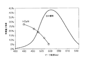
図10は、例示的な実施形態による半導体ダイのピーク波長に対する外部量子効率および目の感度の例示的な変動を示すグラフである。この例示的な実施形態では、半導体ダイは、InGaN活性層を含む。 FIG. 10 is a graph illustrating exemplary variations in external quantum efficiency and eye sensitivity versus peak wavelength of a semiconductor die according to an exemplary embodiment. In this exemplary embodiment, the semiconductor die includes an InGaN active layer.
図10を参照すると、半導体ダイの外部量子効率が低下するにつれて、ピーク波長が増大する。しかしながら、目の感度は、例えば、約520nmから約580nmまでの間の波長で、比較的高い。そして、目の感度は、照明光にとって比較的重要である場合がある。このように、LED照明光として、比較的高い目の感度を有する波長帯の光を発光することもまた、比較的重要である場合がある。したがって、比較的長い波長、例えば、約500nm以上の波長を有する光の外部量子効率を上昇させることが必要である場合がある。InGaN活性層のインジウム(In)モル比率が、光の波長を増大させるために、上昇させられる場合がある。しかしながら、そのようなInモル比率の上昇は、圧電場の増大、InGaN活性層の間の格子不整合、および/または窒化物半導体層の悪化という結果になる場合がある。さらには、Inモル比率の上昇は、Inの局所化による相分離、および、比較的低い温度での成長による不純物含有量の増加という結果になる場合がある。したがって、比較的長い波長の光効率が悪化する場合がある。 Referring to FIG. 10, the peak wavelength increases as the external quantum efficiency of the semiconductor die decreases. However, eye sensitivity is relatively high, for example, at wavelengths between about 520 nm and about 580 nm. And eye sensitivity may be relatively important for illumination light. Thus, it may be relatively important to emit light in a wavelength band having relatively high eye sensitivity as LED illumination light. Therefore, it may be necessary to increase the external quantum efficiency of light having a relatively long wavelength, for example, a wavelength of about 500 nm or more. The indium (In) molar ratio of the InGaN active layer may be increased to increase the wavelength of light. However, such an increase in In molar ratio may result in increased piezoelectric field, lattice mismatch between InGaN active layers, and / or deterioration of nitride semiconductor layers. Furthermore, an increase in In mole ratio may result in phase separation due to In localization and an increase in impurity content due to growth at relatively low temperatures. Therefore, the light efficiency of a relatively long wavelength may deteriorate.
しかしながら、少なくとも一部の例示的な実施形態によれば、半導体ダイは、ナノサイズであり、複数の半極性面を有するナノサイズの発光部を含み、それにより、比較的長い波長の光効率を上昇させる。活性層は、半極性面上に成長させられ、それが、自発分極を低減し、かつ/または、歪みを緩和することができ、それが、圧電分極を低減することができる。さらには、例えば、InGaN活性層が、ナノサイズの発光部の半極性面上に形成されるとき、歪みが緩和され得るとともに、InGaN活性層のIn含有量が増加されるときでも、結晶欠陥の発生が低減され得る。さらには、InGaN活性層の含有量は、一定、または実質的に一定であり、したがって、圧電場は抑圧される場合があり、それにより、比較的長い波長の発光効率を上昇させる。したがって、少なくとも一部の例示的な実施形態による半導体ダイは、比較的高い目の感度を有する光の比較的長い波長帯の発光効率を上昇させることにより、照明光に、より適する場合がある。さらには、様々な波長を有する複数の量子井戸層が、圧電場の発生を抑圧することにより、単一のp-n接合に含められ得るが、様々な波長を有する光の相対感度は、電流密度の変動によってあまり変動しないので、色温度の一致性が上昇する場合がある。このように、少なくとも一部の例示的な実施形態による半導体ダイ(およびそれらを含むLED)は、光照明に、より適する場合がある。 However, according to at least some example embodiments, the semiconductor die is nano-sized and includes a nano-sized light emitting portion having a plurality of semipolar surfaces, thereby providing relatively long wavelength light efficiency. Raise. The active layer is grown on a semipolar plane, which can reduce spontaneous polarization and / or alleviate strain, which can reduce piezoelectric polarization. Furthermore, for example, when the InGaN active layer is formed on the semipolar surface of the nano-sized light emitting portion, the strain can be relaxed, and even when the In content of the InGaN active layer is increased, the crystal defect Generation can be reduced. Furthermore, the content of the InGaN active layer is constant or substantially constant, so that the piezoelectric field may be suppressed, thereby increasing the emission efficiency of relatively long wavelengths. Accordingly, a semiconductor die according to at least some exemplary embodiments may be more suitable for illumination light by increasing the luminous efficiency of a relatively long wavelength band of light having a relatively high eye sensitivity. Furthermore, multiple quantum well layers with different wavelengths can be included in a single pn junction by suppressing the generation of piezoelectric fields, but the relative sensitivity of light with different wavelengths is Since there is not much variation due to variation, the color temperature consistency may increase. As such, semiconductor dies (and LEDs including them) according to at least some example embodiments may be more suitable for light illumination.
図11A〜図11Dは、例示的な実施形態による半導体ダイを製造する方法を説明するための図である。図11A〜図11Dに示される方法は、図1に示される半導体ダイを製造することに関して説明されることになる。 11A to 11D are diagrams for explaining a method of manufacturing a semiconductor die according to an exemplary embodiment. The method shown in FIGS. 11A-11D will be described with respect to manufacturing the semiconductor die shown in FIG.
図11Aを参照すると、第1の窒化物半導体層613が、基板610上に積み重ねられ、誘電層パターン615が、第1の窒化物半導体層613上に積み重ねられる。誘電パターン615は、露出部616を含み、それを通して、第1の窒化物半導体層613の部分が露出される。誘電パターン615は、誘電層をパターニングすることにより形成される。
Referring to FIG. 11A, a first
図11Bを参照すると、ベース部620が、窒化物半導体を利用して各露出部616上に成長させられる。この例では、ベース部620は、基板610に対して傾斜している半極性面を含むように成長させられる。窒化物半導体は、選択的に成長させられ、それにより、窒化物半導体は、誘電層パターン615上には成長させられない。むしろ、図示のように、窒化物半導体は、露出部616上に選択的に成長させられる。
Referring to FIG. 11B, a
図11Cおよび図11Dを参照すると、活性層625および第2の窒化物半導体層630が、ベース部620上に成長させられる。ベース部620、活性層625、および第2の窒化物半導体層630は、ナノサイズの発光部618を形成する。ナノサイズの発光部618は、ナノサイズの発光アレイ614を形成するために、所与の、所望の、または所定のギャップで配置される。
Referring to FIGS. 11C and 11D, an
図11Dに示されるように、ナノサイズの発光部618は、第1の光L1を発光することができる。ナノサイズの発光部618は、図11Dでは、所与の、所望の、または所定のギャップで配置されるが、ナノサイズの発光部618は、それらの間にギャップなしに配置される場合がある。さらには、ナノサイズの発光部618の間のギャップは、発光される光の波長を調整するために、誘電層パターン615のパターンを調整することにより調整され得る。多数の異なる波長の光が、ナノサイズの発光部618の間の2つ以上のタイプのギャップを調整することにより発光され得る。
As shown in FIG. 11D, the nano-sized
図12A〜図12Dは、別の例示的な実施形態による半導体ダイを製造する方法を説明するための図である。図12A〜図12Dに示される方法は、図5に示される半導体ダイを製造することに関して説明されることになる。 12A-12D are diagrams for explaining a method of manufacturing a semiconductor die according to another exemplary embodiment. The method shown in FIGS. 12A-12D will be described with respect to manufacturing the semiconductor die shown in FIG.
図12Aを参照すると、第1の窒化物半導体層713が、基板710上に積み重ねられ、誘電層パターン715が、第1の窒化物半導体層713上に積み重ねられる。誘電層パターン715は、露出部716を含み、それを通して、第1の窒化物半導体層713の部分が露出される。
Referring to FIG. 12A, a first
図12Bを参照すると、ベース部720が、露出部716上に成長させられる。ベース部720は、図11A〜図11Dに関して上で考察されたベース部620と同じ、または実質的に同じ方法で成長させられる。
Referring to FIG. 12B, a
図12Cを参照すると、誘電層パターン715が、第1の窒化物半導体層713の部分を露出させるために、第1の窒化物半導体層713から除去される。誘電層パターン715は、任意の既知の方法で(例えば、エッチングにより)除去され得る。
Referring to FIG. 12C, the
図12Dを参照すると、第1の活性層725が、ベース部720上に成長させられ、第2の活性層725'が、第1の窒化物半導体層713の露出された部分上に成長させられる。第1の活性層725および第2の活性層725'は、同時に、または並行的に成長させられ得る。第2の窒化物半導体層730が、第1の活性層725上に成長させられ、第3の窒化物半導体層730'が、第2の活性層725'上に成長させられる。第2の窒化物半導体層730および第3の窒化物半導体層730'は、同時に、または並行的に成長させられ得る。ベース部720、第1の活性層725、および第2の窒化物半導体層730は、ナノサイズの発光部718を形成し、一方では、第2の活性層725'および第3の窒化物半導体層730'は、多層構造742を形成する。ナノサイズの発光部718は、基板710に対して傾斜している半極性面を含む。多層構造742は、基板710と平行、または実質的に平行である非極性面を含む。
Referring to FIG. 12D, a first
ナノサイズの発光部718は、第1の波長を有する第1の光L12を発光することができ、一方では、多層構造742は、第2の波長を有する第2の光L22を発光することができる。第1の波長は、第2の波長より大きい場合がある。
Emitting
例示的な実施形態による多数の波長の光を生成する方法が、次により詳細に説明されることになる。 A method for generating multiple wavelengths of light according to an exemplary embodiment will be described in more detail below.
図19は、例示的な実施形態による単一の半導体ダイを使用して、多数の波長の光を生成するための方法を示すフローチャートである。 FIG. 19 is a flowchart illustrating a method for generating multiple wavelengths of light using a single semiconductor die according to an exemplary embodiment.
図19を参照すると、この方法は、第1の窒化物半導体層上に発光部を配置するステップ(S1702)と、発光部の間のギャップを調整するステップ(S1704)とを含む。発光部は、ナノサイズである場合があり、本明細書では、そのように説明されることになる。ナノサイズの発光部は、半極性面を含む場合がある。ナノサイズの発光部の間のギャップが調整されるとき、誘電パターンが、ナノサイズの発光部の間に配設される場合があり、または、多層構造が、それらの間に配設される場合がある。このように、多数の波長の光は、単一のチップすなわちダイで、蛍光材料の使用なしに発光され得る。ある例では、白色光は、多数の波長の光を発光することにより発光される場合があり、比較的長い波長の発光効率が、上昇する場合があり、それにより、目の感度に適した照明光を生成する。 Referring to FIG. 19, the method includes a step of arranging a light emitting part on the first nitride semiconductor layer (S1702) and a step of adjusting a gap between the light emitting parts (S1704). The light emitting portion may be nano-sized and will be described as such herein. The nano-sized light emitting part may include a semipolar surface. When the gap between the nano-sized light emitting parts is adjusted, the dielectric pattern may be disposed between the nano-sized light emitting parts, or the multilayer structure is disposed between them There is. In this way, multiple wavelengths of light can be emitted on a single chip or die without the use of fluorescent materials. In one example, white light may be emitted by emitting light of multiple wavelengths, which may increase the luminous efficiency of relatively long wavelengths, thereby illuminating suitable for eye sensitivity. Produce light.
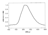
図13は、図1に示される例示的な実施形態によって構成される半導体ダイにより生成される光に関する、正規化された光ルミネセンス(PL)強度と波長との関係のグラフである。 FIG. 13 is a graph of normalized photoluminescence (PL) intensity versus wavelength for light generated by a semiconductor die configured according to the exemplary embodiment shown in FIG.
例えば、図13に示されるように、正規化されたPL強度は、約450nmから約650nmの波長の間で、大幅に変動する。そして、ピークの正規化されたPL強度は、約500nmから約550nmの間である。 For example, as shown in FIG. 13, the normalized PL intensity varies significantly between wavelengths of about 450 nm to about 650 nm. And the normalized PL intensity of the peak is between about 500 nm and about 550 nm.
図14は、図5に示される例示的な実施形態によって構成される半導体ダイにより生成される光に関する、正規化された光ルミネセンス(PL)強度と波長との関係のグラフである。 FIG. 14 is a graph of normalized photoluminescence (PL) intensity versus wavelength for light generated by a semiconductor die configured according to the exemplary embodiment shown in FIG.
図14に示されるように、半導体ダイの微小ファセット(例えば、図5の発光部118)部により生成されるピークPL強度の光に対応する波長は、半導体ダイの微小平坦部(例えば、多層構造142a)により生成される光のピークPL強度に対応する波長とは、約15nmだけ異なる。この例では、半導体ダイの微小ファセット部に関する、PL強度と波長との関係のグラフが、半導体ダイの微小平坦部に関する、PL強度と波長との関係のグラフに対して、左にシフトされている。 As shown in FIG. 14, the wavelength corresponding to the light of the peak PL intensity generated by the micro facet (for example, the light emitting unit 118 in FIG. 5) of the semiconductor die is a micro flat portion (for example, a multilayer structure) of the semiconductor die. The wavelength corresponding to the peak PL intensity of the light generated by 142a) differs by about 15 nm. In this example, the graph of the relationship between the PL intensity and the wavelength for the micro facet portion of the semiconductor die is shifted to the left with respect to the graph of the relationship between the PL intensity and the wavelength for the micro flat portion of the semiconductor die. .
図15Aおよび図15Bは、例示的な実施形態による白色光を生成するために使用可能な様々な色配置の例である。本明細書で考察されたナノサイズの発光部を、図15Aおよび図15Bに示されるパターンに従って配置することにより、白色光が、単一のチップすなわちダイで生成され得る。 15A and 15B are examples of various color arrangements that can be used to generate white light according to an exemplary embodiment. By arranging the nano-sized light emitters discussed herein according to the pattern shown in FIGS. 15A and 15B, white light can be generated on a single chip or die.
図15Aを参照すると、青色光を発光するように構成される発光部Bは、黄色光を発光するように構成される発光部Yと交互に、水平および垂直の両方向に配置される。 Referring to FIG. 15A, the light emitting unit B configured to emit blue light is alternately arranged in both the horizontal and vertical directions with the light emitting unit Y configured to emit yellow light.
図15Bを参照すると、発光部Y、青色光を発光するように構成される発光部B、および赤色光を発光するように構成される発光部Rは、交替で、水平および垂直の両方向に配置される。 Referring to FIG. 15B, the light emitting unit Y, the light emitting unit B configured to emit blue light, and the light emitting unit R configured to emit red light are alternately arranged in both horizontal and vertical directions. Is done.
図15Aおよび図15Bに示されるパターンは、単なる例である。しかしながら、例示的な実施形態は、単なるこれらの例に限定されるべきではない。むしろ、ナノサイズの発光部は、当業者により望まれるような任意の適した方法で配置され得る。 The patterns shown in FIGS. 15A and 15B are merely examples. However, the exemplary embodiments should not be limited to merely these examples. Rather, the nano-sized light emitters can be arranged in any suitable manner as desired by those skilled in the art.
図16は、例示的な実施形態による発光デバイス(LED)を示す。 FIG. 16 shows a light emitting device (LED) according to an exemplary embodiment.
図16を参照すると、半導体ダイ1612が、シリコンサブマウント1610上に配置される。シリコンサブマウント1610は、サーマルヒートシンク1608上に配置され、それは、外部パッケージ1604内に囲まれる。ボンドワイヤ1606は、シリコンサブマウント1610をLEDのアノードリード(図示せず)に接続する。カソードリード1602は、内部回路(図示せず)を介して、シリコンサブマウント1610に結合される。レンズ1614は、半導体ダイ1612、シリコンサブマウント1610およびボンドワイヤ1606を囲む。半導体ダイ1612は、本明細書で考察される半導体ダイの1つであってよい。
Referring to FIG. 16, a
例示的な実施形態による、半導体ダイおよび/またはLEDは、様々な技術分野で実施され得る。例えば、少なくとも一部の例示的な実施形態による、LEDおよび/または半導体ダイは、道路照明、装飾照明、屋内照明、生物医学用照明、車両ライトとして、フラットパネル表示装置(例えば、液晶表示(LED)装置等)での表示および/またはバックライト、ディスプレイおよび/またはプロジェクタ照明等として実施され得る。 Semiconductor dies and / or LEDs according to exemplary embodiments may be implemented in various technical fields. For example, LEDs and / or semiconductor dies, according to at least some exemplary embodiments, can be used as flat panel displays (e.g., liquid crystal displays (LEDs) as road lighting, decorative lighting, indoor lighting, biomedical lighting, vehicle lights. ) Device etc.) and / or as backlight, display and / or projector lighting etc.
本明細書で説明される例示的な実施形態は、説明された趣旨のみで解釈されるべきであり、限定を目的としたものではないということを理解されたい。それぞれの例示的な実施形態内の特徴または態様の説明は、典型的には、他の実施形態での他の同様の特徴または態様に対して利用可能であると解釈されるべきである。 It should be understood that the exemplary embodiments described herein are to be construed in the spirit of the description only and are not intended to be limiting. Descriptions of features or aspects within each exemplary embodiment are typically to be construed as available for other similar features or aspects in other embodiments.
10 基板
13 第1の窒化物半導体層
14 発光アレイ、ナノサイズの発光アレイ
14' 発光アレイ、ナノサイズの発光アレイ
15 誘電パターン部
15' 誘電パターン部
18 発光部(または構造)、発光部、ナノサイズの発光部
18a 半極性面
20 ベース部
20a 半極性面
20b 底面
25 第1の活性層
30 第2の窒化物半導体層
110 基板
113 第1の窒化物半導体層
114 発光アレイ、ナノサイズの発光アレイ
118 発光部(または構造)、発光部、ナノサイズの発光部
118a 半極性面
120 ベース部
125 第1の活性層
125' 第2の活性層
130 第2の窒化物半導体層、第2の活性層
130' 第3の窒化物半導体層
142 多層構造
142a 非極性面、多層構造
210 基板
213 第1の窒化物半導体層
214 発光アレイ、ナノサイズの発光アレイ
218 発光部(または構造)、発光部、ナノサイズの発光部
218a 半極性面
220 ベース部
225 第1の活性層
225' 第2の活性層
230 第2の窒化物半導体層
230' 第3の窒化物半導体層
240 第1の領域
242 多層構造
242a 非極性面、平坦面
250 第2の領域
310 基板
313 第1の窒化物半導体層
314 発光アレイ、ナノサイズの発光アレイ
315 誘電パターン部
318 発光部(または構造)、発光部、ナノサイズの発光部
318a 半極性面
320 ベース部
325 第1の活性層
325' 第2の活性層
330 第2の窒化物半導体層
330' 第3の窒化物半導体層
340 第1の領域
342 多層構造
342a 非極性面、平坦面
350 第2の領域
410 基板
413 第1の窒化物半導体層
414 発光アレイ、ナノサイズの発光アレイ
415 誘電パターン部
415a 第1の誘電パターン部
415b 第2の誘電パターン部
418 発光部(または構造)、発光部、ナノサイズの発光部
418a 半極性面
420 ベース部
425 第1の活性層
430 第2の窒化物半導体層
440 第1の領域
442 第2の領域
510 基板
513 第1の窒化物半導体層
514 発光アレイ、ナノサイズの発光アレイ
515 誘電パターン部
518 発光部(または構造)、発光部、ナノサイズの発光部
518a 半極性面
520 ベース部
525 第1の活性層
530 第2の窒化物半導体層
540 第1の領域
542 第2の領域
544 第3の領域
610 基板
613 第1の窒化物半導体層
614 ナノサイズの発光アレイ
615 誘電層パターン、誘電パターン
616 露出部
618 ナノサイズの発光部
620 ベース部
625 活性層
630 第2の窒化物半導体層
710 基板
713 第1の窒化物半導体層
715 誘電層パターン
716 露出部
718 ナノサイズの発光部
720 ベース部
725 第1の活性層
725' 第2の活性層
730 第2の窒化物半導体層
730' 第3の窒化物半導体層
742 多層構造
1602 カソードリード
1604 外部パッケージ
1606 ボンドワイヤ
1608 サーマルヒートシンク
1610 シリコンサブマウント
1612 半導体ダイ
1614 レンズ
1710 基板
1713 第1の窒化物半導体層
1714 発光アレイ、ナノサイズの発光アレイ
1715' 誘電パターン部
1718、1718' 発光部(または構造)、発光部、ナノサイズの発光部
1718a、1718a' 半極性面
1720、1720' ベース部
1725、1725' 第1の活性層
1730、1730' 第2の窒化物半導体層
1740 第1の領域
1742 第2の領域
1810 基板
1813 第1の窒化物半導体層
1814 発光アレイ、ナノサイズの発光アレイ
1815 誘電パターン部
1818 発光部(または構造)、発光部、ナノサイズの発光部
1818' 発光部(または構造)、発光部、ナノサイズの発光部、ナノ発光部
1818a、1818a' 半極性面
1820、1820' ベース部
1825、1825' 第1の活性層
1830、1830' 第2の窒化物半導体層
1840 第1の領域
1842 第2の領域
10 Board
13 First nitride semiconductor layer
14 Light emitting array, nano-sized light emitting array
14 'light emitting array, nano-sized light emitting array
15 Dielectric pattern
15 'Dielectric pattern
18 Light emitting part (or structure), light emitting part, nano-sized light emitting part
18a Semipolar surface
20 Base part
20a Semipolar surface
20b Bottom
25 First active layer
30 Second nitride semiconductor layer
110 substrates
113 First nitride semiconductor layer
114 light emitting array, nano-sized light emitting array
118 Light emitting part (or structure), light emitting part, nano-sized light emitting part
118a Semipolar surface
120 Base part
125 First active layer
125 'second active layer
130 Second nitride semiconductor layer, second active layer
130 'third nitride semiconductor layer
142 Multilayer structure
142a Nonpolar surface, multilayer structure
210 Board
213 First nitride semiconductor layer
214 light-emitting array, nano-sized light-emitting array
218 Light-emitting part (or structure), light-emitting part, nano-sized light-emitting part
218a Semipolar surface
220 Base part
225 First active layer
225 'second active layer
230 Second nitride semiconductor layer
230 'Third nitride semiconductor layer
240 1st area
242 Multi-layer structure
242a Nonpolar surface, flat surface
250 Second area
310 substrate
313 First nitride semiconductor layer
314 Light Emitting Array, Nano-sized Light Emitting Array
315 Dielectric pattern
318 Light emitting part (or structure), light emitting part, nano-sized light emitting part
318a Semipolar surface
320 Base part
325 1st active layer
325 'second active layer
330 Second nitride semiconductor layer
330 'Third nitride semiconductor layer
340 1st area
342 Multi-layer structure
342a Nonpolar surface, flat surface
350 Second area
410 substrates
413 First nitride semiconductor layer
414 Light-emitting array, nano-sized light-emitting array
415 Dielectric pattern
415a First dielectric pattern section
415b Second dielectric pattern
418 Light-emitting part (or structure), light-emitting part, nano-sized light-emitting part
418a Semipolar surface
420 Base part
425 1st active layer
430 Second nitride semiconductor layer
440 1st area
442 2nd area
510 board
513 First nitride semiconductor layer
514 light emitting array, nano-sized light emitting array
515 Dielectric pattern
518 Light emitting part (or structure), light emitting part, nano-sized light emitting part
518a Semipolar surface
520 Base part
525 1st active layer
530 Second nitride semiconductor layer
540 First area
542 Second area
544 3rd area
610 substrate
613 First nitride semiconductor layer
614 Nano-sized light emitting array
615 Dielectric layer pattern, dielectric pattern
616 Exposed area
618 Nano-sized light emitting part
620 Base part
625 active layer
630 Second nitride semiconductor layer
710 substrate
713 First nitride semiconductor layer
715 Dielectric layer pattern
716 Exposed part
718 Nano-sized light emitting part
720 base
725 1st active layer
725 'second active layer
730 Second nitride semiconductor layer
730 'third nitride semiconductor layer
742 Multi-layer structure
1602 Cathode lead
1604 External package
1606 Bond wire
1608 thermal heat sink
1610 silicon submount
1612 Semiconductor die
1614 lens
1710 board
1713 First nitride semiconductor layer
1714 Light-emitting array, nano-sized light-emitting array
1715 'Dielectric pattern
1718, 1718 'Light-emitting part (or structure), light-emitting part, nano-sized light-emitting part
1718a, 1718a 'semipolar surface
1720, 1720 'base
1725, 1725 'first active layer
1730, 1730 'Second nitride semiconductor layer
1740 First area
1742 2nd area
1810 substrate
1813 First nitride semiconductor layer
1814 light-emitting array, nano-sized light-emitting array
1815 Dielectric pattern
1818 Light emitting part (or structure), light emitting part, nano-sized light emitting part
1818 'light emitting part (or structure), light emitting part, nano-sized light emitting part, nano light emitting part
1818a, 1818a 'semipolar surface
1820, 1820 'base
1825, 1825 'first active layer
1830, 1830 'second nitride semiconductor layer
1840 First area
1842 Second area
Claims (42)
平坦面および複数の第2の発光構造のうちの1つを有する、少なくとも1つの第2の領域であって、前記平坦面は、前記複数の第1の発光構造の突出方向に垂直であり、前記複数の第2の発光構造は、相互に隣接して配置され、前記少なくとも1つの第2の領域は、少なくとも第2の波長を有する光を発光するように構成され、前記第2の波長は、前記第1の波長とは異なる、少なくとも1つの第2の領域と
を備える、半導体ダイ。 At least one first region configured to emit light having at least a first wavelength, comprising a plurality of first light emitting structures, wherein the plurality of first light emitting structures are the plurality At least one first region disposed with a first gap between the bases of adjacent ones of the first light emitting structures; and
At least one second region having one of a flat surface and a plurality of second light emitting structures, wherein the flat surface is perpendicular to the protruding direction of the plurality of first light emitting structures; The plurality of second light emitting structures are arranged adjacent to each other, and the at least one second region is configured to emit light having at least a second wavelength, and the second wavelength is A semiconductor die comprising: at least one second region different from the first wavelength.
をさらに備える、請求項1から3のいずれか一項に記載の半導体ダイ。 4. The dielectric layer part according to claim 1, further comprising a plurality of dielectric layer parts, each of the plurality of dielectric layer parts being disposed in a corresponding first gap. A semiconductor die according to 1.
前記複数の第1の発光構造のそれぞれは、
前記第1の窒化物半導体層と同じ材料で形成されるベース部と、
前記ベース部上に形成される第1の活性層と、
前記第1の活性層上に形成される第2の窒化物半導体層と
を含む、請求項1から6のいずれか一項に記載の半導体ダイ。 Further comprising a first nitride semiconductor layer on which the at least one first region and the at least one second region are formed;
Each of the plurality of first light emitting structures is
A base portion formed of the same material as the first nitride semiconductor layer;
A first active layer formed on the base portion;
7. The semiconductor die according to claim 1, further comprising a second nitride semiconductor layer formed on the first active layer.
第2の活性層と、
前記第2の活性層上に形成される第3の窒化物半導体層と、
平坦面と
を含む、請求項7に記載の半導体ダイ。 A plurality of multilayer structures are disposed between the plurality of first light emitting structures, and each of the plurality of multilayer structures is
A second active layer;
A third nitride semiconductor layer formed on the second active layer;
8. The semiconductor die according to claim 7, comprising a flat surface.
をさらに備える、請求項1から9のいずれか一項に記載の半導体ダイ。 10. The semiconductor die according to claim 1, further comprising a plurality of first regions and a plurality of second regions that are alternately disposed on the substrate.
前記サーマルヒートシンク上に配置されるシリコンサブマウントであって、前記少なくとも1つの半導体ダイが上に配置されるシリコンサブマウントと、
前記シリコンサブマウントに結合されるアノードリードおよびカソードリードと、
前記サーマルヒートシンクを囲む外部パッケージと、
前記シリコンサブマウントおよび前記少なくとも1つの半導体ダイを囲むレンズと
をさらに備える、請求項16に記載の発光デバイス。 A thermal heat sink,
A silicon submount disposed on the thermal heat sink, the silicon submount having the at least one semiconductor die disposed thereon;
An anode lead and a cathode lead coupled to the silicon submount;
An external package surrounding the thermal heat sink;
17. The light emitting device of claim 16, further comprising a lens surrounding the silicon submount and the at least one semiconductor die.
第2の波長を有する光を発光するように構成される複数の第2の発光構造を含む、少なくとも1つの第2の領域であって、前記複数の第2の発光構造は、前記複数の第2の発光構造のうちの隣接するもののベースの間に第2のギャップを伴って配置され、前記第2のギャップの幅は、前記第1のギャップの幅とは異なり、前記第1の波長は、前記第2の波長とは異なる、少なくとも1つの第2の領域と
を備える、半導体ダイ。 At least one first region comprising a plurality of first light emitting structures configured to emit light having a first wavelength, wherein the plurality of first light emitting structures are the plurality of first light emitting structures. At least one first region disposed with a first gap between the bases of adjacent ones of the light emitting structures;
At least one second region including a plurality of second light emitting structures configured to emit light having a second wavelength, wherein the plurality of second light emitting structures are the plurality of second light emitting structures. Between the bases of adjacent ones of the two light emitting structures with a second gap, the width of the second gap is different from the width of the first gap, and the first wavelength is A semiconductor die comprising at least one second region different from the second wavelength.
をさらに備える、請求項18に記載の半導体ダイ。 19. The semiconductor die of claim 18, further comprising a dielectric layer disposed in each of the first and second gaps.
をさらに備える、請求項18に記載の半導体ダイ。 At least one third region including a plurality of third light emitting structures configured to emit light having a third wavelength, wherein the plurality of third light emitting structures are the plurality of third light emitting structures. Between the bases of adjacent ones of the light emitting structures with a third gap, the width of the third gap being different from the width of the first and second gaps, 19. The semiconductor die of claim 18, further comprising at least one third region, wherein the third wavelength is different from the first and second wavelengths.
をさらに備える、請求項20に記載の半導体ダイ。 21. The semiconductor die of claim 20, further comprising a dielectric layer disposed in each of the first, second and third gaps.
前記複数の第1の発光構造および前記複数の第2の発光構造のそれぞれは、
前記第1の窒化物半導体層と同じ材料で形成されるベース部と、
前記ベース部上に形成される第1の活性層と、
前記第1の活性層上に形成される第2の窒化物半導体層と
を含む、請求項18から24のいずれか一項に記載の半導体ダイ。 Further comprising a first nitride semiconductor layer on which the at least one first region and the at least one second region are formed;
Each of the plurality of first light emitting structures and the plurality of second light emitting structures is:
A base portion formed of the same material as the first nitride semiconductor layer;
A first active layer formed on the base portion;
25. The semiconductor die according to any one of claims 18 to 24, further comprising a second nitride semiconductor layer formed on the first active layer.
を備える発光デバイス。 26. A light emitting device comprising at least one semiconductor die according to any one of claims 18 to 25.
前記サーマルヒートシンク上に配置されるシリコンサブマウントであって、前記少なくとも1つの半導体ダイが上に配置されるシリコンサブマウントと、
前記シリコンサブマウントに結合されるアノードリードおよびカソードリードと、
前記サーマルヒートシンクを囲む外部パッケージと、
前記シリコンサブマウントおよび前記少なくとも1つの半導体ダイを囲むレンズと
をさらに備える、請求項26に記載の発光デバイス。 A thermal heat sink,
A silicon submount disposed on the thermal heat sink, the silicon submount having the at least one semiconductor die disposed thereon;
An anode lead and a cathode lead coupled to the silicon submount;
An external package surrounding the thermal heat sink;
27. The light emitting device of claim 26, further comprising a lens surrounding the silicon submount and the at least one semiconductor die.
前記第1のサイズとは異なる第2のサイズを有する複数の第2の発光構造を含む、少なくとも1つの第2の領域であって、前記複数の第2の発光構造は、前記複数の第2の発光構造のうちの隣接するもののベースの間に第2のギャップを伴って配置され、第2の波長を有する光を発光するように構成される、少なくとも1つの第2の領域と
を備え、前記第1の波長および前記第2の波長は、異なるものであり、前記第1および第2のギャップの幅は、同じである、半導体ダイ。 At least one first region including a plurality of first light emitting structures having a first size, wherein the plurality of first light emitting structures are adjacent to each other among the plurality of first light emitting structures. At least one first region disposed with a first gap between the bases of the ones and configured to emit light having a first wavelength;
At least one second region including a plurality of second light emitting structures having a second size different from the first size, wherein the plurality of second light emitting structures are the plurality of second light emitting structures. At least one second region disposed with a second gap between the bases of adjacent ones of the light emitting structures and configured to emit light having a second wavelength; The semiconductor die, wherein the first wavelength and the second wavelength are different, and the widths of the first and second gaps are the same.
前記複数の第1の発光構造のそれぞれ、および前記複数の第2の発光構造のそれぞれは、
前記第1の窒化物半導体層と同じ材料で形成されるベース部と、
前記ベース部上に形成される第1の活性層と、
前記第1の活性層上に形成される第2の窒化物半導体層と
を含む、請求項28に記載の半導体ダイ。 Further comprising a first nitride semiconductor layer on which the at least one first region and the at least one second region are formed;
Each of the plurality of first light emitting structures and each of the plurality of second light emitting structures are:
A base portion formed of the same material as the first nitride semiconductor layer;
A first active layer formed on the base portion;
30. The semiconductor die of claim 28, comprising a second nitride semiconductor layer formed on the first active layer.
をさらに備える、請求項28に記載の半導体ダイ。 30. The semiconductor die of claim 28, further comprising a dielectric layer disposed in each of the first and second gaps.
を備える発光デバイス。 32. A light emitting device comprising at least one semiconductor die according to any one of claims 28 to 31.
前記サーマルヒートシンク上に配置されるシリコンサブマウントであって、前記少なくとも1つの半導体ダイが上に配置されるシリコンサブマウントと、
前記シリコンサブマウントに結合されるアノードリードおよびカソードリードと、
前記サーマルヒートシンクを囲む外部パッケージと、
前記シリコンサブマウントおよび前記少なくとも1つの半導体ダイを囲むレンズと
をさらに備える、請求項32に記載の発光デバイス。 A thermal heat sink,
A silicon submount disposed on the thermal heat sink, the silicon submount having the at least one semiconductor die disposed thereon;
An anode lead and a cathode lead coupled to the silicon submount;
An external package surrounding the thermal heat sink;
33. The light emitting device of claim 32, further comprising a lens surrounding the silicon submount and the at least one semiconductor die.
第2の波長を有する光を発光するように構成される、複数の平坦な発光面であって、前記複数の発光構造および前記複数の平坦な発光面は、交互に基板上に配置され、前記第1の波長は、前記第2の波長とは異なる、複数の平坦な発光面と
を備える、半導体ダイ。 A plurality of light emitting structures configured to emit light having a first wavelength;
A plurality of flat light emitting surfaces configured to emit light having a second wavelength, wherein the plurality of light emitting structures and the plurality of flat light emitting surfaces are alternately disposed on a substrate; A semiconductor die, wherein the first wavelength comprises a plurality of flat light emitting surfaces different from the second wavelength.
前記複数の発光構造のそれぞれは、
前記第1の窒化物半導体層と同じ材料で形成されるベース部と、
前記ベース部上に形成される第1の活性層と、
前記第1の活性層上に形成される第2の窒化物半導体層と
を含む、請求項34から36のいずれか一項に記載の半導体ダイ。 Further comprising a first nitride semiconductor layer on which the plurality of light emitting structures and the plurality of flat light emitting surfaces are formed;
Each of the plurality of light emitting structures is
A base portion formed of the same material as the first nitride semiconductor layer;
A first active layer formed on the base portion;
37. The semiconductor die according to claim 34, further comprising a second nitride semiconductor layer formed on the first active layer.
前記複数の平坦な発光面のそれぞれは、
第2の活性層と、
前記第2の活性層上に形成される第3の窒化物半導体層と、
非極性面と
を含む構造を有する、請求項34から37のいずれか一項に記載の半導体ダイ。 Further comprising a first nitride semiconductor layer on which the plurality of light emitting structures and the plurality of flat light emitting surfaces are formed;
Each of the plurality of flat light emitting surfaces is
A second active layer;
A third nitride semiconductor layer formed on the second active layer;
38. The semiconductor die according to any one of claims 34 to 37, having a structure including a nonpolar plane.
を備える発光デバイス。 39. A light emitting device comprising at least one semiconductor die according to any one of claims 34 to 38.
前記サーマルヒートシンク上に配置されるシリコンサブマウントであって、前記少なくとも1つの半導体ダイが上に配置されるシリコンサブマウントと、
前記シリコンサブマウントに結合されるアノードリードおよびカソードリードと、
前記サーマルヒートシンクを囲む外部パッケージと、
前記シリコンサブマウントおよび前記少なくとも1つの半導体ダイを囲むレンズと
をさらに備える、請求項39に記載の発光デバイス。 A thermal heat sink,
A silicon submount disposed on the thermal heat sink, the silicon submount having the at least one semiconductor die disposed thereon;
An anode lead and a cathode lead coupled to the silicon submount;
An external package surrounding the thermal heat sink;
40. The light emitting device of claim 39, further comprising a lens surrounding the silicon submount and the at least one semiconductor die.
基板上に第1の窒化物半導体層を形成するステップと、
前記第1の窒化物半導体層の部分を露出させるために、前記第1の窒化物半導体層上に形成される誘電層をパターニングするステップと、
前記第1の窒化物半導体層のそれぞれの露出された部分上にベース構造を形成するステップであって、前記ベース構造は前記第1の窒化物半導体層と同じ材料で形成されるステップと、
各ベース構造上に活性層を形成するステップと、
前記活性層上に第2の窒化物半導体層を形成するステップと
を含む方法。 A method of manufacturing a semiconductor die, comprising:
Forming a first nitride semiconductor layer on a substrate;
Patterning a dielectric layer formed on the first nitride semiconductor layer to expose a portion of the first nitride semiconductor layer;
Forming a base structure on each exposed portion of the first nitride semiconductor layer, wherein the base structure is formed of the same material as the first nitride semiconductor layer;
Forming an active layer on each base structure;
Forming a second nitride semiconductor layer on the active layer.
前記活性層および前記第2の窒化物半導体層は、それぞれのベース構造、および前記ベース構造の隣接するものの間の前記第1の窒化物半導体層の露出された部分の上に、順次形成される、請求項41に記載の方法。 Removing the patterned dielectric layer before forming the active layer and the second nitride semiconductor layer;
The active layer and the second nitride semiconductor layer are sequentially formed on each base structure and an exposed portion of the first nitride semiconductor layer between adjacent ones of the base structure. 42. The method of claim 41.
Applications Claiming Priority (2)
| Application Number | Priority Date | Filing Date | Title |
|---|---|---|---|
| KR10-2010-0051432 | 2010-05-31 | ||
| KR1020100051432A KR20110131801A (en) | 2010-05-31 | 2010-05-31 | How to make light emitting devices and multi-wavelength light |
Publications (1)
| Publication Number | Publication Date |
|---|---|
| JP2011254078A true JP2011254078A (en) | 2011-12-15 |
Family
ID=44117994
Family Applications (1)
| Application Number | Title | Priority Date | Filing Date |
|---|---|---|---|
| JP2011121587A Pending JP2011254078A (en) | 2010-05-31 | 2011-05-31 | Semiconductor die, light-emitting device, method of manufacturing the same, and method of generating multiple-wavelength light |
Country Status (5)
| Country | Link |
|---|---|
| US (1) | US8399876B2 (en) |
| EP (1) | EP2390930A3 (en) |
| JP (1) | JP2011254078A (en) |
| KR (1) | KR20110131801A (en) |
| CN (1) | CN102263172B (en) |
Cited By (3)
| Publication number | Priority date | Publication date | Assignee | Title |
|---|---|---|---|---|
| US9287445B2 (en) | 2012-12-14 | 2016-03-15 | Samsung Electronics Co., Ltd. | Nano-structured light-emitting devices |
| JP2023519468A (en) * | 2020-03-27 | 2023-05-11 | グーグル エルエルシー | Indium gallium nitride light-emitting diode with reduced strain |
| JP2023541295A (en) * | 2020-09-15 | 2023-09-29 | アプライド マテリアルズ インコーポレイテッド | Tricolor light source integrated on a single wafer |
Families Citing this family (31)
| Publication number | Priority date | Publication date | Assignee | Title |
|---|---|---|---|---|
| KR20110131801A (en) * | 2010-05-31 | 2011-12-07 | 삼성전자주식회사 | How to make light emitting devices and multi-wavelength light |
| KR101660407B1 (en) | 2010-11-19 | 2016-09-27 | 삼성전자주식회사 | Active optical device employing phase change material |
| KR101964890B1 (en) | 2011-07-12 | 2019-04-03 | 삼성전자주식회사 | Nano-structured light emitting device |
| KR20130106690A (en) * | 2012-03-20 | 2013-09-30 | 삼성전자주식회사 | White light emitting diode |
| CN104396028B (en) * | 2012-05-24 | 2018-01-19 | 香港大学 | White nano light-emitting diode without color conversion |
| CN102832306B (en) * | 2012-08-29 | 2015-09-30 | 扬州中科半导体照明有限公司 | A kind of epitaxial structure of high brightness LED and its implementation |
| US9000414B2 (en) * | 2012-11-16 | 2015-04-07 | Korea Photonics Technology Institute | Light emitting diode having heterogeneous protrusion structures |
| KR102018615B1 (en) * | 2013-01-18 | 2019-09-05 | 삼성전자주식회사 | Semiconductor light emitting device and manufacturing method of the same |
| KR101977677B1 (en) * | 2013-02-05 | 2019-05-13 | 삼성전자주식회사 | Semiconductor light emitting device |
| US9054233B2 (en) * | 2013-06-07 | 2015-06-09 | Glo Ab | Multicolor LED and method of fabricating thereof |
| KR101471608B1 (en) * | 2013-06-12 | 2014-12-11 | 광주과학기술원 | Nitride based light emitting diode including nanorods and method for manufacturing the same |
| US9412911B2 (en) | 2013-07-09 | 2016-08-09 | The Silanna Group Pty Ltd | Optical tuning of light emitting semiconductor junctions |
| KR102132651B1 (en) | 2013-12-03 | 2020-07-10 | 삼성전자주식회사 | Nano structure semiconductor light emitting device |
| KR20150092674A (en) | 2014-02-05 | 2015-08-13 | 삼성전자주식회사 | Light emitting device and light emitting device package |
| CN103943740B (en) * | 2014-05-13 | 2016-09-07 | 湘能华磊光电股份有限公司 | Increase LED outer layer growth method and the LED epitaxial layer of luminous efficiency |
| CN104465929B (en) * | 2014-11-07 | 2017-09-12 | 中山大学 | The III-nitride micro-nano luminescent device and preparation method of embedded active layer |
| KR101653530B1 (en) * | 2014-12-30 | 2016-09-02 | (재)한국나노기술원 | manufacturing method of white LED using nano-structure and white LED thereby |
| FR3032064B1 (en) | 2015-01-22 | 2018-03-09 | Aledia | OPTOELECTRONIC DEVICE AND METHOD FOR MANUFACTURING THE SAME |
| JP6156402B2 (en) * | 2015-02-13 | 2017-07-05 | 日亜化学工業株式会社 | Light emitting device |
| CN104810448A (en) * | 2015-03-27 | 2015-07-29 | 中山大学 | Transverse conducting GaN-based luminescent device growing and preparing method |
| KR101666836B1 (en) * | 2015-08-20 | 2016-10-17 | 한국산업기술대학교산학협력단 | Growth technique for phosphor-free white light emitting diode |
| FR3041068B1 (en) * | 2015-09-15 | 2017-09-15 | Valeo Vision | LIGHTING AND / OR SIGNALING DEVICE FOR MOTOR VEHICLE |
| KR101721846B1 (en) * | 2015-12-30 | 2017-04-03 | (재)한국나노기술원 | manufacturing method of micro GaN LED array and micro GaN LED array thereby |
| DE102016104616B4 (en) * | 2016-03-14 | 2021-09-23 | OSRAM Opto Semiconductors Gesellschaft mit beschränkter Haftung | Semiconductor light source |
| CN105957927B (en) * | 2016-05-31 | 2018-04-24 | 华灿光电(苏州)有限公司 | A kind of growing method of LED epitaxial slice |
| FR3054292B1 (en) | 2016-07-22 | 2019-04-05 | Valeo Vision | LIGHT MODULE OF LAND VEHICLE |
| WO2018057041A1 (en) * | 2016-09-26 | 2018-03-29 | Intel Corporation | Monolithic multi-color light emitting pixel |
| KR102506441B1 (en) * | 2017-12-04 | 2023-03-06 | 삼성전자주식회사 | Fabrication method of semiconductor light emitting array and semiconductor light emitting array |
| KR102050407B1 (en) | 2017-12-29 | 2019-12-02 | 한국광기술원 | Vertically stacked multi-wavelength light emitting device |
| FR3087942B1 (en) | 2018-10-29 | 2021-09-17 | Commissariat Energie Atomique | MULTI-COLOR ELECTROLUMINESCENT DISPLAY DEVICE AND METHOD FOR MANUFACTURING SUCH A DEVICE |
| CN110379761B (en) * | 2019-07-18 | 2021-08-24 | 京东方科技集团股份有限公司 | Micro-LED transfer substrate and device |
Citations (4)
| Publication number | Priority date | Publication date | Assignee | Title |
|---|---|---|---|---|
| JP2000031595A (en) * | 1998-07-10 | 2000-01-28 | Nec Corp | Optical semiconductor element as well as method and apparatus for manufacture of optical semiconductor element |
| JP2002100804A (en) * | 2000-07-18 | 2002-04-05 | Sony Corp | Semiconductor light emitting element and semiconductor light emitting device |
| JP2002185040A (en) * | 2000-12-15 | 2002-06-28 | Sony Corp | Semiconductor light emitting device and method of manufacturing semiconductor light emitting device |
| JP2002335016A (en) * | 2001-03-06 | 2002-11-22 | Sony Corp | Display device and semiconductor light emitting device |
Family Cites Families (19)
| Publication number | Priority date | Publication date | Assignee | Title |
|---|---|---|---|---|
| JPS61134000A (en) * | 1984-12-05 | 1986-06-21 | 株式会社日立製作所 | Speech analysis and synthesis method |
| KR100214588B1 (en) | 1996-01-29 | 1999-08-02 | 구자홍 | Light emitting device array structure and manufacturing method thereof |
| JP3882539B2 (en) * | 2000-07-18 | 2007-02-21 | ソニー株式会社 | Semiconductor light emitting device, method for manufacturing the same, and image display device |
| JP2003218395A (en) | 2002-01-18 | 2003-07-31 | Sony Corp | Semiconductor light emitting element, semiconductor laser element and light emitting device using the same |
| JP3899936B2 (en) * | 2002-01-18 | 2007-03-28 | ソニー株式会社 | Semiconductor light emitting device and manufacturing method thereof |
| JP2004119964A (en) | 2002-09-06 | 2004-04-15 | Sony Corp | Semiconductor light emitting element manufacturing method, semiconductor light emitting element, integrated semiconductor light emitting device manufacturing method, integrated semiconductor light emitting device, image display device manufacturing method, image display device, lighting device manufacturing method, and lighting device |
| US7002182B2 (en) | 2002-09-06 | 2006-02-21 | Sony Corporation | Semiconductor light emitting device integral type semiconductor light emitting unit image display unit and illuminating unit |
| JP2004206057A (en) * | 2002-11-01 | 2004-07-22 | Omron Corp | Optical multiplexer / demultiplexer and method of manufacturing optical multiplexer / demultiplexer |
| US7348600B2 (en) * | 2003-10-20 | 2008-03-25 | Nichia Corporation | Nitride semiconductor device, and its fabrication process |
| WO2006099211A2 (en) | 2005-03-11 | 2006-09-21 | Ponce Fernando A | Solid state light emitting device |
| KR100649769B1 (en) * | 2005-12-28 | 2006-11-27 | 삼성전기주식회사 | Semiconductor Light Emitting Diode and Manufacturing Method Thereof |
| JP4802316B2 (en) * | 2006-01-24 | 2011-10-26 | シャープ株式会社 | Nitride-based semiconductor light-emitting device and manufacturing method thereof |
| KR100755598B1 (en) | 2006-06-30 | 2007-09-06 | 삼성전기주식회사 | Nitride Semiconductor Light Emitting Array |
| KR100809234B1 (en) | 2006-08-21 | 2008-03-05 | 삼성전기주식회사 | Nitride semiconductor light emitting device manufacturing method |
| US20080149946A1 (en) * | 2006-12-22 | 2008-06-26 | Philips Lumileds Lighting Company, Llc | Semiconductor Light Emitting Device Configured To Emit Multiple Wavelengths Of Light |
| KR100857410B1 (en) | 2007-03-08 | 2008-09-08 | 전북대학교산학협력단 | Manufacturing method of white LED |
| TW201044568A (en) * | 2009-04-20 | 2010-12-16 | 3M Innovative Properties Co | Non-radiatively pumped wavelength converter |
| KR20110131801A (en) * | 2010-05-31 | 2011-12-07 | 삼성전자주식회사 | How to make light emitting devices and multi-wavelength light |
| KR101643757B1 (en) * | 2010-06-01 | 2016-07-29 | 삼성전자주식회사 | Light emitting device and method of manufacturing the same |
-
2010
- 2010-05-31 KR KR1020100051432A patent/KR20110131801A/en not_active Ceased
-
2011
- 2011-05-27 EP EP11167854.6A patent/EP2390930A3/en not_active Withdrawn
- 2011-05-31 US US13/149,357 patent/US8399876B2/en active Active
- 2011-05-31 JP JP2011121587A patent/JP2011254078A/en active Pending
- 2011-05-31 CN CN201110144449.1A patent/CN102263172B/en not_active Expired - Fee Related
Patent Citations (4)
| Publication number | Priority date | Publication date | Assignee | Title |
|---|---|---|---|---|
| JP2000031595A (en) * | 1998-07-10 | 2000-01-28 | Nec Corp | Optical semiconductor element as well as method and apparatus for manufacture of optical semiconductor element |
| JP2002100804A (en) * | 2000-07-18 | 2002-04-05 | Sony Corp | Semiconductor light emitting element and semiconductor light emitting device |
| JP2002185040A (en) * | 2000-12-15 | 2002-06-28 | Sony Corp | Semiconductor light emitting device and method of manufacturing semiconductor light emitting device |
| JP2002335016A (en) * | 2001-03-06 | 2002-11-22 | Sony Corp | Display device and semiconductor light emitting device |
Cited By (6)
| Publication number | Priority date | Publication date | Assignee | Title |
|---|---|---|---|---|
| US9287445B2 (en) | 2012-12-14 | 2016-03-15 | Samsung Electronics Co., Ltd. | Nano-structured light-emitting devices |
| US9525100B2 (en) | 2012-12-14 | 2016-12-20 | Samsung Electronics Co., Ltd. | Nano-structured light-emitting devices |
| JP2023519468A (en) * | 2020-03-27 | 2023-05-11 | グーグル エルエルシー | Indium gallium nitride light-emitting diode with reduced strain |
| JP7699127B2 (en) | 2020-03-27 | 2025-06-26 | グーグル エルエルシー | Reduced distortion indium gallium nitride light emitting diodes |
| JP2023541295A (en) * | 2020-09-15 | 2023-09-29 | アプライド マテリアルズ インコーポレイテッド | Tricolor light source integrated on a single wafer |
| JP7564346B2 (en) | 2020-09-15 | 2024-10-08 | アプライド マテリアルズ インコーポレイテッド | Three-color light source integrated on a single wafer. |
Also Published As
| Publication number | Publication date |
|---|---|
| CN102263172A (en) | 2011-11-30 |
| CN102263172B (en) | 2016-03-30 |
| KR20110131801A (en) | 2011-12-07 |
| EP2390930A2 (en) | 2011-11-30 |
| US8399876B2 (en) | 2013-03-19 |
| US20110291072A1 (en) | 2011-12-01 |
| EP2390930A3 (en) | 2013-09-18 |
Similar Documents
| Publication | Publication Date | Title |
|---|---|---|
| CN102263172B (en) | The method of semiconductor chip, luminescent device and manufacture semiconductor chip | |
| US8124990B2 (en) | Semiconductor light emitting device having an electron barrier layer between a plurality of active layers | |
| CN103325899A (en) | White light emitting diode | |
| US9780260B2 (en) | Semiconductor light emitting device and manufacturing method of the same | |
| KR102397663B1 (en) | Semiconductor light-emitting device | |
| CN102067338A (en) | Semiconductor light-emitting devices for producing arbitrary colors | |
| KR102397662B1 (en) | Semiconductor light-emitting element | |
| CN102347431A (en) | Semiconductor light emitting diode component | |
| KR101666836B1 (en) | Growth technique for phosphor-free white light emitting diode | |
| KR101285164B1 (en) | Semiconductor light emitting device and method for manufacturing the same | |
| CN105405946A (en) | Light emitting diode crystal grain and manufacturing method thereof | |
| KR20110102061A (en) | LED element and manufacturing method thereof | |
| KR102261727B1 (en) | Light emitting device and light emitting device package including the same | |
| KR20080030404A (en) | LED chip manufacturing method | |
| KR101504155B1 (en) | Nitride semiconductor light emitting element | |
| KR102163978B1 (en) | Light emitting device and lighting system having the same | |
| TWI816705B (en) | Semiconductor type phosphor | |
| KR100608919B1 (en) | Light emitting device and manufacturing method thereof | |
| KR20170123061A (en) | Optical device of multi-wave band and method for manufacturing thereof | |
| KR102355608B1 (en) | Light emitting apparatus | |
| KR101562928B1 (en) | Light Emitting Diode and manufacturing method of the same | |
| JP2007081182A (en) | Semiconductor light emitting device | |
| KR20170048725A (en) | Light emitting diode, and light system having the same | |
| KR20160056039A (en) | Light emitting device and lighting system | |
| WO2016152453A1 (en) | Semiconductor light-emitting element |
Legal Events
| Date | Code | Title | Description |
|---|---|---|---|
| A621 | Written request for application examination |
Free format text: JAPANESE INTERMEDIATE CODE: A621 Effective date: 20140519 |
|
| RD04 | Notification of resignation of power of attorney |
Free format text: JAPANESE INTERMEDIATE CODE: A7424 Effective date: 20141226 |
|
| A131 | Notification of reasons for refusal |
Free format text: JAPANESE INTERMEDIATE CODE: A131 Effective date: 20150126 |
|
| A521 | Request for written amendment filed |
Free format text: JAPANESE INTERMEDIATE CODE: A523 Effective date: 20150424 |
|
| A02 | Decision of refusal |
Free format text: JAPANESE INTERMEDIATE CODE: A02 Effective date: 20150608 |
|
| A521 | Request for written amendment filed |
Free format text: JAPANESE INTERMEDIATE CODE: A523 Effective date: 20151008 |
|
| A911 | Transfer to examiner for re-examination before appeal (zenchi) |
Free format text: JAPANESE INTERMEDIATE CODE: A911 Effective date: 20151015 |
|
| A912 | Re-examination (zenchi) completed and case transferred to appeal board |
Free format text: JAPANESE INTERMEDIATE CODE: A912 Effective date: 20151204 |
|
| A521 | Request for written amendment filed |
Free format text: JAPANESE INTERMEDIATE CODE: A523 Effective date: 20160906 |