JP2011170758A - Processor - Google Patents
Processor Download PDFInfo
- Publication number
- JP2011170758A JP2011170758A JP2010036027A JP2010036027A JP2011170758A JP 2011170758 A JP2011170758 A JP 2011170758A JP 2010036027 A JP2010036027 A JP 2010036027A JP 2010036027 A JP2010036027 A JP 2010036027A JP 2011170758 A JP2011170758 A JP 2011170758A
- Authority
- JP
- Japan
- Prior art keywords
- instruction
- type
- processing
- stage
- register
- Prior art date
- Legal status (The legal status is an assumption and is not a legal conclusion. Google has not performed a legal analysis and makes no representation as to the accuracy of the status listed.)
- Withdrawn
Links
Images


Landscapes
- Executing Machine-Instructions (AREA)
- Programmable Controllers (AREA)
Abstract
Description
本発明は、パイプライン処理により高速演算を実現するプロセッサに関する。 The present invention relates to a processor that realizes high-speed computation by pipeline processing.
近年、高速化の要求が高いプログラマブルロジックコントローラ(PLC)などにおいては、通信処理や周辺処理を行う汎用マイクロプロセッサと、ビット演算処理命令などの命令を処理する専用のプロセッサとを組み合わせることで高速化を実現している。 In recent years, programmable logic controllers (PLCs), which have high demands for speeding up, can be speeded up by combining a general-purpose microprocessor that performs communication processing and peripheral processing with a dedicated processor that processes instructions such as bit operation processing instructions. Is realized.
この種のプロセッサは、ビット演算処理を主とする基本命令と、複数のビットで構成されるデータを扱う応用命令などの各命令をパイプライン実行することで、高速化を実現している(例えば、特許文献1を参照)。特許文献1に記載のPLCでは、専用のハードウェア(プロセッサ)によって、5段パイプライン構造が構成されており、パイプライン処理の各実行ステージでは、次に示す処理が行われる。
第1ステージ:命令メモリから次に実行する命令を取り出す命令フェッチ処理。
第2ステージ:命令デコード処理、及び、汎用レジスタから値を取り出すレジスタフェッチ処理。
第3ステージ:算術論理演算処理、データアドレス計算処理、分岐先計算処理の何れか。
第4ステージ:データメモリへのアクセス処理。
第5ステージ:ビット演算処理、汎用レジスタへの書き込み処理、分岐処理の何れか。
This type of processor achieves high speed by executing each instruction such as a basic instruction mainly for bit operation processing and an application instruction that handles data composed of a plurality of bits (for example, , See Patent Document 1). In the PLC described in
First stage: Instruction fetch processing for fetching the next instruction to be executed from the instruction memory.
Second stage: instruction decode processing and register fetch processing for fetching a value from a general-purpose register.
Third stage: Any of arithmetic logic operation processing, data address calculation processing, and branch destination calculation processing.
Fourth stage: access processing to the data memory.
Fifth stage: Bit operation processing, general-purpose register write processing, or branch processing.
ところで、上述のようなプロセッサにおける命令の処理時間は、パイプライン処理の各実行ステージのうち最も処理時間が長い実行ステージの処理時間によって決定される。高速化を実現するためには、各実行ステージにおける処理時間をパイプライン処理の1クロック分の時間以内で、且つ、各実行ステージの処理時間が等しくなるように設定する必要がある。 By the way, the instruction processing time in the processor as described above is determined by the processing time of the execution stage having the longest processing time among the execution stages of the pipeline processing. In order to achieve high speed, it is necessary to set the processing time in each execution stage to be within the time of one clock of the pipeline processing and equal in processing time in each execution stage.
しかしながら、上述した従来のプロセッサでは、命令ごとの処理内容によらず共通のハードウェアを用いてパイプライン実行するので、命令デコード処理時には、処理が不要なハードウェアにて処理が行われないよう各種制御が行われる。そのため、プロセッサで実行可能な命令を増やすと、命令デコード処理に必要な時間が長くなり、第2ステージにおける処理時間がパイプライン処理の1クロック分の時間内に収まらない恐れがあった。これにより、例えば図3(b)に示すように、第2ステージにおいて命令デコード処理(図中のID)が終了するまで後段のパイプライン処理が停止して(図中のNOP)、処理速度が低下するという問題があった。 However, in the above-described conventional processor, pipeline execution is performed using common hardware regardless of the processing contents for each instruction, so that various processing is performed so that processing is not performed by hardware that does not require processing during instruction decoding processing. Control is performed. For this reason, when the number of instructions that can be executed by the processor is increased, the time required for the instruction decoding process becomes longer, and the processing time in the second stage may not be within the time of one clock of the pipeline processing. As a result, for example, as shown in FIG. 3B, the pipeline processing in the subsequent stage is stopped (NOP in the drawing) until the instruction decoding processing (ID in the drawing) is completed in the second stage, and the processing speed is increased. There was a problem of lowering.
本発明は、上記事由に鑑みて為されたものであり、その目的とするところは、実行可能な命令を増やした場合でも、高速に演算が可能なプロセッサを提供することにある。 The present invention has been made in view of the above reasons, and an object of the present invention is to provide a processor capable of high-speed computation even when the number of executable instructions is increased.
上記目的を達成するために、第1の発明では、命令パイプライン処理の各実行ステージを構成するハードウェアとして、実行対象の命令を格納する命令メモリと、前記命令メモリから次に実行する命令のアドレスを格納するプログラムカウンタと、命令フェッチ処理により前記命令メモリから読み出された前記命令が格納される命令レジスタと、前記命令レジスタに格納された命令に基づいて、汎用レジスタからの読み込みを行う命令デコーダと、複数の汎用レジスタからなる汎用レジスタブロックと、データメモリとそのデータメモリへのアクセス制御を行うメモリアクセスインタフェースと、算術論理演算処理を行う算術論理演算ユニットと、ビット演算処理を行うビット演算ユニットと、各実行ステージ間をつなぐ複数のパイプラインレジスタとを備え、処理内容に基づいて分類される命令タイプごとに、前記ハードウェアを組み合わせて構成される複数の命令タイプ別実行ステージを有し、前記命令デコーダは、前記命令タイプに基づいて前記実行ステージへの分岐を行うことを特徴とする。 In order to achieve the above object, according to the first aspect of the present invention, as hardware constituting each execution stage of the instruction pipeline processing, an instruction memory for storing an instruction to be executed, an instruction to be executed next from the instruction memory, A program counter for storing an address; an instruction register for storing the instruction read from the instruction memory by instruction fetch processing; and an instruction for reading from a general-purpose register based on the instruction stored in the instruction register Decoder, general-purpose register block composed of a plurality of general-purpose registers, a data memory and a memory access interface for controlling access to the data memory, an arithmetic logic unit for performing arithmetic logic operation processing, and a bit operation for performing bit operation processing Multiple pipelines connecting the unit and each execution stage Each instruction type classified based on processing content, and a plurality of instruction type-specific execution stages configured by combining the hardware, and the instruction decoder based on the instruction type It is characterized by branching to the execution stage.
第2の発明では、第1の発明において、前記命令コードは、前記命令タイプに対応した識別コードを有し、前記命令デコーダは、前記識別コードに基づいて命令タイプを判別することを特徴とする。 According to a second invention, in the first invention, the instruction code has an identification code corresponding to the instruction type, and the instruction decoder determines the instruction type based on the identification code. .
本発明によれば、命令デコードにかかる時間を短くすることで、処理可能な命令数を増やした場合でも、高速に処理が可能なプロセッサを提供することができる。 According to the present invention, it is possible to provide a processor capable of high-speed processing even when the number of instructions that can be processed is increased by shortening the time required for instruction decoding.
以下、本発明の実施の形態について、図1〜図3に基づいて説明する。本実施の形態にかかるプロセッサ1は、例えば、通信処理や周辺処理を行う汎用マイクロプロセッサとともにPLCを構成し、各種命令をパイプライン実行することで、高速化を実現したプロセッサである。
Hereinafter, embodiments of the present invention will be described with reference to FIGS. The
プロセッサ1が処理する各命令は、命令に応じて行われる処理の内容や、処理時にアクセスするメモリなどのリソースに基づいて、複数の命令タイプに分類される。本実施の形態においては、後述するプロセッサ1の命令デコーダCTRLにより、Mタイプ命令、Rタイプ命令、Jタイプ命令、Bタイプ命令の4つの命令タイプに分類している。
Each instruction processed by the
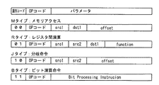
各命令の構造は、図2に示すように、識別コードフィールドと、識別コードに続くopコードフィールドと、opコードフィールドに続くパラメータフィールドとで構成されており、命令タイプに応じて識別コードフィールドの値が決定されている。また、opコードは、同一の命令タイプないでは、重複しないような値に設定されており、識別コードとopコードの両方から、一意に命令が導き出せるようになっている。 As shown in FIG. 2, the structure of each instruction includes an identification code field, an op code field following the identification code, and a parameter field following the op code field. The value has been determined. The op code is set to a value that does not overlap if the same instruction type is not used, and the instruction can be uniquely derived from both the identification code and the op code.
ここで、Mタイプ命令は、主にデータメモリ3(図1を参照)に格納された値へのアクセスを含む命令であり、識別コードは2進で00が設定されている。またMタイプ命令のパラメータフィールドは、src1フィールド、dst1フィールド、及び、offsetフィールドで構成されている。具体的には、src1フィールドで指定されるレジスタの値と、offsetフィールドの値から実効アドレスを求め、データメモリ3に格納されている値をdst1フィールドで指示された汎用レジスタに読み出すという処理を行う命令(LOAD命令)などである。
Here, the M type instruction is an instruction mainly including access to a value stored in the data memory 3 (see FIG. 1), and 00 is set as the identification code in binary. The parameter field of the M type instruction includes a src1 field, a dst1 field, and an offset field. Specifically, an effective address is obtained from the value of the register specified in the src1 field and the value of the offset field, and the value stored in the
Rタイプ命令は、主に汎用レジスタ間での演算や、汎用レジスタの値と定数との演算を行う命令であり、識別コードは2進で01が設定されている。またRタイプ命令のパラメータフィールドは、src1フィールド、src2フィールド、dst1フィールド、及び、functionフィールドとで構成されている。具体的には、src1フィールドで指定される汎用レジスタの値と、src2フィールドで指定される汎用レジスタ値との和を、dst1フィールドで指示された汎用レジスタに書き込むという処理を行う命令(ADD命令)などである。なおfunctionフィールドは、例えば、演算方法の詳細仕様の指定に用いられる。 The R type instruction is an instruction that mainly performs an operation between general-purpose registers or an operation between a value of a general-purpose register and a constant, and the identification code is set to 01 in binary. The parameter field of the R type instruction includes a src1 field, a src2 field, a dst1 field, and a function field. Specifically, an instruction that performs the process of writing the sum of the general register value specified in the src1 field and the general register value specified in the src2 field to the general register specified in the dst1 field (ADD instruction) Etc. The function field is used, for example, for designating detailed specifications of the calculation method.
Jタイプ命令は、主に汎用レジスタの値や定数を比較し、比較した結果に応じて分岐処理を行う命令であり、識別コードは2進で10が設定されている。またJタイプ命令のパラメータフィールドは、src1フィールド、src2フィールド、offsetフィールドとで構成されている。具体的には、src1フィールドで指定される汎用レジスタの値と、src2フィールドで指定される汎用レジスタの値とを比較して、等しければoffsetフィールドの値をプログラムカウンタPCに加算して分岐するという処理を行う命令(BE命令)などである。 The J-type instruction is an instruction that mainly compares values and constants of general-purpose registers and performs branch processing according to the comparison result, and the identification code is set to 10 in binary. The parameter field of the J type instruction is composed of a src1 field, a src2 field, and an offset field. Specifically, the value of the general-purpose register specified in the src1 field is compared with the value of the general-purpose register specified in the src2 field. If they are equal, the value of the offset field is added to the program counter PC to branch. An instruction to perform processing (BE instruction).
Bタイプ命令は、主にビット演算を行う命令であり、識別コードは2進で11が設定されており、そのパラメータフィールドは、Bit Processing Instructionフィールドで構成されている。具体的には、特定ビットを1にするというような処理を行う命令(SET命令)などである。 The B type instruction is an instruction mainly for performing bit operation, the identification code is set to 11 in binary, and its parameter field is configured by a Bit Processing Instruction field. Specifically, an instruction (SET instruction) for performing processing such as setting a specific bit to 1 is used.
なお、従来のプロセッサにおいては、汎用レジスタに格納された値と既値との演算を行うANDIなどの命令は、レジスタ間で演算を行うANDなどの命令と別に分類されていた。本実施の形態においては、何れの命令においても処理を行うハードウェアは共通化することが可能であるので、共にRタイプ命令に分類し、各命令を4つの命令タイプに分類している。 In conventional processors, instructions such as ANDI that perform operations between values stored in general-purpose registers and existing values are classified separately from instructions such as AND that perform operations between registers. In the present embodiment, the hardware that performs processing for any instruction can be shared, so both are classified into R type instructions, and each instruction is classified into four instruction types.
このようにして、プロセッサ1は、処理する各命令を4つの命令タイプに分類し、命令に含まれる識別コードに基づいて、どの命令タイプの命令であるかを判断することが可能である。なお、表1は、各命令タイプに含まれる命令の具体例である。
In this way, the

次に、プロセッサ1におけるパイプライン処理の概要について図3(a)を用いて説明を行う。プロセッサ1は、命令タイプによらず共通の処理が行われる第1、第2ステージと、命令タイプごとに処理内容が異なる第3〜第5ステージとで構成される命令実行ステージを、パイプライン実行している。
Next, an outline of pipeline processing in the
第1ステージでは、プログラムカウンタPCの値に応じて、命令メモリ2から実行する命令を取り出す命令フェッチ処理(図3(a)におけるIF)が行われる。第2ステージでは、命令から命令タイプを判定して、命令タイプに応じた第3ステージへの分岐を行うとともに、汎用レジスタブロックREGから必要な値を取り出して対応するパイプラインレジスタに出力する処理(図3(a)におけるID)が行われる。
In the first stage, an instruction fetch process (IF in FIG. 3A) for fetching an instruction to be executed from the
第3ステージでは、実行対象の命令がMタイプ命令の場合には、後述するパイプラインレジスタ11の内容からデータメモリ3にアクセスするアドレスを計算する処理(図3(a)におけるM_EX)が行われる。Rタイプ命令の場合には、後述するパイプラインレジスタ12の内容に基づいて、対応するレジスタの値及び既値を算術論理演算する処理(図3(a)におけるR_EX)が行われる。Jタイプ命令の場合には、後述するパイプラインレジスタ13の内容に基づいて、対応するレジスタ及び既値を比較判定する処理(図3(a)におけるJ_EX)が行われる。Bタイプ命令では、後述するパイプラインレジスタ14の内容に基づいて、データメモリ3から演算対象のデータを読み出す処理(図3(a)におけるB_MA)が行われる。
In the third stage, when the instruction to be executed is an M-type instruction, processing for calculating an address for accessing the
第4ステージでは、実行対象の命令がMタイプ命令の場合には、第3ステージで計算したアドレスに基づいて、データメモリ3から演算対象のデータを読み出す処理(図3(a)におけるM_MA)が行われる。Rタイプ命令の場合には、第3ステージにおける演算結果を汎用レジスタブロックREGに格納する処理(図3(a)におけるR_WB)が行われる。Jタイプ命令の場合には、第3ステージにおける比較結果に基づいて、次に処理を行う命令のアドレス(分岐用アドレス)を命令メモリ2に出力する処理(図3(a)におけるJ_WB)が行われる。Bタイプ命令の場合には、第3ステージで読み出したデータをビット演算して、汎用レジスタブロックへ書き込む処理(図3(a)におけるB_WB)が行われる。
In the fourth stage, when the instruction to be executed is an M-type instruction, the process of reading the data to be calculated from the
第5ステージでは、実行対象の命令がMタイプ命令の場合には、第4ステージで読み出したデータを演算し、汎用レジスタブロックへ書き込む処理(図3(a)におけるM_WB)が行われる。なお、Rタイプ命令、Jタイプ命令、Bタイプ命令の場合には、第4ステージで処理が完了するので、処理は行われない(図3(a)におけるNOP)。 In the fifth stage, when the instruction to be executed is an M-type instruction, the data read in the fourth stage is calculated and written into the general-purpose register block (M_WB in FIG. 3A). In the case of an R type instruction, a J type instruction, and a B type instruction, the process is completed in the fourth stage, and therefore the process is not performed (NOP in FIG. 3A).
次に、プロセッサ1のハードウェア構成について、図1を用いて説明を行う。
Next, the hardware configuration of the
プロセッサ1は、実行対象の命令を格納する命令メモリ2と、プログラムカウンタ制御回路PC-CALからの信号を受けて、次に実行する命令が格納された命令メモリ2のアドレスを計算するプログラムカウンタPCとを備える。また、プロセッサ1は、パイプライン処理の各実行ステージ間を介在するパイプラインレジスタID/M_EX、ID/R_EX、ID/J_EX、ID/B_MA、M_EX/M_MA、R_EX/R_WB、J_EX/J_WB、M_MA/R_WB、B_MA/B_WB(図1における11〜19)とを備える。
The
パイプラインレジスタ11、15、16は、Mタイプ命令を処理する際に用いられ、それぞれ、第2ステージと第3ステージ間、第3ステージと第4ステージ間、第4ステージと第5ステージ間を介在するパイプラインレジスタである。またパイプラインレジスタ12、17は、Rタイプ命令を処理する際に用いられ、それぞれ、第2ステージと第3ステージ間、第3ステージと第4ステージ間を介在するパイプラインレジスタである。またパイプラインレジスタ13、18は、Jタイプ命令を処理する際に用いられ、それぞれ、第2ステージと第3ステージ間、第3ステージと第4ステージ間を介在するパイプラインレジスタである。またパイプラインレジスタ14、19は、Bタイプ命令を処理する際に用いられ、それぞれ、第2ステージと第3ステージ間、第3ステージと第4ステージ間を介在するパイプラインレジスタである。 Pipeline registers 11, 15, and 16 are used when processing M-type instructions, respectively, between the second stage and the third stage, between the third stage and the fourth stage, and between the fourth stage and the fifth stage. It is an intervening pipeline register. Pipeline registers 12 and 17 are pipeline registers that are used when processing R-type instructions, and are interposed between the second stage and the third stage and between the third stage and the fourth stage, respectively. Pipeline registers 13 and 18 are used when processing J-type instructions, and are pipeline registers that intervene between the second stage and the third stage and between the third stage and the fourth stage, respectively. The pipeline registers 14 and 19 are pipeline registers that are used when processing B-type instructions, and are interposed between the second stage and the third stage and between the third stage and the fourth stage, respectively.
プロセッサ1は、命令メモリ2から取り出された命令が格納される命令レジスタIRを備え、命令レジスタIRは、パイプライン処理における第1ステージと第2ステージとの間を介在するパイプラインレジスタIF/IDを兼用している。プロセッサ1は、プログラムカウンタPCで計算されたアドレスか、上述のJ_WB処理により命令メモリ2に出力された分岐用アドレスの何れかに基づいて、次に実行する命令を命令メモリ2から取り出して、命令レジスタIRに格納する。なお、これらの処理は、パイプライン処理の第1ステージに該当する。
The
また、プロセッサ1は、複数の汎用レジスタで構成される汎用レジスタブロックREGと、命令レジスタIRに格納された命令の識別コードに基づいて、命令タイプを判別する命令デコーダCTRLとを備える。命令デコーダCTRLは、判別した命令タイプに応じて、汎用レジスタブロックREGにアクセスを行い、命令タイプに対応したパイプラインレジスタ11〜14に、汎用レジスタブロックREGから読み込んだ値や命令のパラメータ値を格納する。これらの処理は、パイプライン処理の第2ステージに該当する。
The
またプロセッサ1は、算術論理演算ユニット(以下、演算ユニットと称す)ALUと、演算対象のデータ及び演算方法を示す制御信号が格納されるアドレス計算レジスタM_EX、及び、算術論理演算レジスタR_EX、J_EXとを備える。演算ユニットALUは、アドレス計算レジスタM_EXの内容に基づいて、データメモリ3にアクセスを行うアドレスを計算し、プロセッサ1が備えるメモリアクセスレジスタM_MAに格納する。また演算ユニットALUは、算術論理演算レジスタR_EX又はJ_EXの内容に基づいて演算を行い、ライトバックレジスタR_WB又はJ_WBに出力する。これらの処理は、パイプライン処理におけるMタイプ命令、Rタイプ命令、Jタイプ命令の場合の第3ステージに該当する。なお、アドレス計算レジスタM_EX、算術論理演算レジスタR_EX、J_EX、メモリアクセスレジスタM_MA、及び、ライトバックレジスタR_WB、J_WBは、パイプラインレジスタ11、12、13、15、17、18をそれぞれ兼用している。
The
プロセッサ1は、データメモリ3と、そのデータメモリ3へのアクセス制御を行うメモリアクセスインタフェース4と、パイプラインレジスタ14と兼用されるメモリアクセスレジスタB_MAとを備える。メモリアクセスインタフェース4は、メモリアクセスレジスタM_MA、B_MAの内容に基づいて、データメモリ3からデータを読み込み、パイプラインレジスタ16、19に格納する。これらの処理は、パイプライン処理におけるMタイプ命令の場合の第4ステージ、Bタイプ命令の場合の第3ステージに該当する。なお、ライトバックレジスタM_WB、ライトバックレジスタB_WBは、パイプラインレジスタ16は、19を兼用している。
The
またプロセッサ1は、ビット演算を行うビット演算ユニットBPUと、ビット演算ユニットBPUの出力に応じて、後ろに続く応用命令の無効化制御を行うビットアキュムレータBITACCとを備える。ビット演算ユニットBPUは、ライトバックレジスタB_WBの内容に基づいてビット演算を行い、その演算結果を汎用レジスタブロックREGへ書き込みを行う。この処理は、パイプライン処理におけるBタイプ命令の場合の第4ステージに該当する。
The
またプロセッサ1は、ライトバックレジスタM_WB、R_WBに格納された内容に基づいて、汎用レジスタブロックREGに書き込みを行うとともに、ライトバックレジスタJ_WBに格納された内容に基づいて、命令メモリ2の分岐用アドレスの書き換えを行う。この処理は、パイプライン処理におけるMタイプ命令の場合の第5ステージ、Rタイプ命令及びJタイプ命令の場合の第4ステージに該当する。
The
なお、各パイプラインレジスタIF/ID、11〜19、及び、プログラムカウンタPCは、例えば、立ち上がりトリガ型のDフリップフロップで構成することが可能である。 Each pipeline register IF / ID, 11 to 19 and the program counter PC can be configured by, for example, a rising trigger type D flip-flop.
以上に説明したように、命令デコーダCTRLでは命令の識別コードフィールドに設定された値に基づいて処理の分岐を行うことが可能である。この識別コードは、プロセッサ1で処理可能な命令が増えた場合であっても増えず、命令デコーダCTRLは処理可能な命令数が少ない場合とほぼ同じ処理速度で動作することが可能である。これにより、命令デコーダCTRLによる命令デコード処理を主たる処理とする第2ステージの処理時間が、パイプライン処理の1クロック分の時間よりも長くなることを低減することができる。
As described above, the instruction decoder CTRL can branch the process based on the value set in the instruction identification code field. This identification code does not increase even when the number of instructions that can be processed by the
なお、ハードウェアの構造、命令セット、命令構造、識別コードは、本実施の形態に記載した構成に限定されるものではない。 Note that the hardware structure, instruction set, instruction structure, and identification code are not limited to the configurations described in the present embodiment.
1 プロセッサ
2 命令メモリ
3 データメモリ
4 メモリアクセスインタフェース
11…19 パイプラインレジスタ
PC プログラムカウンタ
PC-CAL プログラムカウンタ制御回路
IR 命令レジスタ
CTRL 命令デコーダ
REG 汎用レジスタブロック
ALU 算術論理演算ユニット
BPU ビット演算ユニット
BITACC ビットアキュムレータ
DESCRIPTION OF
PC program counter
PC-CAL Program counter control circuit
IR instruction register
CTRL instruction decoder
REG General-purpose register block
ALU arithmetic logic unit
BPU bit arithmetic unit
BITACC bit accumulator
Claims (2)
実行対象の命令を格納する命令メモリと、
前記命令メモリから次に実行する命令のアドレスを格納するプログラムカウンタと、
命令フェッチ処理により前記命令メモリから読み出された前記命令が格納される命令レジスタと、
前記命令レジスタに格納された命令に基づいて、汎用レジスタからの読み込みを行う命令デコーダと、
複数の汎用レジスタからなる汎用レジスタブロックと、
データメモリとそのデータメモリへのアクセス制御を行うメモリアクセスインタフェースと、
算術論理演算処理を行う算術論理演算ユニットと、
ビット演算処理を行うビット演算ユニットと、
各実行ステージ間をつなぐ複数のパイプラインレジスタとを備え、
処理内容に基づいて分類される命令タイプごとに、前記ハードウェアを組み合わせて構成される複数の命令タイプ別実行ステージを有し、
前記命令デコーダは、前記命令タイプに基づいて前記実行ステージへの分岐を行うことを特徴とするプロセッサ。 As hardware constituting each execution stage of instruction pipeline processing,
An instruction memory for storing instructions to be executed;
A program counter for storing an address of an instruction to be executed next from the instruction memory;
An instruction register for storing the instruction read from the instruction memory by an instruction fetch process;
An instruction decoder for reading from a general-purpose register based on an instruction stored in the instruction register;
A general purpose register block consisting of multiple general purpose registers;
A data memory and a memory access interface for controlling access to the data memory;
An arithmetic logic unit that performs arithmetic logic processing;
A bit operation unit for performing bit operation processing;
A plurality of pipeline registers that connect each execution stage,
For each instruction type classified based on the processing content, it has a plurality of instruction type execution stages configured by combining the hardware,
The processor, wherein the instruction decoder performs a branch to the execution stage based on the instruction type.
前記命令デコーダは、前記識別コードに基づいて命令タイプを判別することを特徴とする請求項1記載のプロセッサ。 The instruction code has an identification code corresponding to the instruction type,
The processor according to claim 1, wherein the instruction decoder determines an instruction type based on the identification code.
Priority Applications (1)
| Application Number | Priority Date | Filing Date | Title |
|---|---|---|---|
| JP2010036027A JP2011170758A (en) | 2010-02-22 | 2010-02-22 | Processor |
Applications Claiming Priority (1)
| Application Number | Priority Date | Filing Date | Title |
|---|---|---|---|
| JP2010036027A JP2011170758A (en) | 2010-02-22 | 2010-02-22 | Processor |
Publications (1)
| Publication Number | Publication Date |
|---|---|
| JP2011170758A true JP2011170758A (en) | 2011-09-01 |
Family
ID=44684792
Family Applications (1)
| Application Number | Title | Priority Date | Filing Date |
|---|---|---|---|
| JP2010036027A Withdrawn JP2011170758A (en) | 2010-02-22 | 2010-02-22 | Processor |
Country Status (1)
| Country | Link |
|---|---|
| JP (1) | JP2011170758A (en) |
Cited By (1)
| Publication number | Priority date | Publication date | Assignee | Title |
|---|---|---|---|---|
| CN114168525A (en) * | 2017-03-14 | 2022-03-11 | 珠海市芯动力科技有限公司 | Reconfigurable parallel processing |
-
2010
- 2010-02-22 JP JP2010036027A patent/JP2011170758A/en not_active Withdrawn
Cited By (2)
| Publication number | Priority date | Publication date | Assignee | Title |
|---|---|---|---|---|
| CN114168525A (en) * | 2017-03-14 | 2022-03-11 | 珠海市芯动力科技有限公司 | Reconfigurable parallel processing |
| CN114168525B (en) * | 2017-03-14 | 2023-12-19 | 珠海市芯动力科技有限公司 | Reconfigurable parallel processing |
Similar Documents
| Publication | Publication Date | Title |
|---|---|---|
| JP5941488B2 (en) | Convert conditional short forward branch to computationally equivalent predicate instruction | |
| KR101618669B1 (en) | Systems, apparatuses, and methods for jumps using a mask register | |
| CN107851015B (en) | Vector operation digit size control | |
| JP4864840B2 (en) | Microprocessor | |
| US8595473B2 (en) | Method and apparatus for performing control of flow in a graphics processor architecture | |
| CN115048334B (en) | Programmable Array Processor Control Unit | |
| CN108959180B (en) | Data processing method and system | |
| JP2011170758A (en) | Processor | |
| CN101253480A (en) | Computer with real-time dynamically variable instruction set | |
| JP6372250B2 (en) | Arithmetic processing unit | |
| JP5437878B2 (en) | Information processing device | |
| US7886133B2 (en) | Information processing apparatus and method for accelerating information processing | |
| US10324723B2 (en) | Systems and methods for processing both instructions and constant values from a memory of a digital processor accessed by separate pointers | |
| US20240427597A1 (en) | Conditional branch instructions for aggregating conditional branch operations | |
| JP5292831B2 (en) | Programmable controller | |
| JP5263497B2 (en) | Signal processor and semiconductor device | |
| US9135006B1 (en) | Early execution of conditional branch instruction with pc operand at which point target is fetched | |
| JP5866697B2 (en) | CPU having a plurality of condition flags | |
| JP2007257349A (en) | Processor and processing method thereof | |
| JP5263498B2 (en) | Signal processor and semiconductor device | |
| JP5311008B2 (en) | Signal processor and semiconductor device | |
| CN121002479A (en) | Conditional branching instructions used for aggregation conditional branching operations | |
| CN116107632A (en) | RISC-V processor and method capable of dynamically modifying immediate field of coprocessor instruction | |
| JPH0512009A (en) | Digital signal processing device | |
| JP2020140290A (en) | Central processing unit |
Legal Events
| Date | Code | Title | Description |
|---|---|---|---|
| A521 | Written amendment |
Free format text: JAPANESE INTERMEDIATE CODE: A821 Effective date: 20110701 |
|
| RD02 | Notification of acceptance of power of attorney |
Free format text: JAPANESE INTERMEDIATE CODE: A7422 Effective date: 20110701 |
|
| A711 | Notification of change in applicant |
Free format text: JAPANESE INTERMEDIATE CODE: A712 Effective date: 20110627 |
|
| A300 | Withdrawal of application because of no request for examination |
Free format text: JAPANESE INTERMEDIATE CODE: A300 Effective date: 20130507 |