JP2011013456A - Display device and display control method - Google Patents
Display device and display control method Download PDFInfo
- Publication number
- JP2011013456A JP2011013456A JP2009157540A JP2009157540A JP2011013456A JP 2011013456 A JP2011013456 A JP 2011013456A JP 2009157540 A JP2009157540 A JP 2009157540A JP 2009157540 A JP2009157540 A JP 2009157540A JP 2011013456 A JP2011013456 A JP 2011013456A
- Authority
- JP
- Japan
- Prior art keywords
- display
- group
- light
- interference fringes
- control unit
- Prior art date
- Legal status (The legal status is an assumption and is not a legal conclusion. Google has not performed a legal analysis and makes no representation as to the accuracy of the status listed.)
- Withdrawn
Links
- 238000000034 method Methods 0.000 title claims abstract description 13
- 230000000694 effects Effects 0.000 claims abstract description 10
- 230000005684 electric field Effects 0.000 claims description 30
- 230000001678 irradiating effect Effects 0.000 claims description 4
- 230000010287 polarization Effects 0.000 description 52
- 239000010410 layer Substances 0.000 description 26
- 239000002344 surface layer Substances 0.000 description 25
- 239000000463 material Substances 0.000 description 13
- 230000010365 information processing Effects 0.000 description 11
- 230000007274 generation of a signal involved in cell-cell signaling Effects 0.000 description 10
- 238000002310 reflectometry Methods 0.000 description 9
- 230000008859 change Effects 0.000 description 8
- 239000010408 film Substances 0.000 description 7
- 230000003287 optical effect Effects 0.000 description 7
- 125000006850 spacer group Chemical group 0.000 description 7
- 230000015572 biosynthetic process Effects 0.000 description 6
- 239000011159 matrix material Substances 0.000 description 5
- 206010047571 Visual impairment Diseases 0.000 description 4
- 239000004020 conductor Substances 0.000 description 4
- 238000010586 diagram Methods 0.000 description 4
- 238000009434 installation Methods 0.000 description 4
- 230000008569 process Effects 0.000 description 4
- 229920003002 synthetic resin Polymers 0.000 description 4
- 239000000057 synthetic resin Substances 0.000 description 4
- 230000008901 benefit Effects 0.000 description 3
- 239000000284 extract Substances 0.000 description 3
- 230000007246 mechanism Effects 0.000 description 3
- OKTJSMMVPCPJKN-UHFFFAOYSA-N Carbon Chemical compound [C] OKTJSMMVPCPJKN-UHFFFAOYSA-N 0.000 description 2
- XLOMVQKBTHCTTD-UHFFFAOYSA-N Zinc monoxide Chemical compound [Zn]=O XLOMVQKBTHCTTD-UHFFFAOYSA-N 0.000 description 2
- 229910002113 barium titanate Inorganic materials 0.000 description 2
- JRPBQTZRNDNNOP-UHFFFAOYSA-N barium titanate Chemical compound [Ba+2].[Ba+2].[O-][Ti]([O-])([O-])[O-] JRPBQTZRNDNNOP-UHFFFAOYSA-N 0.000 description 2
- 229910052799 carbon Inorganic materials 0.000 description 2
- 229910052451 lead zirconate titanate Inorganic materials 0.000 description 2
- HFGPZNIAWCZYJU-UHFFFAOYSA-N lead zirconate titanate Chemical compound [O-2].[O-2].[O-2].[O-2].[O-2].[Ti+4].[Zr+4].[Pb+2] HFGPZNIAWCZYJU-UHFFFAOYSA-N 0.000 description 2
- 229910052751 metal Inorganic materials 0.000 description 2
- 239000002184 metal Substances 0.000 description 2
- 230000001360 synchronised effect Effects 0.000 description 2
- WSMQKESQZFQMFW-UHFFFAOYSA-N 5-methyl-pyrazole-3-carboxylic acid Chemical compound CC1=CC(C(O)=O)=NN1 WSMQKESQZFQMFW-UHFFFAOYSA-N 0.000 description 1
- 239000002033 PVDF binder Substances 0.000 description 1
- YZUYFNRZWIATPR-UHFFFAOYSA-H [OH-].[Mg+2].[C+4].[OH-].[OH-].[OH-].[OH-].[OH-] Chemical compound [OH-].[Mg+2].[C+4].[OH-].[OH-].[OH-].[OH-].[OH-] YZUYFNRZWIATPR-UHFFFAOYSA-H 0.000 description 1
- 238000010521 absorption reaction Methods 0.000 description 1
- 238000009825 accumulation Methods 0.000 description 1
- 229910052782 aluminium Inorganic materials 0.000 description 1
- XAGFODPZIPBFFR-UHFFFAOYSA-N aluminium Chemical compound [Al] XAGFODPZIPBFFR-UHFFFAOYSA-N 0.000 description 1
- 230000004888 barrier function Effects 0.000 description 1
- 230000001427 coherent effect Effects 0.000 description 1
- 239000003086 colorant Substances 0.000 description 1
- 239000012530 fluid Substances 0.000 description 1
- 239000011521 glass Substances 0.000 description 1
- AMGQUBHHOARCQH-UHFFFAOYSA-N indium;oxotin Chemical compound [In].[Sn]=O AMGQUBHHOARCQH-UHFFFAOYSA-N 0.000 description 1
- 229910010272 inorganic material Inorganic materials 0.000 description 1
- 239000011147 inorganic material Substances 0.000 description 1
- 239000011810 insulating material Substances 0.000 description 1
- GQYHUHYESMUTHG-UHFFFAOYSA-N lithium niobate Chemical compound [Li+].[O-][Nb](=O)=O GQYHUHYESMUTHG-UHFFFAOYSA-N 0.000 description 1
- 239000012528 membrane Substances 0.000 description 1
- 230000003647 oxidation Effects 0.000 description 1
- 238000007254 oxidation reaction Methods 0.000 description 1
- 229920002981 polyvinylidene fluoride Polymers 0.000 description 1
- 230000005855 radiation Effects 0.000 description 1
- 230000004044 response Effects 0.000 description 1
- 239000002356 single layer Substances 0.000 description 1
- 239000010409 thin film Substances 0.000 description 1
- 230000009466 transformation Effects 0.000 description 1
- 239000011787 zinc oxide Substances 0.000 description 1
Images


Landscapes
- Stereoscopic And Panoramic Photography (AREA)
- Holo Graphy (AREA)
- Devices For Indicating Variable Information By Combining Individual Elements (AREA)
Abstract
【課題】シンプルな構成により、高解像度のホログラムによる立体画像を表示することが可能な表示装置、及び、表示制御方法を提供する。
【解決手段】可撓性を有する表示シート1に複数の表示領域1aを並べて設け、各表示領域1aは、外部から入射した光のファブリ・ペロー干渉による光干渉効果によって、入射光のうち所定波長の光を反射するよう構成され、特定の表示領域1aの反射率を制御して干渉縞を形成させる制御部10と、表示領域1aに形成された干渉縞に参照光を照射する光源ユニット2と、を備え、複数の表示領域1aは複数の群に分けられ、制御部10によって一つの群の表示領域1aを用いて一つの画像を構成する干渉縞を形成し、光源ユニット2によって、群毎に、表示領域1aに形成された干渉縞に参照光を照射する。
【選択図】図1Provided are a display device and a display control method capable of displaying a three-dimensional image by a high-resolution hologram with a simple configuration.
A plurality of display regions 1a are arranged side by side on a flexible display sheet 1, and each display region 1a has a predetermined wavelength of incident light due to a light interference effect caused by Fabry-Perot interference of light incident from the outside. And a light source unit 2 that irradiates reference light to the interference fringes formed in the display region 1a. The control unit 10 controls the reflectance of a specific display region 1a to form interference fringes. The display area 1a is divided into a plurality of groups, and the control unit 10 forms interference fringes constituting one image using the display area 1a of one group. Further, the reference light is irradiated to the interference fringes formed in the display area 1a.
[Selection] Figure 1
Description
本発明は、ホログラム技術を用いて立体画像を表示する表示装置、及び、この表示装置により立体画像を表示するための表示制御方法に関する。 The present invention relates to a display device that displays a stereoscopic image using a hologram technique, and a display control method for displaying a stereoscopic image by the display device.
従来、ホログラム技術を用いて立体画像を表示する装置としては、例えば、ホログラムスクリーン上に予め複数の画像の干渉パターンを記録しておき、このホログラムスクリーンの各画像をレーザー光により順次再生することにより、動画像を投影する装置が知られている(例えば、特許文献1参照)。また、例えば、回折型MEMSで構成される光回折アレイを駆動してホログラムを変化させることにより動画像を投影する装置が知られている(例えば、特許文献2参照)。 Conventionally, as an apparatus for displaying a stereoscopic image using hologram technology, for example, an interference pattern of a plurality of images is recorded in advance on a hologram screen, and each image on the hologram screen is sequentially reproduced by laser light. An apparatus for projecting a moving image is known (see, for example, Patent Document 1). In addition, for example, an apparatus that projects a moving image by driving a light diffraction array composed of a diffractive MEMS to change a hologram is known (for example, see Patent Document 2).
ところで、動画像を表示する装置に対しては高画質化の要求が常に存在し、立体画像についても例外ではない。しかしながら、例えば上述したように、一つのホログラムスクリーン上に複数の画像の干渉パターンを記録する方法では、一つの画像の高解像度化には限界がある。また、例えば上述したように光回折アレイを駆動してホログラムを変化させる方法では、光回折アレイの高解像度化と高速化を達成しなければならず、技術的な障壁が大きい。さらに、上記のいずれの装置においても、複雑で大がかりな装置となることは避けなかった。
そこで本発明は、シンプルな構成により、高解像度のホログラムによる立体画像を表示することが可能な表示装置、及び、表示制御方法を提供することを目的とする。
By the way, there is always a demand for higher image quality for devices that display moving images, and stereoscopic images are no exception. However, as described above, for example, in the method of recording interference patterns of a plurality of images on one hologram screen, there is a limit to increasing the resolution of one image. Further, for example, in the method of changing the hologram by driving the optical diffraction array as described above, it is necessary to achieve high resolution and high speed of the optical diffraction array, and there is a great technical barrier. Furthermore, in any of the above devices, it has been inevitable that the device becomes a complicated and large-scale device.
Accordingly, an object of the present invention is to provide a display device and a display control method capable of displaying a stereoscopic image using a high-resolution hologram with a simple configuration.
上記目的を達成するため、本発明は、可撓性を有するシートに、干渉縞を形成する複数の表示領域を並べて設け、各表示領域は、外部から入射した光のファブリ・ペロー干渉による光干渉効果によって、入射光のうち所定波長の光を反射する反射層と、周囲の電界に応じて変形して前記反射層の反射率を変化させる圧電体と、を備えて構成され、特定の前記表示領域に対応する前記圧電体を選択する選択部と、前記選択部により特定の前記圧電体を選択させ、該圧電体に電界を加えて変形させることにより、前記反射層における反射率の差によって前記表示領域に干渉縞を形成させる制御部と、前記表示領域に形成された干渉縞に参照光を照射する光源と、を備え、複数の前記表示領域は複数の群に分けられており、前記制御部によって一つの群の表示領域を用いて一つの画像を構成する干渉縞を形成し、前記光源によって群毎に、表示領域に形成された干渉縞に参照光を照射すること、を特徴とする。
この構成によれば、光波の干渉現象を正確に発生させるための物理的な構造体の特質を有する原理と同一の原理であるファブリ・ペロー干渉による光干渉効果によって所定波長の光を反射する機能を備えたシートの表示領域を、複数の群に分け、群毎に干渉縞を形成して光源から参照光を照射するので、参照光を照射する群を切り替えることで、異なる立体画像を次々と投影できる。このため、一つの群を用いて一つの画像のホログラムを投影した後、他の群を用いて別の画像のホログラムを投影することで、ホログラムを順次変化させて、ホログラムによる立体映像を表示できる。この場合、複数の群を切り替えることにより、一つの群で干渉縞を形成する時間を長く確保できるので、高解像度化が容易である。すなわち、他の群によりホログラムを投影している間に干渉縞を形成すればよいので、高解像度化により干渉縞の形成に時間がかかったとしても、干渉縞の形成が追いつかないという事態が生じない。これにより、高解像度で緻密な干渉縞を形成できる。また、短い時間でホログラムを切り替えることが可能なため、高速にホログラムを変化させることができ、滑らかな立体映像を表示できる。特に、ホログラムは残像が残りやすい特性を有するので、先に投影したホログラムの残像を残しつつ次のホログラムを投影することで、より滑らかに変化する立体映像を表示・再生できる。さらに、干渉縞の形成自体を高速化する特別な仕組みを必要とせず、シンプルな構成によって容易に実現できる。
In order to achieve the above object, according to the present invention, a plurality of display areas for forming interference fringes are provided side by side on a flexible sheet, and each display area has optical interference caused by Fabry-Perot interference of light incident from the outside. A reflection layer that reflects light having a predetermined wavelength of incident light, and a piezoelectric body that deforms according to an electric field in the surroundings to change the reflectance of the reflection layer. The selection unit that selects the piezoelectric body corresponding to the region, and the selection unit selects the specific piezoelectric body and applies an electric field to the piezoelectric body to deform the piezoelectric body according to the difference in reflectance in the reflective layer. A control unit that forms interference fringes in the display area; and a light source that irradiates reference light to the interference fringes formed in the display area, wherein the plurality of display areas are divided into a plurality of groups, and the control One by part By using the display area of the group to form an interference fringe forming one image, for each group by the light source, irradiating the reference beam to the interference fringes formed in the display region, characterized by.
According to this configuration, the function of reflecting light of a predetermined wavelength by the optical interference effect due to Fabry-Perot interference, which is the same principle as that having the characteristics of a physical structure for accurately generating the interference phenomenon of light waves The display area of the sheet provided with is divided into a plurality of groups, and interference fringes are formed for each group and the reference light is emitted from the light source. Can project. For this reason, after projecting a hologram of one image using one group and then projecting another image using another group, the hologram can be sequentially changed to display a stereoscopic image by the hologram. . In this case, by switching a plurality of groups, it is possible to secure a long time for forming the interference fringes in one group, so that it is easy to increase the resolution. In other words, since interference fringes need only be formed while the hologram is projected by another group, even if it takes time to form interference fringes due to higher resolution, there is a situation in which interference fringes cannot be formed. Absent. As a result, dense interference fringes can be formed with high resolution. Further, since the hologram can be switched in a short time, the hologram can be changed at high speed, and a smooth stereoscopic image can be displayed. In particular, since a hologram has a characteristic that an afterimage tends to remain, by projecting the next hologram while leaving an afterimage of the previously projected hologram, a stereoscopic image that changes more smoothly can be displayed and reproduced. Furthermore, it does not require a special mechanism for speeding up the formation of interference fringes, and can be easily realized with a simple configuration.
上記構成において、前記制御部により、一つの群の表示領域を用いて一つの画像を構成する干渉縞を形成する動作を、対象の群を切り替えながら連続して実行し、前記制御部によって各群の表示領域に干渉縞が形成される毎に、前記光源によって参照光を照射する群を切り替えてもよい。
また、前記シートは矩形で構成され、この矩形の前記シートにおいて、複数の前記表示領域は前記シートの一辺に沿って並ぶ複数の帯状の領域に分けられ、各群は複数の帯状の領域によって構成され、前記帯状の領域は、異なる群を構成する領域が隣り合うよう配置された構成としてもよい。
In the above configuration, the control unit continuously performs an operation of forming interference fringes constituting one image using the display area of one group while switching the target group, and the control unit performs each group. Each time an interference fringe is formed in the display area, the group irradiated with the reference light by the light source may be switched.
Further, the sheet is configured by a rectangle, and in the rectangular sheet, the plurality of display areas are divided into a plurality of band-shaped areas arranged along one side of the sheet, and each group is configured by a plurality of band-shaped areas. The band-like regions may be arranged so that regions constituting different groups are adjacent to each other.
また、本発明は、可撓性を有するシートに、干渉縞を形成する複数の表示領域を並べて設け、各表示領域は、外部から入射した光のファブリ・ペロー干渉による光干渉効果によって、入射光のうち所定波長の光を反射する反射層と、周囲の電界に応じて変形して前記反射層の反射率を変化させる圧電体と、を備えて構成される表示装置を制御して、特定の前記表示領域に対応する前記圧電体を選択し、選択した特定の前記圧電体に電界を加えて変形させることにより、前記反射層における反射率の差によって前記表示領域に干渉縞を形成させ、複数の前記表示領域を複数の群に分け、一つの群の表示領域を用いて一つの画像を構成する干渉縞を形成し、群毎に、表示領域に形成された干渉縞に光源から参照光を照射すること、を特徴とする。
この方法によれば、光波の干渉現象を正確に発生させるための物理的な構造体の特質を有する原理と同一の原理であるファブリ・ペロー干渉による光干渉効果によって所定波長の光を反射する機能を備えたシートの表示領域を、複数の群に分け、群毎に干渉縞を形成して光源から参照光を照射するので、参照光を照射する群を切り替えることによって異なる立体画像を次々と投影することができ、ホログラムによる立体映像を表示できる。この場合、複数の群を切り替えることにより、一つの群において干渉縞を形成する時間を長く確保できるので、高解像度化が容易であり、干渉縞の形成に要する時間に比べて著しく短い時間でホログラムを切り替えることが可能なため、シンプルな構成によって高速にホログラムを変化させて、滑らかな立体映像を表示できる。
In the present invention, a plurality of display areas for forming interference fringes are provided side by side on a flexible sheet, and each display area is provided with an incident light by an optical interference effect due to Fabry-Perot interference of light incident from the outside. A display layer configured to include a reflective layer that reflects light of a predetermined wavelength and a piezoelectric body that deforms according to an electric field in the surroundings to change the reflectance of the reflective layer, By selecting the piezoelectric body corresponding to the display area and applying an electric field to the selected specific piezoelectric body to deform it, an interference fringe is formed in the display area due to a difference in reflectance in the reflective layer, The display area is divided into a plurality of groups, and interference fringes constituting one image are formed using the display areas of one group, and reference light from the light source is applied to the interference fringes formed in the display area for each group. Irradiation.
According to this method, the function of reflecting light of a predetermined wavelength by the optical interference effect by Fabry-Perot interference, which is the same principle as that having the characteristics of a physical structure for accurately generating the interference phenomenon of light waves. The display area of the sheet with a plurality of groups is divided into a plurality of groups, and interference fringes are formed for each group and the reference light is emitted from the light source. 3D images can be displayed using holograms. In this case, by switching a plurality of groups, it is possible to secure a long time for forming the interference fringes in one group, so that it is easy to increase the resolution, and the hologram is remarkably shorter than the time required for forming the interference fringes. Since the hologram can be changed at high speed with a simple configuration, a smooth stereoscopic image can be displayed.
本発明によれば、参照光を照射する群を切り替えることでホログラムによる立体映像を高速に変化させて立体映像を表示するので、干渉縞を形成する時間を長く確保できるため高解像度化が容易であり、滑らかな立体映像を表示でき、干渉縞の形成自体を高速化する特別な仕組みを必要としないためシンプルな構成によって容易に実現できる。 According to the present invention, since the stereoscopic image by the hologram is displayed at high speed by switching the group to which the reference light is irradiated, the time for forming the interference fringes can be ensured for a long time, so that the resolution can be easily increased. In addition, since a smooth stereoscopic image can be displayed and a special mechanism for speeding up the formation of interference fringes is not required, it can be easily realized with a simple configuration.
以下、図面を参照して本発明の実施形態について説明する。
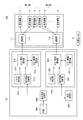
図1は、本発明を適用した実施形態に係る映像表示装置100の構成を示す図である。
この図1に示す映像表示装置100は、表示シート1(シート)と、光源ユニット2(光源)と、表示シート1及び光源ユニット2を制御する制御部10とを備えて構成される。
図1には表示シート1の外観を示す。表示シート1は矩形のシートであり、その表面に、多数の表示領域1aが、表示シート1の各辺に平行になるよう、マトリクス状に配置されている。
表示領域1aは、制御部10の制御により、後述するように表示シート1の内部に設けられた駆動用ピエゾ素子140(図4)等が駆動することで、外光を反射する反射率が変化する。各々の表示領域1aにおける反射率は、制御部10の制御によって独立して変化させることが可能である。そして、制御部10の制御により、複数の表示領域1aの反射率を個々に調整することで、表示シート1に、表示面から離れた空間に光干渉現象に基づく干渉縞を形成することができる。この干渉縞に光源ユニット2によって参照光を照射すれば、ホログラムが投影される。
Hereinafter, embodiments of the present invention will be described with reference to the drawings.
FIG. 1 is a diagram showing a configuration of a
The
FIG. 1 shows the appearance of the display sheet 1. The display sheet 1 is a rectangular sheet, and on its surface, a large number of
The
表示シート1のほぼ全面に並べて設けられた表示領域1aは、複数の群に割り当てられている。本実施形態では一例として、2つの群(第1群、第2群)に割り当てた場合について説明する。
表示シート1においては、表示シート1の短辺方向(図1中横方向)に延びる複数の帯状領域1b(帯状の領域)が設定される。各々の帯状領域1bは、縦横に並ぶ多数の表示領域1aを含んでおり、帯状領域1b全体では矩形である。そして、これら複数の帯状領域1bは表示シート1の長辺方向(図1中縦方向)に並んでおり、第1群に属する帯状領域1bと、第2群に属する帯状領域1bとが交互に並んでいる。また、第1群に属する帯状領域1bの数と第2群に属する帯状領域1bの数とは同数となっている。
The
In the display sheet 1, a plurality of band-
制御部10は、後述するように個々の表示領域1aの反射率を変化させることにより、帯状領域1bに干渉縞を形成する。表示領域1aは、ファブリ・ペロー干渉による光干渉効果によって、所定波長の外光を反射するよう構成され、少なくとも、反射率が高い状態と、反射率が非常に低い状態との2つの状態を切り替え可能である。また、表示領域1aの反射率を多段階で変化させる構成としてもよい。
表示シート1において、上記の干渉縞は群毎に形成される。すなわち、一つの群を構成する帯状領域1b全体を使って、一つの画像のホログラムを投影するための干渉縞が形成される。
表示シート1の周縁には選択回路11が設けられ、制御部10は選択回路11に接続されている。選択回路11は、制御部10の制御に従って、表示シート1に設けられた多数の表示領域1aの中から、特定の表示領域1aを選択する回路であり、制御部10は、選択回路11により選択された表示領域1aの反射率を調整する。
As will be described later, the
In the display sheet 1, the interference fringes are formed for each group. That is, interference fringes for projecting a hologram of one image are formed using the entire band-
A
制御部10は、表示シート1に設けられた表示領域1aの反射率を、群毎に調整する。すなわち、制御部10は、選択回路11によって表示領域1aを選択して反射率を調整する動作を、第1群に属する帯状領域1bを構成する全ての表示領域1aに対して行う。これにより、制御部10は、第1群に属する帯状領域1bに一つの画像を表示する。
第1群に属する帯状領域1bは、図1に示すように隙間をあけて表示シート1の全体に配置されているので、この多数の帯状領域1bに一つの画像を表示すれば、いわゆるインターレース表示と同様に、違和感なく表示シート1の全体に画像が表示されたように見える。
The
The band-
また、制御部10は、制御対象の群を第1群から第2群に切り替えることもできる。すなわち、制御部10は、選択回路11によって表示領域1aを選択して反射率を調整する動作を、第2群に属する帯状領域1bを構成する全ての表示領域1aに対して行う。これにより、制御部10は、第2群に属する帯状領域1bに一つの画像を表示する。
第1群と同様、第2群に属する帯状領域1bは、図1に示すように隙間をあけて表示シート1の全体に配置されているので、この多数の帯状領域1bに一つの画像を表示すれば、いわゆるインターレース表示と同様に、違和感なく表示シート1の全体に画像が表示されたように見える。
The
Similar to the first group, the band-
このように、表示シート1の構成では、第1群、第2群のいずれを用いても、表示シート1の全体に画像が表示されるように見せることが可能である。
そこで、映像表示装置100は、第1群を用いた表示と第2群を用いた表示とを交互に行うことで、動画像を表示する。
すなわち、映像表示装置100は、図示しない外部の装置から映像データ(例えば、30フレーム/秒)が入力された場合に、この映像データを構成する各フレームの画像を抽出し、連続するフレームの画像を第1群と第2群によって交互に表示する。この例では、第1群の帯状領域1bには毎秒15回の表示が行われ、第2群も同様である。これにより、帯状領域1bの各表示領域1aの表示状態を調整するために必要な時間が、映像データのフレームレート(この例では30フレーム/秒)の半分(15フレーム/秒)となるので、表示領域1aの表示状態の調整に必要な時間を確保しながら、表示シート1全体では30フレーム/秒の滑らかな表示を行うことができる。
As described above, in the configuration of the display sheet 1, it is possible to make it appear that an image is displayed on the entire display sheet 1 regardless of whether the first group or the second group is used.
Therefore, the
That is, when video data (for example, 30 frames / second) is input from an external device (not shown), the
映像表示装置100は、表示シート1に画像そのものを表示するものではなく、各表示領域1aにおける反射率を調整することにより、ホログラムを構成する干渉縞を形成する。表示シート1の全体に干渉縞を形成する処理は、後述するように圧電体に電界を印加して変形させる動作であるから高速に実行可能であるが、それでも、ある程度の時間を要すると考えられる。映像表示装置100は、映像を構成する複数のフレームに対応する干渉縞を、複数の群の帯状領域1bを切り替えながら形成することで、短時間に多数の干渉縞を形成し、高フレームレートの滑らかな映像(動画像)のホログラムを実現できる。
The
光源ユニット2は、コヒーレント光を表示シート1に向けて照射する光源であり、本実施形態では一例として、レーザー光源21を備え、このレーザー光源21から発した参照光22を、表示シート1の任意の領域に照射する。
光源ユニット2は、制御部10に接続され、制御部10によって照射開始/停止のタイミング、及び、表示シート1における被照射範囲が制御される。光源ユニット2は、表示シート1に構成された各々の表示領域1aを走査して、各表示領域1aに順次参照光22を照射することが可能である。
制御部10は、光源ユニット2を制御して、第1群の帯状領域1bを走査する動作と、第2群の帯状領域1bを走査する動作とを、帯状領域1bに干渉縞を形成するタイミングに合わせて実行する。詳細には、第1群の帯状領域1bに干渉縞が形成された後、制御部10は、第1群の帯状領域1bを構成する表示領域1aを走査するように光源ユニット2から参照光22を照射させる。この間、制御部10は、第2群の帯状領域1bに干渉縞を形成する動作を実行する。そして、第2群の帯状領域1bへの干渉縞の形成が完了したら、制御部10は光源ユニット2を制御して第2群の帯状領域1bに参照光22を照射させる。このように干渉縞の形成と参照光22の照射とを、第1群と第2群とを交互に切り替えながら連続して実行することで、制御部10は、表示シート1によって次々とホログラムを投影し、ホログラムによる立体映像を表示する。
The
The
The
図2は、映像表示装置100の構成を示す機能ブロック図である。
上述したように、表示シート1は、表示シート1に設けられた多数の表示領域1aの中から、特定の表示領域1aを選択する選択回路11を備えている。ここで、各々の表示領域1aは第1群または第2群のいずれかに割り当てられており、群ごとに制御される。このため、選択回路11は、第1群に属する表示領域1aの中から特定の表示領域1aを選択する選択部11aと、第2群に属する表示領域1aの中から特定の表示領域1aを選択する選択部11bとを備えている。
FIG. 2 is a functional block diagram showing the configuration of the
As described above, the display sheet 1 includes the
制御部10は、選択部11aに接続された第1制御部210と、選択部11bに接続された第2制御部220とを備える。
制御部10は、外部の装置(図示略)に接続される外部インターフェース(I/F)201と、外部インターフェース201を介して入力された映像データを処理して一画面分の画像データを生成し、生成した画像データを第1制御部210と第2制御部220との各々に出力する表示情報処理部202とを備えている。
より詳細には、表示情報処理部202は、入力された映像データを構成するフレームを抽出し、各フレームを構成する一画面分の画像データを生成する。この画像データは、例えば、映像データのフレームを切り出し、解像度を表示シート1における表示領域1aの数に合わせて変換したデータである。また、表示情報処理部202は、入力された画像データがフルカラーのデータであった場合、抽出したフレームのデータを2値のデータあるいはグレースケールのデータに変換(減色)して、第1制御部210、第2制御部220に出力する。
The
The
More specifically, the display
第1制御部210は、表示領域1aを駆動するためのパルスを生成するパルス発生部211と、表示情報処理部202から入力された画像データを取得して、この画像データを構成する画素(ピクセル)を表示シート1における表示領域1aに割り当てる処理を行う表示情報供給部212と、を備えている。表示情報供給部212は、表示情報処理部202から入力された画像データに対応する干渉縞を、第1群を構成する全ての帯状領域1bを使って形成するために、各表示領域1aの反射状態を決定する。表示領域1aの反射状態は、例えば、上記のように2段階に切り替え可能であるため、表示情報供給部212は、入力された画像データから各々の表示領域1aの反射率を算出し、決定する。この表示情報供給部212により決定された各表示領域1aの反射率を示す情報は、パルス発生部211が生成したパルスとともにピエゾ信号発生部213に入力される。ここで、表示情報供給部212からピエゾ信号発生部213には、パルス発生部211が生成したパルスに同期して、各表示領域1aの反射率を示す情報が一つの表示領域1a毎に順次入力されてもよい。
The
ピエゾ信号発生部213は、パルス発生部211から入力されるパルスに従って、選択部11aに対して制御信号を送出することにより、第1群の表示領域1aを順次選択させる。そして、ピエゾ信号発生部213は、選択部11aが選択している表示領域1aの反射率を、表示情報供給部212から入力される情報に従って制御する。
具体的には、ピエゾ信号発生部213には、表示領域1aの反射率を変化させるために表示領域1aに電界を印加するのに必要な電圧が、ピエゾ振動電圧部214から供給されている。ピエゾ信号発生部213は、選択部11aにより選択されている表示領域1aの反射率を、表示情報供給部212により決定された反射率にするため、ピエゾ振動電圧部214から供給される電圧をもとに表示領域1aに電界を印加する。
その後、ピエゾ信号発生部213は、パルス発生部211から入力されるパルスに同期したタイミングで選択部11aを制御し、次の表示領域1aを選択させ、新たに選択された表示領域1aの反射率を、表示情報供給部212により決定された反射率にするため電界を印加する。以上の動作を、第1群の帯状領域1bを構成する全ての表示領域1aに対して行うことで、一つの画像データに対応する干渉縞が形成される。
The
Specifically, a voltage necessary for applying an electric field to the
Thereafter, the piezo
また、第2制御部220は、第1制御部210と同様に構成される。
第2制御部220は、パルス発生部211と同様に表示領域1aを駆動するためのパルスを生成するパルス発生部221と、表示情報供給部212と同様に、表示情報処理部202から入力された画像データを取得して、この画像データを構成する画素を表示シート1における表示領域1aに割り当てる処理を行う表示情報供給部222と、を備えている。表示情報供給部222は、表示情報処理部202から入力された画像データに対応する干渉縞を、第2群を構成する全ての帯状領域1bを使って形成するため、各表示領域1aの反射状態を決定する。表示領域1aの反射状態は、例えば、上記のように2段階に切り替え可能であるため、表示情報供給部222は、入力された画像データから各々の表示領域1aの反射率を算出し、決定する。表示情報供給部222により決定された各表示領域1aの反射率を示す情報は、パルス発生部221が生成したパルスとともにピエゾ信号発生部223に入力される。ここで、表示情報供給部222からピエゾ信号発生部223には、パルス発生部221が生成したパルスに同期して、各表示領域1aの反射率を示す情報が一つの表示領域1a毎に順次入力されてもよい。
The
The
ピエゾ信号発生部223は、ピエゾ信号発生部213と同様、パルス発生部221から入力されるパルスに従って、選択部11bに対して制御信号を送出することにより、第1群の表示領域1aを順次選択させる。そして、ピエゾ信号発生部223は、選択部11bが選択している表示領域1aの反射率を、表示情報供給部222から入力される情報に従って制御する。
具体的には、ピエゾ信号発生部223には、表示領域1aの反射率を変化させるために表示領域1aに電界を印加するのに必要な電圧が、ピエゾ振動電圧部224から供給されている。ピエゾ信号発生部223は、選択部11bにより選択されている表示領域1aの反射率を、表示情報供給部222により決定された反射率にするため、ピエゾ振動電圧部224から供給される電圧をもとに表示領域1aに電界を印加する。
その後、ピエゾ信号発生部223は、パルス発生部221から入力されるパルスに同期したタイミングで選択部11bを制御し、次の表示領域1aを選択させ、新たに選択された表示領域1aの反射率を、表示情報供給部212により決定された反射率にするため電界を印加する。以上の動作を、第2群の帯状領域1bを構成する全ての表示領域1aに対して行うことで、一つの画像データに対応する干渉縞が形成される。
The
Specifically, the
Thereafter, the piezo
さらに、制御部10は、光源ユニット2を制御する光源制御部203を備えている。光源制御部203は、表示情報処理部202が映像データから1フレーム分の画像データを生成し、この画像データを第1制御部210及び第2制御部220に出力するタイミングに基づいて、光源ユニット2が参照光22(図1)を照射する範囲を、第1群とするか第2群とするかを決定する。そして、光源制御部203は、光源ユニット2に制御情報を出力することで、第1制御部210及び第2制御部220がそれぞれ帯状領域1bに干渉縞を形成するタイミングで、光源ユニット2が参照光22を照射する範囲を切り替えさせる。光源ユニット2は、光源制御部203から入力される制御情報に従って、第1群を構成する帯状領域1b、或いは第2群を構成する帯状領域1bを走査するよう参照光22を照射する。
Furthermore, the
これにより、表示シート1が有する第1群の帯状領域1bと、第2群の帯状領域1bとに、交互に1フレーム分の画像データに対応する干渉縞が形成され、これら第1群の干渉縞と第2群の干渉縞とに交互に参照光22が照射されるので、表示シート1の前方には、映像データの各フレームのホログラムが順次投影され、結果、ホログラムを利用して立体映像を投影することができる。
Thereby, interference fringes corresponding to image data for one frame are alternately formed in the first group of
図3は、映像表示装置100の動作を示すフローチャートである。
この図3に示すように、映像表示装置100の制御部10は、まず、外部インターフェース201を介して映像データを取得し、この映像データを表示情報処理部202に入力する(ステップS11)。
制御部10は、表示情報処理部202によって、入力された映像データを構成する各フレームを抽出し、このうち先頭フレームを選択し(ステップS12)、さらに、表示対象の群(以下、表示群とする)として第1群を選択する(ステップS13)。
制御部10は、表示情報処理部202から第1制御部210または第2制御部220のうち表示群に対応する側に対し、映像データから抽出した1フレーム分の画像データを出力し、第1制御部210または第2制御部220によって、表示群の帯状領域1bに干渉縞を形成する(ステップS14)。また、制御部10は、光源制御部203の機能により光源ユニット2の照射範囲を切り替えさせ、表示群の帯状領域1bを走査するように参照光22を照射させる(ステップS15)。これにより、表示シート1に干渉縞が形成され、この干渉縞に参照光22が照射されて、ホログラムを利用した立体画像が投影される。
FIG. 3 is a flowchart showing the operation of the
As shown in FIG. 3, the
The
The
ここで、制御部10は、映像データの最終フレームまで投影したか否かを判別し(ステップS16)、まだ最終フレームまで投影していない場合(ステップS16;No)、映像データから抽出したフレームのうち次のフレームを選択し(ステップS17)、さらに、現在選択中の表示群とは別の群を表示群として選択し(ステップS18)、ステップS14に戻る。これにより、映像データを構成する複数のフレームが、表示群を切り替えながら順次立体画像として投影される。
そして、映像データの最終フレームまで投影されると(ステップS16;Yes)、制御部10は、本処理を終了する。
Here, the
When the video data is projected up to the final frame (step S16; Yes), the
なお、制御部10は、ステップS14で表示群の帯状領域1bに干渉縞を形成する際に、いったん全ての表示領域1aの反射率を、初期状態にリセットする動作を行ってもよい。この動作を行うことで、全ての表示領域1aが同一の状態となるので、その後に各表示領域1aの反射率を制御する動作において、それ以前の表示領域1aの状態を考慮する必要がなく、高速化及び効率化を図ることができるという利点がある。
In addition, when forming an interference fringe in the band-
続いて、映像表示装置100において干渉縞が形成される表示シート1の構成について詳細に説明する。
図4は表示シート1の構成を示す要部断面図である。
表示シート1は、可撓性を有するシートとして構成され、例えば図1に示すように屈曲させることも可能であり、折り曲げることもできる。表示シート1の縁には選択回路11が設けられ、この選択回路11に、表示シート1の表示状態を制御する制御部10が接続されている。
表示シート1の表面は、透光性を有する表面層150により覆われ、表示シート1の裏面側は可撓性を有するベースシート101で構成され、これらベースシート101と表面層150との間に各部を収めた構成となっている。
Next, the configuration of the display sheet 1 on which interference fringes are formed in the
FIG. 4 is a cross-sectional view of the main part showing the configuration of the display sheet 1.
The display sheet 1 is configured as a flexible sheet. For example, the display sheet 1 can be bent as shown in FIG. 1 or can be bent. A
The surface of the display sheet 1 is covered with a
表面層150は、透明または半透明の透光性を有する層であり、有色(白色を含む)または無色のいずれであってもよい。表面層150は、例えば合成樹脂により構成される。表面層150の下側、すなわちベースシート101側の面は平滑で高い反射率を有するハーフミラーとして機能し、下方から入射した光を反射する。
ベースシート101は、可撓性を有するとともに、後述する各部を支持可能な所定の引っ張り強度を有するシートである。ベースシート101の透明度は任意であるが、表示シート1の表面(表面層150側)の表示を妨げないように、不透明または半透明であることが好ましい。ベースシート101には、合成樹脂製のシート或いはガラス等の無機材料からなるシートを用いることができる。
なお、以下の説明においては、便宜上、表面層150側を上、ベースシート101側を下として説明する。勿論、表示シート1の使用時における表示シート1の設置状態や設置の向きは何ら制限されない。
The
The
In the following description, for the sake of convenience, the
ベースシート101の上側には、複数の分極用ピエゾ素子120が配置される。分極用ピエゾ素子120は、強誘電体(例えば、チタン酸ジルコン酸鉛、チタン酸バリウム等)で構成される板または膜或いは層である。分極用ピエゾ素子120は、下側に配置されたX方向配線111と、上側に配置されたY方向配線112とに接続されている。
A plurality of polarization
図5は、X方向配線111、Y方向配線112、分極用ピエゾ素子120及び駆動用ピエゾ素子140の配置状態を示す要部斜視図であり、図6は、分極用ピエゾ素子120と各配線の接続状態を示す要部平面図である。
図5及び図6に示すように、本実施形態の分極用ピエゾ素子120は、正方形に形成され、表示シート1のほぼ全面に、縦方向及び横方向に所定間隔をあけてマトリクス状に並んでいる。
分極用ピエゾ素子120の下側には、表示シート1の幅方向に延びるX方向配線111が配置されている。X方向配線111は金属やカーボン等の導体材料からなる膜或いは層であり、分極用ピエゾ素子120に電気的に接続されている。X方向配線111は、所定間隔をあけて並ぶ分極用ピエゾ素子120に対応して、表示シート1の長手方向に平行に並べて複数設けられている。1本のX方向配線111には、X方向配線111に沿って一列に並ぶ複数の分極用ピエゾ素子120が接続されている。
FIG. 5 is a main part perspective view showing the arrangement state of the
As shown in FIGS. 5 and 6, the polarization
An
また、分極用ピエゾ素子120の上側には、表示シート1の長手方向に延びるY方向配線112が、表示シート1の幅方向に並べて配置されている。Y方向配線112はX方向配線111と同様、金属やカーボン等の導体材料からなる薄膜であり、分極用ピエゾ素子120に電気的に接続されている。Y方向配線112は、所定間隔をあけて並ぶ分極用ピエゾ素子120に対応して、表示シート1の幅方向に平行に並べて複数設けられている。1本のY方向配線112には、Y方向配線112に沿って一列に並ぶ複数の分極用ピエゾ素子120が接続されている。
Y方向配線112は、X方向配線111及び後述する透明配線113とともに、配線部110を構成する。
ここで、X方向配線111及びY方向配線112は、保持用配線部を構成し、Y方向配線112及び透明配線113は駆動用配線部を構成する。
Further, Y-
The
Here, the
全てのX方向配線111及びY方向配線112は、それぞれ選択回路11(図1)に接続されている。
選択回路11は、制御部10の制御に従って、複数のX方向配線111の中から1または複数のX方向配線111を選択し、選択したX方向配線111を制御部10に接続する。また、選択回路11は、複数のY方向配線112の中から1または複数のY方向配線112を選択し、選択したY方向配線112を制御部10に接続する。制御部10は、選択回路11により選択されたX方向配線111、Y方向配線112の電位を制御し、X方向配線111とY方向配線112との間に電圧を印加する。
All the X direction wirings 111 and the Y direction wirings 112 are respectively connected to the selection circuit 11 (FIG. 1).
The
図4に示すように、分極用ピエゾ素子120の下側に位置するX方向配線111と表面層150との間には、絶縁層131が配されている。絶縁層131は、絶縁性を有する合成樹脂等であり、X方向配線111とX方向配線111との間、及び、X方向配線111と表面層150との間の空間を満たしており、X方向配線111や分極用ピエゾ素子120と表面層150とを絶縁及び保護する役目がある。
絶縁層131の色について特に制限は無いが、例えば遮光性を有する材料を用いた場合には、表面層150から余分な反射光が放射されるのを防ぐことができる。すなわち、後述する駆動用ピエゾ素子140は透光性の材料であっても遮光性の材料であっても良いが、透光性の材料を用いた場合、表面層150から入射した光が駆動用ピエゾ素子の下方に位置するX方向配線111に達し、このX方向配線111で反射する可能性がある。ここで、絶縁層131が遮光性を有する材料、或いは、透光性の低い材料で構成されている場合、X方向配線111に外光が殆ど達しない上、X方向配線111の反射光が表面層150へ放射されないので、駆動用ピエゾ素子140の動作に関係なく放射される余分な放射光を防止できるという利点がある。
As shown in FIG. 4, an insulating
Although there is no particular limitation on the color of the insulating
分極用ピエゾ素子120の上方には、駆動用ピエゾ素子140(圧電体)が、分極用ピエゾ素子120に対応するようにマトリクス状に並べて配置されている。
一つの駆動用ピエゾ素子140は、一つの表示領域1a(図1)に相当する。
駆動用ピエゾ素子140は、圧電体で構成され、例えば、チタン酸ジルコン酸鉛、チタン酸バリウム、ニオブ酸リチウム、タンタル酸リチウム等の無機圧電体材料、或いは、ポリフッ化ビニリデン等の有機圧電体材料で構成される板または膜或いは層である。図5に示すように、本実施形態の駆動用ピエゾ素子140は、正方形に形成され、表示シート1の縦方向及び横方向に所定間隔をあけてマトリクス状に並んでいる。
Above the piezo element for
One driving
The driving
駆動用ピエゾ素子140の上面には、透明配線113が敷設されている。透明配線113は、酸化インジウムスズ(Indium Tin Oxide)や、酸化亜鉛系透明導電材料、水酸化マグネシウム−炭素系透明導電材料等の、透光性を有する導体の膜(層)で構成されている。透明配線113は、所定間隔を開けて並ぶ駆動用ピエゾ素子140に対応して、例えばX方向配線111と同じく表示シート1の幅方向に延びるように、平行に並べて複数設けられている。全ての透明配線113は選択回路11(図1)に接続され、これら複数の透明配線113の中から任意の1本を、選択回路11によって選択できる。
透明配線113はX方向配線111と同方向に並べて配設されているので、1本の透明配線113と1本のY方向配線112とが選択されると、その交差する場所に位置する一つの駆動用ピエゾ素子140が特定される。選択回路11(図1)は、制御部10の制御に従って1または複数の透明配線113を選択し、選択した透明配線113を制御部10に接続する。制御部10は、選択回路11により接続された透明配線113を接地させる。
Since the
隣接する駆動用ピエゾ素子140と駆動用ピエゾ素子140との間には、スペーサー141が配設されている。スペーサー141の厚みは、合成樹脂等の絶縁材料で構成され、電界が印加されていない状態の駆動用ピエゾ素子140と透明配線113とを合わせた厚みに相当し、駆動用ピエゾ素子140、透明配線113及びスペーサー141が一つの層を形成している。この層とY方向配線112との間、及び、Y方向配線112とY方向配線112との間に形成される空間は、絶縁層132により満たされている。絶縁層132は、絶縁層131と同様に構成される絶縁体の層である。また、スペーサー141は隣り合う透明配線113の間も区分する。
A
駆動用ピエゾ素子140の上方には、透明配線113の上に誘電体ミラー142が設けられている。誘電体ミラー142は、1層または多層の誘電体の膜で構成され、ハーフミラーとして機能する。すなわち、誘電体ミラー142は、表面層150を通して表示シート1内部に入射した外光を表面層150へ反射する。本実施形態の誘電体ミラー142はアルミニウムで構成されており、酸化防止のため、誘電体ミラー142の上面(表面)は酸化膜143により覆われている。
A
誘電体ミラー142と表面層150の下面は、いずれもハーフミラーであるため、これらの2つの面のファブリ・ペロー干渉の干渉効果により、外部から表面層150を透過して入射した光のうち特定の波長の光が、反射光として外部に放射される。つまり、誘電体ミラー142は表面層150と組み合わされて反射層を構成し、入射光に含まれる所定波長の光を反射する。ここで、反射される光の波長は、誘電体ミラー142と表面層150との間の空間144の厚み(ギャップ)によって決まるので、表示シート1により表示する色の波長に合わせて上記ギャップの大きさが予め設定されている。本実施形態では、ギャップの大きさは、光源ユニット2から照射される参照光22の波長に合わせて設定されている。
Since both the lower surface of the
誘電体ミラー142の下面(裏面)は、透明配線113に密着しており、透明配線113は駆動用ピエゾ素子140の上面に固定されている。このため、後述するように駆動用ピエゾ素子140が変形すると、駆動用ピエゾ素子140の変形に伴って透明配線113とともに誘電体ミラー142が変位し、誘電体ミラー142と表面層150との間のギャップが拡大する。ギャップが拡大すると、誘電体ミラー142における反射率が著しく低下するので、この位置では表示シート1の表面への反射光がほぼ無くなる。これを表示シート1の表面側から見れば、所定波長の光を反射する部分と、殆ど反射しない部分とが存在するので、各部分を制御することによって所定の色で画像を表示できる。
以下、駆動用ピエゾ素子140を変形させる動作について説明する。
The lower surface (back surface) of the
Hereinafter, an operation of deforming the driving
図5に示すように、一つの駆動用ピエゾ素子140に対しては1本のY方向配線112と1本の透明配線113とが接続されているので、選択回路11によって1本ずつY方向配線112と透明配線113とを選択することで、この1組のY方向配線112、透明配線113に接続された唯一の駆動用ピエゾ素子140を選択できる。従って、選択回路11によって一組のY方向配線112、透明配線113を選択して制御部10に接続し、制御部10においてY方向配線112に正又は負の電圧を印加するとともに透明配線113を接地させると、特定の駆動用ピエゾ素子140に対して電界が印加される。この駆動用ピエゾ素子140はY方向配線112と透明配線113との間の電界を受けて変形する。
As shown in FIG. 5, since one Y-
図7は、駆動用ピエゾ素子140の変形(駆動)の様子を説明する図である。図7(A)は駆動用ピエゾ素子140の非駆動時を示す駆動用ピエゾ素子140近傍の要部断面図であり、図7(B)は駆動時における要部断面図である。
Y方向配線112と透明配線113との間に電界が印加されていない状態では、図7(A)に示すように、駆動用ピエゾ素子140は透明配線113とともにスペーサー141と同じ厚みを保持している。この場合の、表面層150の下面と誘電体ミラー142とのギャップは予め設定された値d1である。
ここで、Y方向配線112と透明配線113との間に電界が印加されると、図7(B)に示すように、駆動用ピエゾ素子140が厚み方向に変形し、この変形に伴って誘電体ミラー142が下方に変位する。この状態における表面層150の下面と誘電体ミラー142とのギャップは拡大し、最も大きい場所で、図中d2で示す大きさになる。
FIG. 7 is a diagram for explaining a state of deformation (drive) of the driving
In a state where no electric field is applied between the Y-
Here, when an electric field is applied between the Y-
図7(B)に示すようにギャップが拡大した場合、誘電体ミラー142における反射率が低下し、外光が吸収されるため、表面層150から放射される反射光の光量が低減する。従って、駆動用ピエゾ素子140に電界を印加するか否かに応じて反射光の光量を大きく異ならせることができるので、表示シート1を表面側から見た場合に所定色の光を反射する部分と暗い部分とを混在させることができ、表示シート1全体で画像を表示できる。
このように、表示シート1は、ファブリ・ペロー干渉による光干渉効果により、入射光に含まれる所定波長の光を反射する機能を備え、一部の駆動用ピエゾ素子140に電界を印加して変形させることにより、駆動用ピエゾ素子140の位置毎に反射光を変化させて、反射光の強弱或いは有無による表示を行える。この場合、各々の駆動用ピエゾ素子140は表示単位(いわゆる画素)として機能し、外光(参照光)を利用して、表示シート1に文字や画像等を自在に表示できる。
When the gap is widened as shown in FIG. 7B, the reflectance of the
As described above, the display sheet 1 has a function of reflecting light having a predetermined wavelength included in incident light due to a light interference effect due to Fabry-Perot interference, and is deformed by applying an electric field to some driving
ここで、駆動用ピエゾ素子140に対して電界を印加した場合、駆動用ピエゾ素子140は透明配線113及びY方向配線112と静電結合するので、Y方向配線112及び透明配線113は駆動用ピエゾ素子140に対して電気的に直接接続されている必要はない。また、駆動用ピエゾ素子140に対して直接電圧を印加する場合には、Y方向配線112及び透明配線113を駆動用ピエゾ素子140に電気的に接続した構成とすればよい。
Here, when an electric field is applied to the driving
また、図5に示すように、一つの分極用ピエゾ素子120に対しては1本のX方向配線111と1本のY方向配線112とが接続されているので、1本のX方向配線111と1本のY方向配線112とを選択した場合、この1組のX方向配線111、Y方向配線112に接続された唯一の分極用ピエゾ素子120に対して、X方向配線111及びY方向配線112を介して電圧を印加することができる。
分極用ピエゾ素子120は強誘電体で構成されるから、X方向配線111とY方向配線112とに電圧を印加すると、分極用ピエゾ素子120に分極が生じる。例えば、X方向配線111を低電圧側とし、Y方向配線112を高電圧側として、分極用ピエゾ素子120に電圧を印加すると、分極が生じて分極用ピエゾ素子120の上面に負電荷が局在し、分極用ピエゾ素子120の下面に正電荷が局在した状態となる。
Also, as shown in FIG. 5, since one
Since the polarization
図5に示すように、一つの分極用ピエゾ素子120の真上には一つの駆動用ピエゾ素子140が位置しているから、分極用ピエゾ素子120に分極が生じると、その真上の駆動用ピエゾ素子140が分極用ピエゾ素子120の表面の電荷の影響を受ける。例えば、分極用ピエゾ素子120の上面に負電荷が局在する場合、駆動用ピエゾ素子140の周囲には透明配線113から分極用ピエゾ素子120に向かう電界が生じる。このとき透明配線113が制御部10によって接地されていれば、より強い電界が生じる。そして、分極用ピエゾ素子120の電荷により生じた電界の影響で、圧電体である駆動用ピエゾ素子140は変形する。
また、Y方向配線112に電圧を印加して駆動用ピエゾ素子140を変形させた状態で、分極用ピエゾ素子120の電荷により電界が生じた場合、駆動用ピエゾ素子140は、分極用ピエゾ素子120の電荷によって変形した状態を保つ。このため、Y方向配線112への電圧の印加を止めても、駆動用ピエゾ素子140が変形したままになる。
As shown in FIG. 5, since one driving
When an electric field is generated by the electric charge of the polarization
制御部10(図2)の第1制御部210及び第2制御部220が、選択部11a、11bにより選択した表示領域1aの反射率を調整する動作は、以下の通りである。
まず、対象の表示領域1aの駆動用ピエゾ素子140に繋がる一組のY方向配線112及び透明配線113を、選択部11a、11bによって選択させる。
対象の表示領域1aにおける反射率を低下させる場合、制御部10は、選択されたY方向配線112及び透明配線113の間に、ピエゾ振動電圧部214、224から供給される電圧により、電界を印加する。これにより、駆動用ピエゾ素子140に電界が印加されて変形し、表示領域1aにおける反射率が低い状態となる。
続いて、制御部10は、選択部11a、11bにより、選択中の駆動用ピエゾ素子140の直下に位置する分極用ピエゾ素子120に繋がるX方向配線111を選択させ、このX方向配線111と、先に選択したY方向配線112との間に電圧を印加する。これにより、変形した駆動用ピエゾ素子140の直下の分極用ピエゾ素子120が分極して、駆動用ピエゾ素子140の変形を保持できるようになる。
このように、制御部10の第1制御部210は、選択部11aによって第1群の表示領域1aの各々を、反射率の高い状態と、反射率の低い状態とのどちらにも自在に切り替えることができる。
The operation in which the
First, a pair of Y-
When reducing the reflectance in the
Subsequently, the
As described above, the
なお、制御部10は、上述したように、第1群または第2群の帯状領域1bに干渉縞を形成する際に、いったん全ての表示領域1aの反射率を初期状態にリセットする動作を行ってもよい。この動作は、選択部11a或いは選択部11bによって、処理対象の群の表示領域1aに相当する分極用ピエゾ素子120に繋がるX方向配線111及びY方向配線112を順次選択し、このX方向配線111及びY方向配線112を介して、分極用ピエゾ素子120に蓄積されている電荷を放出させればよい。この動作を、対象の群を構成する全ての表示領域1aについて行えば、その群の表示領域1aの反射率は初期状態に戻る。
As described above, the
また、例えば、選択部11a、11bが、それぞれ、全てのX方向配線111及びY方向配線112を同時に選択する機能を備えた構成としてもよい。この場合、選択部11a、11bのうち、対象の群に接続された側において、全てのX方向配線111及びY方向配線112を選択して接地させると、その群の全ての表示領域1aに対応する分極用ピエゾ素子120の分極が解消する。この構成では、簡単かつ高速に、多くの表示領域1aを初期状態に戻すことができる。
この動作を行うことで、各表示領域1aの反射率を調整して干渉縞を形成する動作において、それ以前の表示領域1aの状態を考慮する必要がなく、高速化及び効率化を図ることができる。
For example, the
By performing this operation, in the operation of adjusting the reflectance of each
以上のように、本発明を適用した実施形態に係る映像表示装置100によれば、光波の干渉現象を正確に発生させるための物理的な構造体の特質を有する原理と同一の原理であるファブリ・ペロー干渉による光干渉効果によって所定波長の光を反射する機能を備えた表示シート1の表示領域1aを複数の群に分け、表示領域1aで構成される帯状領域1bに群毎に干渉縞を形成して、光源ユニット2から参照光を照射するので、複数の群を切り替えながら異なる立体画像を次々と投影することができ、一つの群によりホログラムを投影した後、他の群により別の画像のホログラムを投影することで、ホログラムを順次変化させて、ホログラムによる立体映像を表示できる。
この場合、第1群と第2群とを切り替えることにより、一つの群において干渉縞を形成する時間を長く確保できるので、高解像度化が容易である。第1群の帯状領域1bに参照光22を照射している間に、第2群の干渉縞を形成すればよいので、解像度を高めて干渉縞の形成に時間がかかったとしても、干渉縞の形成が追いつかないという事態が生じない。これにより、高解像度で緻密な干渉縞を形成できる。また、短い時間でホログラムを切り替えることが可能なため、高速にホログラムを変化させることができ、滑らかな立体映像を表示できる。特に、ホログラムは残像が残りやすい特性を有するので、先に投影したホログラムの残像を残しつつ次のホログラムを投影することで、より滑らかに変化する立体映像を表示・再生できる。さらに、干渉縞の形成自体を高速化する特別な仕組みを必要とせず、シンプルな構成によって容易に実現できる。特に、映像表示装置100は、可撓性を有する薄型の表示シート1を用いているため、設置場所の確保が容易であり、例えば壁掛け型としても、吊り下げ型としても、床面に立設された台座に固定してもよく、設置スペースはわずかで済むという利点がある。
As described above, according to the
In this case, by switching between the first group and the second group, it is possible to ensure a long time for forming the interference fringes in one group, so that it is easy to increase the resolution. Since the second group of interference fringes may be formed while the first group of strip-
また、制御部10により、一つの群の表示領域1aを用いて1フレームの画像を構成する干渉縞を形成する動作を、対象の群を切り替えながら連続して実行し、制御部10によって各群の表示領域1aに干渉縞が形成される毎に、光源ユニット2によって参照光を照射する群を切り替えるので、ホログラムを連続的にかつ高速に変化させることで、滑らかな立体映像の投影を可能とし、かつ、高解像度化が容易である。
また、表示シート1は矩形で構成され、この矩形の表示シート1において、複数の表示領域1aは表示シート1の一辺に沿って並ぶ複数の帯状領域1bに分けられ、各群は複数の帯状領域1bによって構成され、帯状領域1bは、異なる群を構成する帯状領域1bが隣り合うよう配置された構成であるため、第1群、第2群のいずれにおいても、表示シート1全体とほぼ同じサイズの干渉縞を形成できるので、表示シート1の表示領域1aを効率よく使って、大きなサイズで緻密なホログラムを投影できる。また、群を切り替えた場合に干渉縞のサイズと位置とが殆ど変わらないため、群を切り替えた場合のホログラムの変化を微少な変化とすることができ、立体映像をより滑らかに変化させることができる。
In addition, the
Further, the display sheet 1 is configured in a rectangular shape. In the rectangular display sheet 1, the plurality of
また、駆動用ピエゾ素子140の変形量は、駆動用ピエゾ素子140に加わる電界の強度によって変化する。このため、駆動用ピエゾ素子140に印加する電界、分極用ピエゾ素子120に印加する電圧を調整することで、駆動用ピエゾ素子140の変形量を調整し、誘電体ミラー142により反射される光の反射率、或いは、誘電体ミラー142による反射と吸収を任意に変化させることができる。つまり、各表示領域1aにおける反射率を複数段階に異ならせて、階調表現を実現することも可能である。
Further, the amount of deformation of the driving
表示シート1は、分極用ピエゾ素子120に蓄積された電荷により駆動用ピエゾ素子140の変形を保持できるので、表示状態の保持に要する電力量が小さくて済み、給電しなくても長時間にわたって表示状態を保持できる。このため、制御部10によって形成された干渉縞を、外部から給電せずに長時間保持できる。また、一般に圧電体の変形は極めて迅速であるため、制御部10の制御により各表示領域1aの駆動用ピエゾ素子140が変形するまでの応答時間が非常に短い。このため、表示シート1に干渉縞を形成する処理も短時間で高速に実行できる。この表示シート1は、例えば、インクジェットプリンターと同様に構成される装置を用い、ベースシート101に対して、配線部110や分極用ピエゾ素子120、駆動用ピエゾ素子140等を構成する流体材料を噴射することにより、容易に低コストで製造可能である。
Since the display sheet 1 can hold the deformation of the driving
なお、上述した実施形態は本発明を適用した一態様を示すものであって、本発明は上記実施形態に限定されない。
上記実施形態では、表示シート1の表示領域1aを第1群と第2群とに分けた構成について説明したが、本発明はこれに限定されるものではなく、3以上の群に分けて、群ごとに干渉縞を形成してホログラムを投影することも勿論可能である。群が多くなれば、干渉縞の形成に要する時間に比べて著しく短い時間でホログラムを切り替えることが可能なため、より滑らかに変化する立体映像を実現できる。
また、上記実施形態では、矩形の表示シート1に、マトリクス状に矩形の表示領域1aを並べた構成を例に挙げて説明したが、本発明はこれに限定されるものではなく、表示領域1aの形状、及び、表示領域1aの配列状態は任意に変更可能である。例えば、六角形の表示領域1aをハニカム型の平面充填構造となるよう並べてもよいし、円形の表示領域1aを並べてもよい。この場合、表示領域1aどうしの間に隙間を生じても、この隙間から表示シート1の表側に光が漏れなければ、特に不都合はない。
In addition, embodiment mentioned above shows the one aspect | mode which applied this invention, Comprising: This invention is not limited to the said embodiment.
In the said embodiment, although the structure which divided | segmented the
Moreover, in the said embodiment, although the structure which arranged the rectangular display area |
また、上記実施形態では、分極用ピエゾ素子120を分極させることにより電荷を蓄積する構成としたが、分極用ピエゾ素子120に代えて、圧電体以外の材料を用いた電荷蓄積素子を形成し、この電荷蓄積素子に蓄積した電荷により駆動用ピエゾ素子140の周囲に電界を生成させてもよい。また、表示シート1は、表面層150と誘電体ミラー142との間のファブリ・ペロー干渉により特定波長の光を反射するものであればよいので、誘電体ミラー142に代えて、誘電体に該当しない材料によりハーフミラーを設けてもよい。さらに、表示シート1における分極用ピエゾ素子120、駆動用ピエゾ素子140の数や配置方向は任意であり、六角形の分極用ピエゾ素子120及び駆動用ピエゾ素子140をハニカム状に配置してもよいし、円形の分極用ピエゾ素子120、駆動用ピエゾ素子140を用いてもよい。隣接する駆動用ピエゾ素子140の間にスペーサー141を設けたように、分極用ピエゾ素子120どうしの間に絶縁体のスペーサーを設けてもよい。そして、表示シート1における表示色も任意であり、制御部10から表示シート1へ通電しておらず、全ての分極用ピエゾ素子120が分極していない状態における表示シート1の色は、白色であってもよいが、他の色であってもよく、その他の細部構成についても任意に変更可能である。
Further, in the above embodiment, the charge is accumulated by polarizing the polarization
1…表示シート(シート)、1a…表示領域、1b…帯状領域(帯状の領域)、2…光源ユニットI(光源)、10…制御部、11…選択回路、11a、11b…選択部、100…映像表示装置(表示装置)、140…駆動用ピエゾ素子(圧電体)、142…誘電体ミラー(反射層)、143…酸化膜、150…表面層(反射層)。
DESCRIPTION OF SYMBOLS 1 ... Display sheet (sheet | seat), 1a ... Display area, 1b ... Strip | belt-shaped area | region (band-shaped area | region), 2 ... Light source unit I (light source), 10 ... Control part, 11 ... Selection circuit, 11a, 11b ... Selection part, 100 DESCRIPTION OF SYMBOLS Image display apparatus (display apparatus) 140 ... Drive piezo element (piezoelectric body) 142 ... Dielectric mirror (reflection layer) 143 ...
Claims (4)
各表示領域は、外部から入射した光のファブリ・ペロー干渉による光干渉効果によって、入射光のうち所定波長の光を反射する反射層と、周囲の電界に応じて変形して前記反射層の反射率を変化させる圧電体と、を備えて構成され、
特定の前記表示領域に対応する前記圧電体を選択する選択部と、
前記選択部により特定の前記圧電体を選択させ、該圧電体に電界を加えて変形させることにより、前記反射層における反射率の差によって前記表示領域に干渉縞を形成させる制御部と、
前記表示領域に形成された干渉縞に参照光を照射する光源と、を備え、
複数の前記表示領域は複数の群に分けられており、前記制御部によって一つの群の表示領域を用いて一つの画像を構成する干渉縞を形成し、前記光源によって群毎に、表示領域に形成された干渉縞に参照光を照射すること、
を特徴とする表示装置。 A plurality of display areas for forming interference fringes are provided side by side on a flexible sheet,
Each display region has a reflection layer that reflects light of a predetermined wavelength of incident light due to a light interference effect of Fabry-Perot interference of light incident from outside, and a reflection layer that is deformed according to the surrounding electric field and reflected by the reflection layer. A piezoelectric body that changes the rate, and
A selection unit for selecting the piezoelectric body corresponding to the specific display area;
A control unit that causes the selection unit to select a specific piezoelectric body and deforms the piezoelectric body by applying an electric field, thereby forming interference fringes in the display region due to a difference in reflectance in the reflective layer;
A light source for irradiating reference light to the interference fringes formed in the display area,
The plurality of display areas are divided into a plurality of groups, and the control unit forms interference fringes constituting one image using the display areas of one group, and the light sources are arranged in the display areas for each group. Irradiating the formed interference fringes with reference light;
A display device.
前記制御部によって各群の表示領域に干渉縞が形成される毎に、前記光源によって参照光を照射する群を切り替えること、
を特徴とする請求項1記載の表示装置。 By the control unit, the operation of forming interference fringes constituting one image using the display area of one group is continuously executed while switching the target group,
Each time an interference fringe is formed in the display area of each group by the control unit, switching the group irradiated with the reference light by the light source,
The display device according to claim 1.
前記帯状の領域は、異なる群を構成する領域が隣り合うよう配置されたこと、
を特徴とする請求項1または2記載の表示装置。 The sheet is configured by a rectangle, and in the rectangular sheet, the plurality of display areas are divided into a plurality of band-shaped areas arranged along one side of the sheet, and each group is configured by a plurality of band-shaped areas,
The band-shaped region is arranged so that regions constituting different groups are adjacent to each other,
The display device according to claim 1 or 2.
各表示領域は、外部から入射した光のファブリ・ペロー干渉による光干渉効果によって、入射光のうち所定波長の光を反射する反射層と、周囲の電界に応じて変形して前記反射層の反射率を変化させる圧電体と、を備えて構成される表示装置を制御して、
特定の前記表示領域に対応する前記圧電体を選択し、選択した特定の前記圧電体に電界を加えて変形させることにより、前記反射層における反射率の差によって前記表示領域に干渉縞を形成させ、
複数の前記表示領域を複数の群に分け、一つの群の表示領域を用いて一つの画像を構成する干渉縞を形成し、群毎に、表示領域に形成された干渉縞に光源から参照光を照射すること、
を特徴とする表示制御方法。 A plurality of display areas for forming interference fringes are provided side by side on a flexible sheet,
Each display region has a reflection layer that reflects light of a predetermined wavelength of incident light due to a light interference effect of Fabry-Perot interference of light incident from outside, and a reflection layer that is deformed according to the surrounding electric field and reflected by the reflection layer. Controlling a display device comprising a piezoelectric body that changes the rate,
By selecting the piezoelectric body corresponding to the specific display area and applying an electric field to the selected specific piezoelectric body to deform it, an interference fringe is formed in the display area due to a difference in reflectance in the reflective layer. ,
The plurality of display areas are divided into a plurality of groups, and interference fringes constituting one image are formed using the display areas of one group, and reference light from the light source is formed on the interference fringes formed in the display areas for each group. Irradiating,
A display control method characterized by the above.
Priority Applications (1)
| Application Number | Priority Date | Filing Date | Title |
|---|---|---|---|
| JP2009157540A JP2011013456A (en) | 2009-07-02 | 2009-07-02 | Display device and display control method |
Applications Claiming Priority (1)
| Application Number | Priority Date | Filing Date | Title |
|---|---|---|---|
| JP2009157540A JP2011013456A (en) | 2009-07-02 | 2009-07-02 | Display device and display control method |
Publications (1)
| Publication Number | Publication Date |
|---|---|
| JP2011013456A true JP2011013456A (en) | 2011-01-20 |
Family
ID=43592404
Family Applications (1)
| Application Number | Title | Priority Date | Filing Date |
|---|---|---|---|
| JP2009157540A Withdrawn JP2011013456A (en) | 2009-07-02 | 2009-07-02 | Display device and display control method |
Country Status (1)
| Country | Link |
|---|---|
| JP (1) | JP2011013456A (en) |
Cited By (1)
| Publication number | Priority date | Publication date | Assignee | Title |
|---|---|---|---|---|
| JP2015510605A (en) * | 2011-12-30 | 2015-04-09 | バイエル・マテリアルサイエンス・リミテッド・ライアビリティ・カンパニーBayer MaterialScience LLC | Interferometric spatial light modulator for digital hologram production |
-
2009
- 2009-07-02 JP JP2009157540A patent/JP2011013456A/en not_active Withdrawn
Cited By (1)
| Publication number | Priority date | Publication date | Assignee | Title |
|---|---|---|---|---|
| JP2015510605A (en) * | 2011-12-30 | 2015-04-09 | バイエル・マテリアルサイエンス・リミテッド・ライアビリティ・カンパニーBayer MaterialScience LLC | Interferometric spatial light modulator for digital hologram production |
Similar Documents
| Publication | Publication Date | Title |
|---|---|---|
| US20170351090A1 (en) | Head-up display device | |
| KR100834415B1 (en) | Display device using microlens | |
| US20160349524A1 (en) | Multi-view display device | |
| US7746527B2 (en) | Optical scanning device using modulated laser beams control method of optical scanning device using modulated laser beams, and image display apparatus using modulated laser beams, the system including respective gradation of each pixel by the light beams and successively illuminating each pixel of the plurality of pixels | |
| JP2015509210A (en) | Optical imaging system and 3D display device | |
| WO2013029667A1 (en) | A device and method for projecting an image | |
| KR20110025922A (en) | Space display device | |
| JP2008310260A (en) | Image projection method and screen used for the method | |
| CN115981026B (en) | A three-dimensional display without crosstalk grating | |
| JP5083452B2 (en) | Optical scanning device, optical scanning device control method, and image display device | |
| US11487324B2 (en) | Display device, control method therefor, and head-mounted virtual display device | |
| CN110171136B (en) | High-efficiency line scanning photo-curing imaging device and method | |
| EP1707013A1 (en) | Volumetric display | |
| JP2008076973A (en) | Projector screen and projector | |
| JPH10161061A (en) | Stereoscopic video display device | |
| JP2011013456A (en) | Display device and display control method | |
| EP2453289B1 (en) | Diffractive optical nano-electro-mechanical device with reduced driving voltage | |
| JP7131209B2 (en) | Display device, display method and program | |
| EP3502765A1 (en) | Image display device | |
| JP2002328333A (en) | Wave front control type display device and image pickup and reproducing method | |
| JP2004102213A (en) | Optical scanning device | |
| JP5318014B2 (en) | 3D display device | |
| JP3804821B2 (en) | Light modulation device and projection system | |
| CN105093774A (en) | MEMS micro-mirror, display panel and display device | |
| CN210309079U (en) | High-efficient line scanning photocuring image device |
Legal Events
| Date | Code | Title | Description |
|---|---|---|---|
| A300 | Withdrawal of application because of no request for examination |
Free format text: JAPANESE INTERMEDIATE CODE: A300 Effective date: 20120904 |