JP2010171810A - Oscillation circuit - Google Patents
Oscillation circuit Download PDFInfo
- Publication number
- JP2010171810A JP2010171810A JP2009013388A JP2009013388A JP2010171810A JP 2010171810 A JP2010171810 A JP 2010171810A JP 2009013388 A JP2009013388 A JP 2009013388A JP 2009013388 A JP2009013388 A JP 2009013388A JP 2010171810 A JP2010171810 A JP 2010171810A
- Authority
- JP
- Japan
- Prior art keywords
- circuit
- node
- excitation circuit
- signal
- excitation
- Prior art date
- Legal status (The legal status is an assumption and is not a legal conclusion. Google has not performed a legal analysis and makes no representation as to the accuracy of the status listed.)
- Pending
Links
- 230000010355 oscillation Effects 0.000 title claims abstract description 110
- 230000005284 excitation Effects 0.000 claims abstract description 128
- 239000000872 buffer Substances 0.000 claims description 34
- 230000003321 amplification Effects 0.000 claims description 21
- 238000003199 nucleic acid amplification method Methods 0.000 claims description 21
- 239000003990 capacitor Substances 0.000 abstract description 14
- 238000010586 diagram Methods 0.000 description 24
- 239000013078 crystal Substances 0.000 description 14
- 230000004913 activation Effects 0.000 description 6
- 238000005259 measurement Methods 0.000 description 6
- 239000000919 ceramic Substances 0.000 description 5
- 230000001965 increasing effect Effects 0.000 description 5
- 230000000052 comparative effect Effects 0.000 description 4
- 230000000694 effects Effects 0.000 description 3
- 238000002474 experimental method Methods 0.000 description 3
- 230000010354 integration Effects 0.000 description 3
- 238000004904 shortening Methods 0.000 description 3
- 230000008859 change Effects 0.000 description 2
- 229910044991 metal oxide Inorganic materials 0.000 description 2
- 150000004706 metal oxides Chemical class 0.000 description 2
- 238000000034 method Methods 0.000 description 2
- 239000004065 semiconductor Substances 0.000 description 2
- 238000007493 shaping process Methods 0.000 description 2
- 230000000295 complement effect Effects 0.000 description 1
- 230000001939 inductive effect Effects 0.000 description 1
- 238000012986 modification Methods 0.000 description 1
- 230000004048 modification Effects 0.000 description 1
- 238000012544 monitoring process Methods 0.000 description 1
- 230000004044 response Effects 0.000 description 1
Images


Classifications
-
- H—ELECTRICITY
- H03—ELECTRONIC CIRCUITRY
- H03B—GENERATION OF OSCILLATIONS, DIRECTLY OR BY FREQUENCY-CHANGING, BY CIRCUITS EMPLOYING ACTIVE ELEMENTS WHICH OPERATE IN A NON-SWITCHING MANNER; GENERATION OF NOISE BY SUCH CIRCUITS
- H03B5/00—Generation of oscillations using amplifier with regenerative feedback from output to input
- H03B5/30—Generation of oscillations using amplifier with regenerative feedback from output to input with frequency-determining element being electromechanical resonator
- H03B5/32—Generation of oscillations using amplifier with regenerative feedback from output to input with frequency-determining element being electromechanical resonator being a piezoelectric resonator
- H03B5/36—Generation of oscillations using amplifier with regenerative feedback from output to input with frequency-determining element being electromechanical resonator being a piezoelectric resonator active element in amplifier being semiconductor device
Landscapes
- Oscillators With Electromechanical Resonators (AREA)
Abstract
Description
この発明は、水晶振動子やセラミック振動子などの圧電振動子を用いた発振回路に関する。 The present invention relates to an oscillation circuit using a piezoelectric vibrator such as a crystal vibrator or a ceramic vibrator.
従来の水晶発振回路は、PチャネルMOS(Metal-Oxide Semiconductor)トランジスタおよびNチャネルMOSトランジスタよりなるインバータの入力端子と出力端子との間に、水晶振動子、帰還抵抗素子、および容量素子を結合することによって、発振出力を得るものである。この水晶発振回路では発振周波数や振幅レベルの安定までに時間がかかるという問題がある。 In a conventional crystal oscillation circuit, a crystal resonator, a feedback resistor element, and a capacitor element are coupled between an input terminal and an output terminal of an inverter composed of a P-channel MOS (Metal-Oxide Semiconductor) transistor and an N-channel MOS transistor. Thus, an oscillation output is obtained. This crystal oscillation circuit has a problem that it takes time to stabilize the oscillation frequency and amplitude level.
この問題に関して、たとえば、特公平5−6362号公報(特許文献1)に記載される水晶発振回路が知られている。この発振回路は、1つの水晶振動子を共用する2組の水晶発振回路を有し、一方の水晶発振回路で振動状態にある水晶振動子を、他方の水晶発振回路に切換接続して動作するようにしたものである。 With regard to this problem, for example, a crystal oscillation circuit described in Japanese Patent Publication No. 5-6362 (Patent Document 1) is known. This oscillation circuit has two sets of crystal oscillation circuits that share one crystal oscillator, and operates by switching the crystal oscillator that is in a vibration state in one crystal oscillation circuit to the other crystal oscillation circuit. It is what I did.
ところで、携帯電話機を始めとするバッテリ電源で駆動する電子機器では、バッテリを長持ちさせるために省電力化が求められている。このため、電子部品に供給されるクロック信号は間欠動作させることが望ましい。このような間欠動作では、圧電振動子(水晶振動子、セラミック振動子など)の停止状態から安定発振に至る時間を短縮することが必要になる。前述の特公平5−6362号公報(特許文献1)に記載の技術は、圧電振動子の停止状態から安定発振に至る起動時間の短縮について開示するものでない。 By the way, in an electronic device driven by a battery power source such as a mobile phone, power saving is required in order to make the battery last longer. For this reason, it is desirable to intermittently operate the clock signal supplied to the electronic component. In such intermittent operation, it is necessary to shorten the time from the stop state of the piezoelectric vibrator (a crystal vibrator, a ceramic vibrator, etc.) to the stable oscillation. The technique described in the above Japanese Patent Publication No. 5-6362 (Patent Document 1) does not disclose shortening of the start-up time from the stop state of the piezoelectric vibrator to the stable oscillation.
この発明の目的は、圧電振動子の停止状態から安定発振に至る起動時間を短縮することが可能な発振回路を提供することである。 An object of the present invention is to provide an oscillation circuit capable of shortening a startup time from a stop state of a piezoelectric vibrator to a stable oscillation.
この発明は要約すれば発振回路であって、圧電振動子と、抵抗素子と、第1および第2の容量素子と、第1の励振回路とを備える。圧電振動子は、第1および第2のノード間に設けられる。抵抗素子は、第1および第2のノード間に圧電振動子と並列に設けられる。第1の容量素子は、第1のノードと接地ノードとの間に設けられる。第2の容量素子は、第2のノードと接地ノードとの間に設けられる。第1の励振回路は、第1および第2のノード間に圧電振動子および抵抗素子の各々と並列に設けられ、第1のノードの信号を反転増幅して第2のノードに出力する。そして、第1の励振回路は、各々が増幅回路として用いられる従属接続された複数の論理素子を含む。 In summary, the present invention is an oscillation circuit, which includes a piezoelectric vibrator, a resistance element, first and second capacitance elements, and a first excitation circuit. The piezoelectric vibrator is provided between the first and second nodes. The resistance element is provided in parallel with the piezoelectric vibrator between the first and second nodes. The first capacitive element is provided between the first node and the ground node. The second capacitor element is provided between the second node and the ground node. The first excitation circuit is provided between the first and second nodes in parallel with each of the piezoelectric vibrator and the resistance element, and inverts and amplifies the signal of the first node and outputs the signal to the second node. The first excitation circuit includes a plurality of cascade-connected logic elements each used as an amplifier circuit.
好ましい実施の一形態において、発振回路は、タイマー回路と、第2の励振回路とをさらに備える。タイマー回路は、イネーブル信号が活性状態になったときから予め定める時間だけ活性状態になる制御信号を出力する。第2の励振回路は、第1および第2のノード間に圧電振動子、抵抗素子、および第1の励振回路の各々と並列に設けられ、第1のノードの信号を反転増幅して第2のノードに出力する。ここで、第2の励振回路の電力増幅率は、第1の励振回路の電力増幅率より小さい。そして、第2の励振回路は、イネーブル信号が非活性状態のとき一定の論理レベルの信号を出力し、イネーブル信号が活性状態のとき増幅回路として動作する論理素子を含む。さらに、第1の励振回路を構成する複数の論理素子のうち初段および最終段の論理素子は、制御信号が非活性状態のとき高インピーダンス状態になる3ステートバッファである。 In a preferred embodiment, the oscillation circuit further includes a timer circuit and a second excitation circuit. The timer circuit outputs a control signal that is activated for a predetermined time from when the enable signal is activated. The second excitation circuit is provided between the first and second nodes in parallel with each of the piezoelectric vibrator, the resistance element, and the first excitation circuit, and inverts and amplifies the signal of the first node to generate the second excitation circuit. Output to the node. Here, the power amplification factor of the second excitation circuit is smaller than the power amplification factor of the first excitation circuit. The second excitation circuit includes a logic element that outputs a signal of a constant logic level when the enable signal is in an inactive state and operates as an amplifier circuit when the enable signal is in an active state. Further, among the plurality of logic elements constituting the first excitation circuit, the first and last stage logic elements are three-state buffers that are in a high impedance state when the control signal is in an inactive state.
好ましい実施の他の形態において、発振回路は、タイマー回路と、第1および第2のスイッチと、第2の励振回路とをさらに備える。タイマー回路は、イネーブル信号が活性状態になったときから予め定める時間だけ活性状態になる制御信号を出力する。第1のスイッチは、第1のノードと第1の励振回路の入力端との間に設けられ、制御信号が活性状態のときオン状態になり、制御信号が非活性状態のときオフ状態になる。第2のスイッチは、第2のノードと第1の励振回路の出力端との間に設けられ、制御信号が活性状態のときオン状態になり、制御信号が非活性状態のときオフ状態になる。第2の励振回路は、第1および第2のノード間に圧電振動子、抵抗素子、および第1の励振回路の各々と並列に設けられ、第1のノードの信号を反転増幅して第2のノードに出力する。ここで、第2の励振回路の電力増幅率は、第1の励振回路の電力増幅率より小さい。そして、第2の励振回路は、イネーブル信号が非活性状態のとき一定の論理レベルの信号を出力し、イネーブル信号が活性状態のとき増幅回路として動作する論理素子を含む。 In another embodiment of the preferred embodiment, the oscillation circuit further comprises a timer circuit, first and second switches, and a second excitation circuit. The timer circuit outputs a control signal that is activated for a predetermined time from when the enable signal is activated. The first switch is provided between the first node and the input end of the first excitation circuit, and is turned on when the control signal is in an active state and turned off when the control signal is in an inactive state. . The second switch is provided between the second node and the output terminal of the first excitation circuit, and is turned on when the control signal is active and turned off when the control signal is inactive. . The second excitation circuit is provided between the first and second nodes in parallel with each of the piezoelectric vibrator, the resistance element, and the first excitation circuit, and inverts and amplifies the signal of the first node to generate the second excitation circuit. Output to the node. Here, the power amplification factor of the second excitation circuit is smaller than the power amplification factor of the first excitation circuit. The second excitation circuit includes a logic element that outputs a signal of a constant logic level when the enable signal is in an inactive state and operates as an amplifier circuit when the enable signal is in an active state.
好ましい実施のさらに他の形態において、発振回路は、第2の励振回路と、タイマー回路と、第1および第2のスイッチとをさらに備える。第2の励振回路は、第1および第2のノード間に圧電振動子、抵抗素子、および第1の励振回路の各々と並列に設けられ、第1のノードの信号を反転増幅して第2のノードに出力する。ここで、第2の励振回路の電力増幅率は、第1の励振回路の電力増幅率より小さい。タイマー回路は、イネーブル信号が活性状態になったときから予め定める時間だけ活性状態になる制御信号を出力する。第1のスイッチは、制御信号が活性状態のときに第1の励振回路の入力端と第1のノードとを接続し、イネーブル信号が活性状態であり、かつ、制御信号が非活性状態であるときに第2の励振回路の入力端と第1のノードとを接続する。第2のスイッチは、制御信号が活性状態のときに第1の励振回路の出力端と第2のノードとを接続し、イネーブル信号が活性状態であり、かつ、制御信号が非活性状態であるときに第2の励振回路の出力端と第2のノードとを接続する。 In still another preferred embodiment, the oscillation circuit further includes a second excitation circuit, a timer circuit, and first and second switches. The second excitation circuit is provided between the first and second nodes in parallel with each of the piezoelectric vibrator, the resistance element, and the first excitation circuit, and inverts and amplifies the signal of the first node to generate a second Output to the node. Here, the power amplification factor of the second excitation circuit is smaller than the power amplification factor of the first excitation circuit. The timer circuit outputs a control signal that is activated for a predetermined time from when the enable signal is activated. The first switch connects the input terminal of the first excitation circuit and the first node when the control signal is in the active state, the enable signal is in the active state, and the control signal is in the inactive state. Sometimes the input terminal of the second excitation circuit is connected to the first node. The second switch connects the output terminal of the first excitation circuit and the second node when the control signal is in the active state, the enable signal is in the active state, and the control signal is in the inactive state. Sometimes the output terminal of the second excitation circuit is connected to the second node.
この発明において、好ましくは、第1の励振回路を構成する複数の論理素子のうちの少なくとも1つは、イネーブル信号が非活性状態のとき一定の論理レベルの信号を出力する。 In the present invention, preferably, at least one of the plurality of logic elements constituting the first excitation circuit outputs a signal of a constant logic level when the enable signal is inactive.
この発明によれば、第1の励振回路は従属接続された複数の論理素子によって構成されるので、単一の論理素子で構成される場合に比べて第1の励振回路の電力増幅率が大きい。この結果、圧電振動子の停止状態から安定発振に至る起動時間を短縮することができる。 According to the present invention, since the first excitation circuit is configured by a plurality of cascade-connected logic elements, the power amplification factor of the first excitation circuit is larger than that of a single logic element. . As a result, the start-up time from the stop state of the piezoelectric vibrator to the stable oscillation can be shortened.
好ましくは、発振起動時には励振加速用の第1の励振回路を用い、安定発振時には第1の励振回路よりも電力増幅率の小さい第2の励振回路のみが動作するようにすれば、発振回路全体の消費電力を低減させることができる。 Preferably, if the first excitation circuit for accelerating excitation is used at the time of oscillation startup and only the second excitation circuit having a power amplification factor smaller than that of the first excitation circuit is operated during stable oscillation, the entire oscillation circuit Power consumption can be reduced.
以下、この発明の実施の形態について図面を参照して詳しく説明する。なお、同一または相当する部分には同一の参照符号を付して、その説明を繰返さない。 Hereinafter, embodiments of the present invention will be described in detail with reference to the drawings. The same or corresponding parts are denoted by the same reference numerals, and description thereof will not be repeated.
[実施の形態1]
図1は、この発明の実施の形態1による発振回路1の構成を示す回路図である。図1を参照して、発振回路1は、入力ノードXINと出力ノードXOUTとの間に互いに並列に接続された圧電振動子XO、抵抗素子R1、および励振回路10と、ノードXINと接地ノードGNDとの間に接続されたコンデンサ(容量素子)C1と、ノードXOUTと接地ノードGNDとの間に接続されたコンデンサ(容量素子)C2とを含む。
[Embodiment 1]
FIG. 1 is a circuit diagram showing a configuration of an oscillation circuit 1 according to Embodiment 1 of the present invention. Referring to FIG. 1, an oscillation circuit 1 includes a piezoelectric vibrator XO, a resistance element R1, and an
発振回路1は、圧電振動子XOの固有振動数の近傍で圧電振動子XOが誘導性リアクタンスを示す特性を利用してコルピッツ発振回路を構成したものである。この場合、圧電振動子XOは、ノードXOUTから入力された信号のうち共振周波数を有する正弦波のみを出力するフィルタとして機能していると考えることができる。圧電効果を利用した圧電振動子XOとして、たとえば、水晶振動子やセラミック振動子などを用いることができる。 The oscillation circuit 1 is a Colpitts oscillation circuit that uses the characteristic that the piezoelectric vibrator XO exhibits inductive reactance in the vicinity of the natural frequency of the piezoelectric vibrator XO. In this case, it can be considered that the piezoelectric vibrator XO functions as a filter that outputs only a sine wave having a resonance frequency among the signals input from the node XOUT. As the piezoelectric vibrator XO using the piezoelectric effect, for example, a crystal vibrator or a ceramic vibrator can be used.
励振回路10は、ノードXINの信号を反転増幅してノードXOUTに出力する。励振回路10は、ノードXIN,XOUT間に従属接続されたNAND回路L1およびインバータ回路L2,L3を含む。実施の形態1の場合、NAND回路L1およびインバータ回路L2,L3は、CMOS(Complementary Metal-Oxide Semiconductor)論理素子によって構成される。これらの論理素子は、本来はデジタルIC(Integrated Circuit)として使われるものを増幅回路として使用するものである。抵抗素子R1は、励振回路10の入力ノードXINに電源電圧の半分のバイアスを与えるために設けられている。
The
図1の発振回路1は、さらに、出力ノードXOUTの信号を整形して出力するためのインバータL9を含む。インバータL9は、ノードXOUTとクロック信号CLKを出力するためのクロック端子9との間に接続される。
The oscillation circuit 1 of FIG. 1 further includes an inverter L9 for shaping and outputting the signal of the output node XOUT. Inverter L9 is connected between node XOUT and
図2は、図1のNAND回路L1の構成を示す回路図である。図2を参照して、NAND回路は、PチャネルMOSトランジスタQ1,Q2とNチャネルMOSトランジスタQ3,Q4とを含む。MOSトランジスタQ1,Q2は電源ノードVDDと出力端子OUTとの間に並列に接続され、MOSトランジスタQ3,Q4は出力端子OUTと接地ノードGNDとの間に直列に接続される。MOSトランジスタQ1,Q3のゲートは第1の入力端子IN1に接続され、MOSトランジスタQ2,Q4のゲートは第2の入力端子IN2に接続される。 FIG. 2 is a circuit diagram showing a configuration of the NAND circuit L1 of FIG. Referring to FIG. 2, the NAND circuit includes P channel MOS transistors Q1, Q2 and N channel MOS transistors Q3, Q4. MOS transistors Q1, Q2 are connected in parallel between power supply node VDD and output terminal OUT, and MOS transistors Q3, Q4 are connected in series between output terminal OUT and ground node GND. The gates of the MOS transistors Q1, Q3 are connected to the first input terminal IN1, and the gates of the MOS transistors Q2, Q4 are connected to the second input terminal IN2.
図1の発振回路1の場合、NAND回路L1の第1の入力端子(図2のIN1)は、イネーブル信号Enableが入力されるイネーブル端子8と接続され、NAND回路の第2の入力端子(図2のIN2)はノードXINと接続される。イネーブル信号がLレベル(非活性状態)のとき、図2のMOSトランジスタQ1がオン状態になり、MOSトランジスタQ3がオフ状態になるので、NAND回路L1の出力はHレベル(電源電圧)に固定される。一方、イネーブル信号がHレベル(活性状態)のとき、図2のMOSトランジスタQ1がオフ状態になり、MOSトランジスタQ3がオン状態になるので、NAND回路L1は次に説明する図3のインバータ回路と等価になる。 In the case of the oscillation circuit 1 in FIG. 1, the first input terminal (IN1 in FIG. 2) of the NAND circuit L1 is connected to the enable terminal 8 to which the enable signal Enable is input, and the second input terminal (FIG. 1) of the NAND circuit. 2 IN2) is connected to the node XIN. When the enable signal is at the L level (inactive state), the MOS transistor Q1 in FIG. 2 is turned on and the MOS transistor Q3 is turned off, so that the output of the NAND circuit L1 is fixed at the H level (power supply voltage). The On the other hand, when the enable signal is at the H level (active state), the MOS transistor Q1 in FIG. 2 is turned off and the MOS transistor Q3 is turned on. Therefore, the NAND circuit L1 is the same as the inverter circuit in FIG. Become equivalent.
図3は、図1のインバータ回路L2,L3,L9の構成を示す回路図である。図3を参照して、インバータ回路は、PチャネルMOSトランジスタQ5とNチャネルMOSトランジスタQ6とを含む。MOSトランジスタQ5は電源ノードVDDと出力端子OUTとの間に接続され、MOSトランジスタQ6は出力端子OUTと接地ノードGNDとの間に接続される。MOSトランジスタQ5,Q6のゲートは、入力端子INに接続される。 FIG. 3 is a circuit diagram showing a configuration of inverter circuits L2, L3, and L9 of FIG. Referring to FIG. 3, the inverter circuit includes a P channel MOS transistor Q5 and an N channel MOS transistor Q6. MOS transistor Q5 is connected between power supply node VDD and output terminal OUT, and MOS transistor Q6 is connected between output terminal OUT and ground node GND. MOS transistors Q5, Q6 have their gates connected to input terminal IN.
再び図1を参照して、イネーブル信号EnableがLレベル(非活性状態)のとき、NAND回路L1の出力がHレベルに固定されるので、圧電振動子XOは停止状態である。イネーブル信号がLレベル(非活性状態)からHレベル(活性状態)に切替わったとき、NAND回路L1はインバータ回路と等価である。したがって、圧電振動子XOは、インバータで換算したときに従属接続された合計3段のインバータで励振されることによって発振を開始することになる。 Referring to FIG. 1 again, when enable signal Enable is at L level (inactive state), the output of NAND circuit L1 is fixed at H level, so that piezoelectric vibrator XO is in a stopped state. When the enable signal is switched from the L level (inactive state) to the H level (active state), the NAND circuit L1 is equivalent to an inverter circuit. Therefore, the piezoelectric vibrator XO starts to oscillate when excited by a total of three stages of inverters connected in cascade when converted by the inverter.
次に、図1の発振回路1の効果を比較例と対比しながら説明する。
図4は、図1の発振回路1の比較例としての発振回路101の構成を示す回路図である。図4を参照して、発振回路101の励振回路110は、1段のCMOSのNAND回路L1のみを含む点で、図1の発振回路1の励振回路10と異なる。その他の点は、図4の発振回路101は図1の発振回路1と共通するので、同一または相当する部分には同一の参照符号を付して説明を繰返さない。
Next, the effect of the oscillation circuit 1 of FIG. 1 will be described in comparison with a comparative example.
FIG. 4 is a circuit diagram showing a configuration of an
図5は、発振回路101の立上がり時のノードXIN,XOUTの電圧波形を模式的に示す図である。図5は、上から順に、イネーブル信号Enableの波形、ノードXINの電圧波形、およびノードXOUTの電圧波形を示す。図5の横軸は時間である。
FIG. 5 is a diagram schematically showing voltage waveforms at the nodes XIN and XOUT when the
図4、図5を参照して、時刻t1でイネーブル信号EnableがHレベル(活性状態)になると、圧電振動子XOが発振を開始する。この発振開始直後における入力ノードXINの正弦波の振幅は安定発振時に比べると小さい。このとき、励振回路110によって増幅された後の出力ノードXOUTの電圧振幅も小さく、その波形は正弦波になる。この後、ノードXIN,XOUTの電圧振幅は徐々に増加してやがて定常状態に至る。このとき、励振回路110の電力増幅率が十分に大きくない場合には、圧電振動子XOの励振レベルRe×I2(ただし、Reは水晶振動子の実効抵抗、Iは水晶振動子に流れる交流電流)における交流電流Iの大きさが小さいので、電圧振幅が定常状態に至るまでに時間がかかることになる。
Referring to FIGS. 4 and 5, when enable signal Enable becomes H level (active state) at time t1, piezoelectric vibrator XO starts to oscillate. Immediately after the start of oscillation, the amplitude of the sine wave at the input node XIN is smaller than that during stable oscillation. At this time, the voltage amplitude of the output node XOUT after being amplified by the
そこで、図1に示すように、励振回路10をインバータ換算で3段の従属接続の論理素子L1〜L3によって構成すれば、インバータに換算すると1段のNAND回路L1で構成された図4の励振回路110に比べて、電力増幅率を増加させることができる。この結果、圧電振動子XOの励振レベルRe×I2における交流電流Iの大きさも図4の場合に比べて大きくなるので、圧電振動子XOの発振が安定するまでの時間(すなわち、起動時間)を短縮することができる。
Therefore, as shown in FIG. 1, if the
上記の起動時間の短縮の効果について、実験結果に基づいてさらに説明する。実験では、図1および図4の圧電振動子XOとしてセラミック振動子を用い、抵抗素子R1の抵抗値を1MΩに設定した。そして、クロック信号CLKをタイムインターバルアナライザ(YOKOGAWA TA320)でモニターし、クロック信号CLKのパルス幅周期が安定化するまでの時間を測定した。なお、実験では、図1のインバータに代えて、一方の入力端子がHレベルに固定されたNAND回路が用いられている。 The effect of shortening the startup time will be further described based on experimental results. In the experiment, a ceramic vibrator was used as the piezoelectric vibrator XO in FIGS. 1 and 4, and the resistance value of the resistance element R1 was set to 1 MΩ. The clock signal CLK was monitored with a time interval analyzer (YOKOGAWA TA320), and the time until the pulse width period of the clock signal CLK was stabilized was measured. In the experiment, a NAND circuit in which one input terminal is fixed at the H level is used instead of the inverter of FIG.
まず、図4の比較例の発振回路101についての実験結果を説明する。
図6は、図4の発振回路101の出力の測定結果を示す図である。図6(B)は図6(A)の拡大図である。図6(A),(B)の横軸はイネーブル信号EnableがHレベル(活性状態)になってからの経過時間であり、縦軸はクロック信号のパルス幅周期である。図中には、各時刻ごとのパルス幅周期の測定値51と、155.5μ秒の区間ごとに測定値51を移動平均した移動平均値52とが示されている。
First, experimental results for the
FIG. 6 is a diagram showing a measurement result of the output of the
ここで、移動平均値52のデータに基づいて、圧電振動子XOの発振が安定するまでの起動時間を次のように定義する。まず、1m秒以降の移動平均値52の最大値および最大値を求め、移動平均値52がこの最大値または最小値のいずれかに達するまでの到達時間を求める。そして、この到達時間から移動平均の区間である155.5μ秒を減じた時間を起動時間と定義する。図6の場合、到達時間が385.7μ秒であるので、起動時間は230.2μ秒と評価される。
Here, based on the data of the moving
次に、図1の実施の形態1の発振回路1についての実験結果を説明する。
図7は、図1の発振回路1の出力の測定結果を示す図である。図7(B)は図(A)の拡大図である。図7(A),(B)の横軸はイネーブル信号EnableがHレベル(活性状態)になってからの経過時間であり、縦軸はクロック信号のパルス幅周期である。図中には、各時刻ごとのパルス幅周期の測定値53と、155.5μ秒の区間ごとに測定値53を移動平均した移動平均値54とが示されている。
Next, the experimental results for the oscillation circuit 1 of the first embodiment shown in FIG. 1 will be described.
FIG. 7 is a diagram showing a measurement result of the output of the oscillation circuit 1 of FIG. FIG. 7B is an enlarged view of FIG. 7A and 7B, the horizontal axis represents the elapsed time since the enable signal Enable has become H level (active state), and the vertical axis represents the pulse width period of the clock signal. In the figure, a measured
図6の場合と同様の起動時間の評価を行なうと、図7の場合の到達時間は243.1μ秒と求められるので、起動時間は87.6μ秒と評価できる。すなわち、CMOSインバータ換算で論理素子の段数を1段から3段に増加することによって起動時間を約1/3に短縮することができることが実証された。 When the start-up time is evaluated in the same manner as in FIG. 6, the arrival time in FIG. 7 is obtained as 243.1 μsec. That is, it has been demonstrated that the startup time can be shortened to about 1/3 by increasing the number of logic elements from one to three in terms of CMOS inverter.
図8は、図1の励振回路10を5段の論理素子で構成した場合における発振回路の出力の測定結果を示す図である。具体的には、励振回路は、5段のNAND回路によって構成される。初段のNAND回路の一方の入力端子にはイネーブル信号Enableが入力され、残りの各NAND回路の入力端子の一方は、Hレベルに固定されている。したがって、CMOSインバータ換算で、図8の場合の励振回路は5段の論理素子で構成されていることになる。
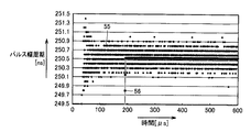
FIG. 8 is a diagram showing a measurement result of the output of the oscillation circuit when the
図8においても、図6、図7の場合と同様に、図の横軸はイネーブル信号EnableがHレベル(活性状態)になってからの経過時間であり、縦軸はクロック信号のパルス幅周期である。また、図中には、各時刻ごとのパルス幅周期の測定値55と、155.5μ秒の区間ごとに測定値55を移動平均した移動平均値56とが示されている。
In FIG. 8 as well, in the same manner as in FIGS. 6 and 7, the horizontal axis in the figure is the elapsed time after the enable signal Enable becomes H level (active state), and the vertical axis is the pulse width period of the clock signal. It is. In the figure, a measured
図6の場合と同様の方法によって起動時間を評価すると、図8の場合には到達時間は192.7μ秒と求められるので、起動時間は37.2μ秒と評価することができる。すなわち、CMOSインバータ換算で論理素子の段数が1段から5段に増加することによって起動時間が約1/6に短縮できることがわかる。 If the activation time is evaluated by the same method as in FIG. 6, the arrival time is obtained as 192.7 μsec in the case of FIG. 8, and thus the activation time can be evaluated as 37.2 μsec. That is, it can be seen that the startup time can be shortened to about 1/6 by increasing the number of logic elements from 1 to 5 in terms of a CMOS inverter.
以上のとおり、実施の形態1の発振回路1によれば、多段構成のCMOS論理素子を用いて圧電振動子XOの出力を反転増幅することによって、発振開始直後の圧電振動子XOの励振レベルRe×I2における交流電流Iの大きさを増加させることができる。この結果、圧電振動子XOの発振が安定するまでの起動時間を短縮することができる。 As described above, according to the oscillation circuit 1 of the first embodiment, the excitation level Re of the piezoelectric vibrator XO immediately after the start of oscillation is obtained by inverting and amplifying the output of the piezoelectric vibrator XO using a multistage CMOS logic element. The magnitude of the alternating current I at × I 2 can be increased. As a result, the startup time until the oscillation of the piezoelectric vibrator XO is stabilized can be shortened.
なお、図1の各インバータ回路L2,L3は、一方の入力がHレベルに固定されたNAND回路、または一方の入力がLレベルに固定されたNOR回路、または一方の入力がHレベルに固定されたXOR(排他的論理和)回路などに置換えることができる。 Each of the inverter circuits L2 and L3 in FIG. 1 has a NAND circuit in which one input is fixed at the H level, a NOR circuit in which one input is fixed at the L level, or one input is fixed at the H level. It can be replaced with an XOR (exclusive OR) circuit or the like.
また、図1のNAND回路L1は、NOR回路に置換えることもできる。NOR回路の場合は、イネーブル信号EnableはLレベルのとき活性状態である。 Further, the NAND circuit L1 in FIG. 1 can be replaced with a NOR circuit. In the case of a NOR circuit, the enable signal Enable is in an active state when it is at L level.
また、イネーブル信号Enableが入力されるNAND回路L1は、図1のように従属接続されたCMOS論理素子の初段に配置する必要はない。励振回路10を構成する論理素子の少なくとも1つにイネーブル信号Enableの入力用のNAND回路L1を配置すればよい。
Further, the NAND circuit L1 to which the enable signal Enable is input does not need to be arranged at the first stage of the cascade-connected CMOS logic elements as shown in FIG. The NAND circuit L1 for inputting the enable signal Enable may be disposed in at least one of the logic elements constituting the
実施の形態1をさらに一般化すると、励振回路10を構成する従属接続された複数の論理素子の各々は、インバータ、NAND回路、NOR回路、AND回路、OR回路、XOR回路、バッファ、3ステートバッファなどのいずれの論理素子であってもよい。ただし、励振回路10全体として入力信号の論理レベルを反転するように組合わせる必要がある。この場合、NAND回路、NOR回路、AND回路、OR回路、XOR回路など2入力の論理素子をインバータまたはバッファ(スルー回路)の代わりに用いる場合には、入力の一方をHレベルまたはLレベルに固定する。
To further generalize the first embodiment, each of a plurality of cascade-connected logic elements constituting the
さらに、上記の実施の形態1では、CMOS論理素子を例に挙げて説明したが、論理素子はCMOS型に限る必要はない。たとえば、CMOS論理素子に代えて、PチャネルMOSトランジスタのみを用いて論理素子を構成してもよいし、もしくは、NチャネルMOSトランジスタのみを用いて論理素子を構成してもよい。 Furthermore, in the first embodiment, the CMOS logic element is described as an example, but the logic element is not necessarily limited to the CMOS type. For example, instead of a CMOS logic element, a logic element may be configured using only a P-channel MOS transistor, or a logic element may be configured using only an N-channel MOS transistor.
[実施の形態2]
図9は、この発明の実施の形態2による発振回路2の構成を示す回路図である。図9の発振回路2は、ノードXIN,XOUT間で第1の励振回路10と並列に設けられた第2の励振回路20をさらに含む点で図1の発振回路1と異なる。
[Embodiment 2]
FIG. 9 is a circuit diagram showing a configuration of
第2の励振回路20は、ノードXINの信号を反転増幅してノードXOUTに出力する。この点で第1の励振回路10と同じであるが、CMOSインバータで換算したときに第1の励振回路10よりも少ない段数の従属接続された論理素子で構成される点で第1の励振回路10と異なる。この結果、第2の励振回路20の電力増幅率は第1の励振回路10よりも小さく、圧電振動子XOの励振レベルRe×I2における交流電流Iの大きさも小さい。
The
具体的に図9の場合、第2の励振回路20は、ノードXIN,XOUT間に接続された2入力のNAND回路L4を含む。NAND回路L4の一方の入力端子にはイネーブル信号Enableが入力され、NAND回路L4の他方の入力端子は入力ノードXINと接続される。イネーブル信号EnableがLレベル(非活性状態)の間は、NAND回路L4の出力はHレベルに固定され、イネーブル信号EnableがHレベル(活性状態)になると、NAND回路L4は圧電振動子XOを励振するためのインバータとして動作する。
Specifically, in the case of FIG. 9, the
図9の発振回路2は、さらに、タイマー回路30と、ノードXINと第1の励振回路10の入力端(NAND回路L1の一方の入力端子)との間に設けられたスイッチSW1と、ノードXOUTと第1の励振回路10の出力端(インバータL3の出力端子)との間に設けられたスイッチSW2とを含む。
9 further includes a
タイマー回路30は、イネーブル信号EnableがHレベル(活性状態)になったときから予め定める時間だけ活性状態になる制御信号CTLを出力する。タイマー回路は、イネーブル信号EnableのタイミングをずらすためにCR積分回路などの遅延回路を用いて構成することができる。あるいは、別のクロック信号を利用したカウンタ回路を用いてもタイマー回路を構成することができる。
The
スイッチSW1,SW2は制御信号CTLを受け、制御信号CTLが活性状態のときに導通し、制御信号CTLが非活性状態になると非導通状態になる。スイッチSW1,SW2が導通することによって、圧電振動子XOは、並列接続された第1および第2の励振回路10,20の両方で励振されることになる。また、スイッチSW1,SW2が非導通状態になると、圧電振動子XOは第2の励振回路20のみで励振されることになる。
The switches SW1 and SW2 receive the control signal CTL and are turned on when the control signal CTL is in an active state, and are turned off when the control signal CTL is in an inactive state. When the switches SW1 and SW2 are turned on, the piezoelectric vibrator XO is excited by both the first and
したがって、実施の形態2の発振回路2によれば、制御信号CTLが活性状態である発振起動時には並列接続された第1の励振回路10および第2の励振回路20を用いることによって起動時間を短縮させることができる。そして、制御信号CTLが非活性状態に戻った発振安定後には第1の励振回路10よりも電力増幅率の小さな第2の励振回路20のみを用いることによって、発振回路2全体の消費電力を低減させることができる。
Therefore, according to the
[実施の形態3]
実施の形態3の発振回路3は、実施の形態2の発振回路2のスイッチSW1,SW2に代えて、3ステートバッファを用いたものである。3ステートバッファは、スイッチSW1,SW2としての役割とともに、圧電振動子XOの励振加速用に用いられる第1の励振回路の論理素子の役割も兼ねる。なお、以下の説明では、実施の形態1,2と異なる点について主に説明し、同一または相当する部分については同一の参照符号を付して説明を繰返さない場合がある。
[Embodiment 3]
The
図10は、この発明の実施の形態3による発振回路3の構成を示す回路図である。図10を参照して、発振回路3は、入力ノードXINと出力ノードとの間に互いに並列に接続された圧電振動子XO、抵抗素子R1、第1の励振回路12、および第2の励振回路20と、ノードXINと接地ノードGNDとの間に接続されたコンデンサ(容量素子)C1と、ノードXOUTと接地ノードGNDとの間に接続されたコンデンサ(容量素子)C2と、タイマー回路30Aと、出力ノードXOUTの信号を整形するためのインバータL9とを含む。
FIG. 10 is a circuit diagram showing a configuration of
第1の励振回路12は、発振起動時にノードXINの信号を反転増幅してノードXOUTに出力するための回路であり、3ステートバッファL5,L6とNAND回路L1とを含む。3ステートバッファL5、NAND回路L1、および3ステートバッファL6は、この順でノードXIN,XOUT間に直列に接続される。第1の励振回路12は、さらに、3ステートバッファL5およびNAND回路L1を接続する接続ノードEと接地ノードGNDとの間に設けられた抵抗素子R3を含む。抵抗素子R3は、3ステートバッファの出力がハイ・インピーダンスのときに接続ノードEの電圧を接地電圧に固定するためのプルダウン抵抗として設けられている。
The
NAND回路L1の一方の入力端子は、後述するタイマー回路30AのノードDに接続される。したがって、NAND回路L1は、ノードDの電圧がHレベル(活性状態)のときインバータとして動作し、ノードDの電圧がLレベル(非活性状態)のとき出力がHレベルに固定される。
One input terminal of the NAND circuit L1 is connected to a node D of a
3ステートバッファL5、L6は、ゲート端子に入力された信号がLレベルのとき入力信号をそのまま出力し、ゲート端子に入力された信号がHレベルのとき出力をハイ・インピーダンスにする。ゲート端子にはノードDの信号の論理レベルを反転させた信号が入力される。したがって、3ステートバッファL5、L6は、ノードDの電圧がHレベル(活性状態)のときバッファとして動作し、ノードDの電圧がLレベル(非活性状態)のとき出力をハイ・インピーダンスに固定する。 The three-state buffers L5 and L6 output the input signal as it is when the signal input to the gate terminal is at L level, and set the output to high impedance when the signal input to the gate terminal is at H level. A signal obtained by inverting the logic level of the signal at the node D is input to the gate terminal. Therefore, the three-state buffers L5 and L6 operate as buffers when the voltage at the node D is at the H level (active state), and fix the output to high impedance when the voltage at the node D is at the L level (inactive state). .
第2の励振回路20は、ノードXINの信号を反転増幅してノードXOUTに出力するための回路であり、ノードXIN,XOUT間に接続されたNAND回路L4を含む。NAND回路L4の一方の入力端子はイネーブル信号Enableが入力されるイネーブル端子8と接続され、NAND回路L4の他方の入力端子は入力ノードXINと接続される。したがって、イネーブル信号EnableがLレベル(非活性状態)の間は、NAND回路L4の出力はHレベルに固定され、イネーブル信号EnableがHレベル(活性状態)になると、NAND回路L4は圧電振動子XOを励振するためのインバータとして動作する。
The
タイマー回路30Aは、イネーブル信号EnableがHレベル(活性状態)になったときから予め定める時間だけノードDの電圧をHレベル(活性状態)にする。タイマー回路30Aは、インバータL11,L12,L13と、3ステートバッファL14と、抵抗素子R2,R4と、コンデンサ(容量素子)C3とを含む。抵抗素子R2、インバータL11、および3ステートバッファL14は、この順でイネーブル信号Enableが入力されるイネーブル端子8とノードDとの間に直列に接続される。
The
コンデンサC3は、抵抗素子R2とインバータL11とを接続する接続ノードAと、接地ノードGNDとの間に接続される。コンデンサC3と抵抗素子R2とによってCR積分回路が構成される。 Capacitor C3 is connected between connection node A connecting resistance element R2 and inverter L11, and ground node GND. The CR integration circuit is configured by the capacitor C3 and the resistance element R2.
インバータL12は、イネーブル端子8と3ステートバッファL14のゲート端子との間に接続される。したがって、3ステートバッファL14は、イネーブル信号EnableがHレベル(活性状態)のときバッファとして動作する。 Inverter L12 is connected between enable terminal 8 and the gate terminal of 3-state buffer L14. Therefore, the 3-state buffer L14 operates as a buffer when the enable signal Enable is at the H level (active state).
インバータL13の入力端子はノードDに接続され、インバータL13の出力端子(ノード/D)は3ステートバッファL5,L6の各ゲート端子に接続される。抵抗素子R4は、ノードDと接地ノードGNDとの間に固定され、3ステートバッファL14の出力がハイ・インピーダンスのとき、ノードDの電圧をLレベルに固定するためのプルダウン抵抗として用いられる。 The input terminal of inverter L13 is connected to node D, and the output terminal (node / D) of inverter L13 is connected to the gate terminals of tristate buffers L5 and L6. Resistor element R4 is fixed between node D and ground node GND, and is used as a pull-down resistor for fixing the voltage at node D to L level when the output of 3-state buffer L14 is high impedance.
次に、発振回路3の動作について説明する。
図11は、図10の発振回路3の各部における電圧波形を模式的に示した図である。図11には、上から順に、イネーブル信号Enableの電圧波形と、図10のノードA,B,C,D,/D,E,Fの各電圧波形とが示される。
Next, the operation of the
FIG. 11 is a diagram schematically showing voltage waveforms in each part of the
図10、図11を参照して、時刻t1でイネーブル信号EnableがLレベル(非活性状態)からHレベル(活性状態)に変化すると、コンデンサC3の充電に伴なってコンデンサC3と抵抗素子R2との接続ノードAの電圧は徐々に上昇する。この結果、インバータL11の出力端子(ノードB)の電圧は、ノードAの電圧がインバータL11の閾値電圧を超える時刻t2までHレベルとなり、時刻t2以降Lレベルになる。 10 and 11, when enable signal Enable changes from L level (inactive state) to H level (active state) at time t1, capacitor C3 and resistance element R2 The voltage at the connection node A gradually increases. As a result, the voltage at the output terminal (node B) of inverter L11 becomes H level until time t2 when the voltage at node A exceeds the threshold voltage of inverter L11, and becomes L level after time t2.
インバータL12の出力端子(ノードC)の電圧は、イネーブル信号Enableを反転させたものである。3ステートバッファL14のゲート端子にはノードCの電圧が入力されるので、時刻t1以降、イネーブル信号EnableがLレベルに戻る時刻t3までの間、3ステートバッファL14はバッファ回路として動作する。この結果、3ステートバッファL14の出力端子(ノードD)の電圧は、時刻t1〜t3の間はノードBの電圧と同様に変化する。すなわち、時刻t1〜t2の間、ノードDの電圧はHレベルになり、時刻t1以前および時刻t2以降はLレベルになる。また、インバータL13の出力端子(ノード/D)の電圧はノードDと逆であり、時刻t1〜t2の間がLレベルであり、時刻t1以前および時刻t2以降はHレベルになる。 The voltage at the output terminal (node C) of the inverter L12 is obtained by inverting the enable signal Enable. Since the voltage of the node C is input to the gate terminal of the 3-state buffer L14, the 3-state buffer L14 operates as a buffer circuit from time t1 until time t3 when the enable signal Enable returns to L level. As a result, the voltage at the output terminal (node D) of the three-state buffer L14 changes in the same manner as the voltage at node B between times t1 and t3. That is, the voltage of the node D is at the H level between the times t1 and t2, and is at the L level before the time t1 and after the time t2. The voltage at the output terminal (node / D) of inverter L13 is opposite to that of node D, and is at the L level between times t1 and t2, and is at the H level before time t1 and after time t2.
3ステートバッファL5,L6の各ゲート電極はノード/Dに接続される。したがって、ノード/Dの電圧がLレベル(ノードDの電圧がHレベル)となる時刻t1〜t2の間、3ステートバッファL5,L6はバッファ回路として動作する。時刻t1以前および時刻t2以降については、3ステートバッファL5の出力端子(ノードE)はLレベルに固定されるので、NAND回路L1の出力端子(ノードF)はHレベルに固定される。したがって、時刻t1〜t2の間、ノードE,Fの電圧は圧電振動子XOの発振に伴なって振動する。 Each gate electrode of 3-state buffers L5 and L6 is connected to node / D. Therefore, the three-state buffers L5 and L6 operate as a buffer circuit between times t1 and t2 when the voltage of the node / D becomes L level (the voltage of the node D is H level). Before time t1 and after time t2, the output terminal (node E) of the 3-state buffer L5 is fixed at the L level, so the output terminal (node F) of the NAND circuit L1 is fixed at the H level. Therefore, between times t1 and t2, the voltages at the nodes E and F vibrate with the oscillation of the piezoelectric vibrator XO.
このように、イネーブル信号EnableがHレベル(活性状態)になった時刻t1から開始して時刻t2までの間、第1の励振回路12によって圧電振動子XOは励振される。時刻t2以降、第1の励振回路12による圧電振動子XOの励振は停止する。この時刻t1〜t2の時間は、抵抗素子R2の抵抗値およびコンデンサC3の容量値によって決まる積分回路の時定数に依存する。
Thus, the piezoelectric vibrator XO is excited by the
一方、第2の励振回路20を構成するNAND回路L4は、イネーブル信号EnableがHレベル(活性状態)である時刻t1〜t3の間、圧電振動子XOを励振する。したがって、時刻t1〜t2の発振起動時には第1および第2の励振回路12,20がともに動作するのに対して、時刻t2〜t3の発振安定時には第2の励振回路20のみが動作する。これによって、発振安定時の消費電力を低減することができる。
On the other hand, the NAND circuit L4 constituting the
以下、図10の発振回路3の各部の電圧波形を測定した実験結果について説明する。実験では、図10の圧電振動子XOとしてセラミック振動子を用い、抵抗素子R1の抵抗値を1MΩに設定した。まず、図10のイネーブル信号、ノードDの電圧、ノードEの電圧、およびクロック信号CLKをオシロスコープで測定した結果について説明する。
Hereinafter, experimental results obtained by measuring voltage waveforms at various parts of the
図12は、図10の発振回路3の各部における電圧変化を測定した波形図である。図の縦軸は電圧を示し、横軸は時間を示す。画面上の格子状の1目盛(ディビジョン)あたり、横軸は20μ秒を表わす。また、縦軸の1目盛(ディビジョン)あたり、イネーブル信号Enableは1Vを表わし、ノードD,Eの電圧およびクロック信号CLKは2Vを表わす。
FIG. 12 is a waveform diagram obtained by measuring a voltage change in each part of the
図12に示すように、イネーブル信号EnableがHレベルに立上がると、ノードDの電圧もHレベルに立上がる。そして、ノードDの電圧は、イネーブル信号Enableが立ち上がってから約30μ秒が経過したときに立ち下がる。既に説明したように、ノードDの電圧がHレベルである時間(30μ秒)は、図10の抵抗素子R2の抵抗値およびコンデンサC3の容量値に依存して調整可能である。 As shown in FIG. 12, when enable signal Enable rises to H level, the voltage at node D also rises to H level. Then, the voltage at the node D falls when about 30 μsec elapses after the enable signal Enable rises. As already described, the time during which the voltage at the node D is at the H level (30 μs) can be adjusted depending on the resistance value of the resistance element R2 and the capacitance value of the capacitor C3 in FIG.
ノードEの電圧は、ノードDの電圧がHレベル(活性状態)の間、発振した圧電振動子XOの電圧を受けて振動する。また、クロック信号CLKは、イネーブル信号EnableがHレベル(活性状態)の間に出力される。 The voltage of the node E vibrates in response to the voltage of the oscillating piezoelectric vibrator XO while the voltage of the node D is at the H level (active state). The clock signal CLK is output while the enable signal Enable is at the H level (active state).
次に、クロック信号CLKをタイムインターバルアナライザ(YOKOGAWA TA320)でモニターし、クロック信号CLKのパルス幅周期を測定した結果について説明する。 Next, the result of monitoring the clock signal CLK with a time interval analyzer (YOKOGAWA TA320) and measuring the pulse width period of the clock signal CLK will be described.
図13は、図10の発振回路3の起動時間を測定した実験結果を示す図である。図13(B)は図13(A)の拡大図である。図13(A),(B)の横軸はイネーブル信号EnableがHレベル(活性状態)になってからの経過時間であり、縦軸はクロック信号のパルス幅周期である。図中には、各時刻ごとのパルス幅周期の測定値57と、155.5μ秒の区間ごとに測定値57を移動平均した移動平均値58とが示されている。
FIG. 13 is a diagram showing experimental results obtained by measuring the startup time of the
図6〜図8の場合と同様に起動時間を評価すると、図7の場合の到達時間は184.0μ秒と求められるので、起動時間は28.5μ秒と評価できる。この起動時間は、図6〜図8のいずれの場合よりも短くなっている。この理由は、3ステートバッファL5,L6がバッファ回路として動作するときは4段のインバータ回路と等価であるので、図6〜図8のいずれの場合よりも実施の形態3の発振回路3のほうがCMOSインバータ換算での論理素子の段数が多くなっているからである。
When the activation time is evaluated in the same manner as in FIGS. 6 to 8, the arrival time in the case of FIG. 7 is determined to be 184.0 μsec. This activation time is shorter than in any case of FIGS. This is because the three-state buffers L5 and L6 are equivalent to a four-stage inverter circuit when operating as a buffer circuit, and therefore the
このように、実施の形態3の発振回路3によれば、第1の励振回路12を構成する論理素子のうち初段および最終段の論理素子を3ステートバッファで構成することによって、実施の形態2の発振回路2のスイッチSW1,SW2に代用することができる。この結果、実施の形態2の発振回路2と同様に、発振起動時には並列接続された第1の励振回路12および第2の励振回路20を用いることによって起動時間を短縮させることができる。そして、発振安定後には第1の励振回路12よりも電力増幅率の小さな第2の励振回路20のみを用いることによって、発振回路2全体の消費電力を低減させることができる。
As described above, according to the
[実施の形態4]
図14は、この発明の実施の形態4による発振回路4の構成を示す回路図である。図14の発振回路4は、信号の経路を開閉する開閉スイッチSW1,SW2に代えて、信号の経路を切換える切換スイッチSW3,SW4を含む点で、図9の発振回路2と異なる。その他の点については、発振回路4は実施の形態2の発振回路2と共通するので、同一または相当する部分には同一の参照符号を付して説明を繰り返さない。
[Embodiment 4]
FIG. 14 is a circuit diagram showing a configuration of oscillation circuit 4 according to the fourth embodiment of the present invention. The oscillation circuit 4 of FIG. 14 differs from the
切換スイッチSW3は、タイマー回路30から出力された制御信号CTLを受け、制御信号CTLが活性状態のときにノードXINと第1の励振回路10の入力端(NAND回路L1の一方の入力端子)とを接続する。さらに、切換スイッチSW3は、制御信号CTLが非活性状態のときにノードXINと第2の励振回路20の入力端(NAND回路L4の一方の入力端子)とを接続する。
The change-over switch SW3 receives the control signal CTL output from the
切換スイッチSW4は、タイマー回路30から出力された制御信号CTLを受け、制御信号CTLが活性状態のときにノードXINと第1の励振回路10の出力端(インバータL3の出力端子)とを接続する。さらに、切換スイッチSW4は、制御信号CTLが非活性状態のときにノードXINと第2の励振回路20の出力端(NAND回路L4の出力端子)とを接続する。
The changeover switch SW4 receives the control signal CTL output from the
これによって、発振起動時には、第2の励振回路20よりも電力増幅率の大きな第1の励振回路10のみを用いることによって起動時間を短縮させることができる。そして、発振安定後には、第1の励振回路10よりも電力増幅率の小さな第2の励振回路20のみを用いることによって、発振回路2全体の消費電力を低減させることができる。
Thus, at the time of oscillation start-up, the start-up time can be shortened by using only the
今回開示された実施の形態はすべての点で例示であって制限的なものでないと考えられるべきである。この発明の範囲は上記した説明ではなくて請求の範囲によって示され、請求の範囲と均等の意味および範囲内でのすべての変更が含まれることが意図される。 The embodiment disclosed this time must be considered as illustrative in all points and not restrictive. The scope of the present invention is defined by the terms of the claims, rather than the description above, and is intended to include any modifications within the scope and meaning equivalent to the terms of the claims.
1〜4,101 発振回路、10,12 第1の励振回路、20 第2の励振回路、30,30A タイマー回路、C1,C2 コンデンサ、CLK クロック信号、CTL 制御信号、Enable イネーブル信号、GND 接地ノード、L1,L4 NAND回路、L2,L3,L9 インバータ、L11,L12,L13 インバータ、L5,L6,L14 3ステートバッファ、R1〜R4 抵抗素子、SW1,SW2 開閉スイッチ、SW3,SW4 切換スイッチ、VDD 電源ノード、XIN 入力ノード(第1のノード)、XO 圧電振動子、XOUT 出力ノード(第2のノード)。 1-4, 101 Oscillator circuit, 10, 12 First excitation circuit, 20 Second excitation circuit, 30, 30A Timer circuit, C1, C2 capacitor, CLK clock signal, CTL control signal, Enable enable signal, GND Ground node , L1, L4 NAND circuit, L2, L3, L9 inverter, L11, L12, L13 inverter, L5, L6, L14 3-state buffer, R1-R4 resistance element, SW1, SW2 open / close switch, SW3, SW4 selector switch, VDD power supply Node, XIN input node (first node), XO piezoelectric vibrator, XOUT output node (second node).
Claims (5)
前記第1および第2のノード間に前記圧電振動子と並列に設けられた抵抗素子と、
前記第1のノードと接地ノードとの間に設けられた第1の容量素子と、
前記第2のノードと接地ノードとの間に設けられた第2の容量素子と、
前記第1および第2のノード間に前記圧電振動子および前記抵抗素子の各々と並列に設けられ、前記第1のノードの信号を反転増幅して第2のノードに出力するための第1の励振回路とを備え、
前記第1の励振回路は、各々が増幅回路として用いられる従属接続された複数の論理素子を含む、発振回路。 A piezoelectric vibrator provided between the first and second nodes;
A resistance element provided in parallel with the piezoelectric vibrator between the first and second nodes;
A first capacitive element provided between the first node and a ground node;
A second capacitive element provided between the second node and a ground node;
A first node is provided between the first node and the second node in parallel with each of the piezoelectric vibrator and the resistance element, and inverts and amplifies the signal of the first node and outputs the signal to the second node. An excitation circuit,
The first excitation circuit is an oscillation circuit including a plurality of cascade-connected logic elements each used as an amplifier circuit.
イネーブル信号が活性状態になったときから予め定める時間だけ活性状態になる制御信号を出力するタイマー回路と、
前記第1および第2のノード間に前記圧電振動子、前記抵抗素子、および前記第1の励振回路の各々と並列に設けられ、前記第1のノードの信号を反転増幅して前記第2のノードに出力するための第2の励振回路とをさらに備え、
前記第2の励振回路の電力増幅率は、前記第1の励振回路の電力増幅率より小さく、
前記第2の励振回路は、前記イネーブル信号が非活性状態のとき一定の論理レベルの信号を出力し、前記イネーブル信号が活性状態のとき増幅回路として動作する論理素子を含み、
前記第1の励振回路を構成する複数の論理素子のうち初段および最終段の論理素子は、前記制御信号が非活性状態のとき高インピーダンス状態になる3ステートバッファである、請求項1に記載の発振回路。 The oscillation circuit is
A timer circuit that outputs a control signal that becomes active only for a predetermined time from when the enable signal becomes active;
Provided in parallel with each of the piezoelectric vibrator, the resistance element, and the first excitation circuit between the first and second nodes, inverting and amplifying the signal of the first node, and A second excitation circuit for outputting to the node,
The power amplification factor of the second excitation circuit is smaller than the power amplification factor of the first excitation circuit,
The second excitation circuit includes a logic element that outputs a signal of a constant logic level when the enable signal is in an inactive state and operates as an amplifier circuit when the enable signal is in an active state;
The first-stage and last-stage logic elements among the plurality of logic elements constituting the first excitation circuit are three-state buffers that are in a high impedance state when the control signal is in an inactive state. Oscillator circuit.
イネーブル信号が活性状態になったときから予め定める時間だけ活性状態になる制御信号を出力するタイマー回路と、
前記第1のノードと前記第1の励振回路の入力端との間に設けられ、前記制御信号が活性状態のときオン状態になり、前記制御信号が非活性状態のときオフ状態になる第1のスイッチと、
前記第2のノードと前記第1の励振回路の出力端との間に設けられ、前記制御信号が活性状態のときオン状態になり、前記制御信号が非活性状態のときオフ状態になる第2のスイッチと、
前記第1および第2のノード間に前記圧電振動子、前記抵抗素子、および前記第1の励振回路の各々と並列に設けられ、前記第1のノードの信号を反転増幅して前記第2のノードに出力するための第2の励振回路とをさらに備え、
前記第2の励振回路の電力増幅率は、前記第1の励振回路の電力増幅率より小さく、
前記第2の励振回路は、前記イネーブル信号が非活性状態のとき一定の論理レベルの信号を出力し、前記イネーブル信号が活性状態のとき増幅回路として動作する論理素子を含む、請求項1に記載の発振回路。 The oscillation circuit is
A timer circuit that outputs a control signal that becomes active only for a predetermined time from when the enable signal becomes active;
A first node is provided between the first node and the input end of the first excitation circuit, and is turned on when the control signal is in an active state and turned off when the control signal is in an inactive state. And the switch
A second node is provided between the second node and the output terminal of the first excitation circuit, and is turned on when the control signal is in an active state and turned off when the control signal is in an inactive state. And the switch
Provided in parallel with each of the piezoelectric vibrator, the resistance element, and the first excitation circuit between the first and second nodes, inverting and amplifying the signal of the first node, and A second excitation circuit for outputting to the node,
The power amplification factor of the second excitation circuit is smaller than the power amplification factor of the first excitation circuit,
The second excitation circuit includes a logic element that outputs a signal having a constant logic level when the enable signal is in an inactive state and operates as an amplifier circuit when the enable signal is in an active state. Oscillation circuit.
前記第2の励振回路の電力増幅率は、前記第1の励振回路の電力増幅率より小さく、
前記発振回路は、
イネーブル信号が活性状態になったときから予め定める時間だけ活性状態になる制御信号を出力するタイマー回路と、
前記制御信号が活性状態のときに前記第1の励振回路の入力端と前記第1のノードとを接続し、前記イネーブル信号が活性状態であり、かつ、前記制御信号が非活性状態であるときに前記第2の励振回路の入力端と前記第1のノードとを接続する第1のスイッチと、
前記制御信号が活性状態のときに前記第1の励振回路の出力端と前記第2のノードとを接続し、前記イネーブル信号が活性状態であり、かつ、前記制御信号が非活性状態であるときに前記第2の励振回路の出力端と前記第2のノードとを接続する第2のスイッチとをさらに備える、請求項1に記載の発振回路。 The oscillation circuit is provided between the first and second nodes in parallel with each of the piezoelectric vibrator, the resistance element, and the first excitation circuit, and inverts and amplifies the signal of the first node. And a second excitation circuit for outputting to the second node.
The power amplification factor of the second excitation circuit is smaller than the power amplification factor of the first excitation circuit,
The oscillation circuit is
A timer circuit that outputs a control signal that becomes active only for a predetermined time from when the enable signal becomes active;
When the control signal is in an active state, the input terminal of the first excitation circuit is connected to the first node, the enable signal is in an active state, and the control signal is in an inactive state A first switch for connecting the input terminal of the second excitation circuit to the first node;
When the output signal of the first excitation circuit and the second node are connected when the control signal is in an active state, the enable signal is in an active state, and the control signal is in an inactive state The oscillation circuit according to claim 1, further comprising: a second switch that connects an output terminal of the second excitation circuit and the second node.
Priority Applications (5)
| Application Number | Priority Date | Filing Date | Title |
|---|---|---|---|
| JP2009013388A JP2010171810A (en) | 2009-01-23 | 2009-01-23 | Oscillation circuit |
| EP10733445.0A EP2242175B1 (en) | 2009-01-23 | 2010-01-18 | Oscillator circuit |
| US12/865,525 US8232847B2 (en) | 2009-01-23 | 2010-01-18 | Oscillation circuit |
| CN2010800010588A CN101933223A (en) | 2009-01-23 | 2010-01-18 | Oscillator circuit |
| PCT/JP2010/050488 WO2010084838A1 (en) | 2009-01-23 | 2010-01-18 | Oscillator circuit |
Applications Claiming Priority (1)
| Application Number | Priority Date | Filing Date | Title |
|---|---|---|---|
| JP2009013388A JP2010171810A (en) | 2009-01-23 | 2009-01-23 | Oscillation circuit |
Publications (1)
| Publication Number | Publication Date |
|---|---|
| JP2010171810A true JP2010171810A (en) | 2010-08-05 |
Family
ID=42355892
Family Applications (1)
| Application Number | Title | Priority Date | Filing Date |
|---|---|---|---|
| JP2009013388A Pending JP2010171810A (en) | 2009-01-23 | 2009-01-23 | Oscillation circuit |
Country Status (5)
| Country | Link |
|---|---|
| US (1) | US8232847B2 (en) |
| EP (1) | EP2242175B1 (en) |
| JP (1) | JP2010171810A (en) |
| CN (1) | CN101933223A (en) |
| WO (1) | WO2010084838A1 (en) |
Cited By (2)
| Publication number | Priority date | Publication date | Assignee | Title |
|---|---|---|---|---|
| JP2018042012A (en) * | 2016-09-05 | 2018-03-15 | ローム株式会社 | Semiconductor integrated circuit |
| JP2018198420A (en) * | 2017-04-18 | 2018-12-13 | スティヒティング・イメック・ネーデルラントStichting IMEC Nederland | Quartz crystal circuit and activation method of crystal unit |
Families Citing this family (3)
| Publication number | Priority date | Publication date | Assignee | Title |
|---|---|---|---|---|
| DE102009011840B4 (en) | 2009-03-05 | 2020-07-02 | Intel Deutschland Gmbh | Oscillator circuit with fast settling process |
| CN101977057B (en) * | 2010-11-04 | 2013-05-22 | 青岛海信移动通信技术股份有限公司 | An analog-to-digital conversion circuit |
| US8975972B2 (en) * | 2012-07-05 | 2015-03-10 | Infineon Technologies Ag | Oscillator system |
Citations (6)
| Publication number | Priority date | Publication date | Assignee | Title |
|---|---|---|---|---|
| JPS6292522A (en) * | 1985-10-18 | 1987-04-28 | Hitachi Ltd | Analog voltage output circuit |
| JPS62109406A (en) * | 1985-11-07 | 1987-05-20 | Nec Corp | Oscillation circuit |
| JPH09289416A (en) * | 1996-04-23 | 1997-11-04 | Nec Shizuoka Ltd | Crystal oscillation circuit |
| JP2000031740A (en) * | 1998-07-08 | 2000-01-28 | Hitachi Ltd | Oscillator circuit |
| JP2002135052A (en) * | 2000-10-20 | 2002-05-10 | Matsushita Electric Ind Co Ltd | Crystal oscillator and method for controlling the same |
| JP2005079648A (en) * | 2003-08-28 | 2005-03-24 | Seiko Epson Corp | Oscillation circuit and semiconductor integrated circuit |
Family Cites Families (6)
| Publication number | Priority date | Publication date | Assignee | Title |
|---|---|---|---|---|
| JPS5991709A (en) | 1982-11-18 | 1984-05-26 | Matsushita Electric Ind Co Ltd | Crystal oscillating circuit |
| US5208558A (en) * | 1990-11-29 | 1993-05-04 | Kabushiki Kaisha Toshiba | Crystal oscillator having plural inverters disabled after start-up |
| JP3288830B2 (en) * | 1993-10-28 | 2002-06-04 | 日本プレシジョン・サーキッツ株式会社 | Oscillation integrated circuit |
| JPH11234043A (en) * | 1998-02-19 | 1999-08-27 | Toshiba Corp | Oscillation circuit and semiconductor integrated circuit |
| JP2001016099A (en) | 1999-07-01 | 2001-01-19 | Nec Ic Microcomput Syst Ltd | Digital pll circuit and control method therefor |
| JP2008147815A (en) * | 2006-12-07 | 2008-06-26 | Sanyo Electric Co Ltd | Oscillation circuit |
-
2009
- 2009-01-23 JP JP2009013388A patent/JP2010171810A/en active Pending
-
2010
- 2010-01-18 WO PCT/JP2010/050488 patent/WO2010084838A1/en active Application Filing
- 2010-01-18 US US12/865,525 patent/US8232847B2/en not_active Expired - Fee Related
- 2010-01-18 CN CN2010800010588A patent/CN101933223A/en active Pending
- 2010-01-18 EP EP10733445.0A patent/EP2242175B1/en active Active
Patent Citations (6)
| Publication number | Priority date | Publication date | Assignee | Title |
|---|---|---|---|---|
| JPS6292522A (en) * | 1985-10-18 | 1987-04-28 | Hitachi Ltd | Analog voltage output circuit |
| JPS62109406A (en) * | 1985-11-07 | 1987-05-20 | Nec Corp | Oscillation circuit |
| JPH09289416A (en) * | 1996-04-23 | 1997-11-04 | Nec Shizuoka Ltd | Crystal oscillation circuit |
| JP2000031740A (en) * | 1998-07-08 | 2000-01-28 | Hitachi Ltd | Oscillator circuit |
| JP2002135052A (en) * | 2000-10-20 | 2002-05-10 | Matsushita Electric Ind Co Ltd | Crystal oscillator and method for controlling the same |
| JP2005079648A (en) * | 2003-08-28 | 2005-03-24 | Seiko Epson Corp | Oscillation circuit and semiconductor integrated circuit |
Cited By (3)
| Publication number | Priority date | Publication date | Assignee | Title |
|---|---|---|---|---|
| JP2018042012A (en) * | 2016-09-05 | 2018-03-15 | ローム株式会社 | Semiconductor integrated circuit |
| JP2018198420A (en) * | 2017-04-18 | 2018-12-13 | スティヒティング・イメック・ネーデルラントStichting IMEC Nederland | Quartz crystal circuit and activation method of crystal unit |
| JP7307530B2 (en) | 2017-04-18 | 2023-07-12 | スティヒティング・イメック・ネーデルラント | Crystal oscillator circuit and crystal oscillator start-up method |
Also Published As
| Publication number | Publication date |
|---|---|
| US20110001570A1 (en) | 2011-01-06 |
| WO2010084838A1 (en) | 2010-07-29 |
| EP2242175A1 (en) | 2010-10-20 |
| EP2242175B1 (en) | 2019-03-13 |
| CN101933223A (en) | 2010-12-29 |
| US8232847B2 (en) | 2012-07-31 |
| EP2242175A4 (en) | 2015-04-22 |
Similar Documents
| Publication | Publication Date | Title |
|---|---|---|
| US4321562A (en) | Crystal oscillator circuit capable of changing the number of inverter stages coupled in series | |
| US7250822B2 (en) | Clock oscillator | |
| JP2002204128A (en) | Oscillation circuit and integrated circuit for oscillation | |
| JPH1117451A (en) | Oscillation circuit | |
| WO2010084838A1 (en) | Oscillator circuit | |
| US5545941A (en) | Crystal oscillator circuit | |
| JP2002344242A (en) | Voltage-controlled oscillator | |
| CN105391419B (en) | Quartz oscillation circuit and electronic timepiece | |
| JP5048355B2 (en) | Oscillator circuit | |
| KR20080080447A (en) | Voltage control circuit | |
| JP3434774B2 (en) | Crystal oscillator | |
| JP4455734B2 (en) | Oscillator circuit | |
| JP2013214960A (en) | Crystal oscillation circuit and method of controlling crystal oscillation circuit | |
| US6690245B2 (en) | Oscillation control circuit | |
| JPH0575343A (en) | Clock signal output circuit | |
| JP2008099247A (en) | Transmitter ic with saw-based oscillator | |
| JP2006295362A (en) | Applied voltage control circuit for voltage controlled oscillator circuit | |
| JPH06232703A (en) | Oscillator | |
| US20240333214A1 (en) | Oscillation circuit and semiconductor integrated circuit | |
| JP2003283248A (en) | Semiconductor integrated circuit | |
| JPH066135A (en) | Crystal oscillator | |
| JP6522956B2 (en) | Clock generator, clock generation module, and clock source selection method | |
| JPH04273602A (en) | Oscillation control circuit | |
| JP5533052B2 (en) | Oscillator with signal generator | |
| JP2000269742A (en) | Inverter for oscillation and amplification, oscillation circuit, and frequency divider |
Legal Events
| Date | Code | Title | Description |
|---|---|---|---|
| A621 | Written request for application examination |
Free format text: JAPANESE INTERMEDIATE CODE: A621 Effective date: 20120110 |
|
| A131 | Notification of reasons for refusal |
Free format text: JAPANESE INTERMEDIATE CODE: A131 Effective date: 20121204 |
|
| A02 | Decision of refusal |
Free format text: JAPANESE INTERMEDIATE CODE: A02 Effective date: 20130402 |