JP2010098097A - Method for manufacturing molded package - Google Patents
Method for manufacturing molded package Download PDFInfo
- Publication number
- JP2010098097A JP2010098097A JP2008267232A JP2008267232A JP2010098097A JP 2010098097 A JP2010098097 A JP 2010098097A JP 2008267232 A JP2008267232 A JP 2008267232A JP 2008267232 A JP2008267232 A JP 2008267232A JP 2010098097 A JP2010098097 A JP 2010098097A
- Authority
- JP
- Japan
- Prior art keywords
- mold
- connector
- connector housing
- hole
- pin
- Prior art date
- Legal status (The legal status is an assumption and is not a legal conclusion. Google has not performed a legal analysis and makes no representation as to the accuracy of the status listed.)
- Granted
Links
Images


Classifications
-
- H—ELECTRICITY
- H01—ELECTRIC ELEMENTS
- H01L—SEMICONDUCTOR DEVICES NOT COVERED BY CLASS H10
- H01L2224/00—Indexing scheme for arrangements for connecting or disconnecting semiconductor or solid-state bodies and methods related thereto as covered by H01L24/00
- H01L2224/01—Means for bonding being attached to, or being formed on, the surface to be connected, e.g. chip-to-package, die-attach, "first-level" interconnects; Manufacturing methods related thereto
- H01L2224/42—Wire connectors; Manufacturing methods related thereto
- H01L2224/47—Structure, shape, material or disposition of the wire connectors after the connecting process
- H01L2224/48—Structure, shape, material or disposition of the wire connectors after the connecting process of an individual wire connector
- H01L2224/4805—Shape
- H01L2224/4809—Loop shape
- H01L2224/48091—Arched
-
- H—ELECTRICITY
- H01—ELECTRIC ELEMENTS
- H01L—SEMICONDUCTOR DEVICES NOT COVERED BY CLASS H10
- H01L2224/00—Indexing scheme for arrangements for connecting or disconnecting semiconductor or solid-state bodies and methods related thereto as covered by H01L24/00
- H01L2224/01—Means for bonding being attached to, or being formed on, the surface to be connected, e.g. chip-to-package, die-attach, "first-level" interconnects; Manufacturing methods related thereto
- H01L2224/42—Wire connectors; Manufacturing methods related thereto
- H01L2224/47—Structure, shape, material or disposition of the wire connectors after the connecting process
- H01L2224/48—Structure, shape, material or disposition of the wire connectors after the connecting process of an individual wire connector
- H01L2224/481—Disposition
- H01L2224/48151—Connecting between a semiconductor or solid-state body and an item not being a semiconductor or solid-state body, e.g. chip-to-substrate, chip-to-passive
- H01L2224/48221—Connecting between a semiconductor or solid-state body and an item not being a semiconductor or solid-state body, e.g. chip-to-substrate, chip-to-passive the body and the item being stacked
- H01L2224/48225—Connecting between a semiconductor or solid-state body and an item not being a semiconductor or solid-state body, e.g. chip-to-substrate, chip-to-passive the body and the item being stacked the item being non-metallic, e.g. insulating substrate with or without metallisation
- H01L2224/48227—Connecting between a semiconductor or solid-state body and an item not being a semiconductor or solid-state body, e.g. chip-to-substrate, chip-to-passive the body and the item being stacked the item being non-metallic, e.g. insulating substrate with or without metallisation connecting the wire to a bond pad of the item
-
- H—ELECTRICITY
- H01—ELECTRIC ELEMENTS
- H01L—SEMICONDUCTOR DEVICES NOT COVERED BY CLASS H10
- H01L2224/00—Indexing scheme for arrangements for connecting or disconnecting semiconductor or solid-state bodies and methods related thereto as covered by H01L24/00
- H01L2224/01—Means for bonding being attached to, or being formed on, the surface to be connected, e.g. chip-to-package, die-attach, "first-level" interconnects; Manufacturing methods related thereto
- H01L2224/42—Wire connectors; Manufacturing methods related thereto
- H01L2224/47—Structure, shape, material or disposition of the wire connectors after the connecting process
- H01L2224/49—Structure, shape, material or disposition of the wire connectors after the connecting process of a plurality of wire connectors
- H01L2224/4901—Structure
- H01L2224/4903—Connectors having different sizes, e.g. different diameters
-
- H—ELECTRICITY
- H01—ELECTRIC ELEMENTS
- H01L—SEMICONDUCTOR DEVICES NOT COVERED BY CLASS H10
- H01L2224/00—Indexing scheme for arrangements for connecting or disconnecting semiconductor or solid-state bodies and methods related thereto as covered by H01L24/00
- H01L2224/01—Means for bonding being attached to, or being formed on, the surface to be connected, e.g. chip-to-package, die-attach, "first-level" interconnects; Manufacturing methods related thereto
- H01L2224/42—Wire connectors; Manufacturing methods related thereto
- H01L2224/47—Structure, shape, material or disposition of the wire connectors after the connecting process
- H01L2224/49—Structure, shape, material or disposition of the wire connectors after the connecting process of a plurality of wire connectors
- H01L2224/491—Disposition
- H01L2224/4912—Layout
- H01L2224/49175—Parallel arrangements
-
- H—ELECTRICITY
- H01—ELECTRIC ELEMENTS
- H01L—SEMICONDUCTOR DEVICES NOT COVERED BY CLASS H10
- H01L2924/00—Indexing scheme for arrangements or methods for connecting or disconnecting semiconductor or solid-state bodies as covered by H01L24/00
- H01L2924/10—Details of semiconductor or other solid state devices to be connected
- H01L2924/11—Device type
- H01L2924/13—Discrete devices, e.g. 3 terminal devices
- H01L2924/1304—Transistor
- H01L2924/1306—Field-effect transistor [FET]
- H01L2924/13091—Metal-Oxide-Semiconductor Field-Effect Transistor [MOSFET]
-
- H—ELECTRICITY
- H01—ELECTRIC ELEMENTS
- H01L—SEMICONDUCTOR DEVICES NOT COVERED BY CLASS H10
- H01L2924/00—Indexing scheme for arrangements or methods for connecting or disconnecting semiconductor or solid-state bodies as covered by H01L24/00
- H01L2924/15—Details of package parts other than the semiconductor or other solid state devices to be connected
- H01L2924/181—Encapsulation
-
- H—ELECTRICITY
- H01—ELECTRIC ELEMENTS
- H01L—SEMICONDUCTOR DEVICES NOT COVERED BY CLASS H10
- H01L2924/00—Indexing scheme for arrangements or methods for connecting or disconnecting semiconductor or solid-state bodies as covered by H01L24/00
- H01L2924/19—Details of hybrid assemblies other than the semiconductor or other solid state devices to be connected
- H01L2924/191—Disposition
- H01L2924/19101—Disposition of discrete passive components
- H01L2924/19105—Disposition of discrete passive components in a side-by-side arrangement on a common die mounting substrate
-
- H—ELECTRICITY
- H01—ELECTRIC ELEMENTS
- H01L—SEMICONDUCTOR DEVICES NOT COVERED BY CLASS H10
- H01L2924/00—Indexing scheme for arrangements or methods for connecting or disconnecting semiconductor or solid-state bodies as covered by H01L24/00
- H01L2924/19—Details of hybrid assemblies other than the semiconductor or other solid state devices to be connected
- H01L2924/191—Disposition
- H01L2924/19101—Disposition of discrete passive components
- H01L2924/19107—Disposition of discrete passive components off-chip wires
Landscapes
- Encapsulation Of And Coatings For Semiconductor Or Solid State Devices (AREA)
Abstract
Description
本発明は、コネクタと回路基板とを接続して一体化したものを、モールド樹脂で封止するようにしたモールドパッケージの製造方法に関する。 The present invention relates to a method of manufacturing a mold package in which a connector and a circuit board connected and integrated are sealed with a mold resin.
従来より、この種の製造方法としては、たとえば、特許文献1参照に記載のものが提案されている。この製造方法では、外部と接続されるピンを樹脂よりなるコネクタハウジングに設けてなるコネクタと、電子部品が搭載された回路基板とを用意し、コネクタのピンと回路基板とを電気的・機械的に接続して両部材を一体化した一体化部材を形成した後、この一体化部材を金型に設置し、モールド樹脂にて封止するようにしたものである。
Conventionally, as this type of manufacturing method, for example, the one described in
ここで、従来では、回路基板に金属ベースを接続し、この金属ベースとコネクタハウジングとを取り付け部材によって接続している。そして、一体化部材を金型に固定するにあたっては、コネクタハウジングは金型の外部に位置させ、金型によって上記取り付け部材を押さえて固定することで、成形時の応力がコネクタハウジングにかからないようにしている。
しかしながら、上記従来の製造方法では、金属ベースとコネクタハウジングとを接続するための取り付け部材が必要となってくる。 However, the conventional manufacturing method requires an attachment member for connecting the metal base and the connector housing.
そこで、単純には、一体化部材を金型に固定するにあたっては、金型によってコネクタハウジングを押さえつけて固定し、コネクタもモールド樹脂で封止することが考えられるが、この場合、金型よりも強度に劣る樹脂製のコネクタハウジングに、金型による押さえつけによって、割れやクラックが発生する恐れがある。 Therefore, simply, when fixing the integrated member to the mold, it is conceivable that the connector housing is pressed and fixed by the mold, and the connector is also sealed with mold resin. There is a risk that cracks or cracks may occur in the connector housing made of resin that is inferior in strength by pressing with a mold.
本発明は、上記問題に鑑みてなされたものであり、コネクタと回路基板とを接続して一体化したものを、モールド樹脂で封止するようにしたモールドパッケージの製造方法において、コネクタハウジングが金型によって押さえつけられても、コネクタハウジングの割れ・クラックを防止できるようにすることを目的とする。 The present invention has been made in view of the above problems, and in a method of manufacturing a molded package in which a connector and a circuit board connected and integrated are sealed with a mold resin, the connector housing is made of gold. An object of the present invention is to prevent the connector housing from being cracked even when pressed by a mold.
上記目的を達成するため、請求項1に記載の発明では、コネクタ(10)のピン(11)と基板構造体(30)とを電気的・機械的に接続してコネクタ(10)および基板構造体(30)を一体化した一体化部材(60)を形成し、一体化部材(60)を金型(100)内に設置したとき、金型(100)はコネクタハウジング(12)に接してこれを押さえつけた状態でコネクタ(10)を金型(100)内に固定するものであり、金型(100)のうちコネクタハウジング(12)に接する面に、金型(100)がコネクタハウジング(12)を押さえたときにコネクタハウジング(12)にかかる応力をコネクタハウジング(12)の破断強度未満に低減する応力緩和部材(200)を設け、この応力緩和部材(200)を介して、金型(100)による押さえつけを行うことを特徴としている。 In order to achieve the above object, according to the first aspect of the present invention, the connector (10) and the board structure are formed by electrically and mechanically connecting the pins (11) of the connector (10) and the board structure (30). When the integrated member (60) is formed by integrating the body (30) and the integrated member (60) is installed in the mold (100), the mold (100) is in contact with the connector housing (12). The connector (10) is fixed in the mold (100) in a state in which this is pressed, and the mold (100) is placed on the surface of the mold (100) that contacts the connector housing (12). 12) A stress relaxation member (200) is provided that reduces the stress applied to the connector housing (12) to less than the breaking strength of the connector housing (12) when holding down, and the gold is provided via the stress relaxation member (200). It is characterized by performing pressing by (100).
それによれば、一体化部材(60)を金型(100)に設置したときに、コネクタハウジング(12)が金型(100)によって押さえつけられても、その押さえつけによる応力がコネクタハウジング(12)の破断強度未満となるので、コネクタハウジング(12)の割れ・クラックが防止される。 According to this, even when the integrated member (60) is installed in the mold (100), even if the connector housing (12) is pressed by the mold (100), the stress due to the pressing is applied to the connector housing (12). Since it becomes less than the breaking strength, the connector housing (12) is prevented from being cracked.
ここで、請求項2に記載の発明のように、用意されるコネクタ(10)においては、コネクタハウジング(12)に、当該コネクタハウジング(12)を貫通する穴であって棒状をなすピン(11)が穴の内面とは隙間を有して挿入される貫通穴(15)が設けられ、貫通穴(15)の両端の開口部からピン(11)の両端が露出して当該ピン(11)の一端が基板構造体(30)に接続され当該ピン(11)の他端が外部に接続されるようになっており、さらに、コネクタハウジング(12)には貫通穴(15)の途中から分岐してコネクタハウジング(12)の外部に抜けるバイパス穴(16)が設けられており、成型工程では、ピン(11)の一端が露出する方の貫通穴(15)の開口部とバイパス穴(16)の外部への開口部との間にモールド樹脂(50)を流通させて、ピン(11)と貫通穴(15)の内面との隙間をモールド樹脂(50)にて充填するようにしてもよい。
Here, as in the invention according to
それによれば、コネクタ(10)をモールド樹脂(50)で封止したときに、コネクタハウジング(12)とモールド樹脂(50)との間で剥離が発生しても、貫通穴(15)の内部にてピン(11)とコネクタハウジング(12)との間はモールド樹脂(50)で充填されているので隣り合うピン(11)間のリークなどが防止できる。 According to this, even when peeling occurs between the connector housing (12) and the mold resin (50) when the connector (10) is sealed with the mold resin (50), the inside of the through hole (15). Since the space between the pin (11) and the connector housing (12) is filled with the mold resin (50), leakage between the adjacent pins (11) can be prevented.
さらに、この場合、請求項3に記載の発明のように、用意されるコネクタ(10)においては、貫通穴(15)のうちバイパス穴(16)の分岐部(16a)とピン(11)の他端が露出する方の開口部との間の部位で、ピン(11)が貫通穴(15)に接触して貫通穴(15)を閉塞しており、成型工程では、貫通穴(15)の閉塞部によって、貫通穴(15)のうちピン(11)の他端が露出する方の開口部からモールド樹脂(50)が流出するのを防止しているものにしてもよい。
Further, in this case, as in the invention according to
それによれば、成形工程において、貫通穴(15)のうち前記ピン(11)の他端が露出する方の開口部からモールド樹脂(50)が流出するのを防止できる。 According to this, in the molding step, it is possible to prevent the mold resin (50) from flowing out from the opening of the through hole (15) where the other end of the pin (11) is exposed.
また、請求項4に記載の発明では、上記請求項1において、用意されるコネクタ(10)においては、ピン(11)は基板構造体(30)とワイヤボンディングにより接続されるものであり、コネクタハウジング(12)に、ピン(11)におけるワイヤボンディング面とは反対側の面を支持する台座部(14)が設けられているものにできる。 According to a fourth aspect of the present invention, in the connector (10) prepared in the first aspect, the pin (11) is connected to the substrate structure (30) by wire bonding. The housing (12) can be provided with a pedestal (14) that supports the surface of the pin (11) opposite to the wire bonding surface.
それによれば、ピン(11)と基板構造体(30)とをワイヤボンディングするときに、ピン(11)が台座部(14)で安定に支持されるのでワイヤボンディングしやすくなる。 According to this, when the pin (11) and the substrate structure (30) are wire-bonded, the pin (11) is stably supported by the pedestal portion (14), so that wire bonding is facilitated.
また、請求項5に記載の発明では、上記請求項1〜4において、用意されるコネクタ(10)においては、コネクタハウジング(12)に、一体化部材形成工程にて基板構造体(30)が嵌合されて固定される嵌合部(13)が設けられていることを特徴とする。 Moreover, in invention of Claim 5, in the said connector 1-4, in the connector (10) prepared, a board | substrate structure (30) is formed in the connector housing (12) in the integrated member formation process. A fitting portion (13) to be fitted and fixed is provided.
それによれば、一体化部材の形成において、予め嵌合部(13)を介してコネクタ(10)と基板構造体(30)とを接続して一体化し、その後、ピン(11)と基板構造体(30)との接続を行うことが可能になるので、作業の簡易化が期待できる。 According to this, in forming the integrated member, the connector (10) and the board structure (30) are connected and integrated in advance through the fitting portion (13), and then the pin (11) and the board structure are integrated. Since it becomes possible to connect with (30), simplification of work can be expected.
また、請求項6に記載の発明のように、上記応力緩和部材(200)として、金型(100)よりも軟らかいものよりなるものを採用すれば、応力緩和部材(200)の上記応力低減効果が適切に発揮される。 In addition, as in the invention described in claim 6, if the stress relaxation member (200) is made of a material softer than the mold (100), the stress reduction effect of the stress relaxation member (200). Is demonstrated appropriately.
また、請求項7に記載の発明のように、上記応力緩和部材(200)を、コネクタハウジング(12)を押さえつける方向に弾性を有するバネ部材(210)を備えたものにすれば、バネ部材(210)の弾性により、応力緩和部材(200)の上記応力低減効果が適切に発揮される。 If the stress relaxation member (200) is provided with a spring member (210) having elasticity in the direction of pressing the connector housing (12) as in the invention described in claim 7, a spring member ( The stress reduction effect of the stress relaxation member (200) is appropriately exhibited by the elasticity of 210).
なお、特許請求の範囲およびこの欄で記載した各手段の括弧内の符号は、後述する実施形態に記載の具体的手段との対応関係を示す一例である。 In addition, the code | symbol in the bracket | parenthesis of each means described in the claim and this column is an example which shows a corresponding relationship with the specific means as described in embodiment mentioned later.
以下、本発明の実施形態について図に基づいて説明する。なお、以下の各実施形態相互において、互いに同一もしくは均等である部分には、説明の簡略化を図るべく、図中、同一符号を付してある。 Hereinafter, embodiments of the present invention will be described with reference to the drawings. In the following embodiments, parts that are the same or equivalent to each other are given the same reference numerals in the drawings in order to simplify the description.
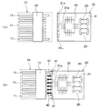
(第1実施形態)
図1は、本発明の第1実施形態に係るモールドパッケージの概略断面構成を示す図である。本実施形態のモールドパッケージは、大きくは、当該パッケージと外部とを接続するコネクタ10と、電子部品20が搭載された基板構造体30と、コネクタ10のピン11と基板構造体30とを電気的・機械的に接続する接続部材40と、これらコネクタ10および基板構造体30を封止するモールド樹脂50とを備えて構成されている。
(First embodiment)
FIG. 1 is a diagram showing a schematic cross-sectional configuration of a mold package according to a first embodiment of the present invention. The mold package of the present embodiment is broadly configured such that the
コネクタ10は、外部と接続される複数のピン11をコネクタハウジング12に設けてなる。ピン11は、銅やステンレスなどの導電性金属よりなる棒状のものであり、コネクタハウジング12は、PPS(ポリプロピレンサルファイド)やPBT(ポリブチレンテレフタレート)などの樹脂を成形してなるものである。
The
そして、本実施形態では、一般の汎用的なコネクタと同様に、各ピン11は、その長手方向の両端をコネクタハウジング12から露出させた状態で、コネクタハウジング12にインサート成型されて固定されている。
In this embodiment, each
基板構造体30は、本実施形態では、回路基板31と放熱板32とを積層したものよりなる。回路基板31は、この種の一般的なものであり、たとえばセラミック基板やプリント基板などよりなる。そして、回路基板31における放熱板32とは反対側の一面には、電子部品20が搭載されている。
In the present embodiment, the
電子部品20は、表面実装される電子部品であれば、特に限定されるものではないが、たとえば、マイコンなどのICチップ、MOSトランジスタなどのパワー素子、コンデンサやダイオードなどの受動素子が挙げられる。各電子部品20は、はんだや導電性接着剤などのダイマウント材あるいはワイヤボンド実装などによって、回路基板31の一面に搭載されている。
The
放熱板32は、回路基板31における電子部品20の搭載面とは反対側の他面に接着などにより接合されている。この放熱板32は、たとえば銅やアルミニウムなどの放熱性に優れた金属製の板材よりなるものであり、回路基板31からの熱を、外部に逃がす役割を果たすものである。
The
そして、コネクタ10においては、コネクタハウジング12から露出する各ピン11の一端が接続部材40を介して回路基板31に電気的・機械的に接続されており、他端は、たとえば外部の図示しない配線部材に接続されるようになっている。
In the
本実施形態では、接続部材40は、一般的なアルミニウムや金などよりなるボンディングワイヤ40であり、コネクタハウジング12から露出する各ピン11の一端と、回路基板31の一面における基板電極31aとが、ボンディングワイヤ40により結線されている。
In this embodiment, the
こうして、コネクタ10のピン11と回路基板31とが電気的・機械的に接続されてコネクタ10および基板構造体30が一体化されている。そして、本実施形態では、これら接続部材40によって一体化したコネクタ10および基板構造体30は、一体化部材60として構成されている。
Thus, the
そして、モールド樹脂50は、この一体化部材60を封止しているが、コネクタ10については、ピン11における外部と接続される他端側がモールド樹脂50より露出し、放熱板32については、回路基板31との接合面の反対側の面である放熱面がモールド樹脂50より露出している。このモールド樹脂50は、この種の分野にて用いられる一般的なものであり、たとえばエポキシ樹脂などよりなり、後述する金型を用いたトランスファーモールド法によって成形されるものである。
The mold resin 50 seals the integrated
次に、本実施形態のモールドパッケージの製造方法について、図2を参照して述べる。図2は、本製造方法における成型工程を示す概略断面図である。まず、本製造方法では、コネクタ10と、電子部品20が搭載された基板構造体30とを用意する。
Next, a method for manufacturing the mold package of the present embodiment will be described with reference to FIG. FIG. 2 is a schematic cross-sectional view showing a molding step in the manufacturing method. First, in this manufacturing method, the
次に、コネクタ10のピン11と基板構造体30の回路基板31とを、図2に示されるように、隣り合わせて配置する。続いて、両部材11、31の間でワイヤボンディングを行い、上記ボンディングワイヤ40を形成することにより、両部材11、31を電気的・機械的に接続し、コネクタ10および基板構造体30を一体化した一体化部材60を形成する(一体化部材形成工程)。
Next, the
次に、図2に示されるように、この一体化部材60を金型100内に設置し、金型100内に上記モールド樹脂50を注入することにより、コネクタ10および基板構造体30をモールド樹脂50にて封止する(成型工程)。
Next, as shown in FIG. 2, the
ここで、金型100は、一般的なモールドパッケージ用の金型を基本構成としており、鉄系金属などの金属よりなる上型110と下型120と備えたものである。そして、これら上下型110、120の間に封止対象物である一体化部材60を介在させ、この一体化部材60を挟みつけるように、上下型110、120を締結などによって合致させる。そうすることで、金型100の内部にモールド樹脂50の外形に対応したキャビティを形成するものである。
Here, the
つまり、成型工程においては、一体化部材60を金型100内に設置したとき、金型100の内面が一体化部材60に接して押しつけられることとなる。本実施形態では、図2に示されるように、金型100はコネクタハウジング12に接し、コネクタハウジング12を押さえつけた状態でコネクタ10を金型100内に固定するようにしている。
That is, in the molding process, when the
具体的には、図2に示されるように、金型100の上型110の内面、下型120の内面のうち、それぞれコネクタハウジング12に対向する部位が、コネクタハウジング12に接している。ここで、もしこれら内面の部位が、直接コネクタハウジング12に接すると、金型100の押さえによる応力によって、コネクタハウジング12に割れやクラックが発生する恐れがある。
Specifically, as shown in FIG. 2, portions of the inner surface of the
そこで、本実施形態では、図2に示されるように、金型100のうちコネクタハウジング12に接する面に、当該応力を緩和する応力緩和部材200を設け、この応力緩和部材200を介して、金型100によるコネクタハウジング12の押さえつけを行うようにしている。
Therefore, in the present embodiment, as shown in FIG. 2, a
この応力緩和部材200は、金型100がコネクタハウジング12を押さえたときにコネクタハウジング12にかかる応力をコネクタハウジング12の破断強度未満に低減するものである。
The
特に限定するものではないが、たとえばPPSやPBTよりなるコネクタハウジング12の破断強度は約200MPaであるが、このとき、応力緩和部材200を介して加わる上記応力を、約120MPaとすれば、コネクタハウジング12の外側に樹脂バリが残らないものにできる。
Although not particularly limited, for example, the
具体的に、応力緩和部材200は、金型100よりも軟らかいシートであり、たとえばテトラフルオロエチレンやシリコーンゴムなどの樹脂で作成されたシートを、当該金型100の内面に貼り付けたものである。そして、このシートの材質や厚さを調整することにより、上記応力を適正値まで低減することができる。
Specifically, the
こうして、本製造方法の成型工程では、応力緩和部材200を介して金型100でコネクタハウジング12を押さえた状態にて、金型100内にモールド樹脂50を注入・充填することにより、モールド樹脂50による封止がなされる。その後は、金型100からワークを取り出せば、上記図1に示されるモールドパッケージができあがる。
Thus, in the molding process of the present manufacturing method, the
このように、本実施形態によれば、金型100よりも軟らかい材料などよりなる応力緩和部材200を設けて、コネクタハウジング12の破断強度未満で当該ハウジングを押さえつけるようにしている。
Thus, according to the present embodiment, the
言い換えれば、本成型工程では、金型100のうちコネクタハウジング12に接する面と、コネクタハウジング12との間に、応力緩和部材200を介在させ、金型100によって、コネクタハウジング12の破断強度未満の力で、コネクタハウジング12を押さえつけて固定する。
In other words, in this molding process, the
そのため、一体化部材60を金型100に設置したときに、コネクタハウジング12が金型100によって押さえつけられても、その押さえつけによる応力がコネクタハウジング12の破断強度未満となるので、コネクタハウジング12の割れ・クラックが防止される。
Therefore, even if the
(第2実施形態)
図3は、本発明の第2実施形態に係るモールドパッケージの製造方法における成型工程を示す概略断面図である。本実施形態の製造方法は、上記第1実施形態に比べて、成型工程に用いる応力緩和部材200の構成を変形したところが相違するものであり、ここでは、その相違点を中心に述べることとする。
(Second Embodiment)
FIG. 3 is a schematic cross-sectional view showing a molding process in the mold package manufacturing method according to the second embodiment of the present invention. The manufacturing method of this embodiment is different from the first embodiment in that the configuration of the
図3に示されるように、本実施形態では、応力緩和部材200は、コネクタハウジング12を押さえつける方向に弾性を有するバネ部材210を備えている。バネ部材210は、特に限定しないが、たとえば、巻きばねなどである。ここでは、金型100の上型110に設けられた応力緩和部材200について、バネ部材210を備えたものとしている。また、下型120については、上記第1実施形態と同様の応力緩和部材200である。
As shown in FIG. 3, in this embodiment, the
具体的に、上型110の応力緩和部材200においては、バネ部材210における弾性作用方向の一端側を、溶接などにより上型110の内面に接合し、他端側には、鉄系金属などよりなる押さえブロック220を接合している。
Specifically, in the
また、押さえブロック220は、コネクタハウジング12に接してこれを押さえるものであるが、その接する面には応力緩和シート230が貼り付けられている。この応力緩和シート230は上記第1実施形態の応力緩和部材200と同様のシートである。
Further, the holding
そして、本実施形態の成型工程においても、一体化部材60を挟んで上下型110、120を合致させて、金型100の組み付けを完了させ、その後、モールド樹脂50による封止を行うことで、上記図1と同様のモールドパッケージができあがる。
And also in the molding process of the present embodiment, the upper and
このとき金型100の組み付けが完了した状態では、下型120の応力緩和部材200については、上記第1実施形態と同様のであるが、上型110の応力緩和部材200については、コネクタハウジング12は、バネ部材210および応力緩和シート230によって上記応力が低減された状態で押さえつけられる。
At this time, in the state where the assembly of the
そして、本実施形態によっても、一体化部材60を金型100に設置したときに、コネクタハウジング12が金型100によって押さえつけられても、その押さえつけによる応力がコネクタハウジング12の破断強度未満となるので、コネクタハウジング12の割れ・クラックが防止される。
Even in this embodiment, even when the
(第3実施形態)
図4は、本発明の第3実施形態に係るモールドパッケージの製造方法における要部である一体化部材形成工程を示す概略平面図である。本実施形態は、上記第1および第2実施形態における一体化部材形成工程に特徴を持たせたものであり、その特徴部分を中心に述べることとする。なお、この図4および後述の図5、図6では、コネクタハウジング12の外形を破線にて示してある。
(Third embodiment)
FIG. 4 is a schematic plan view showing an integrated member forming step which is a main part in the method for manufacturing a mold package according to the third embodiment of the present invention. In the present embodiment, the integrated member forming step in the first and second embodiments is characterized, and the characteristic portion will be mainly described. In FIG. 4 and FIGS. 5 and 6 to be described later, the outer shape of the
図4に示されるように、一体化部材形成工程では、コネクタ10のピン11と基板構造体30の回路基板31とを電気的・機械的に接続してコネクタ10および基板構造体30を一体化した一体化部材60を形成する。
As shown in FIG. 4, in the integrated member forming step, the
ここで、本実施形態では、コネクタ10の複数のピン11のうち配列方向の両端に位置するものについて、他のものよりも回路基板31側に突出させて長くしておく。そして、図4(a)に示されるように、この両端のピン11と回路基板31の両端の基板電極31aとを、はんだ41を介して接合し、固定する。この両端のピン11における接続については、電気的接続に使っても、単に固定用としてダミーの接続として用いてもよい。
Here, in the present embodiment, among the plurality of
そして、このように両端のピン11によって、コネクタ10と回路基板31とを固定した上で、図4(b)に示されるように、他のピン11と基板電極31aとの間でワイヤボンディングを行い、ボンディングワイヤ40を形成する。以上が、本実施形態の一体化部材形成工程である。それにより、ワイヤボンディングの前に、コネクタ10と基板構造体30とが安定に接続された状態となり、ワイヤボンディングが行いやすくなる。
And after fixing the
(第4実施形態)
図5は、本発明の第4実施形態に係るモールドパッケージの製造方法における要部である一体化部材形成工程を示す工程図であり、(a)はコネクタ10を基板構造体30側から視た側面図、(b)、(c)は当工程におけるワークの概略平面図である。本実施形態も、上記第1および第2実施形態における一体化部材形成工程に特徴を持たせたものであり、その特徴部分を中心に述べることとする。
(Fourth embodiment)
FIGS. 5A and 5B are process diagrams showing an integrated member forming process which is a main part in the method for manufacturing a mold package according to the fourth embodiment of the present invention. FIG. 5A is a view of the
図5(a)に示されるように、本実施形態では、基板構造体30が嵌合されて固定される嵌合部13が設けられている。ここでは、嵌合部13は、コネクタハウジング12の内壁に設けられた回路基板31が挿入されて固定される爪部である。この場合、基板構造体30において回路基板31を放熱板32よりもコネクタ10側に突出させれば、回路基板31の嵌合部13への挿入が可能である。
As shown in FIG. 5A, in the present embodiment, a
そして、本実施形態の一体化部材形成工程では、図5(b)に示されるように、この嵌合部13に回路基板31を挿入して、コネクタ10と基板構造体30とを接合し、その後、図5(c)に示されるように、ピン11と基板電極31aとの間でワイヤボンディングを行い、ボンディングワイヤ40を形成する。
And in the integrated member formation process of this embodiment, as shown in Drawing 5 (b),
以上が、本実施形態の一体化部材形成工程である。この場合も、ワイヤボンディングの前に、コネクタ10と基板構造体30とが安定に接続された状態となり、ワイヤボンディングが行いやすくなる。
The above is the integrated member forming step of the present embodiment. Also in this case, the
また、一体化部材の形成において、予め嵌合部13を介してコネクタ10と基板構造体30とを接続して一体化し、その後、ピン11と基板構造体30との接続を行うことが可能になるので、作業の簡易化が可能となる。
Further, in forming the integrated member, the
(第5実施形態)
図6は、本発明の第5実施形態に係るモールドパッケージの製造方法における要部である一体化部材形成工程を示すワークの概略平面図である。
(Fifth embodiment)
FIG. 6 is a schematic plan view of a work showing an integrated member forming step which is a main part in the method for manufacturing a mold package according to the fifth embodiment of the present invention.
上記各実施形態では、ピン11と回路基板31との接続をワイヤボンディングによって行っていたが、図6に示されるように、この接続を、すべてのピン11について、はんだ41を介して行ってもよい。
In each of the embodiments described above, the connection between the
(第6実施形態)
図7は、本発明の第6実施形態に係るモールドパッケージのコネクタ10の単体構成を示す図であり、(a)は概略斜視図、(b)はピン11の長手方向に沿った概略断面図である。本実施形態は、上記各実施形態におけるコネクタ10に特徴を持たせたものであり、その特徴部分を中心に述べることとする。
(Sixth embodiment)
FIGS. 7A and 7B are diagrams showing a single unit configuration of the
図7に示される本実施形態のコネクタ10は、ワイヤボンディング専用のものであり、ピン11と基板構造体30の回路基板31とはボンディングワイヤ40により接続されるものである。
The
このコネクタ10においては、上記同様に、ピン11はコネクタハウジング12にインサート成形により取り付けられているが、ここでは、コネクタハウジング12に、ピン11におけるワイヤボンディング面とは反対側の面を支持する台座部14が設けられている。また、この台座部14にも、嵌合部13が設けられているが、ここでは、放熱板32が嵌合する穴である。
In this
これにより、ピン11のうちワイヤボンディングされる部分は宙に浮いている形態ではなく、台座部14に支持固定されている。そのため、本実施形態によれば、一体化部材形成工程で、ピン11と回路基板31とをワイヤボンディングするときに、ピン11が台座部14で安定に支持されるのでワイヤボンディングしやすくなる。また、この台座部14の上方に露出しているピン11のワイヤボンディング面は、ワイヤ40が結線されると共に、モールド樹脂50で封止される。
As a result, the portion of the
図8は、本実施形態のコネクタ10を用いたモールドパッケージの製造方法を示す工程図であり、ここでは、各工程におけるワークを断面的に示している。まず、図8(a)、(b)に示されるように、用意されたコネクタ10と基板構造体30とを、一体化部材形成工程に供する。
FIG. 8 is a process diagram showing a method of manufacturing a mold package using the
まず、図8(a)に示されるように、コネクタハウジング12の嵌合部13に、放熱板32の突出部分を嵌合し、コネクタ10と基板構造体30とを一体に固定する。次に、図8(b)に示されるように、回路基板31の基板電極31aとピン11との間をボンディングワイヤ40により結線し、電気的接続を行うと、一体化部材60ができあがる。
First, as shown in FIG. 8A, the protruding portion of the
次に、成型工程では、上記第1実施形態または第2実施形態と同様に、応力緩和部材200を有する金型100を用いて、一体化部材60をモールド樹脂50にて封止する。ここでは、図8(c)に示されるように、上記第2実施形態と同様のバネ部材210を有する応力緩和部材200を備えた金型100を用いているが、もちろん上記第1実施形態と同様の金型であってもかまわない。これにより、成型工程を行い、図8(d)に示されるように、本実施形態のモールドパッケージができあがる。
Next, in the molding step, the
(第7実施形態)
図9は、本発明の第7実施形態に係るモールドパッケージのコネクタ10のコネクタハウジング12の単体構成を示す図であり、(a)は概略斜視図、(b)はピン11の長手方向に沿った概略断面図、(c)は(a)を矢印A方向から視た概略側面図、(d)は(a)を矢印B方向から視た概略平面図である。なお、図9(d)ではコネクタハウジング12の内部の貫通穴15には識別のため便宜上、斜線ハッチングを施してある。
(Seventh embodiment)
FIGS. 9A and 9B are diagrams showing a single structure of the
また、図10は、本実施形態に係るモールドパッケージの概略断面構成を示す図である。本実施形態は、上記第1〜第5の各実施形態におけるモールドパッケージにおいて、コネクタ10が相違するものであり、その相違部分を中心に述べることとする。
FIG. 10 is a diagram showing a schematic cross-sectional configuration of the mold package according to the present embodiment. This embodiment is different from the molded package in the first to fifth embodiments in that the
図9に示されるように、本実施形態では、用意されるコネクタ10においては、コネクタハウジング12に、当該コネクタハウジング12を貫通する貫通穴15が設けられている。この貫通穴15の貫通方向は、図9(a)において、矢印A方向である。
As shown in FIG. 9, in the present embodiment, in the
そして、この貫通穴15において、ピン11が挿入されるようになっている。ここで、貫通穴15は、図9(b)、(d)における右側の部分、すなわち基板構造体30寄りの部分では、ピン11の数の分の穴が設けられ、各貫通穴15は、それぞれのピン11毎に仕切られて独立した穴となっている。
And in this through-
このように、貫通穴15は、個々のピン11に対応して複数個設けられているが、ここでは、貫通穴15は、図9(b)、(d)における左側の部分、すなわちピン11が外部と接続される側の部分に向かっていくと、途中から各穴の仕切りが無くなり、すべての貫通穴15が連通した状態、つまり、1つの大きな穴とされている。もちろん、各貫通穴15は、全ての部分で仕切られて独立した穴であってもよい。
As described above, a plurality of through
また、ピン11は、上記同様に棒状をなすものであり、その挿入形態は、ピン11が貫通穴15の内面とは隙間を有して挿入されるものとされている。そして、ピン11が挿入されたコネクタ10の形状、つまり本実施形態のモールドパッケージにおけるコネクタ10の最終形状は、図10に示されるものである。
In addition, the
すなわち、図10に示されるように、ピン11と貫通穴15との内面との隙間にはモールド樹脂50が充填されており、ピン11は、貫通穴15の内部にてモールド樹脂50によって封止されている。そのため、このモールド樹脂50によって、ピン11はコネクタハウジング12に固定されている。
That is, as shown in FIG. 10, the gap between the
また、図10に示されるように、ピン11の貫通穴15への挿入後の状態については、貫通穴15の両端の開口部からピン11の両端が露出している。ここでは、当該各開口部からピン11の一端、他端がそれぞれ突出している。
Further, as shown in FIG. 10, in the state after the
このことについて、図9を参照して述べると、図9(a)、(d)におけるコネクタハウジング12の右側が基板構造体30側に位置し、左側が外部側に位置するものとなる。そして、貫通穴15における当該基板構造体30側の開口部にて露出するピン11の一端が回路基板31に接続され、それとは反対の当該外部側の開口部にて露出するピン11の他端が外部に接続されるようになっている。
This will be described with reference to FIG. 9. The right side of the
さらに、図9、図10に示されるように、コネクタハウジング12には、貫通穴15の途中から分岐してコネクタハウジング12の外部に抜けるバイパス穴16が設けられている。図9(a)、(b)を参照すると、図中の左右方向に延びる貫通穴15の途中に分岐部16aがあり、バイパス穴16は、この分岐部16aから上方に延びてコネクタハウジング12の上面にて外部に開口している。
Further, as shown in FIGS. 9 and 10, the
このバイパス穴16は、1個の貫通穴15について独立した1個の穴として設けられていてもよいが、ここでは、後述するようにバイパス穴16にモールド樹脂50を流通させるため、通路面積が大きい方が好ましい。そのため、ここでは、各貫通穴15に跨って連通する1個の大きな穴としてバイパス穴16が構成されている。
The
次に、本実施形態のコネクタ10を用いたモールドパッケージの製造方法について、図11〜図13を参照して述べる。図11は、本製造方法においてピン11と回路基板31とをワイヤボンディング接続する一体化部材形成工程を示す工程図であり、ワークの概略平面構成を示している。図12は、本製造方法の成型工程における金型100のセットの詳細を示す概略断面図であり、また、図13は、同成型工程を示す工程図であるが、ワークの概略断面構成を示してあり、応力緩和部材200は省略してある。
Next, a method for manufacturing a molded package using the
図11に示されるように、一体化部材形成工程では、コネクタ10のピン11と基板構造体30の回路基板31とを電気的・機械的に接続してコネクタ10および基板構造体30を一体化した一体化部材60を形成する。
As shown in FIG. 11, in the integrated member forming step, the
ここでは、ピン11と回路基板31とをワイヤボンディングした後に、ピン11をコネクタハウジング12に挿入する。また、ここで行うワイヤボンディングは、全ピン11をワイヤボンディングするものでもよいが、上記第3実施形態に示したような両端のピン11ではんだ付けし、それ以外のピン11でワイヤボンディングする方法を採用する。
Here, after
まず、図11(a)に示されるように、一端側がタイバー11aで連結され両端のピン11が長く突出する複数のピン11を用意する。そして、図11(b)に示されるように、当該両端のピン11を回路基板31にはんだ付けした後、残りのピン11と基板電極31aとの間でワイヤボンディングを行い、ボンディングワイヤ40で結線する。
First, as shown in FIG. 11A, a plurality of
次に、図11(c)に示されるように、複数のピン11の配置が崩れないように、樹脂製テープなどの固定治具11bで複数のピン11を固定した上で、タイバー11aをカットする。なお、固定治具11bは、後述する成型工程でモールド封止した際、パッケージ内に残留しても問題ないもの、たとえばポリイミドなどの電気絶縁性の樹脂テープなどとする。
Next, as shown in FIG. 11 (c), the plurality of
そして、この複数のピン11を、上記図9に示される本実施形態のコネクタハウジング12の貫通穴15に対して、上述した形態となるように挿入する。こうして、一体化部材60ができあがる。
Then, the plurality of
次に、本製造方法では、成型工程を行う。図12に示されるように、上記第1実施形態と同様の応力緩和部材200を備えた金型100を用い、これに一体化部材60を設置する。
Next, in this manufacturing method, a molding process is performed. As shown in FIG. 12, a
ここでは、金型100は、上記第1実施形態と同様に、応力緩和部材200を備える上型110、下型120に加えて、さらに横型111、121を備えている。横型111、121は、上下型110、120の間に、上下型110、120の合致方向(積層方向)とは直交する方向に挿入して、同方向にてコネクタ10を押さえつけて固定するものであり、コネクタハウジング12に接する面には、上記応力緩和部材200が貼り付けられている。
Here, the
この横型111、121は、コネクタハウジング12における外部と接続される側の開口部に入り込み、その内面を押さえつけるようになっている。このとき、コネクタハウジング12の貫通穴15は、横型111、121にて閉塞される。また、横型111、121は、上型110側に位置する横上型111と下型120側に位置する横下型121とを合致させたものである。
The
そして、コネクタ10の各ピン11のうち回路基板31とは反対側にて貫通穴15から露出する部位は、これら横上型111と横下型121との間に挟みこまれ、支持固定されるようになっている。つまり、横型111、121はコネクタハウジング12を押さえつけるとともに、ピン11の整列板としての機能も有する。
The portion of each
そして、本実施形態の成型工程では、これら上下型110、120および横型111、121を合致させて、これらにより一体化部材60を挟みこむことで、一体化部材60を金型100にセットする。
In the molding process of the present embodiment, the upper and
次に、図13(a)に示されるように、モールド樹脂50を金型100に注入する。ここで、金型100には、キャビティ内の空気抜き穴としてのエアベント130、および、モールド樹脂50を注入する注入口としてのゲート140が設けられている。エアベント130は、コネクタハウジング12におけるバイパス穴16の開口部に連通して設けられ、ゲート140は基板構造体30側に設けられている。
Next, as shown in FIG. 13A, the
そして、ゲート140から金型100内に注入されたモールド樹脂50は、基板構造体30を封止しながら、コネクタ10へ向かう。その後、モールド樹脂50は、コネクタハウジング12の貫通穴15における基板構造体30側の開口部から、ピン11と貫通穴15の内面との隙間を流通し、分岐部16bからバイパス穴16を通ってエアベント130に排出される。
Then, the
このように、本実施形態の成型工程では、回路基板30と接続されているピン11の一端が露出する方の貫通穴15の開口部とバイパス穴16の外部への開口部との間に、モールド樹脂50を流通させることで、ピン11と貫通穴15の内面との隙間をモールド樹脂50にて充填する。それにより、貫通穴15の内部にて各ピン11がモールド樹脂50により封止されコネクタハウジング12に固定される。
Thus, in the molding process of the present embodiment, between the opening of the through
こうして、図13(b)に示されるように、モールド樹脂50の充填が完了する。その後は、モールド樹脂50で封止された一体化部材60を金型100から取り出し、図13(c)に示されるように、エアベント130およびゲート140によりはみ出した樹脂を、機械的に除去する。こうして、本実施形態のモールドパッケージが完成する。
Thus, as shown in FIG. 13B, the filling of the
本実施形態によれば、コネクタ10をモールド樹脂50で封止したときに、コネクタハウジング12とモールド樹脂50との間で剥離が発生しても、貫通穴15の内部にてピン11とコネクタハウジング12との間はモールド樹脂50で充填されているので、隣り合うピン11間にはモールド樹脂50が介在し、当該間のリークが防止できる。
According to the present embodiment, when the
ここで、図14は、本第7実施形態におけるモールドパッケージの製造方法における成型工程の他の例を示す工程図であり、ワークの概略断面構成を示している。本実施形態では、この図14に示される例を採用してもよい。 Here, FIG. 14 is a process diagram illustrating another example of the molding process in the mold package manufacturing method according to the seventh embodiment, and shows a schematic cross-sectional configuration of a workpiece. In the present embodiment, the example shown in FIG. 14 may be adopted.
この例では、上記図12、図13に示される例とは金型100内のモールド樹脂50の流れ方向を逆にしたものである。すなわち、図14に示される例では、金型100において、コネクタハウジング12におけるバイパス穴16の開口部に連通するようにゲート140を設け、基板構造体30側にエアベント130を設けている。
In this example, the flow direction of the
そして、ゲート140から金型100内に注入されたモールド樹脂50は、バイパス穴16からコネクタハウジング12内に入り、ピン11と貫通穴15の内面との隙間を流通し、コネクタハウジング12の貫通穴15における基板構造体30側の開口部から基板構造体30側へ抜け、その後、基板構造体30を封止しながらエアベント130から排出される。
The
この例においても、回路基板30と接続されているピン11の一端が露出する方の貫通穴15の開口部とバイパス穴16の外部への開口部との間に、モールド樹脂50が流通することで、ピン11と貫通穴15の内面との隙間がモールド樹脂50にて充填され、固定される。こうして、本例においても、モールド樹脂50の充填が完了し、その後は、上記同様に、はみ出し樹脂の除去を行うことにより、本実施形態のモールドパッケージが完成する。
Also in this example, the
また、図15は、本第7実施形態におけるモールドパッケージの製造方法の成型工程における金型100の他の例を示す概略断面図である。この金型100では、上記第2実施形態と同様のバネ部材210を有する応力緩和部材200を備えた金型100を用い、これに対して、上記横型111、121を付加した構成とされている。この図15に示される金型100を採用しても、同様の効果が得られる。
FIG. 15 is a schematic cross-sectional view showing another example of the
(第8実施形態)
図16は、本発明の第8実施形態に係るモールドパッケージの概略断面構成を示す図であり、図17は、本実施形態のモールドパッケージの製造方法における一体化部材形成工程を示す工程図であり、ワークの概略平面構成を示している。
(Eighth embodiment)
FIG. 16 is a diagram showing a schematic cross-sectional configuration of a mold package according to an eighth embodiment of the present invention, and FIG. 17 is a process diagram showing an integrated member forming process in the mold package manufacturing method of the present embodiment. 1 shows a schematic plane configuration of a workpiece.
本実施形態は、上記第7実施形態と同様のコネクタ10を用いるが、ピン11と回路基板31との接続を、ワイヤボンディングではなく、はんだ付けとしたところが、上記第7実施形態の一体化部材形成工程と相違するものである。この相違点を中心に述べる。
This embodiment uses the
図16に示されるように、本実施形態では、コネクタ10において、コネクタハウジング12の貫通穴15に挿入されたピン11は、その一端が当該貫通穴15における基板構造体30側の開口部より突出して露出し、回路基板31に対して、はんだ41により電気的・機械的に接続されている。
As shown in FIG. 16, in this embodiment, in the
本実施形態の一体化部材形成工程について、図17を参照して述べる。ここでは、ピン11と回路基板31とをはんだ付けした後に、ピン11をコネクタハウジング12に挿入する。
The integrated member forming process of this embodiment will be described with reference to FIG. Here, after the
まず、図17(a)に示されるように、一端側がタイバー11aで連結された複数のピン11を用意する。そして、図17(b)に示されるように、各ピン11を回路基板31にはんだ付けする。
First, as shown in FIG. 17A, a plurality of
次に、図17(c)に示されるように、タイバー11aをカットする。そして、この複数のピン11を、コネクタハウジング12の貫通穴15に対して挿入すると、一体化部材60ができあがる。
Next, as shown in FIG. 17C, the
次に、本製造方法では、上記第1実施形態または上記第2実施形態と同様の応力緩和部材200を備えた金型100を用いて、上記第7実施形態と同様に、成型工程を行う。そして、成型工程を終え、モールド樹脂50の充填が完了した後は、上記同様に、はみ出した樹脂の除去を行うことにより、本実施形態のモールドパッケージが完成する。
Next, in the present manufacturing method, a molding process is performed in the same manner as in the seventh embodiment, using the
このように、本第8に実施形態おいては、ピン11と回路基板31との接続を、はんだ付けにより行っているが、この場合にも、上記第7実施形態と同様に、コネクタハウジング12とモールド樹脂50との間で剥離が発生しても、隣り合うピン11間のリークが防止できる。また、本実施形態も上記第1〜第5実施形態に採用できる。
Thus, in the eighth embodiment, the connection between the
(第9実施形態)
図18は、本発明の第9実施形態に係るモールドパッケージの製造方法における一体化部材形成工程を示す工程図であり、(a)、(b)はワイヤボンディング前のワークにおけるそれぞれ概略断面図、概略平面図であり、(c)、(d)はワイヤボンディング後のワークにおけるそれぞれ概略断面図、概略平面図である。
(Ninth embodiment)
FIG. 18 is a process diagram showing an integrated member forming process in the mold package manufacturing method according to the ninth embodiment of the present invention, wherein (a) and (b) are schematic cross-sectional views of the work before wire bonding, It is a schematic plan view, and (c) and (d) are a schematic sectional view and a schematic plan view, respectively, of the workpiece after wire bonding.
本実施形態は、上記第7実施形態と同様のコネクタ10を用いるが、ピン11をコネクタハウジング12の貫通穴15に挿入した後、ピン11と回路基板31とをワイヤボンディングにより接続するところが、上記第7実施形態の一体化部材形成工程と相違するものである。この相違点を中心に述べる。
This embodiment uses the
まず、本実施形態では、図18(a)、(b)に示されるように、一端側がタイバー11aで連結された複数のピン11を用意し、これをコネクタハウジング12の貫通穴15に挿入する。この場合、上記第7実施形態とは逆に、貫通穴15における基板構造体30側とは反対側の開口部よりピン11を挿入する。そして、基板構造体30の放熱板32とコネクタハウジング12とを接着などにより固定する。
First, in the present embodiment, as shown in FIGS. 18A and 18B, a plurality of
次に、図18(c)、(d)に示されるように、ピン11と回路基板31との間でワイヤボンディングを行い、ボンディングワイヤ40による接続を完成させる。その後、タイバー11aをカットすると、一体化部材60ができあがる。
Next, as shown in FIGS. 18C and 18D, wire bonding is performed between the
次に、本製造方法では、上記第1実施形態または上記第2実施形態と同様の応力緩和部材200を備えた金型100に一体化部材60を設置し、上記第7実施形態と同様に、成型工程を行う。その後、上記同様に、はみ出した樹脂の除去を行うことにより、本実施形態のモールドパッケージが完成する。
Next, in this manufacturing method, the
そして、本第9に実施形態おいても、上記第7実施形態と同様に、コネクタハウジング12とモールド樹脂50との間で剥離が発生しても、隣り合うピン11間のリークが防止できる。また、本実施形態も上記第1〜第5実施形態に採用できる。
In the ninth embodiment, as in the seventh embodiment, even if peeling occurs between the
(第10実施形態)
図19は、本発明の第10実施形態に係るモールドパッケージの要部を示す概略平面図であり、コネクタ10を基板構造体30側から見たときの種々のピン11の配置構成を示している。本実施形態は、上記第7実施形態のコネクタ10を用いるものである。
(10th Embodiment)
FIG. 19 is a schematic plan view showing the main part of the mold package according to the tenth embodiment of the present invention, and shows the arrangement of
上記各実施形態におけるコネクタ10におけるピン11の配置形態としては、図19(a)に示される1列配置、図19(b)に示される2列マトリックス配置、図19(c)に示される2列千鳥配置、図19(d)に示されるn列マトリックス配置(n:3以上の自然数)、図19(e)に示されるn列千鳥配置などが採用可能である。
As the arrangement form of the
また、図20は、本実施形態において、上記図19(b)〜(e)に示されるような複数列配置のピン11の場合におけるピン11と回路基板31との接続構成を示す概略側面図であり、(a)は、はんだ付けの場合、(b)は、ワイヤボンディングの場合を示す。図20に示されるように、複数配列の場合には、ピン11を折り曲げたり、回路基板31上の接続位置を各列でずらしたりすればよい。
FIG. 20 is a schematic side view showing a connection configuration between the
(第11実施形態)
図21は、本発明の第11実施形態に係るモールドパッケージの製造方法における成型工程を示す工程図であり、(a)はワークの概略断面図、(b)、(c)は(a)中のD部拡大図である。
(Eleventh embodiment)
FIG. 21 is a process diagram showing a molding process in the mold package manufacturing method according to the eleventh embodiment of the present invention, in which (a) is a schematic sectional view of a workpiece, and (b) and (c) are in (a). FIG.
本実施形態は、上記第1実施形態に比べて、応力緩和部材200とその周辺部の構成を変形したところが相違するものであり、ここでは、その相違点を中心に述べることとする。
The present embodiment is different from the first embodiment in that the
図21に示されるように、本実施形態では、金型100の上型110の内面のうちコネクタハウジング12に対向する部位に、突起100aを設け、この突起100aに対向するコネクタハウジング12の面に凹部12aを設け、凹部12a内に応力緩和部材200としてシリコーンゴムを配置しておく。
As shown in FIG. 21, in the present embodiment, a protrusion 100a is provided on a portion of the inner surface of the
そして、成型工程では、図21(b)から図21(c)に示されるように、突起100aを凹部12aに応力緩和部材200を介して噛みこませることで、上型110によるコネクタハウジング12の押さえつけ固定を行う。なお、図示しない下型については、上記第1実施形態と同様である。こうして、モールド樹脂50による一体化部材60の封止を行う。
In the molding process, as shown in FIGS. 21B to 21C, the protrusion 100a is engaged with the
ここで、上型110の内面については、コネクタハウジング12を押さえる部位は突起100aだけであり、その他の部位はコネクタハウジング12に接することはない。そこで、コネクタハウジング12のうち突起100aに対応して凹部12aを設ける部位は厚肉部であることが望ましい。つまり、コネクタハウジング12に厚肉部とそれよりも肉薄の薄肉部とが存在する場合、凹部12aは薄肉部に設けることが好ましい。
Here, with respect to the inner surface of the
(第12実施形態)
図22は、本発明の第12実施形態に係るモールドパッケージの要部を示す図であり、種々の断面形状を有するピン11の断面構成を示す図である。また、図23は、本実施形態におけるコネクタハウジング12の貫通穴15の種々の穴断面形状を示す断面図である。本実施形態は、コネクタとしては上記第7実施形態に示したコネクタ10を対象としている。
(Twelfth embodiment)
FIG. 22 is a view showing the main part of the mold package according to the twelfth embodiment of the present invention, and is a view showing the cross-sectional configurations of the
棒状をなすピン11の長手方向と直交する断面形状としては、図22に示されるように、(a)円形、(b)四角形、(c)六角形、またはそれ以外の多角形など種々の形状が可能である。
As shown in FIG. 22, the cross-sectional shape orthogonal to the longitudinal direction of the
また、貫通穴15の穴断面形状としては、貫通穴15の内面とピン11との間に隙間を有するものであればよく、図23(a)〜(g)に示されるように、種々の形状が可能である。また、ピン11の形状としては、ピン11の外面と貫通穴15の内面とが数点接触し、ピン11の位置がずれないようなものが望ましい。
Moreover, as a hole cross-sectional shape of the through-
(第13実施形態)
図24は、本発明の第13実施形態に係るモールドパッケージの要部を示す概略断面図であり、コネクタハウジング12の貫通穴15におけるバイパス穴16の分岐部16a付近の拡大図である。本実施形態は、上記第7実施形態に示したコネクタ10に対して、組み合わせて適用することが可能であり、ここでは、上記第7実施形態との相違点を中心に述べることとする。
(13th Embodiment)
FIG. 24 is a schematic cross-sectional view showing the main part of the mold package according to the thirteenth embodiment of the present invention, and is an enlarged view of the vicinity of the
図24に示されるように、本実施形態では、用意されるコネクタ10において、貫通穴15のうちバイパス穴16が分岐する部分である分岐部16aとピン11の他端が露出する方の開口部との間の部位で、ピン11が貫通穴15の内面に接触して貫通穴15を閉塞している。
As shown in FIG. 24, in the present embodiment, in the
ここでは、ピン11として、回路基板31に接続される一端側から外部に接続される他端側に向かってテーパ状に細くなっているものを用いる。一方、貫通穴15についても、ピン11の一端が露出する方の開口部から分岐部16aまでの部分と、分岐部16aからピン11の他端が露出する方の開口部までの部分とでは、前者の方を後者よりも穴が広いものとすることで、貫通穴15による上記閉塞を実現している。
Here, as the
そして、本実施形態の成型工程では、ピン11の一端が露出する方の貫通穴15の開口部とバイパス穴16の外部への開口部との間に、モールド樹脂50が流通する。このとき、貫通穴15による閉塞部では、貫通穴15内を流通するモールド樹脂50は止められる。そのため、貫通穴15のうちピン11の他端が露出する方の開口部から貫通穴15の外部へモールド樹脂50が流出するのを防止できる。
In the molding process of this embodiment, the
また、図25は、本第13実施形態の他の例を示す図であり、(a)は概略断面図、(b)、(c)は(a)中のピン11の種々の断面形状を示す図である。この例では、ピン11は長手方向に均一な太さであって、上記閉塞部を形成する部位にて外面より径方向に突出するツバ部11bを有するものである。この場合も、ツバ部11bが貫通穴15を閉塞するため、上記同様、閉塞部によるモールド樹脂50の流出防止がなされる。
FIG. 25 is a diagram showing another example of the thirteenth embodiment, in which (a) is a schematic cross-sectional view, and (b) and (c) are various cross-sectional shapes of the
(第14実施形態)
図26は、本発明の第14実施形態に係るコネクタ10の概略断面構成を示す図である。本実施形態は、上記第7実施形態に示したコネクタ10に対してポッティング樹脂17を付加したところが相違するものであり、ここでは、その相違点を中心に述べることとする。
(14th Embodiment)
FIG. 26 is a diagram showing a schematic cross-sectional configuration of the
図26に示されるように、本実施形態では、コネクタハウジング12にピン11を挿入した後であって、成型工程に供する前に、コネクタハウジング12における貫通穴15のうちピン11の他端が露出する方の開口部に、エポキシ樹脂などのポッティング樹脂17を塗布・硬化して設け、当該開口部を封止するものである。
As shown in FIG. 26, in this embodiment, after the
この場合、ポッティング樹脂17の配設により、各ピン11が固定されて位置ずれしにくくなる。また、成型工程のときに、このポッティング樹脂17が上記第13実施形態と同様の閉塞部の効果を奏し、貫通穴15のうちピン11の他端が露出する方の開口部から貫通穴15の外部へモールド樹脂50が流出するのを防止できる。
In this case, due to the arrangement of the potting
(第15実施形態)
図27(a)および(b)は、本発明の第15実施形態に係る要部の概略断面構成を示す図である。本実施形態は、上記各実施形態のうちピン11と基板構造体30とをはんだ付けにより電気的・機械的に接続する場合において、ピン11の形状を変形させたものである。
(Fifteenth embodiment)
FIGS. 27A and 27B are diagrams showing a schematic cross-sectional configuration of the main part according to the fifteenth embodiment of the present invention. In the present embodiment, the shape of the
本実施形態では、ピン11の途中部分を曲げたり(図27(a)参照)、ピン11の途中部分にくぼみを形成した(図27(b)参照)ものである。それにより、たとえばコネクタハウジング12の上記嵌合部13に基板構造体30を嵌合した時の力が、はんだ付け部分に影響するのを回避することが可能となる。
In the present embodiment, the middle portion of the
(第16実施形態)
図28は、本発明の第16実施形態に係る一体化部材60の概略断面構成を示す図である。本実施形態は、上記第7実施形態に示したコネクタ10において、コネクタハウジング12に嵌合部13を設けたものであり、この場合にも、当該嵌合部13による効果は上記同様である。
(Sixteenth embodiment)
FIG. 28 is a diagram showing a schematic cross-sectional configuration of an
(他の実施形態)
なお、上記各実施形態では、基板構造体は、回路基板と放熱板とを積層したものであったが、基板構造体としては、電子部品が搭載可能であってコネクタと電気的・機械的に接続可能なものであればよく、たとえば回路基板だけであってもよい。また、リードフレームなどであってもよい。
(Other embodiments)
In each of the above embodiments, the board structure is a laminate of a circuit board and a heat sink. However, as the board structure, an electronic component can be mounted and the connector is electrically and mechanically. Any circuit can be used as long as it can be connected. Further, it may be a lead frame or the like.
また、応力緩和部材200は、上記各実施形態では、金型100の内面にあらかじめ貼り付けていたが、それとは逆に、あらかじめ一体化部材60におけるコネクタハウジング12の外面に上記シート状の応力緩和部材200を貼り付けた後、これを金型100内に設置するようにしてもよい。
In each of the above embodiments, the
10 コネクタ
11 ピン
12 コネクタハウジング
13 嵌合部
14 台座部
15 貫通穴
16 バイパス穴
16a 分岐部
30 基板構造体
50 モールド樹脂
60 一体化部材
100 金型
200 応力緩和部材
210 バネ部材
DESCRIPTION OF
Claims (7)
前記コネクタ(10)の前記ピン(11)と前記基板構造体(30)とを電気的・機械的に接続して前記コネクタ(10)および前記基板構造体(30)を一体化した一体化部材(60)を形成する一体化部材形成工程と、
前記一体化部材(60)を金型(100)内に設置し、前記金型(100)内にモールド樹脂(50)を注入することにより、前記コネクタ(10)および前記基板構造体(30)を前記モールド樹脂(50)にて封止する成型工程と、を備えるモールドパッケージの製造方法であって、
前記一体化部材(60)を前記金型(100)内に設置したとき、前記金型(100)は前記コネクタハウジング(12)に接してこれを押さえつけた状態で前記コネクタ(10)を前記金型(100)内に固定するものであり、
前記金型(100)のうち前記コネクタハウジング(12)に接する面に、前記金型(100)が前記コネクタハウジング(12)を押さえたときに前記コネクタハウジング(12)にかかる応力を前記コネクタハウジング(12)の破断強度未満に低減する応力緩和部材(200)を設け、この応力緩和部材(200)を介して、前記金型(100)による押さえつけを行うことを特徴とするモールドパッケージの製造方法。 A connector (10) provided with a plurality of pins (11) connected to the outside in a connector housing (12) made of resin, and a substrate structure (30) on which an electronic component (20) is mounted are prepared,
An integrated member in which the connector (10) and the board structure (30) are integrated by electrically and mechanically connecting the pins (11) of the connector (10) and the board structure (30). An integrated member forming step of forming (60);
The integrated member (60) is installed in the mold (100), and a mold resin (50) is injected into the mold (100), whereby the connector (10) and the substrate structure (30). And a molding step of sealing the mold resin (50) with a mold package,
When the integrated member (60) is installed in the mold (100), the mold (100) contacts the connector housing (12) and presses the connector (10) with the mold (100). Fixed in the mold (100),
A stress applied to the connector housing (12) when the mold (100) presses the connector housing (12) on a surface of the mold (100) that contacts the connector housing (12). A method of manufacturing a mold package, comprising: providing a stress relaxation member (200) that is reduced to less than the breaking strength of (12), and pressing the mold (100) through the stress relaxation member (200). .
前記成型工程では、前記ピン(11)の前記一端が露出する方の前記貫通穴(15)の前記開口部と前記バイパス穴(16)の外部への開口部との間に前記モールド樹脂(50)を流通させて、前記ピン(11)と前記貫通穴(15)の内面との隙間を前記モールド樹脂(50)にて充填することを特徴とする請求項1に記載のモールドパッケージの製造方法。 In the prepared connector (10), the connector housing (12) has a hole penetrating the connector housing (12), and the pin (11) having a rod shape has a gap with the inner surface of the hole. Through holes (15) are provided, both ends of the pins (11) are exposed from openings at both ends of the through holes (15), and one end of the pins (11) is connected to the substrate structure (30). ) And the other end of the pin (11) is connected to the outside. Further, the connector housing (12) branches off from the middle of the through hole (15) and the connector housing ( 12) is provided with a bypass hole (16) that goes outside
In the molding step, the mold resin (50) is formed between the opening of the through hole (15) on which the one end of the pin (11) is exposed and the opening to the outside of the bypass hole (16). The mold package manufacturing method according to claim 1, wherein a gap between the pin (11) and the inner surface of the through hole (15) is filled with the mold resin (50). .
前記成型工程では、前記貫通穴(15)の閉塞部によって、前記貫通穴(15)のうち前記ピン(11)の前記他端が露出する方の開口部から前記モールド樹脂(50)が流出するのを防止していることを特徴とする請求項2に記載のモールドパッケージの製造方法。 In the prepared connector (10), between the through hole (15), the branch part (16a) of the bypass hole (16) and the opening part where the other end of the pin (11) is exposed. The pin (11) is in contact with the through hole (15) and closes the through hole (15),
In the molding step, the mold resin (50) flows out from the opening of the through hole (15) where the other end of the pin (11) is exposed by the blocking portion of the through hole (15). The method of manufacturing a mold package according to claim 2, wherein
Priority Applications (1)
| Application Number | Priority Date | Filing Date | Title |
|---|---|---|---|
| JP2008267232A JP5056717B2 (en) | 2008-10-16 | 2008-10-16 | Mold package manufacturing method |
Applications Claiming Priority (1)
| Application Number | Priority Date | Filing Date | Title |
|---|---|---|---|
| JP2008267232A JP5056717B2 (en) | 2008-10-16 | 2008-10-16 | Mold package manufacturing method |
Publications (2)
| Publication Number | Publication Date |
|---|---|
| JP2010098097A true JP2010098097A (en) | 2010-04-30 |
| JP5056717B2 JP5056717B2 (en) | 2012-10-24 |
Family
ID=42259582
Family Applications (1)
| Application Number | Title | Priority Date | Filing Date |
|---|---|---|---|
| JP2008267232A Expired - Fee Related JP5056717B2 (en) | 2008-10-16 | 2008-10-16 | Mold package manufacturing method |
Country Status (1)
| Country | Link |
|---|---|
| JP (1) | JP5056717B2 (en) |
Cited By (8)
| Publication number | Priority date | Publication date | Assignee | Title |
|---|---|---|---|---|
| JP2012099628A (en) * | 2010-11-02 | 2012-05-24 | Towa Corp | Resin seal molding method and device of electric circuit component |
| JP2019009295A (en) * | 2017-06-26 | 2019-01-17 | 三菱電機株式会社 | Semiconductor device |
| WO2020008817A1 (en) * | 2018-07-05 | 2020-01-09 | 日立オートモティブシステムズ株式会社 | Resin-sealed onboard electronic control device |
| CN111293043A (en) * | 2018-12-07 | 2020-06-16 | 富士电机株式会社 | Manufacturing method of semiconductor device and semiconductor device |
| US10861758B2 (en) | 2018-07-31 | 2020-12-08 | Mitsubishi Electric Corporation | Semiconductor device, power conversion apparatus, and method of manufacturing semiconductor device |
| WO2021177426A1 (en) * | 2020-03-06 | 2021-09-10 | 株式会社オートネットワーク技術研究所 | Connector device |
| WO2021177427A1 (en) * | 2020-03-06 | 2021-09-10 | 株式会社オートネットワーク技術研究所 | Connector device and method for manufacturing connector device |
| CN114932514A (en) * | 2022-07-01 | 2022-08-23 | 青岛凯瑞电子有限公司 | Accurate positioning and machining device for anti-cracking die filling of ceramic shell |
Citations (2)
| Publication number | Priority date | Publication date | Assignee | Title |
|---|---|---|---|---|
| JPH1076528A (en) * | 1996-09-03 | 1998-03-24 | Fujitsu Ten Ltd | Mold structure and connector structure |
| JP2004111435A (en) * | 2002-09-13 | 2004-04-08 | Hitachi Ltd | Electric/electronic module having integral molding structure of connector and electronic part and method for molding the same |
-
2008
- 2008-10-16 JP JP2008267232A patent/JP5056717B2/en not_active Expired - Fee Related
Patent Citations (2)
| Publication number | Priority date | Publication date | Assignee | Title |
|---|---|---|---|---|
| JPH1076528A (en) * | 1996-09-03 | 1998-03-24 | Fujitsu Ten Ltd | Mold structure and connector structure |
| JP2004111435A (en) * | 2002-09-13 | 2004-04-08 | Hitachi Ltd | Electric/electronic module having integral molding structure of connector and electronic part and method for molding the same |
Cited By (17)
| Publication number | Priority date | Publication date | Assignee | Title |
|---|---|---|---|---|
| JP2012099628A (en) * | 2010-11-02 | 2012-05-24 | Towa Corp | Resin seal molding method and device of electric circuit component |
| JP2019009295A (en) * | 2017-06-26 | 2019-01-17 | 三菱電機株式会社 | Semiconductor device |
| US11069593B2 (en) | 2017-06-26 | 2021-07-20 | Mitsubishi Electric Corporation | Semiconductor device |
| JP7232582B2 (en) | 2018-07-05 | 2023-03-03 | 日立Astemo株式会社 | Resin-encapsulated in-vehicle electronic control unit |
| WO2020008817A1 (en) * | 2018-07-05 | 2020-01-09 | 日立オートモティブシステムズ株式会社 | Resin-sealed onboard electronic control device |
| JP2020009852A (en) * | 2018-07-05 | 2020-01-16 | 日立オートモティブシステムズ株式会社 | Resin seal on-vehicle electronic controller |
| CN112352474A (en) * | 2018-07-05 | 2021-02-09 | 日立汽车系统株式会社 | Resin-sealed vehicle-mounted electronic control device |
| CN112352474B (en) * | 2018-07-05 | 2024-04-26 | 日立安斯泰莫株式会社 | Resin sealed vehicle-mounted electronic control device |
| US10861758B2 (en) | 2018-07-31 | 2020-12-08 | Mitsubishi Electric Corporation | Semiconductor device, power conversion apparatus, and method of manufacturing semiconductor device |
| CN111293043A (en) * | 2018-12-07 | 2020-06-16 | 富士电机株式会社 | Manufacturing method of semiconductor device and semiconductor device |
| WO2021177426A1 (en) * | 2020-03-06 | 2021-09-10 | 株式会社オートネットワーク技術研究所 | Connector device |
| JP2021141002A (en) * | 2020-03-06 | 2021-09-16 | 株式会社オートネットワーク技術研究所 | Connector device and manufacturing method of connector device |
| JP2021141001A (en) * | 2020-03-06 | 2021-09-16 | 株式会社オートネットワーク技術研究所 | Connector device |
| WO2021177427A1 (en) * | 2020-03-06 | 2021-09-10 | 株式会社オートネットワーク技術研究所 | Connector device and method for manufacturing connector device |
| US12212091B2 (en) | 2020-03-06 | 2025-01-28 | Autonetworks Technologies, Ltd. | Electrical connector apparatus with improved waterproofing and compact size and method of manufacturing thereof |
| CN114932514A (en) * | 2022-07-01 | 2022-08-23 | 青岛凯瑞电子有限公司 | Accurate positioning and machining device for anti-cracking die filling of ceramic shell |
| CN114932514B (en) * | 2022-07-01 | 2023-08-25 | 青岛凯瑞电子有限公司 | Accurate positioning processing device for cracking-preventing die-filling of ceramic shell |
Also Published As
| Publication number | Publication date |
|---|---|
| JP5056717B2 (en) | 2012-10-24 |
Similar Documents
| Publication | Publication Date | Title |
|---|---|---|
| JP5056717B2 (en) | Mold package manufacturing method | |
| JP3793628B2 (en) | Resin-sealed semiconductor device | |
| JP5252819B2 (en) | Semiconductor device and manufacturing method thereof | |
| US9887142B2 (en) | Power semiconductor device | |
| KR100730826B1 (en) | Semiconductor package and lead frame therefor | |
| US7772036B2 (en) | Lead frame based, over-molded semiconductor package with integrated through hole technology (THT) heat spreader pin(s) and associated method of manufacturing | |
| CN104167370B (en) | Manufacturing method for semiconductor device and semiconductor device | |
| JP2003017518A (en) | Method for manufacturing hybrid integrated circuit device | |
| CN105814682B (en) | Semiconductor device | |
| JP4614584B2 (en) | Hybrid integrated circuit device and manufacturing method thereof | |
| US20170345742A1 (en) | Semiconductor device and manufacturing method thereof | |
| US9305829B2 (en) | Semiconductor package with an indented portion and manufacturing method thereof | |
| JP4334335B2 (en) | Method for manufacturing hybrid integrated circuit device | |
| US20170141022A1 (en) | Semiconductor device and method of manufacturing semiconductor device | |
| JP2006279088A (en) | Method for manufacturing semiconductor device | |
| CN110164843B (en) | Lead frame, lead frame with resin, method for manufacturing lead frame with resin, and method for manufacturing semiconductor device | |
| JP4887346B2 (en) | Semiconductor device | |
| JP4534675B2 (en) | Integrated circuit device | |
| JP4760543B2 (en) | Mold package and manufacturing method thereof | |
| JP5093076B2 (en) | Mold package and manufacturing method thereof | |
| JP5145596B2 (en) | Semiconductor device | |
| JP5408039B2 (en) | Electronic equipment | |
| JP2024046328A (en) | semiconductor equipment | |
| JP5109740B2 (en) | Electronic device and manufacturing method thereof | |
| JP2023152323A (en) | Semiconductor device and method for manufacturing semiconductor device |
Legal Events
| Date | Code | Title | Description |
|---|---|---|---|
| A621 | Written request for application examination |
Free format text: JAPANESE INTERMEDIATE CODE: A621 Effective date: 20101202 |
|
| A977 | Report on retrieval |
Free format text: JAPANESE INTERMEDIATE CODE: A971007 Effective date: 20111207 |
|
| A131 | Notification of reasons for refusal |
Free format text: JAPANESE INTERMEDIATE CODE: A131 Effective date: 20111220 |
|
| A521 | Request for written amendment filed |
Free format text: JAPANESE INTERMEDIATE CODE: A523 Effective date: 20120213 |
|
| TRDD | Decision of grant or rejection written | ||
| A01 | Written decision to grant a patent or to grant a registration (utility model) |
Free format text: JAPANESE INTERMEDIATE CODE: A01 Effective date: 20120703 |
|
| A01 | Written decision to grant a patent or to grant a registration (utility model) |
Free format text: JAPANESE INTERMEDIATE CODE: A01 |
|
| A61 | First payment of annual fees (during grant procedure) |
Free format text: JAPANESE INTERMEDIATE CODE: A61 Effective date: 20120716 |
|
| FPAY | Renewal fee payment (event date is renewal date of database) |
Free format text: PAYMENT UNTIL: 20150810 Year of fee payment: 3 |
|
| FPAY | Renewal fee payment (event date is renewal date of database) |
Free format text: PAYMENT UNTIL: 20150810 Year of fee payment: 3 |
|
| LAPS | Cancellation because of no payment of annual fees |