JP2010035271A - Power converter - Google Patents
Power converter Download PDFInfo
- Publication number
- JP2010035271A JP2010035271A JP2008192116A JP2008192116A JP2010035271A JP 2010035271 A JP2010035271 A JP 2010035271A JP 2008192116 A JP2008192116 A JP 2008192116A JP 2008192116 A JP2008192116 A JP 2008192116A JP 2010035271 A JP2010035271 A JP 2010035271A
- Authority
- JP
- Japan
- Prior art keywords
- converter
- voltage
- transformer
- power
- circuit
- Prior art date
- Legal status (The legal status is an assumption and is not a legal conclusion. Google has not performed a legal analysis and makes no representation as to the accuracy of the status listed.)
- Pending
Links
- 238000006243 chemical reaction Methods 0.000 claims abstract description 62
- 238000001514 detection method Methods 0.000 claims abstract description 34
- 230000008054 signal transmission Effects 0.000 claims abstract description 13
- 238000010586 diagram Methods 0.000 description 32
- 239000004973 liquid crystal related substance Substances 0.000 description 31
- 238000004804 winding Methods 0.000 description 11
- 239000003990 capacitor Substances 0.000 description 10
- 238000000034 method Methods 0.000 description 8
- 230000000694 effects Effects 0.000 description 6
- 238000009413 insulation Methods 0.000 description 4
- 238000009499 grossing Methods 0.000 description 3
- 239000004575 stone Substances 0.000 description 2
- 239000004020 conductor Substances 0.000 description 1
- 238000005516 engineering process Methods 0.000 description 1
- 230000004907 flux Effects 0.000 description 1
- 230000002093 peripheral effect Effects 0.000 description 1
Images


Classifications
-
- H—ELECTRICITY
- H05—ELECTRIC TECHNIQUES NOT OTHERWISE PROVIDED FOR
- H05B—ELECTRIC HEATING; ELECTRIC LIGHT SOURCES NOT OTHERWISE PROVIDED FOR; CIRCUIT ARRANGEMENTS FOR ELECTRIC LIGHT SOURCES, IN GENERAL
- H05B45/00—Circuit arrangements for operating light-emitting diodes [LED]
- H05B45/30—Driver circuits
- H05B45/37—Converter circuits
- H05B45/3725—Switched mode power supply [SMPS]
- H05B45/38—Switched mode power supply [SMPS] using boost topology
-
- H—ELECTRICITY
- H05—ELECTRIC TECHNIQUES NOT OTHERWISE PROVIDED FOR
- H05B—ELECTRIC HEATING; ELECTRIC LIGHT SOURCES NOT OTHERWISE PROVIDED FOR; CIRCUIT ARRANGEMENTS FOR ELECTRIC LIGHT SOURCES, IN GENERAL
- H05B45/00—Circuit arrangements for operating light-emitting diodes [LED]
- H05B45/30—Driver circuits
- H05B45/37—Converter circuits
- H05B45/3725—Switched mode power supply [SMPS]
- H05B45/385—Switched mode power supply [SMPS] using flyback topology
-
- H—ELECTRICITY
- H05—ELECTRIC TECHNIQUES NOT OTHERWISE PROVIDED FOR
- H05B—ELECTRIC HEATING; ELECTRIC LIGHT SOURCES NOT OTHERWISE PROVIDED FOR; CIRCUIT ARRANGEMENTS FOR ELECTRIC LIGHT SOURCES, IN GENERAL
- H05B45/00—Circuit arrangements for operating light-emitting diodes [LED]
- H05B45/40—Details of LED load circuits
- H05B45/44—Details of LED load circuits with an active control inside an LED matrix
- H05B45/46—Details of LED load circuits with an active control inside an LED matrix having LEDs disposed in parallel lines
Landscapes
- Dc-Dc Converters (AREA)
- Circuit Arrangement For Electric Light Sources In General (AREA)
- Rectifiers (AREA)
Abstract
Description
本発明は、電力変換の回数を減らすことで安価で高効率を図ることができる電力変換装置に関する。 The present invention relates to a power conversion device that can achieve high efficiency at low cost by reducing the number of times of power conversion.
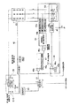
図16は従来の電力変換装置の一例を示す回路構成図である。図16において、商用電源1(50Hzまたは60HzのAC80〜260V)と液晶TVシステム2iとが設けられている。液晶TVシステム2iは、第1直流変換装置3’、第2直流変換装置4’、第3直流変換装置5’、放電管60a,60bを有するバックライト6、液晶ドライバ8、画像処理回路9、スピーカ10、リーケージ型トランスを有するDC−AC変換装置15からなる。
FIG. 16 is a circuit configuration diagram showing an example of a conventional power converter. In FIG. 16, a commercial power source 1 (50 Hz or 60 Hz AC 80 to 260 V) and a liquid crystal TV system 2 i are provided. The liquid crystal TV system 2i includes a
第1直流変換装置3’は、商用電源1からの交流電圧を直流電圧(例えばDC380V)に変換するとともに力率改善を行う。第2直流変換装置4’は、メイン電源であり、1次側と2次側とを絶縁し、第1直流変換装置3’の直流電圧を所定の直流電圧(例えばDC24V)に変換する。DC−AC変換装置15は、直流電圧を交流電圧(例えば65kHzのAC1500Vrms)に変換して、放電管60a,60bを点灯させる。
The first DC converter 3 'converts the AC voltage from the commercial power source 1 into a DC voltage (for example,
第2直流変換装置4’は、所定の直流電圧を液晶ドライバ8に供給して駆動させる。第3直流変換装置5’は、第1直流変換装置3’と画像処理回路9、スピーカ10間を電気的に絶縁し第1直流変換装置3’の直流電圧をDC12V,DC36Vに変換して画像処理回路9、スピーカ10に供給して駆動させる。
The second DC converter 4 ′ supplies and drives a predetermined DC voltage to the
このように、図16に示す電力変換装置によれば、商用電源1からの交流電力(電圧)を高電圧・高周波数の交流電力(電圧)に変換して、放電管60a,60bを発光させることができる。
As described above, according to the power conversion device shown in FIG. 16, the AC power (voltage) from the commercial power source 1 is converted into high voltage / high frequency AC power (voltage), and the
また、従来のこの種の技術としては、例えば特許文献1乃至特許文献4に記載されたものが知られている。
しかしながら、図16に示す電力変換装置にあっては、商用電源1から、最も負荷電力の大きい放電管60a,60bからなるバックライト6に電力を伝送するまでの間に、第1直流変換装置3’の電力変換、第2直流変換装置4’の電力変換、DC−AC変換装置15の電力変換の合計で3回の電力変換が行われている。
However, in the power conversion device shown in FIG. 16, the first
LCD−TVにおける消費電力の削減(省エネ化)には、光源自体の輝度効率の向上や各電力変換ブロックでの電力変換効率を高くするという方法もあるが、それらに加えて、最も電力を必要とする光源までの電力変換の回数を減らすことも効果的である。 In order to reduce power consumption (energy saving) in LCD-TV, there are methods of improving the luminance efficiency of the light source itself and increasing the power conversion efficiency in each power conversion block, but in addition to these methods, the most power is required. It is also effective to reduce the number of times of power conversion to the light source.
また、LEDは、直流電圧で点灯させることができるが、LEDの印加電圧(駆動電圧)は、そのIF−VF特性及び温度特性で決定される。このため、LEDの輝度を一定に制御する(電流を一定にする)場合、駆動電圧にはある程度の変動が発生するため、LEDの駆動電圧を他の負荷回路の入力電圧として直接、使用することは基本的にはできない。また、人が容易に手を触れることができるTVなどの家電装置の場合には、商用電源1とB/L(バックライト)6とは、安全のため、電気的に絶縁する必要がある。 The LED can be lit with a DC voltage, but the applied voltage (drive voltage) of the LED is determined by its IF-VF characteristics and temperature characteristics. For this reason, when the brightness of the LED is controlled to be constant (the current is constant), a certain amount of fluctuation occurs in the drive voltage, so the LED drive voltage should be used directly as an input voltage for other load circuits. Is basically not possible. Further, in the case of a household electric appliance such as a TV that can be easily touched by a person, the commercial power source 1 and the B / L (backlight) 6 need to be electrically insulated for safety.
例えば、図16に示す電力変換装置において、第2直流変換装置4’を削除して、第1直流変換装置3’の出力を、DC−AC変換装置15に直接入力する方法も考えられなくもないが、この場合、DC−AC変換装置15内の入出力の両方の電圧が高くなるリーケージ型トランスの部分で絶縁を行うことになるため、高価なトランスとなってしまうことと、該トランスからの大量の漏れ磁束に伴う、周辺PCB(プリント基板)の導体パターンでうず電流損失が発生したりするため、電力変換装置における1次側と2次側との絶縁を行う部分は、いずれかの直流変換装置で行う方がより理想的と言える。
For example, in the power conversion device shown in FIG. 16, a method of deleting the second DC conversion device 4 ′ and directly inputting the output of the first
本発明は、交流電源の交流電圧を直流電圧に変換し直流電圧で電気的に絶縁されたLED群負荷を駆動でき、交流電圧からLED群負荷までの電力変換の回数を減らすことで安価で高効率な電力変換装置を提供することにある。 The present invention is capable of driving an LED group load that is converted from an AC voltage of an AC power source into a DC voltage and electrically insulated by the DC voltage, and is inexpensive and high by reducing the number of times of power conversion from the AC voltage to the LED group load. An object is to provide an efficient power conversion device.
上記課題を解決するために、請求項1の発明は、交流電源からの交流電圧を直流電圧に変換するとともに力率改善を行う第1直流変換装置と、所定の直流電圧で発光するLED群負荷と、前記第1直流変換装置及び前記LED群負荷間を電気的に絶縁し且つ前記第1直流変換装置の直流電圧を前記所定の直流電圧に変換して前記LED群負荷に供給する第2直流変換装置とを備え、前記第2直流変換装置は、1次側と2次側とを絶縁するトランスと、前記トランスの2次側に配置され、前記LED群負荷に流れる電流を検出する電流検出回路と、前記電流検出回路で検出された検出電流値と電流基準値との誤差を増幅する誤差増幅器と、前記誤差増幅器の出力信号に基づく制御信号を前記1次側に伝達するための信号伝達絶縁素子と、前記1次側に配置され、前記信号伝達絶縁素子で伝達された制御信号に基づいてオン/オフすることにより前記トランスを介して前記2次側に電力を伝送するスイッチング素子とを備えることを特徴とする。 In order to solve the above-mentioned problems, the invention of claim 1 is directed to a first DC converter that converts an AC voltage from an AC power source into a DC voltage and improves the power factor, and an LED group load that emits light at a predetermined DC voltage. And a second DC that electrically insulates between the first DC converter and the LED group load, converts a DC voltage of the first DC converter to the predetermined DC voltage, and supplies the predetermined DC voltage to the LED group load. The second DC converter is disposed on the secondary side of the transformer and detects a current flowing through the LED group load. A circuit, an error amplifier for amplifying an error between a detected current value detected by the current detection circuit and a current reference value, and a signal transmission for transmitting a control signal based on an output signal of the error amplifier to the primary side An insulating element; Arranged on the side, characterized in that it comprises a switching device for transmitting power to the secondary side through the transformer by on / off based on a control signal transmitted by the signal transmitting insulating element.
請求項2の発明は、請求項1記載の電力変換装置において、前記第2直流変換装置は、前記トランスの2次側に、PWM調光信号により前記LED群負荷に電流を間欠的に流す時分割回路を備えることを特徴とする。 According to a second aspect of the present invention, there is provided the power converter according to the first aspect, wherein the second DC converter is configured to intermittently pass a current to the LED group load by a PWM dimming signal on the secondary side of the transformer. A division circuit is provided.
請求項3の発明は、請求項1又は2記載の電力変換装置において、前記第2直流変換装置は、前記トランスの1次側に、前記スイッチング素子をオン/オフ駆動する駆動回路を備えることを特徴とする。 According to a third aspect of the present invention, in the power converter according to the first or second aspect, the second DC converter includes a drive circuit that drives the switching element on / off on a primary side of the transformer. Features.
請求項4の発明は、請求項1乃至3のいずれか1項記載の電力変換装置において、前記第2直流変換装置は、前記トランスの1次側又は2次側に、前記スイッチング素子をオン/オフさせるパルス信号を生成するパルス変換回路を備えることを特徴とする。 According to a fourth aspect of the present invention, in the power conversion device according to any one of the first to third aspects, the second DC conversion device turns on / off the switching element on a primary side or a secondary side of the transformer. A pulse conversion circuit that generates a pulse signal to be turned off is provided.
請求項5の発明は、交流電源及びLED群負荷間を電気的に絶縁し且つ前記交流電源からの交流電圧を直流電圧に変換するとともに力率改善を行って前記LED群負荷に供給する第1直流変換装置を備え、前記第1直流変換装置は、1次側と2次側とを絶縁するトランスと、前記トランスの2次側に配置され、前記LED群負荷に流れる電流を検出する電流検出回路と、前記電流検出回路で検出された検出電流値と電流基準値との誤差を増幅する誤差増幅器と、前記誤差増幅器の出力信号に基づく制御信号を前記1次側に伝達するための信号伝達絶縁素子と、前記1次側に配置され、前記信号伝達絶縁素子で伝達された制御信号に基づいてオン/オフすることにより前記トランスを介して前記2次側に電力を伝送するスイッチング素子とを備えることを特徴とする。 According to a fifth aspect of the present invention, the AC power supply and the LED group load are electrically insulated from each other, the AC voltage from the AC power supply is converted into a DC voltage, and the power factor is improved to supply the first LED group load. The first DC converter includes a transformer that insulates the primary side from the secondary side, and a current detection that is disposed on the secondary side of the transformer and detects a current flowing through the LED group load. A circuit, an error amplifier for amplifying an error between a detected current value detected by the current detection circuit and a current reference value, and a signal transmission for transmitting a control signal based on an output signal of the error amplifier to the primary side An insulating element, and a switching element that is arranged on the primary side and transmits power to the secondary side through the transformer by turning on / off based on a control signal transmitted by the signal transmission insulating element Preparation And wherein the Rukoto.
請求項6の発明は、請求項5記載の電力変換装置において、前記第1直流変換装置は、前記トランスの2次側に配置され、PWM調光信号により前記LED群負荷に電流を間欠的に流す時分割回路を備えることを特徴とする。 According to a sixth aspect of the present invention, in the power conversion device according to the fifth aspect, the first DC conversion device is disposed on the secondary side of the transformer, and a current is intermittently supplied to the LED group load by a PWM dimming signal. A time-division circuit for flowing is provided.
請求項7の発明は、請求項5又は6記載の電力変換装置において、前記第1直流変換装置は、前記トランスの1次側に配置され、前記スイッチング素子をオン/オフ駆動する駆動回路を備えることを特徴とする。 According to a seventh aspect of the present invention, in the power conversion device according to the fifth or sixth aspect, the first DC conversion device includes a drive circuit that is disposed on a primary side of the transformer and that drives the switching element on / off. It is characterized by that.
請求項8の発明は、請求項5乃至7のいずれか1項記載の電力変換装置において、前記第1直流変換装置は、前記トランスの1次側又は2次側に、前記スイッチング素子をオン/オフさせるパルス信号を生成するパルス変換回路を備えることを特徴とする。 According to an eighth aspect of the present invention, in the power conversion device according to any one of the fifth to seventh aspects, the first DC conversion device turns on / off the switching element on a primary side or a secondary side of the transformer. A pulse conversion circuit that generates a pulse signal to be turned off is provided.
請求項9の発明は、交流電源及びLED群負荷間を電気的に絶縁し且つ前記交流電源の交流電圧を直流電圧に変換して前記LED群負荷に供給する第2直流変換装置を備え、前記第2直流変換装置は、1次側と2次側とを絶縁するトランスと、前記トランスの2次側に配置され、前記LED群負荷に流れる電流を検出する電流検出回路と、前記電流検出回路で検出された検出電流値と電流基準値との誤差を増幅する誤差増幅器と、前記誤差増幅器の出力信号に基づく制御信号を前記1次側に伝達するための信号伝達絶縁素子と、前記1次側に配置され、前記信号伝達絶縁素子で伝達された制御信号に基づいてオン/オフすることにより前記トランスを介して前記2次側に電力を伝送するスイッチング素子とを備えることを特徴とする。
The invention of
請求項10の発明は、請求項9記載の電力変換装置において、前記第2直流変換装置は、前記トランスの2次側に、PWM調光信号により前記LED群負荷に電流を間欠的に流す時分割回路を備えることを特徴とする。 According to a tenth aspect of the present invention, in the power converter according to the ninth aspect, the second DC converter is configured to intermittently pass a current to the LED group load by a PWM dimming signal on the secondary side of the transformer. A division circuit is provided.
請求項11の発明は、請求項9又は10記載の電力変換装置において、前記第2直流変換装置は、前記トランスの1次側に、前記スイッチング素子をオン/オフ駆動する駆動回路を備えることを特徴とする。 According to an eleventh aspect of the present invention, in the power converter according to the ninth or tenth aspect, the second DC converter includes a drive circuit for driving the switching element on / off on a primary side of the transformer. Features.
請求項12の発明は、請求項9乃至11のいずれか1項記載の電力変換装置において、前記第2直流変換装置は、前記トランスの1次側又は2次側に、前記スイッチング素子をオン/オフさせるパルス信号を生成するパルス変換回路を備えることを特徴とする。 According to a twelfth aspect of the present invention, in the power converter according to any one of the ninth to eleventh aspects, the second DC converter is configured to turn on / off the switching element on a primary side or a secondary side of the transformer. A pulse conversion circuit that generates a pulse signal to be turned off is provided.
本発明によれば、交流電源の交流電圧を直流電圧に変換し直流電圧で電気的に絶縁されたLED群負荷を駆動でき、交流電圧からLED群負荷までの電力変換の回数を減らすことで安価で高効率な電力変換装置を提供できる。 According to the present invention, it is possible to drive an LED group load which is converted from an AC voltage of an AC power source to a DC voltage and is electrically insulated by the DC voltage, and is inexpensive by reducing the number of times of power conversion from the AC voltage to the LED group load. Can provide a highly efficient power converter.
以下、本発明の電力変換装置の実施の形態を図面を参照しながら詳細に説明する。 Hereinafter, embodiments of a power conversion device of the present invention will be described in detail with reference to the drawings.
図1は本発明の実施例1の電力変換装置の回路構成図である。図1に示す電力変換装置は、商用電源(交流電源)1と液晶TVシステム2とを有する。液晶TVシステム2は、第1直流変換装置3、所定の直流電圧で発光する複数のLED(発光負荷)7a,7bを有するバックライト6、第2直流変換装置4、第3直流変換装置5を備える。
1 is a circuit configuration diagram of a power conversion device according to a first embodiment of the present invention. The power conversion apparatus shown in FIG. 1 has a commercial power supply (AC power supply) 1 and a liquid
第1直流変換装置3は、商用電源1からの交流電圧を直流電圧(例えばDC380V)に変換するとともに力率改善を行う。第2直流変換装置4は、メイン電源であり、第1直流変換装置3及びLED7a,7bを有するバックライト6間を電気的に絶縁し且つ第1直流変換装置3の直流電圧を所定の直流電圧に変換してLED7a,7bに供給して発光させる。
The
液晶ドライバ8、画像処理回路9、スピーカ10は、複数の負荷に相当し、液晶ドライバ8はDC24Vで駆動する。画像処理回路9はDC12Vで駆動する。スピーカ10はDC36Vで駆動する。
The
第3直流変換装置5は、サブ電源であり、第1直流変換装置3及び複数の負荷8〜10間を電気的に絶縁し第1直流変換装置3の直流電圧を複数の直流低電圧であるDC24V,DC12V,DC36Vに変換して液晶ドライバ8、画像処理回路9、スピーカ10に供給して各々を駆動させる。
The third DC converter 5 is a sub power source, and electrically insulates between the
なお、実施例1では、発光負荷として、複数のLEDから構成されるLED群負荷を用いているが、発光負荷は、直流電圧で発光するものであれば、例えばEL負荷であっても良い。あるいは、FED(フィールド・エミッション・ディスプレイ)負荷であっても良い。 In the first embodiment, an LED group load composed of a plurality of LEDs is used as the light emitting load. However, the light emitting load may be, for example, an EL load as long as it emits light with a DC voltage. Alternatively, it may be a FED (field emission display) load.
図2は本発明の実施例1の電力変換装置に設けられた第2直流変換装置の回路構成図である。図2に示す第2直流変換装置4は、1次巻線P1と2次巻線S1とにより1次側と2次側とを絶縁するトランスT1を含むフライバック方式コンバータからなる。なお、第2直流変換装置4は、1次側と2次側とを絶縁するトランスT1を含むフォワード方式コンバータを用いても良い。 FIG. 2 is a circuit configuration diagram of a second DC converter provided in the power converter according to Embodiment 1 of the present invention. 2 includes a flyback converter including a transformer T1 that insulates the primary side from the secondary side by the primary winding P1 and the secondary winding S1. The second DC converter 4 may use a forward converter that includes a transformer T1 that insulates the primary side from the secondary side.
第2直流変換装置4は、コンバータ回路20、制御回路部42およびゲート電圧設定抵抗R1を備えている。
The second DC converter 4 includes a
LED群負荷7は、図1における複数のLED7a,7bを有するバックライト6に相当し、直列に接続された複数のLEDからなるLED群が、並列に複数個(図2に示す例では「3」)接続されて構成されている。なお、並列に接続するLED群の数は任意である。このLED群負荷7は、コンバータ回路20の出力側と制御回路部42の内部のシンクドライバ50との間に接続されている。
The
コンバータ回路20は、制御回路部42から送られてくるPWM制御信号に応じた電圧を出力する。このコンバータ回路20からの出力電圧は、LED群負荷7のアノード側に印加される。
The
制御回路部42は、第1乃至第3電流検出回路44a〜44c、電流検出信号選択回路45、誤差増幅器46a、PWM制御コンパレータ46b、時分割回路46、ソフトスタート回路47および鋸波発生回路48a、ゲート電圧設定回路49、シンクドライバ50を備える。
The
時分割回路46は、トランスT1の2次側に配置され、外部から入力される直流のPWM調光信号に応じたデューティでオン/オフする時分割信号を生成する。具体的には、時分割回路46は、三角波発生回路48bとPWM調光コンパレータ(本発明のパルス変換回路)46cとを備える。三角波発生回路48bは、三角波信号を生成してPWM調光コンパレータ46cに送る。PWM調光コンパレータ46cは、外部から非反転入力端子(+)に入力されたPWM調光信号と、三角波発生回路48bから反転入力端子(−)に入力された三角波信号とを比較して、矩形波の時分割信号を生成する。この時分割回路46から出力される時分割信号は、ゲート電圧設定回路49に送られ、ゲート電圧設定回路49からシンクドライバ50へのゲート信号をオン/オフさせる。
The
ゲート電圧設定回路49は、時分割回路46から送られてくる時分割信号とゲート電圧設定抵抗R1で設定された電圧とに基づきゲート信号を生成し、ドライバ50に送る。
The gate
シンクドライバ50は、例えば複数(LED群の数と同数)のMOSFET(Q2〜Q4‥)から構成されており、そのゲートはゲート電圧設定回路49に接続され、ドレインはLED群負荷7のカソード側に接続され、ソースは接地されている。このシンクドライバ50に含まれるMOSFETは、時分割信号がオンの指示の期間中は、ゲート電圧設定回路49から送られてくるゲート信号に応じてオンすることにより、LED群負荷7に電流を流して発光させ、また、時分割信号がオフの指示の期間中は、ゲート電圧設定回路49から送られてくるゲート信号に応じてオフすることにより、LED群負荷7に流れる電流を停止させて発光を停止させる。
The
つまり、時分割信号のオン/オフのデューティー比に応じて、言い換えれば、外部から入力される直流のPWM調光信号に応じて、LED群負荷7の明るさを調整することができる。
That is, the brightness of the
尚、時分割信号がオンの指示の期間中のLED群負荷7に流れる3ラインの電流は、LEDのVFのばらつきなどによって、完全には同一にならない。
Note that the currents of the three lines flowing through the
第1乃至第3電流検出回路44a〜44cは、トランスT1の2次側に配置され、LED群負荷7からシンクドライバ50に流れる3ラインの電流を検出し、それぞれの電流に相当する電流検出信号を生成する。電流検出信号選択回路45は、LED群負荷7からシンクドライバ50に流れる3ラインの電流のそれぞれの電流に相当する3つの電流検出信号を入力して、そのうちの1つの電流検出信号を選択し、この選択した電流検出信号を誤差増幅器46aに送る。
The first to third
電流検出信号選択回路45での電流検出信号の選択方法は、入力された3つの電流検出信号のうちから、一番大きい信号を選択する方法になっていてもよいし、一番小さい信号を選択する方法になっていてもよい。
The method of selecting the current detection signal in the current detection
誤差増幅器46aは、トランスT1の2次側に配置され、電流検出信号選択回路45から送られてきて反転入力端子(−)に入力された電圧と非反転入力端子(+)に入力された基準値を表す電圧との誤差を増幅して、電流フィードバック信号としてPWM制御コンパレータ46bに送る。
The
ソフトスタート回路47は、制御回路42が動作を開始すると、電圧が低電圧(例えば0V)から徐々に上昇していくソフトスタート信号を生成し、PWM制御コンパレータ46bに送る。
When the
鋸波発生回路48aは、鋸波信号を発生し、PWM制御コンパレータ46bに送る。PWM制御コンパレータ46bは、誤差増幅器46aから送られてくる電流フィードバック信号、ソフトスタート回路47から送られてくるソフトスタート信号および鋸波発生回路48aから送られてくる鋸波信号に基づき矩形波のPWM制御信号を生成する。
The sawtooth
つまり、制御回路42の動作開始後のしばらくの期間は、PWM制御コンパレータ46bは、ソフトスタート回路47から送られてくるソフトスタート信号と、鋸波発生回路48aから送られてくる鋸波信号とを比較して、パルス幅が徐々に広くなるPWM制御信号を生成し、LED群負荷7が発光して、誤差増幅器46aから電流フィードバック信号が送られてくると、誤差増幅器46aから送られてくる電流フィードバック信号と、鋸波発生回路48aから送られてくる鋸波信号とを比較して、LED群負荷7に流れる電流に基づいたPWM制御信号を生成する。
That is, for a while after the operation of the
トランスT2(信号伝達絶縁素子)は、1次巻線P2と2次巻線S2とを有し、PWM制御信号を1次側の駆動回路43に送る。スイッチング素子Q1は、MOSFETからなり、第1直流変換装置3の出力に接続されたトランスT1の1次巻線P1に直列に接続されている。駆動回路43は、トランスT1の1次側に配置され、トランスT2により伝達されたPWM制御信号によりスイッチング素子Q1をオン/オフすることによりトランスT1を介して1次側から2次側に電力を伝送する。
The transformer T2 (signal transmission insulating element) has a primary winding P2 and a secondary winding S2, and sends a PWM control signal to the
ダイオードD1とコンデンサC1は、コンバータ回路20からの出力電圧を整流・平滑する整流平滑回路である。
The diode D1 and the capacitor C1 are a rectifying / smoothing circuit that rectifies and smoothes the output voltage from the
コンバータ回路20は、以上のような動作を行うことで、LED群負荷7を流れる電流に基づき該電流が所定電流になるようにスイッチング素子Q1のオン/オフを制御することで、LED群負荷7が必要とする電力を供給するとともに所定値に制御する。
The
図3は本発明の実施例1の電力変換装置に設けられた第1直流変換装置の回路構成図である。図3において、整流回路32は、ラインフィルタ31を介する商用電源1からの交流電圧を整流した整流電圧を出力する。PWM制御IC34によりスイッチング素子Q5がオンすると、整流電圧により、昇圧リアクトルL1→スイッチング素子Q5→グランドの経路で電流が流れて、昇圧リアクトルL1にエネルギーが蓄えられる。次に、スイッチング素子Q5がオフすると、昇圧リアクトルL1に蓄えられたエネルギーと整流電圧とがダイオードD2を介して平滑コンデンサC4に出力されるため、直流電圧に変換されるとともに昇圧される。
FIG. 3 is a circuit configuration diagram of a first DC converter provided in the power converter according to Embodiment 1 of the present invention. In FIG. 3, the
入力電圧検出回路33は、整流電圧を検出し、PWM制御IC34に出力する。出力電圧検出回路35は、平滑コンデンサC4における出力電圧を検出し、PWM制御IC34に出力する。PWM制御IC34は、検出された出力電圧に基づき該出力電圧が所定電圧になるようにスイッチング素子Q5のオン/オフを制御するとともに、スイッチング素子Q5を流れる電流のピークが入力電圧検出回路33で検出された整流電圧の波形と比例するように制御することで力率改善を行う。
The input
なお、図3は昇圧チョッパ回路の1種のDCM(電流不連続モード)と呼ばれる方式での例であるが、力率改善機能を有する回路であれば、CCM(電流連続モード)、インターリーブ方式、パッシブ型PFCでも、あるいはその他の直流変換装置でも良い。 FIG. 3 shows an example of a method called a DCM (current discontinuous mode) of the boost chopper circuit. However, if the circuit has a power factor correction function, CCM (current continuous mode), interleave method, A passive PFC or other DC converter may be used.
図4は本発明の実施例1の電力変換装置に設けられた第3直流変換装置の回路構成図である。図4に示す第3直流変換装置5は、1次巻線P3と2次巻線S3a,S3bとにより1次側と2次側とを絶縁するトランスT3を含むフォワード方式コンバータからなる。 FIG. 4 is a circuit configuration diagram of a third DC converter provided in the power converter of Embodiment 1 of the present invention. 4 includes a forward converter including a transformer T3 that insulates the primary side and the secondary side by the primary winding P3 and the secondary windings S3a and S3b.
図4において、入力側、即ち第1直流変換装置3の出力側には、MOSFETからなるスイッチング素子Q6とスイッチング素子Q7との直列回路が接続されている。スイッチング素子Q6とスイッチング素子Q7との接続点には、コンデンサC6とリアクトルL2とトランスT3の1次巻線P3との直列回路が接続されている。
In FIG. 4, a series circuit of a switching element Q6 and a switching element Q7 made of MOSFETs is connected to the input side, that is, the output side of the
この構成において、周波数制御IC51によりスイッチング素子Q7がオフしてスイッチング素子Q6がオンすると、1次側では、電源IN→Q6→C6→L2→P3の経路で電流が流れるため、2次側では、S3a→D3→C7の経路で電流が流れる。周波数制御IC51によりスイッチング素子Q6がオフしてスイッチング素子Q7がオンすると、1次側では、P3→L2→C6→Q7の経路で電流が流れるため、2次側では、S3b→D4→C7の経路で電流が流れる。
In this configuration, when the switching element Q7 is turned off and the switching element Q6 is turned on by the
出力電圧検出回路52は、コンデンサC7の出力電圧を検出し、フォトカプラ53を介して周波数制御IC51に出力する。周波数制御IC51は、コンデンサC7の出力電圧に基づき該出力電圧が所定電圧になるようにスイッチング素子Q6とスイッチング素子Q7とのオン/オフを制御する。
The output
第3直流変換装置5は、絶縁機能を有するものであれば、フライバック方式、共振型、その他の直流変換装置でも良い。 The third DC converter 5 may be a flyback method, a resonance type, or other DC converter as long as it has an insulating function.
このように、実施例1の電力変換装置によれば、商用電源1の交流電圧を第1直流変換装置3及び第2直流変換装置4により直流電圧に変換し、この直流電圧でLED7a,7bを発光でき、商用電源1からLED7a,7bまでの電力変換の回数を、従来の図16に示す回路に対して1回減らすことで安価で高効率な電力変換装置を提供できる。
Thus, according to the power converter of Example 1, the AC voltage of the commercial power source 1 is converted into a DC voltage by the
また、1次側と2次側との絶縁を行う部分は、第2直流変換装置4で行っており、DC−AC変換装置15で1次側と2次側との絶縁を行う場合のような無用なコストアップや効率低下をともなうこともない。
In addition, the part that insulates the primary side from the secondary side is performed by the second DC converter 4 and the DC-
図5は本発明の実施例2の電力変換装置の回路構成図である。図5に示す電力変換装置は、図1に示す実施例1の第3直流変換装置5を削除し、第2直流変換装置4の出力側に第4直流変換装置11を接続して、第4直流変換装置11の出力側に、液晶ドライバ8、画像処理回路9、スピーカ10を接続したことを特徴とする。
FIG. 5 is a circuit configuration diagram of the power conversion device according to the second embodiment of the present invention. The power converter shown in FIG. 5 deletes the 3rd DC converter 5 of Example 1 shown in FIG. 1, connects the
図6は本発明の実施例2の電力変換装置に設けられた第4直流変換装置の回路構成図である。図6に示す第4直流変換装置11において、第2直流変換装置4の出力側(IN)には、コンデンサC8の一端と抵抗R2の一端とトランジスタTr1のコレクタとが接続されている。抵抗R2の他端とトランジスタTr1のベースとツェナーダイオードZD1のカソードとが接続され、トランジスタTr1のエミッタは抵抗R101の一端とコンデンサC9の一端に接続され、抵抗R101の他端は抵抗R102の一端に接続され、抵抗R102の他端は抵抗R103の一端に接続され、コンデンサC8,C9の他端と抵抗R103の他端とツェナーダイオードZD1のアノードとは接地されている。
FIG. 6 is a circuit configuration diagram of a fourth DC converter provided in the power converter of
この構成によれば、トランジスタTr1のエミッタとコンデンサC9との接続点から直流電圧OUT1を得ることができ、抵抗R101と抵抗R102との接続点から直流電圧OUT2を得ることができ、抵抗R102と抵抗R103との接続点から直流電圧OUT3を得ることができる。 According to this configuration, the DC voltage OUT1 can be obtained from the connection point between the emitter of the transistor Tr1 and the capacitor C9, and the DC voltage OUT2 can be obtained from the connection point between the resistor R101 and the resistor R102. A DC voltage OUT3 can be obtained from the connection point with R103.
このような実施例2によっても、実施例1の効果と同様な効果が得られる。 According to the second embodiment, the same effect as that of the first embodiment can be obtained.
図7は本発明の実施例3の電力変換装置の回路構成図である。図7に示す電力変換装置は、図1に示す実施例1に対して、液晶ドライバ8を第3直流変換装置5aの出力側から切り離して第4直流変換装置11aの出力側に接続し、第4直流変換装置11aは、第2直流変換装置4の出力側の直流電圧を液晶ドライバ8を駆動するための直流低電圧に変換して液晶ドライバ8に供給することを特徴とする。
FIG. 7 is a circuit configuration diagram of the power conversion device according to the third embodiment of the present invention. The power converter shown in FIG. 7 is different from the first embodiment shown in FIG. 1 in that the
このような実施例3によっても、実施例1の効果と同様な効果が得られる。 According to the third embodiment, the same effect as that of the first embodiment can be obtained.
図8は本発明の実施例4の電力変換装置の回路構成図である。図8に示す電力変換装置は、商用電源(交流電源)1と液晶TVシステム2cとを有する。液晶TVシステム2cは、第1直流変換装置3a、複数のLED7a,7bを有するバックライト6、第3直流変換装置5b、液晶ドライバ8、画像処理回路9、スピーカ10を備える。
FIG. 8 is a circuit configuration diagram of the power conversion device according to the fourth embodiment of the present invention. The power converter shown in FIG. 8 has a commercial power supply (AC power supply) 1 and a liquid
第1直流変換装置3aは、商用電源1及びLED7a,7b間を電気的に絶縁し且つ商用電源1からの交流電圧を直流電圧(例えばDC380V)に変換するとともに力率改善を行って、LED7a,7bに供給して発光させる。
The
第3直流変換装置5bは、商用電源1及び複数の負荷8〜10間を電気的に絶縁し商用電源1の交流電圧を複数の直流低電圧であるDC24V,DC12V,DC36Vに変換して液晶ドライバ8、画像処理回路9、スピーカ10に供給して各々を駆動させる。
The
図9は本発明の実施例4の電力変換装置に設けられた第1直流変換装置の回路構成図である。図9に示す第1直流変換装置3aは、1次巻線P1と2次巻線S1と補助巻線P2,P3とにより1次側と2次側とを絶縁するトランスT1aを含むコンバータからなる。
FIG. 9 is a circuit configuration diagram of a first DC converter provided in the power converter of Embodiment 4 of the present invention. The
第1直流変換装置3aは、ラインフィルタ31、整流回路32、コンバータ回路20a、制御回路部42a及びゲート電圧設定抵抗R1を備えている。LED群負荷7は、図8における複数のLED(発光負荷)7a,7bを有するバックライト6に相当し、コンバータ回路20aの出力側と制御回路部42aの内部のシンクドライバ50との間に接続されている。
The
交流電圧がラインフィルタ31を介して整流回路32で整流されて、MOSFETからなるスイッチング素子Q8,Q9とトランスT1aとを含むコンバータ回路20aに送られる。
The AC voltage is rectified by the
コンバータ回路20aは、力率改善も兼ねた自励方式の2石式コンバータであり、スイッチング素子Q8とスイッチング素子Q9とは、交互にオン/オフを行う。また、コンバータ回路20aは、制御回路部42aから送られてくる電流フィードバック信号に基づいて、スイッチング素子Q9がオンしている期間(=オフするタイミング)を制御することで、LED負荷群7に必要とされる直流電圧を出力する。このコンバータ回路20aからの出力電圧は、LED群負荷7のアノード側に印加される。
The
制御回路部42aは、第1乃至第3電流検出回路44a〜44c、電流フィードバック信号選択回路45、誤差増幅器46a、時分割回路46、ゲート電圧設定回路49、シンクドライバ50を備える。
The
時分割回路46、ゲート電圧設定回路49、シンクドライバ50、第1乃至第3電流検出回路44a〜44c、電流フィードバック信号選択回路45は、図2に示すものと同一構成であるので、その説明は省略する。
The
誤差増幅器46aは、トランスT1の2次側に配置され、電流フィードバック信号選択回路45から送られてきて反転入力端子(−)に入力された電圧と非反転入力端子(+)に入力された基準値を表す電圧との誤差を増幅して、電流フィードバック信号としてフォトカプラPCのダイオードPCDに送る。
The
フォトカプラPCのダイオードPCDに、電流フィードバック信号に対応した電流が流れると、ダイオードPCDが発光し、フォトカプラPCのトランジスタPCTが受光する。即ち、フォトカプラPCにより電流フィードバックが1次側に送られる。この1次側に送られた電流フィードバックによりスイッチング素子Q9がオンしている期間(=オフするタイミング)を決定することでスイッチング素子Q8,Q9のオン/オフを制御を行うことにより、トランスT1aを介して1次側から2次側にLED負荷群7に必要とされる電力が伝送される。
When a current corresponding to the current feedback signal flows through the diode PCD of the photocoupler PC, the diode PCD emits light and the transistor PCT of the photocoupler PC receives light. That is, current feedback is sent to the primary side by the photocoupler PC. By controlling the on / off of the switching elements Q8 and Q9 by determining the period (= timing of turning off) of the switching element Q9 by the current feedback sent to the primary side, the transformer T1a Thus, electric power required for the
第1直流変換装置3は、絶縁機能と昇圧機能と力率改善機能とを有するものであれば、他励方式の2石式コンバータ(アクティブクランプ方式)、その他の直流変換装置でも良い。
As long as the
このように、実施例4の電力変換装置によれば、商用電源1の交流電圧を第1直流変換装置3aにより直流電圧に変換し、この直流電圧でLED7a,7bを発光でき、商用電源1からLED7a,7bまでの電力変換の回数を、従来の図16に示す回路に対して2回減らすことで更に安価で高効率な電力変換装置を提供できる。
Thus, according to the power converter of Example 4, the AC voltage of the commercial power source 1 is converted into a DC voltage by the
また、1次側と2次側との絶縁を行う部分は、第1直流変換装置3aで行っており、DC−AC変換装置15で1次側と2次側との絶縁を行う場合のような無用なコストアップや効率低下をともなうこともない。
In addition, the part that insulates the primary side from the secondary side is performed by the
図10は本発明の実施例5の電力変換装置の回路構成図である。図10に示す実施例5は、図8に示す実施例4の第3直流変換装置5を削除し、第1直流変換装置3aの出力側に第4直流変換装置11bを接続して、第4直流変換装置11bの出力側に、液晶ドライバ8、画像処理回路9、スピーカ10を接続したことを特徴とする。
FIG. 10 is a circuit configuration diagram of the power conversion device according to the fifth embodiment of the present invention. In the fifth embodiment shown in FIG. 10, the third DC converter 5 of the fourth embodiment shown in FIG. 8 is deleted, and the
このような実施例5によっても、実施例4の効果と同様な効果が得られる。 According to the fifth embodiment, the same effect as that of the fourth embodiment can be obtained.
図11は本発明の実施例6の電力変換装置の回路構成図である。図11に示す実施例6は、図8に示す実施例4に対して、液晶ドライバ8を第3直流変換装置5cの出力側から切り離して第4直流変換装置11cの出力側に接続し、第4直流変換装置11cは、第1直流変換装置3aの出力側の直流電圧を液晶ドライバ8を駆動するための直流低電圧に変換して液晶ドライバ8に供給することを特徴とする。
FIG. 11 is a circuit configuration diagram of the power conversion device according to the sixth embodiment of the present invention. The sixth embodiment shown in FIG. 11 is different from the fourth embodiment shown in FIG. 8 in that the
このような実施例6によっても、実施例4の効果と同様な効果が得られる。 According to the sixth embodiment, the same effect as that of the fourth embodiment can be obtained.
図12は本発明の実施例7の電力変換装置の回路構成図である。図12に示す電力変換装置は、商用電源(交流電源)1と液晶TVシステム2fとを有する。液晶TVシステム2fは、第2直流変換装置4a、複数のLED7a,7bを有するバックライト6、第3直流変換装置5b、液晶ドライバ8、画像処理回路9、スピーカ10を備える。
FIG. 12 is a circuit configuration diagram of the power conversion device according to the seventh embodiment of the present invention. The power conversion device shown in FIG. 12 includes a commercial power supply (AC power supply) 1 and a liquid
第2直流変換装置4aは、商用電源1及びLED7a,7b間を電気的に絶縁し且つ商用電源1の交流電圧を直流電圧に変換してLED7a,7bに供給して発光させる。
The
第3直流変換装置5bは、商用電源1及び複数の負荷8〜10間を電気的に絶縁し商用電源1の交流電圧を複数の直流低電圧であるDC24V,DC12V,DC36Vに変換して液晶ドライバ8、画像処理回路9、スピーカ10に供給して各負荷を駆動させる。
The
図13は本発明の実施例7の電力変換装置に設けられた第2直流変換装置の回路構成図である。図13に示す第2直流変換装置4aは、図2に示す実施例1の第2直流変換装置4に対して、入力側にラインフィルタ31、整流回路32を追加したことを特徴とし、その他の構成は同じである。
FIG. 13: is a circuit block diagram of the 2nd DC converter provided in the power converter device of Example 7 of this invention. The
このように、例えば、装置全体の総消費電力が75W以下であり、高調波対策が不要な場合などには、実施例7の電力変換装置のごとく、商用電源1の交流電圧を第2直流変換装置4aにより直流電圧に変換し、この直流電圧でLED7a,7bを発光でき、商用電源1からLED7a,7bまでの電力変換の回数を、減らすことで安価で高効率な電力変換装置を提供できる。
Thus, for example, when the total power consumption of the entire apparatus is 75 W or less and measures against harmonics are unnecessary, the AC voltage of the commercial power source 1 is converted into the second DC converter as in the power converter of the seventh embodiment. The
また、1次側と2次側との絶縁を行う部分は、第2直流変換装置4aで行っており、DC−AC変換装置15で1次側と2次側との絶縁を行う場合のような無用なコストアップや効率低下をともなうこともない。
In addition, the part that insulates the primary side from the secondary side is performed by the
図14は本発明の実施例8の電力変換装置の回路構成図である。図14に示す実施例8は、図12に示す実施例7の第3直流変換装置5bを削除し、第2直流変換装置4aの出力側に第4直流変換装置11dを接続して、第4直流変換装置11dの出力側に、液晶ドライバ8、画像処理回路9、スピーカ10を接続したことを特徴とする。
FIG. 14 is a circuit configuration diagram of the power conversion device according to the eighth embodiment of the present invention. In Example 8 shown in FIG. 14, the
このような実施例8によっても、実施例7の効果と同様な効果が得られる。 According to the eighth embodiment, the same effect as that of the seventh embodiment can be obtained.
図15は本発明の実施例9の電力変換装置の回路構成図である。図15に示す実施例9は、図12に示す実施例7に対して、液晶ドライバ8を第3直流変換装置5cの出力側から切り離して第4直流変換装置11eの出力側に接続し、第4直流変換装置11eは、第2直流変換装置4aの出力側の直流電圧を液晶ドライバ8を駆動するための直流低電圧に変換して液晶ドライバ8に供給することを特徴とする。
FIG. 15 is a circuit configuration diagram of the power conversion device according to the ninth embodiment of the present invention. The ninth embodiment shown in FIG. 15 is different from the seventh embodiment shown in FIG. 12 in that the
このような実施例9によっても、実施例7の効果と同様な効果が得られる。 According to the ninth embodiment, the same effect as that of the seventh embodiment can be obtained.
1 商用電源
2,2a〜2i 液晶TVシステム
3,3a 第1直流電源装置
4,4a 第2直流電源装置
5,5a〜5c 第3直流電源装置
6 バックライト
7 LED群負荷
7a,7b LED
8 液晶ドライバ
9 画像処理回路
10 スピーカ
11,11a〜11e 第4直流変換装置
20,20a コンバータ回路
31 ラインフィルタ
32 整流回路
42 制御回路部
43 駆動回路
44a 第1電流検出回路
44b 第2電流検出回路
44c 第3電流検出回路
45 電流検出信号選択回路
46 時分割回路
46a 誤差増幅器
46b PWM制御コンパレータ
47 ソフトスタート回路
48a 鋸波発生回路
49 ゲート電圧設定回路
50 シンクドライバ
T1,T2,T3,T1a トランス
R1 ゲート電圧設定抵抗
Q1,Q5,Q6,Q7,Q8,Q9 スイッチング素子
DESCRIPTION OF SYMBOLS 1
8
Claims (12)
所定の直流電圧で発光するLED群負荷と、
前記第1直流変換装置及び前記LED群負荷間を電気的に絶縁し且つ前記第1直流変換装置の直流電圧を前記所定の直流電圧に変換して前記LED群負荷に供給する第2直流変換装置とを備え、
前記第2直流変換装置は、
1次側と2次側とを絶縁するトランスと、
前記トランスの2次側に配置され、前記LED群負荷に流れる電流を検出する電流検出回路と、
前記電流検出回路で検出された検出電流値と電流基準値との誤差を増幅する誤差増幅器と、
前記誤差増幅器の出力信号に基づく制御信号を前記1次側に伝達するための信号伝達絶縁素子と、
前記1次側に配置され、前記信号伝達絶縁素子で伝達された制御信号に基づいてオン/オフすることにより前記トランスを介して前記2次側に電力を伝送するスイッチング素子と、
を備えることを特徴とする電力変換装置。 A first DC converter for converting an AC voltage from an AC power source into a DC voltage and improving the power factor;
LED group load that emits light at a predetermined DC voltage;
A second DC converter that electrically insulates between the first DC converter and the LED group load, converts a DC voltage of the first DC converter to the predetermined DC voltage, and supplies the predetermined DC voltage to the LED group load. And
The second DC converter is
A transformer that insulates the primary side from the secondary side;
A current detection circuit that is arranged on the secondary side of the transformer and detects a current flowing through the LED group load;
An error amplifier that amplifies an error between a detected current value detected by the current detection circuit and a current reference value;
A signal transmission insulating element for transmitting a control signal based on an output signal of the error amplifier to the primary side;
A switching element disposed on the primary side and transmitting power to the secondary side via the transformer by turning on / off based on a control signal transmitted by the signal transmission insulating element;
A power conversion device comprising:
前記第1直流変換装置は、
1次側と2次側とを絶縁するトランスと、
前記トランスの2次側に配置され、前記LED群負荷に流れる電流を検出する電流検出回路と、
前記電流検出回路で検出された検出電流値と電流基準値との誤差を増幅する誤差増幅器と、
前記誤差増幅器の出力信号に基づく制御信号を前記1次側に伝達するための信号伝達絶縁素子と、
前記1次側に配置され、前記信号伝達絶縁素子で伝達された制御信号に基づいてオン/オフすることにより前記トランスを介して前記2次側に電力を伝送するスイッチング素子と、
を備えることを特徴とする電力変換装置。 A first DC converter for electrically isolating the AC power supply and the LED group load and converting the AC voltage from the AC power source to a DC voltage and improving the power factor to supply the LED group load;
The first DC converter is
A transformer that insulates the primary side from the secondary side;
A current detection circuit that is arranged on the secondary side of the transformer and detects a current flowing through the LED group load;
An error amplifier that amplifies an error between a detected current value detected by the current detection circuit and a current reference value;
A signal transmission insulating element for transmitting a control signal based on an output signal of the error amplifier to the primary side;
A switching element disposed on the primary side and transmitting power to the secondary side via the transformer by turning on / off based on a control signal transmitted by the signal transmission insulating element;
A power conversion device comprising:
前記第2直流変換装置は、
1次側と2次側とを絶縁するトランスと、
前記トランスの2次側に配置され、前記LED群負荷に流れる電流を検出する電流検出回路と、
前記電流検出回路で検出された検出電流値と電流基準値との誤差を増幅する誤差増幅器と、
前記誤差増幅器の出力信号に基づく制御信号を前記1次側に伝達するための信号伝達絶縁素子と、
前記1次側に配置され、前記信号伝達絶縁素子で伝達された制御信号に基づいてオン/オフすることにより前記トランスを介して前記2次側に電力を伝送するスイッチング素子と、
を備えることを特徴とする電力変換装置。 A second DC converter that electrically insulates between the AC power source and the LED group load and converts the AC voltage of the AC power source into a DC voltage and supplies the converted voltage to the LED group load;
The second DC converter is
A transformer that insulates the primary side from the secondary side;
A current detection circuit that is arranged on the secondary side of the transformer and detects a current flowing through the LED group load;
An error amplifier that amplifies an error between a detected current value detected by the current detection circuit and a current reference value;
A signal transmission insulating element for transmitting a control signal based on an output signal of the error amplifier to the primary side;
A switching element disposed on the primary side and transmitting power to the secondary side via the transformer by turning on / off based on a control signal transmitted by the signal transmission insulating element;
A power conversion device comprising:
Priority Applications (4)
| Application Number | Priority Date | Filing Date | Title |
|---|---|---|---|
| JP2008192116A JP2010035271A (en) | 2008-07-25 | 2008-07-25 | Power converter |
| US12/507,304 US8054008B2 (en) | 2008-07-25 | 2009-07-22 | Power converter |
| US13/270,537 US8587220B2 (en) | 2008-07-25 | 2011-10-11 | Power converter |
| US14/034,195 US8847518B2 (en) | 2008-07-25 | 2013-09-23 | Power converter |
Applications Claiming Priority (1)
| Application Number | Priority Date | Filing Date | Title |
|---|---|---|---|
| JP2008192116A JP2010035271A (en) | 2008-07-25 | 2008-07-25 | Power converter |
Publications (1)
| Publication Number | Publication Date |
|---|---|
| JP2010035271A true JP2010035271A (en) | 2010-02-12 |
Family
ID=41568033
Family Applications (1)
| Application Number | Title | Priority Date | Filing Date |
|---|---|---|---|
| JP2008192116A Pending JP2010035271A (en) | 2008-07-25 | 2008-07-25 | Power converter |
Country Status (2)
| Country | Link |
|---|---|
| US (3) | US8054008B2 (en) |
| JP (1) | JP2010035271A (en) |
Cited By (2)
| Publication number | Priority date | Publication date | Assignee | Title |
|---|---|---|---|---|
| WO2011102449A1 (en) | 2010-02-19 | 2011-08-25 | 株式会社イノアックコーポレーション | Cushion pad and method for manufacturing same |
| JP2015211544A (en) * | 2014-04-25 | 2015-11-24 | ローム株式会社 | Power supply device, ac adapter, ac charger, electronic apparatus, and power supply system |
Families Citing this family (27)
| Publication number | Priority date | Publication date | Assignee | Title |
|---|---|---|---|---|
| WO2009064682A2 (en) | 2007-11-16 | 2009-05-22 | Allegro Microsystems, Inc. | Electronic circuits for driving series connected light emitting diode strings |
| KR101677730B1 (en) * | 2009-08-14 | 2016-11-30 | 페어차일드코리아반도체 주식회사 | LED light emitting device |
| TW201111931A (en) * | 2009-09-18 | 2011-04-01 | Starchips Technology Inc | Lighting apparatus and method for using the same |
| KR101569842B1 (en) | 2009-09-30 | 2015-11-17 | 삼성전자 주식회사 | A power supply unit for a television and a television including the same |
| KR101069960B1 (en) * | 2009-12-14 | 2011-10-04 | 삼성전기주식회사 | Initial driving circuit of backlight unit |
| CN102065600B (en) * | 2010-03-16 | 2014-06-25 | 成都芯源系统有限公司 | LED dimming driving system |
| TW201138553A (en) * | 2010-04-29 | 2011-11-01 | Green Solution Tech Co Ltd | Illumination controller and illumination driving system |
| CN101969723B (en) * | 2010-09-30 | 2013-06-26 | 杭州电子科技大学 | Non-light-coupled two-stage light-emitting diode (LED) driver circuit with high power factor |
| JP2013544011A (en) * | 2010-10-24 | 2013-12-09 | マイクロセミ コーポレィション | Synchronous control for LED string drivers |
| US9614452B2 (en) | 2010-10-24 | 2017-04-04 | Microsemi Corporation | LED driving arrangement with reduced current spike |
| US8692482B2 (en) | 2010-12-13 | 2014-04-08 | Allegro Microsystems, Llc | Circuitry to control a switching regulator |
| US8638045B2 (en) * | 2011-02-07 | 2014-01-28 | Cypress Semiconductor Corporation | Mutli-string LED current control system and method |
| CN102810299B (en) * | 2011-06-03 | 2015-06-03 | 乐金显示有限公司 | Backlight unit and method for driving the same |
| US9265104B2 (en) * | 2011-07-06 | 2016-02-16 | Allegro Microsystems, Llc | Electronic circuits and techniques for maintaining a consistent power delivered to a load |
| US9155156B2 (en) | 2011-07-06 | 2015-10-06 | Allegro Microsystems, Llc | Electronic circuits and techniques for improving a short duty cycle behavior of a DC-DC converter driving a load |
| CN102958221A (en) * | 2011-08-19 | 2013-03-06 | 台达电子企业管理(上海)有限公司 | Multichannel LED drive circuit |
| US8803437B2 (en) * | 2011-09-25 | 2014-08-12 | Wen-Hsiung Hsieh | Switching mode pulsed current supply for driving LEDS |
| US8575863B2 (en) * | 2011-11-08 | 2013-11-05 | Atmel Corporation | Color correcting device driver |
| US8604699B2 (en) | 2011-12-07 | 2013-12-10 | Atmel Corporation | Self-power for device driver |
| US8711119B2 (en) * | 2012-04-03 | 2014-04-29 | O2Micro, Inc. | Display systems with touch screens |
| US8810147B2 (en) * | 2012-07-15 | 2014-08-19 | Wen-Hsiung Hsieh | Method and circuit for driving LEDs with a pulsed current |
| US8716955B2 (en) * | 2012-07-26 | 2014-05-06 | Linkcom Manufacturing Co., Ltd. | Constant current LED driver |
| US9204504B2 (en) | 2012-09-17 | 2015-12-01 | Energy Focus, Inc. | LED lamp system |
| CN102938617A (en) * | 2012-10-31 | 2013-02-20 | 矽力杰半导体技术(杭州)有限公司 | Alternating current-direct current power converter |
| JP2014131391A (en) * | 2012-12-28 | 2014-07-10 | Sanken Electric Co Ltd | Dc power supply device |
| DE102013207327A1 (en) * | 2013-04-23 | 2014-10-23 | Tridonic Gmbh & Co. Kg | Converter module for the operation of lamps, with potential-separating clocked converter |
| EP3890445B1 (en) * | 2020-03-31 | 2025-12-10 | Tridonic GmbH & Co. KG | Primary side switched converter for providing a voltage supply to an led load |
Family Cites Families (21)
| Publication number | Priority date | Publication date | Assignee | Title |
|---|---|---|---|---|
| US5615093A (en) | 1994-08-05 | 1997-03-25 | Linfinity Microelectronics | Current synchronous zero voltage switching resonant topology |
| US5619402A (en) | 1996-04-16 | 1997-04-08 | O2 Micro, Inc. | Higher-efficiency cold-cathode fluorescent lamp power supply |
| US5930121A (en) | 1997-03-14 | 1999-07-27 | Linfinity Microelectronics | Direct drive backlight system |
| US6940733B2 (en) | 2002-08-22 | 2005-09-06 | Supertex, Inc. | Optimal control of wide conversion ratio switching converters |
| JP2005071681A (en) | 2003-08-21 | 2005-03-17 | Sumida Corporation | High pressure transformer and discharge lamp driving circuit using the same |
| JP5025913B2 (en) | 2005-05-13 | 2012-09-12 | シャープ株式会社 | LED drive circuit, LED illumination device, and backlight |
| JP4535385B2 (en) * | 2005-08-01 | 2010-09-01 | 株式会社小糸製作所 | Lighting control device for vehicle lamp |
| JP2007080771A (en) * | 2005-09-16 | 2007-03-29 | Nec Lighting Ltd | Low voltage power supply circuit for lighting, lighting device, and low voltage power supply output method for lighting |
| TW200812438A (en) | 2006-08-30 | 2008-03-01 | Nat Univ Chung Cheng | Ripple-free drive circuit for LED backlights of LCD panel |
| TWI382384B (en) | 2006-10-25 | 2013-01-11 | Gigno Technology Co Ltd | Inverter and driving device of backlight module |
| US7554473B2 (en) * | 2007-05-02 | 2009-06-30 | Cirrus Logic, Inc. | Control system using a nonlinear delta-sigma modulator with nonlinear process modeling |
| US7579786B2 (en) | 2007-06-04 | 2009-08-25 | Applied Concepts, Inc. | Method, apparatus, and system for driving LED's |
| JP4799493B2 (en) * | 2007-06-29 | 2011-10-26 | 株式会社小糸製作所 | Vehicle lighting |
| TW200921597A (en) | 2007-11-08 | 2009-05-16 | Chunghwa Picture Tubes Ltd | Display device and driving voltage compensation device for backlight module |
| US7855520B2 (en) * | 2008-03-19 | 2010-12-21 | Niko Semiconductor Co., Ltd. | Light-emitting diode driving circuit and secondary side controller for controlling the same |
| US8314572B2 (en) | 2008-06-24 | 2012-11-20 | Atmel Corporation | Apparatus and methodology for enhancing efficiency of a power distribution system having power factor correction capability by using a self-calibrating controller |
| JP2010035270A (en) | 2008-07-25 | 2010-02-12 | Sanken Electric Co Ltd | Power conversion apparatus |
| JP5600456B2 (en) * | 2009-05-19 | 2014-10-01 | ローム株式会社 | Light emitting diode drive circuit, light emitting device and display device using the same, and drive circuit protection method |
| KR101275399B1 (en) * | 2010-12-13 | 2013-06-17 | 삼성전기주식회사 | Light emitting diodes driver |
| CN102340911B (en) * | 2010-12-30 | 2013-08-07 | 矽力杰半导体技术(杭州)有限公司 | Control circuit and control method for light emitting diode (LED) driver |
| KR101057684B1 (en) * | 2011-03-31 | 2011-08-18 | 주식회사 동운아나텍 | Lighting drive |
-
2008
- 2008-07-25 JP JP2008192116A patent/JP2010035271A/en active Pending
-
2009
- 2009-07-22 US US12/507,304 patent/US8054008B2/en active Active
-
2011
- 2011-10-11 US US13/270,537 patent/US8587220B2/en not_active Expired - Fee Related
-
2013
- 2013-09-23 US US14/034,195 patent/US8847518B2/en active Active
Cited By (2)
| Publication number | Priority date | Publication date | Assignee | Title |
|---|---|---|---|---|
| WO2011102449A1 (en) | 2010-02-19 | 2011-08-25 | 株式会社イノアックコーポレーション | Cushion pad and method for manufacturing same |
| JP2015211544A (en) * | 2014-04-25 | 2015-11-24 | ローム株式会社 | Power supply device, ac adapter, ac charger, electronic apparatus, and power supply system |
Also Published As
| Publication number | Publication date |
|---|---|
| US8847518B2 (en) | 2014-09-30 |
| US20120025725A1 (en) | 2012-02-02 |
| US8054008B2 (en) | 2011-11-08 |
| US20100019696A1 (en) | 2010-01-28 |
| US8587220B2 (en) | 2013-11-19 |
| US20140021876A1 (en) | 2014-01-23 |
Similar Documents
| Publication | Publication Date | Title |
|---|---|---|
| JP2010035271A (en) | Power converter | |
| JP2010035270A (en) | Power conversion apparatus | |
| US8749171B2 (en) | Lighting apparatus and control method thereof | |
| JP4934508B2 (en) | LCD backlight drive system with LED | |
| US9215769B2 (en) | LED backlight driver system and associated method of operation | |
| US9485819B2 (en) | Single stage LED driver system, control circuit and associated control method | |
| US20120248998A1 (en) | Led driver and led illuminator having the same | |
| US20080018261A1 (en) | LED power supply with options for dimming | |
| US20110227493A1 (en) | Light emitting diode driver systems and associated methods of control | |
| WO2005112245A1 (en) | Power supply device and display device | |
| TW201301936A (en) | A cascade boost and inverting buck converter with independent control | |
| JP2008009416A (en) | Driving system of liquid crystal display backlight with light emitting diode | |
| CN106464126A (en) | Initial-Side Controlled LED Driver with Ripple Cancellation | |
| KR20100014323A (en) | A cell arrangement for feeding electrical loads such as light sources, corresponding circuit and design method | |
| KR20150001033A (en) | Power supplying apparatus | |
| KR20110132188A (en) | LED driving device with improved power factor | |
| KR20120031215A (en) | Led driving device for lighting | |
| JP2013116003A (en) | Lighting device | |
| KR101496819B1 (en) | Single stage forward-flyback converter, power supplying apparatus and power suppying apparatus for light emitting diode | |
| Chansri et al. | A high power LED driver with Class D ZVS series resonant converter | |
| CN104935165A (en) | power supply | |
| KR101130292B1 (en) | LED driving device for backlight of the LCD | |
| JP2012195251A (en) | Led drive circuit | |
| CN102374448B (en) | lighting device | |
| US8674612B2 (en) | Fluorescent tube driving device |