JP2009512213A - Simoth image sensor wafer level package using silicon via contact and method of manufacturing the same - Google Patents
Simoth image sensor wafer level package using silicon via contact and method of manufacturing the same Download PDFInfo
- Publication number
- JP2009512213A JP2009512213A JP2008535426A JP2008535426A JP2009512213A JP 2009512213 A JP2009512213 A JP 2009512213A JP 2008535426 A JP2008535426 A JP 2008535426A JP 2008535426 A JP2008535426 A JP 2008535426A JP 2009512213 A JP2009512213 A JP 2009512213A
- Authority
- JP
- Japan
- Prior art keywords
- substrate
- image sensor
- wafer level
- via hole
- forming
- Prior art date
- Legal status (The legal status is an assumption and is not a legal conclusion. Google has not performed a legal analysis and makes no representation as to the accuracy of the status listed.)
- Pending
Links
Images


Classifications
-
- H—ELECTRICITY
- H10—SEMICONDUCTOR DEVICES; ELECTRIC SOLID-STATE DEVICES NOT OTHERWISE PROVIDED FOR
- H10F—INORGANIC SEMICONDUCTOR DEVICES SENSITIVE TO INFRARED RADIATION, LIGHT, ELECTROMAGNETIC RADIATION OF SHORTER WAVELENGTH OR CORPUSCULAR RADIATION
- H10F39/00—Integrated devices, or assemblies of multiple devices, comprising at least one element covered by group H10F30/00, e.g. radiation detectors comprising photodiode arrays
- H10F39/80—Constructional details of image sensors
- H10F39/804—Containers or encapsulations
-
- H10W72/20—
Landscapes
- Solid State Image Pick-Up Elements (AREA)
Abstract
【課題】シリコン・バイア・コンタクトを利用したシーモス・イメージ・センサーのウェハー・レべル・パッケージおよびその方法を提供する。
【解決手段】シーモス・イメージ・センサーのウェハー・レべル・パッケージは、複数の電極パッドを含むイメージ・センサーの構成要素が形成された基板と、基板の上部面に取り付けられる透明基板と、基板の下部面から上部面の複数の電極パッドの下面にわたり形成されたバイア・ホールと、バイア・ホール内の電極パッド下面を除く残りの部分及び基板の裏面全体に形成された保護膜と、バイア・ホール内に形成されたバイア・コンタクトと、基板の裏面のバイア・コンタクト上に形成されたソルダー・バンプとで構成される。
【選択図】図15A wafer level package of a Simoth image sensor using a silicon via contact and a method thereof are provided.
A wafer level package of a Simoth image sensor includes a substrate on which image sensor components including a plurality of electrode pads are formed, a transparent substrate attached to an upper surface of the substrate, and a substrate. A via hole formed from the lower surface of the substrate to the lower surface of the plurality of electrode pads on the upper surface, a protective film formed on the remaining portion of the via hole except the lower surface of the electrode pad and the entire back surface of the substrate, A via contact formed in the hole and a solder bump formed on the via contact on the back surface of the substrate.
[Selection] Figure 15
Description
本発明は、シーモス・イメージ・センサーのウェハー・レべル・パッケージおよびその製造方法に関する。 The present invention relates to a wafer level package for a Simoth image sensor and a method for manufacturing the same.
より詳しくは、センシング部および電極パッドを含むイメージ・センサー構成要素が形成された上部面と、上部面に対向された下部面として電極パッドを直接連結するシリコン・バイア・コンタクトを形成して下部面に露出したシリコン・バイア・コンタクトにソルダー・バンプを形成し、PCB(Printed Circuit Board)と接着するシリコン・バイア・コンタクトを利用したシーモス・イメージ・センサーのウェハー・レべル・パッケージおよびその方法に関する。 More specifically, an upper surface on which an image sensor component including a sensing unit and an electrode pad is formed and a silicon via contact that directly connects the electrode pad as a lower surface facing the upper surface to form a lower surface. A wafer level package for a Simoth image sensor using a silicon via contact that forms a solder bump on a silicon via contact exposed on the surface and adheres to a PCB (Printed Circuit Board) and a method thereof .
一般的に、イメージ・センサーは、光学映像を電気的信号に変換させる半導体モジュールとして、映像信号を保存、送信およびディスプレー装置として表わすために使う。イメージ・センサーは、電位の井戸(Potential well)の深さを電位を伝達しようとする方向に連続的に調節し、電荷を送る電荷結合素子(Charge−CouPled Device、以下CCD)イメージ・センサーと、ーつのピクセル単位のセル(Ce11)の内部にーつ以上のトランジスクと、光センサーとして動作するフオト・ダイオードとからなるシーモス(CMOS)イメージ・センサーに大きく分類される。 In general, an image sensor is used as a semiconductor module that converts an optical image into an electrical signal to store, transmit, and represent the image signal as a display device. The image sensor is a charge-coupled device (CCD) image sensor that continuously adjusts the depth of a potential well in a direction in which the potential is transmitted and transmits a charge. It is broadly classified into a CMOS image sensor composed of one or more transistors inside a pixel unit cell (Ce11) and a photodiode operating as a photosensor.
CCDイメージ・センサーは、CM0Sイメージ・センサーに比ペて、ノイズが少なく、イメージ品質が優秀であり、デジタル・カメラに適合している。これに反してCMOSイメージ・センサーは、おおむねCCDイメージ・センサーに比べて生産単価と消費電力が低く、周辺回路のチップと統合しやすいという長所がある。特に、CM0Sイメージ・センサーは、一般的な半導体製造技術として生産することができ、増幅および信号処理のような機能を遂行する周辺システムとの統合がしやすく、生産原価を低<することが可能である。さらに、処理速度が速く、CCDイメージ・センサーに比べて1%程度消費電力が小さいことが特徴である。したがって、CMOSイメージ・センサーは、携帯電話と個人携帯端末機(PDA)用カメラに利用することに適合していたが、最近CMOSイメージ・センサー技術の進歩によりCCDとCMOSイメージ・センサー間の境界が崩れている。 The CCD image sensor has less noise than the CM0S image sensor, has excellent image quality, and is suitable for a digital camera. On the other hand, the CMOS image sensor has advantages in that the unit price and power consumption are generally lower than those of the CCD image sensor, and it is easy to integrate with the chip of the peripheral circuit. In particular, the CM0S image sensor can be produced as a general semiconductor manufacturing technology, can be easily integrated with peripheral systems that perform functions such as amplification and signal processing, and can reduce production costs. It is. Furthermore, the processing speed is fast and the power consumption is about 1% smaller than that of the CCD image sensor. Therefore, CMOS image sensors have been adapted for use in mobile phones and personal digital assistant (PDA) cameras, but recently, advances in CMOS image sensor technology have led to the boundary between CCD and CMOS image sensors. It has collapsed.
即ち、CMOSイメージ・センサーは、当初VGA級のカメラフォン用のイメージ・センサーとして利用されてきたが、最近の技術発展によって2Maga画素程度のカメラ・フォン用のイメージ・センサーとして採用される等その技術開発速度が非常に早<なっている。 In other words, the CMOS image sensor was originally used as an image sensor for a VGA-class camera phone, but it has been adopted as an image sensor for a camera phone with about 2 Mega pixels due to recent technological development. Development speed is very fast.
ところで、今までは、イメージ・センサー・チップのためのパッケージを利用して、ワイヤー・ボンディング(Wire Bonding)によってモジュール化が進行している。しかし、ワイヤー・ボンディング工程によると、センサーの窓(ウインドウ)に画像欠陥を起こす異質物が発生し、モジュール組み立ての際、収率を減少させる間題が発生し、モジュールの厚さと横、縦サイズが大きくなってモジュールの小型化が困難である。 By the way, until now, modularization has progressed by wire bonding using a package for an image sensor chip. However, according to the wire bonding process, foreign objects that cause image defects are generated in the sensor window, and the problem of reducing the yield occurs during the assembly of the module. It becomes difficult to reduce the size of the module.
最近の新しいカメラ・モジュール化方法として、LCD(Liquid Crystal DISplay)パネル製造技術において使われた異方性伝導フィルム(ACF:Anisotropic Conductive Film)を活用したCOF(Chip on Flexible PCB)技術が活用初期段階にある。大韓民国公開特許第2003−0069321号明細書は、基板状態においてパッケージング工程を終わらせるフリップ・チップ(Flip Chip)Auバンピング工程とCOF実装技術を使った撮像素子パッケージおよびその製造方法を開示している。 COF (Chip on Flexible PCB) technology that utilizes anisotropic conductive film (ACF) used in LCD (Liquid Crystal Display) panel manufacturing technology is an early stage of utilization as a new camera modularization method. It is in. Korean Patent Application Publication No. 2003-0069321 discloses an image pickup device package using a flip chip Au bumping process and COF mounting technology that ends the packaging process in a substrate state, and a manufacturing method thereof. .
図1は、従来技術にともなうCIS(CMOS Image Sensor)チップを使ったカメラ・モジュールを示した図面である。 FIG. 1 shows a camera module using a CIS (CMOS Image Sensor) chip according to the prior art.
また、図1に図示されたように、ClSチップ(105)上に形成されたソルダー・バンプ(Solder BumP、120b)を異方性伝導フィルム(104)の伝導性ボールを通じて、フレキシブル回路基板(Flexible Printed Circuit Board、以下FPC、103)の外部電極パッド(120a)と連結してCISチップのポンディングを完了する。以後、レンズ(100)、レンズ・ハウジング(101)および赤外線フィルター(図示していない)等を装着することによって、カメラ・モジュールを完成する。このように異方性伝導フィルム技術を活用することによって、CISのための別途のパッケージが必要なく、CIS(105)チップを直接FPC(103)に接合できる。 Further, as shown in FIG. 1, a solder bump (Solder Bump, 120b) formed on a ClS chip (105) is passed through a conductive ball of an anisotropic conductive film (104) to form a flexible circuit board (Flexible). It is connected to the external electrode pad (120a) of the Printed Circuit Board (hereinafter FPC, 103) to complete the bonding of the CIS chip. Thereafter, the camera module is completed by mounting the lens (100), the lens housing (101), the infrared filter (not shown), and the like. By utilizing the anisotropic conductive film technology as described above, a CIS (105) chip can be directly bonded to the FPC (103) without requiring a separate package for CIS.
しかし、前記のようなフリップ・チップ方式は、イメージ・センシングをするためのセンシング部(106)が必然的に前記異方性伝導フィルム(104)に向かわなければならないので、前記CISチップ(105)をFPC(103)に接合する際、異方性伝導フィルム(104)等から発生した汚染物質が、CISチップのセンシング部(106)に入り、製造工程上の収率を大きく低下させる問題点がある。 However, in the flip chip method as described above, since the sensing unit (106) for performing image sensing must be directed to the anisotropic conductive film (104), the CIS chip (105) is required. When joining the FPC (103) to the FPC (103), contaminants generated from the anisotropic conductive film (104) and the like enter the sensing part (106) of the CIS chip, which greatly reduces the yield in the manufacturing process. is there.
このような問題を解決するために、イスラエルのShellcase社では、基板を食刻し、前記基板のセンシング部と同じ平面上に形成された電極パッドに連結する電極を基板裏面(センシング部の反対面)に延長してCISチップのセンシング部を異方性伝導フィルムの反対側へ向かうようにして、FPCと接合できる技術を開発した。 In order to solve such a problem, Shellcase Inc., Israel, etches a substrate and connects an electrode connected to an electrode pad formed on the same plane as the sensing portion of the substrate to the back surface of the substrate (the opposite surface of the sensing portion). ) And developed a technology that can be joined to the FPC by extending the sensing part of the CIS chip to the opposite side of the anisotropic conductive film.
図2乃至図6は、Shellcase社のCISパッケージ製造工程に対する断面図である。 2 to 6 are cross-sectional views for the CIS package manufacturing process of Shellcase.
まず、図2に示されたように、所定の工程を経て、基板(200)の第1面(200a)に電極パッド(201)と撮像のためのセンシング部(202)等のCIS構成成分を形成する。以下において記述するイメージ・センサー・パッケージ製造工程完了の後、切断面(250)に沿って切断することによってチップとチップを分離することになる。 First, as shown in FIG. 2, through a predetermined process, CIS components such as an electrode pad (201) and a sensing unit (202) for imaging are formed on the first surface (200a) of the substrate (200). Form. After completion of the image sensor package manufacturing process described below, the chips are separated by cutting along the cutting plane (250).
次に、図3に示されたように、前記基板(200)の第1面にエポキシ(epoxy、203)を使って第1ガラス基板(204)を付着する。 Next, as shown in FIG. 3, a first glass substrate (204) is attached to the first surface of the substrate (200) using an epoxy (203).
次に、図4に示されたように、前記基板(200)の第1面に存在する電極パッド(201)が露出するまで、前記基板を第2面(2O0b)から円(206)の中に図示されたように食刻(206)した後、エポキシ(203a)を利用して第2ガラス基板(207)を付着する。 Next, as shown in FIG. 4, the substrate is removed from the second surface (2O0b) into the circle (206) until the electrode pad (201) present on the first surface of the substrate (200) is exposed. After etching (206), the second glass substrate (207) is attached using epoxy (203a).
次に、図5に示されたように、前記第2ガラス基板(207)を食刻した後、導電体を形成してパターニングし、外部電極(208)を形成する。前記外部電極(208)は、前記電極パッド(201)とティー接合(T−contact、209)を形成する。 Next, as shown in FIG. 5, after etching the second glass substrate (207), a conductor is formed and patterned to form an external electrode (208). The external electrode (208) forms a tee junction (T-contact, 209) with the electrode pad (201).
次に、図6に図示されたように、前記第2ガラス基板(207)と前記外部電極(208)上に絶縁膜(211)を蒸着し、パターニングして、ソルダー・バンプが形成される領域を露出させた後、ソルダー・バンプ(210)を形成して、前記基板(200)を切断面(250)に沿って切断することによって、チップとチップの間を分離する。その後、 所定の工程を経て、カメラのような映像装置モジュールとして組み立てが成される。 Next, as shown in FIG. 6, an insulating film (211) is deposited on the second glass substrate (207) and the external electrode (208) and patterned to form solder bumps. Then, a solder bump (210) is formed, and the substrate (200) is cut along the cutting surface (250) to separate the chips from each other. After that, through a predetermined process, an assembly is made as a video device module such as a camera.
しかし、前記のようなイメージ・センサー・パッケージ製造方法は、前記テイー接合する部位において導電体の亀裂およぴその亀裂による停電が発生しやすい。また、外部電極を形成するためのパターニング工程もしなければなれず、外部電極を保護用またはソルダー・マスク用の絶縁膜を形成しなければならないなど、製造工程が複雑であり、収率が低い問題がある。 However, the image sensor package manufacturing method as described above is liable to cause a crack in the conductor and a power failure due to the crack at the portion where the tee is joined. In addition, the patterning process for forming the external electrode must be performed, and the manufacturing process is complicated and the yield is low. For example, the external electrode must be formed with an insulating film for protection or solder mask. There is.
したがって、本発明の目的は、前記のような従来技術の問題点を解決するためのものであり、イメージ・センシング部に異質物が入ることを防止するものである。 Accordingly, an object of the present invention is to solve the above-described problems of the prior art, and to prevent foreign substances from entering the image sensing unit.
また、本発明の他の目的は、イメージ・センサー・モジュールの厚さを減少させたイメージ・センサー・パッケージを提供することにある。 Another object of the present invention is to provide an image sensor package in which the thickness of the image sensor module is reduced.
本願の第1発明によるイメージ・センサーのパッケージング方法は、
複数の電極パッドを含むイメージ・センサーの構成要素が形成された基板の上部面に透明基板を付着する段階と、
前記基板の下部面を研磨し、基板の不要部分を除去する段階と、
前記基板の下部面から前記基板の上部面の複数の電極パッドの下まで貫くバイア・ホールを形成する段階と、
前記バイア・ホール内部および前記基板の下部面全体に保護膜を形成する段階と、
前記電極パッド上に形成された保護膜を除去し、前記バイア・ホール内にシード層を形成する段階と、
金属で前記バイア・ホールを充填することで、前記バイア・ホール上にバイア・コンタクトを形成する段階と、
前記基板下部面の前記バイア・コンタクト上にソルダー・バンプを形成する段階と、
前記基板および透明基板を切断して分離する段階とから構成される。
The image sensor packaging method according to the first invention of the present application is as follows:
Attaching a transparent substrate to the upper surface of the substrate on which image sensor components including a plurality of electrode pads are formed;
Polishing the lower surface of the substrate and removing unnecessary portions of the substrate;
Forming via holes penetrating from a lower surface of the substrate to a plurality of electrode pads on an upper surface of the substrate;
Forming a protective film inside the via hole and on the entire lower surface of the substrate;
Removing a protective film formed on the electrode pad and forming a seed layer in the via hole;
Forming a via contact on the via hole by filling the via hole with metal; and
Forming solder bumps on the via contacts on the bottom surface of the substrate;
And cutting and separating the substrate and the transparent substrate.
また、本願の第2発明のイメージ・センサーのパッケージは、
複数の電極パッドを含むイメージ・センサーの構成要素が形成された基板と、
前記基板の上部面に付着した透明基板と、
前記基板の下部面から前記基板の上部面の複数の電極パッド下部まで形成されたバイア・ホールと、
前記バイア・ホール内部の前記電極パッド下部面を除いた残り部分と前記基板の下部面全体に形成された保護膜と、
前記バイア・ホール内部に形成されたバイア・コンタクトと、
前記基板の下部面の前記バイア・コンタクト上に形成されたソルダー・バンプと、
で構成したものである。
The image sensor package of the second invention of the present application is:
A substrate on which image sensor components including a plurality of electrode pads are formed;
A transparent substrate attached to the upper surface of the substrate;
Via holes formed from the lower surface of the substrate to the lower portions of the plurality of electrode pads on the upper surface of the substrate;
A protective film formed on the remaining portion of the via hole except the lower surface of the electrode pad and the entire lower surface of the substrate;
Via contacts formed inside the via holes;
Solder bumps formed on the via contacts on the lower surface of the substrate;
It is composed of
本発明の前記目的と技術的構成およびそれにともなう作用効果に関する詳しい事項は、以下において詳細に説明される。 Detailed matters concerning the above-mentioned object and technical configuration of the present invention and the operation and effect associated therewith will be described in detail below.
図7乃至図16は、本発明の一実施例にともなうシリコン・バイア・コンタクトを利用したシーモス・イメージ・センサーのウェハー・レべル・パッケージング方法の断面図である。 7 to 16 are cross-sectional views illustrating a wafer level packaging method for a Simoth image sensor using a silicon via contact according to an embodiment of the present invention.
図7に示されたように、基板(300)は、上部に所定の工程を経て、外部回路との電気的接続のための電極パッド(301)とイメージ・センシングのためのセンシング部(302)が形成されている。前記基板(300)は、多数のチップとして構成されており、チップ製造工程完了後に、パッケージングのために、チップ間を切断するという工程を遂行する。前記切断工程のための切断面(303)を基準として、チップとチップの間を分離することになる。前記基板(300)はシリコン基板、すなわちウェハー(wafer)である。
As shown in FIG. 7, the substrate (300) is subjected to a predetermined process on the electrode pad (301) for electrical connection with an external circuit and a sensing unit (302) for image sensing. Is formed. The
次に、図8に図示されたように、前記基板(300)の上部に透明基板(304)を付着する。前記透明基板(304)は、ガラス基盤(glass substrate)にすることが好ましく、厚さは300−500μmが好ましい。前記透明基板(304)を付着させるために、切断面(303)を基準として両側の電極パッド(301)にわたるようエポキシ層(epoxy layer、305)を形成する。また、前記透明基板(304)と基板(300)の間に空間を設けるために、スペイサー(spacer、306)を前記エポキシ層(305)上部に形成する。その後、前記基板(300)と前記透明基板(304)を接着する。これによって、今後の工程において、基板(300)の上部に形成されたセンシング部(302)および電極パッド(301)は、外部の不純物から完壁に保護され、不純物による不良率を画期的に減少することができる。
Next, as shown in FIG. 8, a transparent substrate (304) is attached on top of the substrate (300). The
次に、図9に示されたように、前記基板(300)の下段部を研磨する。前記研磨する工程は、今後、基板(300)にバイア・ホールを形成する過程において、工程を容易にするために、堅固性(Durability)を考慮し、クラインディング後の前記基板(300)の厚さを、50−100μmとすることが好ましい。 Next, as shown in FIG. 9, the lower part of the substrate (300) is polished. In the process of forming a via hole in the substrate (300) in the future, the polishing process is performed in consideration of the durability and the thickness of the substrate (300) after the grinding in order to facilitate the process. The thickness is preferably 50-100 μm.
次に、図10に示されたように、前記基板(300)の下部から上部に形成された電極パッド(301)の下部まで貫くバイア・ホールを(307)を形成する。前記バイアホールを(307)を形成する方法は、RIE(Reactive Ion Etching)を利用した乾式食刻で直接形成したり、部分的な未貫通ホールを形成した後、前記基板(300)の貫通されなかった残り部分を乾式食刻または湿式食刻として除去し、形成することができる。この際、バイア・ホールの直径は、数μmから数千μmまでが可能であるが、200μm以内において形成することが好ましい。前記バイア・ホール(307)の形状は、円形を基本とするものの三角形、四角形または多角形のように多様な形状が可能である。また、前記基板(300)の下部に形成された貫通ホールの断面積が、前記電極パッド(301)側の断面積より大きい場合と、小さい場合、または同じである場合ある。
Next, as shown in FIG. 10, via holes (307) are formed through the substrate (300) from the bottom to the bottom of the electrode pad (301) formed at the top. The via
次に、図11に示されたように、前記バイア・ホール(307)の内部および基板(300)の下部面の全体にかけて、電極間の絶縁のために保護膜(Passivation layer、308)を形成する。前記保護膜(308)は、酸化膜または窒化膜として形成されることが好ましい。前記保護膜(308)は、低温PECVD(Low−Temparature Plasma enhanced Chemical Vapor Deposition、 PECVD)で蒸着することが好ましい。
Next, as shown in FIG. 11, a passivation layer (308) is formed in the via hole (307) and the entire lower surface of the substrate (300) for insulation between the electrodes. To do. The
次に、図12に示されたように、バイア・ホール(307)内部の電極パッド(301)の露出のために、バイア・ホール(307)底面部、すなわち電極パッド領域に蒸着されている保護膜(308)を除去する。 Next, as shown in FIG. 12, for the exposure of the electrode pad (301) inside the via hole (307), the protection deposited on the bottom surface of the via hole (307), that is, the electrode pad region. The film (308) is removed.
次に、図13と図14に示されたように、バイア・ホール(307)内部にスパッタリング工程で、シード層(seed layer、309)を形成した後、半田ペーストを印刷又は鍍金によって、バイア・コンタクト(Via Contact、310)を形成する。この際、使われる金属は、伝導性物質すなわち、Au、Ag、Cu、Al、Ni、CrおよびW、又はこれらの合金のような導電性金属であれば何であっても使用可能である。 Next, as shown in FIGS. 13 and 14, after forming a seed layer (seed layer 309) in a via hole (307) by a sputtering process, a solder paste is printed or plated to form a via layer. A contact (Via Contact, 310) is formed. In this case, any metal may be used as long as it is a conductive material, that is, a conductive metal such as Au, Ag, Cu, Al, Ni, Cr and W, or an alloy thereof.
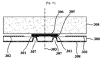
次に、図15に示されたように、基板(300)の下部面のバイア・コンタクト(310)が形成された領域に、ソルダー・バンプ(Soldar Bump、311)を形成する。前記ソルダー・バンプは、導電性物質であれば何であっても可能であるが、Cu、Au、Ni/Auの合金、Sn/Auの合金などが好ましい。 Next, as shown in FIG. 15, solder bumps (Soldar Bumps, 311) are formed on the lower surface of the substrate (300) where the via contacts (310) are formed. The solder bump may be any conductive material, but Cu, Au, Ni / Au alloy, Sn / Au alloy, and the like are preferable.
最後に、図16に図示されたように、基板(300)および透明基板(304)を切断面(303)に沿って切断(dicing)し、チップとチップの間を分離する。 Finally, as shown in FIG. 16, the substrate (300) and the transparent substrate (304) are diced along the cutting plane (303) to separate the chips.
詳述した本発明の実施例の過程を通じて、イメージ・センサー・チップが完成される。その後、前記分離したイメージ・センサーチップは、基板下部に生成されたソルダー・バンプを通じてFPCまたは印刷回路基板に付着させることによって、外部回路と接続することになる。以後、レンズおよびレンズ・ハウジングなどを組み立てて、カメラのような映像装置を構成する。 Through the process of the embodiment of the present invention described in detail, the image sensor chip is completed. Thereafter, the separated image sensor chip is connected to an external circuit by being attached to an FPC or a printed circuit board through solder bumps generated at the bottom of the substrate. Thereafter, an image device such as a camera is constructed by assembling a lens and a lens housing.
本発明は、好ましい実施例をあげて図示し説明しているが、前記の実施例に限らず、多くの変形が、本発明の技術的思想内において、当分野の通常の知識を持つものにより可能であることは明白である。 Although the present invention has been illustrated and described with reference to the preferred embodiments, the present invention is not limited to the above-described embodiments, and many modifications will be apparent to those skilled in the art within the technical idea of the present invention. Obviously it is possible.
したがって、本発明によると、センシング部および電極パッドを含むイメージ・センサー構成要素が形成された基板の上部面に、基板の下部面から電極パッドまで連結するバイア・コンタクトを簡単に形成することができる。また、基板下部面に露出されたバイア・コンタクト上にソルダー・バンプを形成した後、イメージ・センサー構成要素のない下部面を通じて、外部回路と連結することによって、各種の汚染物がセンシング部に引入されて発生するパッケージング工程の際の収率低下を防ぐことができる。 Therefore, according to the present invention, a via contact connecting from the lower surface of the substrate to the electrode pad can be easily formed on the upper surface of the substrate on which the image sensor component including the sensing unit and the electrode pad is formed. . In addition, after forming solder bumps on the via contacts exposed on the lower surface of the board, various contaminants enter the sensing unit by connecting to external circuits through the lower surface without the image sensor components. Thus, it is possible to prevent the yield from being reduced during the packaging process.
また、基板の厚さの不必要な部分を除去することによって、完成されたイメージ・センサー・モジュールの厚さを減らすことができる。 Also, the thickness of the completed image sensor module can be reduced by removing unnecessary portions of the substrate thickness.
また、徐々に小型化されているイメージ・センサーを含む半導体素子のCSP(ChiP Sca1e Package)を効果的に具現することもでき、さらに、MCM(Multi Chip Module)等に応用することも可能である。 Further, it is possible to effectively implement a CSP (ChiP Scale Package) of a semiconductor element including an image sensor that is gradually reduced in size, and to be applied to an MCM (Multi Chip Module) and the like. .
Claims (16)
複数の電極パッドを含むイメージ・センサーの構成要素が形成された基板の上部面に透明基板を付着する段階と、
前記基板の下部面を研磨する段階と、
前記基板の下部面から前記基板の上部面の複数の電極パッドの下まで貫くバイア・ホールを形成する段階と、
前記バイア・ホール内部および前記基板の下部面全体に保護膜を形成する段階と、
前記電極パッド上に形成された保護膜を除去し、前記バイア・ホール内にシード層を形成する段階と、
前記シード層上にバイア・コンタクトを形成する段階と、
前記基板下部面の前記バイア・コンタクト上にソルダー・バンプを形成する段階と、
前記基板および透明基板を切断して分離する段階と、
からなることを特徴とするシーモス・イメージ・センサーのウェハー・レべル・パッケージング方法。 In the image sensor packaging method,
Attaching a transparent substrate to the upper surface of the substrate on which image sensor components including a plurality of electrode pads are formed;
Polishing the lower surface of the substrate;
Forming via holes penetrating from a lower surface of the substrate to a plurality of electrode pads on an upper surface of the substrate;
Forming a protective film inside the via hole and on the entire lower surface of the substrate;
Removing a protective film formed on the electrode pad and forming a seed layer in the via hole;
Forming a via contact on the seed layer;
Forming solder bumps on the via contacts on the bottom surface of the substrate;
Cutting and separating the substrate and the transparent substrate;
A wafer level packaging method for a Simoth image sensor, comprising:
前記エポキシ層の上部にスペイサーを形成する段階と、
をさらに含むことを特徴とする請求項1に記載のシーモス・イメージ・センサーのウェハーレペル・パッケージング方法。 Before attaching the transparent substrate to the upper surface of the substrate, forming an epoxy layer over the electrode pads on both sides with respect to the cut surface;
Forming a spacer on top of the epoxy layer;
The wafer repel packaging method of a sea moss image sensor according to claim 1, further comprising:
前記バイア・ホール内部にスパッタリングにより前記シード層を形成する段階と、
半田ペーストを印刷することにより、又は、前記バイア・ホール内の金属層上に金属を鍍金することで、前記バイア・ホールを金属で充填する段階と、
をさらに含むことを特徴とする請求項1に記載のシーモス・イメージ・センサーのウェハー・レべル・パッケージング方法。 Via contact formation in the via hole is as follows:
Forming the seed layer by sputtering inside the via hole;
Filling the via hole with metal by printing a solder paste or by plating metal on the metal layer in the via hole;
The wafer level packaging method of the sea moss image sensor according to claim 1, further comprising:
複数の電極パッドを含むイメージ・センサーの構成要素が形成された基板と、
前記基板の上部面に付着した透明基板と、
乾式食刻または湿式食刻により、前記基板の下部面から前記基板の上部面の複数の電極パッド下部まで形成されたバイア・ホールと、
前記バイア・ホール内部の前記電極パッド下部面を除いた残り部分と前記基板の下部面全体に形成された保護膜と、
前記バイア・ホール内部に形成されたシード層及びバイア・コンタクトと、
前記基板の下部面の前記バイア・コンタクト上に形成されたソルダー・バンプと、
で構成したことを特徴とするシーモス・イメージ・センサーのウェハー・レべル・パッケージ。 In the image sensor package,
A substrate on which image sensor components including a plurality of electrode pads are formed;
A transparent substrate attached to the upper surface of the substrate;
Via holes formed from the lower surface of the substrate to the lower portions of the plurality of electrode pads on the upper surface of the substrate by dry etching or wet etching,
A protective film formed on the remaining portion of the via hole except the lower surface of the electrode pad and the entire lower surface of the substrate;
A seed layer and a via contact formed inside the via hole;
Solder bumps formed on the via contacts on the lower surface of the substrate;
The wafer level package of Simoth Image Sensor, which is characterized by comprising
Applications Claiming Priority (1)
| Application Number | Priority Date | Filing Date | Title |
|---|---|---|---|
| PCT/KR2005/003370 WO2007043718A1 (en) | 2005-10-11 | 2005-10-11 | Wafer level package using silicon via contacts for cmos image sensor and method of fabricating the same |
Publications (1)
| Publication Number | Publication Date |
|---|---|
| JP2009512213A true JP2009512213A (en) | 2009-03-19 |
Family
ID=37942929
Family Applications (1)
| Application Number | Title | Priority Date | Filing Date |
|---|---|---|---|
| JP2008535426A Pending JP2009512213A (en) | 2005-10-11 | 2005-10-11 | Simoth image sensor wafer level package using silicon via contact and method of manufacturing the same |
Country Status (3)
| Country | Link |
|---|---|
| US (1) | US20080217715A1 (en) |
| JP (1) | JP2009512213A (en) |
| WO (1) | WO2007043718A1 (en) |
Families Citing this family (28)
| Publication number | Priority date | Publication date | Assignee | Title |
|---|---|---|---|---|
| US7091124B2 (en) | 2003-11-13 | 2006-08-15 | Micron Technology, Inc. | Methods for forming vias in microelectronic devices, and methods for packaging microelectronic devices |
| US8084866B2 (en) | 2003-12-10 | 2011-12-27 | Micron Technology, Inc. | Microelectronic devices and methods for filling vias in microelectronic devices |
| US20050247894A1 (en) | 2004-05-05 | 2005-11-10 | Watkins Charles M | Systems and methods for forming apertures in microfeature workpieces |
| US7232754B2 (en) | 2004-06-29 | 2007-06-19 | Micron Technology, Inc. | Microelectronic devices and methods for forming interconnects in microelectronic devices |
| US7425499B2 (en) | 2004-08-24 | 2008-09-16 | Micron Technology, Inc. | Methods for forming interconnects in vias and microelectronic workpieces including such interconnects |
| US7083425B2 (en) | 2004-08-27 | 2006-08-01 | Micron Technology, Inc. | Slanted vias for electrical circuits on circuit boards and other substrates |
| US7300857B2 (en) | 2004-09-02 | 2007-11-27 | Micron Technology, Inc. | Through-wafer interconnects for photoimager and memory wafers |
| US7271482B2 (en) | 2004-12-30 | 2007-09-18 | Micron Technology, Inc. | Methods for forming interconnects in microelectronic workpieces and microelectronic workpieces formed using such methods |
| US7795134B2 (en) | 2005-06-28 | 2010-09-14 | Micron Technology, Inc. | Conductive interconnect structures and formation methods using supercritical fluids |
| US7262134B2 (en) | 2005-09-01 | 2007-08-28 | Micron Technology, Inc. | Microfeature workpieces and methods for forming interconnects in microfeature workpieces |
| US7863187B2 (en) | 2005-09-01 | 2011-01-04 | Micron Technology, Inc. | Microfeature workpieces and methods for forming interconnects in microfeature workpieces |
| US7622377B2 (en) | 2005-09-01 | 2009-11-24 | Micron Technology, Inc. | Microfeature workpiece substrates having through-substrate vias, and associated methods of formation |
| US7749899B2 (en) | 2006-06-01 | 2010-07-06 | Micron Technology, Inc. | Microelectronic workpieces and methods and systems for forming interconnects in microelectronic workpieces |
| US7629249B2 (en) | 2006-08-28 | 2009-12-08 | Micron Technology, Inc. | Microfeature workpieces having conductive interconnect structures formed by chemically reactive processes, and associated systems and methods |
| US7902643B2 (en) | 2006-08-31 | 2011-03-08 | Micron Technology, Inc. | Microfeature workpieces having interconnects and conductive backplanes, and associated systems and methods |
| SG150410A1 (en) | 2007-08-31 | 2009-03-30 | Micron Technology Inc | Partitioned through-layer via and associated systems and methods |
| US7884015B2 (en) | 2007-12-06 | 2011-02-08 | Micron Technology, Inc. | Methods for forming interconnects in microelectronic workpieces and microelectronic workpieces formed using such methods |
| GB2463866A (en) * | 2008-09-24 | 2010-03-31 | Wai Hung Chan | High-speed CMOS image sensors |
| US8355628B2 (en) * | 2009-03-06 | 2013-01-15 | Visera Technologies Company Limited | Compact camera module |
| US9190388B2 (en) * | 2011-12-19 | 2015-11-17 | Intel Corporation | Using an optically transparent solid material as a support structure for attachment of a semiconductor material to a substrate |
| KR101401988B1 (en) * | 2012-09-07 | 2014-05-30 | 주식회사 동부하이텍 | Semiconductor package and semiconductor package forming scheme |
| CN102881644B (en) * | 2012-10-12 | 2014-09-03 | 江阴长电先进封装有限公司 | Method for packaging wafer level chip |
| US20140326856A1 (en) * | 2013-05-06 | 2014-11-06 | Omnivision Technologies, Inc. | Integrated circuit stack with low profile contacts |
| CN103400807B (en) * | 2013-08-23 | 2016-08-24 | 苏州晶方半导体科技股份有限公司 | The wafer level packaging structure of image sensor and method for packing |
| WO2015157124A1 (en) * | 2014-04-07 | 2015-10-15 | Flir Systems, Inc. | Method and systems for coupling semiconductor substrates |
| US10103191B2 (en) | 2017-01-16 | 2018-10-16 | Semiconductor Components Industries, Llc | Semiconductor die and method of packaging multi-die with image sensor |
| KR102492733B1 (en) | 2017-09-29 | 2023-01-27 | 삼성디스플레이 주식회사 | Copper plasma etching method and manufacturing method of display panel |
| TWI685125B (en) * | 2018-12-05 | 2020-02-11 | 海華科技股份有限公司 | Image capturing module and portable electronic device |
Citations (3)
| Publication number | Priority date | Publication date | Assignee | Title |
|---|---|---|---|---|
| JP2004055674A (en) * | 2002-07-17 | 2004-02-19 | Fuji Photo Film Co Ltd | Semiconductor device and manufacturing method thereof |
| JP2005051080A (en) * | 2003-07-29 | 2005-02-24 | Hamamatsu Photonics Kk | Backside incident photodetector and its manufacturing method |
| WO2005022631A1 (en) * | 2003-08-28 | 2005-03-10 | Fujikura Ltd. | Semiconductor package and manufacturing method thereof |
Family Cites Families (7)
| Publication number | Priority date | Publication date | Assignee | Title |
|---|---|---|---|---|
| US20030049925A1 (en) * | 2001-09-10 | 2003-03-13 | Layman Paul Arthur | High-density inter-die interconnect structure |
| JP4000507B2 (en) * | 2001-10-04 | 2007-10-31 | ソニー株式会社 | Method for manufacturing solid-state imaging device |
| TWI229435B (en) * | 2002-06-18 | 2005-03-11 | Sanyo Electric Co | Manufacture of semiconductor device |
| JP4443865B2 (en) * | 2002-06-24 | 2010-03-31 | 富士フイルム株式会社 | Solid-state imaging device and manufacturing method thereof |
| JP5030360B2 (en) * | 2002-12-25 | 2012-09-19 | オリンパス株式会社 | Method for manufacturing solid-state imaging device |
| JP4544876B2 (en) * | 2003-02-25 | 2010-09-15 | 三洋電機株式会社 | Manufacturing method of semiconductor device |
| KR100526191B1 (en) * | 2003-06-18 | 2005-11-03 | 삼성전자주식회사 | Solid-State Imaging Apparatus |
-
2005
- 2005-10-11 JP JP2008535426A patent/JP2009512213A/en active Pending
- 2005-10-11 US US12/088,529 patent/US20080217715A1/en not_active Abandoned
- 2005-10-11 WO PCT/KR2005/003370 patent/WO2007043718A1/en not_active Ceased
Patent Citations (3)
| Publication number | Priority date | Publication date | Assignee | Title |
|---|---|---|---|---|
| JP2004055674A (en) * | 2002-07-17 | 2004-02-19 | Fuji Photo Film Co Ltd | Semiconductor device and manufacturing method thereof |
| JP2005051080A (en) * | 2003-07-29 | 2005-02-24 | Hamamatsu Photonics Kk | Backside incident photodetector and its manufacturing method |
| WO2005022631A1 (en) * | 2003-08-28 | 2005-03-10 | Fujikura Ltd. | Semiconductor package and manufacturing method thereof |
Also Published As
| Publication number | Publication date |
|---|---|
| WO2007043718A1 (en) | 2007-04-19 |
| US20080217715A1 (en) | 2008-09-11 |
Similar Documents
| Publication | Publication Date | Title |
|---|---|---|
| JP2009512213A (en) | Simoth image sensor wafer level package using silicon via contact and method of manufacturing the same | |
| KR100608420B1 (en) | Image sensor chip package and manufacturing method thereof | |
| KR101032182B1 (en) | Semiconductor Packages and Camera Modules | |
| US8309398B2 (en) | Electronic device wafer level scale packages and fabrication methods thereof | |
| US7948555B2 (en) | Camera module and electronic apparatus having the same | |
| KR100616670B1 (en) | Wafer-level image sensor module and its manufacturing method | |
| KR20190117444A (en) | Semiconductor device and method of manufacturing semiconductor device | |
| US20080055438A1 (en) | Image sensor package, related method of manufacture and image sensor module | |
| US20090050995A1 (en) | Electronic device wafer level scale packges and fabrication methods thereof | |
| JP4660259B2 (en) | Manufacturing method of semiconductor device | |
| WO2008143461A2 (en) | Wafer level chip scale package of an image sensor by means of through hole interconnection and method for manufacturing the same | |
| KR100572487B1 (en) | Image sensor package and manufacturing method | |
| JP4641820B2 (en) | Manufacturing method of semiconductor device | |
| CN101356645A (en) | Method for encapsulating and manufacturing CMOS image sensor wafer using silicium through-hole contact point | |
| TW200841460A (en) | Wafer level package using silicon via contacts for CMOS image sensor and method of fabricating the same | |
| KR101020876B1 (en) | Wafer Level Chip Scale Package and Fabrication Method of Semiconductor Device by Through Hole Interconnect | |
| KR100682238B1 (en) | Manufacturing method of semiconductor chip module | |
| CN101101918A (en) | Semiconductor device and its making method | |
| CN100446229C (en) | Semiconductor device and manufacturing method thereof | |
| KR100715858B1 (en) | Method for manufacturing wafer level package with patterned conductive adhesive and image sensor module (ISM) using the same | |
| KR100897761B1 (en) | Wafer Level Package of Silicon Image Sensor Using Through Via Hole Process and Its Manufacturing Method | |
| KR100640336B1 (en) | Image sensor assembly | |
| KR20090098497A (en) | Wafer Level Chip Size Package of Integrated Device Using Dicing Process and Manufacturing Method Thereof |
Legal Events
| Date | Code | Title | Description |
|---|---|---|---|
| A977 | Report on retrieval |
Free format text: JAPANESE INTERMEDIATE CODE: A971007 Effective date: 20111114 |
|
| A131 | Notification of reasons for refusal |
Free format text: JAPANESE INTERMEDIATE CODE: A131 Effective date: 20111122 |
|
| A02 | Decision of refusal |
Free format text: JAPANESE INTERMEDIATE CODE: A02 Effective date: 20120424 |