JP2009236493A - Flaw inspecting method of transparent plate and flaw inspection device - Google Patents
Flaw inspecting method of transparent plate and flaw inspection device Download PDFInfo
- Publication number
- JP2009236493A JP2009236493A JP2008079068A JP2008079068A JP2009236493A JP 2009236493 A JP2009236493 A JP 2009236493A JP 2008079068 A JP2008079068 A JP 2008079068A JP 2008079068 A JP2008079068 A JP 2008079068A JP 2009236493 A JP2009236493 A JP 2009236493A
- Authority
- JP
- Japan
- Prior art keywords
- light
- transparent plate
- subject
- inspection
- light amount
- Prior art date
- Legal status (The legal status is an assumption and is not a legal conclusion. Google has not performed a legal analysis and makes no representation as to the accuracy of the status listed.)
- Pending
Links
- 238000007689 inspection Methods 0.000 title claims abstract description 99
- 238000000034 method Methods 0.000 title claims abstract description 59
- 230000007547 defect Effects 0.000 claims abstract description 113
- 238000009826 distribution Methods 0.000 claims abstract description 92
- 238000012937 correction Methods 0.000 claims abstract description 57
- 230000000873 masking effect Effects 0.000 claims abstract description 34
- 230000003287 optical effect Effects 0.000 claims abstract description 29
- 238000005259 measurement Methods 0.000 claims description 61
- 238000003384 imaging method Methods 0.000 claims description 52
- 230000008569 process Effects 0.000 claims description 20
- 238000012545 processing Methods 0.000 claims description 15
- 238000001514 detection method Methods 0.000 abstract description 13
- 230000002950 deficient Effects 0.000 description 13
- NIXOWILDQLNWCW-UHFFFAOYSA-M Acrylate Chemical compound [O-]C(=O)C=C NIXOWILDQLNWCW-UHFFFAOYSA-M 0.000 description 12
- 239000004973 liquid crystal related substance Substances 0.000 description 7
- 230000009467 reduction Effects 0.000 description 7
- 239000011347 resin Substances 0.000 description 6
- 229920005989 resin Polymers 0.000 description 6
- -1 2-ethylhexyl Chemical group 0.000 description 5
- 230000007423 decrease Effects 0.000 description 5
- 239000000113 methacrylic resin Substances 0.000 description 5
- 230000004048 modification Effects 0.000 description 5
- 238000012986 modification Methods 0.000 description 5
- VVQNEPGJFQJSBK-UHFFFAOYSA-N Methyl methacrylate Chemical group COC(=O)C(C)=C VVQNEPGJFQJSBK-UHFFFAOYSA-N 0.000 description 4
- 230000007246 mechanism Effects 0.000 description 4
- 239000000178 monomer Substances 0.000 description 4
- 230000035945 sensitivity Effects 0.000 description 4
- 239000007787 solid Substances 0.000 description 4
- 230000000007 visual effect Effects 0.000 description 4
- LYCAIKOWRPUZTN-UHFFFAOYSA-N Ethylene glycol Chemical compound OCCO LYCAIKOWRPUZTN-UHFFFAOYSA-N 0.000 description 3
- 230000008859 change Effects 0.000 description 3
- 229920001577 copolymer Polymers 0.000 description 3
- 238000004519 manufacturing process Methods 0.000 description 3
- 238000002834 transmittance Methods 0.000 description 3
- BAPJBEWLBFYGME-UHFFFAOYSA-N Methyl acrylate Chemical compound COC(=O)C=C BAPJBEWLBFYGME-UHFFFAOYSA-N 0.000 description 2
- 229920000297 Rayon Polymers 0.000 description 2
- PPBRXRYQALVLMV-UHFFFAOYSA-N Styrene Chemical compound C=CC1=CC=CC=C1 PPBRXRYQALVLMV-UHFFFAOYSA-N 0.000 description 2
- NIXOWILDQLNWCW-UHFFFAOYSA-N acrylic acid group Chemical group C(C=C)(=O)O NIXOWILDQLNWCW-UHFFFAOYSA-N 0.000 description 2
- 230000031700 light absorption Effects 0.000 description 2
- 239000002344 surface layer Substances 0.000 description 2
- 150000003923 2,5-pyrrolediones Chemical class 0.000 description 1
- 125000000954 2-hydroxyethyl group Chemical group [H]C([*])([H])C([H])([H])O[H] 0.000 description 1
- 125000003903 2-propenyl group Chemical group [H]C([*])([H])C([H])=C([H])[H] 0.000 description 1
- UJTRCPVECIHPBG-UHFFFAOYSA-N 3-cyclohexylpyrrole-2,5-dione Chemical compound O=C1NC(=O)C(C2CCCCC2)=C1 UJTRCPVECIHPBG-UHFFFAOYSA-N 0.000 description 1
- FWEOQOXTVHGIFQ-UHFFFAOYSA-N 8-anilinonaphthalene-1-sulfonic acid Chemical compound C=12C(S(=O)(=O)O)=CC=CC2=CC=CC=1NC1=CC=CC=C1 FWEOQOXTVHGIFQ-UHFFFAOYSA-N 0.000 description 1
- CERQOIWHTDAKMF-UHFFFAOYSA-M Methacrylate Chemical compound CC(=C)C([O-])=O CERQOIWHTDAKMF-UHFFFAOYSA-M 0.000 description 1
- CERQOIWHTDAKMF-UHFFFAOYSA-N Methacrylic acid Chemical class CC(=C)C(O)=O CERQOIWHTDAKMF-UHFFFAOYSA-N 0.000 description 1
- 239000004698 Polyethylene Substances 0.000 description 1
- 239000004820 Pressure-sensitive adhesive Substances 0.000 description 1
- ZJCCRDAZUWHFQH-UHFFFAOYSA-N Trimethylolpropane Chemical compound CCC(CO)(CO)CO ZJCCRDAZUWHFQH-UHFFFAOYSA-N 0.000 description 1
- MZVQCMJNVPIDEA-UHFFFAOYSA-N [CH2]CN(CC)CC Chemical group [CH2]CN(CC)CC MZVQCMJNVPIDEA-UHFFFAOYSA-N 0.000 description 1
- 230000005856 abnormality Effects 0.000 description 1
- 238000010521 absorption reaction Methods 0.000 description 1
- 150000001252 acrylic acid derivatives Chemical class 0.000 description 1
- XYLMUPLGERFSHI-UHFFFAOYSA-N alpha-Methylstyrene Chemical compound CC(=C)C1=CC=CC=C1 XYLMUPLGERFSHI-UHFFFAOYSA-N 0.000 description 1
- 125000001797 benzyl group Chemical group [H]C1=C([H])C([H])=C(C([H])=C1[H])C([H])([H])* 0.000 description 1
- 125000000484 butyl group Chemical group [H]C([*])([H])C([H])([H])C([H])([H])C([H])([H])[H] 0.000 description 1
- 125000000113 cyclohexyl group Chemical group [H]C1([H])C([H])([H])C([H])([H])C([H])(*)C([H])([H])C1([H])[H] 0.000 description 1
- 238000011143 downstream manufacturing Methods 0.000 description 1
- 230000000694 effects Effects 0.000 description 1
- 125000001495 ethyl group Chemical group [H]C([H])([H])C([H])([H])* 0.000 description 1
- 239000005038 ethylene vinyl acetate Substances 0.000 description 1
- 230000002349 favourable effect Effects 0.000 description 1
- 239000011521 glass Substances 0.000 description 1
- 125000003055 glycidyl group Chemical group C(C1CO1)* 0.000 description 1
- 238000010559 graft polymerization reaction Methods 0.000 description 1
- 229910052736 halogen Inorganic materials 0.000 description 1
- 150000002367 halogens Chemical class 0.000 description 1
- 238000010030 laminating Methods 0.000 description 1
- 239000010410 layer Substances 0.000 description 1
- FPYJFEHAWHCUMM-UHFFFAOYSA-N maleic anhydride Chemical compound O=C1OC(=O)C=C1 FPYJFEHAWHCUMM-UHFFFAOYSA-N 0.000 description 1
- 239000000463 material Substances 0.000 description 1
- 125000005641 methacryl group Chemical group 0.000 description 1
- SLCVBVWXLSEKPL-UHFFFAOYSA-N neopentyl glycol Chemical compound OCC(C)(C)CO SLCVBVWXLSEKPL-UHFFFAOYSA-N 0.000 description 1
- 239000013307 optical fiber Substances 0.000 description 1
- 230000035699 permeability Effects 0.000 description 1
- 229920001200 poly(ethylene-vinyl acetate) Polymers 0.000 description 1
- 229920000728 polyester Polymers 0.000 description 1
- 229920000573 polyethylene Polymers 0.000 description 1
- 229920000098 polyolefin Polymers 0.000 description 1
- 239000000843 powder Substances 0.000 description 1
- 230000001681 protective effect Effects 0.000 description 1
- 238000005070 sampling Methods 0.000 description 1
- 239000011343 solid material Substances 0.000 description 1
- 238000003860 storage Methods 0.000 description 1
- 229920003002 synthetic resin Polymers 0.000 description 1
- 239000000057 synthetic resin Substances 0.000 description 1
- 238000012360 testing method Methods 0.000 description 1
- 238000011144 upstream manufacturing Methods 0.000 description 1
- 229920002554 vinyl polymer Polymers 0.000 description 1
- 239000013585 weight reducing agent Substances 0.000 description 1
Images


Landscapes
- Investigating Materials By The Use Of Optical Means Adapted For Particular Applications (AREA)
Abstract
【課題】透明板の欠陥検出方法および装置において、マスキングフィルムを貼り付けた透明板の欠陥の検出精度を向上することができるようにする。
【解決手段】マスキングフィルム1bが表面に貼り付けられた透明板1の欠陥検査方法であって、線状光源4を、透明板1を横切るとともに、検査光の光軸Oが透明板1の法線Nに対して角度θだけ傾斜し、かつラインCCDカメラ3を、光軸Oに沿う方向から光照射領域の長手方句に沿って撮像できるように配置し、透明板1を配置せずに線状光源4の光量分布を測定する初期分布測定工程と、補正係数を算出する補正係数算出工程とを行い、その後、透明板1を移動させつつ、光量分布測定工程と、算出された補正係数を用いた光量補正工程と、補正後の光量分布を二値化処理して、閾値以下の部分を欠陥と判定する欠陥判定工程とを順次繰り返す。
【選択図】図1In a defect detection method and apparatus for a transparent plate, it is possible to improve the detection accuracy of a defect on a transparent plate to which a masking film is attached.
A method for inspecting a defect of a transparent plate 1 having a masking film 1b attached to the surface, wherein the linear light source 4 is crossed over the transparent plate 1 and the optical axis O of the inspection light is the transparent plate 1. The line CCD camera 3 is arranged so that it can be imaged along the longitudinal phrase of the light irradiation region from the direction along the optical axis O, and the transparent plate 1 is not arranged. An initial distribution measuring step for measuring the light amount distribution of the linear light source 4 and a correction coefficient calculating step for calculating a correction coefficient are performed, and then the light amount distribution measuring step and the calculated correction coefficient are performed while moving the transparent plate 1. And a defect determination step of binarizing the corrected light amount distribution and determining a portion below the threshold as a defect.
[Selection] Figure 1
Description
本発明は、透明板の欠陥検査方法および装置に関する。例えば、マスキングフィルムを貼り付けた透明板の表層部の欠陥、例えば、マスキングフィルムや透明板に付着した切粉や、透明板に発生した打痕などからなる欠陥の欠陥検査方法および装置に関するものである。 The present invention relates to a transparent plate defect inspection method and apparatus. For example, it relates to a defect inspection method and apparatus for defects consisting of defects on the surface layer of a transparent plate with a masking film, for example, chips adhering to the masking film or transparent plate, or dents generated on the transparent plate. is there.
近年、液晶表示装置を備えた携帯電話、パソコン用ディスプレイ、液晶TV,ビデオ一体型液晶TV、カーナビゲーションシステム等においては、高輝度で均一なバックライトが必要とされている。このような面光源の構造としては、蛍光ランプ等の光源を液晶パネルの下方に配置する直下方式のものと、光源を側面に配置して導光体を用いるエッジライト方式に大別される。このうち、エッジライト方式では、面光源をコンパクト化できるという特徴を有するが、導光体上に打痕が発生すると、その打痕の大きさが通常の製品では問題とならない程度の微小なものであっても、打痕によって発生する散乱光により他の場所に比べて輝度が高くなるという問題が発生し、不良となってしまう。
透明板の打痕は、一般的に透明板を保護するマスキングフィルム上面あるいは下面に切粉が付着し、製造工程のロールによって押し付けられたり、板を重ねられたりして行くに連れ、あるいは輸送時の振動により、切粉がマスキングフィルムに食い込んでマスキングフィルム上に傷が発生し、その切粉が大きい場合にはさらにマスキングフィルムを貫通して透明板上に傷がつく事によって発生する不良である。
切粉や打痕を検査する方法としては、従来、マスキングフィルムを貼り付けた透明板の上面や下面を肉眼で観察して、切粉があれば圧縮エア等で除去し、打痕が発生していればその大きさや数によって良品か不良品かの判定を行ってきた。しかし、量産中に全数検査を実施するのは非常に困難であり、しかも生産性が低下するため、現実的には抜き取り検査しか行えないといった問題があった。
このような問題に対し、例えば、特許文献1では、一定方向に移動可能に保持された検査したい目的物(透明板)の法線に、光軸が合わされた発光部(線状光源)を透明板の幅方向に沿って配置し、透明板を介して線状光源と対向させた受光部(撮像手段)によって透明板の透過光の光量を検出し、この透過光量分布から各種欠陥を検査することが提案されている。
また、特許文献2には、線状光源と検査対象物(透明板)との間にスリット部材を設けて、透明板への入射光の入射方向を規制することが提案されている。
また、特許文献3には、細長光源(線状光源)の光軸を、透明粘着シート体(透明板)の法線方向に対して、比較的大きな角度をつけて、線状光源と一次元CCDカメラ(撮像手段)とを設置して測定する方法が提案されている。
The dents on the transparent plate are generally attached to the top or bottom surface of the masking film that protects the transparent plate, pressed by the rolls in the manufacturing process, or stacked, or during transportation. This is a defect that occurs when the chip bites into the masking film due to the vibration of the mask and scratches on the masking film, and when the chip is large, the masking film penetrates the transparent plate. .
As a method for inspecting chips and dents, conventionally, the upper and lower surfaces of a transparent plate with a masking film attached are observed with the naked eye, and if there are chips, they are removed with compressed air, etc. If so, it has been judged whether it is a non-defective product or a defective product depending on its size and number. However, it is very difficult to carry out a complete inspection during mass production, and the productivity is lowered, so that there is a problem that only a sampling inspection can be actually performed.
For example, in
Patent Document 2 proposes that a slit member is provided between a linear light source and an inspection object (transparent plate) to restrict the incident direction of incident light on the transparent plate.
In
上記のような従来の透明板の欠陥検査方法および装置には、以下のような問題があった。
特許文献1、2に記載の技術では、線状光源の発光ムラや撮像手段の受光特性により、透明板の幅方向に光量ムラが生じてしまう。このような光量ムラは、不良となる打痕や、不良となる打痕を発生させやすい大きさを持った切粉などによる光量変化を検出しにくくしたり、不良としては検出したくない軽微なエア噛みや打痕にならない程度の小さな切粉の光量変化を増長したりするため、検出すべき切粉や打痕を効率良く検出する事ができないという問題がある。
また、特許文献1、2に記載の技術では、線状光源の光軸が、透明板の法線方向に沿って設けられるので、透明板の端面の欠陥の検出精度が劣るという問題がある。
また、透明板の端面での欠陥の検出精度を改善するために、特許文献3のように、検査光を透明板の法線に対する斜め方向から入射させて欠陥を検出する方法が開示されている。これにより欠陥の検出精度は改善されるが、マスキングフィルムを貼り付けた透明体の場合、入射角に応じてマスキングフィルムにおける光の吸収があるため、光量ムラが生じてしまうという問題がある。
The conventional transparent plate defect inspection method and apparatus as described above have the following problems.
In the techniques described in
Moreover, in the techniques described in
Moreover, in order to improve the detection accuracy of the defect at the end face of the transparent plate, a method for detecting the defect by injecting inspection light from an oblique direction with respect to the normal line of the transparent plate as disclosed in
本発明は、上記のような問題に鑑みてなされたものであって、マスキングフィルムを貼り付けた透明体の欠陥の検出精度を向上することができる透明体の欠陥検出方法および装置を提供することを目的とする。 The present invention has been made in view of the above problems, and provides a defect detection method and apparatus for a transparent body that can improve the detection accuracy of the defect of the transparent body to which the masking film is attached. With the goal.
本発明者はこのような状況に鑑み、マスキングフィルムを貼り付けた透明板の表層部の欠陥検出について鋭意検討した結果、本発明に到達したものである。
すなわち本発明の透明体の欠陥検査方法は、光透過性を有するマスキングフィルムが表面に貼り付けられた透明板を被検体として、略直線状の光照射領域に検査光を投射する線状光源を用いて、前記被検体の一方の表面側から該被検体に前記検査光を投射し、前記被検体の他方の表面側に配置された撮像手段によって、前記検査光の透過光を撮像して前記被検体の欠陥検査を行う透明板の欠陥検査方法であって、
前記線状光源を、前記検査光の光軸が前記被検体の表面の法線に対して角度θ(ただし、θ>0°)だけ傾斜し、かつ前記光照射領域が前記被検体を幅方向に横断するように配置するとともに、前記撮像手段を、前記検査光の光軸に沿う方向から、前記光照射領域を長手方向に沿って撮像できるように配置し、前記線状光源と前記撮像手段の間に前記被検体を配置しない状態で、前記線状光源によって前記検査光を投射し、前記撮像手段によって前記検査光を撮像して前記光照射領域の長手方向に沿う光量分布を測定する初期分布測定工程と、該初期分布測定工程で測定された光量分布における光量ムラを補正する補正係数を算出する補正係数算出工程とを行い、その後、前記線状光源と前記撮像手段との間に前記被検体を配置し、以下の工程を行うことにより、前記被検体の欠陥検査を行う方法である。
(1)線状光源と撮像手段の間に被検体を配置しない状態で、前記線状光源によって検査光を投射し、前記撮像手段によって前記検査光を撮像して光照射領域の長手方向に沿う光量分布を測定する初期分布測定工程
(2)初期分布測定工程で測定された光量分布における光量ムラを補正する補正係数を算出する補正係数算出工程
(3)線状光源と撮像手段との間に被検体を配置した状態で、
前記撮像手段によって、検査光の前記被検体からの透過光を撮像して光照射領域の長手方向に沿う光量分布を測定する光量分布測定工程
(4)光量分布測定工程で測定された光量分布を、補正係数算出工程で算出された補正係数を用いて光量補正する光量補正工程
(5)光量補正工程による光量補正後の光量分布を、予め設定された閾値によって二値化処理して、前記閾値以下の光量の部分を欠陥と判定する欠陥判定工程
In view of such a situation, the present inventor has arrived at the present invention as a result of earnestly examining the defect detection of the surface layer portion of the transparent plate to which the masking film is attached.
That is, the defect inspection method for a transparent body according to the present invention includes a linear light source that projects inspection light onto a substantially linear light irradiation region using a transparent plate having a light-transmitting masking film attached to the surface as an object. The inspection light is projected onto the subject from one surface side of the subject, and the transmitted light of the inspection light is imaged by an imaging means disposed on the other surface side of the subject. A transparent plate defect inspection method for inspecting a defect of an object,
The linear light source is tilted by an angle θ (where θ> 0 °) with respect to the normal of the surface of the subject with the optical axis of the inspection light, and the light irradiation region crosses the subject in the width direction. And the imaging means is arranged so that the light irradiation region can be imaged along the longitudinal direction from the direction along the optical axis of the inspection light, and the linear light source and the imaging means In the initial stage, the inspection light is projected by the linear light source, the imaging light is imaged by the imaging means, and the light quantity distribution along the longitudinal direction of the light irradiation region is measured without the subject being placed between Performing a distribution measurement step, and a correction coefficient calculation step for calculating a correction coefficient for correcting light amount unevenness in the light amount distribution measured in the initial distribution measurement step, and then between the linear light source and the imaging means Place the subject and follow the steps below By performing a method of performing defect inspection of the subject.
(1) In a state where no subject is arranged between the linear light source and the imaging means, the inspection light is projected by the linear light source, the inspection light is imaged by the imaging means, and the longitudinal direction of the light irradiation region is along Initial distribution measuring step for measuring the light amount distribution (2) Correction coefficient calculating step for calculating a correction factor for correcting the light amount unevenness in the light amount distribution measured in the initial distribution measuring step (3) Between the linear light source and the imaging means With the subject placed,
The light quantity distribution measurement step (4) of measuring the light amount distribution along the longitudinal direction of the light irradiation region by imaging the transmitted light of the inspection light from the subject by the imaging means (4) The light amount distribution measured in the light amount distribution measurement step A light amount correction step for correcting the light amount by using the correction coefficient calculated in the correction coefficient calculation step. (5) The light amount distribution after the light amount correction by the light amount correction step is binarized by a preset threshold value, and the threshold value Defect determination process for determining the following light quantity as a defect
また、本発明の透明板の欠陥検査方法では、前記角度θを、5°以上、30°以下の範囲に設定することが好ましい。 In the transparent plate defect inspection method of the present invention, the angle θ is preferably set in a range of 5 ° to 30 °.
また、本発明の透明板の欠陥検査方法では、前記被検体は、前記光照射領域に交差する一定の移動方向に移動可能に保持され、前記線状光源は、前記検査光の光軸が前記被検体の表面の法線に対して前記移動方向下流側に傾斜した配置とされ、前記被検体を前記移動方向に移動させつつ、少なくとも前記光量分布測定工程および前記光量補正工程を繰り返して行うが好ましい。 In the defect inspection method for a transparent plate of the present invention, the subject is held so as to be movable in a certain movement direction intersecting the light irradiation area, and the optical axis of the inspection light is the linear light source. The arrangement is inclined toward the downstream side in the movement direction with respect to the normal line of the surface of the subject, and at least the light amount distribution measurement step and the light amount correction step are repeated while moving the subject in the movement direction. preferable.
さらに本発明の透明板の欠陥検査装置は、光透過性を有するマスキングフィルムが表面に貼り付けられた透明板を被検体として、略直線状の光照射領域に検査光を投射する線状光源を用いて、前記被検体の一方の表面側から該被検体に前記検査光を投射し、前記被検体の他方の表面側に配置された撮像手段によって、前記検査光の透過光を撮像して前記被検体の欠陥検査を行う透明板の欠陥検査装置であって、前記線状光源は、前記検査光の光軸が前記被検体の表面の法線に対して角度θ(ただし、θ>0°)だけ傾斜され、かつ前記光照射領域が前記被検体を幅方向に横断するように配置され、前記撮像手段は、前記検査光の光軸に沿う方向から、前記光照射領域を長手方向に沿って撮像できるように配置され、前記線状光源と前記撮像手段の間に前記被検体を配置しない状態で、前記線状光源によって前記検査光を投射し、前記撮像手段によって前記検査光を撮像して前記光照射領域の長手方向に沿う光量分布を測定する初期分布測定を行い、該初期分布測定で測定された光量分布における光量ムラを補正する補正係数を算出し、前記線状光源と前記撮像手段との間に前記被検体を配置した状態で、前記撮像手段によって、前記検査光の前記被検体からの透過光を撮像して前記光照射領域の長手方向に沿う光量分布を測定する光量分布測定を行い、
該光量分布測定で測定された光量分布を、前記補正係数を用いて光量補正を行い、該光量補正後の光量分布を、予め設定された閾値によって二値化処理して、前記閾値以下の光量の部分を欠陥と判定する測定処理部を備える装置であることが好ましい。
Furthermore, the transparent plate defect inspection apparatus according to the present invention includes a linear light source that projects inspection light onto a substantially linear light irradiation region using a transparent plate having a light-transmitting masking film attached to the surface thereof as an object. The inspection light is projected onto the subject from one surface side of the subject, and the transmitted light of the inspection light is imaged by an imaging means disposed on the other surface side of the subject. A transparent plate defect inspection apparatus for inspecting a defect of an object, wherein the linear light source is configured such that an optical axis of the inspection light is at an angle θ (where θ> 0 ° with respect to a normal of the surface of the object). ) And the light irradiation region is arranged so as to cross the subject in the width direction, and the imaging unit extends the light irradiation region along the longitudinal direction from the direction along the optical axis of the inspection light. The linear light source and the imaging means An initial distribution in which the inspection light is projected by the linear light source and the inspection light is imaged by the imaging means and the light amount distribution along the longitudinal direction of the light irradiation region is measured without the subject being disposed therebetween Performing the measurement, calculating a correction coefficient for correcting the light amount unevenness in the light amount distribution measured in the initial distribution measurement, and placing the subject between the linear light source and the imaging unit, the imaging unit To measure the light amount distribution along the longitudinal direction of the light irradiation region by imaging the transmitted light from the subject of the inspection light,
The light amount distribution measured by the light amount distribution measurement is corrected using the correction coefficient, and the light amount distribution after the light amount correction is binarized by a preset threshold value, so that the light amount equal to or less than the threshold value. It is preferable that it is an apparatus provided with the measurement process part which determines this part as a defect.
本発明の透明板の欠陥検査方法および装置によれば、光量分布測定工程で測定された光量分布における線状光源の光量ムラや撮像手段の受光感度ムラなどを補正しているので、マスキングフィルムを貼り付けた透明板の欠陥の検出精度を向上することができるという効果を奏する。 According to the transparent plate defect inspection method and apparatus of the present invention, since the light amount unevenness of the linear light source and the light receiving sensitivity unevenness of the imaging means in the light amount distribution measured in the light amount distribution measuring step are corrected, the masking film is removed. There is an effect that it is possible to improve the detection accuracy of defects of the attached transparent plate.
以下では、本発明の実施形態について添付図面を参照して説明する。
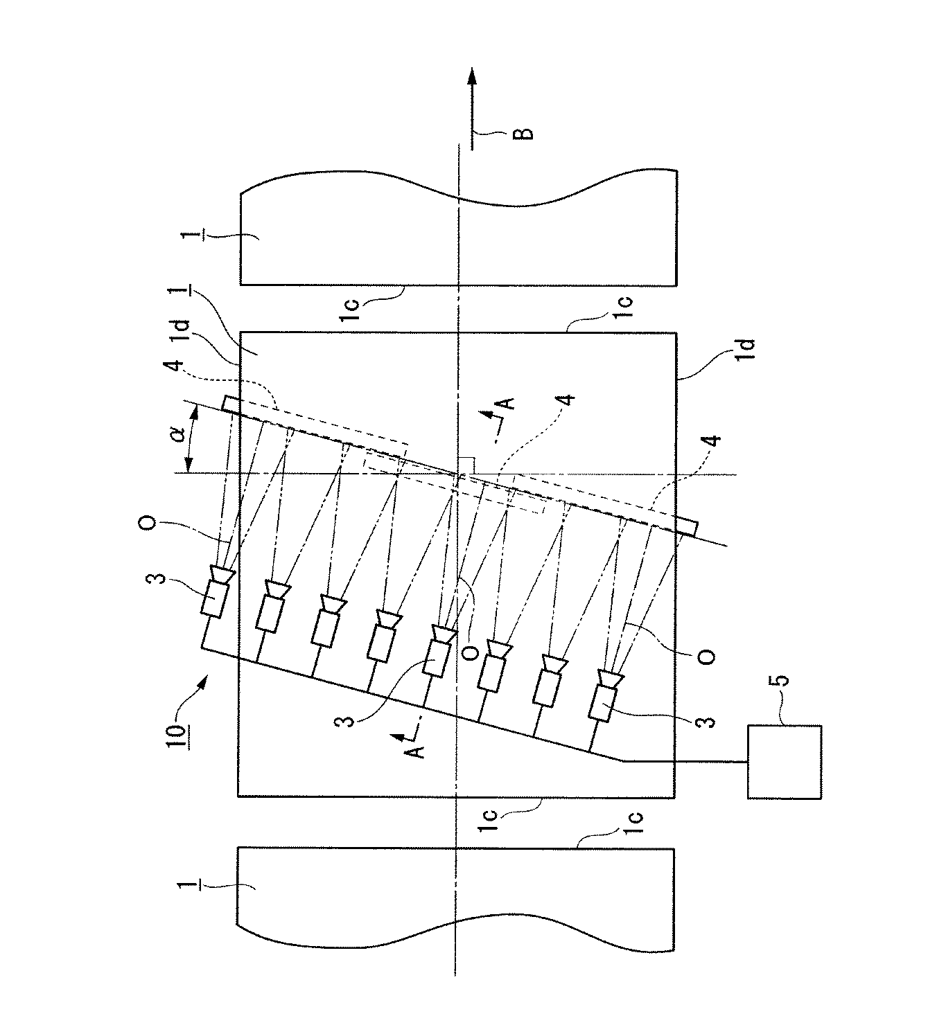
図1は、本発明の透明板の欠陥検査方法に用いることができる欠陥検査装置の概略構成を示す模式的な平面図である。図2は、図1のA−A断面図である。
Embodiments of the present invention will be described below with reference to the accompanying drawings.
FIG. 1 is a schematic plan view showing a schematic configuration of a defect inspection apparatus that can be used in the defect inspection method for a transparent plate of the present invention. 2 is a cross-sectional view taken along the line AA in FIG.
(透明板)
まず、本実施形態の欠陥検査方法の被検体である透明板1の一例について説明する。
透明板1は、図1、2に示すように、平面視矩形状の透明板本体1aの端面以外の少なくとも片方の表面に、該表面を保護するため、透明板本体1aと同じ大きさのマスキングフィルム1bを貼り付けたものである。透明板1は、後述する光照射領域に交差する一定の移動方向に移動可能に支持されている。そして、本実施形態では、このような透明板1を不図示の移動機構によって、一定の移動方向(図示矢印B方向)に水平に移動させながら、欠陥検査を行っていく。移動方向に沿って透明板1が複数存在する場合、各透明板1は、端面1c、1cが移動方向に直交するように配置され、他の端面1d、1dは移動方向に平行に配置され、各透明板1間の端面1c同士を移動方向に対向させた状態で、一定間隔を空けて移動させることが好ましい。以下では、端面1d、1dが対向する方向を、透明板1の幅方向と称する。なお、透明板1の移動速度は、欠陥検査の効率化の観点から0.01m/分以上が好ましく、欠陥の検出精度の観点から20m/分以下が好ましい。
(Transparent plate)
First, an example of the
As shown in FIGS. 1 and 2, the
透明板本体1aは、例えば、液晶表示装置を備えた携帯電話、パソコン用ディスプレイ、液晶TV,ビデオ一体型液晶TV、カーナビゲーションシステム等においては、エッジライト方式のバックライトユニットに用いる導光板などに用いることができるものである。
透明板本体1aの材質としては、ガラスや透明樹脂などが挙げられるが、軽量化が要求される分野で使用する場合には、透明樹脂を用いた透明樹脂板が好ましく、さらに好ましくは透明樹脂の中でも全光線透過率の高いメタクリル樹脂を使用する事が望ましい。
本実施形態では、メタクリル樹脂を用いた場合で説明する。
The
Examples of the material of the transparent plate
In the present embodiment, a case where a methacrylic resin is used will be described.
透明板本体1aに用いるメタクリル樹脂としては、メタクリル酸メチル単位70質量%以上100質量%以下と、メタクリル酸メチルと共重合可能なモノマー単位0質量%以上30質量%以下とからなる樹脂が好ましい。
メタクリル酸メチルと共重合可能なモノマーとしては、アクリル酸メチル、(メタ)アクリル酸エチル、(メタ)アクリル酸ブチル、(メタ)アクリル酸シクロヘキシル、(メタ)アクリル酸2−エチルヘキシル、(メタ)アクリル酸フェニル、(メタ)アクリル酸ベンジル、(メタ)アクリル酸2−ヒドロキシエチル、(メタ)アクリル酸グリシジル、(メタ)アクリル酸ジエチルアミノエチル等のメチルメタクリレート以外の(メタ)アクリル酸エステル類;エチレングリコールジ(メタ)アクリレート、トリメチロールプロパントリ(メタ)アクリレート、アリル(メタ)アクリレート、ネオペンチルグリコールジ(メタ)アクリレート等の多官能(メタ)アクリレート類;スチレン、α−メチルスチレン等の芳香族ビニル単量体類;フェニルマレイミド、シクロヘキシルマレイミド等のマレイミド類;無水マレイン酸等を例示することができる。ここで、「(メタ)アクリ」とは「メタクリ」あるいは「アクリ」を表す。
さらに、メタクリル酸メチル共重合体の耐衝撃性の向上を目的として、アクリル酸エステルを主成分とするゴム状共重合体存在下にメタクリル酸エステルを主成分とするモノマーをグラフト重合した共重合体を含む樹脂を前記メタクリル樹脂と併用することもできる。
The methacrylic resin used for the
Monomers that can be copolymerized with methyl methacrylate include methyl acrylate, ethyl (meth) acrylate, butyl (meth) acrylate, cyclohexyl (meth) acrylate, 2-ethylhexyl (meth) acrylate, and (meth) acrylic. (Meth) acrylic acid esters other than methyl methacrylate such as phenyl acid, benzyl (meth) acrylate, 2-hydroxyethyl (meth) acrylate, glycidyl (meth) acrylate, diethylaminoethyl (meth) acrylate; ethylene glycol Multifunctional (meth) acrylates such as di (meth) acrylate, trimethylolpropane tri (meth) acrylate, allyl (meth) acrylate, neopentyl glycol di (meth) acrylate; aromatic vinyl such as styrene and α-methylstyrene Monomers; It can be exemplified maleic anhydride; E sulfonyl maleimides, maleimides such as cyclohexyl maleimide. Here, “(meth) acryl” represents “methacryl” or “acryl”.
Furthermore, for the purpose of improving the impact resistance of methyl methacrylate copolymer, a copolymer obtained by graft polymerization of a monomer mainly composed of methacrylate in the presence of a rubbery copolymer mainly composed of acrylic ester. A resin containing can also be used in combination with the methacrylic resin.
マスキングフィルム1bとしては、ポリオレフィンやポロエステル等の可視光透過性を有する合成樹脂フィルムを採用することができる。光透過率は高い方が好ましいが、無色の透明フィルムには限定されず、着色された光透過性のフィルムを用いてもよい。
As the
透明板本体1aは、例えば、エッジライト方式のバックライトの導光板に用いる場合、表面を内部反射面として用いるため、表面の微小な打痕や異物付着が、不良の原因となる主な欠陥である。これらの欠陥は、一般に大きいほど、画質などに及ぼす影響が大きくなり、一定の大きさ以下であれば、許容することができる。
このような欠陥は、製造工程や移動中に、突起部または角部を有する何らかの固体により直接的な打撃を受けることで発生する場合や、マスキングフィルム1b上、あるいは透明板本体1aとマスキングフィルム1bとの間に、例えば切粉などの微小な固形物が付着し、この固形物が、例えば透明板1を載置する載置面や搬送ローラなどによって、押圧されて打痕が生じたり、切粉が表面に固着したりして発生する場合がある。
このため、透明板1の検査では、透明板本体1aの表面にすでに形成された一定の大きさ以上の打痕を検出するとともに、下流工程で打痕などの欠陥を発生させる可能性がある一定の大きさ以上の付着物、すなわちマスキングフィルム1b上あるいは透明板本体1aとマスキングフィルム1bとの間に付着した一定の大きさ以上の切粉などの固形物も検出する必要がある。
これに対して、マスキングフィルム1bは、使用時や組立時には必要に応じて剥がすものなので、マスキングフィルム1bの貼りムラや、透明板本体1aとマスキングフィルム1bとの間に気泡が挟み込まれて発生するエア噛みなどは欠陥とならない。そのため、このような貼りムラやエア噛みは検出しないようにする必要がある。
For example, when the transparent plate
Such a defect may be caused by being directly hit by some solid having protrusions or corners during the manufacturing process or movement, or on the
For this reason, in the inspection of the
On the other hand, since the
(欠陥検査装置)
次に、本実施形態の透明板の欠陥検査方法に用いる欠陥検査装置(測定系)の構成の一例について説明する。
本実施形態に係る欠陥検査装置10の概略構成は、図1、2に示すように、線状光源4、ラインCCDカメラ3(撮像手段)、および測定処理部5からなる。なお、特に図示しないが、透明板1を、水平面内で幅方向に直交する移動方向に移動するために適宜の移動機構が、移動方向に沿って設けられている。このような移動機構としては、例えば、複数の搬送ローラを回転駆動する移動機構を挙げることができる。
(Defect inspection equipment)
Next, an example of a configuration of a defect inspection apparatus (measurement system) used in the transparent plate defect inspection method of the present embodiment will be described.
As shown in FIGS. 1 and 2, the schematic configuration of the
線状光源4は、透明板1に検査光を発生して、透明板1の表面で直線状の光照射領域に検査光を投射するもので、光照射領域の大きさに応じて線状光源4を配置すればよい。本実施形態では透明板1の下方に透明板1の幅方向に沿って、3本が配置されている。これらの線状光源4は、透明板1の下面で、幅方向に連続する略線状の領域を照射できるように、平面視で端部が重なり合うような千鳥状に配置されている。
なお、本明細書で、直線状の光照射領域とは、短手幅が一定で長手方向が直線に沿って延びる帯状の光照射領域を意味する。また、略直線状の光照射領域とは、短手幅が変動する場合に該短手幅が一定範囲にあり長手方向が直線に沿って延びる領域がこの長手方向に沿って連続的に存在する帯状の光照射領域を意味する。
The linear
In addition, in this specification, a linear light irradiation area | region means the strip | belt-shaped light irradiation area | region where a short width is constant and a longitudinal direction extends along a straight line. Further, the substantially linear light irradiation region is a region where the short width is in a certain range and the longitudinal direction extends along the straight line continuously when the short width varies. It means a band-shaped light irradiation region.
各線状光源4は、本実施形態では、蛍光灯4aと反射板4bとからなる構成とされ、線状光源4の光軸Oは、透明板1表面の法線Nに対して、透明板1の移動方向下流側に角度θ(ただし、θ>0°)だけ傾斜されている。
角度θの大きさは、マスキングフィルム1bの透過率特性にもよるが、良好な透過光を得るためには、5°〜30°の範囲とすることが好ましい。
In this embodiment, each linear
Although the magnitude | size of angle (theta) is based also on the transmittance | permeability characteristic of the
なお、線状光源4に用いることができる光源は、直線状の光照射領域に検査光を投射できれば、蛍光灯4aには限定されない。例えば、ハロゲンランプなどの他の線状光源でもよい。
また、発光ダイオード、レーザーなど、発光部が線状でない光源であっても、例えば、複数個のものを直線上に配列したり、光ファイバ束などの導光手段やレンズなどの集光手段を用いて、直線状の領域に光を投射させることで、線状光源4として用いることができる。
The light source that can be used for the linear
Even if the light source is not a linear light source such as a light emitting diode or a laser, for example, a plurality of light sources are arranged in a straight line, or a light guide means such as an optical fiber bundle or a light collecting means such as a lens is provided. It can be used as the linear
ラインCCDカメラ3は、撮像光学系とラインCCDとを備え、線状光源4によって、透明板1の下面側から照射された検査光のうち、上面側に透過された透過光を撮像光学系によってラインCCDに撮像面上に結像し、光電変換して、輝度信号を測定処理部5に送出するものである。
ラインCCDカメラ3の撮像光軸は、線状光源4の光軸Oに沿うように設けられている。このため、ラインCCDカメラ3の撮像光軸は、法線Nに対して、透明板1の移動方向上流側に角度θだけ傾斜されている。
なお、ラインCCDカメラ3の撮像光学系の焦点位置は、透明板1の端面以外の両方の表面(上面および下面)が被写界深度内に入るように設定する。
The
The imaging optical axis of the
The focal position of the imaging optical system of the
ラインCCDカメラ3は、透明板1の幅方向にわたる光照射領域内のライン画像を撮像できれば1台からなる構成、または複数からなる構成としてもよいが、本実施形態では、幅方向にわたって8台を配置している。各ラインCCDカメラ3の撮像範囲は、隣り合うラインCCDカメラ3の撮像範囲と一部重複させることで、各線状光源4が形成する各光照射領域もれなく撮像できるようにしている。このため、透明板1の全幅における透過光の光量分布を測定することが可能となっている。
The
測定処理部5は、各ラインCCDカメラ3から送出された輝度信号に演算処理を施して、検査光の透過光の幅方向における光量分布を測定するものである。本実施形態では、8台のラインCCDカメラ3から得られる8組の輝度信号データから、透明板1の幅方向に沿う光量分布を表す輝度信号データを生成することができるようになっている。
また、輝度信号データに演算処理を施して、取得された光量分布の光量ムラを補正する補正係数を算出し、この補正係数を用いて、他に取得された光量分布を光量補正することができるようになっている。
また、光量補正された光量分布を予め記憶された閾値に基づいて二値化処理を行い、閾値より低輝度と判定された部分を欠陥と判定できるようになっている。
The
In addition, the luminance signal data is subjected to arithmetic processing to calculate a correction coefficient for correcting unevenness in the obtained light quantity distribution, and the other obtained light quantity distribution can be corrected for light quantity using this correction coefficient. It is like that.
Further, binarization processing is performed on the light amount distribution corrected for light amount based on a threshold value stored in advance, and a portion determined to have a luminance lower than the threshold value can be determined as a defect.
測定処理部5の装置構成は、これらの演算処理等を行う適宜のハードウェアを採用することができるが、本実施形態では、CPU、メモリ、入出力インタフェース、外部記憶装置などを備えるコンピュータによって構成し、上記各処理を、それぞれに対応するプログラムを実行することで実現している。
The apparatus configuration of the
(欠陥検査方法)
次に、本実施形態に係る透明板の欠陥検査方法について説明する。
図3は、本発明の実施形態に係る透明板の欠陥検査方法によって取得された光量補正後の光量分布の一例を示すグラフである。横軸は撮像手段の画素に対応する位置を表し、縦軸は輝度値を示す。
本方法は、(1)初期分布測定工程、(2)補正係数算出工程、(3)光量分布測定工程、(4)光量補正工程、および(5)欠陥判定工程を備える。以下、順を追って説明する。
(Defect inspection method)
Next, the defect inspection method for the transparent plate according to the present embodiment will be described.
FIG. 3 is a graph showing an example of a light amount distribution after light amount correction obtained by the transparent plate defect inspection method according to the embodiment of the present invention. The horizontal axis represents the position corresponding to the pixel of the imaging means, and the vertical axis represents the luminance value.
The method includes (1) an initial distribution measurement step, (2) a correction coefficient calculation step, (3) a light amount distribution measurement step, (4) a light amount correction step, and (5) a defect determination step. In the following, description will be given in order.
(1)初期分布測定工程
初期分布測定工程は、線状光源4とラインCCDカメラ3との間に透明板1を配置しない状態で、線状光源4を点灯して検査光を照射させ、ラインCCDカメラ3によってこの検査光による撮像を行い、線状光源4の光照射領域の長手方向に沿う光量分布を測定する工程である。この工程により線状光源の光照射量域の長手方向に沿う方向における光量ムラや、撮像手段の受光感度ムラなど、被検体の欠陥と関係しない測定系の光量ムラを求めることができる。
各ラインCCDカメラ3によって撮像され、光電変換された輝度信号データは、それぞれ測定処理部5に送出される。
各ラインCCDカメラ3から送出された輝度信号データは、各線状光源4の発光特性に基づく光量ムラと、各ラインCCDカメラ3の撮像光学系の光学特性や画素ごとの受光感度特性のバラツキとからなる光量ムラ(以下、測定系の光量ムラと称する)を含む光量分布となっている。
(1) Initial distribution measurement process In the initial distribution measurement process, the linear
Luminance signal data imaged and photoelectrically converted by each
The luminance signal data sent from each
(2)補正係数算出工程
次に、補正係数算出工程では、初期分布測定工程で取得された光量分布における測定系の光量ムラを補正する補正係数を算出する。例えば、ラインCCDカメラ3のi番目の画素における輝度値をPiとし、ラインCCDカメラ3の全画素の平均輝度値をPaveとするとき、補正係数kiとして、ki=Pave/Piを採用することができる。
各ラインCCDカメラ3の各画素の補正係数kiは、測定処理部5に記憶しておく。
なお、補正係数kiを求めるための輝度値Piは、一回の測定値には限定されず、必要に応じて、複数の測定値の時間平均を用いてもよい。
(2) Correction Coefficient Calculation Step Next, in the correction coefficient calculation step, a correction coefficient for correcting the light amount unevenness of the measurement system in the light amount distribution acquired in the initial distribution measurement step is calculated. For example, when the luminance value at the i-th pixel of the
The correction coefficient k i of each pixel of each
The luminance value P i for obtaining the correction coefficient k i is not limited to a single measurement value, and a time average of a plurality of measurement values may be used as necessary.
次に、点灯された線状光源4とラインCCDカメラ3との間で、透明板1を移動方向に移動させつつ、以下の各工程を行う。
(3)光量分布測定工程
まず、光量分布測定工程では、各ラインCCDカメラ3によって、線状光源4から光照射領域に投射される検査光のうち、透明板1を透過した透過光を撮像して、光照射領域の長手方向に沿う光量分布を測定する。この工程では、測定系の光量ムラと、被検体の欠陥による光量変化とが重畳された状態で、光照射領域の長手方向に沿う光量分布を測定することになる。
各ラインCCDカメラ3によって撮像され、光電変換された輝度信号データは、それぞれ測定処理部5に送出される。
各ラインCCDカメラ3から送出された輝度信号データは、測定系の光量ムラを含むとともに、透明板1に欠陥が存在する場合、その欠陥の影響による光量低下を含む光量分布となっている。
この光量分布でのラインCCDカメラ3のi番目の画素における輝度値をQiと表す。
Next, the following steps are performed while moving the
(3) Light quantity distribution measurement process First, in the light quantity distribution measurement process, transmitted light that has passed through the
Luminance signal data imaged and photoelectrically converted by each
The luminance signal data sent from each
The luminance value at the i-th pixel of the
(4)光量補正工程
次に光量補正工程では、光量分布測定工程で得られた光量分布に対して、補正係数算出工程で得られた補正係数を用いて光量補正を行い、測定系の光量ムラを補正する。具体的には、光量分布測定工程で測定された光量分布における各画素における輝度値Qiに対して、補正係数kiを乗じて、光量補正された輝度値qiを算出する。すなわち、qi=ki・Qiである。これにより、輝度値qiからは、輝度値Qiに含まれている測定系の光量ムラの影響が取り除かれる。
このようにして、測定系の光量ムラの影響が除去された透明板1の幅方向に光量分布が得られる。
なお、本実施形態では、2つのラインCCDカメラ3が重複する領域では、輝度値qiが2個ずつ存在するが、これらは、いずれか一方を選択してもよいし、それぞれの平均値を対応する画素の輝度値qiとして用いるようにしてもよい。
(4) Light amount correction step Next, in the light amount correction step, the light amount distribution obtained in the light amount distribution measurement step is subjected to light amount correction using the correction coefficient obtained in the correction coefficient calculation step, and the light amount unevenness of the measurement system Correct. Specifically, the luminance value q i corrected for the light amount is calculated by multiplying the luminance value Q i in each pixel in the light amount distribution measured in the light amount distribution measuring step by the correction coefficient k i . That is, q i = k i · Q i . As a result, the influence of the unevenness in the amount of light of the measurement system included in the luminance value Q i is removed from the luminance value q i .
In this way, a light quantity distribution is obtained in the width direction of the
In the present embodiment, in the region where the two
このような光量補正された光量分布においては、輝度値の低下した部分は、何らかの欠陥が存在する可能性がある。
例えば、透明板本体1a上に微小な打痕が生じたり、透明板本体1a上やマスキングフィルム1bの表面に微小な切粉などの固形物が付着したりすると、検査光が散乱されたり、吸収されたりするため、ラインCCDカメラ3に到達する光量が低下する。
例えば、図3に曲線50で示すような光量分布が得られる。この例では、位置jで最低のピークレベルとして、輝度値qjをとる略V字状の光量低下が現れる。
このような光量低下部分の最低のピークレベルと、欠陥の大きさとの間には相関関係があり、一定閾値qth以下の光量低下部分(位置mから位置nまで)には、不良となる打痕などの欠陥、もしくは欠陥となりうる切粉などの付着物が見られる。
In such a light amount distribution after the light amount correction, there is a possibility that some defect exists in the portion where the luminance value is lowered.
For example, if a minute dent is generated on the transparent plate
For example, a light amount distribution as shown by a
And the lowest peak levels of such light amount reduction portion, there is a correlation between the size of the defect, the constant threshold value q th following reduction in light quantity portion (from position m to position n), hitting to be defective Defects such as marks, or deposits such as chips that can become defects are observed.
(5)欠陥判定工程
そこで、欠陥判定工程では、測定系の光量分布に起因する光量ムラが補正によりキャンセルされた光量分布を、予め設定された閾値によって二値化処理して、閾値以下の光量の部分を欠陥と判定することとができる。すなわち光量補正工程による光量補正後の光量分布を、予め設定された閾値qthによって二値化処理して、閾値qth以下の光量の部分を欠陥と判定し、欠陥部分の画素位置を測定処理部5に記憶する。ここで閾値の設定は、従前の目視による判定基準に合わせることにする。
そして、光量分布測定工程および光量補正工程を、透明板1の移動に合わせて一定のタイミングで繰り返すことにより、透明板1上での2次元的な欠陥分布の情報が取得され、測定処理部5に蓄積されていく。
1枚の透明板1の検査が終了したら、測定処理部5に記憶された前記二値化処理による欠陥判定の情報に基づいて、透明板1の合否の判定を行う。そして、次の透明板1の検査を開始する。
(5) Defect determination step Therefore, in the defect determination step, the light amount distribution in which the light amount unevenness caused by the light amount distribution of the measurement system is canceled by correction is binarized by a preset threshold value, and the light amount below the threshold value This part can be determined as a defect. That is, the light amount distribution after the light amount correction in the light amount correction step is binarized by a preset threshold value q th , a portion having a light amount equal to or less than the threshold value q th is determined as a defect, and the pixel position of the defective portion is measured. Store in
Then, the information on the two-dimensional defect distribution on the
When the inspection of one
次の検査の開始時には、測定系の光量ムラが経時的に安定している場合には、上記の初期分布測定工程、および補正係数算出工程は省略することができる。
ただし、線状光源4の光量分布に経時変化があるような場合などでは、適宜、初期分布測定工程、および補正係数算出工程を行うようにすることが好ましい。例えば、複数の透明板1を間を置いて連続的に移動させる場合に、各透明板1の離間された部分が線状光源4およびラインCCDカメラ3の間を通過するタイミングで、初期分布測定工程、および補正係数算出工程行うようにすることができる。
At the start of the next inspection, if the unevenness in the amount of light in the measurement system is stable over time, the initial distribution measurement step and the correction coefficient calculation step can be omitted.
However, when there is a change with time in the light amount distribution of the linear
本実施形態の透明板の欠陥検査方法によれば、補正係数算出工程で算出された補正係数を光量分布測定工程で測定された光量分布に乗ずることで、測定系の光量ムラを補正することができるので、線状光源4に光量ムラが存在したり、ラインCCDカメラ3に受光感度バラツキが存在したりする場合にも、マスキングフィルム1bを貼り付けた透明板1における欠陥の検出精度を向上することができる。
According to the defect inspection method for a transparent plate of this embodiment, the light quantity unevenness of the measurement system can be corrected by multiplying the light quantity distribution measured in the light quantity distribution measurement process by the correction coefficient calculated in the correction coefficient calculation process. Therefore, even when there is unevenness in the amount of light in the linear
また、本実施形態では、線状光源4の光軸Oを透明板1の法線Nに対して傾斜させているため、端面1cに検査光が斜め入射して、透過光になるため、ラインCCDカメラ3上に、端面1cの画像が投影される。このため、端面1cに切欠きや打痕などの欠陥が存在する場合に、このような欠陥の検出を行うことが可能となる。
また、透明板1の移動に伴って変化する、欠陥が存在しない部分における光量分布を検知することで、端面1cの位置や形状が明瞭に検知される。
したがって、ラインCCDカメラ3が取得する画像上から、端面1cからの移動方向における欠陥の位置を正確に特定することが可能となる。
角度θが小さすぎる場合には、端面1cに入射して透過する光成分が少なすぎるため、端面1cの欠陥による光量低下量が少なくなり、欠陥の検出精度が劣ってしまう。また、端面1cの位置を判別することも難しくなるため、検出された欠陥が端面1cに存在するかどうか正確には判断できなくなる。
また、角度θが大きすぎる場合、透明板1の端面1cでの欠陥検出精度および端面1cの位置の判別精度は向上できるものの、透明板1の表面に対する入射角が大きくなりすぎ、この斜め入射によるマスキングフィルム1bでの光の吸収が大きくなりすぎる。このため、ラインCCDカメラ3に十分な光量が到達しなくなり、透明板1の表面での欠陥の検出精度が悪くなる。
In the present embodiment, since the optical axis O of the linear
Further, the position and shape of the end face 1c can be clearly detected by detecting the light amount distribution in the portion where there is no defect, which changes as the
Therefore, the position of the defect in the moving direction from the end face 1c can be accurately specified from the image acquired by the
When the angle θ is too small, the amount of light component incident on and transmitted through the end face 1c is too small, so that the amount of light reduction due to a defect on the end face 1c is reduced and the defect detection accuracy is deteriorated. Further, since it becomes difficult to determine the position of the
If the angle θ is too large, the defect detection accuracy on the
次に、本実施形態の変形例について説明する。
図4は、本発明の実施形態の変形例に係る透明板の欠陥検査方法に用いることができる欠陥検査装置の概略構成を示す模式的な平面図である。
Next, a modification of this embodiment will be described.
FIG. 4 is a schematic plan view showing a schematic configuration of a defect inspection apparatus that can be used in the defect inspection method for a transparent plate according to a modification of the embodiment of the present invention.
本変形例は、上記実施形態の透明板の欠陥検査方法において、線状光源4の光照射領域を、透明板1の幅方向に対して斜めに傾斜させた配置として、上記実施形態の各工程を同様に行うものである。
このため、図4に示すように、欠陥検査装置10において、各線状光源4、各ラインCCDカメラ3の位置を水平面内で、それぞれ角度α(ただし、αは角度)だけ回転させた配置とする。
This modification is different from the defect inspection method for a transparent plate according to the above-described embodiment in that each light irradiation region of the linear
Therefore, as shown in FIG. 4, in the
本変形例によれば、線状光源4からの検査光が、透明板1の端面1cおよび端面1dに斜め入射することになる。このため、端面1dに存在する欠陥も端面1cに存在する欠陥と同時に検査することができる。
According to this modification, the inspection light from the linear
なお、上記の説明では、被検体が矩形板状の場合の例で説明したが、被検体は、一定幅で移動方向に連続されたシート状の透明板であってもよい。 In the above description, the example in which the subject has a rectangular plate shape has been described. However, the subject may be a sheet-like transparent plate having a constant width and continuous in the moving direction.
また、上記の説明では、線状光源が被検体の幅よりも短い複数からなり、端部が重複するように千鳥状に配置された場合の例で説明したが、被検体の幅よりも長い1つの線状光源を用いてもよい。 In the above description, the linear light source is composed of a plurality of shorter than the width of the subject and arranged in a staggered manner so that the end portions overlap each other. However, the linear light source is longer than the width of the subject. One linear light source may be used.
以下では、本実施形態の透明板の欠陥検査方法の実施例について説明する。
まず、本実施例に共通する欠陥検査装置10の設定条件、および被検体の条件について説明する。
欠陥検査装置10の線状光源4としては、蛍光灯4aとして、100V、65Wのもの3本を千鳥状に配置し、蛍光灯4aの裏面に反射板4bを取り付けた構成とした。
光軸Oの透明板1の法線Nに対する角度θは、θ=10°とした。
ラインCCDカメラ3としては、撮像光学系として、焦点距離50mm、Fナンバー2.8のレンズYK5028(商品名;ペンタックス株式会社製)を装着した、デジタル出力ラインCCDカメラMKS−7450−40(商品名;三菱レイヨン株式会社製)を8組、線状光源4の光軸Oに合わせて、図1に示すように、対向して配置した。
Below, the Example of the defect inspection method of the transparent plate of this embodiment is described.
First, the setting conditions of the
As the linear
The angle θ of the optical axis O with respect to the normal N of the
As the
透明板本体1aとしては、メタクリル樹脂であるアクリライト(登録商標)LX N865(商品名;三菱レイヨン株式会社製)を用い、幅×長さ×厚さが、1380mm×11220mm×8mmの矩形板に加工したものを採用した。
透明板1は、この透明板本体1aの板厚方向の表面にマスキングフィルム1bとして、無色透明およびオレンジ透明である厚さ90μmのポリエチレン保護フィルムを、エチレン−酢酸ビニル共重合体層を介して積層させた。
そして、上記実施形態に説明した初期分布測定工程、補正係数算出工程、光量分布測定工程、光量補正工程、および欠陥判定工程を実施した。
光量補正工程後における欠陥のない位置における輝度値qiは、図3に示すように100であった。また、欠陥判定工程における閾値qthは、不良とすべき欠陥の大きさと輝度値との相関関係を事前の測定と目視判定との結果から、qth=55に設定した。
なお、前記透明板1を3m/分で移動させながら、0.02ms毎に幅方向の光量分布の測定を行った。
Acrylic (registered trademark) LX N865 (trade name; manufactured by Mitsubishi Rayon Co., Ltd.), which is a methacrylic resin, is used as the transparent plate
The
Then, the initial distribution measurement process, the correction coefficient calculation process, the light quantity distribution measurement process, the light quantity correction process, and the defect determination process described in the above embodiment were performed.
The luminance value q i at a position having no defect after the light amount correction step was 100 as shown in FIG. In addition, the threshold value q th in the defect determination step is set to q th = 55 based on the results of prior measurement and visual determination of the correlation between the size of the defect to be defective and the luminance value.
In addition, the light quantity distribution in the width direction was measured every 0.02 ms while moving the
以上の条件で、透明板1の欠陥検査を行い、光量低下部におけるピークレベル(図3の輝度値qj)とその位置を記録した。そして、各位置の透明板1の状態を拡大観察し、異常の種別と大きさを調べ、従来の欠陥の判定基準によって不良か合格かを判定した。
6例の測定結果について、表1に示す。
Under the above conditions, the defect inspection of the
Table 1 shows the measurement results of six cases.
測定例1〜3では、光量低下部に対応する透明板1の表面に打痕が認められ、それぞれの大きさは、φ1.0mm、φ0.6mm、φ0.4mmであった。このとき、ピークレベルは、それぞれ11、21、25であった。これらのピークレベルは、いずれも閾値55より小さいため、本方法では、不良と判定された。一方、従来の目視判定基準でも不良と判定された。
このように、透明板1に打痕が存在した場合、打痕の大きさが大きいほど、ピークレベルが減少し、ピークレベルの大きさに適切な閾値を設けることで、打痕による不良が検出できることが確認できた。
In Measurement Examples 1 to 3, dents were observed on the surface of the
In this way, when a dent is present on the
測定例4、6では、光量低下部に対応する透明板1に切粉の付着が認められ、それぞれの大きさは、φ0.7mm、φ0.2mmであった。このとき、ピークレベルは、それぞれ36、83であった。このため、測定例4、6は、本方法では、それぞれ不良、合格と判定された。一方、従来の目視判定基準でもそれぞれ不良、合格と判定された。
このように、透明板1に切粉が付着した場合、切粉の大きさが大きいほど、ピークレベルが減少し、ピークレベルの大きさに適切な閾値を設けることで、切粉による不良が検出できることが確認できた。
In Measurement Examples 4 and 6, adhesion of chips was observed on the
Thus, when chips adhere to the
測定例5では、光量低下部に対応する透明板1におけるマスキングフィルム1bが、エア噛みよってφ1.0の浮きが認められた。マスキングフィルム1bを剥がせば消失するものなので、合格と判定されるべきものである。このとき、ピークレベルは、76であった。このため、本方法では、合格と判定された。
このように、透明板1のマスキングフィルム1bが、エア噛みによって浮いた状態では、透過光の吸収や散乱が余り起こらないため、ピークレベルの低下は少なく、例えば、測定例1のように同じ大きさの打痕とは、明確に区別することができる。
したがって、本方法では、ピークレベルの大きさに適切な閾値を設けることで、不良とならないエア噛みによって、誤判定を起こさないようにすることができることが確認できた。
In the measurement example 5, the masking
Thus, in the state where the
Therefore, in this method, it has been confirmed that by providing an appropriate threshold for the magnitude of the peak level, it is possible to prevent erroneous determination due to air biting that does not become defective.
1 透明板(被検体)
1a 透明板本体
1b マスキングフィルム
3 ラインCCDカメラ(撮像手段)
4 線状光源
5 測定処理部
10 欠陥検査装置
N 法線
O 光軸
1 Transparent plate (subject)
1a
4 Linear
Claims (4)
前記線状光源を、前記検査光の光軸が前記被検体の表面の法線に対して角度θ(ただし、θ>0°)だけ傾斜し、かつ前記光照射領域が前記被検体を幅方向に横断するように配置するとともに、前記撮像手段を、前記検査光の光軸に沿う方向から、前記光照射領域を長手方向に沿って撮像できるように配置し、以下の工程を行うことにより、前記被検体の欠陥検査を行う透明板の欠陥検査方法。
(1)線状光源と撮像手段の間に被検体を配置しない状態で、前記線状光源によって検査光を投射し、前記撮像手段によって前記検査光を撮像して光照射領域の長手方向に沿う光量分布を測定する初期分布測定工程
(2)初期分布測定工程で測定された光量分布における光量ムラを補正する補正係数を算出する補正係数算出工程
(3)線状光源と撮像手段との間に被検体を配置した状態で、
前記撮像手段によって、検査光の前記被検体からの透過光を撮像して光照射領域の長手方向に沿う光量分布を測定する光量分布測定工程
(4)光量分布測定工程で測定された光量分布を、補正係数算出工程で算出された補正係数を用いて光量補正する光量補正工程
(5)光量補正工程による光量補正後の光量分布を、予め設定された閾値によって二値化処理して、前記閾値以下の光量の部分を欠陥と判定する欠陥判定工程 Using a transparent plate with a light-transmitting masking film affixed to the surface as a subject, using a linear light source that projects inspection light onto a substantially linear light irradiation region, from one surface side of the subject Defect inspection of a transparent plate that projects the inspection light onto the subject and images the transmitted light of the inspection light by an imaging means disposed on the other surface side of the subject to inspect the subject for defects A method,
The linear light source is tilted by an angle θ (where θ> 0 °) with respect to the normal of the surface of the subject with the optical axis of the inspection light, and the light irradiation region crosses the subject in the width direction. By arranging the imaging means so as to image the light irradiation region along the longitudinal direction from the direction along the optical axis of the inspection light, and performing the following steps: A transparent plate defect inspection method for inspecting a defect of the object.
(1) In a state where no subject is arranged between the linear light source and the imaging means, the inspection light is projected by the linear light source, the inspection light is imaged by the imaging means, and the longitudinal direction of the light irradiation region is along Initial distribution measuring step for measuring the light amount distribution (2) Correction coefficient calculating step for calculating a correction factor for correcting the light amount unevenness in the light amount distribution measured in the initial distribution measuring step (3) Between the linear light source and the imaging means With the subject placed,
The light quantity distribution measurement step (4) of measuring the light amount distribution along the longitudinal direction of the light irradiation region by imaging the transmitted light of the inspection light from the subject by the imaging means (4) The light amount distribution measured in the light amount distribution measurement step A light amount correction step for correcting the light amount by using the correction coefficient calculated in the correction coefficient calculation step. (5) The light amount distribution after the light amount correction by the light amount correction step is binarized by a preset threshold value, and the threshold value Defect determination process for determining the following light quantity as a defect
前記線状光源は、前記検査光の光軸が前記被検体の表面の法線に対して前記移動方向下流側に傾斜した配置とされ、
前記被検体を前記移動方向に移動させつつ、少なくとも前記光量分布測定工程および前記光量補正工程を繰り返して行う請求項1または2に記載の透明板の欠陥検査方法。 The subject is held so as to be movable in a certain movement direction intersecting the light irradiation region,
The linear light source is arranged such that the optical axis of the inspection light is inclined to the downstream side in the movement direction with respect to the normal of the surface of the subject.
3. The defect inspection method for a transparent plate according to claim 1, wherein at least the light amount distribution measurement step and the light amount correction step are repeated while moving the subject in the moving direction.
前記線状光源は、前記検査光の光軸が前記被検体の表面の法線に対して角度θ(ただし、θ>0°)だけ傾斜され、かつ前記光照射領域が前記被検体を幅方向に横断するように配置され、
前記撮像手段は、前記検査光の光軸に沿う方向から、前記光照射領域を長手方向に沿って撮像できるように配置され、
前記線状光源と前記撮像手段の間に前記被検体を配置しない状態で、
前記線状光源によって前記検査光を投射し、前記撮像手段によって前記検査光を撮像して前記光照射領域の長手方向に沿う光量分布を測定する初期分布測定を行い、
該初期分布測定で測定された光量分布における光量ムラを補正する補正係数を算出し、
前記線状光源と前記撮像手段との間に前記被検体を配置した状態で、
前記撮像手段によって、前記検査光の前記被検体からの透過光を撮像して前記光照射領域の長手方向に沿う光量分布を測定する光量分布測定を行い、
該光量分布測定で測定された光量分布を、前記補正係数を用いて光量補正を行い、
該光量補正後の光量分布を、予め設定された閾値によって二値化処理して、前記閾値以下の光量の部分を欠陥と判定する測定処理部を備える透明板の欠陥検査装置。 Using a transparent plate with a light-transmitting masking film affixed to the surface as a subject, using a linear light source that projects inspection light onto a substantially linear light irradiation region, from one surface side of the subject Defect inspection of a transparent plate that projects the inspection light onto the subject and images the transmitted light of the inspection light by an imaging means disposed on the other surface side of the subject to inspect the subject for defects A device,
In the linear light source, the optical axis of the inspection light is inclined by an angle θ (where θ> 0 °) with respect to the normal line of the surface of the subject, and the light irradiation region extends the subject in the width direction. Arranged to cross
The imaging means is arranged so that the light irradiation area can be imaged along the longitudinal direction from the direction along the optical axis of the inspection light,
In a state where the subject is not disposed between the linear light source and the imaging means,
Projecting the inspection light by the linear light source, imaging the inspection light by the imaging means, and performing an initial distribution measurement for measuring a light amount distribution along a longitudinal direction of the light irradiation region;
Calculating a correction coefficient for correcting the light amount unevenness in the light amount distribution measured in the initial distribution measurement;
With the subject placed between the linear light source and the imaging means,
Performing a light amount distribution measurement for measuring a light amount distribution along a longitudinal direction of the light irradiation region by imaging the transmitted light from the subject of the inspection light by the imaging means,
The light amount distribution measured by the light amount distribution measurement is corrected using the correction coefficient,
A transparent plate defect inspection apparatus comprising: a measurement processing unit that binarizes the light amount distribution after the light amount correction with a preset threshold value and determines a portion of the light amount equal to or less than the threshold value as a defect.
Priority Applications (1)
| Application Number | Priority Date | Filing Date | Title |
|---|---|---|---|
| JP2008079068A JP2009236493A (en) | 2008-03-25 | 2008-03-25 | Flaw inspecting method of transparent plate and flaw inspection device |
Applications Claiming Priority (1)
| Application Number | Priority Date | Filing Date | Title |
|---|---|---|---|
| JP2008079068A JP2009236493A (en) | 2008-03-25 | 2008-03-25 | Flaw inspecting method of transparent plate and flaw inspection device |
Publications (1)
| Publication Number | Publication Date |
|---|---|
| JP2009236493A true JP2009236493A (en) | 2009-10-15 |
Family
ID=41250646
Family Applications (1)
| Application Number | Title | Priority Date | Filing Date |
|---|---|---|---|
| JP2008079068A Pending JP2009236493A (en) | 2008-03-25 | 2008-03-25 | Flaw inspecting method of transparent plate and flaw inspection device |
Country Status (1)
| Country | Link |
|---|---|
| JP (1) | JP2009236493A (en) |
Cited By (8)
| Publication number | Priority date | Publication date | Assignee | Title |
|---|---|---|---|---|
| JP2012137980A (en) * | 2010-12-27 | 2012-07-19 | Fuji Mach Mfg Co Ltd | Image generating apparatus and image generating method |
| JP2012163358A (en) * | 2011-02-03 | 2012-08-30 | Nippon Electric Glass Co Ltd | Glass plate end face imaging apparatus and imaging method therefor |
| WO2014192334A1 (en) * | 2013-05-30 | 2014-12-04 | 住友化学株式会社 | Defect inspection apparatus, and production system of optical display device |
| DE102014115318A1 (en) * | 2014-10-21 | 2016-04-21 | cibite AG | Method and device for checking the transmittance of a flat glass substrate |
| DE102014115317A1 (en) * | 2014-10-21 | 2016-04-21 | cibite AG | Method and device for determining the transmittance of a flat glass substrate |
| JP2017538117A (en) * | 2014-12-05 | 2017-12-21 | ケーエルエー−テンカー コーポレイション | Apparatus, method and computer program product for workpiece defect detection |
| CN112884698A (en) * | 2019-11-14 | 2021-06-01 | 胜丽国际股份有限公司 | Defect detection method for sensor packaging structure |
| JP2021135125A (en) * | 2020-02-26 | 2021-09-13 | トヨタ自動車株式会社 | Inspection method and inspection device of membrane electrode assembly |
-
2008
- 2008-03-25 JP JP2008079068A patent/JP2009236493A/en active Pending
Cited By (25)
| Publication number | Priority date | Publication date | Assignee | Title |
|---|---|---|---|---|
| US9474195B2 (en) | 2010-12-27 | 2016-10-18 | Fuji Machine Mfg. Co., Ltd. | Image generating apparatus and image generating method |
| JP2012137980A (en) * | 2010-12-27 | 2012-07-19 | Fuji Mach Mfg Co Ltd | Image generating apparatus and image generating method |
| JP2012163358A (en) * | 2011-02-03 | 2012-08-30 | Nippon Electric Glass Co Ltd | Glass plate end face imaging apparatus and imaging method therefor |
| WO2014192334A1 (en) * | 2013-05-30 | 2014-12-04 | 住友化学株式会社 | Defect inspection apparatus, and production system of optical display device |
| JP2014234999A (en) * | 2013-05-30 | 2014-12-15 | 住友化学株式会社 | Defect inspection device and production system of optical display device |
| US10557796B2 (en) | 2014-10-21 | 2020-02-11 | cibite AG | Method and device for determining the transmittance of a flat glass substrate |
| DE102014115318A1 (en) * | 2014-10-21 | 2016-04-21 | cibite AG | Method and device for checking the transmittance of a flat glass substrate |
| DE102014115317A1 (en) * | 2014-10-21 | 2016-04-21 | cibite AG | Method and device for determining the transmittance of a flat glass substrate |
| US20180128740A1 (en) * | 2014-10-21 | 2018-05-10 | cibite AG | Method and device for determining the transmittance of a flat glass substrate |
| US20180266966A1 (en) * | 2014-10-21 | 2018-09-20 | cibite AG | Method and device for verifying the transmittance of a flat glass substrate |
| US10352874B2 (en) * | 2014-10-21 | 2019-07-16 | Gibite AG | Method and device for verifying the transmittance of a flat glass substrate |
| US10935503B2 (en) | 2014-12-05 | 2021-03-02 | Kla Corporation | Apparatus, method and computer program product for defect detection in work pieces |
| JP2023174984A (en) * | 2014-12-05 | 2023-12-08 | ケーエルエー コーポレイション | Semiconductor device defect detection apparatus and method |
| JP7755668B2 (en) | 2014-12-05 | 2025-10-16 | ケーエルエー コーポレイション | Defect detection device for individual semiconductor devices |
| US11105839B2 (en) | 2014-12-05 | 2021-08-31 | Kla Corporation | Apparatus, method and computer program product for defect detection in work pieces |
| JP2024026780A (en) * | 2014-12-05 | 2024-02-28 | ケーエルエー コーポレイション | Defect detection equipment for singulated semiconductor devices |
| JP2021175987A (en) * | 2014-12-05 | 2021-11-04 | ケーエルエー コーポレイション | Device for detecting defects of individualized semiconductor device |
| JP2021182005A (en) * | 2014-12-05 | 2021-11-25 | ケーエルエー コーポレイション | Apparatus and method for defect detection in work pieces |
| US11726126B2 (en) | 2014-12-05 | 2023-08-15 | Kla Corporation | Apparatus, method and computer program product for defect detection in work pieces |
| JP7373527B2 (en) | 2014-12-05 | 2023-11-02 | ケーエルエー コーポレイション | Workpiece defect detection device and method |
| US11892493B2 (en) | 2014-12-05 | 2024-02-06 | Kla Corporation | Apparatus, method and computer program product for defect detection in work pieces |
| JP2017538117A (en) * | 2014-12-05 | 2017-12-21 | ケーエルエー−テンカー コーポレイション | Apparatus, method and computer program product for workpiece defect detection |
| CN112884698B (en) * | 2019-11-14 | 2023-11-28 | 同欣电子工业股份有限公司 | Defect detection method of sensor packaging structure |
| CN112884698A (en) * | 2019-11-14 | 2021-06-01 | 胜丽国际股份有限公司 | Defect detection method for sensor packaging structure |
| JP2021135125A (en) * | 2020-02-26 | 2021-09-13 | トヨタ自動車株式会社 | Inspection method and inspection device of membrane electrode assembly |
Similar Documents
| Publication | Publication Date | Title |
|---|---|---|
| JP2009236493A (en) | Flaw inspecting method of transparent plate and flaw inspection device | |
| JP5909751B2 (en) | Flat glass foreign matter inspection apparatus and inspection method | |
| WO2010024082A1 (en) | Defect inspecting system, and defect inspecting method | |
| JP5274622B2 (en) | Defect inspection apparatus and method | |
| JP2001519890A (en) | Techniques for detecting three-dimensional defect locations in transparent structures | |
| JP2003344301A (en) | Inspection method and inspection device for polarizing film | |
| US20120044346A1 (en) | Apparatus and method for inspecting internal defect of substrate | |
| KR20230144770A (en) | Method for inspecting defects of optical film | |
| JP2006071284A (en) | Inside and outside discrimination method of flaw of glass substrate | |
| CN1666100A (en) | Optical measuring method and device therefor | |
| KR20090032994A (en) | Inspection device | |
| WO2012153718A1 (en) | Method for testing end face of glass sheet and device for testing end face of glass sheet | |
| KR101409217B1 (en) | Inspection apparatus and inspection method of attached substrate | |
| CN101065657A (en) | System and method for inspecting a light-management film and the method of making the light-management film | |
| WO2022123859A1 (en) | Optical film edge detection method | |
| JP2009053146A (en) | Inspection method for foreign matter in transparent plate | |
| CN116678895B (en) | Screen scratch detection method, system and storage medium | |
| KR100749954B1 (en) | Inspection method of polarizing film and inspection device of polarizing film applied thereto | |
| CN111751386B (en) | Machine vision optical detection system and method | |
| KR100971081B1 (en) | Polarizing Film Inspection Method | |
| JP3149336B2 (en) | Optical member inspection device | |
| JP4855193B2 (en) | Thin plate inspection equipment | |
| JP2016125817A (en) | Inspection system, and inspection method | |
| KR20130098113A (en) | Inspection apparatus and inspection method of attached substrate | |
| JP2005156416A (en) | Glass substrate inspection method and glass substrate inspection apparatus |