JP2008206143A - Imaging device having image processing function - Google Patents
Imaging device having image processing function Download PDFInfo
- Publication number
- JP2008206143A JP2008206143A JP2008013121A JP2008013121A JP2008206143A JP 2008206143 A JP2008206143 A JP 2008206143A JP 2008013121 A JP2008013121 A JP 2008013121A JP 2008013121 A JP2008013121 A JP 2008013121A JP 2008206143 A JP2008206143 A JP 2008206143A
- Authority
- JP
- Japan
- Prior art keywords
- pixel
- memory
- column
- image processing
- value
- Prior art date
- Legal status (The legal status is an assumption and is not a legal conclusion. Google has not performed a legal analysis and makes no representation as to the accuracy of the status listed.)
- Pending
Links
- 238000012545 processing Methods 0.000 title claims abstract description 136
- 238000003384 imaging method Methods 0.000 title claims abstract description 43
- 230000015654 memory Effects 0.000 claims abstract description 170
- 239000011159 matrix material Substances 0.000 claims abstract description 14
- 230000006870 function Effects 0.000 claims abstract description 12
- 230000003936 working memory Effects 0.000 claims description 59
- 238000000034 method Methods 0.000 claims description 40
- 230000003287 optical effect Effects 0.000 claims description 18
- 210000001747 pupil Anatomy 0.000 claims description 18
- 230000008602 contraction Effects 0.000 claims description 17
- 230000007704 transition Effects 0.000 claims description 14
- 238000003860 storage Methods 0.000 claims description 4
- 230000005611 electricity Effects 0.000 claims 3
- 238000011946 reduction process Methods 0.000 claims 1
- 238000001514 detection method Methods 0.000 description 29
- 238000010586 diagram Methods 0.000 description 27
- 230000008569 process Effects 0.000 description 24
- 238000007792 addition Methods 0.000 description 22
- 238000004364 calculation method Methods 0.000 description 18
- 230000004434 saccadic eye movement Effects 0.000 description 10
- 239000013598 vector Substances 0.000 description 6
- 238000004088 simulation Methods 0.000 description 5
- 210000005252 bulbus oculi Anatomy 0.000 description 4
- 230000004461 rapid eye movement Effects 0.000 description 4
- 239000003990 capacitor Substances 0.000 description 3
- 230000012447 hatching Effects 0.000 description 3
- 238000003708 edge detection Methods 0.000 description 2
- 230000000694 effects Effects 0.000 description 2
- 238000011156 evaluation Methods 0.000 description 2
- 238000009499 grossing Methods 0.000 description 2
- 238000004519 manufacturing process Methods 0.000 description 2
- 230000000007 visual effect Effects 0.000 description 2
- 230000003321 amplification Effects 0.000 description 1
- 230000008901 benefit Effects 0.000 description 1
- 230000015556 catabolic process Effects 0.000 description 1
- 230000008859 change Effects 0.000 description 1
- 238000007796 conventional method Methods 0.000 description 1
- 238000009826 distribution Methods 0.000 description 1
- 239000000284 extract Substances 0.000 description 1
- 238000000605 extraction Methods 0.000 description 1
- 210000001508 eye Anatomy 0.000 description 1
- 230000004424 eye movement Effects 0.000 description 1
- 238000003706 image smoothing Methods 0.000 description 1
- 230000001678 irradiating effect Effects 0.000 description 1
- 230000009191 jumping Effects 0.000 description 1
- 238000003199 nucleic acid amplification method Methods 0.000 description 1
- 230000002093 peripheral effect Effects 0.000 description 1
- 230000009467 reduction Effects 0.000 description 1
- 238000011160 research Methods 0.000 description 1
- 230000003068 static effect Effects 0.000 description 1
Images


Landscapes
- Position Input By Displaying (AREA)
- Transforming Light Signals Into Electric Signals (AREA)
- Studio Devices (AREA)
Abstract
【課題】高速な画像処理機能を備えた解像度の高い撮像装置を提供する。
【解決手段】撮像装置100は、マトリクス状に配置され、それぞれが受光した光の量を電気量に変換する画素である複数の受光回路101と、各受光回路101で得られた電気量の値を、各受光回路101に対応付けて保持するメモリ302と、マトリクスの列ごとに備えられる処理部103とを備え、処理部103は、メモリ302に保持されているうち少なくとも一部の列方向に連続する複数個の値を、保持するための作業用メモリ203と、作業用メモリ203に保持されている値を用いて、所定の画像処理を行う画像処理回路204とを備える。
【選択図】図3A high-resolution imaging device having a high-speed image processing function is provided.
An imaging apparatus includes a plurality of light receiving circuits that are pixels arranged in a matrix and that convert the amount of received light into an electric quantity, and values of electric quantities obtained by the respective light receiving circuits. Are stored in association with each light receiving circuit 101 and a processing unit 103 provided for each column of the matrix, and the processing unit 103 is arranged in at least a part of the column directions. A work memory 203 for holding a plurality of continuous values, and an image processing circuit 204 for performing predetermined image processing using the values held in the work memory 203 are provided.
[Selection] Figure 3
Description
本発明は、画像処理機能を備えた撮像装置、特に、視線検出機能をもつ画素並列構成のVision Chipに好適な撮像装置に関する。 The present invention relates to an imaging apparatus having an image processing function, and more particularly to an imaging apparatus suitable for a Vision Chip having a pixel parallel configuration having a line-of-sight detection function.
視線情報は、計算機への情報入力方法などとして有用なユーザインタフェースであることが知られているが、現在の一般的な視線検出装置はビデオカメラと画像処理用の計算機からなる高価で大掛かりなシステムである。そのため、その応用は学術研究などの特殊な分野に限られているのが現状である。また眼球運動には、サッケード(急速眼球運動)と呼ばれる、角速度が600[deg/s]にも達する非常に高速なものがあることが知られている。このサッケードは、無意識に起こる視線の跳躍であり、ユーザインタフェースへの応用が有用であることが提案されているが(非特許文献1、2参照)、その速度のために、60Hz程度のビデオレートでの視線検出では追尾が不可能である。高速度カメラを用いてサッケードの検出・追尾に対応したシステムも存在するが、システムが物理的に大規模・高価であり、また視線情報生成までの遅延(レイテンシ)が大きく、リアルタイムでの検出は非現実的である。発明者らは、画素ごとに受光素子と処理回路を置く、いわゆるVision Chipの構成により、サッケードに対応した視線検出・追尾のための高機能イメージセンサのアーキテクチャを検討・実装し、基礎的な評価を行ってきた(非特許文献3、4参照)。
しかしながら、画素ごとに受光素子と処理回路を置く構成では、画素並列構成をとるため画素の面積が大きく、画素数が16×16と極めて少ないという問題があり、解像度が低いため、高精度な視線の検出が困難であるという課題がある。 However, in the configuration in which the light receiving element and the processing circuit are arranged for each pixel, there is a problem in that the pixel area is large and the number of pixels is as small as 16 × 16 because of the pixel parallel configuration. There is a problem that it is difficult to detect.
上記課題に鑑み、本発明は、VGA程度の解像度を実現し急速眼球運動に対応する視線検出機能を持つVision Chip、すなわち、高速な画像処理機能を備えた解像度の高い撮像装置を提供することを目的とする。 In view of the above problems, the present invention provides a vision chip that realizes a resolution of about VGA and has a line-of-sight detection function corresponding to rapid eye movement, that is, a high-resolution imaging device having a high-speed image processing function. Objective.
上記課題を解決するために、本発明の撮像装置は、画像処理機能を備える撮像装置であって、マトリクス状に配置され、それぞれが受光した光の量を電気量に変換する画素である複数の受光回路と、各前記受光回路で得られた電気量の値を、各前記受光回路に対応付けて保持するメモリと、前記マトリクスの列ごとに備えられる処理部とを備え、前記処理部は、前記メモリに保持されているうち少なくとも一部の列方向に連続する複数個の値を保持するための作業用メモリと、前記作業用メモリに保持されている値を用いて、所定の画像処理を行う画像処理回路とを備えることを特徴とする。 In order to solve the above problems, an imaging apparatus according to the present invention is an imaging apparatus having an image processing function, and is arranged in a matrix, each of which is a plurality of pixels that convert the amount of received light into an electrical quantity. A light receiving circuit, a memory that holds the value of the electric quantity obtained in each light receiving circuit in association with each light receiving circuit, and a processing unit provided for each column of the matrix, the processing unit, Predetermined image processing is performed using a working memory for holding a plurality of values that are continuous in at least a part of column directions held in the memory, and a value held in the working memory. And an image processing circuit for performing the processing.
また、本発明において、前記作業用メモリは、前記マトリクスの各列において処理対象となる画素を中心として列方向に連続する3個の値を保持するメモリ領域を有し、前記撮像装置は、さらに、前記各列において同一行の画素が並行処理されるよう、クロックごとに各列で処理対象となる画素を行方向にシフトし、処理対象となる画素を中心として列方向に連続する3画素に対応する各前記メモリに保持されている値を読み出して、各前記メモリに対応する前記作業用メモリに書き込むメモリコントローラを備え、各列の前記画像処理回路は、同一行の画素について並行して画像処理を行い、各前記作業用メモリに保持されている列方向に連続する3画素の値と、前記列の両側に隣接する列の各処理対象画素に対応する作業用メモリに保持されている値とを用いて画像処理を行い、前記メモリコントローラは、列方向に連続する前記3画素の中心に位置する画素に対応した前記メモリに、前記画像処理回路による画像処理の結果を書き込むとしてもよい。 Also, in the present invention, the working memory has a memory area that holds three values that are continuous in the column direction around the pixel to be processed in each column of the matrix, and the imaging device further includes: The pixels to be processed in each column are shifted in the row direction for each clock so that the pixels in the same row in each column are processed in parallel, and the pixels to be processed become three pixels continuous in the column direction. A memory controller that reads a value held in each corresponding memory and writes the value to the working memory corresponding to each memory, and the image processing circuit in each column performs parallel image processing on pixels in the same row; Performs processing and holds in the working memory corresponding to each processing target pixel in the column adjacent to both sides of the column and the value of three pixels continuous in the column direction held in each working memory The memory controller writes the result of the image processing by the image processing circuit into the memory corresponding to the pixel located at the center of the three pixels continuous in the column direction. It is good.
以上のように本発明によれば、視線検出のための処理を行う画像処理回路を列ごとに配置する、いわゆる列並列構成をとることで、VGA程度の高い解像度とサッケードに対応可能な高速処理を両立することができる列並列構成Vision Chipのアーキテクチャを構築することができるという効果がある。 As described above, according to the present invention, a high-speed processing capable of handling a resolution as high as VGA and a saccade by adopting a so-called column parallel configuration in which an image processing circuit that performs processing for line-of-sight detection is arranged for each column. There is an effect that it is possible to construct an architecture of a vision parallel configuration Vision Chip that can achieve both of these.
(実施の形態1)
図1は、画像処理回路を列ごとに配置する、いわゆる列並列構成をとる本発明の撮像装置100の構成を示すブロック図である。同図に示すように、撮像装置100は、複数の受光回路(PIX)101、メモリ(MEM)102、及び処理部103を備えている。受光回路101は、撮像領域内にマトリクス状に配置され、受光した光の輝度を電気量である電圧値(又は電流値)に変換する。メモリ102は、受光回路101の列ごとに行と同数備えられ、各受光回路101で受光された光の輝度を示す値を保持する。処理部103は、受光回路101の列ごとに備えられ、隣接する列の処理部103から得られる値を参照して中心画素と隣接4画素とからなる画素の画像処理を行う。
(Embodiment 1)
FIG. 1 is a block diagram showing a configuration of an
図2(a)及び図2(b)は、眼球に赤外光を照射して赤外線カメラで撮影した画像の一例を示す図である。図2(a)に示すように、この眼球の赤外画像には、虹彩の中の黒い丸い領域である瞳孔202と、赤外光の角膜反射に伴うプルキニエ像201と呼ばれる白い輝点が存在する。この両者の位置関係から、図2(b)のように視線を求めることができる。すなわち視線を求めるためには、眼球の赤外画像の中から、黒と白の円形領域の中心点を求めることができればよいことになる。
FIG. 2A and FIG. 2B are diagrams illustrating an example of an image captured by an infrared camera by irradiating the eyeball with infrared light. As shown in FIG. 2A, the infrared image of the eyeball includes a
発明者らは、これまでの考察・検討とシミュレーションにより、以下の5つの処理のステップによって視線検出に必要な瞳孔202とプルキニエ像201の中心を求めることができることを示した。
The inventors have shown that the center of the
(1)ある閾値以上の輝度の検出によるプルキニエ像の抽出
(2)プルキニエ像領域の収縮処理と、その消去点の検出
(3)ある閾値以下の輝度の検出とプルキニエ像との論理和による瞳孔の検出
(4)瞳孔領域の数段階の拡大処理
(5)瞳孔領域の収縮処理と、その消去点の検出
(1) Extraction of Purkinje image by detection of luminance above a certain threshold (2) Shrinkage processing of Purkinje image area and detection of its erasure point (3) Pupil by logical sum of detection of luminance below a certain threshold and Purkinje image (4) Enlargement process of several stages of pupil area (5) Contraction process of pupil area and detection of its erasure point
すなわち視線検出のための画像処理は、画素の輝度の閾値との比較のための比較器、収縮処理・拡大処理を行うオートマトン、消去点の検出とその座標の生成回路、によって実現することができることになる。 In other words, image processing for line-of-sight detection can be realized by a comparator for comparison with the pixel brightness threshold, an automaton for contraction / enlargement processing, an erase point detection and its coordinate generation circuit. become.
なお、収縮処理とは、プルキニエ像や瞳孔のような円形領域の最外周の画素列を順次消去し、最後に残った1画素を円形領域の中心と判定する処理のことをいう。消去点とは、収縮処理によって最後に残った画素の位置をいう。 The contraction process refers to a process of sequentially erasing the outermost pixel row of a circular area such as a Purkinje image or pupil and determining the last remaining pixel as the center of the circular area. The erasing point refers to the position of the last remaining pixel by the contraction process.
図3は、視線検出のための列並列処理アーキテクチャである撮像装置100の1列分の構成を示す図である。1列分の回路は、フォトダイオードと増幅回路からなる受光回路(PIX)301、図1に示したメモリ(MEM)102を構成し、各画素に対応する輝度を0または1で表すフラグを記憶するメモリ(MEM)302、二値化や収縮・拡大処理などを行う処理部(PE:Processing Element)204、および収縮・拡大の過程で、この列の処理対象となる画素(i,j)、およびその上(i, j-1)と下(i, j+1)の画素のフラグを保持する作業用メモリWM(i,j)203, WM(i, j-1)203, WM(i, j+1)203からなる。
FIG. 3 is a diagram illustrating a configuration for one column of the
撮像装置100において、受光回路(PIX)301は請求項でいう「マトリクス状に配置され、それぞれが受光した光の量を電気量に変換する画素である複数の受光回路」の一例であり、処理部103は「前記マトリクスの列ごとに備えられる処理部」の一例である。また、作業用メモリWM(i,j)203, WM(i, j-1)203, WM(i, j+1)203は、「前記メモリに保持されているうち少なくとも一部の列方向に連続する複数個の値を保持するための作業用メモリ」の一例であり、処理部(PE)204は、「前記作業用メモリに保持されている値を用いて、所定の画像処理を行う画像処理回路」の一例である。
In the
なお各列のPIX301とMEM302は画素平面の行数分だけあり、またPE204は両隣の列の、処理対象の画素のフラグを保持する作業メモリWM(i-1, j)205, WM(i+1, j)205にも接続されている。また処理部(PE)204は、消去点の検出およびその点の座標の生成に必要な射影線の生成も行う。以下に、各部の詳細を述べる。
Note that
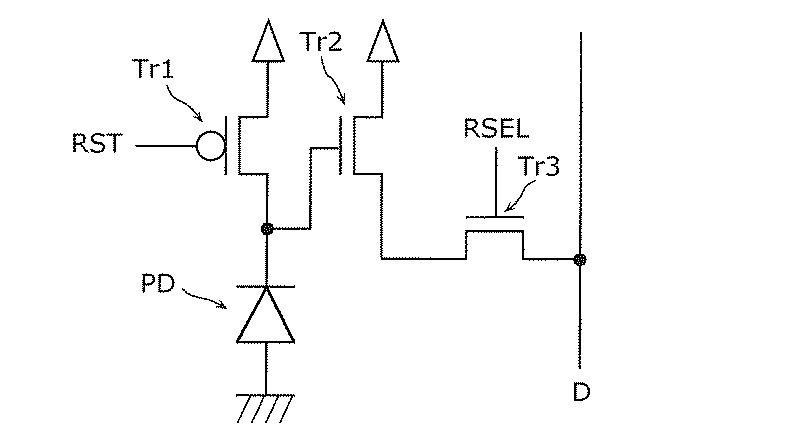
図4は、受光回路(PIX)301の一例を示す図である。受光回路(PIX)301は、一般的な3Tr型のAPS(Active Pixel Sensor)構造をとり、受光素子PDと、受光素子PDで発生した電荷を蓄積するコンデンサ(図示されず)と、前記コンデンサを一定電圧にリセットしておくためのリセットトランジスタTr1と、前記コンデンサに蓄積された電荷を増幅する増幅トランジスタTr2と、増幅後の信号を列信号線Dに出力する行選択トランジスタTr3とを備える。この受光回路301は、制御信号RSELで選択された場合に、輝度に応じた電圧を列信号線Dに出力する。
FIG. 4 is a diagram illustrating an example of the light receiving circuit (PIX) 301. The light receiving circuit (PIX) 301 has a general 3Tr APS (Active Pixel Sensor) structure, and includes a light receiving element PD, a capacitor (not shown) for accumulating charges generated in the light receiving element PD, and the capacitor. A reset transistor Tr1 for resetting to a constant voltage, an amplification transistor Tr2 for amplifying the charge accumulated in the capacitor, and a row selection transistor Tr3 for outputting the amplified signal to the column signal line D are provided. The
メモリ(MEM)302は1ビットのフラグを記憶するが、後述の処理部(PE)204との接続において、読み出しと書き込みを同一サイクルで行う必要があるため、2ポート構成のSRAM(static RAM)とする。 The memory (MEM) 302 stores a 1-bit flag. However, since it is necessary to perform reading and writing in the same cycle when connected to the processing unit (PE) 204 described later, a two-port SRAM (static RAM) And
作業用メモリ(WM)203は、1つの列につき3個配置される。作業用メモリWM(i,j)203, WM(i, j-1)203, WM(i, j+1)203は、「前記マトリクスの各列において処理対象となる画素を中心として列方向に連続する3個の値を保持するメモリ領域を有する」一例であり、その内訳は、処理部(PE)204が上から順に1行分ずつ後述の遷移処理を行う対象の画素の、遷移処理前のフラグを保持するWM(i, j)203と、その上の画素のフラグを保持するWM(i, j-1)203、およびその下の画素のフラグを保持するWM(i, j+1)203である。PE204の処理対象が次の行に移ると、それに伴ってWM(i, j-1)〜WM(i, j+1)の値は順に1つシフトされ、現在のWM(i, j-1)の値が直前のWM(i, j)の値に、現在のWM(i, j)の値が直前のWM(i, j+1)の値になる。現在のWM(i, j+1)の値は、新たにメモリ(MEM)から読み込む。処理部(PE)204が処理の対象とする画素のフラグの値は、処理対象の画素とその上下の3画素分のみであるため、作業用メモリ203はこのように3ビットのシフトレジスタの構成をとればよいことになる。
Three working memories (WM) 203 are arranged per column. The working memory WM (i, j) 203, WM (i, j-1) 203, WM (i, j + 1) 203 is "in the column direction with the pixel to be processed in each column of the matrix as the center. It has an example of a memory area that holds three consecutive values ”, and the breakdown is that before the transition process of the target pixel for which the processing unit (PE) 204 performs a later-described transition process for each row in order from the top. WM (i, j) 203 holding the flag of the above, WM (i, j-1) 203 holding the flag of the pixel above it, and WM (i, j + 1) holding the flag of the pixel below it ) 203. When the processing target of the
図5は、処理部(PE)204のより詳細な構成を示す図である。図5のように処理部(PE)204は、以下の4つの要素からなる。 FIG. 5 is a diagram showing a more detailed configuration of the processing unit (PE) 204. As shown in FIG. 5, the processing unit (PE) 204 includes the following four elements.
1.フラグ生成回路(FG)403
2.メモリアクセス制御回路(MC)401
3.拡大・収縮を行うためのオートマトン回路(A)404
4.X軸・Y軸への射影線生成回路(PG)402
1. Flag generation circuit (FG) 403
2. Memory access control circuit (MC) 401
3. Automaton circuit (A) 404 for expanding and contracting
4). Projection line generation circuit (PG) 402 for X axis and Y axis
1.のフラグ生成回路(FG)403は、前述の処理ステップ(1)と(3)において、順に選択される受光回路(PIX)301の出力電圧と閾値Vrefを電圧比較器によって比較し、瞳孔202あるいはプルキニエ像201を示すフラグを生成する。生成されたフラグは、順次対応するメモリ(MEM)302に保存される。
1. The flag generation circuit (FG) 403 compares the output voltage of the light receiving circuit (PIX) 301 selected in order with the threshold value Vref by the voltage comparator in the processing steps (1) and (3) described above. A flag indicating the
2.のメモリアクセス制御回路(MC)401は、請求項でいう「前記各列において同一行の画素が並行処理されるよう、クロックごとに各列で処理対象となる画素を行方向にシフトし、処理対象となる画素を中心として列方向に連続する3画素に対応する各前記メモリに保持されている値を読み出して、各前記メモリに対応する前記作業用メモリに書き込み、列方向に連続する前記3画素の中心に位置する画素に対応した前記メモリに、前記画像処理回路による画像処理の結果を書き込むメモリコントローラ」の一例である。メモリアクセス制御回路(MC)401は、前述の処理ステップ(2)、(4)、(5)において、順に処理対象となる行の1つ上の画素に対応するメモリ(MEM)302のフラグを読み出して作業メモリWM(i, j-1)203に格納するとともに、3.のオートマトン回路(A)404による処理結果Tを処理対象となっている画素PIX(i, j)に対応するメモリ(MEM)302に書き込む制御を行う。 2. The memory access control circuit (MC) 401 in the claims shifts the pixels to be processed in each column in the row direction every clock so that the pixels in the same row in each column are processed in parallel. A value held in each of the memories corresponding to three pixels continuous in the column direction with the target pixel as a center is read out, written in the working memory corresponding to each of the memories, and the three consecutive in the column direction It is an example of a “memory controller that writes the result of image processing by the image processing circuit to the memory corresponding to the pixel located at the center of the pixel”. The memory access control circuit (MC) 401 sequentially sets the flag of the memory (MEM) 302 corresponding to the pixel one pixel above in the row to be processed in the processing steps (2), (4), and (5) described above. 2. read out and store in work memory WM (i, j-1) 203; The processing result T by the automaton circuit (A) 404 is controlled to be written in the memory (MEM) 302 corresponding to the pixel PIX (i, j) to be processed.
3.のオートマトン回路(A)404は、「同一行の画素について並行して画像処理を行い、各前記作業用メモリに保持されている列方向に連続する3画素の値と、前記列の両側に隣接する列の各処理対象画素に対応する作業用メモリに保持されている値とを用いて画像処理を行う各列の前記画像処理回路」の一例である。オートマトン回路(A)404は、処理対象の画素PIX(i, j)及びその隣接4近傍画素PIX(i, j-1)、PIX(i, j+1)、PIX(i-1, j)、PIX(i+1, j)のフラグを格納する作業メモリWMの値を用いて拡大処理または収縮処理の遷移の結果Tを求める。例えば、オートマトン回路(A)404は、瞳孔に対する収縮処理の場合、中心画素と4近傍のすべてが“1”である場合に中心を“1”とする処理を行う。すなわち、中心と4近傍のうち1つでも“0”が含まれる場合には中心を“0”とする処理を行う。遷移の結果Tとは、すなわち、このような処理による中心のフラグの値である。図6は、図5に示したオートマトン回路(A)による収縮処理の遷移の一例を示す図である。図6(a)は、例えば、収縮処理における遷移の一例を示す図である。図6(a)では、フラグ生成回路(FG)によって2値化された値が適切なアドレスのメモリ(MEM)に書き込まれている。例えば、瞳孔の位置にはフラグ“1”が、それ以外の位置にはフラグ“0”が書き込まれている。図中、斜線で示す画素が瞳孔の位置である場合には、その画素に対応するメモリ(MEM)にフラグ“1”が書き込まれる。図6(a)の画像がN行M列である場合には、Nクロックで1画素幅の円の外周がフラグ“0”に反転される。図6(b)は、例えば、図6(a)に示した収縮処理の遷移の後、さらに遷移を繰り返した場合の一例を示す図である。図6(b)においても図6(a)の場合と同様に、Nクロックで、さらに1画素幅の円の外周がフラグ“0”に反転される。このようにして、収縮処理では、瞳孔などの円形画像が外周から順次、1画素の幅で削り取られ(“0”に反転していき)、徐々に縮小されることになる。図6(c)は、円形画像が外周から1画素の幅で順次、縮小され、円の中心となる最後の1画素が残った場合の一例を示す図である。同図に置いて円で囲まれた画素が消去点(中心)である。 3. The automaton circuit (A) 404 of “the image processing is performed in parallel on the pixels in the same row, and the values of three pixels consecutive in the column direction held in each of the working memories and adjacent to both sides of the column” 2 is an example of “the image processing circuit in each column that performs image processing using values held in a working memory corresponding to each processing target pixel in the column to be processed”. The automaton circuit (A) 404 includes a pixel PIX (i, j) to be processed and four neighboring pixels PIX (i, j-1), PIX (i, j + 1), PIX (i-1, j). The result T of the expansion process or the contraction process is obtained using the value of the working memory WM storing the flag of PIX (i + 1, j). For example, in the contraction process for the pupil, the automaton circuit (A) 404 performs a process of setting the center to “1” when all of the center pixel and the vicinity of 4 are “1”. In other words, if at least one of the center and four neighborhoods includes “0”, the center is set to “0”. The transition result T is the value of the central flag obtained by such processing. FIG. 6 is a diagram illustrating an example of a transition of contraction processing by the automaton circuit (A) illustrated in FIG. FIG. 6A is a diagram illustrating an example of transition in the contraction process, for example. In FIG. 6A, the value binarized by the flag generation circuit (FG) is written in the memory (MEM) at an appropriate address. For example, a flag “1” is written at the position of the pupil, and a flag “0” is written at the other positions. In the figure, when a pixel indicated by diagonal lines is the position of the pupil, a flag “1” is written in the memory (MEM) corresponding to the pixel. When the image of FIG. 6A has N rows and M columns, the circumference of a circle having a width of one pixel is inverted to the flag “0” in N clocks. FIG. 6B is a diagram illustrating an example in which the transition is further repeated after the transition of the contraction process illustrated in FIG. Also in FIG. 6B, as in the case of FIG. 6A, the outer periphery of the circle of 1 pixel width is inverted to the flag “0” in N clocks. In this way, in the contraction process, a circular image such as a pupil is sequentially scraped from the outer periphery with a width of one pixel (inverted to “0”) and gradually reduced. FIG. 6C is a diagram illustrating an example of a case where a circular image is sequentially reduced by a width of one pixel from the outer periphery, and the last one pixel remaining at the center of the circle remains. The pixel surrounded by a circle in the figure is the erase point (center).
4.の射影線生成回路(PG)402は、処理対象の画素のフラグの、X軸とY軸への射影像を生成する。これは、瞳孔の中心(“1”の画素)のX軸座標とY軸座標をそれぞれ算出する、つまり、“1”の位置(X軸座標とY軸座標)を検出するためである。図7(a)は、X軸への射影線生成回路(PG)の回路構成の一例を示す図である。X軸への射影像Pxは、図7(a)のように処理部(PE)204による1列分のすべての行の処理の期間の、オートマトン回路(A)404の出力Tの論理和を順にとることで求めることができる。図7(b)は、Y軸への射影線生成回路(PG)の回路構成の一例を示す図である。またY軸への射影像Pyは、図7(b)のようにすべての列の処理部(PE)204のオートマトン回路(A)404の出力T0, T1, T2,…TN-1の論理和を、順に接続されるORゲートによって求めることによって求められる。 4). The projection line generation circuit (PG) 402 generates a projection image of the flag of the pixel to be processed on the X axis and the Y axis. This is to calculate the X-axis coordinate and the Y-axis coordinate of the center of the pupil (pixel “1”), that is, to detect the position “1” (X-axis coordinate and Y-axis coordinate). FIG. 7A is a diagram illustrating an example of a circuit configuration of a projection line generation circuit (PG) for the X axis. The projected image Px on the X-axis is obtained by calculating the logical sum of the outputs T of the automaton circuit (A) 404 during the processing period of all the rows for one column by the processing unit (PE) 204 as shown in FIG. It can be obtained by taking in order. FIG. 7B is a diagram illustrating an example of a circuit configuration of a projecting line generation circuit (PG) for the Y axis. Further, as shown in FIG. 7B, the projected image Py on the Y axis is the logical sum of the outputs T0, T1, T2,... TN-1 of the automaton circuit (A) 404 of the processing units (PE) 204 of all the columns. Is obtained by an OR gate connected in sequence.
ここまでに述べた処理を順に行うために、受光回路(PIX)301の選択とフラグの生成、メモリ(MEM)の選択、拡大・収縮の処理、X軸・Y軸へのフラグの射影像からの消去点の検出と、その座標の生成をプライオリティ・エンコーダによって行う処理などを、全体の制御回路が制御する。 In order to perform the processing described so far in order, the selection of the light receiving circuit (PIX) 301 and the generation of the flag, the selection of the memory (MEM), the enlargement / contraction processing, the projection image of the flag to the X axis / Y axis The overall control circuit controls the detection of the erasing point and the process of generating the coordinates by the priority encoder.
以上のように、ここまでに述べた、視線検出のための列並列構成Vision Chipアーキテクチャの大まかな性能の見積もりを、動作速度と解像度の観点から述べる。 As described above, the rough estimation of the performance of the Vision Chip architecture for the line-parallel configuration for line-of-sight detection described so far will be described from the viewpoint of operation speed and resolution.
Vision Chipを構成する画素の行または列の数をNとする。処理ステップ数の大半を占める収縮処理では、処理部(PE)204のオートマトンの1回の遷移によって円形領域の両側1画素分収縮するため、最大でN/2回の遷移が必要となる。この収縮処理が瞳孔とプルキニエ像の両者に対して必要であるため、最大でN回の遷移が必要となることになる。また1列分の処理部PEの処理はN行に対して順に行われる。これから、1フレーム分の視線検出に必要な瞳孔・プルキニエ像の座標の生成を行うための収縮処理には、N×N回のオートマトンAの遷移が必要となることになる。したがって視線検出・追尾のフレームレートをFとすると、処理部PEの動作クロック周波数fは次式によって求められる。 Let N be the number of rows or columns of pixels that make up the Vision Chip. In the shrinking process that occupies most of the number of processing steps, one pixel on both sides of the circular region is shrunk by one transition of the automaton of the processing unit (PE) 204, so that a maximum of N / 2 transitions are required. Since this contraction process is necessary for both the pupil and the Purkinje image, a maximum of N transitions is required. Further, the processing of the processing unit PE for one column is sequentially performed on N rows. From this, N × N automaton A transitions are required for the contraction processing for generating the coordinates of the pupil and Purkinje image necessary for detecting the line of sight for one frame. Therefore, when the frame rate of the line-of-sight detection / tracking is F, the operation clock frequency f of the processing unit PE is obtained by the following equation.
サッケードの検出・追尾のためにはフレームレートF=500[Hz]程度が必要である(非特許文献4参照。)ので、VGA解像度(640×480画素)を実現するためには、N=480としてf=F×N×N =115[MHz]程度のクロック周波数で動作する必要がある。この動作速度は、近年の0.35μm程度あるいはそれより微細なCMOSプロセスによって十分実現可能な速度であると考えられる。 A frame rate of about F = 500 [Hz] is required for saccade detection / tracking (see Non-Patent Document 4). Therefore, in order to realize VGA resolution (640 × 480 pixels), N = 480 It is necessary to operate at a clock frequency of about f = F × N × N = 115 [MHz]. This operation speed is considered to be a speed that can be sufficiently realized by a CMOS process of about 0.35 μm or smaller in recent years.
1列分の回路の中で最も大きいのは処理部(PE)である。例えばCMPで利用できるaustriamicrosystems 0.35μm-optプロセスの論理ゲートのスタンダードセルの高さは20μm程度であり、このスタンダードセルを横に並べて処理部(PE)を作成すると、配線領域を含めて、1列分の幅はこの20μmよりもやや大きい25μm程度となると考えられる。またメモリMEMや受光回路PIXの幅は、この処理部PEの幅にあわせて設計することになる。したがってQVGA解像度(320×240画素)であれば全体の幅は25[μm]×240=6[mm]となり、この解像度は十分実現可能であると考えられる。またもう2世代微細な0.18μmプロセスを利用すれば、同一チップ面積でVGA解像度(640×480画素)も実現可能であると考えられる。このように、画像の抽象量を抽出するタイプのVision Chipとしては非常に高解像度なものが実現可能であると考えられる。 The largest of the circuits for one column is the processing unit (PE). For example, the height of the standard cell of the logic gate of the austriamicrosystems 0.35μm-opt process that can be used in CMP is about 20μm, and if this standard cell is arranged side by side to create a processing unit (PE), one line including the wiring area The width of the minute is considered to be about 25 μm, which is slightly larger than 20 μm. The widths of the memory MEM and the light receiving circuit PIX are designed in accordance with the width of the processing unit PE. Therefore, if the resolution is QVGA (320 × 240 pixels), the overall width is 25 [μm] × 240 = 6 [mm], and this resolution can be sufficiently realized. In addition, it is considered that VGA resolution (640 x 480 pixels) can be realized with the same chip area by using another generation 0.18 μm process. Thus, it is considered that a very high resolution chip can be realized as a type of Vision Chip that extracts an abstract amount of an image.
上記のように、本発明によれば、高解像度化のために列並列処理構成をとり、かつ、サッケード(急速眼球運動)の検出・追尾にも対応できる、高速な視線検出機能をもつVision Chipを得ることができた。大まかな見積もりの結果、十分実現可能な動作クロック周波数によってVGA解像度クラスの視線検出Vision Chipが実現可能である。 As described above, according to the present invention, a vision chip having a high-speed line-of-sight detection function that adopts a column parallel processing configuration for high resolution and can also cope with detection and tracking of saccades (rapid eye movement). Could get. As a result of rough estimation, it is possible to realize a visual line detection vision chip of the VGA resolution class with a sufficiently realizable operation clock frequency.
なお、上記実施の形態では、オートマトン回路(A)404によって瞳孔やプルキニエ像などの円の中心を検出する処理について説明したが、これは、画像処理の一例に過ぎず、本発明はこれに限定されない。本発明の撮像装置によれば、中心画素とその周辺4画素の値を用いて、例えば、画像の平滑化、エッジの検出などを行うことができる。例えば、画像の平滑化の場合には、周辺4画素の平均値を中心画素の値とすることにより実現することができる。また、エッジの検出の場合には、隣接する行間で行方向に対応する作業用メモリの値の差分を算出し、差分値が急激に変化した場合に行方向にエッジが存在することを判定することができる。列方向についても、隣接する列間で、列方向に対応する作業用メモリの値の差分を算出し、差分値が急激に変化した場合に列方向にエッジが存在することを判定することができる。これにより、車載カメラとして車線の検出などに用いることができるという効果がある。 In the above embodiment, the processing for detecting the center of a circle such as a pupil or a Purkinje image by the automaton circuit (A) 404 has been described. However, this is merely an example of image processing, and the present invention is not limited thereto. Not. According to the imaging apparatus of the present invention, for example, smoothing of an image, detection of an edge, and the like can be performed using the values of the center pixel and the surrounding four pixels. For example, in the case of smoothing an image, it can be realized by setting an average value of four peripheral pixels as the value of the central pixel. In the case of edge detection, the difference between the values in the working memory corresponding to the row direction between adjacent rows is calculated, and it is determined that an edge exists in the row direction when the difference value changes abruptly. be able to. Also in the column direction, it is possible to calculate the difference between the values in the working memory corresponding to the column direction between adjacent columns, and to determine that an edge exists in the column direction when the difference value changes abruptly. . Thereby, there exists an effect that it can use for the detection of a lane, etc. as a vehicle-mounted camera.
(実施の形態2)
上記実施の形態1では、サッケードを利用したユーザインタフェースのための撮像装置について説明したが、本実施の形態2では、車載カメラに搭載され、車輌の進行方向を横切る障害物を検出するための撮像装置について説明する。従来では車載カメラで取り込んだ画像をソフトウェアで処理する。しかし、従来のやり方ではフレームレートや処理速度が制限されるため、車輌が低速で走行している場合にしか障害物を検知することができないという問題がある。
(Embodiment 2)
In the first embodiment, the imaging device for the user interface using the saccade has been described. In the second embodiment, the imaging device is mounted on the in-vehicle camera and detects an obstacle crossing the traveling direction of the vehicle. The apparatus will be described. Conventionally, images captured by an in-vehicle camera are processed by software. However, since the frame rate and processing speed are limited in the conventional method, there is a problem that an obstacle can be detected only when the vehicle is traveling at a low speed.
図8は、オプティカル・フロー演算機能を備える列並列処理アーキテクチャである撮像装置800の1列分の回路構成を示す図である。
FIG. 8 is a diagram illustrating a circuit configuration for one column of the
撮像装置800は、方向別加算用メモリ(DM)801〜809、受光回路810、セレクタ(SEL)811、処理回路812、セレクタ(SEL)813、フレームメモリ(MEM)814、フレームメモリ(MEM)815、ブロック用メモリ(BM)816、ブロック用メモリ(BM)820、セレクタ(SEL)830及びセレクタ(SEL)831を備える。ブロック用メモリ820は、それぞれ1画素分の画素値を記憶するブロック用メモリ821〜829から構成される。ただし、ブロック用メモリ821〜823は、左隣の列に備えられる1列分のブロック用メモリであり、注目している当該列と左隣の列とで共有するメモリ資源である。また、ブロック用メモリ827〜829は、右隣の列に備えられる1列分のブロック用メモリであり、注目している当該列と右隣とで共有するメモリ資源である。
The
受光回路810は、行の各画素に相当する数のPDからなり、各PDは受光した光を、それぞれ1画素の画素値を表す電気量に変換する。
The
セレクタ813は、受光回路810で受光した各PDの画素値が、フレームごとに、各受光回路PDに対応付けてフレームメモリMEMに書き込まれるよう、フレームメモリ814、815の書き込みラインを選択する。フレームメモリ814とフレームメモリ815とには、フレームごとに新たな画像データが交互に書き込まれる。すなわち、セレクタ813は、フレームメモリ814に(t−1)番目のフレームが書き込まれ、フレームメモリ815にt番目のフレームが書き込まれ、当該フレーム間の処理が終了した場合には、(t−1)番目のフレームを書き込んだフレームメモリ814に次のフレームである(t+1)番目のフレームを書き込むように制御される。フレームメモリ815にt番目のフレームが書き込まれているときに、フレームメモリ814に(t+1)番目のフレームが書き込まれると、セレクタ830はフレームメモリ815からt番目のフレームの画素値がブロック用メモリ816に読み出されるようにフレームメモリ815の読み出し線を選択する。また、セレクタ831は、フレームメモリ814に(t+1)番目のフレームが書き込まれると、ブロック用メモリ824〜826に、フレームメモリ814から(t+1)番目のフレームの画素値が読み出されるようにフレームメモリ814の読み出し線を選択する。
The
フレームメモリ814、815は、「前記複数の受光回路から構成される現在のフレームと直前のフレームにおける前記電気量の値を保持する記憶容量を有する前記メモリ」の一例である。
The
フレームメモリ814は、行の各画素における画素値を記憶するための行の数に等しいメモリMEMからなり、直前のフレームである(t−1)番目のフレームの1列分の画素値を記憶する。
The
フレームメモリ815は、フレームメモリ814と同数のメモリMEMからなり、現在のフレームであるt番目のフレームの1列分の画素値を記憶する。
The
ブロック用メモリ816は、フレームメモリ814の1つのMEMから読み出された、例えば、3行3列のブロックの中央の1画素の画素値を記憶する。
The block memory 816 stores, for example, the pixel value of one pixel at the center of a 3 × 3 block read from one MEM of the
ブロック用メモリ820は、t番目のフレームの例えば、3行3列のブロックの各画素値を記憶する3行3列のブロック用メモリBM821〜829から構成される。このうち、ブロック用メモリ824〜826は、受光回路810で受光された当該列のt番目フレームのうち、3行分の画素値を記憶する。ブロック用メモリ825は、t番目のフレームにおいて、ブロック用メモリ816に画素値が記憶されている画素と同じ位置の画素値を記憶する。ブロック用メモリ821〜823は、それぞれ図示しない左隣の列のフレームメモリMEMに記憶されている左隣の列のt番目のフレームのうち、ブロック用メモリ824〜826に画素値が記憶されている各画素の左隣の画素の画素値を記憶する。ブロック用メモリ827〜829は、それぞれ図示しない右隣の列のフレームメモリMEMに記憶されている右隣の列のt番目のフレームのうち、ブロック用メモリ824〜826のそれぞれに画素値が記憶されている各画素の右隣の画素の画素値を記憶する。
The
すなわち、ブロック用メモリ821は、t番目のフレームで、ブロック用メモリ825が画素値を記憶している画素(=3行3列のブロックの中央の画素)に対して左上に位置する画素の画素値を記憶する。ブロック用メモリ822は、t番目のフレームで、3行3列のブロックの中央の画素に対して左に位置する画素の画素値を記憶する。ブロック用メモリ823は、t番目のフレームで、3行3列のブロックの中央の画素に対して左下に位置する画素の画素値を記憶する。
That is, the
また、ブロック用メモリ824は、3行3列のブロックの中央の画素に対して真上に位置する画素の画素値を記憶する。ブロック用メモリ825は、t番目のフレームで、3行3列のブロックの中央の画素の画素値を記憶する。ブロック用メモリBM826は、t番目のフレームで、3行3列のブロックの中央の画素に対して真下に位置する画素の画素値を記憶する。 The block memory 824 stores the pixel value of the pixel located directly above the center pixel of the 3 × 3 block. The block memory 825 stores the pixel value of the center pixel of the 3 × 3 block in the t-th frame. The block memory BM826 stores the pixel value of the pixel located directly below the center pixel of the 3 × 3 block in the t-th frame.
すなわち、ブロック用メモリ827は、t番目のフレームで、3行3列のブロックの中央の画素に対して右上に位置する画素の画素値を記憶する。ブロック用メモリBM828は、t番目のフレームで、3行3列のブロックの中央の画素に対して右に位置する画素の画素値を記憶する。ブロック用メモリ829は、t番目のフレームで、3行3列のブロックの中央の画素に対して右下に位置する画素の画素値を記憶する。
That is, the
処理回路812は、「前記方向別加算用メモリを作業用メモリとして用いながら、前記現在及び直前のフレームにおける電気量の値から、ブロックマッチング法によってオプティカルフローを算出する前記画像処理回路」および「オプティカルフローの方向を示す8方向または9方向について、N行N列(ただし、Nは3以上の自然数)の画素からなるブロックによるブロックマッチングを行うことで、前記画像の動きを示す方向として、前記8方向または前記9方向の1つを特定し、特定した方向を示す値を出力する前記画像処理回路」の一例である。この処理回路812は、受光回路810の列ごとに備えられ、隣接する列のフレームメモリ及びブロック用メモリなどから得られる値を参照して中心画素と隣接8画素とからなる画素のオプティカル・フロー演算を行う。
The
セレクタ811は、処理回路812から9ライン並列で入力される差分絶対値を加算するための方向別加算用メモリ801〜809の行を選択する。
The
方向別加算用メモリ801〜809は、「前記現在及び直前のフレームでの画像の動きを示すオプティカルフローを算出するための一時的な値を保持するための方向別加算用メモリ」の一例であり、静止位置も含めた9方向の探索を並列処理で行うために、1行につき9個の加算用メモリを3行分備える。各行の加算用メモリは、それぞれ上下のブロックの方向別の差分絶対値の和を記憶する。また、方向別加算用メモリ801は、ブロック用メモリ816に画素値が記憶されている直前フレームの画素値と、現在のフレームで直前フレームの画素と同位置にある画素の画素値との差分の絶対値を記憶し、順次加算するための記憶容量を有するメモリである。各行の方向別加算用メモリ802は、直前フレームの画素の画素値と、その右方向にある現在のフレーム画素の画素値との差分の絶対値を加算するための記憶容量を有するメモリである。
The direction-
以上のように、撮像素子と処理回路とを結合することにより、高解像度でかつ高速な画像処理を実現することができるので、車輌と障害物とが両方とも高速で移動している場合でも、障害物を検知することが可能になる。 As described above, by combining the image sensor and the processing circuit, high-resolution and high-speed image processing can be realized, so even when both the vehicle and the obstacle are moving at high speed, Obstacles can be detected.
図9は、車輌と障害物とが両方とも所定の速度で移動している場合に、衝突前に停止できるよう障害物を検出するために必要な撮像装置800のフレームレートを算出するための図である。
FIG. 9 is a diagram for calculating a frame rate of the
例えば、60km/hで走行中の車輌が、40m前方を25km/hで横切る自転車を検知する状況を想定する。この場合、車輌が自転車を検知してから停止するまでに要する停止距離は、空走距離17m+制動距離27m=44mである。この場合、車輌が停止するまでの時間は、2.64秒であり、車輌が停止するまでの2.64秒間で25km/hの自転車は約20m進む。車載カメラの撮影範囲を車輌の前方44mにおいて20mの幅であるとすると、撮像装置800に必要なフレームレートは200fps(frame per second)である。
For example, a situation is assumed in which a vehicle traveling at 60 km / h detects a bicycle crossing 40 m ahead at 25 km / h. In this case, the stop distance required for the vehicle to stop after detecting the bicycle is the idling distance 17 m + braking distance 27 m = 44 m. In this case, the time until the vehicle stops is 2.64 seconds, and a 25 km / h bicycle travels about 20 meters in 2.64 seconds until the vehicle stops. Assuming that the shooting range of the in-vehicle camera is 20 m wide at 44 m ahead of the vehicle, the frame rate required for the
図10は、撮像装置800のオプティカル・フロー演算のために必要なブロックサイズ及びフレームレートを算出するための説明図である。
FIG. 10 is an explanatory diagram for calculating a block size and a frame rate necessary for the optical flow calculation of the
撮像装置800の撮影画像をVGA(640×480画素)で考える。図に示すように、1画素の大きさは、20m÷640=31.25(mm/pixel)となる。3×3画素のブロックの大きさは、94(mm)×94(mm)である。
A captured image of the
撮像装置800では、フレームレートが200fpsの場合、5msに1回走査を行う。また、自転車は5msで34.7mm進む。従って、自転車はフレームレートが200fpsのとき、1走査で約1画素画面を動くことになる。従って、フレームレートを200fpsとした場合、静止も含めて周囲9方向、静止を含めなければ周囲8方向に1画素分だけずらしたブロックを探索すればよいことになる。
In the
従来、動き検出の方法としては、勾配法やブロックマッチング法が知られている。しかし、勾配法では、対応点の検索を行う必要がないために計算量は少なくて済むが、輝度値が急激に変化するところではオプティカル・フローの誤差が大きいこと、雑音に弱いというデメリットがある。 Conventionally, gradient methods and block matching methods are known as motion detection methods. However, the gradient method does not need to search for corresponding points, so the amount of calculation is small. However, there are disadvantages in that the optical flow error is large and the noise is weak when the luminance value changes rapidly. .
これに対し、ブロックマッチング法では、探索範囲を制限すればある程度低減することができるが、計算時間が膨大で、拡大・縮小・回転運動に弱いという問題がある。しかしながら、ブロックマッチング法では、計算が簡単であり、輝度値の急激に変化するところでもオプティカル・フローの誤差が小さく、雑音に強いというメリットがある。 On the other hand, the block matching method can be reduced to some extent if the search range is limited, but has a problem that the calculation time is enormous and it is vulnerable to enlargement / reduction / rotation. However, the block matching method has a merit that the calculation is simple, the optical flow error is small even in a place where the luminance value changes rapidly, and it is resistant to noise.
従って、本発明ではブロックマッチング法を用いてオプティカル・フロー演算を行う。
図11は、オプティカル・フローを説明する図である。オプティカル・フローとは、動画像における連続したフレーム間での濃度分布の移動をベクトルで表したものをいう。図11(a)に示すように、前フレームで任意の位置にあったブロックが、現フレームのどの位置に移動したかを示すものである。具体的には、前フレームにあったブロックが、現フレーム上で元の位置からどの方向にどれだけ移動したかをベクトルで示したものである。例えば、図11(b)では、前フレームのブロックの中心を始点として、現フレームのブロックの中心までの移動方向及び移動量をベクトルで示している。
Therefore, in the present invention, the optical flow calculation is performed using the block matching method.
FIG. 11 is a diagram for explaining the optical flow. The optical flow is a vector that represents the movement of the density distribution between successive frames in a moving image. As shown in FIG. 11 (a), it indicates to which position in the current frame a block that was in an arbitrary position in the previous frame has moved. Specifically, the vector indicates how much the block in the previous frame has moved in which direction from the original position on the current frame. For example, in FIG. 11B, the moving direction and the moving amount to the center of the block of the current frame are represented by vectors, starting from the center of the block of the previous frame.
図12は、オプティカル・フローの算出方法を説明する図である。ここでは、ブロックマッチング法を用いたオプティカル・フロー算出方法について説明する。図12(a)は、(t−1)番目のフレーム画像を示している。図12(b)は、t番目のフレーム画像を示している。ブロックマッチング法では、t番目のフレームの前フレームである(t−1)番目の画像中の任意のブロックを参照ブロックとする。そして、図12(b)のように、現在のフレームであるt番目のフレームにおいて、同じパターンの画像を示すブロックを探索する方法である。前フレームのブロックと同じ画像を示すブロックが現フレームで見つかれば、前フレームのブロックが現フレームにおいて見つかった位置まで移動したものとして、移動量をベクトルであらわすことができる。 FIG. 12 is a diagram for explaining an optical flow calculation method. Here, an optical flow calculation method using the block matching method will be described. FIG. 12A shows the (t−1) th frame image. FIG. 12B shows the t-th frame image. In the block matching method, an arbitrary block in the (t−1) th image that is the previous frame of the tth frame is used as a reference block. Then, as shown in FIG. 12B, in the t-th frame, which is the current frame, a method of searching for a block indicating the same pattern image is performed. If a block showing the same image as the block of the previous frame is found in the current frame, the movement amount can be expressed as a vector, assuming that the block of the previous frame has moved to the position found in the current frame.
図13は、本実施の形態のブロックマッチング法について説明する図である。本実施の形態2では、対象が1フレーム間で1画素しか動かないと仮定して、図13(a)に示すように、参照ブロックから周囲8方向にそれぞれ1画素ずらした範囲を探索するものとする。図13(a)では、破線で囲んだ3×3画素のブロックを参照ブロックとして、現フレームにおけるブロックの探索範囲を、前フレームにおける参照ブロックから周囲8方向にそれぞれ1画素ずらした5×5画素のブロック1201の範囲を探索する。
FIG. 13 is a diagram for explaining the block matching method of the present embodiment. In the second embodiment, assuming that the target moves only one pixel in one frame, as shown in FIG. 13 (a), a range that is shifted by one pixel from the reference block in each of the eight surrounding directions is searched. And In FIG. 13A, a block of 3 × 3 pixels surrounded by a broken line is used as a reference block, and the search range of the block in the current frame is shifted by 1 pixel in each of the surrounding 8 directions from the reference block in the previous frame. The range of the
図13(b)は、(t−1)番目のフレームにある参照ブロック1202と、t番目のフレームの探索範囲内にある同じ大きさのブロック1203を示す図である。t番目のフレームの探索範囲内で、参照ブロックがどの位置に移動したかを判定するには、参照ブロックと同じ大きさのブロックとで、同じ位置にある画素同士の輝度の差分の絶対値の総和をとる。すなわち、図13(b)の参照ブロック1202とt番目のフレームにあるブロック1203とで、同じ位置にある画素同士、すなわち、画素A1と画素B1、画素A2と画素B2、画素A3と画素B3、・・・、画素A9と画素B9のそれぞれの輝度の差分の絶対値の総和
そして、ブロックマッチング法では、上記の9回の計算により算出された9個の差分絶対値の総和の中で、その総和が最小となるブロックに参照フレーム1202が動いたものと判断する。そして、参照ブロック1202から、輝度の差分の絶対値の総和が最小となるブロックへの方向を動きベクトルとする。
In the block matching method, it is determined that the
上記の演算を本発明の撮像装置800では、列並列処理で行う。すなわち、処理回路812は、図8に示したように、画素の1列に1つ備えられているので、ブロックマッチングの処理を列ごとに行う。そして、行単位で上から順に処理を行う。
The above calculation is performed by column parallel processing in the
この場合、画素単位に処理回路を備えて画素単位で行う「画素並列処理」と比較すると、処理速度が画素並列処理よりも少し遅くなるが、画素並列処理では画素及び処理回路が大きくなるという弊害があるのに対し、列並列処理では撮像部と処理回路とを分離することが可能になるので画素数を増やしても処理回路はそれほど大きくならないというメリットがある。 In this case, the processing speed is slightly slower than the pixel parallel processing compared to the “pixel parallel processing” that includes a processing circuit for each pixel and is performed on a pixel basis. However, the pixel parallel processing increases the size of the pixel and the processing circuit. On the other hand, in the column parallel processing, since the imaging unit and the processing circuit can be separated, there is an advantage that the processing circuit does not become so large even if the number of pixels is increased.
図14は、列並列処理のブロックマッチングの手順の一例を示す図である。図14(a)は、同図左で(t−1)番目のフレームの参照ブロックを構成する1画素を示し、同図右でその画素位置から周囲8方向に1画素ずつずれた位置にある画素を含んで構成されるt番目フレーム上のブロックを示している。図14(b)は、図14(a)左で示した(t−1)番目のフレームの画素から一行下の1画素を示し、同図右でその画素位置から周囲8方向に1画素ずつずれた位置にある画素を含んで構成されるt番目フレーム上のブロックを示している。図14(c)は、図14(b)左で示した(t−1)番目のフレームの画素からさらに一行下の1画素を示し、同図右でその画素位置から周囲8方向に1画素ずつずれた位置にある画素を含んで構成されるt番目フレーム上のブロックを示している。図14(d)は、中央の列の処理回路が、図14(a)、(b)、(c)の順で、(t−1)番目のフレーム上の画素と、各図左に示したブロック内の各画素との画素値の差分絶対値の総和を算出することを示している。 FIG. 14 is a diagram illustrating an example of a block matching procedure for column parallel processing. FIG. 14A shows one pixel constituting the reference block of the (t−1) -th frame on the left side of the figure, and is located on the right side of the figure at a position shifted by one pixel from the pixel position in the surrounding eight directions. A block on the t-th frame including pixels is shown. FIG. 14B shows one pixel one row below the pixel of the (t−1) -th frame shown on the left of FIG. 14A, and one pixel at a time in the eight directions from the pixel position on the right of FIG. A block on the t-th frame configured to include a pixel at a shifted position is shown. FIG. 14C shows one pixel further down one row from the pixel in the (t−1) -th frame shown on the left in FIG. 14B, and one pixel on the right in the figure from the pixel position to the surrounding eight directions. A block on the t-th frame configured to include pixels at different positions is shown. FIG. 14 (d) shows the processing circuit in the center column in the order of FIGS. 14 (a), (b) and (c), with the pixels on the (t-1) th frame and the left side of each figure. In other words, the sum of absolute differences of pixel values with respect to each pixel in the block is calculated.
図14(d)に示すように、ブロックマッチングの演算処理を行う列は中央の列の処理回路812である。図では説明しないが、この列と並行してそれぞれ隣接するすべての列に備えられる処理回路で同じ演算が同時に実行されていることが前提である。図8に示した方向別加算用メモリ801〜809は3行分あり、1行目の9方向の方向別加算用メモリ801〜809は、それぞれ、図14(a)の画素に対する方向別の差分絶対値を記憶する。2行目の9方向の方向別加算用メモリ801〜809は、それぞれ、図14(b)の画素に対する方向別の差分絶対値を記憶する。3行目の9方向の方向別加算用メモリ801〜809は、それぞれ、図14(c)の画素に対する方向別の差分絶対値を記憶する。
As shown in FIG. 14D, the column on which the block matching calculation process is performed is the
これらに記憶されている3行分の方向別加算用メモリ801〜809に、右隣の列と左隣の列の方向別加算用メモリ801〜809の方向別差分絶対値を加算し、方向別で差分の絶対値の総和が最小となる方向を算出することによって、3行3列のブロックのブロックマッチングを行うことができる。
The direction-specific difference absolute values of the direction-
図14(a)に示すように、処理回路812は、まず、同図左に示す画素と、同図右に示すブロックを構成する9画素とのそれぞれの画素値の差分絶対値の総和を算出する。図14(a)、(b)及び(c)の左隣の列、右隣の列の各画素の画素値は、いずれも、隣の列と共有される。
As shown in FIG. 14A, the
各処理回路812が実行する1列分の演算回数は、画素数X×Y、ブロックサイズN×Nとすると、
差分絶対値の計算回数 N2×Y回
方向別加算用メモリ801〜809への加算回数 9N2×Y回
最小値を算出する回数 Y回
となる。これに対し、動作可能なクロック周波数f[Hz]は、F[fps]をフレームレートとして
f=F×〔{N2×Y}+{9N2×Y}+Y〕
=F×Y×10N2[Hz]
となる。ここで、例えば、F=200[fps]、Y=480、N=3のとき、
f=200×480×10×32
≒8[MHz]
となり、一般的なCMOS回路で実現可能であることが分かる。
Assuming that the number of operations for one column executed by each
Number of absolute difference calculations N 2 × Y times Number of additions to the direction-
= F x Y x 10N 2 [Hz]
It becomes. Here, for example, when F = 200 [fps], Y = 480, and N = 3,
f = 200 × 480 × 10 × 3 2
≒ 8 [MHz]
Thus, it can be seen that it can be realized with a general CMOS circuit.
なお、上記の説明では、フレーム間で静止している画素同士の画素値の差分の絶対値の総和も計算したが、直前フレームと現フレームとで同位置にある画素同士の画素値についての差分絶対値の計算を省略するとしてもよい。この場合、方向別加算用メモリの数も8個ですみ、探索方向の計算も8個で済むので、計算量もメモリ資源もともに節約することができる。 In the above description, the sum of absolute values of pixel value differences between pixels that are stationary between frames is also calculated. However, the difference between the pixel values of pixels at the same position in the previous frame and the current frame is also calculated. The calculation of the absolute value may be omitted. In this case, only eight direction-specific addition memories are required and only eight search directions are calculated, so that both the calculation amount and the memory resources can be saved.
静止位置にある画素のマッチングを省略する場合には、各処理回路812が実行する1列分の演算回数は、画素数X×Y、ブロックサイズN×Nとすると、
差分絶対値の計算回数 (N2−1)×Y回
方向別加算用メモリ801〜809への加算回数 8N2×Y回
最小値を算出する回数 Y回
となる。ここで、最小値を算出する場合に、7個の2値コンパレータを用いることによって、1クロックで一度に8方向の差分絶対値の総和の最小値を得ることができる。また、動作可能なクロック周波数f[Hz]は、F[fps]をフレームレートとして
f=F×〔{(N2−1)×Y}+{8N2×Y}+Y〕
=F×Y×9N2[Hz]
となる。ここで、例えば、F=200[fps]、Y=480、N=3のとき、クロック周波数f[Hz]は、
f=200×480×9×32
≒7[MHz]
ですみ、一般的なCMOS回路で十分実現可能となる。
When the matching of the pixels at the stationary position is omitted, the number of operations for one column executed by each
Number of absolute difference calculations (N 2 −1) × Y times Number of additions to the direction-
= F x Y x 9N 2 [Hz]
It becomes. Here, for example, when F = 200 [fps], Y = 480, and N = 3, the clock frequency f [Hz] is
f = 200 × 480 × 9 × 3 2
≒ 7 [MHz]
In fact, a general CMOS circuit can be sufficiently realized.
また、ここでは、3行3列の画素からなるブロックを探索の単位としたが、探索精度をより高めるために、例えば、5行5列の画素からなるブロックを探索の単位としてブロックマッチングを行うとしてもよい。この場合、ブロック用メモリが左右に一列ずつ増えることになるが、その分、処理精度か高くなる。また、それ以上の画素からなるブロック、例えば、N行N列(ただしNは自然数)の画素からなるブロックを探索の単位としてブロックマッチングを行うとしてもよい。 In addition, here, a block consisting of pixels of 3 rows and 3 columns is used as a search unit. However, in order to further improve the search accuracy, for example, block matching is performed using a block consisting of pixels of 5 rows and 5 columns as a search unit. It is good. In this case, the block memory increases by one row on the left and right, but the processing accuracy is increased accordingly. In addition, block matching may be performed using a block including more pixels, for example, a block including N rows and N columns (where N is a natural number) as a search unit.
図15は、実際の画像を用いたシミュレーションの一例を示す図である。同図では、上記撮像装置800で実際に動き検出が可能かどうかを調べるために、グレースケールのVGA静止画像を背景とした。各ブロックごとにどの方向へ動いたかを以下のように出力する。例えば、真下に動いた場合には、
同図では、ハッチングで示す直方体の上下の境界で、上記の出力が得られ、下方への動きが確認できた。この場合には、ハッチングで示す直方体は、実際の画像では黒一色である。このような場合には、背景の動きは検出されないので、階調が低くても検出可能である。 In the figure, the above output was obtained at the upper and lower boundaries of the rectangular parallelepiped indicated by hatching, and the downward movement was confirmed. In this case, the rectangular parallelepiped indicated by hatching is black in the actual image. In such a case, since the background motion is not detected, it can be detected even if the gradation is low.
図16は、実際の画像を用いたシミュレーションの他の例を示す図である。同図においてハッチングで示す直方体は、グレーである。この場合でも、直方体の左右の境界で動きが以下のように出力され、
なお、上記実施の形態2では、フレームメモリ814とフレームメモリ815とに、新たなフレームの画像データを交互に書き込むよう制御したが、本発明はこれに限定されない。例えば、フレームメモリ814には、常にフレームメモリ815に書き込まれるフレームに対して直前のフレームが書き込まれるように制御するとしてもよい。この場合、セレクタ830及びセレクタ831は不要になり、ブロック用メモリ816には常にフレームメモリ814の画素値を記憶させ、ブロック用メモリ824〜826には常にフレームメモリ815から読み出された画素値を記憶させるようにしてもよい。
In the second embodiment, control is performed so that image data of new frames are alternately written in the
なお、ブロック図(図1、図3、図5及び図8など)のブロックは典型的には集積回路であるLSIとして実現され、個別に1チップ化されても良いし、一部又は全てを含むように1チップ化されても良い。例えばメモリ以外の機能ブロックが1チップ化されても良い。 Note that the blocks in the block diagrams (FIGS. 1, 3, 5, and 8) are typically realized as LSIs that are integrated circuits, and may be individually integrated into one chip, or part or all of them. It may be made into one chip so as to include it. For example, the functional blocks other than the memory may be integrated into one chip.
本発明は、サッケードを利用したユーザインタフェース等に適用できる。また、本発明は、撮影した画像に対して高速に高解像度で画像の平滑化及びエッジの検出を行う撮像装置に適用できる。さらに、本発明は車載用の移動障害物検知装置に適用できる。 The present invention can be applied to a user interface using a saccade. The present invention can also be applied to an imaging apparatus that performs high-speed and high-resolution image smoothing and edge detection on a captured image. Furthermore, the present invention can be applied to an on-vehicle moving obstacle detection device.
101 受光回路(PIX)
102 メモリ(MEM)
103 処理部
201 プルキニエ像
202 瞳孔
203 作業用メモリWM(i, j)、WM(i, j-1)、WM(i, j+1)
204 処理部(PE)
205 作業メモリWM(i-1, j), WM(i+1, j)
301 受光回路(PIX)
302 メモリ(MEM)
401 メモリアクセス制御回路(MC)
402 射影線生成回路(PG)
403 フラグ生成回路(FG)
404 オートマトン回路(A)
800 撮像装置
801〜809 方向別加算用メモリ(DM)
810 受光回路
811、813、830、831 セレクタ(SEL)
812 処理回路
814、815 フレームメモリ(MEM)
816、820 ブロック用メモリ(BM)
101 Light receiving circuit (PIX)
102 Memory (MEM)
103
204 Processing unit (PE)
205 Working memory WM (i-1, j), WM (i + 1, j)
301 Light receiving circuit (PIX)
302 Memory (MEM)
401 Memory access control circuit (MC)
402 Projection line generation circuit (PG)
403 Flag generation circuit (FG)
404 Automaton circuit (A)
800 Imaging device 801-809 Addition memory for each direction (DM)
810
812
816, 820 block memory (BM)
Claims (7)
マトリクス状に配置され、それぞれが受光した光の量を電気量に変換する画素である複数の受光回路と、
各前記受光回路で得られた電気量の値を、各前記受光回路に対応付けて保持するメモリと、
前記マトリクスの列ごとに備えられる処理部とを備え、
前記処理部は、
前記メモリに保持されているうち少なくとも一部の列方向に連続する複数個の値を保持するための作業用メモリと、
前記作業用メモリに保持されている値を用いて、所定の画像処理を行う画像処理回路と
を備えることを特徴とする撮像装置。 An imaging device having an image processing function,
A plurality of light receiving circuits arranged in a matrix and each pixel being a pixel that converts the amount of received light into an electrical quantity;
A memory that holds the value of the electric quantity obtained by each of the light receiving circuits in association with each of the light receiving circuits;
A processing unit provided for each column of the matrix,
The processor is
A working memory for holding a plurality of values that are continuous in at least some of the column directions held in the memory;
An image processing apparatus comprising: an image processing circuit that performs predetermined image processing using a value held in the working memory.
前記撮像装置は、さらに、
前記各列において同一行の画素が並行処理されるよう、クロックごとに各列で処理対象となる画素を行方向にシフトし、処理対象となる画素を中心として列方向に連続する3画素に対応する各前記メモリに保持されている値を読み出して、各前記メモリに対応する前記作業用メモリに書き込むメモリコントローラを備え、
各列の前記画像処理回路は、同一行の画素について並行して画像処理を行い、各前記作業用メモリに保持されている列方向に連続する3画素の値と、前記列の両側に隣接する列の各処理対象画素に対応する作業用メモリに保持されている値とを用いて画像処理を行い、
前記メモリコントローラは、列方向に連続する前記3画素の中心に位置する画素に対応した前記メモリに、前記画像処理回路による画像処理の結果を書き込む
ことを特徴とする請求項1記載の撮像装置。 The working memory has a memory area that holds three values that are continuous in the column direction around the pixel to be processed in each column of the matrix,
The imaging device further includes:
The pixels to be processed in each column are shifted in the row direction at each clock so that pixels in the same row are processed in parallel in each column, and three pixels that are continuous in the column direction centering on the pixel to be processed are supported. A memory controller that reads a value held in each memory and writes the value to the working memory corresponding to each memory;
The image processing circuit in each column performs image processing on the pixels in the same row in parallel, and is adjacent to both sides of the column and the value of three pixels continuous in the column direction held in each working memory. Image processing is performed using values held in the working memory corresponding to each processing target pixel in the column,
The imaging apparatus according to claim 1, wherein the memory controller writes an image processing result by the image processing circuit in the memory corresponding to a pixel located at a center of the three pixels continuous in a column direction.
前記受光回路で得られた電気量の値と予め定められた値とを比較することによって、比較結果を示すフラグを生成するフラグ生成部と、
前記フラグを用いて画像の拡大又は縮小処理の遷移を求めるオートマトン回路と、
前記オートマトン回路によって求められたフラグを用いて、前記画像の前記受光回路におけるX軸座標及びY軸座標を算出する射影線生成回路とを備える
ことを特徴とする請求項2記載の撮像装置。 The image processing circuit includes:
A flag generation unit that generates a flag indicating a comparison result by comparing the value of the amount of electricity obtained by the light receiving circuit with a predetermined value;
An automaton circuit for obtaining a transition of an image enlargement or reduction process using the flag;
The imaging apparatus according to claim 2, further comprising: a projection line generation circuit that calculates an X-axis coordinate and a Y-axis coordinate in the light receiving circuit of the image using a flag obtained by the automaton circuit.
前記オートマトン回路は、前記瞳孔又はプルキニエ像の中心位置を示す1個の画素に対応するフラグだけが1又は0となるまで、収縮処理の遷移を求める
ことを特徴とする請求項3記載の撮像装置。 The flag generation unit generates the flag by comparing the value of the electric quantity obtained by the light receiving circuit with a predetermined value for specifying a pupil or a Purkinje image,
The imaging apparatus according to claim 3, wherein the automaton circuit obtains a transition of contraction processing until only a flag corresponding to one pixel indicating a center position of the pupil or a Purkinje image becomes 1 or 0. .
前記撮像装置は、さらに、前記現在及び直前のフレームでの画像の動きを示すオプティカルフローを算出するための一時的な値を保持するための方向別加算用メモリを有し、
前記画像処理回路は、前記方向別加算用メモリを作業用メモリとして用いながら、前記現在及び直前のフレームにおける電気量の値から、ブロックマッチング法によってオプティカルフローを算出する
ことを特徴とする請求項2記載の撮像装置。 The memory has a storage capacity for holding the value of the amount of electricity in the current frame and the immediately preceding frame composed of the plurality of light receiving circuits,
The imaging apparatus further includes a direction-specific addition memory for holding a temporary value for calculating an optical flow indicating the movement of the image in the current and previous frames,
The image processing circuit calculates an optical flow by a block matching method from values of electricity in the current and immediately preceding frames while using the direction-specific addition memory as a working memory. The imaging device described.
ことを特徴とする請求項5記載の撮像装置。 The image processing circuit performs block matching with a block composed of pixels of N rows and N columns (where N is a natural number of 3 or more) in 8 directions or 9 directions indicating the direction of optical flow, thereby moving the image The imaging apparatus according to claim 5, wherein one of the eight directions or the nine directions is specified as a direction indicating, and a value indicating the specified direction is output.
マトリクス状に配置され、それぞれが受光した光の量を電気量に変換する画素である複数の受光回路と、
各前記受光回路で得られた電気量の値を、各前記受光回路に対応付けて保持するメモリと、
前記マトリクスの列ごとに備えられる処理部とを備え、
前記処理部は、
前記メモリに保持されているうち少なくとも一部の列方向に連続する複数個の値を保持するための作業用メモリと、
前記作業用メモリに保持されている値を用いて、所定の画像処理を行う画像処理回路と
を備えることを特徴とする集積回路。 An integrated circuit for mounting an imaging device having an image processing function,
A plurality of light receiving circuits arranged in a matrix and each pixel being a pixel that converts the amount of received light into an electrical quantity;
A memory that holds the value of the electric quantity obtained by each of the light receiving circuits in association with each of the light receiving circuits;
A processing unit provided for each column of the matrix,
The processor is
A working memory for holding a plurality of values that are continuous in at least some of the column directions held in the memory;
An integrated circuit comprising: an image processing circuit that performs predetermined image processing using a value held in the working memory.
Priority Applications (1)
| Application Number | Priority Date | Filing Date | Title |
|---|---|---|---|
| JP2008013121A JP2008206143A (en) | 2007-01-23 | 2008-01-23 | Imaging device having image processing function |
Applications Claiming Priority (2)
| Application Number | Priority Date | Filing Date | Title |
|---|---|---|---|
| JP2007013120 | 2007-01-23 | ||
| JP2008013121A JP2008206143A (en) | 2007-01-23 | 2008-01-23 | Imaging device having image processing function |
Publications (1)
| Publication Number | Publication Date |
|---|---|
| JP2008206143A true JP2008206143A (en) | 2008-09-04 |
Family
ID=39783092
Family Applications (1)
| Application Number | Title | Priority Date | Filing Date |
|---|---|---|---|
| JP2008013121A Pending JP2008206143A (en) | 2007-01-23 | 2008-01-23 | Imaging device having image processing function |
Country Status (1)
| Country | Link |
|---|---|
| JP (1) | JP2008206143A (en) |
Cited By (5)
| Publication number | Priority date | Publication date | Assignee | Title |
|---|---|---|---|---|
| EP2275020A1 (en) * | 2009-07-16 | 2011-01-19 | Tobil Technology AB | Eye detection unit using sequential data flow |
| US8508637B2 (en) | 2009-07-14 | 2013-08-13 | Samsung Electronics Co., Ltd. | Image sensor and image processing method to acquire a high-sensitivity image |
| JP2017526078A (en) * | 2014-05-09 | 2017-09-07 | グーグル インコーポレイテッド | System and method for biomechanics-based ocular signals for interacting with real and virtual objects |
| US10045799B2 (en) | 2011-04-01 | 2018-08-14 | DePuy Synthes Products, Inc. | Posterior vertebral plating system |
| US11389209B2 (en) | 2019-07-19 | 2022-07-19 | Medos International Sarl | Surgical plating systems, devices, and related methods |
-
2008
- 2008-01-23 JP JP2008013121A patent/JP2008206143A/en active Pending
Cited By (9)
| Publication number | Priority date | Publication date | Assignee | Title |
|---|---|---|---|---|
| US8508637B2 (en) | 2009-07-14 | 2013-08-13 | Samsung Electronics Co., Ltd. | Image sensor and image processing method to acquire a high-sensitivity image |
| EP2275020A1 (en) * | 2009-07-16 | 2011-01-19 | Tobil Technology AB | Eye detection unit using sequential data flow |
| WO2011006760A1 (en) * | 2009-07-16 | 2011-01-20 | Tobii Technology Ab | Eye detection unit using sequential data flow |
| US8610768B2 (en) | 2009-07-16 | 2013-12-17 | Tobii Technology Ab | Eye detection unit using sequential data flow |
| EP3338621A1 (en) * | 2009-07-16 | 2018-06-27 | Tobii AB | Eye detection unit using parallel data flow |
| US10045799B2 (en) | 2011-04-01 | 2018-08-14 | DePuy Synthes Products, Inc. | Posterior vertebral plating system |
| US10959759B2 (en) | 2011-04-01 | 2021-03-30 | Depuy Synthesis Products, Inc. | Posterior vertebral plating system |
| JP2017526078A (en) * | 2014-05-09 | 2017-09-07 | グーグル インコーポレイテッド | System and method for biomechanics-based ocular signals for interacting with real and virtual objects |
| US11389209B2 (en) | 2019-07-19 | 2022-07-19 | Medos International Sarl | Surgical plating systems, devices, and related methods |
Similar Documents
| Publication | Publication Date | Title |
|---|---|---|
| TWI810304B (en) | Apparatus and method for generating image frame | |
| JP5493709B2 (en) | Video editing device | |
| US10621446B2 (en) | Handling perspective magnification in optical flow processing | |
| CN110544209B (en) | Image processing method, device and virtual reality display device | |
| US9811751B2 (en) | Image pickup apparatus with boundary identifier for areas of interest | |
| CN111046746A (en) | License plate detection method and device | |
| CN110637461A (en) | Dense Optical Flow Processing in Computer Vision Systems | |
| JP2008192060A (en) | Image processing device and image processing method | |
| JP2008206143A (en) | Imaging device having image processing function | |
| CN115205284B (en) | Target object detection method and device, medium and electronic equipment | |
| KR102722896B1 (en) | Apparatus and method for tracking an object | |
| CN106651903B (en) | A kind of Mobile object detection method | |
| US9842260B2 (en) | Image processing apparatus and image processing method of performing image segmentation | |
| US20250299357A1 (en) | Image processing apparatus, control method thereof, and image capturing apparatus | |
| US12236615B2 (en) | Image processing method and apparatus | |
| KR20130098675A (en) | Face detection processing circuit and image pick-up device including the same | |
| CN115578463A (en) | Monocular image object identification method and device and electronic equipment | |
| JP6380523B2 (en) | Image recognition system and semiconductor integrated circuit | |
| JP2000011134A (en) | Moving amount detecting apparatus and method | |
| US20240236518A9 (en) | Method and system for generating dvs frames | |
| TWI729322B (en) | Information display system and information display method | |
| US20130321690A1 (en) | Methods and Apparatus for Refocusing via Video Capture | |
| US12132998B2 (en) | Electronic device and method of operating the same | |
| US20260024338A1 (en) | Robot control apparatus and method thereof | |
| US20240212193A1 (en) | Image processing apparatus, method of generating trained model, image processing method, and medium |