JP2008192790A - Light emitting diode - Google Patents
Light emitting diode Download PDFInfo
- Publication number
- JP2008192790A JP2008192790A JP2007025054A JP2007025054A JP2008192790A JP 2008192790 A JP2008192790 A JP 2008192790A JP 2007025054 A JP2007025054 A JP 2007025054A JP 2007025054 A JP2007025054 A JP 2007025054A JP 2008192790 A JP2008192790 A JP 2008192790A
- Authority
- JP
- Japan
- Prior art keywords
- layer
- emitting diode
- light
- light emitting
- composition
- Prior art date
- Legal status (The legal status is an assumption and is not a legal conclusion. Google has not performed a legal analysis and makes no representation as to the accuracy of the status listed.)
- Pending
Links
- 238000005253 cladding Methods 0.000 claims abstract description 37
- 230000004888 barrier function Effects 0.000 claims abstract description 31
- 239000004065 semiconductor Substances 0.000 claims abstract description 23
- 239000000758 substrate Substances 0.000 claims description 27
- 229910001218 Gallium arsenide Inorganic materials 0.000 claims description 17
- 230000006866 deterioration Effects 0.000 abstract description 8
- 238000010586 diagram Methods 0.000 description 7
- 150000001875 compounds Chemical class 0.000 description 6
- 238000000034 method Methods 0.000 description 5
- 238000010521 absorption reaction Methods 0.000 description 4
- 230000000694 effects Effects 0.000 description 4
- 238000009792 diffusion process Methods 0.000 description 3
- 239000000969 carrier Substances 0.000 description 2
- 239000013078 crystal Substances 0.000 description 2
- 230000007423 decrease Effects 0.000 description 2
- 238000000151 deposition Methods 0.000 description 2
- 238000009826 distribution Methods 0.000 description 2
- 239000002019 doping agent Substances 0.000 description 2
- 238000000605 extraction Methods 0.000 description 2
- 238000004519 manufacturing process Methods 0.000 description 2
- 238000002488 metal-organic chemical vapour deposition Methods 0.000 description 2
- 230000009467 reduction Effects 0.000 description 2
- 230000007704 transition Effects 0.000 description 2
- 229910000980 Aluminium gallium arsenide Inorganic materials 0.000 description 1
- 230000004913 activation Effects 0.000 description 1
- 230000002411 adverse Effects 0.000 description 1
- 238000006243 chemical reaction Methods 0.000 description 1
- 239000003086 colorant Substances 0.000 description 1
- 238000005530 etching Methods 0.000 description 1
- 238000011156 evaluation Methods 0.000 description 1
- 230000006872 improvement Effects 0.000 description 1
- 239000012535 impurity Substances 0.000 description 1
- 239000002994 raw material Substances 0.000 description 1
- 231100000331 toxic Toxicity 0.000 description 1
- 230000002588 toxic effect Effects 0.000 description 1
- 238000001039 wet etching Methods 0.000 description 1
Images


Classifications
-
- H—ELECTRICITY
- H10—SEMICONDUCTOR DEVICES; ELECTRIC SOLID-STATE DEVICES NOT OTHERWISE PROVIDED FOR
- H10H—INORGANIC LIGHT-EMITTING SEMICONDUCTOR DEVICES HAVING POTENTIAL BARRIERS
- H10H20/00—Individual inorganic light-emitting semiconductor devices having potential barriers, e.g. light-emitting diodes [LED]
- H10H20/80—Constructional details
- H10H20/81—Bodies
- H10H20/822—Materials of the light-emitting regions
- H10H20/824—Materials of the light-emitting regions comprising only Group III-V materials, e.g. GaP
-
- H—ELECTRICITY
- H10—SEMICONDUCTOR DEVICES; ELECTRIC SOLID-STATE DEVICES NOT OTHERWISE PROVIDED FOR
- H10H—INORGANIC LIGHT-EMITTING SEMICONDUCTOR DEVICES HAVING POTENTIAL BARRIERS
- H10H20/00—Individual inorganic light-emitting semiconductor devices having potential barriers, e.g. light-emitting diodes [LED]
- H10H20/80—Constructional details
- H10H20/83—Electrodes
- H10H20/831—Electrodes characterised by their shape
Landscapes
- Led Devices (AREA)
Abstract
【課題】短波長領域でのAlGaInP系半導体発光ダイオードの発光効率向上と、長時間駆動時のLED特性の劣化を改善することができるAlGaInP系発光ダイオードを提供することを目的とする。
【解決手段】n型クラッド層、量子井戸構造で構成される発光層、p型クラッド層、さらに発光層とp型クラッド層との間に中間層を有する半導体発光素子であって、これらは組成式(AlXGa1-X)YIn1-YP(0≦X≦1,0<Y≦1)から成り、その量子井戸構造の障壁層の組成が(AlXGa1-X)YIn1-YP(0.5<X≦1)であることを特徴とする発光ダイオードである。
【選択図】図1An object of the present invention is to provide an AlGaInP light emitting diode capable of improving the light emission efficiency of an AlGaInP semiconductor light emitting diode in a short wavelength region and improving the deterioration of LED characteristics during long-time driving.
A semiconductor light-emitting device having an n-type cladding layer, a light-emitting layer having a quantum well structure, a p-type cladding layer, and an intermediate layer between the light-emitting layer and the p-type cladding layer, which have a composition formula (Al X Ga 1-X) Y in 1-Y P (0 ≦ X ≦ 1,0 <Y ≦ 1) consists, the composition of the barrier layer of the quantum well structure (Al X Ga 1-X) Y In 1-Y P (0.5 <X ≦ 1).
[Selection] Figure 1
Description
本発明は、高輝度の発光ダイオード(LED)に関し、特に長時間駆動時の劣化を改善したLEDに関する。 The present invention relates to a high-intensity light-emitting diode (LED), and more particularly, to an LED with improved deterioration during long-time driving.
AlGaInP系化合物半導体発光ダイオードは、赤色から黄緑色の波長領域において高効率で発光でき、車載用、交通信号用等に利用拡大している。またGaN系化合物半導体発光ダイオードと共に用いられ、青・緑・赤の光三原色を出すことによる白色発光ダイオードにも利用されている。
AlGaInP系化合物半導体発光ダイオードは、より短波長領域(黄色〜黄緑色)において、発光効率の低下および長時間駆動時の劣化の改善が課題となっている。
AlGaInP-based compound semiconductor light-emitting diodes can emit light with high efficiency in the red to yellow-green wavelength region, and their use is expanding for in-vehicle use, traffic signals, and the like. It is also used in conjunction with GaN-based compound semiconductor light-emitting diodes and white light-emitting diodes that emit three primary colors of blue, green, and red.
In the AlGaInP-based compound semiconductor light-emitting diode, reduction in light emission efficiency and improvement in deterioration during long-time driving are problems in a shorter wavelength region (yellow to yellow-green).
短波長領域における発光効率の低下の要因としては、(i)発光層とクラッド層とのエネルギーギャップ差が小さくなるため、キャリアの閉じこめが不十分になる。(ii)発光層のAl組成が高くなるために、発光層中の非発光中心が増加する。(iii)エネルギーバンド構造が、直接遷移型から間接遷移型に近くなるなどが考えられる。
これらの問題点を解決するため、特許文献1では発光層を10〜80層の量子井戸構造とすることによって発光層中のAl組成を減らし、発光層中の非発光準位を低減する方法が開示されている。また、特許文献2では発光層中にZnをドーピングし、Si等の不純物による非発光中心を不活性化させ、発光効率を上げる方法が開示されている。
In order to solve these problems, Patent Document 1 discloses a method for reducing the Al composition in the light emitting layer by reducing the light emitting layer to a 10 to 80 quantum well structure and reducing the non-light emitting level in the light emitting layer. It is disclosed. Patent Document 2 discloses a method of increasing luminous efficiency by doping Zn into a light emitting layer to inactivate non-light emitting centers due to impurities such as Si.
上述の様に、発光効率の低下防止および長時間駆動時の劣化防止という課題に対して、特許文献1や2が開示されているが、特許文献1に開示された方法では、キャリアのオーバーフロー抑制に対して十分ではなく、より短波長の発光ダイオードや高電流使用時において顕著な輝度劣化が見られる。
また、引用文献2に開示された方法では、発光層中のZnが多すぎた場合、Znによる非発光中心が形成されてしまい逆に発光効率を下げ、信頼性の悪化を招く可能性がある。そのため適度なZn量が求められるが、一般的にZnは熱により拡散しやすいという性質を持つため制御が難しい。このため量産時において品質を安定させることが困難であるという問題が発生する。
As described above, Patent Documents 1 and 2 have been disclosed with respect to the problems of preventing reduction in light emission efficiency and preventing deterioration during long-time driving. However, the method disclosed in Patent Document 1 suppresses carrier overflow. However, it is not sufficient, and a noticeable luminance deterioration is observed when using a light emitting diode having a shorter wavelength or a high current.
Moreover, in the method disclosed in the cited document 2, when there is too much Zn in the light emitting layer, non-light emitting centers due to Zn are formed, and on the contrary, there is a possibility that the light emission efficiency is lowered and the reliability is deteriorated. . Therefore, an appropriate amount of Zn is required, but generally Zn is difficult to control because it has the property of being easily diffused by heat. This causes a problem that it is difficult to stabilize the quality during mass production.
本発明は、従来技術に於ける上記の問題点に鑑み成されたもので、短波長領域でのAlGaInP系半導体発光ダイオードの発光効率向上と、長時間駆動時のLED特性の劣化を改善することができるAlGaInP系発光ダイオードを提供することを目的とする。 The present invention has been made in view of the above-mentioned problems in the prior art, and improves the luminous efficiency of an AlGaInP-based semiconductor light-emitting diode in a short wavelength region and improves the deterioration of LED characteristics during long-time driving. An object of the present invention is to provide an AlGaInP-based light emitting diode capable of achieving the above.
本発明者らの鋭意検討の結果、(i)障壁層のAl組成を0.5以上とする(ii)井戸層数をより増やす(iii)p型、n型クラッド層のバンドギャップをより大きいものとする(iv)p型クラッド層と量子井戸層との間に中間層を設ける等のことでキャリアのオーバーフローを抑制出来る事を確認した。
即ち、本発明は、上記の目的を達成するためになされたもので、以下の発明からなる。
(1)組成式(AlXGa1-X)YIn1-YP(0≦X≦1,0<Y≦1)から成るn型クラッド層、量子井戸構造で構成される発光層、p型クラッド層、さらに発光層とp型クラッド層との間に中間層を有する半導体発光素子において、量子井戸構造の障壁層の組成が(AlXGa1-X)YIn1-YP(0.5<X≦1)であることを特徴とする発光ダイオード。
As a result of intensive studies by the present inventors, (i) the Al composition of the barrier layer is set to 0.5 or more (ii) the number of well layers is increased (iii) the band gap of the p-type and n-type cladding layers is larger. (Iv) It was confirmed that carrier overflow can be suppressed by providing an intermediate layer between the p-type cladding layer and the quantum well layer.
That is, the present invention has been made to achieve the above object, and comprises the following inventions.
(1) the composition formula (Al X Ga 1-X) Y In 1-Y P (0 ≦ X ≦ 1,0 <Y ≦ 1) n -type cladding layer made of a light-emitting layer composed of a quantum well structure, p type cladding layer, further in the semiconductor light emitting device having an intermediate layer between the light emitting layer and the p-type cladding layer, the composition of the barrier layer of the quantum well structure (Al X Ga 1-X) Y in 1-Y P (0 5 <X ≦ 1).
(2)前記障壁層の組成が(AlXGa1-X)YIn1-YP(0.6≦X≦0.8)であることを特徴とする(1)に記載の発光ダイオード。
(3)中間層の組成が(AlXGa1-X)YIn1-YP(0.6≦X≦1)であることを特徴とする(1)、(2)に記載の発光ダイオード。
(4)中間層のAl組成(X)が障壁層と同等かそれ以上であり、なお且クラッド層より低いことを特徴とする(1)〜(3)に記載の発光ダイオード。
(2) the composition of the barrier layer is (Al X Ga 1-X) Y In 1-Y P light emitting diode according to characterized in that it is a (0.6 ≦ X ≦ 0.8) ( 1).
(3) Composition of the intermediate layer is characterized in that it is a (Al X Ga 1-X) Y In 1-Y P (0.6 ≦ X ≦ 1) (1), light emitting diode according to (2) .
(4) The light-emitting diode according to any one of (1) to (3), wherein the Al composition (X) of the intermediate layer is equal to or higher than that of the barrier layer and lower than that of the cladding layer.
(5)p型クラッド層の組成がAlYIn1-YP(0.4≦Y≦0.6)であることを特徴とする(1)〜(4)に記載の発光ダイオード。
(6)n型クラッド層の組成がAlYIn1-YP(0.4≦Y≦0.6)であることを特徴とする(1)〜(5)に記載の発光ダイオード。
(7)前記量子井戸構造の井戸層の層数が81以上200以下であることを特徴とする(1)〜(6)に記載の発光ダイオード。
(8)井戸層の層厚が2〜10nmであり、障壁層の層厚が2〜10nmであることを特徴とする(1)〜(7)に記載の発光ダイオード。
(5) The light-emitting diode according to any one of (1) to (4), wherein the composition of the p-type cladding layer is Al Y In 1-YP (0.4 ≦ Y ≦ 0.6).
(6) The light-emitting diode according to any one of (1) to (5), wherein the composition of the n-type cladding layer is Al Y In 1-YP (0.4 ≦ Y ≦ 0.6).
(7) The light-emitting diode according to any one of (1) to (6), wherein the number of well layers in the quantum well structure is 81 or more and 200 or less.
(8) The light-emitting diode according to any one of (1) to (7), wherein the thickness of the well layer is 2 to 10 nm and the thickness of the barrier layer is 2 to 10 nm.
(9)井戸層の層厚が3〜6nmであり、障壁層の層厚が3〜6nmであることを特徴とする(1)〜(8)に記載の発光ダイオード。
(10)発光波長が550〜620nmであることを特徴とする(1)〜(9)に記載の発光ダイオード。
(11)前記量井戸構造は、(100)面から<011>または<01−1>方向へ10〜20°傾斜したGaAs基板に成長したことを特徴とする(1)〜(10)に記載の発光ダイオード。
(12)前記量井戸構造は、アンドープで成長され、Mgをドープされたp型クラッド層とSiをドープされたn型のクラッド層に挟まれていることを特徴とする(1)〜(11)に記載の発光ダイオード。
(9) The light-emitting diode according to any one of (1) to (8), wherein the well layer has a thickness of 3 to 6 nm and the barrier layer has a thickness of 3 to 6 nm.
(10) The light emitting diode according to any one of (1) to (9), wherein an emission wavelength is 550 to 620 nm.
(11) The quantity well structure is grown on a GaAs substrate inclined from the (100) plane by 10 to 20 ° in the <011> or <01-1> direction. (1) to (10) Light emitting diode.
(12) The quantity well structure is grown undoped, and is sandwiched between a p-type cladding layer doped with Mg and an n-type cladding layer doped with Si (1) to (11) ).
本発明では、特に発光波長が550〜620nmを有するAlGaInP系発光ダイオードにおいて、従来と比較して高輝度で信頼性に優れ、かつ長時間駆動した際の劣化を改善したAlGaInP系化合物半導体発光ダイオードを提供できる。 In the present invention, an AlGaInP-based compound semiconductor light-emitting diode having an emission wavelength of 550 to 620 nm, particularly high brightness and reliability as compared with the prior art, and improved deterioration when driven for a long time is provided. Can be provided.
本発明はn型クラッド層、量子井戸構造で構成される発光層、p型クラッド層、さらに発光層とp型クラッド層との間に中間層を有する半導体発光素子であって、これらは組成式(AlXGa1-X)YIn1-YP(0≦X≦1,0<Y≦1)から成るが、特にその量子井戸構造の障壁層の組成が(AlXGa1-X)YIn1-YP(0.5<X≦1)であることを特徴とする発光ダイオードである。
以下、本発明の実施形態を添付図面に基づき説明する。
図1は本発明の発光ダイオードで、基板上にAlGaInP系化合物半導体のエピタキシャル層を積層させたものの断面構造の例を示す模式図である。図2は図1の量子井戸構造の詳細を示す拡大模式図である。
図1に示すように発光ダイオードは、n型のGaAs基板100上に順次、n型のGaAsバッファ層111、n型の(AlXGa1-X)YIn1-YP(0.7≦X≦1)クラッド層112、AlGaInP系からなる量子井戸構造120、(AlXGa1-X)YIn1-YP(0.6≦X≦1)中間層113、p型の(AlXGa1-X)YIn1-YP(0.7≦X≦1)クラッド層114、p型のGaP電流拡散層115のエピタキシャル層を有する。
The present invention relates to a semiconductor light emitting device having an n-type cladding layer, a light emitting layer composed of a quantum well structure, a p-type cladding layer, and an intermediate layer between the light-emitting layer and the p-type cladding layer. (Al X Ga 1-X) Y in 1-Y P (0 ≦ X ≦ 1,0 <Y ≦ 1) consists, in particular, the composition of the barrier layer of the quantum well structure (Al X Ga 1-X) The light-emitting diode is Y In 1-Y P (0.5 <X ≦ 1).
Hereinafter, embodiments of the present invention will be described with reference to the accompanying drawings.
FIG. 1 is a schematic diagram showing an example of a cross-sectional structure of a light-emitting diode according to the present invention, in which an epitaxial layer of an AlGaInP-based compound semiconductor is stacked on a substrate. FIG. 2 is an enlarged schematic view showing details of the quantum well structure of FIG.
Light emitting diode as shown in Figure 1, n-type
量子井戸構造の障壁層122のAl組成{X=Al/(Al+Ga)の原子比}は、0.5<X≦1の範囲とすることが望ましい。障壁層のAl組成が小さいとキャリアのオーバーフローが生じ、発光効率が低下する。このため障壁層のAl組成はより大きい方が発光効率を向上させることが出来る。しかしながら障壁層のAl組成が1に近くなると信頼性が悪化する。このため障壁層のAl組成は0.6〜0.8が最も望ましい。
量子井戸構造の井戸層121の厚さは2〜10nmの範囲とすることが望ましい。井戸層の厚さを薄くすると閉じこめ効果により発光波長が短くなるため、発光層中のAl成分を減らし、非発光準位を少なくすることができる。しかしながら薄くしすぎると層厚の分布が発光波長の分布に大きく影響してしまい、量産性に向かなくなる。このため井戸層の厚さは3〜6nmにすることがより望ましい。
The Al composition {X = Al / (Al + Ga) atomic ratio} of the
The thickness of the
量子井戸構造の障壁層122の厚さは2〜10nmの範囲とすることが望ましい。障壁層の厚さを薄くするとトンネル効果により閉じ込め効果が薄れてしまう。しかしながら厚くすると、順方向の駆動電圧が大きくなるという弊害をもたらす。また、厚くする分原料コストがかかってしまい生産性が悪くなる。このため障壁層の厚さは3〜6nmにすることがより望ましい。
発光層とp型クラッド層との間に設けられる中間層は、(AlXGa1-X)YIn1-YP(0.6≦X≦1)を用いることが出来る。バンドギャップ差による順電圧の上昇を防ぐため、Al組成は障壁層のAl組成以上、クラッド層のAl組成以下とすることが望ましい。
The thickness of the
An intermediate layer provided between the light-emitting layer and the p-type cladding layer can be used (Al X Ga 1-X) Y In 1-Y P (0.6 ≦ X ≦ 1). In order to prevent an increase in forward voltage due to a band gap difference, it is desirable that the Al composition is not less than the Al composition of the barrier layer and not more than the Al composition of the cladding layer.
p型のクラッド層は、(AlXGa1-X)YIn1-YP(0.7≦X≦1)を用いることが出来るが、キャリアのオーバーフローを抑制しより発光効率を高めるためには、バンドギャップの大きなAlYIn1-YP(0.4≦Y≦0.6)とすることが望ましい。
n型のクラッド層は、(AlXGa1-X)YIn1-YP(0.7≦X≦1)を用いることが出来るが、キャリアのオーバーフローを抑制しより発光効率を高めるためには、AlYIn1-YP(0.4≦Y≦0.6)とすることが望ましい。またn型クラッド層と発光層の間に中間層((AlXGa1-X)YIn1-YP(0.6≦X≦1、0<Y≦1)を設けてもよい。
p-type cladding layer, in order to increase the luminous efficiency than suppressing (Al X Ga 1-X) Y In 1-Y P (0.7 ≦ X ≦ 1) can be used but, overflow of carriers Is preferably Al Y In 1-YP (0.4 ≦ Y ≦ 0.6) having a large band gap.
n-type cladding layer, in order to increase the luminous efficiency than suppressing (Al X Ga 1-X) Y In 1-Y P (0.7 ≦ X ≦ 1) can be used but, overflow of carriers Is preferably Al Y In 1-YP (0.4 ≦ Y ≦ 0.6). Or it may be an intermediate layer between the n-type cladding layer and the light-emitting layer ((Al X Ga 1-X ) Y In 1-Y P (0.6 ≦ X ≦ 1,0 <Y ≦ 1).
n型のドーパントとして、Si、Te、Seを使用することができる。TeやSeは反応炉内にたまりやすく、急峻性が悪いという性質を持つためSiを使用することが望ましい。またp型のドーパントとしては、Mg、Zn、Beを使用することができる。Znは熱による拡散が起こりやすく、Beは毒性が強いため扱いにくい。このためMgを使用することが望ましい。
光取り出し効率を高めるため、バッファ層111と下部クラッド層112の間にDBR(Distributed Bragg Reflector)層を挿入しても良い。DBR層はAlGaAs系、AlGaInP系もしくはその両方を組み合わせた構造にしても良い。
Si, Te, and Se can be used as the n-type dopant. It is desirable to use Si because Te and Se have the property that they are easily accumulated in the reaction furnace and the steepness is poor. Moreover, Mg, Zn, and Be can be used as a p-type dopant. Zn is easily diffused by heat, and Be is difficult to handle because it is highly toxic. For this reason, it is desirable to use Mg.
In order to enhance the light extraction efficiency, a DBR (Distributed Bragg Reflector) layer may be inserted between the
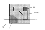
このエピタキシャルウェーハのGaAs基板側に図3(平面図)、図4(断面図)に示すようにn電極14、p型GaP層側にp電極15を具備した吸収基板型の廉価タイプ発光ダイオード13を作製することができる。吸収基板型とは、発光層から放射された光をGaAs基板が吸収してしまうため、このように言われている。
また図5(平面図)、図6(断面図)に示すように発光した光に対して透明な基板をp型GaP層側に接合し、不透明なGaAs基板を除去した後にn電極、p電極を具備して作製した所謂透明基板型とすることができる。
さらには発光した光を反射する基板をp型GaP層側に接合し、GaAs基板を除去した後にn電極、p電極を具備して作製した反射基板型の高輝度タイプ発光ダイオード16とすることができる。
基板としてはGaAs、 Si、Ge 等を用いることができるが、(100)面から<011>または<01−1>方向へ10〜20°傾斜したGaAs基板を用いることが好ましい。
As shown in FIG. 3 (plan view) and FIG. 4 (sectional view) on the GaAs substrate side of this epitaxial wafer, an absorption substrate type inexpensive type
Further, as shown in FIG. 5 (plan view) and FIG. 6 (sectional view), a substrate transparent to the emitted light is bonded to the p-type GaP layer side, and after removing the opaque GaAs substrate, an n electrode and a p electrode Thus, a so-called transparent substrate mold can be obtained.
Further, a substrate for reflecting the emitted light is bonded to the p-type GaP layer side, and after removing the GaAs substrate, a reflection substrate type high-intensity type
As the substrate, GaAs, Si, Ge, or the like can be used. However, it is preferable to use a GaAs substrate inclined by 10 to 20 ° from the (100) plane in the <011> or <01-1> direction.
次に本発明の実施例について説明する。
(実施例1)
実施例1として、図3、4に示した構造の570nm付近の波長を発光する吸収基板型発光ダイオード13を作製した。この発光素子は図1に示すように、Siをドープしたn型の(100)面から15°傾けた面を有するGaAs単結晶からなる半導体基板100上にMOCVD法により以下の層を順次成膜して作製した。n型のGaAsバッファ層111(厚さ500nm、Siドープ1×1018cm-3)、n型のAl0.5In0.5Pクラッド層112(厚さ500nm、Siドープ2×1018cm-3)、(Al0.3Ga0.7)0.5In0.5P井戸層121(厚さ4nm、アンドープ)、(Al0.7Ga0.3)0.5In0.5P障壁層122(厚さ5nm、アンドープ)、(Al0.7Ga0.3)0.5In0.5P中間層113(厚さ500nm、アンドープ)、p型のAl0.5In0.5Pクラッド層114(厚さ700nm、Mgドープ1×1018cm-3)、p型のGaP電流拡散層115(厚さ10μm、Mgドープ5×1018cm-3)の層を順次成長したエピタキシャルウェーハ11を作製した。尚、GaP層のみ740℃で成長し、他の層は670℃の温度で成膜を行った。井戸層121の層数を150とし、障壁層122の層数を149とした。
Next, examples of the present invention will be described.
(Example 1)
As Example 1, an absorption substrate type
このエピタキシャルウェーハのGaAs基板側にn電極14、p型GaP層側にp電極15を形成し、ダイシングにより300μm角の発光ダイオード10を作製した。作製した発光ダイオードをTO−18ステムにマウントし、ワイヤボンディングを行い発光ダイオードの特性を評価した。
このようにして作製した発光ダイオードの輝度は29mcdであり、井戸層数50の従来構造と比較して、2.2倍になった。
An n-
The brightness of the light-emitting diode thus fabricated was 29 mcd, which was 2.2 times that of the conventional structure having 50 well layers.
(実施例2)
実施例2として量子井戸構造における障壁層のAl比率以外は実施例1と同一条件でエピタキシャルウェーハを作製し、電極を形成した後特性を評価した。このようにして作製した発光ダイオードの輝度および輝度残存率と障壁層Al組成との関係を表1および図7、図8に示す。ここで、輝度残存率とは、ウェーハ面内からサンプリングした5個の発光ダイオードの通電後の平均輝度を、通電前の平均輝度で割ったものとした。
輝度はAl組成を大きくした方が増加するが、輝度残存率はAl組成=0.7付近が極大となった。
(Example 2)
As Example 2, an epitaxial wafer was produced under the same conditions as in Example 1 except for the Al ratio of the barrier layer in the quantum well structure, and the characteristics were evaluated after the electrodes were formed. Table 1 and FIG. 7 and FIG. 8 show the relationship between the luminance and luminance residual ratio of the light-emitting diode thus manufactured and the barrier layer Al composition. Here, the luminance remaining rate was obtained by dividing the average luminance after energization of five light emitting diodes sampled from the wafer surface by the average luminance before energization.
The luminance increases as the Al composition is increased, but the luminance residual ratio is maximized near Al composition = 0.7.

(実施例3)
実施例3として量子井戸構造における井戸層数以外は実施例1と同一条件でエピタキシャルウェーハを作製し、電極を形成した後特性を評価した。
このようにして作製した発光ダイオードの輝度と井戸層数および輝度残存率と井戸層数の関係を表2および図9、図10に示す。輝度、輝度残存率ともに層数を増やした方が良好な結果が得られるが、150層程度でほぼ横ばいになる。
(Example 3)
As Example 3, an epitaxial wafer was produced under the same conditions as Example 1 except for the number of well layers in the quantum well structure, and the characteristics were evaluated after the electrodes were formed.
Table 2 and FIG. 9 and FIG. 10 show the relationship between the luminance, the number of well layers, the luminance remaining rate, and the number of well layers of the light-emitting diode fabricated as described above. A better result can be obtained by increasing the number of layers for both luminance and luminance residual ratio, but the level is almost flat at about 150 layers.
(実施例4)
実施例4として、図5、6に示した構造の570nm付近の波長を発光する透明基板型発光ダイオード16を作製した。この発光ダイオードは実施例1同様に、Siをドープしたn型の(100)面から15°傾けた面を有するGaAs単結晶からなる半導体基板100上にMOCVD法により以下の層を順次成膜して作製した。n型のGaAsバッファ層111(厚さ500nm、Siドープ1×1018cm-3)、n型のAl0.5In0.5Pクラッド層112(厚さ500nm、Siドープ2×1018cm-3)、(Al0.2Ga0.8)0.5In0.5P井戸層121(厚さ4nm、アンドープ)、(Al0.7Ga0.3)0.5In0.5P障壁層122(厚さ5nm、アンドープ)、(Al0.7Ga0.3)0.5In0.5P中間層113(厚さ500nm、アンドープ)、p型のAl0.5In0.5Pクラッド層114(厚さ700nm、Mgドープ1×1018cm-3)、p型のGaP電流拡散層115(厚さ10μm、Mgドープ6×1018cm-3)の層を順次成長したエピタキシャルウェーハ11を作製した。尚、GaP層のみ740℃で成長し、他の層は670℃の温度で成膜を行った。井戸層121の層数を150とし、障壁層122の層数を149とした。
Example 4
As Example 4, a transparent substrate type
作製したエピタキシャルウェーハ表面に活性化接合法によりGaPを接合させて、半導体層を機械的に支持できる状態とした後、GaAs基板をウェットエッチングにより除去した。これにより発光素子の外部への取り出し効率を向上することができ、高輝度の化合物半導体LEDを構成できる。
基板を除去した面にn型の電極14を形成し、エッチングにより所定のエピ層を除去した後にp型の電極15を形成した。その後ダイシングにより300μm角の発光ダイオードを作製した。作製した発光ダイオードをTO−18ステムにマウントし、ワイヤボンディングを行い発光ダイオードの特性を評価した。
このようにして作製した発光ダイオードの輝度は105mcdであり、従来構造と比較して2.0倍になった。
GaP was bonded to the surface of the manufactured epitaxial wafer by an activation bonding method so that the semiconductor layer could be mechanically supported, and then the GaAs substrate was removed by wet etching. Thereby, the extraction efficiency to the exterior of a light emitting element can be improved, and high-intensity compound semiconductor LED can be comprised.
An n-
The luminance of the light-emitting diode thus manufactured was 105 mcd, which was 2.0 times that of the conventional structure.
本発明の発光ダイオードは赤色から黄緑色まで広い波長領域で高輝度に発光可能であり、しかも長時間の駆動における劣化が少ないので、各種のランプや青色等の発光ダイオードと組み合わせて白色ダイオードとしても利用できる。 The light-emitting diode of the present invention can emit light with high brightness in a wide wavelength range from red to yellow-green, and also has little deterioration in long-time driving. Therefore, it can be combined with various lamps and light-emitting diodes such as blue as a white diode. Available.
100 n型GaAs基板
11 エピタキシャルウェーハ
110 エピタキシャル層
111 n型バッファ層
112 n型クラッド層
113 中間層
114 p型クラッド層
115 p型GaP層
120 量子井戸構造
121 井戸層
122 障壁層
13 吸収基板型発光ダイオード
14 n型オーミック電極
15 p型オーミック電極
16 透明基板型発光ダイオード
17 透明基板
100 n-
15 p-
Claims (12)
Priority Applications (4)
| Application Number | Priority Date | Filing Date | Title |
|---|---|---|---|
| JP2007025054A JP2008192790A (en) | 2007-02-05 | 2007-02-05 | Light emitting diode |
| US12/525,789 US8164106B2 (en) | 2007-02-05 | 2008-02-04 | AIGaInP light emitting diode |
| TW097104337A TWI383518B (en) | 2007-02-05 | 2008-02-04 | Light emitting diode |
| PCT/JP2008/051751 WO2008099699A1 (en) | 2007-02-05 | 2008-02-04 | Light-emitting diode |
Applications Claiming Priority (1)
| Application Number | Priority Date | Filing Date | Title |
|---|---|---|---|
| JP2007025054A JP2008192790A (en) | 2007-02-05 | 2007-02-05 | Light emitting diode |
Publications (1)
| Publication Number | Publication Date |
|---|---|
| JP2008192790A true JP2008192790A (en) | 2008-08-21 |
Family
ID=39689943
Family Applications (1)
| Application Number | Title | Priority Date | Filing Date |
|---|---|---|---|
| JP2007025054A Pending JP2008192790A (en) | 2007-02-05 | 2007-02-05 | Light emitting diode |
Country Status (4)
| Country | Link |
|---|---|
| US (1) | US8164106B2 (en) |
| JP (1) | JP2008192790A (en) |
| TW (1) | TWI383518B (en) |
| WO (1) | WO2008099699A1 (en) |
Cited By (5)
| Publication number | Priority date | Publication date | Assignee | Title |
|---|---|---|---|---|
| US20110316020A1 (en) * | 2009-03-10 | 2011-12-29 | Showa Denko K.K. | Epitaxial wafer for light emitting diode |
| WO2012073993A1 (en) * | 2010-12-02 | 2012-06-07 | 昭和電工株式会社 | Light-emitting diode, light-emitting diode lamp, and illumination device |
| KR101422364B1 (en) * | 2009-08-07 | 2014-07-22 | 쇼와 덴코 가부시키가이샤 | Multicolour light emitting diode lamp for use in plant cultivation, lighting device and plant cultivation method |
| JP2015167245A (en) * | 2015-04-30 | 2015-09-24 | 昭和電工株式会社 | Light-emitting diode, light-emitting diode lamp and luminaire |
| US9627578B2 (en) | 2010-07-06 | 2017-04-18 | Showa Denko K.K. | Epitaxial wafer for light-emitting diodes |
Families Citing this family (3)
| Publication number | Priority date | Publication date | Assignee | Title |
|---|---|---|---|---|
| JP2010239098A (en) * | 2009-03-10 | 2010-10-21 | Showa Denko Kk | Light emitting diode, light emitting diode lamp, and lighting device |
| JP5220687B2 (en) * | 2009-06-15 | 2013-06-26 | 昭和電工株式会社 | Lighting device and plant cultivation system for plant cultivation |
| JP5801542B2 (en) | 2010-07-13 | 2015-10-28 | 昭和電工株式会社 | Light emitting diode and light emitting diode lamp |
Citations (8)
| Publication number | Priority date | Publication date | Assignee | Title |
|---|---|---|---|---|
| JPH0371679A (en) * | 1989-08-11 | 1991-03-27 | Kokusai Denshin Denwa Co Ltd <Kdd> | Semiconductor light emitting element |
| JP2002237617A (en) * | 1990-08-20 | 2002-08-23 | Toshiba Corp | Semiconductor light-emitting diode |
| JP2004047973A (en) * | 2002-05-17 | 2004-02-12 | Shin Etsu Handotai Co Ltd | Method for manufacturing light-emitting element |
| JP2005159297A (en) * | 2003-10-30 | 2005-06-16 | Sharp Corp | Semiconductor light emitting element, method for manufacturing the same, and semiconductor device |
| JP2006253180A (en) * | 2005-03-08 | 2006-09-21 | Sony Corp | Semiconductor light emitting element |
| JP2007019124A (en) * | 2005-07-06 | 2007-01-25 | Showa Denko Kk | Compound semiconductor light emitting diode and method for manufacturing the same |
| JP2007019262A (en) * | 2005-07-07 | 2007-01-25 | Toshiba Discrete Technology Kk | Semiconductor light-emitting device and manufacturing method thereof |
| JP2008084974A (en) * | 2006-09-26 | 2008-04-10 | Stanley Electric Co Ltd | Semiconductor light emitting device |
Family Cites Families (5)
| Publication number | Priority date | Publication date | Assignee | Title |
|---|---|---|---|---|
| US5153889A (en) * | 1989-05-31 | 1992-10-06 | Kabushiki Kaisha Toshiba | Semiconductor light emitting device |
| JP3373561B2 (en) * | 1992-09-30 | 2003-02-04 | 株式会社東芝 | Light emitting diode |
| JP3732626B2 (en) | 1997-08-26 | 2006-01-05 | 株式会社東芝 | Semiconductor light emitting device |
| JP3698402B2 (en) * | 1998-11-30 | 2005-09-21 | シャープ株式会社 | Light emitting diode |
| US6777257B2 (en) * | 2002-05-17 | 2004-08-17 | Shin-Etsu Handotai Co., Ltd. | Method of fabricating a light emitting device and light emitting device |
-
2007
- 2007-02-05 JP JP2007025054A patent/JP2008192790A/en active Pending
-
2008
- 2008-02-04 TW TW097104337A patent/TWI383518B/en not_active IP Right Cessation
- 2008-02-04 WO PCT/JP2008/051751 patent/WO2008099699A1/en active Application Filing
- 2008-02-04 US US12/525,789 patent/US8164106B2/en not_active Expired - Fee Related
Patent Citations (8)
| Publication number | Priority date | Publication date | Assignee | Title |
|---|---|---|---|---|
| JPH0371679A (en) * | 1989-08-11 | 1991-03-27 | Kokusai Denshin Denwa Co Ltd <Kdd> | Semiconductor light emitting element |
| JP2002237617A (en) * | 1990-08-20 | 2002-08-23 | Toshiba Corp | Semiconductor light-emitting diode |
| JP2004047973A (en) * | 2002-05-17 | 2004-02-12 | Shin Etsu Handotai Co Ltd | Method for manufacturing light-emitting element |
| JP2005159297A (en) * | 2003-10-30 | 2005-06-16 | Sharp Corp | Semiconductor light emitting element, method for manufacturing the same, and semiconductor device |
| JP2006253180A (en) * | 2005-03-08 | 2006-09-21 | Sony Corp | Semiconductor light emitting element |
| JP2007019124A (en) * | 2005-07-06 | 2007-01-25 | Showa Denko Kk | Compound semiconductor light emitting diode and method for manufacturing the same |
| JP2007019262A (en) * | 2005-07-07 | 2007-01-25 | Toshiba Discrete Technology Kk | Semiconductor light-emitting device and manufacturing method thereof |
| JP2008084974A (en) * | 2006-09-26 | 2008-04-10 | Stanley Electric Co Ltd | Semiconductor light emitting device |
Cited By (8)
| Publication number | Priority date | Publication date | Assignee | Title |
|---|---|---|---|---|
| US20110316020A1 (en) * | 2009-03-10 | 2011-12-29 | Showa Denko K.K. | Epitaxial wafer for light emitting diode |
| US8482027B2 (en) * | 2009-03-10 | 2013-07-09 | Showa Denko K.K. | Epitaxial wafer for light emitting diode |
| KR101422364B1 (en) * | 2009-08-07 | 2014-07-22 | 쇼와 덴코 가부시키가이샤 | Multicolour light emitting diode lamp for use in plant cultivation, lighting device and plant cultivation method |
| US9627578B2 (en) | 2010-07-06 | 2017-04-18 | Showa Denko K.K. | Epitaxial wafer for light-emitting diodes |
| WO2012073993A1 (en) * | 2010-12-02 | 2012-06-07 | 昭和電工株式会社 | Light-emitting diode, light-emitting diode lamp, and illumination device |
| JP2012119585A (en) * | 2010-12-02 | 2012-06-21 | Showa Denko Kk | Light-emitting diode, light-emitting diode lamp and luminaire |
| US9299885B2 (en) | 2010-12-02 | 2016-03-29 | Showa Denko K.K. | Light-emitting diode, light-emitting diode lamp, and illumination device |
| JP2015167245A (en) * | 2015-04-30 | 2015-09-24 | 昭和電工株式会社 | Light-emitting diode, light-emitting diode lamp and luminaire |
Also Published As
| Publication number | Publication date |
|---|---|
| US8164106B2 (en) | 2012-04-24 |
| TW200849667A (en) | 2008-12-16 |
| WO2008099699A1 (en) | 2008-08-21 |
| TWI383518B (en) | 2013-01-21 |
| US20100006818A1 (en) | 2010-01-14 |
Similar Documents
| Publication | Publication Date | Title |
|---|---|---|
| US7291865B2 (en) | Light-emitting semiconductor device | |
| JP3698402B2 (en) | Light emitting diode | |
| CN100448041C (en) | Semiconductor light emitting element | |
| JP4954536B2 (en) | Nitride semiconductor light emitting device | |
| KR101611412B1 (en) | Light emitting device | |
| US20070075319A1 (en) | Semiconductor light-emitting device with transparent conductive film | |
| US20110037049A1 (en) | Nitride semiconductor light-emitting device | |
| JP2008192790A (en) | Light emitting diode | |
| JPH0823124A (en) | Light-emitting element of gallium nitride compound semiconductor | |
| JP2010263085A (en) | Light emitting element | |
| KR101262854B1 (en) | Nitride light emitting device | |
| JP2010067903A (en) | Light emitting element | |
| JP2007096166A (en) | Semiconductor light emitting device | |
| JP2010056423A (en) | Electrode for semiconductor light-emitting element, and semiconductor light emitting element | |
| JP2002344015A (en) | Nitride semiconductor light-emitting element | |
| JP2007109885A (en) | Semiconductor light emitting device and manufacturing method thereof | |
| JP2006040998A (en) | Semiconductor light emitting device, epitaxial wafer for semiconductor light emitting device | |
| WO2012117795A1 (en) | Light-emitting diode | |
| JP5162809B2 (en) | Nitride semiconductor device | |
| JP2006310488A (en) | Group iii nitride-based semiconductor light emitting device and its manufacturing method | |
| KR102399381B1 (en) | Light emitting device | |
| JP2004342732A (en) | Oxide semiconductor light emitting device | |
| JP2006261219A (en) | Semiconductor light emitting device | |
| KR102340717B1 (en) | Light Emitting Device and Method for the same | |
| JP2007096168A (en) | Semiconductor light emitting device |
Legal Events
| Date | Code | Title | Description |
|---|---|---|---|
| A621 | Written request for application examination |
Free format text: JAPANESE INTERMEDIATE CODE: A621 Effective date: 20091106 |
|
| A131 | Notification of reasons for refusal |
Free format text: JAPANESE INTERMEDIATE CODE: A131 Effective date: 20120612 |
|
| A02 | Decision of refusal |
Free format text: JAPANESE INTERMEDIATE CODE: A02 Effective date: 20121016 |