JP2008172040A - Semiconductor light emitting device, method for manufacturing semiconductor light emitting device, backlight, display, and electronic device - Google Patents
Semiconductor light emitting device, method for manufacturing semiconductor light emitting device, backlight, display, and electronic device Download PDFInfo
- Publication number
- JP2008172040A JP2008172040A JP2007003989A JP2007003989A JP2008172040A JP 2008172040 A JP2008172040 A JP 2008172040A JP 2007003989 A JP2007003989 A JP 2007003989A JP 2007003989 A JP2007003989 A JP 2007003989A JP 2008172040 A JP2008172040 A JP 2008172040A
- Authority
- JP
- Japan
- Prior art keywords
- light emitting
- layer
- semiconductor
- semiconductor layer
- metal electrode
- Prior art date
- Legal status (The legal status is an assumption and is not a legal conclusion. Google has not performed a legal analysis and makes no representation as to the accuracy of the status listed.)
- Pending
Links
Images


Landscapes
- Led Devices (AREA)
- Led Device Packages (AREA)
Abstract
【課題】電極のコンタクト抵抗の低減により動作電圧の低減を図ることができるとともに、光取り出し効率の向上により発光効率の大幅な向上を図ることができ、しかも製造が容易な半導体発光素子およびその製造方法を提供する。
【解決手段】第1の導電型の第1の半導体層11、12と第2の導電型の第2の半導体層14との間に発光層13を挟んだ構造を有し、第1の半導体層11に金属電極17がコンタクトしている半導体発光素子において、金属電極17を第1の半導体層12に埋め込むようにする。金属電極17の第1の半導体層11に埋め込まれていない方の面と第1の半導体層11の主面とをほぼ同一平面とする。
【選択図】図1A semiconductor light emitting device capable of reducing operating voltage by reducing contact resistance of an electrode and greatly improving light emitting efficiency by improving light extraction efficiency, and manufacturing thereof easily Provide a method.
A light emitting layer 13 is sandwiched between first semiconductor layers 11 and 12 of a first conductivity type and a second semiconductor layer 14 of a second conductivity type, and the first semiconductor In the semiconductor light emitting device in which the metal electrode 17 is in contact with the layer 11, the metal electrode 17 is embedded in the first semiconductor layer 12. The surface of the metal electrode 17 that is not embedded in the first semiconductor layer 11 and the main surface of the first semiconductor layer 11 are substantially coplanar.
[Selection] Figure 1
Description
この発明は、半導体発光素子、半導体発光素子の製造方法、バックライト、ディスプレイおよび電子機器に関し、例えば、窒化物系III−V族化合物半導体を用いた発光ダイオードおよびこの発光ダイオードを用いた各種の装置または機器に適用して好適なものである。 The present invention relates to a semiconductor light emitting device, a method for manufacturing a semiconductor light emitting device, a backlight, a display, and an electronic device. For example, a light emitting diode using a nitride III-V compound semiconductor and various devices using the light emitting diode Or it is a thing suitable for applying to an apparatus.
GaN系発光ダイオードは、通常、サファイア基板上に発光ダイオード構造を形成するGaN系半導体層、具体的には、n型GaN層、InGaN系の発光層(活性層)、p型GaN層などを順次成長させることにより製造される。この場合、p側電極はp型GaN層上に形成することができるが、n側電極は、サファイア基板に導電性がないため基板裏面側に形成することができない。このため、従来は、発光ダイオード構造を形成するGaN系半導体層の成長後に、p型GaN層、活性層およびn型GaN層の上層部を所定のメサ形状にパターニングし、このメサ部のp型GaN層上にp側電極を、このメサ部に隣接する部分のn型GaN層上にn側電極を形成するのが一般的であった。ところが、この発光ダイオードでは、光取り出し効率を十分に大きくすることが困難である。そこで、近年では、発光ダイオードの光取り出し効率の向上を図る見地から、発光ダイオード構造を形成するGaN系半導体層の成長後に、レーザ剥離法などによりサファイア基板を剥離し、n型GaN層の裏面を露出させ、その面にリソグラフィー技術および真空蒸着などの成膜技術を用いてn側電極を形成することが多くなっている。 A GaN-based light emitting diode is usually a GaN-based semiconductor layer that forms a light-emitting diode structure on a sapphire substrate, specifically an n-type GaN layer, an InGaN-based light-emitting layer (active layer), a p-type GaN layer, etc. Manufactured by growing. In this case, the p-side electrode can be formed on the p-type GaN layer, but the n-side electrode cannot be formed on the back side of the substrate because the sapphire substrate has no conductivity. For this reason, conventionally, after the growth of the GaN-based semiconductor layer forming the light emitting diode structure, the p-type GaN layer, the active layer, and the upper layer of the n-type GaN layer are patterned into a predetermined mesa shape. In general, a p-side electrode is formed on the GaN layer, and an n-side electrode is formed on the n-type GaN layer adjacent to the mesa portion. However, in this light emitting diode, it is difficult to sufficiently increase the light extraction efficiency. Therefore, in recent years, from the viewpoint of improving the light extraction efficiency of the light emitting diode, after the growth of the GaN-based semiconductor layer forming the light emitting diode structure, the sapphire substrate is peeled off by a laser peeling method or the like, and the back surface of the n-type GaN layer is In many cases, the n-side electrode is formed on the exposed surface by using a lithography technique and a film forming technique such as vacuum deposition.
なお、基板上に成長マスクを形成し、この成長マスクを用いて基板上に窒化物系III−V族化合物半導体を選択成長させるようにした窒化物系III−V族化合物半導体の成長方法において、成長マスクとして少なくとも最表面が窒化物(窒化シリコンまたは窒化チタン)からなる多層膜を用いることが提案されている(特許文献1参照。)が、特許文献1には、金属電極を半導体層に埋め込むことについては何ら開示されていない。
しかしながら、発光ダイオード構造を形成するGaN系半導体層の成長後にサファイア基板を剥離した後、n型GaN層の裏面にn側電極を形成する上述の従来の方法では、n側電極の高さがかなり大きくなってしまい、n側電極の高さを低くするためにn型GaN層を反応性イオンエッチング(RIE)法などにより裏面側から部分的にエッチングして凹部を形成し、この凹部にn側電極を形成するとn側電極のコンタクト抵抗が増加し、良好なコンタクトが取りにくくなる。 However, in the above-described conventional method in which the n-side electrode is formed on the back surface of the n-type GaN layer after the sapphire substrate is peeled off after the growth of the GaN-based semiconductor layer forming the light emitting diode structure, the height of the n-side electrode is considerably high. In order to reduce the height of the n-side electrode, the n-type GaN layer is partially etched from the back side by a reactive ion etching (RIE) method or the like to form a recess. When the electrode is formed, the contact resistance of the n-side electrode increases, making it difficult to obtain a good contact.
そこで、この発明が解決しようとする課題は、電極のコンタクト抵抗の低減により動作電圧の低減を図ることができるとともに、光取り出し効率の向上により発光効率の大幅な向上を図ることができ、しかも製造が容易な半導体発光素子およびその製造方法を提供することである。
この発明が解決しようとする他の課題は、上記のような優れた半導体発光素子を用いたバックライト、ディスプレイおよび電子機器を提供することである。
上記課題および他の課題は、添付図面を参照した本明細書の記述により明らかとなるであろう。
Therefore, the problem to be solved by the present invention is that the operating voltage can be reduced by reducing the contact resistance of the electrode, and the luminous efficiency can be greatly improved by improving the light extraction efficiency. It is an object of the present invention to provide a semiconductor light emitting device and a method for manufacturing the same.
Another problem to be solved by the present invention is to provide a backlight, a display, and an electronic apparatus using the excellent semiconductor light emitting element as described above.
The above and other problems will become apparent from the description of this specification with reference to the accompanying drawings.
上記課題を解決するために、第1の発明は、
第1の導電型の第1の半導体層と第2の導電型の第2の半導体層との間に発光層を挟んだ構造を有し、上記第1の半導体層に金属電極がコンタクトしている半導体発光素子において、
上記金属電極が上記第1の半導体層に埋め込まれている
ことを特徴とするものである。
In order to solve the above problem, the first invention is:
A light emitting layer is sandwiched between a first semiconductor layer of a first conductivity type and a second semiconductor layer of a second conductivity type, and a metal electrode contacts the first semiconductor layer. In the semiconductor light emitting device
The metal electrode is embedded in the first semiconductor layer.
発光素子構造を形成する半導体層には、必要に応じて、第1の半導体層、発光層および第2の半導体層以外のものが含まれてもよい。金属電極は第1の半導体層の成長に先立って形成され、この金属電極を覆うように第1の半導体層を成長させることによりこの金属電極が第1の半導体層に埋め込まれる。この金属電極の埋め込みは、一般的にはこの第1の半導体層の横方向成長を利用して行われる。この金属電極の一方向の幅は、この金属電極の埋め込みが良好に行われ、結晶性の良好な半導体層が得られるようにする観点から、好ましくは2μm以下とし、コンタクト抵抗が高くなり過ぎないようにする観点から、例えば1〜2μm程度とする。好ましくは、金属電極の第1の半導体層に埋め込まれていない方の面とこの第1の半導体層の主面とがほぼ同一平面上にあるようにするが、これに限定されるものではない。必要に応じて、金属電極の第1の半導体層に埋め込まれている方の面と第1の半導体層との間に、発光層から発生した光を反射する誘電体膜を設けてもよい。 The semiconductor layer forming the light-emitting element structure may include a layer other than the first semiconductor layer, the light-emitting layer, and the second semiconductor layer as necessary. The metal electrode is formed prior to the growth of the first semiconductor layer. The metal electrode is embedded in the first semiconductor layer by growing the first semiconductor layer so as to cover the metal electrode. The embedding of the metal electrode is generally performed by utilizing the lateral growth of the first semiconductor layer. The width in one direction of the metal electrode is preferably 2 μm or less from the viewpoint of satisfactorily embedding the metal electrode and obtaining a semiconductor layer with good crystallinity, and the contact resistance does not become too high. From the viewpoint of doing so, for example, it is about 1 to 2 μm. Preferably, the surface of the metal electrode not embedded in the first semiconductor layer and the main surface of the first semiconductor layer are substantially coplanar, but the present invention is not limited to this. . If necessary, a dielectric film that reflects light generated from the light emitting layer may be provided between the surface of the metal electrode embedded in the first semiconductor layer and the first semiconductor layer.
金属電極の第1の半導体層に埋め込まれている方の面を、この金属電極を有する側の第1の半導体層の主面に対して傾斜させるか、この金属電極の第1の半導体層に埋め込まれている方の面を、この金属電極の第1の半導体層に埋め込まれていない方の面に対して傾斜させてもよい。この場合、上記の主面は、典型的には光取り出し面である。
光取り出し効率の向上や実装の容易さの観点より、発光素子構造を形成する半導体層は光取り出し面およびその反対側の面にそれぞれ第1の電極としての金属電極および第2の電極を有するものの方が好ましいが、これに限定されるものではなく、片面に第1の電極および第2の電極を有するものであってもよい。
The surface of the metal electrode embedded in the first semiconductor layer is inclined with respect to the main surface of the first semiconductor layer on the side having the metal electrode, or the first surface of the metal electrode is covered with the first semiconductor layer. The embedded surface may be inclined with respect to the surface of the metal electrode not embedded in the first semiconductor layer. In this case, the main surface is typically a light extraction surface.
From the viewpoint of improving light extraction efficiency and ease of mounting, the semiconductor layer forming the light emitting element structure has a metal electrode as a first electrode and a second electrode on the light extraction surface and the opposite surface, respectively. However, the present invention is not limited to this, and the first electrode and the second electrode may be provided on one side.
光取り出し面に金属電極を有する場合、この金属電極は、この金属電極が埋め込み電極であるため、発光層からの光はこの金属電極に当たって方向が変わりやすく、さらに、後述のように、この金属電極自体を高反射電極としたり、いわゆるODR電極としたり、金属電極の埋め込まれている側の面を傾斜させるなどして、この金属電極を光取り出し効率の向上に適した構造とすることができるので、この金属電極は必ずしも面積を小さくすることなく形成することが可能である。
金属電極は、任意の平面形状であってよいが、典型的には、円弧状、長方形、円形、多角形、リング形状などの幾何学模様の平面形状を有するものが用いられるほか、これらの幾何学模様の所定の繰り返しパターン、具体的には、メッシュ状のものや、複数のドットを等間隔にグリッド状に配置したものを用いてもよい。
When a metal electrode is provided on the light extraction surface, this metal electrode is a buried electrode, so that the light from the light emitting layer is easily changed in direction upon hitting the metal electrode. Since the metal electrode itself can be a highly reflective electrode, a so-called ODR electrode, or the surface on which the metal electrode is embedded can be inclined to make the metal electrode suitable for improving light extraction efficiency. This metal electrode can be formed without necessarily reducing the area.
The metal electrode may have an arbitrary planar shape, but typically, a metal electrode having a geometrical planar shape such as an arc shape, a rectangular shape, a circular shape, a polygonal shape, a ring shape, or the like is used. A predetermined repetitive pattern of a geometric pattern, specifically, a mesh shape or a plurality of dots arranged in a grid at equal intervals may be used.
金属電極の材料としては、第1の半導体層と良好なコンタクトを取ることができ、かつ光取り出し効率の向上の観点から、好ましくは、発光層からの光に対する反射率の高いものが用いられる。ここで、発光層からの光に対して反射率の高い材料を用いるのは次のような理由による。すなわち、金属電極が発光素子構造を形成する半導体層の光取り出し面に設けられる場合、この金属電極によって光取り出し面が遮光されるが、この金属電極を高反射電極に構成すると、この金属電極に光が当たることによって反射され、さらに半導体発光素子の内部で反射されることにって光取り出し面から外部に効率的に取り出すことができる。この場合、半導体発光素子にさらに反射部を設けることによって、所望の光を取り出すことが可能である。このような金属電極の材料としては、具体的には例えばRhが最も好ましい。Rhは融点が1963℃と極めて高く、窒化物系III−V族化合物半導体を成長させる際の1000℃程度の高い温度でも融解することがなく、しかも可視光に対する反射率が77〜80%と高い。ただし、Rh以外の金属、例えばNi、W、Tiなどを用いてもよい。これらの金属はいずれも高融点金属であり、窒化物系III−V族化合物半導体を成長させる際の温度でも融解しない。また、この金属電極は、上記した金属の多層膜からなるものであってもよい。 As a material for the metal electrode, a material having a high reflectivity with respect to light from the light emitting layer is preferably used from the viewpoint of making good contact with the first semiconductor layer and improving light extraction efficiency. Here, the reason why a material having a high reflectance with respect to light from the light emitting layer is used is as follows. That is, when the metal electrode is provided on the light extraction surface of the semiconductor layer forming the light emitting element structure, the light extraction surface is shielded by the metal electrode. The light is reflected when it hits, and further reflected inside the semiconductor light emitting element, so that it can be efficiently taken out from the light extraction surface. In this case, it is possible to extract desired light by further providing a reflective portion in the semiconductor light emitting element. Specifically, for example, Rh is most preferable as a material for such a metal electrode. Rh has an extremely high melting point of 1963 ° C., does not melt even at a high temperature of about 1000 ° C. when growing a nitride III-V compound semiconductor, and has a high reflectance of 77 to 80% for visible light. . However, metals other than Rh, such as Ni, W, Ti, etc. may be used. These metals are all refractory metals and do not melt even at the temperature at which the nitride III-V compound semiconductor is grown. Further, the metal electrode may be composed of a multilayer film of the metal described above.
発光素子構造を形成する半導体層、具体的には、第1の半導体層、活性層および第2の半導体層ならびに後述の第3の半導体層の材料としては、種々の半導体を用いることができるが、例えば、窒化物系III−V族化合物半導体が挙げられる。窒化物系III−V族化合物半導体は、III族元素としてAl、B、Ga、InおよびTlからなる群より選ばれた少なくとも一種の元素を含み、一般的には、AlX By Ga1-x-y-z Inz Asu N1-u-v Pv (ただし、0≦x≦1、0≦y≦1、0≦z≦1、0≦u≦1、0≦v≦1、0≦x+y+z<1、0≦u+v<1)からなり、より具体的には、AlX By Ga1-x-y-z Inz N(ただし、0≦x≦1、0≦y≦1、0≦z≦1、0≦x+y+z<1)からなり、典型的にはAlX Ga1-x-z Inz N(ただし、0≦x≦1、0≦z≦1)からなる。窒化物系III−V族化合物半導体の具体例を挙げると、GaN、InN、AlN、AlGaN、InGaN、AlGaInNなどである。これら以外に、Tlx Iny Alz Ga1-x-y-z N(ただし、0<x≦1、0≦y<1、0≦z<1、0<x+y+z<1)を用いてもよい。第1の導電型は典型的にはn型であるがp型であってもよく、それに応じて第2の導電型はp型またはn型である。
第1の半導体層、活性層および第2の半導体層が窒化物系III−V族化合物半導体からなる場合、金属電極は、良好なオーミックコンタクト特性を得る観点より、第1の半導体層のC+面よりもC−面にコンタクトしていることが望ましい。これは、金属電極を覆うように第1の半導体層を成長させる際に、この第1の半導体層のC−面が金属電極とコンタクトする方がその成長温度でこの第1の半導体層と金属電極との界面で合金化が起きやすいためである。
Various semiconductors can be used as materials for the semiconductor layer forming the light-emitting element structure, specifically, the first semiconductor layer, the active layer, the second semiconductor layer, and the third semiconductor layer described later. Examples thereof include nitride III-V compound semiconductors. Nitride III-V compound semiconductor comprises Al, B, Ga, at least one selected from the group consisting of In and Tl as group III elements, in general, Al X B y Ga 1- xyz In z As u N 1- uv P v ( However, 0 ≦ x ≦ 1,0 ≦ y ≦ 1,0 ≦ z ≦ 1,0 ≦ u ≦ 1,0 ≦ v ≦ 1,0 ≦ x + y + z <1, 0 ≦ u + v consists <1), more specifically, Al X B y Ga 1- xyz in z N ( However, 0 ≦ x ≦ 1,0 ≦ y ≦ 1,0 ≦ z ≦ 1,0 ≦ x + y + z <1), typically Al x Ga 1 -xz In z N (where 0 ≦ x ≦ 1, 0 ≦ z ≦ 1). Specific examples of the nitride III-V compound semiconductor include GaN, InN, AlN, AlGaN, InGaN, and AlGaInN. In addition to these, Tl x In y Al z Ga 1-xyz N (where 0 <x ≦ 1, 0 ≦ y <1, 0 ≦ z <1, 0 <x + y + z <1) may be used. The first conductivity type is typically n-type, but may be p-type, and the second conductivity type is accordingly p-type or n-type.
When the first semiconductor layer, the active layer, and the second semiconductor layer are made of a nitride-based III-V group compound semiconductor, the metal electrode has a C + surface of the first semiconductor layer from the viewpoint of obtaining good ohmic contact characteristics. It is desirable to contact the C-plane rather than. This is because when the first semiconductor layer is grown so as to cover the metal electrode, the C-plane of the first semiconductor layer is in contact with the metal electrode at the growth temperature. This is because alloying easily occurs at the interface with the electrode.
半導体発光素子の最大寸法は、必要に応じて決めることができるが、一般的には例えば1mm以下あるいは例えば300μm以下あるいは例えば100μm以下、好適には50μm以下、典型的には30μm以下、より典型的には25μm以下である。半導体発光素子は、典型的には発光ダイオードであるが、これに限定されるものではない。 The maximum dimension of the semiconductor light-emitting element can be determined as necessary, but is generally 1 mm or less, for example 300 μm or less, or for example 100 μm or less, preferably 50 μm or less, typically 30 μm or less, more typically Is 25 μm or less. The semiconductor light emitting device is typically a light emitting diode, but is not limited thereto.
発光層は、典型的には、井戸層と障壁層とが交互に積層された多重量子井戸(MQW)構造を有する。このMQW構造を有する発光層における井戸層密度はその厚さ方向に一定であってもよいが、半導体発光素子の動作電流密度の増加に伴う発光波長の大きなシフトを抑制し、しかも一層広範囲の輝度制御を行うことができるようにする観点からは、第1の半導体層がn型、第2の半導体層がp型である場合、この発光層の第1の半導体層側の井戸層密度をd1 、第2の半導体層側の井戸層密度をd2 としたとき、d1 <d2 を満足するように発光層における井戸層を配置する。このように発光層における井戸層密度を異ならせるためには、例えば、井戸層の厚さを一定とし、障壁層の厚さを異ならせる(具体的には、発光層における第2の半導体層側の障壁層の厚さを、第1の半導体層側の障壁層の厚さよりも小さくする)のが好ましいが、これに限定されるものではなく、障壁層の厚さを一定とし、井戸層の厚さを異ならせる(具体的には、発光層における第2の半導体層側の井戸層の厚さを、第1の半導体層側の井戸層の厚さよりも大きくする)ようにしてよいし、井戸層の厚さおよび障壁層の厚さの両方を異ならせてもよい。 The light emitting layer typically has a multiple quantum well (MQW) structure in which well layers and barrier layers are alternately stacked. Although the well layer density in the light emitting layer having the MQW structure may be constant in the thickness direction, it suppresses a large shift in the emission wavelength accompanying an increase in the operating current density of the semiconductor light emitting device, and further, a wider range of luminance. From the viewpoint of enabling control, when the first semiconductor layer is n-type and the second semiconductor layer is p-type, the density of the well layer on the first semiconductor layer side of the light-emitting layer is defined as d. 1 , where the well layer density on the second semiconductor layer side is d 2 , the well layers in the light emitting layer are arranged so as to satisfy d 1 <d 2 . In order to vary the well layer density in the light emitting layer in this manner, for example, the thickness of the well layer is made constant and the thickness of the barrier layer is made different (specifically, the second semiconductor layer side in the light emitting layer). The thickness of the barrier layer of the first semiconductor layer is preferably smaller than the thickness of the barrier layer on the first semiconductor layer side), but is not limited to this. The thickness may be made different (specifically, the thickness of the well layer on the second semiconductor layer side in the light emitting layer is made larger than the thickness of the well layer on the first semiconductor layer side), Both the thickness of the well layer and the thickness of the barrier layer may be different.
ここで、井戸層密度d1 および井戸層密度d2 は以下のように定義する。すなわち、総厚t0 の発光層を厚さ方向に2つに分割したとき、第1の半導体層側の発光層の領域である第1領域の厚さをt1 、第2の半導体層側の発光層の領域である第2領域の厚さをt2 とする。ただし、t0 =t1 +t2 である。また、第1領域に含まれる井戸層の数をWL1 (正数であり、整数には限定されない)、第2領域に含まれる井戸層の数をWL2 (正数であり、整数には限定されず、井戸層の総数WL=WL1 +WL2 )とする。なお、第1領域と第2領域とに跨がって1つの井戸層(厚さtIF)が存在する場合には、第1領域内のみに含まれる井戸層の数をWL’1 、第2領域内のみに含まれる井戸層の数をWL’2 とし、第1領域と第2領域とに跨がった井戸層における第1領域に含まれる厚さを厚さtIF-1、第2領域に含まれる厚さを厚さtIF-2(tIF=tIF-1+tIF-2)としたとき、
WL1 =WL’1 +ΔWL1
WL2 =WL’2 +ΔWL2
である。ただし、
ΔWL1 +ΔWL2 =1
であり、
WL=WL1 +WL2
=WL’1 +WL’2 +1
ΔWL1 =tIF-1/tIF
ΔWL2 =tIF-2/tIF
である。
Here, the well layer density d 1 and the well layer density d 2 are defined as follows. That is, when the light emitting layer having the total thickness t 0 is divided into two in the thickness direction, the thickness of the first region, which is the region of the light emitting layer on the first semiconductor layer side, is t 1 , and the second semiconductor layer side The thickness of the second region which is the region of the light emitting layer is t 2 . However, t 0 = t 1 + t 2 . In addition, the number of well layers included in the first region is WL 1 (positive number, not limited to an integer), and the number of well layers included in the second region is WL 2 (positive number, which is an integer) Without limitation, the total number of well layers is WL = WL 1 + WL 2 ). When one well layer (thickness t IF ) exists across the first region and the second region, the number of well layers included only in the first region is WL ′ 1 , WL ′ 2 is the number of well layers included only in the two regions, and the thickness included in the first region in the well layer straddling the first region and the second region is the thickness t IF-1 , When the thickness included in the two regions is the thickness t IF-2 (t IF = t IF-1 + t IF-2 )
WL 1 = WL ′ 1 + ΔWL 1
WL 2 = WL ′ 2 + ΔWL 2
It is. However,
ΔWL 1 + ΔWL 2 = 1
And
WL = WL 1 + WL 2
= WL ' 1 + WL' 2 +1
ΔWL 1 = t IF-1 / t IF
ΔWL 2 = t IF-2 / t IF
It is.
そして、井戸層密度d1 および井戸層密度d2 は以下の式から求めることができる。ただし、k≡(t0 /WL)である。
d1 =(WL1 /WL)/(t1 /t0 )
=k(WL1 /t1 ) (1)
d2 =(WL2 /WL)/(t2 /t0 )
=k(WL2 /t2 ) (2)
The well layer density d 1 and the well layer density d 2 can be obtained from the following equations. However, k≡ (t 0 / WL).
d 1 = (WL 1 / WL) / (t 1 / t 0 )
= K (WL 1 / t 1 ) (1)
d 2 = (WL 2 / WL) / (t 2 / t 0 )
= K (WL 2 / t 2 ) (2)
ここで、発光層における第1の半導体層側の界面から厚さ(2t0 /3)までの第1領域内の井戸層密度をd1 、第2の半導体層側の界面から厚さ(t0 /3)までの第2領域内の井戸層密度をd2 としたとき、d1 <d2 を満足するように発光層における井戸層が配置されている構成とすることができ、あるいは、発光層における第1の半導体層側の界面から厚さ(t0 /2)までの第1領域内の井戸層密度をd1 、第2の半導体層側の界面から厚さ(t0 /2)までの第2領域内の井戸層密度をd2 としたとき、d1 <d2 を満足するように発光層における井戸層が配置されている構成とすることができ、あるいは、発光層における第1の半導体層側の界面から厚さ(t0 /3)までの第1領域内の井戸層密度をd1 、第2の半導体層側の界面から厚さ(2t0 /3)までの第2領域内の井戸層密度をd2 としたとき、d1 <d2 を満足するように発光層における井戸層が配置されている構成とすることができる。ここで、1<d2 /d1 ≦20、好ましくは1.2≦d2 /d1 ≦10、より好ましくは1.5≦d2 /d1 ≦5を満足するように、発光層における井戸層が配置されていることが望ましい。発光層における井戸層の数(WL)は、2以上、好ましくは4以上である。 The thickness from the interface of the first semiconductor layer side of the light-emitting layer of (2t 0/3) d 1 of the well layer density of the first region to the thickness from the interface of the second semiconductor layer side (t (0/3 ) where the well layer density in the second region is d 2 , the well layer in the light emitting layer may be arranged so as to satisfy d 1 <d 2 , or the thickness from the interface of the first semiconductor layer side of the light-emitting layer (t 0/2) of the well layer density in the first area to d 1, the thickness from the interface of the second semiconductor layer side (t 0/2 ) Where the well layer density in the second region is d 2 , the well layer in the light emitting layer can be arranged so as to satisfy d 1 <d 2 , or in the light emitting layer the first semiconductor layer side of the thick from the interface (t 0/3) the well layer density in the first area to d 1, the second semiconductor layer side When the well layer density of the second region to a thickness from the surface (2t 0/3) was d 2, a structure in which well layers in the light emitting layer is arranged so as to satisfy the d 1 <d 2 be able to. In the light emitting layer, 1 <d 2 / d 1 ≦ 20, preferably 1.2 ≦ d 2 / d 1 ≦ 10, more preferably 1.5 ≦ d 2 / d 1 ≦ 5 is satisfied. It is desirable that a well layer is disposed. The number of well layers (WL) in the light emitting layer is 2 or more, preferably 4 or more.
上述のような発光層を有する半導体発光素子においては、動作電流密度を30A/cm2 としたときの発光層の発光波長をλ2 (nm)、動作電流密度を300A/cm2 としたときの発光層の発光波長をλ3 (nm)としたとき、
500(nm)≦λ2 ≦550(nm)
0≦|λ2 −λ3 |≦5(nm)
を満足することが望ましく、あるいは、動作電流密度を1A/cm2 としたときの発光層の発光波長をλ1 (nm)、動作電流密度を30A/cm2 としたときの発光層の発光波長をλ2 (nm)、動作電流密度を300A/cm2 としたときの発光層の発光波長をλ3 (nm)としたとき、
500(nm)≦λ2 ≦550(nm)
0≦|λ1 −λ2 |≦10(nm)
0≦|λ2 −λ3 |≦5(nm)
を満足することが望ましい。なお、この半導体発光素子の動作電流密度とは、動作電流値を発光層面積(接合領域の面積)で除した値である。
In the semiconductor light emitting device having the light emitting layer as described above, when the operating current density is 30 A / cm 2 , the emission wavelength of the light emitting layer is λ 2 (nm) and the operating current density is 300 A / cm 2. When the emission wavelength of the light emitting layer is λ 3 (nm),
500 (nm) ≦ λ 2 ≦ 550 (nm)
0 ≦ | λ 2 −λ 3 | ≦ 5 (nm)
It is desirable to satisfy the or an emission wavelength of the light emitting layer when the operating current density 1A / cm 2 λ 1 (nm ), emission wavelength of the light emitting layer when the operating current density was 30A / cm 2 Is λ 2 (nm), and the emission wavelength of the light emitting layer when the operating current density is 300 A / cm 2 is λ 3 (nm),
500 (nm) ≦ λ 2 ≦ 550 (nm)
0 ≦ | λ 1 −λ 2 | ≦ 10 (nm)
0 ≦ | λ 2 −λ 3 | ≦ 5 (nm)
It is desirable to satisfy The operating current density of the semiconductor light emitting element is a value obtained by dividing the operating current value by the area of the light emitting layer (area of the junction region).
あるいは、上述のような発光層を有する半導体発光素子において、動作電流密度を30A/cm2 としたときの発光層の発光波長をλ2 (nm)、動作電流密度を300A/cm2 としたときの発光層の発光波長をλ3 (nm)としたとき、
430(nm)≦λ2 ≦480(nm)
0≦|λ2 −λ3 |≦2(nm)
を満足することが望ましく、あるいは、動作電流密度を1A/cm2 としたときの発光層の発光波長をλ1 (nm)、動作電流密度を30A/cm2 としたときの発光層の発光波長をλ2 (nm)、動作電流密度を300A/cm2 としたときの発光層の発光波長をλ3 (nm)としたとき、
430(nm)≦λ2 ≦480(nm)
0≦|λ1 −λ2 |≦5(nm)
0≦|λ2 −λ3 |≦2(nm)
を満足することが望ましい。
この第1の発明による半導体発光素子は各種の装置または機器(バックライト、ディスプレイ、照明装置、電子機器など)に用いることができる。
Alternatively, in the semiconductor light emitting device having the light emitting layer as described above, when the operating current density is 30 A / cm 2 , the emission wavelength of the light emitting layer is λ 2 (nm) and the operating current density is 300 A / cm 2. When the emission wavelength of the light emitting layer is λ 3 (nm),
430 (nm) ≦ λ 2 ≦ 480 (nm)
0 ≦ | λ 2 −λ 3 | ≦ 2 (nm)
It is desirable to satisfy the or an emission wavelength of the light emitting layer when the operating current density 1A / cm 2 λ 1 (nm ), emission wavelength of the light emitting layer when the operating current density was 30A / cm 2 Is λ 2 (nm), and the emission wavelength of the light emitting layer when the operating current density is 300 A / cm 2 is λ 3 (nm),
430 (nm) ≦ λ 2 ≦ 480 (nm)
0 ≦ | λ 1 −λ 2 | ≦ 5 (nm)
0 ≦ | λ 2 −λ 3 | ≦ 2 (nm)
It is desirable to satisfy
The semiconductor light emitting device according to the first invention can be used in various devices or devices (backlight, display, illumination device, electronic device, etc.).
第2の発明は、
第1の導電型の第1の半導体層と第2の導電型の第2の半導体層との間に発光層を挟んだ構造を有し、上記第1の半導体層に金属電極がコンタクトしている半導体発光素子の製造方法において、
基板上に第1の導電型の第3の半導体層を成長させる工程と、
上記第3の半導体層上に上記金属電極を形成する工程と、
上記金属電極を覆うように上記第1の半導体層を成長させる工程と、
上記第1の半導体層上に上記発光層および上記第2の半導体層を順次成長させる工程とを有する
ことを特徴とするものである。
The second invention is
A light emitting layer is sandwiched between a first semiconductor layer of a first conductivity type and a second semiconductor layer of a second conductivity type, and a metal electrode contacts the first semiconductor layer. In the method for manufacturing a semiconductor light emitting device,
Growing a third semiconductor layer of a first conductivity type on a substrate;
Forming the metal electrode on the third semiconductor layer;
Growing the first semiconductor layer so as to cover the metal electrode;
A step of sequentially growing the light emitting layer and the second semiconductor layer on the first semiconductor layer.
典型的には、第3の半導体層から基板を剥離した後、第3の半導体層を裏面側からエッチングまたは研磨することにより金属電極を露出させる工程を有するが、これに限定されるものではない。また、例えば、第1の半導体層を成長させる際に、第1の成長温度で第1の半導体層を成長させて金属電極を覆った後、第1の成長温度よりも高い第2の成長温度で第1の半導体層を成長させるようにしてもよい。第3の半導体層上に誘電体膜および金属電極を順次形成し、その上に第1の半導体層を成長させるようにしてもよく、第3の半導体層上に第1の誘電体膜、第1の電極および第2の誘電体膜を順次形成し、その上に第1の半導体層を成長させるようにしてもよい。この場合、第1の半導体層と金属電極との間の誘電体膜により発光層からの光を反射させることができる。また、第3の半導体層と金属電極との間の第1の誘電体膜により、第3の半導体層と金属電極とが直接接触するのを防止することができるため、第1の半導体層を成長させる際に、触媒効果により金属電極の下地の第3の半導体層が気相エッチングで削られるのを防止することができる。これらの誘電体膜としては例えばSiO2 膜やSiN膜などを用いることができる。第1の誘電体膜は、基板裏面側から第1の電極を露出させる工程の際にエッチングなどにより除去される。 Typically, the method includes a step of exposing the metal electrode by peeling or peeling the substrate from the third semiconductor layer and then etching or polishing the third semiconductor layer from the back surface side, but is not limited thereto. . Also, for example, when growing the first semiconductor layer, the first semiconductor layer is grown at the first growth temperature to cover the metal electrode, and then the second growth temperature higher than the first growth temperature. Thus, the first semiconductor layer may be grown. A dielectric film and a metal electrode may be sequentially formed on the third semiconductor layer, and the first semiconductor layer may be grown on the dielectric film and the metal electrode. The first dielectric film, the first electrode may be formed on the third semiconductor layer. One electrode and a second dielectric film may be sequentially formed, and a first semiconductor layer may be grown thereon. In this case, the light from the light emitting layer can be reflected by the dielectric film between the first semiconductor layer and the metal electrode. In addition, since the first dielectric film between the third semiconductor layer and the metal electrode can prevent the third semiconductor layer and the metal electrode from coming into direct contact, During the growth, the third semiconductor layer underlying the metal electrode can be prevented from being scraped by vapor phase etching due to the catalytic effect. As these dielectric films, for example, a SiO 2 film or a SiN film can be used. The first dielectric film is removed by etching or the like in the step of exposing the first electrode from the back side of the substrate.
基板としては種々のものを用いることができるが、具体的には、例えば、サファイア(C面、A面、R面などを含み、これらの面からオフした面のものも含む)、SiC(6H、4H、3Cを含む)、Si、ZnS、ZnO、LiMgO、GaAs、スピネル(MgAl2 O4 、ScAlMgO4 )、ガーネット、CrN(例えば、CrN(111))などからなる基板を用いることができ、好適には、これらの材料からなる六方晶基板または立方晶基板、より好適には六方晶基板を用いる。
第1〜第3の半導体層および活性層の成長方法としては、例えば、有機金属化学気相成長(MOCVD)、ハイドライド気相エピタキシャル成長あるいはハライド気相エピタキシャル成長(HVPE)、分子線エピタキシー(MBE)などの各種のエピタキシャル成長法を用いることができるが、これに限定されるものではない。
第2の発明においては、上記以外のことについては、その性質に反しない限り、第1の発明に関連して説明したことが成立する。
Various substrates can be used. Specifically, for example, sapphire (including C-plane, A-plane, R-plane, etc., including planes off from these planes), SiC (6H 4H, 3C), Si, ZnS, ZnO, LiMgO, GaAs, spinel (MgAl 2 O 4 , ScAlMgO 4 ), garnet, CrN (eg, CrN (111)), etc. can be used, Preferably, a hexagonal or cubic substrate made of these materials, more preferably a hexagonal substrate is used.
Examples of the growth method of the first to third semiconductor layers and the active layer include metal organic chemical vapor deposition (MOCVD), hydride vapor phase epitaxial growth, halide vapor phase epitaxial growth (HVPE), and molecular beam epitaxy (MBE). Various epitaxial growth methods can be used, but are not limited thereto.
In the second invention, what has been described in relation to the first invention is valid as far as it is not contrary to the nature thereof.
第3の発明は、
赤色発光の半導体発光素子、緑色発光の半導体発光素子および青色発光の半導体発光素子をそれぞれ複数個配列したバックライトにおいて、
上記赤色発光の半導体発光素子、上記緑色発光の半導体発光素子および上記青色発光の半導体発光素子のうちの少なくとも一つの半導体発光素子が、
第1の導電型の第1の半導体層と第2の導電型の第2の半導体層との間に発光層を挟んだ構造を有し、上記第1の半導体層に金属電極がコンタクトしている半導体発光素子において、
上記金属電極が上記第1の半導体層に埋め込まれているものである
ことを特徴とするものである。
The third invention is
In a backlight in which a plurality of red light emitting semiconductor light emitting elements, green light emitting semiconductor light emitting elements and blue light emitting semiconductor light emitting elements are arranged,
At least one of the red light emitting semiconductor light emitting element, the green light emitting semiconductor light emitting element, and the blue light emitting semiconductor light emitting element,
A light emitting layer is sandwiched between a first semiconductor layer of a first conductivity type and a second semiconductor layer of a second conductivity type, and a metal electrode contacts the first semiconductor layer. In the semiconductor light emitting device
The metal electrode is embedded in the first semiconductor layer.
第4の発明は、
赤色発光の半導体発光素子、緑色発光の半導体発光素子および青色発光の半導体発光素子をそれぞれ複数個配列したディスプレイにおいて、
上記赤色発光の半導体発光素子、上記緑色発光の半導体発光素子および上記青色発光の半導体発光素子のうちの少なくとも一つの半導体発光素子が、
上記赤色発光の半導体発光素子、上記緑色発光の半導体発光素子および上記青色発光の半導体発光素子のうちの少なくとも一つの半導体発光素子が、
第1の導電型の第1の半導体層と第2の導電型の第2の半導体層との間に発光層を挟んだ構造を有し、上記第1の半導体層に金属電極がコンタクトしている半導体発光素子において、
上記金属電極が上記第1の半導体層に埋め込まれているものである
ことを特徴とするものである。
The fourth invention is:
In a display in which a plurality of red light emitting semiconductor light emitting elements, green light emitting semiconductor light emitting elements and blue light emitting semiconductor light emitting elements are arranged,
At least one of the red light emitting semiconductor light emitting element, the green light emitting semiconductor light emitting element, and the blue light emitting semiconductor light emitting element,
At least one of the red light emitting semiconductor light emitting element, the green light emitting semiconductor light emitting element, and the blue light emitting semiconductor light emitting element,
A light emitting layer is sandwiched between a first semiconductor layer of a first conductivity type and a second semiconductor layer of a second conductivity type, and a metal electrode contacts the first semiconductor layer. In the semiconductor light emitting device
The metal electrode is embedded in the first semiconductor layer.
第5の発明は、
一つまたは複数の半導体発光素子を有する電子機器において、
少なくとも一つの上記半導体発光素子が、
第1の導電型の第1の半導体層と第2の導電型の第2の半導体層との間に発光層を挟んだ構造を有し、上記第1の半導体層に金属電極がコンタクトしている半導体発光素子において、
上記金属電極が上記第1の半導体層に埋め込まれているものである
ことを特徴とするものである。
第3〜第5の発明においては、赤色発光の半導体発光素子、緑色発光の半導体発光素子および青色発光の半導体発光素子としては、例えば、窒化物系III−V族化合物半導体を用いたものを用いることができる。赤色発光の半導体発光素子としては、例えば、AlGaInP系半導体を用いたものを用いることもできる。
The fifth invention is:
In an electronic device having one or more semiconductor light emitting elements,
At least one of the semiconductor light emitting elements is
A light emitting layer is sandwiched between a first semiconductor layer of a first conductivity type and a second semiconductor layer of a second conductivity type, and a metal electrode contacts the first semiconductor layer. In the semiconductor light emitting device
The metal electrode is embedded in the first semiconductor layer.
In the third to fifth inventions, for example, those using a nitride III-V compound semiconductor are used as the red light emitting semiconductor light emitting device, the green light emitting semiconductor light emitting device, and the blue light emitting semiconductor light emitting device. be able to. As the semiconductor light emitting element emitting red light, for example, an element using an AlGaInP-based semiconductor can be used.
この電子機器は、液晶ディスプレイのバックライト、表示、照明その他の目的で少なくとも一つの半導体発光素子(発光ダイオードなど)を有するものであれば、基本的にはどのようなものであってもよく、携帯型のものと据え置き型のものとの双方を含み、具体例を挙げると、携帯電話、モバイル機器、ロボット、パーソナルコンピュータ、車載機器、各種家庭電気製品などである。
第3〜第6の発明においては、上記以外のことについては、その性質に反しない限り、第1の発明および第2の発明に関連して説明したことが成立する。
The electronic device may be basically any device as long as it has at least one semiconductor light emitting element (such as a light emitting diode) for the purpose of backlight, display, illumination and the like of a liquid crystal display. Including both portable and stationary types, specific examples include mobile phones, mobile devices, robots, personal computers, in-vehicle devices, and various household electric appliances.
In the third to sixth inventions, what has been described in relation to the first invention and the second invention holds true for matters other than those described above, unless they are contrary to the nature thereof.
上述のように構成された第1〜第5の発明においては、金属電極が発光素子構造を形成する第1の半導体層に埋め込まれているため、従来のようにエッチングや研磨によって発光素子構造を形成する半導体層のコンタクト特性を劣化させることなく、第1の半導体層に金属電極を良好にコンタクトさせることができ、したがって金属電極のコンタクト抵抗を低減することができ、金属電極を高い光取り出し効率を実現するのに適したものとすることができ、金属電極による段差を解消することができる。 In the first to fifth inventions configured as described above, since the metal electrode is embedded in the first semiconductor layer forming the light emitting element structure, the light emitting element structure is etched or polished as in the conventional case. The metal electrode can be satisfactorily brought into contact with the first semiconductor layer without deteriorating the contact characteristics of the semiconductor layer to be formed. Therefore, the contact resistance of the metal electrode can be reduced, and the metal electrode has high light extraction efficiency. Therefore, it is possible to eliminate the step caused by the metal electrode.
この発明によれば、第1の半導体層に対する金属電極のコンタクト抵抗の低減により動作電圧の低減を図ることができ、光取り出し効率の向上により発光効率の大幅な向上を図ることができ、しかも、製造が容易な半導体発光素子を得ることができ、そして、この動作電圧が低く、発光効率が高く、しかも製造が容易な半導体発光素子を用いて高性能のバックライト、ディスプレイ、電子機器などを実現することができる。 According to the present invention, the operating voltage can be reduced by reducing the contact resistance of the metal electrode to the first semiconductor layer, the luminous efficiency can be greatly improved by improving the light extraction efficiency, A semiconductor light-emitting device that can be easily manufactured can be obtained, and a high-performance backlight, display, electronic device, etc. are realized using the semiconductor light-emitting device that has a low operating voltage, high luminous efficiency, and is easy to manufacture. can do.
以下、この発明の実施形態について図面を参照しながら説明する。なお、第1〜第6の実施形態の図1〜図15において、同一または対応する部分には同一の符号を付す。
まず、この発明の第1の実施形態について説明する。
図1および図2はこの第1の実施形態によるGaN系発光ダイオードを示す。ここで、図1はこのGaN系発光ダイオードの断面図、図2はこのGaN系発光ダイオードの底面図である。
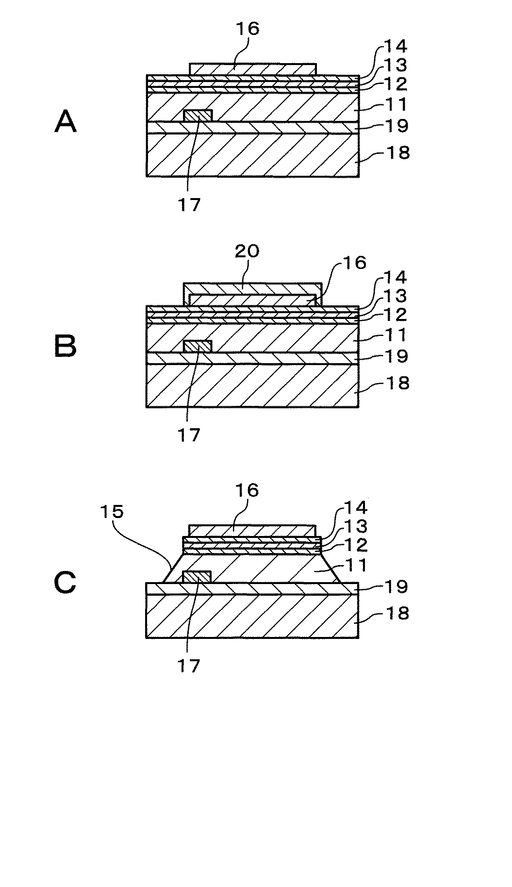
図1および図2に示すように、このGaN系発光ダイオードにおいては、n型GaN層11、その上のn型GaN層12、その上の例えば多重量子井戸(MQW)構造の発光層13およびその上のp型GaN層14により発光ダイオード構造が形成されている。n型GaN層11およびn型GaN層12には、n型不純物として例えばSiがドープされている。p型GaN層14には、p型不純物として例えばMgがドープされている。これらのn型GaN層11、n型GaN層12、発光層13およびp型GaN層14は全体として例えば円形の平面形状を有する。この場合、n型GaN層12、発光層13およびp型GaN層14は円柱形状を有する。また、n型GaN層11はテーパー形状を有し、その端面(側面)15はn型GaN層11の裏面(光取り出し面)に対して傾斜していて外部に光を取り出しやすくなっている。p型GaN層14上には、例えば円形のp側電極16が形成されている。n型GaN層11の裏面側には、このn型GaN層11に埋め込まれて金属電極からなるn側電極17が形成されている。このn側電極17のn型GaN層11に埋め込まれていない方の面とn型GaN層11の裏面とは互いにほぼ同一平面上にある。光取り出し効率を向上させるために、このn側電極17はn型GaN層11の裏面の外周部に近い位置に形成されている。典型的な一例では、n型GaN層11、n型GaN層12、発光層13およびp型GaN層14はC軸配向しており、n側電極17はn型GaN層11のC−面とコンタクトしている。
Hereinafter, embodiments of the present invention will be described with reference to the drawings. In addition, in FIGS. 1-15 of 1st-6th embodiment, the same code | symbol is attached | subjected to the same or corresponding part.
First, a first embodiment of the present invention will be described.
1 and 2 show a GaN-based light emitting diode according to the first embodiment. Here, FIG. 1 is a sectional view of the GaN-based light emitting diode, and FIG. 2 is a bottom view of the GaN-based light emitting diode.
As shown in FIGS. 1 and 2, in this GaN-based light emitting diode, an n-
n側電極17は、後述のように、基板上にあらかじめn側電極17を形成しておき、その上にn型GaN層11を成長させて覆うことにより、このn型GaN層11に埋め込むことができる。このn側電極17は、GaN系半導体層の高い成長温度(1000℃程度)に耐えられるように、例えば高融点金属であるRh(融点は1963℃)により形成するのが好ましい。Rhは可視光に対する反射率が77〜80%と高く、したがってn側電極17を高反射電極に構成することができる。このn側電極17は、n型GaN層11を成長させる際に良好な結晶性が得られるように、一方向の幅を例えば2μm以下に選ぶのが好ましいが、これに限定されるものではない。この場合、このn側電極17は、例えば幅2μm、長さ5μmの円弧状の平面形状を有する。ただし、このn側電極17の平面形状は円弧状に限定されず、他の形状、例えば長方形であってもよい。
As will be described later, the n-
n側電極17によって光取り出し面が一部遮光されるものの、このGaN系発光ダイオードにおいては、n側電極17が埋め込み電極であることに加えてn側電極17自体を高反射電極に構成することができることにより、発光層13からの光はn側電極17で反射されて方向が変化し、さらに端面15で反射されることによって外部に取り出される。したがって、このn側電極17は、必ずしも面積を小さくすることなく形成することが可能であり、例えば図3A〜Cに示すような繰り返しパターンからなる平面形状を有するn側電極17を用いてもよい。
図3Aはリング状の平面形状を有するn側電極17を示す。このn側電極17の幅は例えば1〜2μm程度であるが、これに限定されるものではない。
図3Bはメッシュ状のn側電極17を示す。このn側電極17においては、ほぼ等間隔の同心円状に配置された複数のリング状の部分と、これらのリング状の部分を接続するように放射状に配置された複数の直線状の部分とによりメッシュが構成されている。このn側電極17の各部の幅は例えば1〜2μm程度であるが、これに限定されるものではない。
図3Cはドット状のn側電極17を示す。このn側電極17においては、複数のドット状(円形)の電極がほぼ等間隔にグリッド状に配置されている。この場合、n側電極17は、n型GaN層11の裏面のほぼ全域に形成されている。各n側電極17の直径は例えば1〜2μm程度であるが、これに限定されるものではない。
これらの図3A〜Cに示したn側電極17においては、光取り出し効率を損なわずに、電流注入をほぼ均一に行うことが可能である。
Although the light extraction surface is partially shielded by the n-
FIG. 3A shows an n-
FIG. 3B shows the mesh-shaped n-
FIG. 3C shows the dot-shaped n-
In the n-
このGaN系発光ダイオードの各部の寸法、材料などの具体例を挙げると次のとおりである。n型GaN層11の厚さは例えば5μm、n型GaN層13の厚さは例えば200nm、発光層12の厚さは例えば200nm、p型GaN層13の厚さは例えば200nmである。発光層12は、例えば、InGaN井戸層とGaN障壁層とからなるMQW構造を有し、InGaN井戸層のIn組成は、このGaN系発光ダイオードが青色発光である場合は例えば0.17、緑色発光である場合は例えば0.25である。n型GaN層11に代えて、例えばn型InGaN層、n型AlGaN層およびn型GaN層を適宜組み合わせた積層構造とすることも可能である。また、p型GaN層13に代えて、例えばp型InGaN層、p型AlGaN層およびp型GaN層を適宜組み合わせた積層構造とすることも可能であり、この場合、好適には、p側電極16とコンタクトする部分はp型GaN層またはp型InGaN層とされる。発光ダイオード構造の最大径(n型GaN層11の裏面の最大径)は例えば20μm程度である。p側電極16は例えばNi/Ag/Au構造の金属多層膜からなり、Ni膜の厚さは例えば50nm、Ag膜の厚さは例えば50nm、Au膜の厚さは例えば2000nmである。p側電極16は、Ni/Au膜やAg/Au膜などからなるものであってもよい。n側電極17は例えばRh膜からなり、その厚さは例えば0.2μmである。
Specific examples of dimensions, materials, etc. of each part of the GaN-based light emitting diode are as follows. The thickness of the n-
このGaN系発光ダイオードにおいては、動作時に発光層13から発生する光は、端面15で反射されてn型GaN層11の裏面から外部に取り出され、あるいは、n側電極17および端面15で順次反射されて外部に取り出され、あるいは、直接n型GaN層11の裏面に向かってそのまま外部に取り出される。この場合、上述のようにn側電極17が埋め込み電極で、かつ高反射電極であることにより光取り出し効率の向上が図られているため、このGaN系発光ダイオードから外部に取り出される光の量を大きくすることができる。
In this GaN-based light emitting diode, light generated from the
次に、このGaN系発光ダイオードの製造方法について説明する。
図4Aに示すように、まず、例えば主面がC面のサファイア基板18を用意し、サーマルクリーニングを行うことなどによりその表面を清浄化した後、このサファイア基板18上に、例えば有機金属化学気相成長(MOCVD)法により、まず例えば500℃程度の低温で例えばGaNバッファ層(図示せず)を成長させ、その後1000℃程度まで昇温して結晶化させてから、その上にn型不純物として例えばSiがドープされたn型GaN層19を成長させる。このn型GaN層19の厚さは特に限定されないが、例えば2μm程度とする。このn型GaN層19は、平坦な表面を有するように成長させることができる。
Next, a method for manufacturing this GaN-based light emitting diode will be described.
As shown in FIG. 4A, first, for example, a
次に、n型GaN層19上にリソグラフィーにより所定形状のレジストパターン(図示せず)を形成し、さらに基板全面に、例えば真空蒸着法やスパッタリング法などによりRh膜を形成した後、このレジストパターンをその上に形成されたRh膜とともに除去する(リフトオフ)。これによって、n型GaN層19上にRhからなるn側電極17を形成する。
Next, a resist pattern (not shown) having a predetermined shape is formed on the n-
次に、図4Bに示すように、n側電極17が形成されたn型GaN層19上に、例えばMOCVD法により、n型不純物としてSiがドープされたn型GaN層11を成長させる。この際、n側電極17上にはn型GaN層11が直接成長しないが、n側電極17が成長マスクとなりn型GaN層11が横方向成長することにより、このn型GaN層11が成長するに連れてn側電極17を覆い始め、やがてこのn側電極17を完全に覆い尽くし、連続膜となる。例えば、n側電極17の幅が2μmの場合、n型GaN層11を例えば厚さ5μm程度成長させることでn側電極17を完全に覆うことができる。この場合、典型的な一例では、n型GaN層11はC軸方位で成長し、このn型GaN層11のC−面がn側電極17とコンタクトするようにする。こうすることで、この成長温度においてn型GaN層11とn側電極17との界面で合金化が起きやすく、n側電極17の良好なオーミックコンタクト特性を得ることができる。
Next, as shown in FIG. 4B, an n-
こうしてn側電極17をn型GaN層11で完全に覆った後、引き続いて、図4Cに示すように、n型不純物として例えばSiがドープされたn型GaN層12、発光層13およびp型不純物として例えばMgがドープされたp型GaN層14を順次成長させる。ここで、n型GaN層11およびn型GaN層12は例えば1020℃程度の温度で成長させ、発光層13は例えば600〜800℃程度の温度で成長させ、p型GaN層14は例えば800〜900℃程度の温度で成長させるが、これに限定されるものではない。また、n型GaN層11およびn型GaN層12は例えば水素ガス雰囲気中で成長させ、発光層13は例えば窒素ガス雰囲気中で成長させ、p型GaN層14は例えば水素ガス雰囲気中で成長させるが、これに限定されるものではない。
Thus, after completely covering the n-
上記のGaN系半導体層の成長原料は、例えば、Gaの原料としてはトリメチルガリウム((CH3 )3 Ga、TMG)、Alの原料としてはトリメチルアルミニウム((CH3 )3 Al、TMA)、Inの原料としてはトリメチルインジウム((CH3 )3 In、TMI)を、Nの原料としてはアンモニア(NH3 )を用いる。ドーパントについては、n型ドーパントとしては例えばシラン(SiH4 )を、p型ドーパントとしては例えばビス(メチルシクロペンタジエニル)マグネシウム((CH3 C5 H4 )2 Mg)あるいはビス(シクロペンタジエニル)マグネシウム((C5 H5 )2 Mg)を用いる。 For example, trimethylgallium ((CH 3 ) 3 Ga, TMG) is used as a raw material for Ga, and trimethylaluminum ((CH 3 ) 3 Al, TMA) is used as a raw material for Al. As a raw material, trimethylindium ((CH 3 ) 3 In, TMI) is used, and as a raw material of N, ammonia (NH 3 ) is used. As for the dopant, for example, silane (SiH 4 ) is used as the n-type dopant, and bis (methylcyclopentadienyl) magnesium ((CH 3 C 5 H 4 ) 2 Mg) or bis (cyclopentadi) is used as the p-type dopant. Enyl) magnesium ((C 5 H 5 ) 2 Mg) is used.
次に、上述のようにしてGaN系半導体層を成長させたサファイア基板18をMOCVD装置から取り出す。
次に、基板表面にリソグラフィーにより所定の円形のレジストパターン(図示せず)を形成し、さらに基板全面に例えば真空蒸着法により例えばNi膜、Ag膜およびAu膜を順次形成した後、このレジストパターンをその上に形成されたNi膜、Ag膜およびAu膜とともに除去する(リフトオフ)。これによって、図5に示すように、p型GaN層14上にNi/Ag/Au構造の円形のp側電極16を形成する。
Next, the
Next, a predetermined circular resist pattern (not shown) is formed on the surface of the substrate by lithography. Further, for example, a Ni film, an Ag film, and an Au film are sequentially formed on the entire surface of the substrate by, for example, a vacuum deposition method. Are removed together with the Ni film, Ag film and Au film formed thereon (lift-off). Thus, as shown in FIG. 5, a circular p-
次に、図5Bに示すように、p側電極16を含むp型GaN層14の所定領域の表面を覆う円形のレジストパターン20を形成する。
次に、レジストパターン20をマスクとして、例えば塩素系ガスをエッチングガスに用いたRIE法により、基板表面に対して垂直にエッチングが行われる条件でn型GaN層11に到達するまでエッチングを行い、引き続いて、テーパーエッチングが行われる条件でn型GaN層19に到達するまでエッチングを行った後、レジストパターン20を除去する。こうして、図6Cに示すように、n型GaN層12、発光層13およびp型GaN層14が円柱形状にパターニングされ、n型GaN層11が、そ下面に対して所定の角度傾斜した端面15を有するテーパー形状にパターニングされる。
Next, as shown in FIG. 5B, a circular resist
Next, etching is performed using the resist
次に、例えば、別の基板を用意し、この基板上にp側電極16を貼り合わせた後、サファイア基板18の裏面側から例えばエキシマーレーザなどによるレーザビームを照射してサファイア基板18とn型GaN層19との界面のアブレーションを行うことにより、n型GaN層19からサファイア基板18を剥離する(レーザ剥離)。次に、塩酸、王水、KOH、NaOHなどの酸またはアルカリ溶液により、剥離面に付着しているGaドロップレットを除去した後、剥離面の全体をRIE法によりエッチングして、この剥離面のGaNバッファ層および型GaN層19を除去し、最終的にn型GaN層11の裏面にn側電極17を露出させるとともにこの面を平坦化する。この時点で各GaN系発光ダイオード間が分離された状態となる。
Next, for example, another substrate is prepared, and the p-
必要に応じて、n型GaN層11の裏面を多少荒らすことにより、光取り出し効率の向上を図ることも可能である。例えば、n型GaN層11の裏面に、リソグラフィーおよびRIE法などによるエッチングにより、発光層13からの光を効率的に散乱することができる微小な凹凸(図示せず)を形成する。この凹凸の大きさおよび間隔は例えば0.1〜1μm程度である。この際、従来技術では、この凹凸の形成後にn側電極を形成していたため、そのコンタクト抵抗が高くなるという問題が生じるが、このGaN系発光ダイオードにおいては、すでにn側電極17が形成されているため、コンタクト特性が損なわれることがない。
If necessary, the light extraction efficiency can be improved by slightly roughening the back surface of the n-
この後、p側電極16側を貼り合わせた基板を除去して各GaN系発光ダイオードを分離する。
以上により、図1に示すように、目的とするGaN系発光ダイオードが完成する。こうして製造されたGaN系発光ダイオードは、用途に応じて、単体素子として用いてもよいし、他の基板と貼り合わせたり、転写したり、配線接続を行ったりすることができる。
図6AおよびBにこのGaN系発光ダイオードの実装例を示す。図6Aに示すように、例えば表面に所定形状の導電層が形成されたサブマウント21(例えば、熱放散性のよい銀メッキ銅やアルミナなどの高反射率のサブマウント)を用意し、その導電層に、図1に示すGaN系発光ダイオードのp側電極16を張り合わせる。そして、図6Bに示すように、例えば、図示省略した配線基板上に、光取り出し面であるn型GaN層11の裏面が上を向くようにサブマウント21を載せる。GaN系発光ダイオードのn側電極17と配線基板上に設けられた電極(図示せず)とをワイヤ22でボンディングするとともに、サブマウント21上に設けられ、GaN系発光ダイオードのp側電極16と電気的に接続されたパッド(図示せず)と配線基板上に設けられた別の電極(図示せず)とをワイヤー(図示せず)でボンディングする。そして、このGaN系発光ダイオードの全体を透明な樹脂23(輪郭のみ示す)によりモールドする。
Thereafter, the substrate on which the p-
As a result, the target GaN-based light emitting diode is completed as shown in FIG. The GaN-based light-emitting diode manufactured in this way may be used as a single element depending on the application, and can be bonded to another substrate, transferred, or connected to a wiring.
6A and 6B show an example of mounting this GaN-based light emitting diode. As shown in FIG. 6A, for example, a submount 21 (for example, a highly reflective submount such as silver-plated copper or alumina with good heat dissipation) having a conductive layer of a predetermined shape formed on the surface is prepared. The p-
図7に、このGaN系発光ダイオードを樹脂パッケージ化し配線接続した例を示す。図7に示すように、GaN系発光ダイオードの側面を樹脂24で覆い、p側電極16上に対応する部分にバンプ25を形成する。パッケージの下面にはn側電極17に接続するようにITO(インジウム−スズ酸化物)のような透明電極26を形成する。この透明電極26は例えばITOインクを塗布し、乾燥することによって形成する。このようにパッケージ化されたGaN系発光ダイオードを、例えば配線基板の面内に規則的に配列した後、p側電極16上に形成されたバンプ25に接続した配線27と、n側電極17を覆うように形成した透明配線26とを用いて、複数のGaN系発光ダイオードを接続することができる。
FIG. 7 shows an example in which this GaN-based light emitting diode is formed into a resin package and connected by wiring. As shown in FIG. 7, the side surface of the GaN-based light emitting diode is covered with a
以上のように、この第1の実施形態によれば、n側電極17が、この上に成長させたn型GaN層11に埋め込まれていることにより、n型GaN層11に対するn側電極17のコンタクト抵抗の低減を図ることができ、n側電極17のコンタクトを良好に取ることができるので、GaN系発光ダイオードの動作電圧の低減を図ることができる。また、n側電極17が埋め込み電極であり、かつ高反射電極であることにより、光取り出し効率の向上を図ることができ、発光効率の向上を図ることができる。
As described above, according to the first embodiment, since the n-
次に、この発明の第2の実施形態について説明する。
図8はこの第2の実施形態によるGaN系発光ダイオードの製造方法を説明するための断面図である。
この第2の実施形態においては、第1の実施形態と同様にしてサファイア基板18上にn型GaN層19を成長させる工程まで行った後、このn型GaN層19上に、例えばCVD法によりSiO2 膜を形成する。このSiO2 膜の厚さは例えば100nm程度である。次に、このSiO2 膜上にリソグラフィーにより所定形状のレジストパターン(図示せず)を形成し、さらに基板全面に例えば真空蒸着法により例えばRh膜を形成した後、このレジストパターンをその上に形成されたRh膜とともに除去する(リフトオフ)。これにより、図8Aに示すように、Rh膜からなるn側電極17が形成される。次に、このn側電極17をマスクとしてその下のSiO2 膜をエッチングすることによりこのn側電極17と同一形状にパターニングする。SiO2 膜28に代えてSiN膜を形成してもよい。次に、第1の実施形態と同様にして、n側電極17およびSiO2 膜28を成長マスクとして、n側電極17を覆うようにn型GaN層11を成長させる。この際、n型GaN層19とn側電極17との間にSiO2 膜28が挿入されており、n型GaN層19とn側電極17とが直接接触していないので、n型GaN層11の成長時に、n側電極17を構成するRhによる触媒効果により下地のn型GaN層19が気相エッチングで削られるのを防止することができる。
Next explained is the second embodiment of the invention.
FIG. 8 is a cross-sectional view for explaining a GaN-based light emitting diode manufacturing method according to the second embodiment.
In the second embodiment, the process up to the growth of the n-
この後、第1の実施形態と同様に、n型GaN層12、発光層13およびp型GaN層14を成長させ、サファイア基板18を剥離し、剥離面に付着しているGaドロップレットを除去した後、剥離面のGaNバッファ層およびn型GaN層19を除去し、必要に応じて例えばフッ酸系エッチャントを用いたウエットエッチングを行ってSiO2 膜28を除去し、最終的にn型GaN層11の下面にn側電極17を露出させるとともにこの面を平坦化する。この状態を図8Dに示す。
上記以外のことは第1の実施形態と同様である。
この第2の実施形態によれば、第1の実施形態と同様な利点を得ることができる。
Thereafter, as in the first embodiment, the n-
Other than the above are the same as in the first embodiment.
According to the second embodiment, the same advantages as those of the first embodiment can be obtained.
次に、この発明の第3の実施形態について説明する。
図9はこの第3の実施形態によるGaN系発光ダイオードの製造方法を説明するための断面図である。
この第3の実施形態においては、第1の実施形態と同様にして図4Aに示す工程まで行った後、図9Aに示すように、n側電極17が形成されたn型GaN層19の全面に、まず、例えば600℃程度の低い温度で、n型GaN層11を例えば50nm程度の厚さ成長させる。このとき、n側電極17上には多結晶状のn型GaN層29が成長する。こうしてn型GaN層29でn側電極17を完全に覆い尽くす。引き続いて、成長温度を例えば1020℃に昇温してn型GaN層11をさらに成長させる。このとき、多結晶状のn型GaN層29が上方に伸びるが、周囲から横方向成長したn型GaN層11によってこのn型GaN層29が覆われていき、n型GaN層11を例えば5〜10μm程度の厚さ成長させることにより、n側電極17上のn型GaN層29を完全に覆うことができ、n型GaN層11が結晶性が良好な連続膜となる。このようにn型GaN層11を成長させることにより、n側電極17の上側にボイドが形成されるのを防止することができる。また、n側電極17上に成長するn型GaN層29では多結晶状となるが、導電型がn型のため十分にコンタクト抵抗を低くすることができる。
この後、図9B〜図9Dに示すように、第1の実施形態と同様に工程を進めて目的とするGaN系発光ダイオードを製造する。
この第3の実施形態によれば、第1の実施形態と同様の利点を得ることができる。
Next explained is the third embodiment of the invention.
FIG. 9 is a cross-sectional view for explaining a GaN-based light emitting diode manufacturing method according to the third embodiment.
In the third embodiment, the process up to the step shown in FIG. 4A is performed in the same manner as the first embodiment, and then the entire surface of the n-
Thereafter, as shown in FIG. 9B to FIG. 9D, the target GaN-based light emitting diode is manufactured through the same process as in the first embodiment.
According to the third embodiment, the same advantages as those of the first embodiment can be obtained.
次に、この発明の第4の実施形態について説明する。
図10はこの第4の実施形態によるGaN系発光ダイオードを示す。
図10に示すように、このGaN系発光ダイオードは、n側電極17のn型GaN層11に埋め込まれている側の面30が、n型GaN層11の裏面(光取り出し面)およびn側電極17の露出している側の面(表面)に対して傾斜していることを除いて、第1の実施形態によるGaN系発光ダイオードと同様な構造を有する。この場合、n側電極17は、中央部が高く、その両側の周辺部が低い、三角形の形状の断面を有する。n側電極17のn型GaN層11に埋め込まれている側の面が、光取り出し面(この場合、n型GaN層11の裏面)に平行になっていると、内部を伝播する光を外部に取り出しにくいが、このn側電極17においては、光取り出し面と平行な面は表面の面のみで、n型GaN層11に埋め込まれている側の面30は光取り出し面に対して傾斜しており、この面30で光を反射させることで内部を伝播する光を外部に取り出しやすくなるため、光取り出し効率を高くすることができる。
Next explained is the fourth embodiment of the invention.
FIG. 10 shows a GaN-based light emitting diode according to the fourth embodiment.
As shown in FIG. 10, in this GaN-based light emitting diode, the
このGaN系発光ダイオードを製造するには、第1の実施形態と同様にして図4Aに示すように長方形断面のn側電極17を形成する工程まで行った後、全面にレジストを塗布し、このレジストをリフローすることによりn側電極17を形成する部分の中央部を高く、周辺部を低くする。次に、例えばRIE法により全面をエッチングすることにより、図11Aに示すように、三角形の形状の断面を有するn側電極17を形成することができる。
この後、図11B、Cおよび図10に示すように、第1の実施形態と同様に工程を進めて目的とするGaN系発光ダイオードを製造する。
この第4の実施形態によれば、第1の実施形態と同様の利点を得ることができる。
In order to manufacture this GaN-based light emitting diode, the process is performed up to the step of forming the n-
Thereafter, as shown in FIGS. 11B, 11C, and 10, the process proceeds in the same manner as in the first embodiment to manufacture the target GaN-based light emitting diode.
According to the fourth embodiment, the same advantages as those of the first embodiment can be obtained.
次に、この発明の第5の実施形態について説明する。
図12はこの第5の実施形態によるGaN系発光ダイオードを示す。
図12に示すように、このGaN系発光ダイオードにおいては、n側電極17の上面とn型GaN層11との間に、活性層13からの光を反射する誘電体膜として、例えばSiO2 膜32が設けられていることを除いて、第1の実施形態によるGaN系発光ダイオードと同様な構造を有する。このSiO2 膜32の厚さは例えば100nmである。この場合、n側電極17は上面ではn型GaN層11とコンタクトせず、両側面でしかn型GaN層11とコンタクトしないため、n側電極17のコンタクト抵抗を低くし、良好なコンタクトを取ることができるようにする観点から、n側電極17の厚さは例えば0.2〜2μm程度とする。
このGaN系発光ダイオードにおいては、n側電極17の上面とn型GaN層11との間にSiO2 膜32が設けられていることにより、n側電極17とn型GaN層11とが直接接触する界面が大きく減少し、活性層13からの光はSiO2 膜32で全反射するようになるので、このn側電極17はいわゆるODR電極となり、光取り出し効率の大幅な向上を図ることができる。
Next explained is the fifth embodiment of the invention.
FIG. 12 shows a GaN-based light emitting diode according to the fifth embodiment.
As shown in FIG. 12, in this GaN-based light emitting diode, as a dielectric film for reflecting light from the
In this GaN-based light emitting diode, since the SiO 2 film 32 is provided between the upper surface of the n-
このGaN系発光ダイオードを製造するには、第1の実施形態と同様にしてサファイア基板18上にn型GaN層19を成長させる工程まで行った後、このn型GaN層19上に、例えばCVD法によりSiO2 膜を形成する。このSiO2 膜の厚さは例えば100nm程度である。次に、例えば真空蒸着法やスパッタリング法などにより、このSiO2 膜上にRh膜を形成する。次に、このRh膜上に、例えばCVD法によりSiO2 膜を形成する。次に、リソグラフィーにより所定形状のレジストパターン(図示せず)を形成した後、このレジストパターンをマスクとしてこれらのSiO2 膜、Rh膜およびSiO2 膜を順次エッチングする。これにより、図13Aに示すように、SiO2 膜28、n側電極17およびSiO2 膜32の積層構造が形成される。この際、n型GaN層19とn側電極17との間にSiO2 膜28が挿入されており、n型GaN層19とn側電極17とが直接接触していないので、n型GaN層11の成長時に、n側電極17を構成するRhによる触媒効果により下地のn型GaN層19が気相エッチングで削られるのを防止することができる。
In order to manufacture this GaN-based light emitting diode, after the process up to the growth of the n-
次に、図13Bに示すように、第1の実施形態と同様にして、SiO2 膜28、n側電極17およびSiO2 膜32を成長マスクとして、SiO2 膜32を覆うようにn型GaN層11を成長させる。
この後、第2の実施形態と同様に工程を進めて、図12に示す目的とするGaN系発光ダイオードを製造する。
この第5の実施形態によれば、第1および第2の実施形態と同様の利点を得ることができる。
Next, as shown in FIG. 13B, similarly to the first embodiment, the n-type GaN is formed so as to cover the SiO 2 film 32 using the SiO 2 film 28, the n-
Thereafter, the process proceeds in the same manner as in the second embodiment, and the target GaN-based light emitting diode shown in FIG. 12 is manufactured.
According to the fifth embodiment, the same advantages as those of the first and second embodiments can be obtained.
次に、この発明の第6の実施形態について説明する。
図14A〜Dは、この第6の実施形態によるGaN系発光ダイオードの製造方法を説明するための断面図である。
このGaN系発光ダイオードの製造方法においては、図14Aに示すように、第1の実施形態と同様にして図4Aに示す工程まで行う。このとき、n側電極17は、例えばRh膜およびNi膜を順次積層することにより形成する。次に、p型GaN層14上に所定形状のレジストパターン形成した後、このレジストパターンをマスクとして例えばRIE法によりサファイア基板18が露出するまでエッチングを行う。これにより、図14Bに示すように、各GaN系発光ダイオード間が分離された状態となる。
Next, a sixth embodiment of the present invention will be described.
14A to 14D are cross-sectional views for explaining a method for manufacturing a GaN-based light emitting diode according to the sixth embodiment.
In this method of manufacturing a GaN-based light emitting diode, as shown in FIG. 14A, the steps up to the step shown in FIG. 4A are performed in the same manner as in the first embodiment. At this time, the n-
次に、図14Cに示すように、p型GaN層14上の所定部分に、例えばリフトオフにより例えばNi/Au/Ag構造のp側電極16を形成する。次に、p側電極16をマスクとして、例えばRIE法によりn側電極17が露出するまでエッチングを行う。このとき、n側電極17の最表面が、RIE法によりエッチングされにくいNi膜となっているため、n側電極17が過度にエッチングされることなくエッチングを停止することができる。
以上により、目的とするGaN系発光ダイオードが製造される。
Next, as shown in FIG. 14C, a p-
Thus, the target GaN-based light emitting diode is manufactured.
図15に、このGaN系発光ダイオードをフリップチップ実装した場合の例を示す。図15に示すように、p側電極16およびn側電極17に、例えば熱放散性のよい銀メッキ銅や、アルミナなどの高反射のサブマウント33およびサブマウント34をそれぞれを取り付け、サファイア基板18が上側にくるように段差のあるパッケージに取り付けることで電極を外部に取り出す。
サファイア基板18は取り付けたままでもよいが、必要に応じて、サファイア基板18の裏面側からレーザビームを照射して、サファイア基板18をn型GaN層19から剥離してもよい。この場合、光取り出し効率の向上の観点から、n型GaN層19の下面に、ウエットエッチングを行ったり、リソグラフィーおよびRIE法などによるエッチングを行ったりして、発光波長の光を効率的に散乱することができる微小な凹凸(図示せず)を形成してもよい。
FIG. 15 shows an example in which this GaN-based light emitting diode is flip-chip mounted. As shown in FIG. 15, a high-
The
この第6の実施形態によれば、基板上にあらかじめn側電極17を形成しておき、このn側電極17を埋め込むように発光ダイオード構造を形成するGaN系半導体層を成長させ、その後、成長面側から発光ダイオード構造を形成するGaN系半導体層の一部をエッチングすることによりn側電極17を露出するようにしているため、片面にp側電極16およびn側電極17を有するGaN系発光ダイオードを容易に製造することができる。
According to the sixth embodiment, the n-
次に、この発明の第7の実施形態について説明する。
この第7の実施形態においては、発光層13の構成が第1の実施形態と異なる。具体的には、発光層13は複数の井戸層を含むMQW構造を有し、この発光層13のn型GaN層12側の井戸層密度をd1 、p型GaN層14側の井戸層密度をd2 としたとき、d1 <d2 を満足するように発光層13における井戸層が配置されている。このように発光層13における井戸層密度を異ならせるためには、例えば、井戸層の厚さを一定とし、障壁層の厚さを異ならせる(具体的には、発光層13におけるp型GaN層14側の障壁層の厚さを、n型GaN層12側の障壁層の厚さよりも小さくする)のが好ましいが、これに限定されるものではなく、障壁層の厚さを一定とし、井戸層の厚さを異ならせる(具体的には、発光層13におけるp型GaN層14側の井戸層の厚さを、n型GaN層12側の井戸層の厚さよりも大きくする)ようにしてよいし、井戸層の厚さおよび障壁層の厚さの両方を異ならせてもよい。ここで、1<d2 /d1 ≦20、好ましくは1.2≦d2 /d1 ≦10、より好ましくは1.5≦d2 /d1 ≦5を満足するように、発光層13における井戸層が配置される。
Next explained is the seventh embodiment of the invention.
In the seventh embodiment, the configuration of the
発光層13が9層の井戸層および8層の障壁層からなるMQW構造を有する緑色発光のGaN系発光ダイオードを作製し、このGaN系発光ダイオードを発光させた場合に発光層13の各井戸層からの発光割合がどのようになっているかを視覚化する実験を行った。このGaN系発光ダイオードにおいては、n型GaN層12の厚さは3μm、p型GaN層14の厚さは120nmであり、n型GaN層12と発光層13との間およびp型GaN層14と発光層13との間にはそれぞれ厚さ5nmのアンドープGaN層が設けられている。発光層13における井戸層は厚さ3nmのIn0.23Ga0.77N層からなり、障壁層は厚さ15nmのGaN層からなる。このGaN系発光ダイオード(試料1)においては動作電流密度60A/cm2 での発光ピーク波長が515nmであり、発光効率は180mW/Aであった。
A green light emitting GaN-based light-emitting diode having an MQW structure in which the light-emitting
次に、試料1のGaN系発光ダイオードと同様の層構造を有するが、発光層13における9層の井戸層のうちの特定の1層のみ厚さ3nmのIn0.15Ga0.85N層としたGaN系発光ダイオードを作製した。n型GaN層12側から第1番目の井戸層がIn0.15Ga0.85N層であるGaN系発光ダイオードを試料2、第3番目の井戸層がIn0.15Ga0.85N層であるGaN系発光ダイオードを試料3、第5番目の井戸層がIn0.15Ga0.85N層であるGaN系発光ダイオードを試料4、第7番目の井戸層がIn0.15Ga0.85N層であるGaN系発光ダイオードを試料5、第9番目の井戸層がIn0.15Ga0.85N層であるGaN系発光ダイオードを試料6と呼ぶ。これらの試料2〜6のGaN系発光ダイオードにおいては、他の井戸層は上述のように厚さ3nmのIn0.23Ga0.77N層からなる。これらの試料2〜6のGaN系発光ダイオードにおいても、動作電流密度60A/cm2 での発光ピーク波長が515nmであり、発光効率は180mW/Aであった。しかしながら、いくつかの試料では、緑色の発光(発光波長約515nm)以外に、In0.15Ga0.85N層からなる井戸層の存在に起因して、青色の発光領域(発光波長約450nm)にも小さな発光ピークが見られた。この青色の発光ピーク成分の全体に占める割合を図16にプロットした。図16の横軸の第1層目、第3層目、…はIn0.15Ga0.85N層からなる井戸層のn型GaN層12側からの位置を示す。図16の横軸の第N層目(N=1、3、5、7、9)に該当する青色の発光ピーク成分の全体に占める割合のデータは、発光層13における第N層目の井戸層がIn0.15Ga0.85N層からなるGaN系発光ダイオードにおける青色の発光ピーク成分の全体に占める割合の動作電流密度毎のデータを示す。
Next, the GaN-based light-emitting diode has a layer structure similar to that of the GaN-based light-emitting diode of
図16から明らかなように、発光はどの動作電流密度においても、MQW構造を有する発光層13におけるp型GaN層14側、発光層13の厚さ方向約2/3の領域に偏っている。また、発光の80%は、p型GaN層14側の発光層13の厚さ方向1/2までの領域からの発光で占められている。このように発光が著しく偏る理由として、電子および正孔の移動度の違いが挙げられる。GaN系化合物半導体においては正孔の移動度が小さいため、正孔はp型GaN層14の近傍の発光層13の井戸層までしか到達せず、正孔と電子との再結合による発光がp型GaN層14側に偏ると考えられる。また、井戸層と障壁層とからなるヘテロ障壁のキャリアに対する透過率という点でも、有効質量の大きな正孔は複数の障壁層を越えてn型GaN層12側の発光層13の井戸層まで到達することが困難であるという要因も考えられる。
このことから、p型GaN層14側に偏った発光を有効に利用するためには、井戸層の分布をp型GaN層14側に偏らせた非対称分布の井戸層を有するMQW構造を採用することが有効である。さらに、発光分布のピークは、p型GaN層14側の発光層13の厚さ方向1/3〜1/4の領域に位置していることが分かる。
As is apparent from FIG. 16, light emission is biased to a region of about 2/3 of the
Therefore, in order to effectively use the light that is biased toward the p-
実施例について説明する。
実施例1のGaN系発光ダイオードは、発光層13の構成および構造を除いて試料1のGaN系発光ダイオードと同様の構成を有する。
発光層13を構成するMQW構造の詳細を表1に示す。なお、表1あるいは後述する表2中、井戸層の厚さおよび障壁層の厚さの値の右側の括弧内の数字は、発光層13におけるn型GaN層13側の界面(より具体的には、実施例1においてはアンドープGaN層と発光層13との界面)からの積算厚さを示す。
Examples will be described.
The GaN-based light emitting diode of Example 1 has the same configuration as the GaN-based light emitting diode of
Details of the MQW structure constituting the
実施例1においては、発光層13の総厚をt0 とし、発光層13におけるn型GaN層12側の界面(より具体的には、実施例1においてはアンドープGaN層と発光層13との界面)から厚さ(2t0 /3)までの発光層13の第1領域内の井戸層密度をd1 、p型GaN層14側の界面(より具体的には、実施例1においてはアンドープGaN層と発光層13との界面)から厚さ(t0 /3)までの発光層13の第2領域内の井戸層密度をd2 としたとき、d1 <d2 を満足するように発光層13における井戸層が配置されている。
In Example 1, the total thickness of the
具体的には、井戸層密度d1 および井戸層密度d2 を式(1)、(2)から求めると、以下のとおりとなる。
〈実施例1〉
d2 =(WL2 /WL)/(t2 /t0 )
=(4/10)/(50/150)
=1.20
d1 =(WL1 /WL)/(t1 /t0 )
=(6/10)/(100/150)
=0.90
Specifically, when the well layer density d 1 and the well layer density d 2 are obtained from the equations (1) and (2), they are as follows.
<Example 1>
d 2 = (WL 2 / WL) / (t 2 / t 0 )
= (4/10) / (50/150)
= 1.20
d 1 = (WL 1 / WL) / (t 1 / t 0 )
= (6/10) / (100/150)
= 0.90
比較のために、表1に比較例1として示す発光層13を有するGaN系発光ダイオードを作製した。
実施例1および比較例1のGaN系発光ダイオードにおいては、発光層13の面積(接合領域の面積)を6×10⁻⁴cm2 とした。したがって、GaN系発光ダイオードの動作電流密度は、動作電流値を6×10⁻⁴cm2 で除した値となる。例えば、20mAの駆動電流を流した場合の動作電流密度は33A/cm2 となる。
比較例1における井戸層密度d1 および井戸層密度d2 を式(1)、(2)から求めると、以下のとおりとなる。
〈比較例1〉
d2 =(WL2 /WL)/(t2 /t0 )
={(3+1/3)/10}/(49/147)
=1.00
d1 =(WL1 /WL)/(t1 /t0 )
={(6+2/3)}/10}/(98/147)
=1.00
For comparison, a GaN-based light emitting diode having the
In the GaN-based light emitting diodes of Example 1 and Comparative Example 1, the area of the light emitting layer 13 (area of the junction region) was 6 × 10 −4 cm 2 . Therefore, the operating current density of the GaN-based light emitting diode is a value obtained by dividing the operating current value by 6 × 10 −4 cm 2 . For example, the operating current density when a drive current of 20 mA is applied is 33 A / cm 2 .
When the well layer density d 1 and the well layer density d 2 in Comparative Example 1 are obtained from the equations (1) and (2), they are as follows.
<Comparative example 1>
d 2 = (WL 2 / WL) / (t 2 / t 0 )
= {(3 + 1/3) / 10} / (49/147)
= 1.00
d 1 = (WL 1 / WL) / (t 1 / t 0 )
= {(6 + 2/3)} / 10} / (98/147)
= 1.00
GaN系発光ダイオードの動作電流密度と光出力との関係を測定した結果を図17に示すが、実施例1のGaN系発光ダイオードの光出力は比較例1よりも増加している。そして、実施例1のGaN系発光ダイオードと比較例1のGaN系発光ダイオードとの光出力の差は、動作電流密度が50A/cm2 以上で顕著となり、動作電流密度が100A/cm2 以上では1割以上の差となる。すなわち、実施例1のGaN系発光ダイオードは、動作電流密度が50A/cm2 以上、好ましくは動作電流密度が100A/cm2 以上で、比較例1のGaN系発光ダイオードよりも光出力が大きく増加するので、動作電流密度が50A/cm2 以上、好ましくは動作電流密度が100A/cm2 以上での使用が望ましいといえる。 FIG. 17 shows the result of measuring the relationship between the operating current density of the GaN-based light emitting diode and the light output. The light output of the GaN-based light emitting diode of Example 1 is higher than that of Comparative Example 1. The difference in light output between the GaN-based light emitting diode of Example 1 and the GaN-based light emitting diode of Comparative Example 1 becomes significant when the operating current density is 50 A / cm 2 or more, and when the operating current density is 100 A / cm 2 or more. The difference is 10% or more. That is, the GaN-based light emitting diode of Example 1 has an operating current density of 50 A / cm 2 or more, preferably 100 A / cm 2 or more, and the light output is significantly increased compared to the GaN-based light emitting diode of Comparative Example 1. Therefore, it can be said that it is desirable to use an operating current density of 50 A / cm 2 or more, preferably 100 A / cm 2 or more.
さらには、GaN系発光ダイオードの動作電流密度と発光ピーク波長との関係を図18に示す。動作電流密度を0.1A/cm2 から300A/cm2 へと増加させると、比較例1ではΔλ=−19nmであるのに対して、実施例1ではΔλ=−8nmと、小さな発光波長シフトが実現されている。特に、動作電流密度が30A/cm2 以上では、ほとんど波長シフトが観測されない。言い換えれば、動作電流密度を30A/cm2 以上とする場合、発光波長の変化がわずかしか生じないので、発光波長や発光色の管理の面で好ましい。特に、動作電流密度が50A/cm2 以上、あるいは100A/cm2 以上においては、実施例1のGaN系発光ダイオードは、比較例1のGaN系発光ダイオードよりも顕著に波長シフトが小さく、優位性が明らかである。 Furthermore, FIG. 18 shows the relationship between the operating current density of the GaN-based light emitting diode and the emission peak wavelength. When the operating current density is increased from 0.1 A / cm 2 to 300 A / cm 2 , Δλ = −19 nm in Comparative Example 1, whereas Δλ = −8 nm in Example 1, a small emission wavelength shift. Is realized. In particular, when the operating current density is 30 A / cm 2 or more, almost no wavelength shift is observed. In other words, when the operating current density is 30 A / cm 2 or more, the light emission wavelength changes only slightly, which is preferable in terms of management of the light emission wavelength and the light emission color. In particular, when the operating current density is 50 A / cm 2 or more, or 100 A / cm 2 or more, the GaN-based light-emitting diode of Example 1 has a significantly smaller wavelength shift than the GaN-based light-emitting diode of Comparative Example 1, and is superior. Is clear.
なお、このようなGaN系発光ダイオードの発光量(輝度)の制御は駆動電流のピーク電流値で行う方法に加えて、駆動電流のパルス幅制御で行ってもよいし、駆動電流のパルス密度制御で行ってもよいし、これらの組合せで行ってもよい。
なお、発光層13の総厚をt0 とし、発光層13におけるn型GaN層12側の界面(より具体的には、アンドープGaN層と発光層13との界面)から厚さ(t0 /2)までの発光層13の第1領域内の井戸層密度をd1 、p型GaN層14側の界面(より具体的には、アンドープGaN層と発光層13との界面)から厚さ(t0 /2)までの発光層13の第2領域内の井戸層密度をd2 としたとき、d1 <d2 を満足するように発光層13における井戸層が配置されているとした場合の、井戸層密度d1 および井戸層密度d2 を式(1)、(2)から求めると、以下のとおりとなる。
In addition to the method of controlling the light emission amount (luminance) of the GaN-based light emitting diode based on the peak current value of the driving current, it may be performed by controlling the pulse width of the driving current or controlling the pulse density of the driving current. It may be carried out by a combination of these.
Note that the total thickness of the
〈実施例1相当〉
d2 =(WL2 /WL)/(t2 /t0 )
=(6/10)/(75/150)
=1.20
d1 =(WL1 /WL)/(t1 /t0 )
=(4/10)/(75/150)
=0.80
<Equivalent to Example 1>
d 2 = (WL 2 / WL) / (t 2 / t 0 )
= (6/10) / (75/150)
= 1.20
d 1 = (WL 1 / WL) / (t 1 / t 0 )
= (4/10) / (75/150)
= 0.80
〈比較例1相当〉
d2 =(WL2 /WL)/(t2 /t0 )
=(5/10)/{(73+1/2)/147}
=1.00
d1 =(WL1 /WL)/(t1 /t0 )
=(5/10)/{(73+1/2)/147}
=1.00
<Comparative example 1 equivalent>
d 2 = (WL 2 / WL) / (t 2 / t 0 )
= (5/10) / {(73 + 1/2) / 147}
= 1.00
d 1 = (WL 1 / WL) / (t 1 / t 0 )
= (5/10) / {(73 + 1/2) / 147}
= 1.00
また、発光層13の総厚をt0 とし、発光層13におけるn型GaN層12側の界面(より具体的には、アンドープGaN層と発光層13との界面)から厚さ(t0 /3)までの発光層13の第1領域内の井戸層密度をd1 、p型GaN層14側の界面(より具体的には、アンドープGaN層と発光層13との界面)から厚さ(2t0 /3)までの発光層13の第2領域内の井戸層密度をd2 としたとき、d1 <d2 を満足するように発光層13における井戸層が配置されているとした場合の、井戸層密度d1 および井戸層密度d2 を式(1)、(2)から求めると、以下のとおりとなる。
Further, the total thickness of the
〈実施例1相当〉
d2 =(WL2 /WL)/(t2 /t0 )
=(8/10)/(50/150)
=2.40
d1 =(WL1 /WL)/(t1 /t0 )
=(2/10)/(100/150)
=0.30
<Equivalent to Example 1>
d 2 = (WL 2 / WL) / (t 2 / t 0 )
= (8/10) / (50/150)
= 2.40
d 1 = (WL 1 / WL) / (t 1 / t 0 )
= (2/10) / (100/150)
= 0.30
〈比較例1相当〉
d2 =(WL2 /WL)/(t2 /t0 )
={(6+2/3)/10}/(98/147)
=1.00
d1 =(WL1 /WL)/(t1 /t0 )
={(3+1/3)/10}/(49/147)
=1.00
以上のように、いずれの場合においても、実施例1に相当する場合、d1 <d2 を満足するように発光層13における井戸層が配置されている。
<Comparative example 1 equivalent>
d 2 = (WL 2 / WL) / (t 2 / t 0 )
= {(6 + 2/3) / 10} / (98/147)
= 1.00
d 1 = (WL 1 / WL) / (t 1 / t 0 )
= {(3 + 1/3) / 10} / (49/147)
= 1.00
As described above, in any case, in the case corresponding to Example 1, the well layer in the
次に、実施例2について説明する。この実施例2は実施例1の変形である。実施例2のGaN系発光ダイオードにおいては、発光層13の井戸層のIn組成比を調整して発光波長を約445nmとした。この実施例2のGaN系発光ダイオードにおける発光層13を構成するMQW構造の詳細を表2に示す。
Next, Example 2 will be described. The second embodiment is a modification of the first embodiment. In the GaN-based light emitting diode of Example 2, the emission wavelength was set to about 445 nm by adjusting the In composition ratio of the well layer of the
井戸層密度d1 および井戸層密度d2 を式(1)、(2)から求めると、以下のとおりとなる。
〈実施例2〉
d2 =(WL2 /WL)/(t2 /t0 )
={(5+2/9)/10}/{(40+2/3)/122}
=1.57
d1 =(WL1 /WL)/(t1 /t0 )
={(4+7/9)/10}/{(81+1/3)/122}
=0.72
When the well layer density d 1 and the well layer density d 2 are obtained from the equations (1) and (2), they are as follows.
<Example 2>
d 2 = (WL 2 / WL) / (t 2 / t 0 )
= {(5 + 2/9) / 10} / {(40 + 2/3) / 122}
= 1.57
d 1 = (WL 1 / WL) / (t 1 / t 0 )
= {(4 + 7/9) / 10} / {(81 + 1/3) / 122}
= 0.72
比較のために、表2に比較例2として示す発光層13を有するGaN系発光ダイオードを作製した。比較例2における井戸層密度d1 および井戸層密度d2 を式(1)、(2)から求めると、以下のとおりとなる。
〈比較例2〉
d2 =(WL2 /WL)/(t2 /t0 )
={(3+1/3)/10}/{(41+1/2)/(124+1/2)}
=1.00
d1 =(WL1 /WL)/(t1 /t0 )
={(6+2/3)}/10}/{83/(124+1/2)}
=1.00
そして、実施例2および比較例2のGaN系発光ダイオードを、実施例1と同様の方法により評価した。
For comparison, a GaN-based light emitting diode having a
<Comparative example 2>
d 2 = (WL 2 / WL) / (t 2 / t 0 )
= {(3 + 1/3) / 10} / {(41 + 1/2) / (124 + 1/2)}
= 1.00
d 1 = (WL 1 / WL) / (t 1 / t 0 )
= {(6 + 2/3)} / 10} / {83 / (124 + 1/2)}
= 1.00
The GaN-based light emitting diodes of Example 2 and Comparative Example 2 were evaluated by the same method as in Example 1.
GaN系発光ダイオードの動作電流密度と発光ピーク波長との関係を図19に示す。動作電流密度を0.1A/cm2 から300A/cm2 へと増加させると、比較例1ではΔλ=−9nmであるのに対して、実施例2ではΔλ=−1nmと、極めて小さな発光波長シフトが実現されている。このように、青色を発光する実施例2のGaN系発光ダイオードは、比較例2のGaN系発光ダイオードよりも顕著に波長シフトが小さく、優位性が明らかである。
この第7の実施形態によれば、第1の実施形態と同様な利点に加えて、動作電流密度の増加に伴う発光波長の大きなシフトを抑制することができ、しかも一層広範囲の輝度制御を行うことができるという利点を得ることができる。
FIG. 19 shows the relationship between the operating current density of the GaN-based light emitting diode and the emission peak wavelength. When the operating current density is increased from 0.1 A / cm 2 to 300 A / cm 2 , Δλ = −9 nm in Comparative Example 1, whereas Δλ = −1 nm in Example 2, which is an extremely small emission wavelength. Shift is realized. Thus, the GaN-based light-emitting diode of Example 2 that emits blue light has a significantly smaller wavelength shift than the GaN-based light-emitting diode of Comparative Example 2, and the superiority is clear.
According to the seventh embodiment, in addition to the same advantages as those of the first embodiment, it is possible to suppress a large shift in the emission wavelength accompanying an increase in operating current density, and to perform a wider range of luminance control. The advantage that it can be obtained.
以上、この発明の実施形態について具体的に説明したが、この発明は、上述の実施形態に限定されるものではなく、この発明の技術的思想に基づく各種の変形が可能である。
例えば、上述の第1〜第7の実施形態において挙げた数値、材料、構造、形状、基板、原料、プロセスなどはあくまでも例に過ぎず、必要に応じて、これらと異なる数値、材料、構造、形状、基板、原料、プロセスなどを用いてもよい。
As mentioned above, although embodiment of this invention was described concretely, this invention is not limited to the above-mentioned embodiment, The various deformation | transformation based on the technical idea of this invention is possible.
For example, the numerical values, materials, structures, shapes, substrates, raw materials, processes and the like given in the first to seventh embodiments are merely examples, and if necessary, numerical values, materials, structures, Shapes, substrates, raw materials, processes, etc. may be used.
また、上述の第1〜第5の実施形態において、n側電極17として最表面がNiからなる金属多層膜、具体的には、例えばRh/Ni構造の金属多層膜を用いてもよい。この場合、n側電極17は、n型GaN層19上にNi膜およびRh膜を順次形成した後、これらを所定形状にパターニングすることにより形成される。このようにn側電極17の最表面をNi膜とすることにより、サファイア基板18の剥離後、剥離面をRIE法によりエッチングすることによりn側電極17を露出させる際に、このn側電極17が過度にエッチングされるのを防止することができる。
また、必要に応じて、上述の第1〜第7の実施形態のうちの二以上を組み合わせてもよい。
In the first to fifth embodiments described above, a metal multilayer film whose outermost surface is made of Ni, specifically, for example, a metal multilayer film having an Rh / Ni structure may be used as the n-
Moreover, you may combine 2 or more of the above-mentioned 1st-7th embodiment as needed.
11、12、19…n型GaN層、13…発光層、14…p型GaN層、15…端面、16…p側電極、17…n側電極、18…サファイア基板、24…樹脂、25…バンプ、26…透明電極、27…配線、28、29…SiO2 膜、33、34…サブマウント
DESCRIPTION OF
Claims (18)
上記金属電極が上記第1の半導体層に埋め込まれている
ことを特徴とする半導体発光素子。 A light emitting layer is sandwiched between a first semiconductor layer of a first conductivity type and a second semiconductor layer of a second conductivity type, and a metal electrode contacts the first semiconductor layer. In the semiconductor light emitting device
The semiconductor light emitting element, wherein the metal electrode is embedded in the first semiconductor layer.
基板上に第1の導電型の第3の半導体層を成長させる工程と、
上記第3の半導体層上に上記金属電極を形成する工程と、
上記金属電極を覆うように上記第1の半導体層を成長させる工程と、
上記第1の半導体層上に上記発光層および上記第2の半導体層を順次成長させる工程とを有する
ことを特徴とする半導体発光素子の製造方法。 A light emitting layer is sandwiched between a first semiconductor layer of a first conductivity type and a second semiconductor layer of a second conductivity type, and a metal electrode contacts the first semiconductor layer. In the method for manufacturing a semiconductor light emitting device,
Growing a third semiconductor layer of a first conductivity type on a substrate;
Forming the metal electrode on the third semiconductor layer;
Growing the first semiconductor layer so as to cover the metal electrode;
And a step of sequentially growing the light emitting layer and the second semiconductor layer on the first semiconductor layer. A method for manufacturing a semiconductor light emitting element.
上記赤色発光の半導体発光素子、上記緑色発光の半導体発光素子および上記青色発光の半導体発光素子のうちの少なくとも一つの半導体発光素子が、
第1の導電型の第1の半導体層と第2の導電型の第2の半導体層との間に発光層を挟んだ構造を有し、上記第1の半導体層に金属電極がコンタクトしている半導体発光素子において、
上記金属電極が上記第1の半導体層に埋め込まれているものである
ことを特徴とするバックライト。 In a backlight in which a plurality of red light emitting semiconductor light emitting elements, green light emitting semiconductor light emitting elements and blue light emitting semiconductor light emitting elements are arranged,
At least one of the red light emitting semiconductor light emitting element, the green light emitting semiconductor light emitting element, and the blue light emitting semiconductor light emitting element,
A light emitting layer is sandwiched between a first semiconductor layer of a first conductivity type and a second semiconductor layer of a second conductivity type, and a metal electrode contacts the first semiconductor layer. In the semiconductor light emitting device
The backlight characterized in that the metal electrode is embedded in the first semiconductor layer.
上記赤色発光の半導体発光素子、上記緑色発光の半導体発光素子および上記青色発光の半導体発光素子のうちの少なくとも一つの半導体発光素子が、
上記赤色発光の半導体発光素子、上記緑色発光の半導体発光素子および上記青色発光の半導体発光素子のうちの少なくとも一つの半導体発光素子が、
第1の導電型の第1の半導体層と第2の導電型の第2の半導体層との間に発光層を挟んだ構造を有し、上記第1の半導体層に金属電極がコンタクトしている半導体発光素子において、
上記金属電極が上記第1の半導体層に埋め込まれているものである
ことを特徴とするディスプレイ。 In a display in which a plurality of red light emitting semiconductor light emitting elements, green light emitting semiconductor light emitting elements and blue light emitting semiconductor light emitting elements are arranged,
At least one of the red light emitting semiconductor light emitting element, the green light emitting semiconductor light emitting element, and the blue light emitting semiconductor light emitting element,
At least one of the red light emitting semiconductor light emitting element, the green light emitting semiconductor light emitting element, and the blue light emitting semiconductor light emitting element,
A light emitting layer is sandwiched between a first semiconductor layer of a first conductivity type and a second semiconductor layer of a second conductivity type, and a metal electrode contacts the first semiconductor layer. In the semiconductor light emitting device
The display, wherein the metal electrode is embedded in the first semiconductor layer.
少なくとも一つの上記半導体発光素子が、
第1の導電型の第1の半導体層と第2の導電型の第2の半導体層との間に発光層を挟んだ構造を有し、上記第1の半導体層に金属電極がコンタクトしている半導体発光素子において、
上記金属電極が上記第1の半導体層に埋め込まれているものである
ことを特徴とする電子機器。 In an electronic device having one or more semiconductor light emitting elements,
At least one of the semiconductor light emitting elements is
A light emitting layer is sandwiched between a first semiconductor layer of a first conductivity type and a second semiconductor layer of a second conductivity type, and a metal electrode contacts the first semiconductor layer. In the semiconductor light emitting device
An electronic apparatus, wherein the metal electrode is embedded in the first semiconductor layer.
Priority Applications (1)
| Application Number | Priority Date | Filing Date | Title |
|---|---|---|---|
| JP2007003989A JP2008172040A (en) | 2007-01-12 | 2007-01-12 | Semiconductor light emitting device, method for manufacturing semiconductor light emitting device, backlight, display, and electronic device |
Applications Claiming Priority (1)
| Application Number | Priority Date | Filing Date | Title |
|---|---|---|---|
| JP2007003989A JP2008172040A (en) | 2007-01-12 | 2007-01-12 | Semiconductor light emitting device, method for manufacturing semiconductor light emitting device, backlight, display, and electronic device |
Publications (1)
| Publication Number | Publication Date |
|---|---|
| JP2008172040A true JP2008172040A (en) | 2008-07-24 |
Family
ID=39699849
Family Applications (1)
| Application Number | Title | Priority Date | Filing Date |
|---|---|---|---|
| JP2007003989A Pending JP2008172040A (en) | 2007-01-12 | 2007-01-12 | Semiconductor light emitting device, method for manufacturing semiconductor light emitting device, backlight, display, and electronic device |
Country Status (1)
| Country | Link |
|---|---|
| JP (1) | JP2008172040A (en) |
Cited By (23)
| Publication number | Priority date | Publication date | Assignee | Title |
|---|---|---|---|---|
| JP2012019983A (en) * | 2010-07-15 | 2012-02-02 | Fujifilm Corp | Endoscope light source device and endoscope system |
| JP2013505588A (en) * | 2009-09-18 | 2013-02-14 | ソラア インコーポレーテッド | Power light emitting diode and method using current density manipulation |
| JP2013106020A (en) * | 2011-11-17 | 2013-05-30 | Stanley Electric Co Ltd | Semiconductor light-emitting device and semiconductor light-emitting device manufacturing method |
| US8740413B1 (en) | 2010-02-03 | 2014-06-03 | Soraa, Inc. | System and method for providing color light sources in proximity to predetermined wavelength conversion structures |
| US8786053B2 (en) | 2011-01-24 | 2014-07-22 | Soraa, Inc. | Gallium-nitride-on-handle substrate materials and devices and method of manufacture |
| US8791499B1 (en) | 2009-05-27 | 2014-07-29 | Soraa, Inc. | GaN containing optical devices and method with ESD stability |
| US8802471B1 (en) | 2012-12-21 | 2014-08-12 | Soraa, Inc. | Contacts for an n-type gallium and nitrogen substrate for optical devices |
| US8905588B2 (en) | 2010-02-03 | 2014-12-09 | Sorra, Inc. | System and method for providing color light sources in proximity to predetermined wavelength conversion structures |
| US8912025B2 (en) | 2011-11-23 | 2014-12-16 | Soraa, Inc. | Method for manufacture of bright GaN LEDs using a selective removal process |
| US8994033B2 (en) | 2013-07-09 | 2015-03-31 | Soraa, Inc. | Contacts for an n-type gallium and nitrogen substrate for optical devices |
| US9000466B1 (en) | 2010-08-23 | 2015-04-07 | Soraa, Inc. | Methods and devices for light extraction from a group III-nitride volumetric LED using surface and sidewall roughening |
| US9046227B2 (en) | 2009-09-18 | 2015-06-02 | Soraa, Inc. | LED lamps with improved quality of light |
| US9105806B2 (en) | 2009-03-09 | 2015-08-11 | Soraa, Inc. | Polarization direction of optical devices using selected spatial configurations |
| US9269876B2 (en) | 2012-03-06 | 2016-02-23 | Soraa, Inc. | Light emitting diodes with low refractive index material layers to reduce light guiding effects |
| US9293644B2 (en) | 2009-09-18 | 2016-03-22 | Soraa, Inc. | Power light emitting diode and method with uniform current density operation |
| US9410664B2 (en) | 2013-08-29 | 2016-08-09 | Soraa, Inc. | Circadian friendly LED light source |
| US9450143B2 (en) | 2010-06-18 | 2016-09-20 | Soraa, Inc. | Gallium and nitrogen containing triangular or diamond-shaped configuration for optical devices |
| US9461197B2 (en) | 2013-06-10 | 2016-10-04 | Sony Semiconductor Solutions Corporation | Light-emitting element wafer, light emitting element, electronic apparatus, and method of producing light-emitting element wafer |
| US9583678B2 (en) | 2009-09-18 | 2017-02-28 | Soraa, Inc. | High-performance LED fabrication |
| US9761763B2 (en) | 2012-12-21 | 2017-09-12 | Soraa, Inc. | Dense-luminescent-materials-coated violet LEDs |
| JP2018501650A (en) * | 2014-12-24 | 2018-01-18 | エルジー イノテック カンパニー リミテッド | Light emitting device and light emitting device array including the same |
| US9978904B2 (en) | 2012-10-16 | 2018-05-22 | Soraa, Inc. | Indium gallium nitride light emitting devices |
| US10147850B1 (en) | 2010-02-03 | 2018-12-04 | Soraa, Inc. | System and method for providing color light sources in proximity to predetermined wavelength conversion structures |
Citations (13)
| Publication number | Priority date | Publication date | Assignee | Title |
|---|---|---|---|---|
| JPS62252180A (en) * | 1986-04-24 | 1987-11-02 | Mitsubishi Cable Ind Ltd | Semiconductor element |
| JPH11274642A (en) * | 1998-03-19 | 1999-10-08 | Toshiba Corp | Semiconductor light emitting device and method of manufacturing the same |
| JP2002217450A (en) * | 2001-01-22 | 2002-08-02 | Sanken Electric Co Ltd | Semiconductor light-emitting device and method of manufacturing the same |
| JP2002232006A (en) * | 2001-02-05 | 2002-08-16 | Nichia Chem Ind Ltd | Nitride semiconductor device and method of manufacturing the same |
| JP2003234505A (en) * | 2002-01-31 | 2003-08-22 | Osram Opto Semiconductors Gmbh | Semiconductor device and manufacturing method thereof |
| JP2003264314A (en) * | 2002-03-11 | 2003-09-19 | Matsushita Electric Ind Co Ltd | Semiconductor device and manufacturing method thereof |
| JP2003298109A (en) * | 2002-04-02 | 2003-10-17 | Sanyo Electric Co Ltd | Semiconductor element and method of manufacturing the same |
| JP2004014996A (en) * | 2002-06-11 | 2004-01-15 | Sanyo Electric Co Ltd | Optical semiconductor element |
| JP2004071657A (en) * | 2002-08-01 | 2004-03-04 | Nec Corp | Group III nitride semiconductor device, group III nitride semiconductor substrate, and method of manufacturing group III nitride semiconductor device |
| WO2006013698A1 (en) * | 2004-08-02 | 2006-02-09 | Nec Corporation | Nitride semiconductor device and method for fabricating same |
| JP2006066449A (en) * | 2004-08-24 | 2006-03-09 | Toshiba Corp | Semiconductor light emitting device |
| WO2006123540A1 (en) * | 2005-05-19 | 2006-11-23 | Sumitomo Chemical Company, Limited | Group 3-5 nitride semiconductor multilayer substrate, method for manufacturing group 3-5 nitride semiconductor free-standing substrate, and semiconductor element |
| WO2006123580A1 (en) * | 2005-05-19 | 2006-11-23 | Matsushita Electric Industrial Co., Ltd. | Nitride semiconductor device and method for manufacturing same |
-
2007
- 2007-01-12 JP JP2007003989A patent/JP2008172040A/en active Pending
Patent Citations (13)
| Publication number | Priority date | Publication date | Assignee | Title |
|---|---|---|---|---|
| JPS62252180A (en) * | 1986-04-24 | 1987-11-02 | Mitsubishi Cable Ind Ltd | Semiconductor element |
| JPH11274642A (en) * | 1998-03-19 | 1999-10-08 | Toshiba Corp | Semiconductor light emitting device and method of manufacturing the same |
| JP2002217450A (en) * | 2001-01-22 | 2002-08-02 | Sanken Electric Co Ltd | Semiconductor light-emitting device and method of manufacturing the same |
| JP2002232006A (en) * | 2001-02-05 | 2002-08-16 | Nichia Chem Ind Ltd | Nitride semiconductor device and method of manufacturing the same |
| JP2003234505A (en) * | 2002-01-31 | 2003-08-22 | Osram Opto Semiconductors Gmbh | Semiconductor device and manufacturing method thereof |
| JP2003264314A (en) * | 2002-03-11 | 2003-09-19 | Matsushita Electric Ind Co Ltd | Semiconductor device and manufacturing method thereof |
| JP2003298109A (en) * | 2002-04-02 | 2003-10-17 | Sanyo Electric Co Ltd | Semiconductor element and method of manufacturing the same |
| JP2004014996A (en) * | 2002-06-11 | 2004-01-15 | Sanyo Electric Co Ltd | Optical semiconductor element |
| JP2004071657A (en) * | 2002-08-01 | 2004-03-04 | Nec Corp | Group III nitride semiconductor device, group III nitride semiconductor substrate, and method of manufacturing group III nitride semiconductor device |
| WO2006013698A1 (en) * | 2004-08-02 | 2006-02-09 | Nec Corporation | Nitride semiconductor device and method for fabricating same |
| JP2006066449A (en) * | 2004-08-24 | 2006-03-09 | Toshiba Corp | Semiconductor light emitting device |
| WO2006123540A1 (en) * | 2005-05-19 | 2006-11-23 | Sumitomo Chemical Company, Limited | Group 3-5 nitride semiconductor multilayer substrate, method for manufacturing group 3-5 nitride semiconductor free-standing substrate, and semiconductor element |
| WO2006123580A1 (en) * | 2005-05-19 | 2006-11-23 | Matsushita Electric Industrial Co., Ltd. | Nitride semiconductor device and method for manufacturing same |
Cited By (34)
| Publication number | Priority date | Publication date | Assignee | Title |
|---|---|---|---|---|
| US9105806B2 (en) | 2009-03-09 | 2015-08-11 | Soraa, Inc. | Polarization direction of optical devices using selected spatial configurations |
| US8791499B1 (en) | 2009-05-27 | 2014-07-29 | Soraa, Inc. | GaN containing optical devices and method with ESD stability |
| US11662067B2 (en) | 2009-09-18 | 2023-05-30 | Korrus, Inc. | LED lamps with improved quality of light |
| US9046227B2 (en) | 2009-09-18 | 2015-06-02 | Soraa, Inc. | LED lamps with improved quality of light |
| US10553754B2 (en) | 2009-09-18 | 2020-02-04 | Soraa, Inc. | Power light emitting diode and method with uniform current density operation |
| US9583678B2 (en) | 2009-09-18 | 2017-02-28 | Soraa, Inc. | High-performance LED fabrication |
| US10557595B2 (en) | 2009-09-18 | 2020-02-11 | Soraa, Inc. | LED lamps with improved quality of light |
| US10693041B2 (en) | 2009-09-18 | 2020-06-23 | Soraa, Inc. | High-performance LED fabrication |
| US9293644B2 (en) | 2009-09-18 | 2016-03-22 | Soraa, Inc. | Power light emitting diode and method with uniform current density operation |
| US11105473B2 (en) | 2009-09-18 | 2021-08-31 | EcoSense Lighting, Inc. | LED lamps with improved quality of light |
| JP2013505588A (en) * | 2009-09-18 | 2013-02-14 | ソラア インコーポレーテッド | Power light emitting diode and method using current density manipulation |
| US8905588B2 (en) | 2010-02-03 | 2014-12-09 | Sorra, Inc. | System and method for providing color light sources in proximity to predetermined wavelength conversion structures |
| US10147850B1 (en) | 2010-02-03 | 2018-12-04 | Soraa, Inc. | System and method for providing color light sources in proximity to predetermined wavelength conversion structures |
| US8740413B1 (en) | 2010-02-03 | 2014-06-03 | Soraa, Inc. | System and method for providing color light sources in proximity to predetermined wavelength conversion structures |
| US12369438B2 (en) | 2010-02-03 | 2025-07-22 | Korrus, Inc. | System and method for providing color light sources in proximity to predetermined wavelength conversion structures |
| US9450143B2 (en) | 2010-06-18 | 2016-09-20 | Soraa, Inc. | Gallium and nitrogen containing triangular or diamond-shaped configuration for optical devices |
| JP2012019983A (en) * | 2010-07-15 | 2012-02-02 | Fujifilm Corp | Endoscope light source device and endoscope system |
| US9000466B1 (en) | 2010-08-23 | 2015-04-07 | Soraa, Inc. | Methods and devices for light extraction from a group III-nitride volumetric LED using surface and sidewall roughening |
| US8946865B2 (en) | 2011-01-24 | 2015-02-03 | Soraa, Inc. | Gallium—nitride-on-handle substrate materials and devices and method of manufacture |
| US8786053B2 (en) | 2011-01-24 | 2014-07-22 | Soraa, Inc. | Gallium-nitride-on-handle substrate materials and devices and method of manufacture |
| US9202998B2 (en) | 2011-11-17 | 2015-12-01 | Stanley Electric Co., Ltd. | Semiconductor light-emitting device and method for manufacturing semiconductor light-emitting device |
| JP2013106020A (en) * | 2011-11-17 | 2013-05-30 | Stanley Electric Co Ltd | Semiconductor light-emitting device and semiconductor light-emitting device manufacturing method |
| US8912025B2 (en) | 2011-11-23 | 2014-12-16 | Soraa, Inc. | Method for manufacture of bright GaN LEDs using a selective removal process |
| US9269876B2 (en) | 2012-03-06 | 2016-02-23 | Soraa, Inc. | Light emitting diodes with low refractive index material layers to reduce light guiding effects |
| US9978904B2 (en) | 2012-10-16 | 2018-05-22 | Soraa, Inc. | Indium gallium nitride light emitting devices |
| US9761763B2 (en) | 2012-12-21 | 2017-09-12 | Soraa, Inc. | Dense-luminescent-materials-coated violet LEDs |
| US8802471B1 (en) | 2012-12-21 | 2014-08-12 | Soraa, Inc. | Contacts for an n-type gallium and nitrogen substrate for optical devices |
| US9960206B2 (en) | 2013-06-10 | 2018-05-01 | Sony Semiconductor Solutions Corporation | Light-emitting element wafer, light emitting element, electronic apparatus |
| US9461197B2 (en) | 2013-06-10 | 2016-10-04 | Sony Semiconductor Solutions Corporation | Light-emitting element wafer, light emitting element, electronic apparatus, and method of producing light-emitting element wafer |
| US10651232B2 (en) | 2013-06-10 | 2020-05-12 | Sony Semiconductor Solutions Corporation | Light-emitting element wafer, light emitting element, electronic apparatus, and method of producing light-emitting element wafer |
| US11049902B2 (en) | 2013-06-10 | 2021-06-29 | Sony Semiconductor Solutions Corporation | Light-emitting element wafer, light emitting element, electronic apparatus, and method of producing light-emitting element wafer |
| US8994033B2 (en) | 2013-07-09 | 2015-03-31 | Soraa, Inc. | Contacts for an n-type gallium and nitrogen substrate for optical devices |
| US9410664B2 (en) | 2013-08-29 | 2016-08-09 | Soraa, Inc. | Circadian friendly LED light source |
| JP2018501650A (en) * | 2014-12-24 | 2018-01-18 | エルジー イノテック カンパニー リミテッド | Light emitting device and light emitting device array including the same |
Similar Documents
| Publication | Publication Date | Title |
|---|---|---|
| JP2008172040A (en) | Semiconductor light emitting device, method for manufacturing semiconductor light emitting device, backlight, display, and electronic device | |
| CN100594624C (en) | Method for forming wiring of light emitting device and apparatus for mounting light emitting device | |
| US8012779B2 (en) | Gallium nitride-based light emitting diode and method of manufacturing the same | |
| JP4994758B2 (en) | Gallium nitride semiconductor light emitting device and method for manufacturing the same | |
| JP5082278B2 (en) | Light emitting diode manufacturing method, integrated light emitting diode manufacturing method, and nitride III-V compound semiconductor growth method | |
| KR101350594B1 (en) | Light-emitting diode and method for manufacturing same, integrated light-emitting diode and method for manufacturing same, method for growing a nitride-based ⅲ-v group compound semiconductor, substrate for growing a nitide-based ⅲ-v group compound semiconductor, light source cell unit, light source diode backlight, light-emitting diode illuminating device, light-emitting diode display and electronic instrument, electronic device and method for manufacturing same | |
| KR101309413B1 (en) | Light emitting diode, method for manufacturing light emitting diode, integrated light emitting diode, method for manufacturing integrated light emitting diode, light emitting diode backlight, light emitting diode illumination device, light emitting diode display, electronic apparatus, electronic device, and method for manufacturing electronic device | |
| CN103378240B (en) | Luminescent device and light emitting device packaging piece | |
| JP4687109B2 (en) | Manufacturing method of integrated light emitting diode | |
| US9548416B2 (en) | Light emitting device and light emitting device package having the same | |
| WO2007108532A1 (en) | Method for manufacturing gallium nitride compound semiconductor light-emitting device, gallium nitride compound semiconductor light-emitting device and lamp using same | |
| CN102097561A (en) | Semi-conductor light emitting device and method for manufacturing thereof | |
| JP2006339534A (en) | Light emitting diode, light emitting diode manufacturing method, light emitting diode backlight, light emitting diode illumination device, light emitting diode display, and electronic device | |
| JP2006324331A (en) | LIGHT EMITTING DIODE AND MANUFACTURING METHOD THEREOF, INTEGRATED LIGHT EMITTING DIODE AND MANUFACTURING METHOD THEREOF, METHOD FOR GROWING NITRIDE-BASED III-V COMPOUND SEMICONDUCTOR, GaN-BASED III-V COMPOUND SEMICONDUCTOR SUBSTRATE, LIGHT EMITTING DIODE BACKLIGHT AND LIGHT EMITTING DIODE LIGHTING Device and light emitting diode display | |
| TWI493747B (en) | Light-emitting diode and method of forming same | |
| KR100982988B1 (en) | Vertical structure semiconductor light emitting device and its manufacturing method | |
| JP2008130606A (en) | Semiconductor light emitting device, method for manufacturing semiconductor light emitting device, light source cell unit, backlight, illumination device, display, electronic device, semiconductor device, and method for manufacturing semiconductor device | |
| JP2005086137A (en) | GaN-based light emitting diode | |
| JP5630276B2 (en) | Semiconductor light emitting element, semiconductor light emitting device | |
| JP2006147679A (en) | Integrated light emitting diode, manufacturing method of integrated light emitting diode, light emitting diode display, and light emitting diode illumination device | |
| JP4735037B2 (en) | LIGHT EMITTING DIODE AND ITS MANUFACTURING METHOD, INTEGRATED LIGHT EMITTING DIODE AND ITS MANUFACTURING METHOD, LIGHT EMITTING DIODE BACKLIGHT, LIGHT EMITTING DIODE LIGHTING DEVICE, LIGHT EMITTING DIODE DISPLAY AND ELECTRONIC | |
| KR101745996B1 (en) | Light emitting device | |
| CN102157631B (en) | Method for the formation of semiconductor layer and the method for the manufacture of luminescent device | |
| TWI887590B (en) | Light-emitting device | |
| KR20110121176A (en) | Semiconductor light emitting device and manufacturing method thereof |
Legal Events
| Date | Code | Title | Description |
|---|---|---|---|
| A621 | Written request for application examination |
Free format text: JAPANESE INTERMEDIATE CODE: A621 Effective date: 20100105 |
|
| A977 | Report on retrieval |
Free format text: JAPANESE INTERMEDIATE CODE: A971007 Effective date: 20111026 |
|
| A131 | Notification of reasons for refusal |
Free format text: JAPANESE INTERMEDIATE CODE: A131 Effective date: 20120710 |
|
| A521 | Written amendment |
Free format text: JAPANESE INTERMEDIATE CODE: A523 Effective date: 20120823 |
|
| A131 | Notification of reasons for refusal |
Free format text: JAPANESE INTERMEDIATE CODE: A131 Effective date: 20120918 |
|
| A521 | Written amendment |
Free format text: JAPANESE INTERMEDIATE CODE: A523 Effective date: 20121101 |
|
| A02 | Decision of refusal |
Free format text: JAPANESE INTERMEDIATE CODE: A02 Effective date: 20121211 |