JP2007534166A - Method and apparatus for measuring exit pupil transmittance - Google Patents
Method and apparatus for measuring exit pupil transmittance Download PDFInfo
- Publication number
- JP2007534166A JP2007534166A JP2007508495A JP2007508495A JP2007534166A JP 2007534166 A JP2007534166 A JP 2007534166A JP 2007508495 A JP2007508495 A JP 2007508495A JP 2007508495 A JP2007508495 A JP 2007508495A JP 2007534166 A JP2007534166 A JP 2007534166A
- Authority
- JP
- Japan
- Prior art keywords
- light
- reticle
- aperture
- lens
- imaging system
- Prior art date
- Legal status (The legal status is an assumption and is not a legal conclusion. Google has not performed a legal analysis and makes no representation as to the accuracy of the status listed.)
- Pending
Links
Images


Classifications
-
- G—PHYSICS
- G03—PHOTOGRAPHY; CINEMATOGRAPHY; ANALOGOUS TECHNIQUES USING WAVES OTHER THAN OPTICAL WAVES; ELECTROGRAPHY; HOLOGRAPHY
- G03F—PHOTOMECHANICAL PRODUCTION OF TEXTURED OR PATTERNED SURFACES, e.g. FOR PRINTING, FOR PROCESSING OF SEMICONDUCTOR DEVICES; MATERIALS THEREFOR; ORIGINALS THEREFOR; APPARATUS SPECIALLY ADAPTED THEREFOR
- G03F7/00—Photomechanical, e.g. photolithographic, production of textured or patterned surfaces, e.g. printing surfaces; Materials therefor, e.g. comprising photoresists; Apparatus specially adapted therefor
- G03F7/70—Microphotolithographic exposure; Apparatus therefor
- G03F7/708—Construction of apparatus, e.g. environment aspects, hygiene aspects or materials
- G03F7/70908—Hygiene, e.g. preventing apparatus pollution, mitigating effect of pollution or removing pollutants from apparatus
- G03F7/70941—Stray fields and charges, e.g. stray light, scattered light, flare, transmission loss
-
- G—PHYSICS
- G02—OPTICS
- G02B—OPTICAL ELEMENTS, SYSTEMS OR APPARATUS
- G02B27/00—Optical systems or apparatus not provided for by any of the groups G02B1/00 - G02B26/00, G02B30/00
- G02B27/09—Beam shaping, e.g. changing the cross-sectional area, not otherwise provided for
- G02B27/0927—Systems for changing the beam intensity distribution, e.g. Gaussian to top-hat
-
- G—PHYSICS
- G02—OPTICS
- G02B—OPTICAL ELEMENTS, SYSTEMS OR APPARATUS
- G02B27/00—Optical systems or apparatus not provided for by any of the groups G02B1/00 - G02B26/00, G02B30/00
- G02B27/09—Beam shaping, e.g. changing the cross-sectional area, not otherwise provided for
- G02B27/0938—Using specific optical elements
- G02B27/0944—Diffractive optical elements, e.g. gratings, holograms
-
- G—PHYSICS
- G03—PHOTOGRAPHY; CINEMATOGRAPHY; ANALOGOUS TECHNIQUES USING WAVES OTHER THAN OPTICAL WAVES; ELECTROGRAPHY; HOLOGRAPHY
- G03F—PHOTOMECHANICAL PRODUCTION OF TEXTURED OR PATTERNED SURFACES, e.g. FOR PRINTING, FOR PROCESSING OF SEMICONDUCTOR DEVICES; MATERIALS THEREFOR; ORIGINALS THEREFOR; APPARATUS SPECIALLY ADAPTED THEREFOR
- G03F7/00—Photomechanical, e.g. photolithographic, production of textured or patterned surfaces, e.g. printing surfaces; Materials therefor, e.g. comprising photoresists; Apparatus specially adapted therefor
- G03F7/70—Microphotolithographic exposure; Apparatus therefor
- G03F7/70058—Mask illumination systems
- G03F7/70091—Illumination settings, i.e. intensity distribution in the pupil plane or angular distribution in the field plane; On-axis or off-axis settings, e.g. annular, dipole or quadrupole settings; Partial coherence control, i.e. sigma or numerical aperture [NA]
-
- G—PHYSICS
- G03—PHOTOGRAPHY; CINEMATOGRAPHY; ANALOGOUS TECHNIQUES USING WAVES OTHER THAN OPTICAL WAVES; ELECTROGRAPHY; HOLOGRAPHY
- G03F—PHOTOMECHANICAL PRODUCTION OF TEXTURED OR PATTERNED SURFACES, e.g. FOR PRINTING, FOR PROCESSING OF SEMICONDUCTOR DEVICES; MATERIALS THEREFOR; ORIGINALS THEREFOR; APPARATUS SPECIALLY ADAPTED THEREFOR
- G03F7/00—Photomechanical, e.g. photolithographic, production of textured or patterned surfaces, e.g. printing surfaces; Materials therefor, e.g. comprising photoresists; Apparatus specially adapted therefor
- G03F7/70—Microphotolithographic exposure; Apparatus therefor
- G03F7/70058—Mask illumination systems
- G03F7/7015—Details of optical elements
- G03F7/70158—Diffractive optical elements
-
- G—PHYSICS
- G03—PHOTOGRAPHY; CINEMATOGRAPHY; ANALOGOUS TECHNIQUES USING WAVES OTHER THAN OPTICAL WAVES; ELECTROGRAPHY; HOLOGRAPHY
- G03F—PHOTOMECHANICAL PRODUCTION OF TEXTURED OR PATTERNED SURFACES, e.g. FOR PRINTING, FOR PROCESSING OF SEMICONDUCTOR DEVICES; MATERIALS THEREFOR; ORIGINALS THEREFOR; APPARATUS SPECIALLY ADAPTED THEREFOR
- G03F7/00—Photomechanical, e.g. photolithographic, production of textured or patterned surfaces, e.g. printing surfaces; Materials therefor, e.g. comprising photoresists; Apparatus specially adapted therefor
- G03F7/70—Microphotolithographic exposure; Apparatus therefor
- G03F7/70483—Information management; Active and passive control; Testing; Wafer monitoring, e.g. pattern monitoring
- G03F7/7055—Exposure light control in all parts of the microlithographic apparatus, e.g. pulse length control or light interruption
- G03F7/70566—Polarisation control
-
- G—PHYSICS
- G03—PHOTOGRAPHY; CINEMATOGRAPHY; ANALOGOUS TECHNIQUES USING WAVES OTHER THAN OPTICAL WAVES; ELECTROGRAPHY; HOLOGRAPHY
- G03F—PHOTOMECHANICAL PRODUCTION OF TEXTURED OR PATTERNED SURFACES, e.g. FOR PRINTING, FOR PROCESSING OF SEMICONDUCTOR DEVICES; MATERIALS THEREFOR; ORIGINALS THEREFOR; APPARATUS SPECIALLY ADAPTED THEREFOR
- G03F7/00—Photomechanical, e.g. photolithographic, production of textured or patterned surfaces, e.g. printing surfaces; Materials therefor, e.g. comprising photoresists; Apparatus specially adapted therefor
- G03F7/70—Microphotolithographic exposure; Apparatus therefor
- G03F7/70483—Information management; Active and passive control; Testing; Wafer monitoring, e.g. pattern monitoring
- G03F7/70591—Testing optical components
Landscapes
- Physics & Mathematics (AREA)
- General Physics & Mathematics (AREA)
- Epidemiology (AREA)
- Health & Medical Sciences (AREA)
- Optics & Photonics (AREA)
- Public Health (AREA)
- Life Sciences & Earth Sciences (AREA)
- Atmospheric Sciences (AREA)
- Engineering & Computer Science (AREA)
- Environmental & Geological Engineering (AREA)
- Exposure And Positioning Against Photoresist Photosensitive Materials (AREA)
- Lenses (AREA)
- Testing Of Optical Devices Or Fibers (AREA)
- Exposure Of Semiconductors, Excluding Electron Or Ion Beam Exposure (AREA)
- Investigating Or Analysing Materials By Optical Means (AREA)
Abstract
光投射システムのレンズ透過率の状態を決定する方法および装置を説明する。レンズまたはイメージング対物レンズ透過率は、複数のフィールド地点における射出瞳の横断方向の方向余弦(nx、ny)の関数として決定されるので、フォトリソグラフィ露光システムのより完全な解析および補正を提供する。投射イメージングシステムの入射瞳は、均一に照射され、射出瞳の方向余弦の関数としてイメージングシステムを通る透過率の角度依存が決定される。光源は、インサイチュウ照射構造(ISIS)を備えた光調節器を含み、ISISは、システムの入射瞳の均一な照射光を提供できる光学構造である。A method and apparatus for determining the state of lens transmission of a light projection system is described. Since the lens or imaging objective transmission is determined as a function of the transverse direction cosine (nx, ny) of the exit pupil at multiple field points, it provides a more complete analysis and correction of the photolithographic exposure system. The entrance pupil of the projection imaging system is illuminated uniformly, and the angular dependence of the transmission through the imaging system as a function of the direction cosine of the exit pupil is determined. The light source includes a light modulator with an in situ illumination structure (ISIS), which is an optical structure that can provide uniform illumination of the entrance pupil of the system.
Description
本発明は、一般的に、投射イメージングシステムの光学性能の特性、特に、投射イメージングシステムの射出瞳の透過率の計測に関する。 The present invention relates generally to the measurement of optical performance characteristics of a projection imaging system, and in particular to the transmission of the exit pupil of the projection imaging system.
既存のおよび将来のステッパの性能の改善は、マイクロチップおよびフラットパネルディスプレイの生産に使用されるような投射イメージングシステムの経済性に大きな影響をもちうる。最も煩わしくない改造により、投射イメージングシステムを改良する技術がいくらか進歩する。特許文献1、特許文献2、特許文献3、および特許文献4を参照。インサイチュウ(in−situ)光干渉計技術(特許文献5および特許文献4を参照)、および光源測定技術が、改良できるか、または調整できるように投射イメージングシステムを計測するために使用されてきた。加えて、マスク作成の最近の進歩は透過率プロファイルを補填するために利用できる。
Improvements in the performance of existing and future steppers can have a significant impact on the economics of projection imaging systems such as those used in the production of microchips and flat panel displays. With the least annoying modification, some progress is made in improving the projection imaging system. See
投射イメージングシステムを調整するために、これは、イメージングシステムの光学性能の状態を、素早く、再生可能な方法で監視できることに役立つ。上の説明では、露光イメージからの歪みおよびフィールド屈曲データが推論され、イメージングシステムの頂部レンズとレチクル平面との間に配置できる特定の形に作られた光学表面を設計するために使用される。歪みおよびフィールド屈曲は、イメージングシステムの最も低い次元の収差、つまり、フィールド依存のチルトおよびリソグラファーの焦点に対応する。歪みおよびフィールド屈曲のインサイチュウ計測の種々の技術が開発された。非特許文献1および非特許文献2を参照。
In order to tune the projection imaging system, this helps to monitor the optical performance status of the imaging system in a quick and reproducible way. In the above description, distortion and field bending data from the exposure image are inferred and used to design a specific shaped optical surface that can be placed between the top lens and the reticle plane of the imaging system. Distortion and field bending correspond to the lowest dimensional aberrations of the imaging system, ie field dependent tilt and lithographic focus. Various techniques for in-situ measurement of strain and field bending have been developed. See Non-Patent
非点収差のインサイチュウ計測の技術も開発された。非特許文献3および非特許文献4を参照。
In-situ measurement technology for astigmatism has also been developed. See Non-Patent
空間像および収差を解析する技術も開発された。非特許文献5、非特許文献6、および非特許文献7を参照。
Techniques for analyzing aerial images and aberrations have also been developed. See Non-Patent
これらおよび他の技術を使用すると、レンズ収差(特許文献5および特許文献6を参照)、照射光源(特許文献7を参照)、およびレンズ歪み(特許文献8を参照)の高速で煩わしくない特性が可能になった。
When these and other techniques are used, lens aberration (see
これらの技術は、ピッチと解像度の両方において、設計仕様書に似ていて、さらに設計仕様書を超えるまで推し進められたそれらのリソグラフィツールにとって特別である既存のリソグラフィ性能の多くを特徴付けるのに一般的に十分であるけれども、複数のフィールド地点において射出瞳の横段方向の方向余弦cos(nx,ny)の関数として、レンズ、またはイメージング対物レンズ(IMO)透過率を決定して、フォトリソグラフィ露光システムのより完璧な解析および修正を可能にする。そのような計測の出力は、投射イメージフィールドにわたる離散地点((xi,yi)i=1:N)における射出瞳の透過率関数である場合もある。一旦、フィールド位置の関数としての効果的な開口数などのIMOの基本的詳細、NA(xi,yi)、および開口数の歪みが分かると、ΔNA(xi,yi)がT(nx,ny;xi,yi)から決定できる。従来技術では、2ビームの干渉を使用して瞳にわたる透過率の変化(または、フィールドにわたる瞳透過率、APTV)を決定する方法が議論されている。非特許文献8を参照。この技術を使用して、照射光源が位相シフトマスクを照射し、レジストパターン内のイメージを形成するために使用される。位相シフトマスク上のライン/スペースパターンのピッチは、瞳にわたる透過率をサンプリングするために使用される。この干渉方法の既知の限界は、照射光源の不均一性に対する検出感度、マスクの位相誤差、照射光源のシグマ(標準偏差:sigma)、およびレジスト処理を含む。非特許文献8および非特許文献9を参照。
したがって、複数のフィールド地点における射出瞳の横断方向の方向余弦cos(nx,ny)の関数としてレンズまたはイメージング対物レンズ(IMO)の透過率を決定するために、フォトリソグラフィ露光システムのより完璧な解析および補正の必要性と、改良された照射システム、方法、および装置の必要性とが存在する。 Therefore, a more complete analysis of the photolithographic exposure system to determine the transmittance of the lens or imaging objective (IMO) as a function of the transverse cosine cos (nx, ny) of the exit pupil at multiple field points. There is a need for corrections and a need for improved illumination systems, methods, and apparatus.
本発明の実施の形態に従って、投射イメージングシステムの射出瞳の透過率を決定する技術を説明する。レンズまたはイメージング対物レンズ(IMO)透過率は、複数のフィールド地点における射出瞳の横断方向の方向余弦cos(nx,ny)の関数として決定され、それにより、フォトグラフィ露光システムのより完璧な解析および補正を提供する。 A technique for determining the exit pupil transmittance of a projection imaging system according to an embodiment of the present invention will be described. The lens or imaging objective (IMO) transmittance is determined as a function of the transverse direction cosine cos (nx, ny) of the exit pupil at multiple field points, thereby providing a more complete analysis of the photographic exposure system and Provide corrections.
投射イメージングシステムの入射瞳は均一に照射され、射出瞳方向の方向余弦の関数として、イメージングシステムを通る透過率の角度依存が決定される。システムの入射瞳の均一な照射を提供できる光学構造であるインサイチュウ照射光構造(ISIS)を含む光の状態をつくる技術を説明する。 The entrance pupil of the projection imaging system is illuminated uniformly and the angular dependence of the transmission through the imaging system as a function of the direction cosine in the exit pupil direction is determined. Techniques for creating light conditions including an in-situ illumination light structure (ISIS), an optical structure that can provide uniform illumination of the entrance pupil of the system, are described.
光投射システムのレンズ透過率の状態を決定する装置、計測の方法、およびデータ解析の方法を説明する。イメージング対物レンズの透過率は、インサイチュウであり、光学的または機械的設定のどのような重要な変更もない。そのようなものとして、複数のフィールド地点におけるレンズ透過率の監視および評価は、光学ツールの生産時間のうちの短時間を使用するだけで完了できる。説明する技術は、フォトリソグラフィステップおよび反復縮小または非縮小イメージングシステム(ステッパ)、スキャニングイメージングシステム、固定フィールドステップおよび反復アブレーションシステム、スキャニングアブレーションシステム、または他の投射イメージングまたはアブレーションシステムと共に使用できる。加えて、透過誤差を補正し、リソグラフィシミュレーションと半導体製造の両方を改良する技術を説明する。 An apparatus for determining the state of lens transmittance of the light projection system, a measurement method, and a data analysis method will be described. The transmittance of the imaging objective is in situ and there is no significant change in the optical or mechanical settings. As such, monitoring and evaluation of lens transmission at multiple field points can be completed using only a short amount of optical tool production time. The described techniques can be used with photolithography steps and iterative reduction or non-reduction imaging systems (steppers), scanning imaging systems, fixed field steps and iterative ablation systems, scanning ablation systems, or other projection imaging or ablation systems. In addition, techniques for correcting transmission errors and improving both lithography simulation and semiconductor manufacturing are described.
投射イメージングシステムの入射瞳の角度の大きさよりも大きい角度の大きさをもつ実質的に均一な照射光を出力する投射イメージングシステムの光調節器の実施の形態を説明する。光調節器は光の入力および光の出力を含む。光調節器は、光入力で光源から光を受信し、投射イメージングシステムの入射瞳の角度の大きさより大きい角度の大きさをもつ実質的に均一な照射光を出力する。光調節器は、第1の表面および第2の表面をもつレチクルを含んでもよい。レチクルの第1の表面、およびレチクルの第2の表面上にあり、少なくとも1つの開口部を備えた被膜に隣接して少なくとも1つのレンズが存在し、被膜の開口部が、少なくとも1つのレンズの1つに対応する。少なくとも1つの開口部を備えた絞りプレートも存在し、絞りプレートの開口部は、被膜の少なくとも1つの開口部の1つに対応する。光調節器は、透過格子、位相格子、位相拡散器、透過拡散器、または偏光角格子を含んでもよい。 An embodiment of a light modulator of a projection imaging system that outputs substantially uniform illumination light having an angle magnitude greater than the angle magnitude of the entrance pupil of the projection imaging system is described. The light modulator includes a light input and a light output. The light modulator receives light from the light source at the light input and outputs a substantially uniform illumination light having an angle magnitude greater than the angle magnitude of the entrance pupil of the projection imaging system. The light modulator may include a reticle having a first surface and a second surface. There is at least one lens adjacent to the coating on the first surface of the reticle and the second surface of the reticle and having at least one opening, the opening of the coating being at least one of the lenses. Corresponds to one. There are also diaphragm plates with at least one opening, the aperture of the diaphragm plate corresponding to one of the at least one opening of the coating. The light modulator may include a transmission grating, a phase grating, a phase diffuser, a transmission diffuser, or a polarization angle grating.
もう1つの実施の形態では、光調節器が、第1の表面と第2の表面とを備えたレチクルを含み、第1の表面上に少なくとも1つの光開口部を有し、第2の表面上に対応する光開口部を有する。上面と下面とを備えた少なくとも1つのレンズは、レチクルの第1の表面上の光開口部に隣接する。少なくとも1つの開口部を備えた絞りプレートも存在し、絞りプレートの開口部は、第2の表面上の光開口部に対応し、少なくとも1つのレンズの頂部で受けた光は、レチクルを通過し、投射システムのイメージングシステム入射瞳の角度の大きさより大きい角度の大きさをもつ実質的に均一な照射光として、絞りプレートの少なくとも1つの開口部を通って出力される。 In another embodiment, the light conditioner includes a reticle with a first surface and a second surface, having at least one light aperture on the first surface, and the second surface There is a corresponding light aperture on the top. At least one lens having an upper surface and a lower surface is adjacent to the light aperture on the first surface of the reticle. There is also an aperture plate with at least one aperture, the aperture of the aperture plate corresponds to a light aperture on the second surface, and light received at the top of the at least one lens passes through the reticle. The projection system is output through the at least one aperture of the aperture plate as substantially uniform illumination having an angular magnitude greater than the angular magnitude of the entrance pupil.
レンズの上面は、透過格子、位相格子、位相拡散器、透過拡散器、バルク拡散器(bulk diffuser)、または偏光角拡散器を含んでもよい。レチクルの第1の表面上の光開口部は、透過格子、位相格子、位相拡散器、透過拡散器、バルク拡散器、または偏光角拡散器を含んでもよい。レチクルの第2の表面上の光開口部は、透過格子、位相格子、位相拡散器、透過拡散器、バルク拡散器、または偏光角拡散器を含んでもよい。 The top surface of the lens may include a transmission grating, a phase grating, a phase diffuser, a transmission diffuser, a bulk diffuser, or a polarization angle diffuser. The light aperture on the first surface of the reticle may include a transmission grating, a phase grating, a phase diffuser, a transmission diffuser, a bulk diffuser, or a polarization angle diffuser. The light aperture on the second surface of the reticle may include a transmission grating, a phase grating, a phase diffuser, a transmission diffuser, a bulk diffuser, or a polarization angle diffuser.
さらにもう1つの実施の形態では、光調節器は、レチクルおよびバルク拡散器を含んでもよい。光調節器は、開口部を備えた絞りプレートも含み、レチクルおよびバルク拡散器を通過する光は、投射イメージングシステムの入射瞳の角度の大きさより大きい角度をもつ実質的に均一な照射光として、絞りプレートの少なくとも1つの開口部を通って出力される。バルク拡散器は、レチクルと絞りプレートとの間に位置してもよく、絞りプレートの反対のレチクル表面に隣接してもよい。レチクルに隣接してレンズが存在してもよい。 In yet another embodiment, the light modulator may include a reticle and a bulk diffuser. The light conditioner also includes an aperture plate with an aperture so that the light passing through the reticle and bulk diffuser is as substantially uniform illumination with an angle greater than the magnitude of the angle of the entrance pupil of the projection imaging system, Output through at least one opening in the aperture plate. The bulk diffuser may be located between the reticle and the aperture plate and may be adjacent to the opposite reticle surface of the aperture plate. There may be a lens adjacent to the reticle.
もう1つの実施の形態では、光調節器が、第1の表面および第2の表面を備えたレチクルを含んでもよく、第1の表面上の少なくとも1つの光開口部および第2の表面上の対応する光開口部を有する。レチクルの第1の表面に隣接した少なくとも1つの第1のレンズ、およびレチクルの第2の表面に隣接した第2のレンズが存在し、第1のレンズおよび第2のレンズは、レチクルの光開口部に連結および隣接する。少なくとも1つの開口部を備えた絞りプレートも存在し、絞りプレートの開口部は、レチクルの第2の表面の光開口部に対応する。第1のレンズの頂部で受けた光は、レチクルおよび第2のレンズを透過し、投射イメージングシステムの入射瞳の角度の大きさより大きい角度をもつ実質的に均一な照射光として、絞りプレートの少なくとも1つの開口部を通って出力される。第1のレンズは、透過格子、位相格子、位相拡散器、透過拡散器、バルク拡散器、または偏光角格子を含んでもよい。第2のレンズは、透過格子、位相格子、位相拡散器、透過拡散器、バルク拡散器、または偏光角格子を含んでもよい。 In another embodiment, the light modulator may include a reticle with a first surface and a second surface, and at least one light aperture on the first surface and on the second surface It has a corresponding light aperture. There is at least one first lens adjacent to the first surface of the reticle, and a second lens adjacent to the second surface of the reticle, the first lens and the second lens having an optical aperture of the reticle. Connected and adjacent to the part. There is also an aperture plate with at least one aperture, the aperture of the aperture plate corresponding to the optical aperture on the second surface of the reticle. The light received at the top of the first lens is transmitted through the reticle and the second lens, and as a substantially uniform illumination with an angle greater than the magnitude of the angle of the entrance pupil of the projection imaging system, Output through one opening. The first lens may include a transmission grating, a phase grating, a phase diffuser, a transmission diffuser, a bulk diffuser, or a polarization angle grating. The second lens may include a transmission grating, a phase grating, a phase diffuser, a transmission diffuser, a bulk diffuser, or a polarization angle grating.
さらにもう1つの実施の形態では、光調節器が、第1のレンズを含む第1の反射表面および第2のレンズを含む第2の反射表面を含む。開口部を備えた絞りプレートも有し、絞りプレートの開口部は、第1のレンズおよび第2のレンズと連結している。第1のレンズへの光の投射は、第2のレンズに対して反射し、第2のレンズでも反射して、投射イメージングシステムの射出瞳の角度の大きさより大きい角度の大きさをもつ実質的に均一な照射光として絞りプレートを通り抜ける。第1のレンズは、透過格子、位相格子、位相拡散器、透過拡散器、バルク拡散器、または偏光角拡散器をさらに備える。第2のレンズは、透過格子、位相格子、位相拡散器、透過拡散器、バルク拡散器、または偏光角拡散器をさらに備える。 In yet another embodiment, the light modulator includes a first reflective surface that includes a first lens and a second reflective surface that includes a second lens. An aperture plate having an aperture is also provided, and the aperture of the aperture plate is connected to the first lens and the second lens. The projection of light onto the first lens is reflected off of the second lens and is also reflected off of the second lens, substantially having an angular magnitude greater than the angular magnitude of the exit pupil angle of the projection imaging system. Pass through the aperture plate as uniform irradiation light. The first lens further includes a transmission grating, a phase grating, a phase diffuser, a transmission diffuser, a bulk diffuser, or a polarization angle diffuser. The second lens further includes a transmission grating, a phase grating, a phase diffuser, a transmission diffuser, a bulk diffuser, or a polarization angle diffuser.
投射イメージングシステムの射出瞳の透過率は、投射イメージングシステムの射出瞳の角度の大きさより大きい角度の大きさをもつ実質的に均一な照射光を有する照射光源を設けることにより決定できる。記録媒体は、投射イメージングシステムの射出瞳から発する照射光源からの照射光により露光される。投射イメージングシステムの透過率関数は、露光された記録媒体から再構成できる。 The transmittance of the exit pupil of the projection imaging system can be determined by providing an illumination light source having substantially uniform illumination light with an angle magnitude that is greater than the magnitude of the exit pupil angle of the projection imaging system. The recording medium is exposed by the irradiation light from the irradiation light source emitted from the exit pupil of the projection imaging system. The transmission function of the projection imaging system can be reconstructed from the exposed recording medium.
投射イメージングシステムは、ステッパ、スキャナ、液浸リソグラフィ用に構成されたスキャナ、または液浸リソグラフィ用に構成されたステッパであってもよい。記録媒体は、フォトレジスト、電子デバイス、またはCCD構造であってもよい。加えて、イメージングシステムの射出瞳の開口数が補正できる。この補正は、開口数のブレードを調整することにより得ることができる。例えば、開口ブレードは、全ての計測フィールド地点のほぼ平均開口数を表すように調整できる。開口ブレードは、楕円形にも構成できる。補正は、開口数を調整するステップを含んでもよい。例えば、開口数の位置は、全ての計測フィールド地点の平均開口数を表すように調整できる。投射イメージングシステムの透過誤差も補正できる。例えば、補正は、瞳平面の中の中間調瞳フィルタの設置を含んでもよい。 The projection imaging system may be a stepper, a scanner, a scanner configured for immersion lithography, or a stepper configured for immersion lithography. The recording medium may be a photoresist, an electronic device, or a CCD structure. In addition, the numerical aperture of the exit pupil of the imaging system can be corrected. This correction can be obtained by adjusting the numerical aperture blade. For example, the aperture blade can be adjusted to represent approximately the average numerical aperture of all measurement field points. The opening blade can also be configured to be elliptical. The correction may include adjusting the numerical aperture. For example, the position of the numerical aperture can be adjusted to represent the average numerical aperture of all measurement field points. Transmission errors of the projection imaging system can also be corrected. For example, the correction may include placement of a halftone pupil filter in the pupil plane.
説明する技術は、投射イメージングシステムのレチクル側面のテレセントリック性(telecentricity)を決定するためにも使用できる。投射イメージングシステムの入射瞳の角度の大きさより大きい角度の大きさをもつ実質的に均一な照射光を有する照射源を設けることができ、次に、投射イメージングシステムの射出瞳から発せられる照射光源からの照射光により記録媒体を露光する。露光された記録媒体からのフィールド位置の関数として、投射イメージングシステムの透過率関数が再構成され、次に、基準フレームの中央と、各フィールド地点に関する露光射出瞳の中央との間の差が決定され、レチクル側面のテレセントリック性の個々のコンポーネントが計算される。次にそのコンポーネントが多項式関数に合わせられてもよい。 The described technique can also be used to determine the telecentricity of the reticle side of a projection imaging system. An illumination source can be provided having a substantially uniform illumination light having an angle magnitude greater than that of the entrance pupil angle of the projection imaging system, and then from an illumination light source emanating from the exit pupil of the projection imaging system The recording medium is exposed to the irradiation light. As a function of the field position from the exposed recording medium, the transmission function of the projection imaging system is reconstructed, and then the difference between the center of the reference frame and the center of the exposure exit pupil for each field point is determined. And the individual components of the telecentricity of the reticle side are calculated. The component may then be matched to a polynomial function.
投射イメージングシステムは、ステッパ、スキャナ、液浸リソグラフィ用に構成されたスキャナ、または液浸リソグラフィ用に構成されたステッパであってもよい。また、記録媒体は、フォトレジスト、電子デバイス、またはCCD構造であってもよい。加えて、記録媒体を露光するステップは複数のサブ露光を含んでもよい。 The projection imaging system may be a stepper, a scanner, a scanner configured for immersion lithography, or a stepper configured for immersion lithography. The recording medium may be a photoresist, an electronic device, or a CCD structure. In addition, the step of exposing the recording medium may include a plurality of sub-exposures.
説明する技術は、フォトリソグラフィチップマスクを製造するステップ、または半導体チップまたはデバイスを製造するステップに使用できる。投射イメージングシステムの入射瞳の角度の大きさより大きい角度の大きさをもつ実質的に均一な照射光を有する照射光源を設けることができ、次に、投射イメージングシステムの射出瞳から発せられる照射光源からの照射光により記録媒体を露光する。投射イメージングシステムの透過率関数は、露光された記録媒体から再構成され、次に、再構成された透過プロファイルにしたがって投射イメージングシステムの開口部を調整する。調整後に、所望のマスク・ワーク・レチクルは、投射イメージングシステムで投射されてもよい。この調整は、開口部の位置、または開口部の形状、または強度分布を調整するステップを含んでもよい。加えて、記録媒体を露光するステップは、複数のサブ露光を含んでもよい。 The described techniques can be used for manufacturing a photolithographic chip mask or manufacturing a semiconductor chip or device. An illumination light source having a substantially uniform illumination light with an angle magnitude greater than that of the entrance pupil angle of the projection imaging system can be provided, and then from an illumination light source emanating from the exit pupil of the projection imaging system The recording medium is exposed to the irradiation light. The transmission function of the projection imaging system is reconstructed from the exposed recording medium, and then the projection imaging system aperture is adjusted according to the reconstructed transmission profile. After adjustment, the desired mask work reticle may be projected with a projection imaging system. This adjustment may include adjusting the position of the opening, or the shape of the opening, or the intensity distribution. In addition, the step of exposing the recording medium may include a plurality of sub-exposures.
説明する技術は投射イメージングシステムの制御にも使用できる。例えば、コントローラは開口部を調整するために使用できる。 The described technique can also be used to control projection imaging systems. For example, the controller can be used to adjust the opening.
本発明の他の特徴と効果は、例を用いて、本発明の形態を説明する典型的な実施の形態の以下の説明から明らかになる。 Other features and advantages of the present invention will become apparent from the following description of exemplary embodiments which illustrate, by way of example, embodiments of the invention.
以下、添付の図を参照して発明の実施の形態を説明する。 Hereinafter, embodiments of the present invention will be described with reference to the accompanying drawings.
改善された照射システム、および複数のフィールド地点における射出瞳横断方向余弦(Nx,Ny)の関数としてレンズまたはイメージング対物レンズ(IMO)の透過率を決定する方法および装置を説明する。インサイチュウ透過率マップを決定する技術が、射出瞳の透過率を決定するために使用できるので、フォトリソグラフィイメージングシステムなどの投射イメージングシステムのより完璧な解析を可能にする。投射イメージングシステムのより完璧な解析は、イメージングシステムの性能を改善するために使用できる。例えば、その解析は、イメージングシステムで使用する改善された補正レンズを開発するために使用できる。説明する技術は、照射光源の均一性の変化をなくす追加の能力を備えたステッパおよびスキャナに応用できる。インサイチュウ透過率マップ技術を使用したイメージングシステムの改善された解析により、時間の関数としてのレンズ補正の可能性および改善されたチップ製造の可能性を決定するのを助けるためにも使用できるデータを生成する。加えて、射出瞳透過率に関するデータは、予想解析用のPROLITH(商標)またはAnalysis Characterization Engine(ACE)(商標)などの市販のリソグラフィモデリングプログラムで使用できる。 An improved illumination system and method and apparatus for determining lens or imaging objective (IMO) transmittance as a function of exit pupil transverse cosine (Nx, Ny) at multiple field points are described. Techniques that determine in situ transmittance maps can be used to determine exit pupil transmittance, thus allowing a more complete analysis of projection imaging systems such as photolithography imaging systems. A more complete analysis of the projection imaging system can be used to improve the performance of the imaging system. For example, the analysis can be used to develop an improved correction lens for use in an imaging system. The described technique can be applied to steppers and scanners with the added ability to eliminate changes in the uniformity of the illumination source. Improved analysis of imaging systems using in-situ transmission map technology provides data that can also be used to help determine the possibility of lens correction as a function of time and the potential for improved chip manufacturing. Generate. In addition, data regarding exit pupil transmittance can be used in commercial lithographic modeling programs such as PROLITH ™ or Analysis Characterization Engine (ACE) ™ for predictive analysis.
図1は、複数のフィールド地点における射出瞳の横断方向の方向余弦の関数としての透過率が決定できるレンズまたはイメージング対物レンズ(IMO)を含むリソグラフィックステッパまたはステップアンドスキャン(スキャナ)マシン、MA、の概略図である。図1に示されているように、MAは、光源S、レチクルステージRS、イメージング対物レンズIMO、およびウェハーステージWSを含む。光源は、照射光ILを出力する照射光源S1、および光ILを調節する照射光調節S2を含んでもよい。IMOは、上部のイメージング対物レンズIMO1および下部のイメージング対物レンズIMO2、および開口絞りASを含む。照射光ILは、照射光源の角度の大きさがイメージングシステムの入射瞳の角度の大きさよりも大きくなるように、ASに入る前に調節される。この特性は、1より大きいシグマ(σ>1)をもつとも言う。1より大きいシグマをもつIMOに入る光を生成するために種々の技術が使用できる。例えば、以下でさらに説明するように、1つのインサイチュウ照射光構造(ISIS)または複数のISISが、照射光源S1と開口絞りASとの間の光経路に位置できるので、複数のフィールドインサイチュウ照射光構造(MFISIS)を形成する。光経路の異なる位置に位置するISISを示す実施の形態を以下で説明する。MFISISの特性は、1より大きいシグマ(σ>0)をもつように照射光源を調整することである。 FIG. 1 shows a lithographic stepper or step-and-scan (scanner) machine that includes a lens or imaging objective (IMO) that can determine the transmission as a function of the transverse direction cosine of the exit pupil at a plurality of field points, MA, FIG. As shown in FIG. 1, the MA includes a light source S, a reticle stage RS, an imaging objective lens IMO, and a wafer stage WS. The light source may include an irradiation light source S1 that outputs the irradiation light IL, and an irradiation light adjustment S2 that adjusts the light IL. The IMO includes an upper imaging objective lens IMO1, a lower imaging objective lens IMO2, and an aperture stop AS. The illumination light IL is adjusted before entering the AS so that the angle of the illumination light source is greater than the angle of the entrance pupil of the imaging system. This characteristic is also said to have a sigma greater than 1 (σ> 1). Various techniques can be used to generate light that enters an IMO with a sigma greater than one. For example, as described further below, a single in situ illumination light structure (ISIS) or multiple ISIS can be located in the light path between the illumination source S1 and the aperture stop AS, so that multiple field in situ illuminations An optical structure (MFISSIS) is formed. Embodiments showing ISIS located at different positions in the optical path will be described below. The characteristic of MFISIS is that the irradiation light source is adjusted to have a sigma greater than 1 (σ> 0).
図1に示されているように、開口絞りASは、ウェハーステージWS上に位置するウェハー(図示されていない)に最終的に投射する光の最大角度(開口数またはNA)を制限する。WS(任意の特定のフィールド地点)の位置からASのイメージング対物レンズの下部(IM02)を通して見ると、ある視角をもつディスク(NA=半分の角度のsin)が理想的には見え;これが見える射出瞳である。レチクルステージRSの位置からASを見ると、入射瞳が見える。入射瞳が、ISISを使用して、特定のフィールド地点で均一に照射され、射出瞳からの光の強さ、dI/do(nx,ny)が観察されると、角度の関数としての透過率は、乗算定数の範囲内まで
ここで、di/do(nx,ny)は光を放つ強さ;ステラジアンあたりのパワー(または固定角度あたりのエネルギー)であり、nxおよびnyは、特定のエネルギー束に関する横断方向の方向余弦(ウェハー側面)を表し、M=減少倍率比(典型的には4ないしは5)である。 Where di / do (nx, ny) is the intensity of light emitted; power per steradian (or energy per fixed angle), and nx and ny are transverse direction cosines (wafer for a particular energy flux) Side), where M = a reduction ratio (typically 4 or 5).
したがって、ISISが使用され、
![]()
![]()
第1の実施の形態、MFISIS
入射瞳の均一照射用装置
図2は、別々の区別できるフィールド地点に対応する多重度レンズ部材L、フィールド、または絞り開口部Oを備えたレチクルステージの一部を示す。各レンズ部材Lは、絞り開口部Oの上に位置し、その絞り開口部Oは、絞りプレートAPの中の半径Rの小さな穴である。イメージング平面上の任意の特定のフィールド開口部に関して、照射光源(図3)の複数の部分が、レチクルの裏側のクロム開口部および絞りプレートの小さい穴(O)の両方を通って、イメージングされる。絞りプレートを離れる光束は、急速に広がり、光学系の入射瞳を均一に照射する。レンズ、穴、および絞りは、まとめて、インサイチュウ照射光構造、または1つが図2において破線で示されるISISと呼ばれる。ISISを通過する照射光は、イメージングシステムの入射瞳の均一照射光を提供する。任意の特定のフィールド地点に関して、対応するISIS構造は、全光源をサンプリングして、均一に入射瞳を横断する結果として生じる照射光プロファイルを重ね合わせる。結果として生じる放射照度プロファイルは、イメージングシステムのイメージング対物レンズ(図1のIMO)を通過し、ウェハーステージ(図1のWS)の平面内に開口絞りの(フィールドに依存した)イメージを形成する。各イメージ(フィールド地点)に関して、射出瞳方向の方向余弦の関数としての光を放つ強さ(例えば、イメージ内の強度リング)の計測により、射出瞳の透過率関数の構築ができる(例えば、A.Smith等による“Apparatus and Method for High Resolution In−Situ Illumination Source Measurement in Projection Imaging Systems”、米国特許出願第10/828,529号、2004年4月20日、Equation 11参照)。
First embodiment, MFISIS
FIG. 2 shows a portion of a reticle stage with multiplicity lens members L, fields, or aperture openings O corresponding to different distinguishable field points. Each lens member L is located above the aperture opening O, and the aperture opening O is a hole having a small radius R in the aperture plate AP. For any particular field opening on the imaging plane, portions of the illumination source (FIG. 3) are imaged through both the chrome opening on the back side of the reticle and a small hole (O) in the aperture plate. . The light beam leaving the diaphragm plate spreads rapidly and irradiates the entrance pupil of the optical system uniformly. The lens, hole, and aperture are collectively referred to as an in situ illumination light structure, or ISIS, one of which is shown in dashed lines in FIG. The illumination light that passes through the ISIS provides uniform illumination light for the entrance pupil of the imaging system. For any particular field point, the corresponding ISIS structure samples all light sources and superimposes the resulting illumination light profile uniformly across the entrance pupil. The resulting irradiance profile passes through the imaging objective of the imaging system (IMO in FIG. 1) and forms an image of the aperture stop (field dependent) in the plane of the wafer stage (WS in FIG. 1). For each image (field point), an exit pupil transmittance function can be constructed by measuring the intensity of light emitted as a function of the direction cosine in the exit pupil direction (eg, an intensity ring in the image) (eg, A See “Apparatus and Method for High Resolution In-Situ Illumination Source Measurement in Project Imaging Systems” by Smith et al., US Patent Application No. 10 / 828,529, April E, 2004E.
図2に示されている典型的な複数フィールドインサイチュウ照射光構造(MFISIS)は、レチクル/ペリクルエンベロープ(envelope)にパッケージされた複数のインサイチュウ照射光構造を含む。図2の実施の形態では、1つのISISは、絞りプレート開口部O、およびレチクルおもて面RFを通過して光を通すクロム開口部COにおいて、名目上の焦点を備えたレンズLを含む。レンズLは、度の入っていない凸レンズとして示されているけれども、例えば他の非球面の形をとって、レンズLが、絞りプレートAPの他の位置の入射光ILの異なる入射角度で焦点を合わせる収差を最小にすることができる。 The exemplary multi-field in-situ illumination structure (MFISSIS) shown in FIG. 2 includes a plurality of in-situ illumination structures that are packaged in a reticle / pellicle envelope. In the embodiment of FIG. 2, one ISIS includes a lens L with a nominal focus at the aperture plate opening O and the chrome opening CO that passes light through the reticle front surface RF. . Although the lens L is shown as a non-convex convex lens, for example, in the form of another aspheric surface, the lens L focuses at different incident angles of the incident light IL at other positions of the aperture plate AP. The aberration to be matched can be minimized.
図2に示されているように、レンズLは、レチクルの第1の表面に隣接したレンズの取り付け具LFにより支持される。図2に示された例では、レンズ取り付け具LFは、レチクルに隣接したレンズを保持する。例えば、レンズはレチクルに接していてもよく、レンズの底部とレチクルとの間に間隔が存在してもよい。レンズ取り付け具は、光が、レチクルの第2の表面または底面を覆うクロムの関連する光開口部を通って、レンズ、レンズ取り付け具、レチクル、および出口を通過できる光開口部をもつ。光開口部を含まないレンズ取り付け具の部分は、光の反射吸収などを防ぎ、光がレチクルを通過するのを防ぐ。もう1つの実施の形態では、レチクルの第1または上面は、光開口部を備えた被膜で覆われてもよく、レンズは光開口部に隣接して貼られてもよい。 As shown in FIG. 2, the lens L is supported by a lens fixture LF adjacent to the first surface of the reticle. In the example shown in FIG. 2, the lens fixture LF holds the lens adjacent to the reticle. For example, the lens may be in contact with the reticle, and there may be a gap between the bottom of the lens and the reticle. The lens fixture has a light aperture through which light can pass through the lens, lens fixture, reticle, and exit through the associated light aperture of chrome covering the second surface or bottom surface of the reticle. The portion of the lens fixture that does not include the light aperture prevents reflection and absorption of light and prevents light from passing through the reticle. In another embodiment, the first or top surface of the reticle may be covered with a coating with a light aperture and the lens may be affixed adjacent to the light aperture.
図3は、図2に示されているような典型的なISIS構造の光線追跡図である。レチクルを構築する典型的な方法と共に、ISIS構造の各部分に関する物理的要求(光学部材、穴の大きさ、位置、および形状)の例は、以下でさらに示される。
度の入っていない凸レンズを使用したISISの典型的な構造は:
λ = 248.4nm
RL = レンズの曲率半径=4.8mm
LT = レンズ中央の厚み=2.1mm
レチクルの厚み = 3.81mm
ZAP = 5mm
DAP = 0.06mm
レチクル/レンズ材料 = 石英ガラス
である。
ウェハー平面の光強度は以下のように示すことができる:
The typical structure of ISIS using a convex lens with no degree is:
λ = 248.4 nm
RL = radius of curvature of lens = 4.8 mm
LT = lens center thickness = 2.1 mm
Reticle thickness = 3.81 mm
ZAP = 5mm
DAP = 0.06mm
Reticle / lens material = quartz glass.
The light intensity at the wafer plane can be shown as follows:
光が主光線(図3)
![]()
![]()
![]()
![]()
![]()
![]()
![]()
![]()
![]()
![]()
![]()
![]()
![]()
![]()
方程式2により表されるウェハーの横断方向の方向余弦は以下の数式により与えられる(混合特性)。
次に、方程式2の要素
![]()
![]()
ここで、
![]()
第2の実施の形態,MFISIS
Next, the elements of
![]()
![]()
here,
![]()
Second embodiment, MFISIS
図4は、ISISのもう1つの実施の形態を示す概略図である。図4に示されているのはISISの3つの異なる変形である。この実施の形態は、レチクルおもて面RFの構造が、透明で、遮るものが無く、調節されていないクロム開口部COを置き換えたこと以外は第1の実施の形態に類似する。左側の第1の変形は、透過格子TGに当たる入射光線R1を示し、複数の次元に分割され、その内のいくつかが開口部Oを通過し、他はAPにより遮断される。R1と異なる入射角の光線R2もTGに当たり、複数の次元に分散し、そのうちのいくつかはOを通過する。TGの利点は、ある程度不均一な照射光源(不均一な光の強度)の影響を改善することであるので、より広い開口部Oを利用できるようになる。より広いOにより、マシンMAを特徴付けるのに必要な露光時間が少なくなる。方程式2は、回折した次元の各々に関してパワーを別々に加算することにより、透過格子により散乱された光線から成るように変更できる。
FIG. 4 is a schematic diagram showing another embodiment of the ISIS. Shown in FIG. 4 are three different variants of ISIS. This embodiment is similar to the first embodiment except that the structure of the reticle front surface RF is transparent, unobstructed, and replaces the unadjusted chrome opening CO. The first deformation on the left shows an incident ray R1 impinging on the transmission grating TG, which is divided into a plurality of dimensions, some of which pass through the opening O and others are blocked by the AP. A ray R2 having an incident angle different from R1 also hits TG and is dispersed in a plurality of dimensions, some of which pass through O. The advantage of TG is to improve the influence of the irradiation light source (non-uniform light intensity) that is somewhat uneven, so that a wider opening O can be used. The wider O reduces the exposure time required to characterize the machine MA.
方程式2において、
方程式5は時間GPの典型的な市松模様の透過格子を示す図である。光源または光源のクラスが、角度間隔Δθ(レチクル側)において「ランプ」から成ると、
![]()
![]()
したがって、TGはプリントスルーしない(ウェハーにおける調節された光およびダークパターンとして現れる)ようにするために、
図4の中央のISISは第2の変形である。TGの代わりに、位相格子(PG)が使用される。PGは、一般的に高い回折効率を有し、低次元で均一にエネルギーを分散するよい設計が存在する。(W.H.Leeによる、“High Efficiency Multiple Beam Gradings”、Applied Optics、Vol.18、No.13、1979年7月、pp.2152−2158を参照)。図6は、単純な2重(0°および180°)格子を示す図である。位相格子(2以上の位相レベル)を使用する効果は、方程式5のグレーティングピリオド(grating period)の制約が適用されないことである(プリントスルーは問題でない)。
The central ISIS in FIG. 4 is the second variant. Instead of TG, a phase grating (PG) is used. PGs generally have high diffraction efficiency and there are good designs that distribute energy uniformly in a low dimension. (See “High Efficiency Multiple Beam Gradings” by W. H. Lee, Applied Optics, Vol. 18, No. 13, July 1979, pp. 215-2158). FIG. 6 shows a simple double (0 ° and 180 °) grating. The effect of using a phase grating (two or more phase levels) is that the grating period constraint of
図4の右側のISISは、位相拡散器(PD)を使用して、入射光を多く(無限)の次元に分ける。これは、入射光ILの最高の均一性を提供する。図7は、標準マスク作成リソグラフィを使用して組み立てることのできるような2重(0°および180°)PDの一部を示す図である。 The ISIS on the right side of FIG. 4 uses a phase spreader (PD) to divide incident light into many (infinite) dimensions. This provides the highest uniformity of the incident light IL. FIG. 7 shows a portion of a double (0 ° and 180 °) PD that can be assembled using standard mask making lithography.
図8は、もう1つの典型的な位相拡散器を示す図であり、この例では、複数の(>2)位相レベルから成る。複数の位相レベルを図の中に表すのは難しいので、波線WL1、WL2等により表される。図8の断面AAは、位相Φの変化として図9に示される。この変化は、位相拡散器の異なる断面に関して、一般的に異なる。位相拡散器のこの散乱特性は、位相Φの自己相関関数(R)により統計的に表される。
![]()
![]()
方程式6は、横方向に不変の位相拡散器、例えば、小さな空間部分にわたる平均散乱分布が、拡散器の側面上の異なる位置において同じである位相拡散器に適用される。Rが与えられると、標準的手段により分散した光の角度分布を計算できる(“Statistical Optics”、J.W.Goodman著、第1版、374ページから381ページ)。連続位相として図9に示されているけれども、製造方法により、多くの離散した位相レベルでもあり得る(Catanzaro等による、“Multilayer E−Beam Lithography on Nonconducting Substrates”、米国特許第5,733,708号、1998年3月31日)。
第4の変形は、図示されていないけれども、図4に示された第1の変形のTGの代わりに、透過拡散器(TD)を利用する。プリントスルーを防ぐために、各準特性の特性の大きさSが以下を満たす必要がある。
図11は、ISISの7つの異なる変形を示す概略図である。これは、レンズLに関して、図2に示されているように第1の実施の形態に似ていて、次に、4つの表面、レチクルおもて面(RF)、レチクル上面(RT)、レンズ底面(LB)、またはレンズ上面(LT)のいくつかまたは全ての上の第2の実施の形態(TG、PG、PD、TD)に記載された4つの基本的な散乱構造をもたらすのみである。44=256通りの変形が存在し、そのうち4つは第2の実施の形態で記載していて、256通りのうちの残っている252の通りの新しい変形のうち、7つのみが示されている。RF以外の表面上の散乱構造TG、PG、PD、TDを設ける効果は、プリントスルー(方程式5および方程式7の制限)の可能性が減少するかまたは除去されることである。
第4の実施の形態、MFISIS
FIG. 11 is a schematic diagram showing seven different variants of ISIS. This is similar to the first embodiment with respect to the lens L as shown in FIG. 2, and then has four surfaces: a reticle front surface (RF), a reticle top surface (RT), a lens It only provides the four basic scattering structures described in the second embodiment (TG, PG, PD, TD) on the bottom surface (LB) or some or all of the lens top surface (LT). . There are 4 4 = 256 variations, 4 of which are described in the second embodiment, and only 7 out of the remaining 252 new variations of 256 are shown. ing. The effect of providing scattering structures TG, PG, PD, TD on surfaces other than RF is that the possibility of print-through (limitation of
Fourth embodiment, MFISIS
図12は、レチクルRにより頂部にかぶせられ、透明な絞りプレートTAPにより底部にかぶせられることにより、束縛取り付け具により、所定の位置に横断して保持されたバルク拡散器BDからISISが成る、MFISISの実施の形態を示す概略図である。示された例では、TAPは、クロム被膜CCを除いて透明であり、クロム被膜は開口部Oを含む。入射光ILは、BDに当たり、ランダムな大きさ、形状、方向、およびBDを構成する個々の粒子のローカルパッキングフラクションのために、入射方向を変えるだけでなく、拡散光DLとしてBDから発せられる多くの追加の光線をも出す一種の光のランダムウォークを実現する。 FIG. 12 shows an MFISIS consisting of a bulk diffuser BD held in place by a constraining fixture by being covered on top by a reticle R and on the bottom by a transparent diaphragm plate TAP. It is the schematic which shows embodiment of this. In the example shown, the TAP is transparent except for the chrome coating CC, which includes the opening O. Incident light IL hits the BD and not only changes the incident direction but also is emitted from the BD as diffused light DL due to the random size, shape, direction, and local packing fraction of the individual particles that make up the BD. Realizes a kind of random walk of light that emits additional rays of light.
バルク拡散器は、異なるタイプの材料から出来ていてもよい。例えば、水晶振動子粉末(“Reade Advanced Materials Offers:Quartz crystal Powder,Reade Advanced Material Website,pp.1−4,2004を参照)または単純に碾いたもの、以下の式を満たす規模または大きさssをもつUVグレードの合成石英ガラスであってもよく、
![]()
![]()
![]()
![]()
図13は、左から右にV2からV8として示された7つの追加の変形を示す概略図である。変形V2からV8は、全て、区画する開口部Oを含む透明絞りプレートTAPを利用する。変形V2においては、開口部Oは、BDに隣接したTAPの頂部に位置する。レンズがBD上に追加の光を集中させるために使用される以外は、変形V3は図12の配置に等しい。バルク拡散器(BD)または離散拡散器は、レチクルの光開口部に接触または近接していてもよい。変形V4は、追加のレンズLがBD上に光を集中させる点のみV2に等しい。変形V5は、レチクルの頂部RTのCFの中でBDから構成され、透明カバープレートTCPにより覆われる。開口部Oは、TAPの頂側部に位置する。変形V6は、開口部がTAP底部に位置する点のみV5に似ている。変形V7は、束縛取り付け具および透明のカバープレートにより、レチクルの頂部RT上の所定の位置に保持されたバルク拡散器から成るけれども、Oはレチクルの頂部RTに位置する。TAPを含む開口部Oの代わりに、金属の絞りプレートAPが開口部Oを含む点のみ、変形V8は変形V6に似ている。
MFISISの第5の実施の形態
FIG. 13 is a schematic diagram showing seven additional variants, denoted as V2 to V8 from left to right. All of the deformations V2 to V8 use the transparent diaphragm plate TAP including the opening O to be partitioned. In the variant V2, the opening O is located at the top of the TAP adjacent to the BD. The deformation V3 is equivalent to the arrangement of FIG. 12, except that the lens is used to concentrate additional light on the BD. A bulk diffuser (BD) or discrete diffuser may be in contact with or close to the optical aperture of the reticle. The deformation V4 is equal to V2 only in that the additional lens L concentrates the light on the BD. The deformation V5 is composed of BD in the CF at the top RT of the reticle, and is covered with a transparent cover plate TCP. The opening O is located on the top side of the TAP. The deformation V6 is similar to V5 only in that the opening is located at the bottom of the TAP. The deformation V7 consists of a bulk diffuser held in place on the reticle top RT by a constraining fixture and a transparent cover plate, but O is at the reticle top RT. The deformation V8 is similar to the deformation V6 only in that the metal aperture plate AP includes the opening O instead of the opening O including the TAP.
Fifth embodiment of MFISIS
図14は、MFISISの第5の実施の形態を示す概略図である。この実施の形態では、MFISISは、レチクルの頂部RTに取り付けられた拡散器取り付けプレートDFPに取り付けられた離散拡散器部材DDEから構成されるISISを含む。絞りプレートAPは、レチクルおもて面から離れていて、開口部Oを含む。DDEの作用は、図14の左のISIS上に示されていて、入射光ILが、広がった方向DLに動く複数の光線に分割される。離散拡散部材は、種々の形をとってもよい(A.Smith等による、“High Power Masks&Methods for Manufacturing Same”、米国特許第5,501,925号、1996年3月26日、粒状の化学エッチング等を参照)。
MFISISの第6の実施の形態
FIG. 14 is a schematic diagram showing a fifth embodiment of MFISIS. In this embodiment, the MFISIS comprises an ISIS comprised of discrete diffuser members DDE attached to a diffuser attachment plate DFP attached to the top RT of the reticle. The aperture plate AP is separated from the reticle front surface and includes an opening O. The action of the DDE is shown on the left ISIS in FIG. 14, where the incident light IL is divided into a plurality of rays moving in the spreading direction DL. The discrete diffusion member may take various forms (“High Power Masks & Methods for Manufacturing Same” by A. Smith et al., US Pat. No. 5,501,925, March 26, 1996, granular chemical etching, etc.) reference).
Sixth embodiment of MFISIS
図15は、MFISISの第6の実施の形態を示す概略図である。この実施の形態では、MFISISは、示されている4つの分離したISIS(VA1からVA4)の変形を含む。この実施の形態は、絞りプレートAPの開口部Oに焦点の合ったレンズLの代わりに、レチクルの頂部RTに統合され、開口部Oに焦点の合ったフレネルゾーンプレート(Fresnel Zone Plate)FZPと置き換えられた点を除いて、第2の実施の形態に非常に似ている。フレネルゾーンプレートは、球面収差なく開口部Oに最適に焦点が合うように設計できる。複数レベルの構造を造ることにより、高い効率性をもつこともできる。4つの変形は、レチクルおもて面RFに刻まれたTG、PG、PD、およびTDを示す。効果および設計の検討は第2の実施の形態で説明されている。追加の実施の形態(図示されていない)は、絞りプレート開口部Oに焦点が合うけれども、レチクルおもて面RF上の透明なガラス(TG、PG、PD、またはTD以外)には焦点が合わないFZPから成る。
MFISISの第7の実施の形態
FIG. 15 is a schematic diagram showing a sixth embodiment of MFISIS. In this embodiment, the MFISIS includes four separate ISIS variants (VA1 to VA4) shown. In this embodiment, instead of the lens L focused on the aperture O of the aperture plate AP, a Fresnel Zone Plate FZP integrated with the top RT of the reticle and focused on the aperture O is provided. It is very similar to the second embodiment except that it has been replaced. The Fresnel zone plate can be designed to optimally focus on the opening O without spherical aberration. By building a multi-level structure, high efficiency can be achieved. The four variants show TG, PG, PD, and TD engraved on the reticle front surface RF. Effects and design considerations are described in the second embodiment. Additional embodiments (not shown) focus on the aperture plate opening O, but focus on transparent glass (other than TG, PG, PD, or TD) on the reticle front surface RF. Made of FZP that doesn't fit.
Seventh embodiment of MFISIS
図16は、MFISISの第7の実施の形態を示す概略図である。この実施の形態では、MFISISは反射システムに使用される。入射光ILは、折りたたみ鏡交換品FMRに当たり、FMRは複数のフレネルゾーンプレートFZPからなり、各FZPは絞りプレートAPの分離した開口部に焦点が合っている。FMRに当たった後で、光はレチクルRに入射し、各ISISに関して、分離した透過格子素子を含む。TGの機能は、第1の実施の形態でのように、入射光源をさらに均質化する。最後に、開口部Oを含む絞りプレートAPは、光線経路に配置する。こ のMFISISは物理的に離散し、分離した部材FMR、R、およびAPから成る。
MFISISの第8の実施の形態
FIG. 16 is a schematic diagram showing a seventh embodiment of MFISIS. In this embodiment, MFISIS is used for the reflection system. The incident light IL hits the folding mirror exchange product FMR, and the FMR is composed of a plurality of Fresnel zone plates FZP, and each FZP is focused on the separated opening of the aperture plate AP. After striking the FMR, the light is incident on the reticle R and includes a separate transmission grating element for each ISIS. The function of the TG further homogenizes the incident light source as in the first embodiment. Finally, the aperture plate AP including the opening O is disposed in the light path. This MFISIS is physically discrete and consists of separate members FMR, R, and AP.
Eighth embodiment of MFISIS
以下の議論の理解を助けるために、図1を手短に見直すと役立つ。図1はリソグラフィ投射マシンMA(ステッパまたはスキャナ)の概略図である。光源Sは2つの部分S1、S2に分かれる。S1は第1の光源(レーザーまたはランプ)およびいくつかの光線形成レンズを含んでもよく、S2は、光線形成レンズの残りを含んでもよい。次に、レチクルステージRSは、レチクルR(図示されていない)を保持および移動する。次は、イメージング対物レンズIMOであり、IMOは、開口絞り前のレンズIMO1、物理開口絞りAS、および開口絞り後のレンズIMO2から成る。最後に、ウェハーステージWSは、露光のためにウェハー(図示されていない)を保持する。 To help understand the following discussion, it is helpful to briefly review FIG. FIG. 1 is a schematic view of a lithography projection machine MA (stepper or scanner). The light source S is divided into two parts S1, S2. S1 may include a first light source (laser or lamp) and several light shaping lenses, and S2 may include the remainder of the light shaping lenses. Next, reticle stage RS holds and moves reticle R (not shown). Next is an imaging objective lens IMO, which consists of a lens IMO1 before the aperture stop, a physical aperture stop AS, and a lens IMO2 after the aperture stop. Finally, the wafer stage WS holds a wafer (not shown) for exposure.
図17はMFISISの実施の形態を示すブロック図である。図16に示されているように、この実施の形態に関して、MFISISの第1の変形は、光源レンズの断面S1と断面S2との間に配置された離散拡散器DDEと、透明の開口部O、さもなければクロムで被膜された(CC)レチクルの頂部を含むレチクルRとを含む。離散拡散器DDEは、マシンMAの入射瞳に均一に入射する入射光ILから拡散光DLを生成する。 FIG. 17 is a block diagram showing an embodiment of MFISIS. As shown in FIG. 16, for this embodiment, the first variant of MFISIS consists of a discrete diffuser DDE arranged between the cross section S1 and the cross section S2 of the light source lens, and a transparent opening O. , Or reticle R containing the top of a (CC) reticle that is otherwise coated with chromium. The discrete diffuser DDE generates the diffused light DL from the incident light IL that is uniformly incident on the entrance pupil of the machine MA.
図18は、MFISISのもう1つの実施の形態を示すブロック図である。図18に示されているようにMFISISの第2の変形では、DDEが光源の断面S1および断面S2の間に配置され、レチクルステージRSが、レチクルおもて面RFに取り付けられた開口部Oを備えた絞りプレートAPをもつレチクルRを保持する。
MFISISの第9の実施の形態
FIG. 18 is a block diagram showing another embodiment of MFISIS. As shown in FIG. 18, in the second variant of MFISIS, the DDE is placed between the cross-section S1 and the cross-section S2 of the light source, and the reticle stage RS is attached to the reticle front surface RF. A reticle R having an aperture plate AP provided with is held.
Ninth embodiment of MFISIS
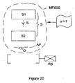
図19は、MFISISの第9の実施の形態の第1の変形を示すブロック図である。この実施の形態では、MFISISは、レチクルの頂部RTに開口部Oを備えるかまたはクロムで被膜された(CC)レチクルRを含む。光源の角度の大きさが入射瞳の角度の大きさより大きく設定されている診断照射状態に光源Sが設定される。これは、旗の形をした箱の中のコマンド”σ>1”として示される。製品(チップ)がこのクラスの照射状態では作動していないので、これは診断設定と呼ばれる。 FIG. 19 is a block diagram showing a first modification of the ninth embodiment of MFISIS. In this embodiment, the MFISIS includes a (CC) reticle R with an opening O at the top RT of the reticle or coated with chrome. The light source S is set in a diagnostic irradiation state in which the angle of the light source is set larger than the angle of the entrance pupil. This is shown as the command “σ> 1” in a flag-shaped box. Since the product (chip) is not working in this class of illumination, this is called a diagnostic setting.
図20はMFISISの第9の実施の形態の第2の変形を示し、この変形では、絞りプレートAPが、光源とレチクルステージRSとの間の離散位置に配置される。APは開口部Oを含む。光源Sは、再び旗の形の箱で示される診断設定”σ>1”で作動する。これは反射システムの有用な構成であり、この構成では、唯一加わったのが、レチクルステージRSに配置されたブランクで均一な反射(明視野の)レチクルである。 FIG. 20 shows a second modification of the ninth embodiment of the MFISIS, in which the aperture plate AP is arranged at discrete positions between the light source and the reticle stage RS. AP includes an opening O. The light source S operates again with a diagnostic setting “σ> 1” indicated by a flag-shaped box. This is a useful configuration of the reflective system, in which the only addition is a blank, uniform reflective (bright field) reticle placed on the reticle stage RS.
図21は、MFISISの第9の実施の形態の第3の変形を示すブロック図である。開口部Oを含む絞りプレートAPが、レチクルステージRSと、イメージング対物レンズIMO1の第1の部分との間に配置される。光源Sは“σ>1”の診断モードで作動する。唯一加わったのがレチクルステージRSに配置されたブランクで均一な反射(明視野の)レチクルである反射システムに、この構成が使用できる。これを達成する1つの方法は、露光の過程における角度で、または異なる角度での一連のサブ露光として、小さな(σ<1)光源を機械的にスキャンまたは傾かせる。
第10の実施の形態
FIG. 21 is a block diagram showing a third modification of the ninth embodiment of MFISIS. An aperture plate AP including an opening O is disposed between the reticle stage RS and the first portion of the imaging objective lens IMO1. The light source S operates in a diagnostic mode “σ> 1”. This configuration can be used in a reflective system where the only addition is a blank, uniform reflective (bright field) reticle placed on the reticle stage RS. One way to achieve this is to mechanically scan or tilt a small (σ <1) light source at an angle in the course of exposure or as a series of sub-exposures at different angles.
Tenth embodiment
図22は、第10の実施の形態のISISに関する断面を示す概略図である。図22に示されているように、ボールレンズBLはレチクルおもて面RFの下に位置し、絞りプレートAPのおおよそ開口部Oの上に焦点が合う。この配置の効果は、絞りプレートの離れた距離(zap)に比較して、ボールレンズBLの短い焦点距離のために、光源を多く捕まえることである。以下の構造パラメータを使用する1つの例は、
波長 =128nm
ボールレンズの直径 =1mm
ボールレンズの材料 =UVグレード石英ガラス
絞りプレートのピンホールの直径(Oの直径) =0.155mm
zap =4.923mm
絞りプレートからのボールレンズの離れた距離(図22のBLSO)=0.192mm
レチクルの側面の開口数(NA)>0.1の光源を捕らえる(すなわち、透過率=1をもつ固定角空間内の領域)。これは、より小さいNAをもつ光源は、このISISにより完全に通過して、マシンの射出瞳の均一で明るい照射となる。この装置の解像度は、NAres〜0.063のウェハー側面上の開口数に対応する。
FIG. 22 is a schematic diagram showing a cross section relating to the ISIS of the tenth embodiment. As shown in FIG. 22, the ball lens BL is positioned below the reticle front surface RF, and is focused on approximately the opening O of the aperture plate AP. The effect of this arrangement is to capture more light sources due to the short focal length of the ball lens BL compared to the distance (zap) of the aperture plate. One example using the following structure parameters is
Wavelength = 128nm
Ball lens diameter = 1 mm
Ball lens material = Pinhole diameter of UV grade quartz glass diaphragm plate (O diameter) = 0.155 mm
zap = 4.923 mm
The distance of the ball lens from the aperture plate (BLSO in FIG. 22) = 0.192 mm
Capture a light source with a numerical aperture (NA)> 0.1 on the side of the reticle (ie, a region in a fixed angle space with transmittance = 1). This is because a light source with a smaller NA passes completely through this ISIS, resulting in a uniform and bright illumination of the machine's exit pupil. The resolution of this device corresponds to a numerical aperture on the wafer side of NARes to 0.063.
電子センサとの使用に関して、この大きい明るさにより、ノイズと露光時間の減少とに役立つけれども、フォトレジストの被膜されたウェハーが記録媒体として利用されると、多くの手段の1つを用いることによりISISの透過率を減少させることができる。1つのメカニズムは、部分的に反射するかまたは部分的に吸収する被膜(減衰率約90から98%以上)で、レチクルの裏面RBを被膜することを含む。もう1つのメカニズムは、レチクルおもて面RF上の減衰位相シフトマスク材料(約6%の透過率)を利用することを含む。 For use with electronic sensors, this large brightness helps reduce noise and exposure time, but when a photoresist-coated wafer is utilized as a recording medium, it can be used by using one of many means. The transmittance of ISIS can be reduced. One mechanism involves coating the backside RB of the reticle with a partially reflective or partially absorbing coating (attenuation of about 90 to 98% or more). Another mechanism involves utilizing an attenuated phase shift mask material (approximately 6% transmission) on the reticle front surface RF.
解像度を増やすために(上記のNAresを減らすために)、単純に直径Oを短くするけれども、これにより、光源を捕らえるのが小さくなる。これはより小さなコヒーレンスまたはシグマ値で光源Sを作動させることによるか(これによりNAを減少させる)、または、レチクルおもて面RFまたはレチクル裏面RB上の格子構造を含むことにより(上記参照)、補うことができる。
第11の実施の形態
In order to increase the resolution (to reduce the above NAres), the diameter O is simply shortened, but this makes it less likely to capture the light source. This is due to operating the light source S with a smaller coherence or sigma value (thus reducing the NA) or by including a grating structure on the reticle front surface RF or reticle back surface RB (see above). Can make up.
Eleventh embodiment
図23は、第11の実施の形態のISISに関する断面を示す概略図である。この実施の形態では、ボールレンズBLが、レチクルの裏面RBより上に位置し、絞りプレートの(RB上でもある)開口部Oにほぼ焦点が合う。絞りプレートの離れた距離(zap)は、RFからAPの距離である。1つの例は以下の構造パラメータを使用する。
波長 =248nm
ボールレンズの直径 =1.8mm
ボールレンズの材料 =UVグレード石英ガラス
絞りプレートのピンホールの直径(Oの直径) =0.155mm
zap =4.923mm
絞りプレートからのボールレンズの離れた距離(図23のBLSO)=0.400mm
FIG. 23 is a schematic diagram showing a cross section relating to the ISIS of the eleventh embodiment. In this embodiment, the ball lens BL is positioned above the back surface RB of the reticle, and is substantially focused on the opening O (also on the RB) of the aperture plate. The distance (zap) of the diaphragm plate is the distance from RF to AP. One example uses the following structural parameters:
Wavelength = 248nm
Ball lens diameter = 1.8mm
Ball lens material = Pinhole diameter of UV grade quartz glass diaphragm plate (O diameter) = 0.155 mm
zap = 4.923 mm
The distance of the ball lens from the aperture plate (BLSO in FIG. 23) = 0.400 mm
再び電子センサの使用に関して、明るさが大きいと、ノイズおよび露光時間の減少に役立つけれども、フォトレジストの被膜されたウェハーが、記録媒体として使用されると、図22に関して説明したように、ISISの透過率を減少させることができる。 Again with respect to the use of the electronic sensor, a high brightness helps reduce noise and exposure time, but when a photoresist-coated wafer is used as the recording medium, as described with respect to FIG. The transmittance can be reduced.
再び、解像度を増やすために、Oの直径を短くすることは、光源を捕らえる率を低くする。図22に関連して説明したように、再び、これは、より小さなコヒーレンスまたはシグマ値で(これは開口数を減らす)光源Sを作動させることにより、または、レチクルのおもて面RFまたはレチクルの裏面RB上に格子構造を含むことにより補うことができる。 Again, to increase the resolution, reducing the diameter of O reduces the rate at which the light source is captured. Again, as explained in connection with FIG. 22, this can be done by activating the light source S with a smaller coherence or sigma value (which reduces the numerical aperture) or on the front face RF or reticle of the reticle. This can be compensated by including a lattice structure on the back surface RB of the substrate.
図22および図23に示された例では、ボールレンズが使用されていた。任意の他のタイプのレンズが使用できるのは当然である。同様に、図22および図23はレチクルを示し、格子を使用してもよいことは当然である。
追加の実施の形態
In the example shown in FIGS. 22 and 23, a ball lens is used. Of course, any other type of lens can be used. Similarly, FIGS. 22 and 23 show a reticle, and it should be understood that a grating may be used.
Additional embodiments
高NAリソグラフィ、好ましい実施の形態の方法は、有効開口数>1(液浸または他のリソグラフィ)で作動するリソグラフィシステムで使用できる。そのような場合に関して、組み合わせ材料およびレチクル側の方向余弦の屈折の指数によりウェハー側面上の方向余弦を調整することにより、透過率関数(方程式1)を補正する必要がある。例えば、浸液として水を使用すると、
![]()
ここで、
![]()
![]()
here,
![]()
したがって、以下で示す適切な記録媒体を使用して、液浸媒体のエネルギー分布を観察する必要があるかもしれない。方程式2が任意の媒体の一般的関係を示すことに注意する。
T(nx,ny)を計測する方法、第1の実施の形態
Therefore, it may be necessary to observe the energy distribution of the immersion medium using the appropriate recording medium shown below. Note that
Method for measuring T (nx, ny), first embodiment
図24は、適切な記録媒体で被膜されたシリコンウェハーを使用して射出瞳の透過率を計算する実施の形態を示す流れ図である。例えば、ウェハー上のフォトレジストに光源のイメージを記録するとき、図24のフローが使用できる。フローは、ここで説明するようにMFISISが設けられてマシン上に装填されたブロック2402から開始する。レジスト被膜された基板(ウェハー)が設けられ、マシン上に装填されたブロック2404にフローが続く。次にブロック2406において、基板は、ウェハー(または追加のウェハー)上の離散的に分離したイメージフィールドにおいて、複数回、増加する露光量で露光される。例えば、A.J.de Ruyter等による、“Examples of Illumination Source Effects on Imaging Performance”,ARCH Chemicals Microlithography Symposium,pp.1−8,2003の3ページを参照。フローはブロック2408に続き、次に基板が現像される。次にブロック2410では、露光されたイメージが1つずつ(照射ごとに)撮影(各フィールドポイントに関して複数の撮影)される。これらのイメージおよび露光シーケンスの知識から、 “加工していない”光強度の境界
![]()
![]()
![]()
![]()
この結果の対数は、ゼルニケ多項式関数に展開できる(図25)。さらに方程式11の結果を畳み込み積分の逆演算をして、可能なピンホールの平均化の結果を取り出す。
T(nx,ny)の計測方法、第2の実施の形態
The logarithm of this result can be expanded to a Zernike polynomial function (FIG. 25). Further, the result of
Measuring method of T (nx, ny), second embodiment
図26は、電子センサを使用して射出瞳の透過率を計測する実施の形態を示す流れ図である。例えば、フォトレジストの代わりに、イメージが電子的に記録(例えばCCDアレイ上に)されると、図26に要点の示されたステップが続く。図24に示されているこの方法と前の方法との間の違いは、記録されたセンサの出力が、直接 “加工していない”強度または光強度に関する信号を提供することである。必要ならば、ゲインのオフセットまたは適切なマッピングが“加工していない”強度信号を補正するために使用でき、最終的な正規化された光強度になる(方程式10)。加えて、同様なドライNA(NAウェット=NAドライ)における液浸システムの動作に関して、電子記録装置の焦点の深さ要件も考慮される。次に、ピンホール効果の畳み込み積分の逆演算は、第1の実施の形態でのように進行する。 FIG. 26 is a flowchart showing an embodiment in which the transmittance of an exit pupil is measured using an electronic sensor. For example, instead of photoresist, when the image is recorded electronically (eg on a CCD array), the steps outlined in FIG. 26 follow. The difference between this method shown in FIG. 24 and the previous method is that the recorded sensor output provides a signal that is directly “unprocessed” intensity or light intensity. If necessary, a gain offset or appropriate mapping can be used to correct the “unprocessed” intensity signal, resulting in the final normalized light intensity (Equation 10). In addition, with respect to the operation of the immersion system in similar dry NA (NA wet = NA dry), the depth of focus requirement of the electronic recording device is also taken into account. Next, the inverse operation of the convolution integral of the pinhole effect proceeds as in the first embodiment.
MFISISが設けられているブロック2602からフローが開始する。フローはブロック2604に続き、MFISISがマシン上に装着される。次にブロック2606で、電子センシングアレイが1回以上の照射で露光される。次に、ブロック2608に続き、
![]()
通信エラーの改善方法
The flow begins at
![]()
How to improve communication errors
次に、好ましい実施の形態に関する計測装置および計測方法により決定されるように、透過率関数T(nx,ny,x,y)を使用したリソグラフィ露光ツールに一意に関連する通信に関するエラーを改善するいくつかの方法を説明する。
開口数誤差調整
Next, improve communication errors uniquely associated with the lithography exposure tool using the transmission function T (nx, ny, x, y) as determined by the metrology apparatus and metrology method for the preferred embodiment. Several methods are described.
Numerical error adjustment
第1に、各フィールドポイント(i)に関し、シータの関数(瞳の角度の大きさ)として最大半角のsinを決定することにより、有効なT(nx,ny)iマップから開口数(NAi)を抽出する。次に、これは各フィールドポイントに関して有効NAをもたらす。次に、フィールドポイント(N)の全体の数またはNAavg=ΣNAi/Nにわたって単純に加算することにより、システムの平均NA(NAavg)を計算する。名目上または所望のNA設定からこれが異なる程度まで、適切な開口絞り(AS、図1)における物理的羽根が、所望の設定に調整できる。
開口数誤差調整(楕円形のシステム)
First, for each field point (i), the numerical aperture (NA i ) is determined from the effective T (nx, ny) i map by determining the maximum half-width sin as a theta function (the pupil angle magnitude). ). This then yields a valid NA for each field point. Next, the average NA (NAavg) of the system is calculated by simply adding over the total number of field points (N) or NAavg = ΣNA i / N. From the nominal or desired NA setting to the extent that this differs, the physical vanes at the appropriate aperture stop (AS, FIG. 1) can be adjusted to the desired setting.
Numerical error adjustment (elliptical system)
楕円形に調整できるフォトリソグラフィ露光システム(楕円NAシステム)の射出瞳開口数誤差の改善方法は、以下のステップを含む。ステップ1、フィールド位置の関数としてT(nx,ny)を決定する本発明の方法を使用して、各コンポーネントに関する平均化方法を使用して、各フィールドポイントに関するNA(NAx,NAy)のxおよびyコンポーネントを決定するステップ。ステップ2、ΔNA=MAX|NAx−NAy|を使用して計測(または補間)された全てのフィールドポイントに関し、NAの中の最大離心率を決定するステップ。ステップ3、ΔNA>方法の許容差(シミュレーションにより判明または決定される)であると、マシンを調整して問題を修正する(例えば、楕円のNAシステムパラメータを調整する)ステップを含む。
A method for improving the exit pupil numerical aperture error of a photolithographic exposure system (elliptical NA system) that can be adjusted to an elliptical shape includes the following steps.
ピントのずれを補正する方法は以下のステップを含む。ステップ1、以下の方程式および既知の透過率関数を使用して平均誤差を計算するステップ。
![]()
![]()
サンプリング
The method for correcting the focus shift includes the following steps.
![]()
![]()
sampling
レンズ透過率が時間の経過により変化する(上記の“Impact of Across Pupil Transmittance Variation in Projection Lenses on Fine Device Pattern Imaging“を参照)ことを期待するので、インサイチュウ透過率計測は適切な時間間隔で行われ、時間の関数がルートの同定を助けるために使用できるので、ログを取るか記録する透過率マップは適切な改善スケジュールを提供する。
グレイレベル補正
Since the lens transmittance is expected to change over time (see “Impact of Across Pulp Transmission Variation in Projection Lens Device Pattern Imaging” above, the in-situ time transmittance measurement is an appropriate in-situ time interval measurement) Since a function of time can be used to help identify the route, a logging map that logs or records provides an appropriate improvement schedule.
Gray level correction
露光フィールドにわたる透過率誤差の改善方法は以下のステップを含む。ステップ1、好ましい実施の形態に説明されているように、フォトリソグラフィ露光システムの透過率特性を決定するステップ。ステップ2、方向余弦の関数としての各フィールドポイントの透過率の平均値Tavg(n)=ΣT(n)i/Nを計算するステップ。ステップ3、アクセスできる瞳を備えた上記のフォトリソグラフィシステムに関し、グレイレベル瞳フィルタを構成して、瞳平面の高レベルの透過率を平均するステップを含む。注:Tavg(n)<1であって、フィルタは空間的に調整されて、高強度の領域を正規化されたノイズ強度に下げる。
主な実施の形態の変形
The method for improving the transmission error over the exposure field includes the following steps.
Variations of the main embodiment
上記の実施の形態の多くの変形が可能である。 Many variations of the above embodiment are possible.
全てのMFISISの設計の内で、当業者に知られるように、(その設計値に関して)知られている程度までは補うことができるために、イメージの歪みは重要な設計上の制約ではない。
偏光
Within all MFISIS designs, image distortion is not an important design constraint because it can be compensated to a known degree (with respect to its design value) as known to those skilled in the art.
Polarization
好ましい実施の形態の装置および方法は、非偏光光源または調整できる偏光をもつ光源を使用して、偏光に対する透過感度を計測するように構成できる。非偏光光源の場合には、偏光された光(適切なジョーンズベクトルにより与えられる)をウェハー平面に当てるように、照射レンズまたはレチクル(好ましい実施の形態に関して)は調整できる(可能ならば組み合わせて)。照射システムの変更は、偏光器、フィルタ、および可能ならば基準以下の解像度の格子の組合せを含む(E.Hecht,“Optics”,Addison Wesley,第2版,1987,pp279,497を参照)。好ましい実施の形態に関するレチクルの変更は、以下の表面または材料、平凸レンズの頂部または底部、レチクルの頂部または底部、レチクルの頂部または底部、ピンホールの開口部、のいずれか1つに関するISIS構造に基準以下の解像度の格子を加えるステップ(2つの可能な構成は図27および図28に示されている)を含む。加えて、偏光フィルタが使用できて、同様な方法で追加されるか、またはピンホールの形状が、所望の偏光状態に垂直な方向をもつスリットの形をとることができる。加えて、図4、図11、図12、図14、図15、および図16に示されているISIS構造の変形は、構成設計および偏光に関する同じ技術を使用しても可能である。調整できる偏光をもつ光源に関して、レチクルは上に説明したように調整できるけれども、照射レンズが偏光を変更できるので、計測は、ISIS構造に当たる光の偏光状態を決定するために行われるべきである。このように、ISIS構造はそのような変更を調整できる。得られた情報は、主に、異なる偏光状態に関して、透過率の違いが、偏光により引き起こされたコントラストの損失(ウェハー表面における方向余弦の関数)を研究(シミュレート)するために使用できる。
レチクル側面のテレセントリック性
The apparatus and method of the preferred embodiment can be configured to measure transmission sensitivity to polarized light using a non-polarized light source or a light source with adjustable polarization. In the case of a non-polarized light source, the illumination lens or reticle (with respect to the preferred embodiment) can be adjusted (combined if possible) to direct polarized light (given by the appropriate Jones vector) to the wafer plane. . Modifications to the illumination system include a combination of polarizers, filters, and possibly sub-standard resolution gratings (see E. Hecht, “Optics”, Addison Wesley, 2nd edition, 1987, pp 279, 497). The reticle modifications for the preferred embodiment are in the ISIS structure for any one of the following surfaces or materials, the top or bottom of the plano-convex lens, the top or bottom of the reticle, the top or bottom of the reticle, or the opening of the pinhole. Adding a sub-standard resolution grid (two possible configurations are shown in FIGS. 27 and 28). In addition, polarizing filters can be used and added in a similar manner, or the pinhole shape can take the form of a slit with a direction perpendicular to the desired polarization state. In addition, variations of the ISIS structure shown in FIGS. 4, 11, 12, 14, 15, and 16 are possible using the same techniques for configuration design and polarization. For light sources with adjustable polarization, the reticle can be adjusted as described above, but since the illumination lens can change the polarization, measurements should be made to determine the polarization state of the light impinging on the ISIS structure. In this way, the ISIS structure can accommodate such changes. The obtained information can be used mainly to study (simulate) the loss of contrast (a function of the direction cosine at the wafer surface) caused by the polarization difference for different polarization states.
Telecentricity of the reticle side
フィールド位置の関数として、レチクル側面のテレセントリック性(RSTC)を決定する装置および方法は、図29に示されている。図29は、フィールド位置の関数として、レチクル側面のテレセントリック性(RSTC)を決定する実施の形態を示す流れ図である。フローは、MFISISおよび参照フレームが設けられているブロック2902から開始する。次に、ブロック2904でMFISISがマシン上に装着される。次に、ブロック2906において、露光照射量が1以上のウェハー上を蛇行する。次に、ブロック2908では、ウェハーが現像される。ブロック2910では、変化する照射量における射出瞳の現像されたイメージが撮像される。フローはブロック2912に続き、
![]()
![]()
次にブロック2914において、この方法は、イメージフレームの中央と、射出瞳の中央(レジストに印刷されるように)の距離を、フィールド位置の関数として計測するステップ、
Claims (65)
光入力部;および
上記光調節器が、上記光入力部において、光源から光を受け、上記投射イメージングシステムの入射瞳の角度の大きさより大きい角度をもつ実質的に均一な照射光を出力する光出力部
を備える光調節器。 A light modulator of a projection imaging system,
A light input unit; and light that receives light from a light source at the light input unit and outputs substantially uniform irradiation light having an angle larger than an incident pupil angle of the projection imaging system. Light regulator with output.
第1の表面および第2の表面を備えるレチクル;
上記レチクルの上記第1の表面に隣接した少なくとも1枚のレンズ
被膜の開口部が上記少なくとも1枚のレンズの1つに対応する上記被膜の少なくとも1つの開口部を備えた上記レチクルの上記第2の表面上の被膜
をさらに備える光調節器。 The light regulator according to claim 1,
A reticle comprising a first surface and a second surface;
The second of the reticle, wherein the opening of at least one lens coating adjacent to the first surface of the reticle comprises at least one opening of the coating corresponding to one of the at least one lens. A light regulator further comprising a coating on the surface of the surface.
第1の表面上に少なくとも1つの開口部を有し、第2の表面上に対応する光開口部を有する上記第1の表面および上記第2の表面を備えたレチクル;
上記レチクルの上記第1の表面上の上記光開口部に隣接し、頂部表面および底部表面を備えた少なくとも1枚のレンズ;および
絞りプレートの開口部が上記第2の表面上の光開口部に対応し、上記少なくとも1枚のレンズの頂部に受けた光が、投射イメージングシステムの入射瞳の角度の大きさより大きい角度の大きさをもつ実質的に均一な照射光として、上記レチクルを通過し、上記絞りプレートの少なくとも1つの開口部を通って出力される少なくとも1つの開口部をもつ絞りプレート
を備える光調節器。 A light regulator,
A reticle comprising the first surface and the second surface having at least one opening on the first surface and a corresponding light opening on the second surface;
At least one lens adjacent to the optical aperture on the first surface of the reticle and having a top surface and a bottom surface; and an aperture in the aperture plate is an optical aperture on the second surface Correspondingly, the light received at the top of the at least one lens passes through the reticle as substantially uniform illumination with an angular magnitude greater than the angular magnitude of the entrance pupil of the projection imaging system; A light controller comprising: an aperture plate having at least one aperture that is output through at least one aperture of the aperture plate.
レチクル;
バルク拡散器;および
上記レチクルおよび上記バルク拡散器を通過する光が、投射イメージングシステムの入射瞳の角度の大きさよりも大きい角度の大きさをもつ実質的に均一な照射光として、絞りプレートの少なくとも1つの開口部を通って出力される少なくとも1つの開口部をもつ絞りプレート
を備える光調節器。 A light regulator,
Reticle;
A bulk diffuser; and light passing through the reticle and the bulk diffuser as substantially uniform illumination with an angular magnitude greater than the angular magnitude of the entrance pupil angle of the projection imaging system; A light regulator comprising an aperture plate having at least one opening that is output through one opening.
第1の表面上に少なくとも1つの光開口部を有し、第2の表面上に対応する光開口部を有する上記第1の表面および上記第2の表面を備えたレチクル;
第1のレンズおよび第2のレンズが上記レチクルの光開口部に連結され、隣接する上記レチクルの上記第1の表面に隣接した少なくとも1つの上記第1のレンズおよび上記レチクルの上記第2の表面に隣接した第2のレンズ;および
絞りプレートの開口部が、上記レチクルの上記第2の表面上の光開口部に対応し、上記第1のレンズの頂部で受けた光が上記レチクルと第2のレンズとを通過し、投射イメージングシステムの射出瞳の角度の大きさより大きい角度の大きさをもつ実質的に均一な照射光として、上記絞りプレートの少なくとも1つの開口部を通って出力される少なくとも1つの開口部を備えた絞りプレート
を備える光調節器。 A light regulator,
A reticle having the first surface and the second surface having at least one light opening on the first surface and a corresponding light opening on the second surface;
A first lens and a second lens are coupled to the optical aperture of the reticle, and at least one of the first lens and the second surface of the reticle adjacent to the first surface of the adjacent reticle. A second lens adjacent to the aperture; and an aperture of the aperture plate corresponds to a light aperture on the second surface of the reticle, and light received at the top of the first lens is coupled to the reticle and the second At least as output through the at least one aperture of the diaphragm plate as substantially uniform illumination light having an angle magnitude greater than the magnitude of the exit pupil angle of the projection imaging system. A light conditioner comprising an aperture plate with one opening.
第1のレンズを含む第1の反射表面;
第2のレンズを含む第2の反射表面;および
絞りプレートの開口部が上記第1のレンズおよび上記第2のレンズと連結され、上記第1のレンズに入射する光が上記第2のレンズに反射され、上記第2のレンズに反射された後、投射イメージングシステムの入射瞳の角度の大きさより大きい角度の大きさをもつ実質的に均一な照射光として上記絞りプレートの開口部を通過する開口部を備えた絞りプレート
を備える光調節器。 A light regulator,
A first reflective surface comprising a first lens;
A second reflective surface including a second lens; and an aperture of the aperture plate coupled to the first lens and the second lens, so that light incident on the first lens is incident on the second lens An aperture that is reflected and reflected by the second lens and then passes through the aperture of the aperture plate as substantially uniform illumination with an angle magnitude greater than the magnitude of the entrance pupil angle of the projection imaging system. A light regulator comprising an aperture plate having a section.
光源、レチクルステージ、入射瞳、射出瞳、およびイメージング対物レンズを含むリソグラフィ投射マシン;
上記リソグラフィ投射マシンの上記光源を調節して、上記入射瞳をいっぱいにする手段;
絞りプレート
を備える光調節器。 A light regulator,
A lithographic projection machine comprising a light source, a reticle stage, an entrance pupil, an exit pupil, and an imaging objective;
Means for adjusting the light source of the lithographic projection machine to fill the entrance pupil;
Light controller with an aperture plate.
頂部表面および底部表面をもつレチクル;
レンズ、および上記レンズを上記レチクルに取り付ける手段;および
絞りプレートおよび上記絞りプレートを上記レチクルに取り付ける手段
を備える光調節器。 A light regulator,
A reticle having a top surface and a bottom surface;
A light adjuster comprising: a lens; and means for attaching the lens to the reticle; and means for attaching the aperture plate and the aperture plate to the reticle.
上記投射イメージングシステムの入射瞳の角度の大きさより大きい角度をもつ実質的に均一な照射光をもつ照射源を設けるステップ;
上記照射イメージングシステムの射出瞳から発せられる照射光源からの照射光により記録媒体を露光するステップ;および
上記露光された記録媒体から、上記投射イメージングシステムの透過率関数を再構成するステップ
を含む方法。 A method for determining exit pupil transmittance of a projection imaging system, comprising:
Providing an illumination source with substantially uniform illumination light having an angle greater than the magnitude of the entrance pupil angle of the projection imaging system;
Exposing a recording medium with illumination light from an illumination light source emanating from an exit pupil of the illumination imaging system; and reconstructing a transmission function of the projection imaging system from the exposed recording medium.
上記投射イメージングシステムの入射瞳の角度の大きさより大きい角度をもつ実質的に均一な照射光を備えた照射光源を設けるステップ;
上記投射イメージングシステムの射出瞳から発せられる上記照射光源からの照射光で記録媒体を露光するステップ;
露光された上記記録媒体からフィールド位置の関数として上記投射イメージングシステムの透過率関数を再構成するステップ;
基準フレームの中央と各フィールドポイントの上記露光された射出瞳の中央との間の違いを決定するステップ;および
レチクル側面のテレセントリック性の個々のコンポーネントを計算するステップ
を含む方法。 A method for determining telecentricity of a reticle side of a projection imaging system, comprising:
Providing an illumination light source with a substantially uniform illumination light having an angle greater than the magnitude of the angle of the entrance pupil of the projection imaging system;
Exposing the recording medium with irradiation light from the irradiation light source emitted from an exit pupil of the projection imaging system;
Reconstructing the transmission function of the projection imaging system as a function of field position from the exposed recording medium;
Determining the difference between the center of the reference frame and the center of the exposed exit pupil of each field point; and calculating the individual components of reticle side telecentricity.
投射イメージングシステムの入射瞳の角度の大きさよりも大きい角度の大きさの実質的に均一な照射光をもつ照射光源を設けるステップ;
上記投射イメージングシステムの射出瞳から発せられる照射光源からの照射光で記録媒体を露光するステップ;
露光された上記記録媒体から上記投射イメージングシステムの透過率関数を再構成するステップ;
再構成された上記透過率プロファイルにしたがって上記投射イメージングシステムの絞りを調節するステップ;および
上記投射イメージングシステムの所望のマスク・ワーク・レチクルを投射するステップ
を含む方法。 A method of manufacturing a photolithographic chip mask, comprising:
Providing an illuminating light source having a substantially uniform illuminating light with an angular magnitude greater than the angular magnitude of the entrance pupil of the projection imaging system;
Exposing the recording medium with irradiation light from an irradiation light source emitted from an exit pupil of the projection imaging system;
Reconstructing the transmission function of the projection imaging system from the exposed recording medium;
Adjusting the aperture of the projection imaging system according to the reconstructed transmission profile; and projecting a desired mask work reticle of the projection imaging system.
投射イメージングシステムの入射瞳の角度の大きさより大きい角度の大きさの実質的に均一な照射光をもつ照射光源を設けるステップ;
上記投射イメージングシステムの射出瞳から発せられる照射光源からの照射光で記録媒体を露光するステップ;
露光された上記記録媒体から、上記投射イメージングシステムの透過率関数を再構成するステップ;
再構成された上記透過率プロファイルにしたがって上記投射イメージングシステムの絞りを調節するステップ;および
上記投射イメージングシステムの所望のマスク・ワーク・レチクルを投射するステップ
を含む方法。 A method for manufacturing a semiconductor chip, comprising:
Providing an illumination light source having a substantially uniform illumination light with an angle magnitude greater than the angle magnitude of the entrance pupil angle of the projection imaging system;
Exposing the recording medium with irradiation light from an irradiation light source emitted from an exit pupil of the projection imaging system;
Reconstructing the transmission function of the projection imaging system from the exposed recording medium;
Adjusting the aperture of the projection imaging system according to the reconstructed transmission profile; and projecting a desired mask work reticle of the projection imaging system.
投射イメージングシステムの入射瞳の角度の大きさより大きい角度の大きさの実質的に均一な照射光をもつ照射光源を設けるステップ;
上記投射イメージングシステムの射出瞳から発せられる上記照射光源からの照射光で、記録媒体を露光するステップ;
露光された上記記録媒体から上記投射イメージングシステムの透過率関数を再構成するステップ;および
再構成された上記透過率プロファイルにしたがって、上記投射イメージングシステムの絞りの調節を制御するステップ;
を含む方法。 A method for controlling a projection imaging system comprising:
Providing an illumination light source having a substantially uniform illumination light with an angle magnitude greater than the angle magnitude of the entrance pupil angle of the projection imaging system;
Exposing the recording medium with irradiation light from the irradiation light source emitted from an exit pupil of the projection imaging system;
Reconstructing the transmission function of the projection imaging system from the exposed recording medium; and controlling the adjustment of the aperture of the projection imaging system according to the reconstructed transmission profile;
Including methods.
Applications Claiming Priority (2)
| Application Number | Priority Date | Filing Date | Title |
|---|---|---|---|
| US56263204P | 2004-04-14 | 2004-04-14 | |
| PCT/US2005/012519 WO2005106593A2 (en) | 2004-04-14 | 2005-04-13 | Method and apparatus for measurement of exit pupil transmittance |
Publications (1)
| Publication Number | Publication Date |
|---|---|
| JP2007534166A true JP2007534166A (en) | 2007-11-22 |
Family
ID=34965809
Family Applications (1)
| Application Number | Title | Priority Date | Filing Date |
|---|---|---|---|
| JP2007508495A Pending JP2007534166A (en) | 2004-04-14 | 2005-04-13 | Method and apparatus for measuring exit pupil transmittance |
Country Status (3)
| Country | Link |
|---|---|
| US (2) | US7688426B2 (en) |
| JP (1) | JP2007534166A (en) |
| WO (1) | WO2005106593A2 (en) |
Families Citing this family (10)
| Publication number | Priority date | Publication date | Assignee | Title |
|---|---|---|---|---|
| US7259827B2 (en) * | 2004-07-14 | 2007-08-21 | Asml Netherlands B.V. | Diffuser unit, lithographic apparatus, method for homogenizing a beam of radiation, a device manufacturing method and device manufactured thereby |
| JP2008527756A (en) * | 2005-01-19 | 2008-07-24 | ライテル・インストルメンツ | Method and apparatus for measuring light source coherence matrix |
| US20090115986A1 (en) * | 2005-06-02 | 2009-05-07 | Carl Zeiss Smt Ag | Microlithography projection objective |
| US7846624B2 (en) | 2006-02-17 | 2010-12-07 | Litel Instruments | Systems and methods for determination of focus and telecentricity, amelioration of metrology induced effects and application to determination of precision bossung curves |
| US8033471B2 (en) * | 2008-05-08 | 2011-10-11 | Psion Teklogix Inc. | Optical image reader |
| US7952799B2 (en) * | 2009-06-19 | 2011-05-31 | Corning Incorporated | Extreme broadband compact optical system with multiple fields of view |
| NL2007367A (en) * | 2010-11-01 | 2012-05-02 | Asml Netherlands Bv | Lithographic apparatus and method. |
| US10133184B2 (en) | 2012-04-25 | 2018-11-20 | Nikon Corporation | Using customized lens pupil optimization to enhance lithographic imaging in a source-mask optimization scheme |
| US9030668B2 (en) * | 2012-05-15 | 2015-05-12 | Nikon Corporation | Method for spatially multiplexing two or more fringe projection signals on a single detector |
| CN118896565B (en) * | 2024-10-09 | 2024-12-03 | 中国航发贵州黎阳航空动力有限公司 | Device and method for detecting punching angle by utilizing light transmission gap |
Citations (25)
| Publication number | Priority date | Publication date | Assignee | Title |
|---|---|---|---|---|
| JPH0365623A (en) * | 1989-08-03 | 1991-03-20 | Hitachi Ltd | Projection exposure method and apparatus |
| JPH06267818A (en) * | 1993-03-11 | 1994-09-22 | Nikon Corp | Projection exposure device |
| JPH07220995A (en) * | 1994-01-31 | 1995-08-18 | Nec Corp | Light intensity distribution simulating method |
| US5978085A (en) * | 1997-03-07 | 1999-11-02 | Litel Instruments | Apparatus method of measurement and method of data analysis for correction of optical system |
| JP2000021732A (en) * | 1998-07-02 | 2000-01-21 | Toshiba Corp | Exposure equipment inspection method |
| JP2001500628A (en) * | 1996-02-28 | 2001-01-16 | ケニス シー ジョンソン | Microlens scanner for microlithography and wide field confocal microscope |
| JP2001230180A (en) * | 2000-02-15 | 2001-08-24 | Toshiba Corp | Exposure apparatus inspection method and exposure apparatus inspection photomask |
| JP2001230179A (en) * | 2000-02-15 | 2001-08-24 | Toshiba Corp | Inspection method for exposure equipment |
| JP2002022609A (en) * | 2000-07-10 | 2002-01-23 | Canon Inc | Projection exposure equipment |
| JP2002110540A (en) * | 2000-09-01 | 2002-04-12 | Asm Lithography Bv | Method of operating a lithographic apparatus, lithographic apparatus, device manufacturing method, and device manufactured thereby |
| JP2002139406A (en) * | 2000-11-06 | 2002-05-17 | Nikon Corp | Optical characteristic measuring mask, optical characteristic measuring method, and method of manufacturing exposure apparatus |
| JP2002169083A (en) * | 2000-11-30 | 2002-06-14 | Nikon Corp | Objective optical system, aberration measuring device, projection exposure device, method of manufacturing objective optical system, method of manufacturing aberration measuring device, method of manufacturing projection exposure device, and method of manufacturing micro device |
| JP2002174565A (en) * | 2000-12-06 | 2002-06-21 | Canon Inc | Aberration measurement device |
| JP2002329653A (en) * | 2001-04-27 | 2002-11-15 | Toshiba Corp | Method of measuring uneven illuminance of exposure apparatus, method of correcting uneven illuminance, method of manufacturing semiconductor device, and exposure apparatus |
| JP2003504861A (en) * | 1999-07-01 | 2003-02-04 | エイエスエムエル ネザランドズ ベスローテン フエンノートシャップ | Apparatus and method for image enhancement by spatial filtering |
| JP2003075990A (en) * | 2001-09-07 | 2003-03-12 | Toshiba Corp | Inspection mask and inspection method of exposure apparatus |
| JP2003156832A (en) * | 2001-11-22 | 2003-05-30 | Mitsubishi Electric Corp | Aberration measurement photomask, aberration measurement method, aberration measurement device and device manufacturing method |
| JP2003232901A (en) * | 2002-02-07 | 2003-08-22 | Canon Inc | Optical element, illumination device and exposure device |
| JP2003255512A (en) * | 2002-03-04 | 2003-09-10 | Fujitsu Ltd | Mask, effective optical path measuring method, and exposure apparatus |
| JP2004061515A (en) * | 2002-07-29 | 2004-02-26 | Cark Zeiss Smt Ag | Method and device for determining influence onto polarization state by optical system, and analyzer |
| JP2004095871A (en) * | 2002-08-30 | 2004-03-25 | Toshiba Corp | Exposure apparatus inspection method and exposure apparatus |
| JP2004297046A (en) * | 2003-03-07 | 2004-10-21 | Canon Inc | Aberration measurement method |
| JP2004363448A (en) * | 2003-06-06 | 2004-12-24 | Canon Inc | Exposure equipment |
| JP2005116733A (en) * | 2003-10-07 | 2005-04-28 | Toshiba Corp | Exposure apparatus inspection mask, exposure apparatus inspection method, and exposure apparatus |
| JP2007516612A (en) * | 2004-04-28 | 2007-06-21 | ライテル・インストルメンツ | Apparatus and method for determining dynamic lens field bending |
Family Cites Families (23)
| Publication number | Priority date | Publication date | Assignee | Title |
|---|---|---|---|---|
| US5136413A (en) | 1990-11-05 | 1992-08-04 | Litel Instruments | Imaging and illumination system with aspherization and aberration correction by phase steps |
| JP2816298B2 (en) * | 1992-10-09 | 1998-10-27 | 三菱電機株式会社 | Projection exposure apparatus and projection exposure method |
| US5392119A (en) | 1993-07-13 | 1995-02-21 | Litel Instruments | Plate correction of imaging systems |
| US5501925A (en) | 1994-05-27 | 1996-03-26 | Litel Instruments | High power masks and methods for manufacturing same |
| US5733708A (en) | 1995-10-02 | 1998-03-31 | Litel Instruments | Multilayer e-beam lithography on nonconducting substrates |
| JP3618450B2 (en) * | 1995-11-15 | 2005-02-09 | 株式会社ソキア | Multi-axis laser interferometer |
| US5640233A (en) | 1996-01-26 | 1997-06-17 | Litel Instruments | Plate correction technique for imaging systems |
| US5929991A (en) | 1997-03-07 | 1999-07-27 | Litel Instruments | Single plate corrector for stepper lens train |
| US5828455A (en) | 1997-03-07 | 1998-10-27 | Litel Instruments | Apparatus, method of measurement, and method of data analysis for correction of optical system |
| US6268904B1 (en) | 1997-04-23 | 2001-07-31 | Nikon Corporation | Optical exposure apparatus and photo-cleaning method |
| US6356345B1 (en) | 1998-02-11 | 2002-03-12 | Litel Instruments | In-situ source metrology instrument and method of use |
| US6157502A (en) * | 1998-07-02 | 2000-12-05 | Digital Optics Corporation | Optical bench circularizer having alignment indentations and associated methods |
| JP2000277415A (en) * | 1999-03-25 | 2000-10-06 | Canon Inc | Exposure equipment |
| JP2001168000A (en) * | 1999-12-03 | 2001-06-22 | Nikon Corp | Method of manufacturing exposure apparatus and method of manufacturing micro device using exposure apparatus manufactured by the method |
| US6704090B2 (en) * | 2000-05-11 | 2004-03-09 | Nikon Corporation | Exposure method and exposure apparatus |
| US6573986B2 (en) | 2000-12-08 | 2003-06-03 | Litel Instruments | Method and apparatus for self-referenced projection lens distortion mapping |
| KR100455684B1 (en) * | 2001-01-24 | 2004-11-06 | 가부시끼가이샤 도시바 | Focus monitoring method, exposure apparatus and mask for exposure |
| TWI220998B (en) * | 2001-02-13 | 2004-09-11 | Nikon Corp | Exposure method, exposure apparatus and manufacture method of the same |
| US6960415B2 (en) * | 2001-10-01 | 2005-11-01 | Canon Kabushiki Kaisha | Aberration measuring method and projection exposure apparatus |
| TWI277827B (en) * | 2003-01-14 | 2007-04-01 | Asml Masktools Bv | Method of optical proximity correction design for contact hole mask |
| US7046342B2 (en) * | 2004-01-29 | 2006-05-16 | International Business Machines Corporation | Apparatus for characterization of photoresist resolution, and method of use |
| US7079223B2 (en) * | 2004-02-20 | 2006-07-18 | International Business Machines Corporation | Fast model-based optical proximity correction |
| WO2006064593A1 (en) * | 2004-12-13 | 2006-06-22 | Harison Toshiba Lighting Corp. | Lighting equipment and lighting system |
-
2005
- 2005-04-13 JP JP2007508495A patent/JP2007534166A/en active Pending
- 2005-04-13 WO PCT/US2005/012519 patent/WO2005106593A2/en not_active Ceased
- 2005-04-13 US US11/105,799 patent/US7688426B2/en not_active Expired - Fee Related
-
2010
- 2010-02-09 US US12/703,100 patent/US8786827B2/en not_active Expired - Fee Related
Patent Citations (25)
| Publication number | Priority date | Publication date | Assignee | Title |
|---|---|---|---|---|
| JPH0365623A (en) * | 1989-08-03 | 1991-03-20 | Hitachi Ltd | Projection exposure method and apparatus |
| JPH06267818A (en) * | 1993-03-11 | 1994-09-22 | Nikon Corp | Projection exposure device |
| JPH07220995A (en) * | 1994-01-31 | 1995-08-18 | Nec Corp | Light intensity distribution simulating method |
| JP2001500628A (en) * | 1996-02-28 | 2001-01-16 | ケニス シー ジョンソン | Microlens scanner for microlithography and wide field confocal microscope |
| US5978085A (en) * | 1997-03-07 | 1999-11-02 | Litel Instruments | Apparatus method of measurement and method of data analysis for correction of optical system |
| JP2000021732A (en) * | 1998-07-02 | 2000-01-21 | Toshiba Corp | Exposure equipment inspection method |
| JP2003504861A (en) * | 1999-07-01 | 2003-02-04 | エイエスエムエル ネザランドズ ベスローテン フエンノートシャップ | Apparatus and method for image enhancement by spatial filtering |
| JP2001230180A (en) * | 2000-02-15 | 2001-08-24 | Toshiba Corp | Exposure apparatus inspection method and exposure apparatus inspection photomask |
| JP2001230179A (en) * | 2000-02-15 | 2001-08-24 | Toshiba Corp | Inspection method for exposure equipment |
| JP2002022609A (en) * | 2000-07-10 | 2002-01-23 | Canon Inc | Projection exposure equipment |
| JP2002110540A (en) * | 2000-09-01 | 2002-04-12 | Asm Lithography Bv | Method of operating a lithographic apparatus, lithographic apparatus, device manufacturing method, and device manufactured thereby |
| JP2002139406A (en) * | 2000-11-06 | 2002-05-17 | Nikon Corp | Optical characteristic measuring mask, optical characteristic measuring method, and method of manufacturing exposure apparatus |
| JP2002169083A (en) * | 2000-11-30 | 2002-06-14 | Nikon Corp | Objective optical system, aberration measuring device, projection exposure device, method of manufacturing objective optical system, method of manufacturing aberration measuring device, method of manufacturing projection exposure device, and method of manufacturing micro device |
| JP2002174565A (en) * | 2000-12-06 | 2002-06-21 | Canon Inc | Aberration measurement device |
| JP2002329653A (en) * | 2001-04-27 | 2002-11-15 | Toshiba Corp | Method of measuring uneven illuminance of exposure apparatus, method of correcting uneven illuminance, method of manufacturing semiconductor device, and exposure apparatus |
| JP2003075990A (en) * | 2001-09-07 | 2003-03-12 | Toshiba Corp | Inspection mask and inspection method of exposure apparatus |
| JP2003156832A (en) * | 2001-11-22 | 2003-05-30 | Mitsubishi Electric Corp | Aberration measurement photomask, aberration measurement method, aberration measurement device and device manufacturing method |
| JP2003232901A (en) * | 2002-02-07 | 2003-08-22 | Canon Inc | Optical element, illumination device and exposure device |
| JP2003255512A (en) * | 2002-03-04 | 2003-09-10 | Fujitsu Ltd | Mask, effective optical path measuring method, and exposure apparatus |
| JP2004061515A (en) * | 2002-07-29 | 2004-02-26 | Cark Zeiss Smt Ag | Method and device for determining influence onto polarization state by optical system, and analyzer |
| JP2004095871A (en) * | 2002-08-30 | 2004-03-25 | Toshiba Corp | Exposure apparatus inspection method and exposure apparatus |
| JP2004297046A (en) * | 2003-03-07 | 2004-10-21 | Canon Inc | Aberration measurement method |
| JP2004363448A (en) * | 2003-06-06 | 2004-12-24 | Canon Inc | Exposure equipment |
| JP2005116733A (en) * | 2003-10-07 | 2005-04-28 | Toshiba Corp | Exposure apparatus inspection mask, exposure apparatus inspection method, and exposure apparatus |
| JP2007516612A (en) * | 2004-04-28 | 2007-06-21 | ライテル・インストルメンツ | Apparatus and method for determining dynamic lens field bending |
Also Published As
| Publication number | Publication date |
|---|---|
| US8786827B2 (en) | 2014-07-22 |
| US20110007298A1 (en) | 2011-01-13 |
| US20050237512A1 (en) | 2005-10-27 |
| US7688426B2 (en) | 2010-03-30 |
| WO2005106593A2 (en) | 2005-11-10 |
| WO2005106593A3 (en) | 2006-04-13 |
Similar Documents
| Publication | Publication Date | Title |
|---|---|---|
| US8786827B2 (en) | Method and apparatus for measurement of exit pupil transmittance | |
| US7864296B2 (en) | Exposure apparatus, setting method, and exposure method having the same | |
| JP4343706B2 (en) | Reticle and optical property measurement method | |
| US10274370B2 (en) | Inspection apparatus and method | |
| JP4914408B2 (en) | Catadioptric optical system for light diffusion measurement | |
| JP4188370B2 (en) | Aberration measurement method and apparatus for reflective diffractive elements tuned for EUV lithography systems | |
| JP3950858B2 (en) | Wavefront measurement system, EUV photolithography system, and method for measuring wavefront of optical system | |
| JP3998627B2 (en) | Lithographic apparatus and measurement system | |
| US20080007705A1 (en) | In-Situ Interferometer Arrangement | |
| JP2002334831A (en) | Lithographic projection apparatus, diffraction module, sensor module and method for measuring wavefront aberration | |
| US6972836B2 (en) | Measuring method of illuminance unevenness of exposure apparatus, correcting method of illuminance unevenness, manufacturing method of semiconductor device, and exposure apparatus | |
| US7030998B2 (en) | Phase measurement apparatus for measuring characterization of optical thin films | |
| JP3870153B2 (en) | Measuring method of optical characteristics | |
| US20080212060A1 (en) | Method for Determining Intensity Distribution in the Image Plane of a Projection Exposure Arrangement | |
| US7088427B2 (en) | Apparatus and method for high resolution in-situ illumination source measurement in projection imaging systems | |
| US7081956B1 (en) | Method and device for determining reflection lens pupil transmission distribution and illumination intensity distribution in reflective imaging system | |
| US7826044B2 (en) | Measurement method and apparatus, and exposure apparatus | |
| US6977717B1 (en) | Method and device for determining projection lens pupil transmission distribution and illumination intensity distribution in photolithographic imaging system | |
| US7911585B2 (en) | Measurement apparatus, exposure apparatus, and device manufacturing method | |
| JP2004045043A (en) | Phase measuring apparatus, optical element, exposure apparatus, and device manufacturing method using the same | |
| TW200849333A (en) | Exposure apparatus, exposure method, and semiconductor device fabrication method |
Legal Events
| Date | Code | Title | Description |
|---|---|---|---|
| RD04 | Notification of resignation of power of attorney |
Free format text: JAPANESE INTERMEDIATE CODE: A7424 Effective date: 20090212 |
|
| A131 | Notification of reasons for refusal |
Free format text: JAPANESE INTERMEDIATE CODE: A131 Effective date: 20100615 |
|
| A601 | Written request for extension of time |
Free format text: JAPANESE INTERMEDIATE CODE: A601 Effective date: 20100831 |
|
| A602 | Written permission of extension of time |
Free format text: JAPANESE INTERMEDIATE CODE: A602 Effective date: 20100907 |
|
| A601 | Written request for extension of time |
Free format text: JAPANESE INTERMEDIATE CODE: A601 Effective date: 20101014 |
|
| A602 | Written permission of extension of time |
Free format text: JAPANESE INTERMEDIATE CODE: A602 Effective date: 20101021 |
|
| A521 | Request for written amendment filed |
Free format text: JAPANESE INTERMEDIATE CODE: A523 Effective date: 20101115 |
|
| A02 | Decision of refusal |
Free format text: JAPANESE INTERMEDIATE CODE: A02 Effective date: 20110412 |